FPGA realization of a Split Radix FFT processor Jesús García 1 , Juan A. Michell, Gustavo Ruiz, Angel M. Burón Dept. de Electrónica y Computadores, Facultad de Ciencias, Univ. de Cantabria, Avda. Los Castros s/n, 39005 Santander, SPAIN ABSTRACT Applications based on Fast Fourier Transform (FFT) such as signal and image processing require high computational power, plus the ability to choose the algorithm and architecture to implement it. This paper explains the realization of a Split Radix FFT (SRFFT) processor based on a pipeline architecture reported before by the same authors. This architecture has as basic building blocks a Complex Butterfly and a Delay Commutator. The main advantages of this architecture are: • To combine the higher parallelism of the 4r-FFTs and the possibility of processing sequences having length of any power of two. • The simultaneous operation of multipliers and adder-subtracters implicit in the SRFFT, which leads to faster operation at the same degree of pipeline. The implementation has been made on a Field Programmable Gate Array (FPGA) as a way of obtaining high performance at economical price and a short time of realization. The Delay Commutator has been designed to be customized for even and odd SRFFT computation levels. It can be used with segmented arithmetic of any level of pipeline in order to speed up the operating frequency. The processor has been simulated up to 350 MHz, with an EP2S15F672C3 Altera Stratix II as a target device, for a transform length of 256 complex points. Keywords: SRFFT, FPGA, Delay Commutator, pipeline architecture. 1. INTRODUCTION When considering alternate FFT algorithm implementations the criteria to consider are: execution speed, programming effort, hardware design effort, system cost, flexibility and precision. Nevertheless, for real time signal processing the main concern is execution speed. With this objective special purpose architectures have been developed for FFT algorithms based on its respective computing structures. In the last three decades several FFT processor architectures have been proposed: single-memory architecture 1 , dual-memory architecture 2 , cached-memory architecture 3 , array architecture 4 , and pipelined architecture. The tailored FFT processor architectures for VLSI implementation are formed by computing elements connected in cascade or pipeline. The pipeline FFT architectures can be classified in two categories: Multi-path and Single-path. Several Multi-path realizations have been proposed: Radix 2 Multi-path Delay Commutator (R2MDC) 5 , Radix 4 Multi- path Delay Commutator (R4MDC) 6 y 7 , Split radix Multi-path Delay Commutator (SRMDC) 8 , Mixed radix Multi-path Delay Feedback (MRMDF) 9 . Single-path realizations are: Radix 2 Single-path Delay Feedback (R2SDF) 10 , Radix 4 Single-path Delay Feedback (R4SDF) 11 , Radix 4 Single-path Delay Commutator (R4SDC) 12 y 13 , Radix 2 2 Single-path Delay Feedback (R2 2 SDF) 14 , Radix 2 4 Single-path Delay Feedback (R2 4 SDF) 15 , Split radix Single-path Delay Feedback (SRSDF) 16 . The Multi-path architecture can simultaneously process M parallel data inputs after being adequately re-ordered; providing M-times the processing capability of the Single-path architecture. Nevertheless, the Multi-path architecture has 1 Email: jesú[email protected]; phone +34 942 20155; fax +34 942 201402 VLSI Circuits and Systems III, edited by Valentín de Armas Sosa, Kamran Eshraghian, Felix B. Tobajas, Proc. of SPIE Vol. 6590, 65900P, (2007) · 0277-786X/07/$18 · doi: 10.1117/12.721975 Proc. of SPIE Vol. 6590 65900P-1

Welcome message from author
This document is posted to help you gain knowledge. Please leave a comment to let me know what you think about it! Share it to your friends and learn new things together.
Transcript

FPGA realization of a Split Radix FFT processor
Jesús García1, Juan A. Michell, Gustavo Ruiz, Angel M. Burón
Dept. de Electrónica y Computadores, Facultad de Ciencias, Univ. de Cantabria, Avda. Los Castros s/n, 39005 Santander, SPAIN
ABSTRACT
Applications based on Fast Fourier Transform (FFT) such as signal and image processing require high computational power, plus the ability to choose the algorithm and architecture to implement it. This paper explains the realization of a Split Radix FFT (SRFFT) processor based on a pipeline architecture reported before by the same authors. This architecture has as basic building blocks a Complex Butterfly and a Delay Commutator. The main advantages of this architecture are:
• To combine the higher parallelism of the 4r-FFTs and the possibility of processing sequences having length of any power of two.
• The simultaneous operation of multipliers and adder-subtracters implicit in the SRFFT, which leads to faster operation at the same degree of pipeline.
The implementation has been made on a Field Programmable Gate Array (FPGA) as a way of obtaining high performance at economical price and a short time of realization. The Delay Commutator has been designed to be customized for even and odd SRFFT computation levels. It can be used with segmented arithmetic of any level of pipeline in order to speed up the operating frequency. The processor has been simulated up to 350 MHz, with an EP2S15F672C3 Altera Stratix II as a target device, for a transform length of 256 complex points. Keywords: SRFFT, FPGA, Delay Commutator, pipeline architecture.
1. INTRODUCTION
When considering alternate FFT algorithm implementations the criteria to consider are: execution speed, programming effort, hardware design effort, system cost, flexibility and precision. Nevertheless, for real time signal processing the main concern is execution speed.
With this objective special purpose architectures have been developed for FFT algorithms based on its respective computing structures. In the last three decades several FFT processor architectures have been proposed: single-memory architecture1, dual-memory architecture2, cached-memory architecture3, array architecture4, and pipelined architecture. The tailored FFT processor architectures for VLSI implementation are formed by computing elements connected in cascade or pipeline. The pipeline FFT architectures can be classified in two categories: Multi-path and Single-path.
Several Multi-path realizations have been proposed: Radix 2 Multi-path Delay Commutator (R2MDC)5, Radix 4 Multi-path Delay Commutator (R4MDC)6 y 7, Split radix Multi-path Delay Commutator (SRMDC)8, Mixed radix Multi-path Delay Feedback (MRMDF)9.
Single-path realizations are: Radix 2 Single-path Delay Feedback (R2SDF) 10, Radix 4 Single-path Delay Feedback (R4SDF)11, Radix 4 Single-path Delay Commutator (R4SDC)12 y 13, Radix 22 Single-path Delay Feedback (R22 SDF)14, Radix 24 Single-path Delay Feedback (R24 SDF)15, Split radix Single-path Delay Feedback (SRSDF)16.
The Multi-path architecture can simultaneously process M parallel data inputs after being adequately re-ordered; providing M-times the processing capability of the Single-path architecture. Nevertheless, the Multi-path architecture has
1Email: jesú[email protected]; phone +34 942 20155; fax +34 942 201402
VLSI Circuits and Systems III, edited by Valentín de Armas Sosa, Kamran Eshraghian, Felix B. Tobajas,Proc. of SPIE Vol. 6590, 65900P, (2007) · 0277-786X/07/$18 · doi: 10.1117/12.721975
Proc. of SPIE Vol. 6590 65900P-1

limitations in the number of data-paths, in the FFT size, and in the radix of the FFT algorithm. Also the memory and complex multiplier requirements are higher than the ones of the Single-path architecture.
For applications requiring high processing capacity the Multi-path architecture, results more adequate than the Single-path architecture. Unfortunately, the classical R2MDC architecture does not provide a high processing capability unless its operation frequency is adequately increased5; the R4MDC architecture has the limitation of processing only sequences having lengths equal to an integer power of 4, and the SRMDC architecture has a higher hardware cost8. In adition it is difficult to implement algorithms with higher radix using the classical Multi-path architecture. In general, a higher processing capacity can be obtained by increasing the number of channels of the Multi-path architecture, but at the expense of a significant higher cost.
Programmable logic has progressed from being used as glue logic to today’s FPGAs, where complete systems designs can be implemented on a single device. The number of gates and features has increased dramatically to compete with capabilities that have traditionally only been offered through ASIC devices. Compared with traditional ASIC design flow, design based on FPGA has the advantages of flexibility and time to market objective.
The objective of the present work is twofold: 1) to implement a pipeline Split Radix Multi-path Delay Commutator (SRMDC) processor for 256 data points on a FPGA, based upon the architecture presented by the same authors 8; and 2), get some insight about the adequacy of implementing a fully pipeline architecture within a today’s FPGA, regarding the level of FPGA resource exploitation as well as the resulting computing capacity for the FFT. There have been some reports about the implementation of fixed-point FFT processors using FPGA: 19,20,21 and 22.
This paper is organized as it follows: Section 2 is an introduction to the Split Radix Multi-path Delay Commutator (SRMDC) pipeline architecture, proposed in 8. Section 3 describes the structure for each of the architecture elements; the FPGA selection; the way it has been done the implementation of each element of the architecture within the FPGA; the data and coefficients word-length selection, based on the precision achieved by the transform and the available multipliers of the FPGA; and the results of simulations and comparisons with other FPGA implementations. In section 4 the conclusions are drawn.
2. PIPELINE ARCHITECTURE FOR THE SRFFT ALGORITHM The algorithm for the fast computation of the Discrete Fourier Transform (DFT) by split radix (SRFFT) developed by Duhamel and Hollmann 17,18, for data sequences having a length which is a integer power of 2 (N=2m), is based on the application of a radix-2 strategy for computing the even coefficients of the transform and one of radix-4 for computing the odd coefficients of the transform.
Given a sequence xn of length N, integer power of two, the computation of the coefficients Xk using the SRFFT algorithm with decimation in frequency is done by observing that the even ones can be expressed by:
12/N,...,1,0k,W)xx(X12/N
0n
nk2N2/Nnnk2 −=+= ∑
−
=+ (1)
and the odd ones by:
[ ] 14/N,...,1,0k,WW)xx(j)xx(X14/N
0n
nk4N
nN4/N3n4/Nn2/Nnn1k4 −=−−−= ∑
−
=++++ (2)
[ ] 14/N,...,1,0k,WW)xx(j)xx(X14/N
0n
nk4N
n3N4/N3n4/Nn2/Nnn3k4 −=−−−= ∑
−
=++++ (3)
Proc. of SPIE Vol. 6590 65900P-2

wXO'\ [(XO-X2)-j(X1-X3)]W
x(O)
x(I)
x(2)
x(3)
x(4)
x(5)
x(6)
x(7)
x(8)
x(9)
x(I 0)x(I I)
x(I 2)
x(13)
x(I 4)
x(I5
Wa Wa
BC) CC) D(I)x(2i)
B($
D(0)
B(2) d2( D(2) • X(9)
Rfl)
X(17)B(4)
D)—, • X(25)R(5)
D( X(13)
B(7) C(7)Nw12D(7)IC X(29)
B(8) C(8) D(8) - X(10)W2w4
___________ ___________X(i6)B(10)p W6
p CCI) DftT). • X(26)
C(12). D(12)
D(I3)C X(20)(It) D(14)- • X(8)l5 -D( X(O
x(16) X(16)
D(l). X(24)Wa
X(12)DC 8)Cié) l2 D(l9)C X(26)/ ________D(20)- • X(14)
X(6)(21)
(22)0D(22)ITTcC X(22)D3). S X(30)(23)Wa
C(24), D(24) X(7)(255,. D(25)C X(23)
D(26)- • XCI)X(3)
X(19)(29). D9). • X(27)
C(31\)jl2 D(30) X(15)wa
D(3l)I1IC1C X(3I)
x(l 7)
x(l 8)x(19)
x(20)
x(21)x(22)
x(23)x(24)
x(25)x(26)
x(27)x(28)
x(29)x(30)
x(31)
From the point of view of its hardware implementation, the regularity of the SRFFT algorithm can be improved by using the basic butterfly with permuted outputs 18 shown in figure 1. Figure 2 shows the SRFFT computation diagram for N=32, using the basic scheme of Figure 1.
Figure 1. Split Radix butterfly with permuted outputs
Figure 2. SRFFT computation diagram for N=32.
Proc. of SPIE Vol. 6590 65900P-3

1.1 1.2 1.3 1.4ROM ROM ROM ROM
Figure 3. SRFFT pipeline architecture for N=2m.
Based on the butterfly of Figure 1, in 8 it is described a classic proposal for the pipeline implementation of the SRFFT algorithm, as Figure 3 shows. Data have to arrive in four split groups of length N/4, which enter in parallel through the four input channels. The correct ordering of the data flows entering the computing elements (CE) is achieved by means of Delay Commutator elements (DC) for odd stage and for even stage. This architecture has the peculiarity of having six data channels internally, allowing to attain a high data throughput with moderate clock rates.
As shown in Figure 3, the computational element has two complex multipliers to perform the products by Wk and W3k, and a radix 4 add-subtract butterfly. The coefficients Wk and W3k are stored in ROM and are sequentially selected independently for each stage by means of the counter. The computing elements have the peculiarity of the parallel operation between the radix 4 add/subtract butterflies and the multipliers.
This architecture can be used with minimal changes to implement direct and inverse transforms for sequences having lengths that are integer power of 2. Those changes are the number of stages connected in series, the coefficients of the computing elements and the delay lengths and switching speeds of the Delay Commutator elements.
This algorithm is attractive to be implemented with FPGA as it only has two building blocks (computing elements and Delay Commutator elements) and their connections are only between adjacent elements. The implementation of a 256 data points SRFFT processor requires six computing elements, five Delay Commutator elements, an input stage (that includes an add-subtract butterfly of radix 4, as the one in each computing element) and an output stage (that includes two add-subtract butterflies of radix 2, operating in parallel).
3. FPGA IMPLEMENTATION OF THE SRFFT PROCESSOR
For the FPGA implementation of the SRFFT processor, the hardware needs for the pipeline architecture proposed in 8 are: 2(log2N)-4 complex multipliers, 6(log2N)-8 complex adders-subtracters, and 1.5N-2 registers (complex words). The device to be selected should have enough memory and registers to allow the implementation of the Delay Commutators and the computing elements and, above all, enough multipliers to attain high speed in the real bottleneck of the architecture: multiplications. The device to be selected within the Altera Stratix II family should have the adequate balance between memory, logic elements and multipliers. The device EP2S15 (the one with the lowest hardware resources within the family) was the most adequate to our needs; with this device, a 256 complex data points SRFFT processor, having a fixed word-length of 16-bit for data and coefficients, could be implemented using the 100% of the available multipliers, 53% of the available logic elements and only 4% of the available memory. Nevertheless, with this
Proc. of SPIE Vol. 6590 65900P-4
2:4 DELAY COMMUTATOR
OUTI
INISH-REG OUT2
OUT3R
SH-REG OUT4ADD-SUB ________
1N3 - BUTTERFLY
device a 512 complex data points SRFFT processor can be implemented at the expense of a significant speed reduction, as the two additional complex multipliers needed have to be implemented using logic elements. The unbalance between memory, logic elements and multipliers for the needs of our implementation is even higher for the more capable devices within the Stratix II family, rendering them unsuitable for our purposes.
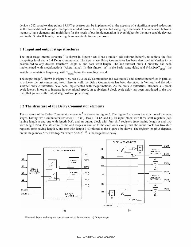
3.1 Input and output stage structures The input stage internal structure 8 is shown in Figure 4.a); it has a radix 4 add-subtract butterfly to achieve the first computing level and a 2:4 Delay Commutator. The input stage Delay Commutator has been described in Verilog to be customized to any desired transform length N and data word-length. The add-subtract radix 4 butterfly has been implemented with megafunctions (Altera name). In that figure, “∆” is the basic stage delay and f=1/(2•∆•Tclock) the switch commutation frequency, with Tclock being the sampling period.
The output stage 8, shown in Figure 4.b), has a 2:2 Delay Commutator and two radix 2 add-subtract butterflies in parallel to achieve the last computing level. Here as well, the Delay Commutator has been described in Verilog, and the add-subtract radix 2 butterflies have been implemented with megafunctions. As the radix 2 butterflies introduce a 3 clock cycle latency in order to increase its operational speed, an equivalent 3 clock cycle delay has been introduced to the two lines that go across the output stage without processing.
3.2 The structure of the Delay Commutator elements
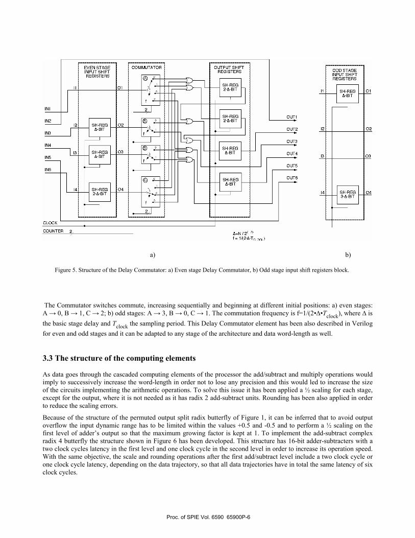
The structure of the Delay Commutator elements 8 is shown in Figure 5. The Figure 5.a) shows the structure of the even stages, having two Commutator switches 1 : 2 (B), two 1 : 4 (A and C), an input block with three shift registers (two having length ∆ and one with length 2•∆), and an output block with four shift registers (two having length ∆ and two with length 2•∆). The structure of the odd stages is similar to the even ones except that the input block has two shift registers (one having length ∆ and one with length 3•∆) placed as the Figure 5.b) shows. The register length ∆ depends on the stage índex “i” (0<i< log2N), where ∆=N/2(i+2) is the stage basic delay.
a) b)
Figure 4. Input and output stage structures: a) Input stage, b) Output stage
Proc. of SPIE Vol. 6590 65900P-5
A=N /20f = l/(2AT0)
ODD STAGEINPUT SHIFTREGISTERSOl
2 02
13 03
14 SH-REG3 A-BIT
04
a) b)
Figure 5. Structure of the Delay Commutator: a) Even stage Delay Commutator, b) Odd stage input shift registers block.
The Commutator switches commute, increasing sequentially and beginning at different initial positions: a) even stages: A → 0, B → 1, C → 2; b) odd stages: A → 3, B → 0, C → 1. The commutation frequency is f=1/(2•∆•Tclock), where ∆ is the basic stage delay and Tclock the sampling period. This Delay Commutator element has been also described in Verilog for even and odd stages and it can be adapted to any stage of the architecture and data word-length as well.
3.3 The structure of the computing elements As data goes through the cascaded computing elements of the processor the add/subtract and multiply operations would imply to successively increase the word-length in order not to lose any precision and this would led to increase the size of the circuits implementing the arithmetic operations. To solve this issue it has been applied a ½ scaling for each stage, except for the output, where it is not needed as it has radix 2 add-subtract units. Rounding has been also applied in order to reduce the scaling errors.
Because of the structure of the permuted output split radix butterfly of Figure 1, it can be inferred that to avoid output overflow the input dynamic range has to be limited within the values +0.5 and -0.5 and to perform a ½ scaling on the first level of adder’s output so that the maximum growing factor is kept at 1. To implement the add-subtract complex radix 4 butterfly the structure shown in Figure 6 has been developed. This structure has 16-bit adder-subtracters with a two clock cycles latency in the first level and one clock cycle in the second level in order to increase its operation speed. With the same objective, the scale and rounding operations after the first add/subtract level include a two clock cycle or one clock cycle latency, depending on the data trajectory, so that all data trajectories have in total the same latency of six clock cycles.
Proc. of SPIE Vol. 6590 65900P-6
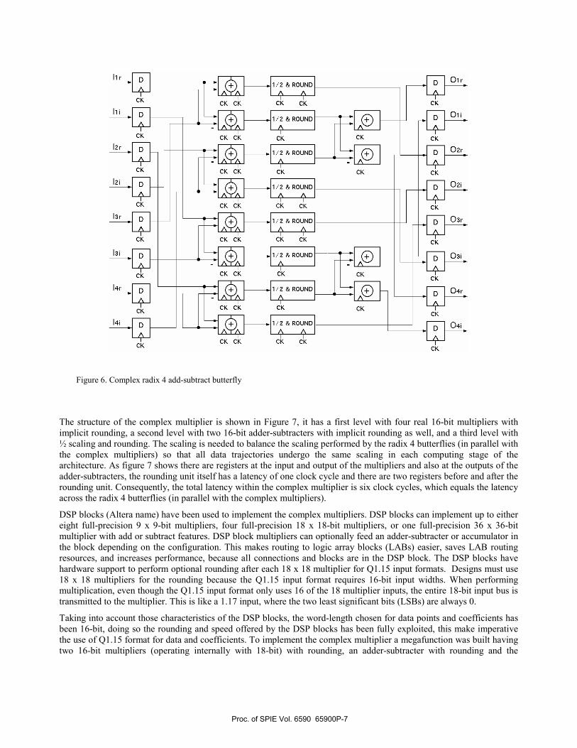
CK CK
Figure 6. Complex radix 4 add-subtract butterfly
The structure of the complex multiplier is shown in Figure 7, it has a first level with four real 16-bit multipliers with implicit rounding, a second level with two 16-bit adder-subtracters with implicit rounding as well, and a third level with ½ scaling and rounding. The scaling is needed to balance the scaling performed by the radix 4 butterflies (in parallel with the complex multipliers) so that all data trajectories undergo the same scaling in each computing stage of the architecture. As figure 7 shows there are registers at the input and output of the multipliers and also at the outputs of the adder-subtracters, the rounding unit itself has a latency of one clock cycle and there are two registers before and after the rounding unit. Consequently, the total latency within the complex multiplier is six clock cycles, which equals the latency across the radix 4 butterflies (in parallel with the complex multipliers).
DSP blocks (Altera name) have been used to implement the complex multipliers. DSP blocks can implement up to either eight full-precision 9 x 9-bit multipliers, four full-precision 18 x 18-bit multipliers, or one full-precision 36 x 36-bit multiplier with add or subtract features. DSP block multipliers can optionally feed an adder-subtracter or accumulator in the block depending on the configuration. This makes routing to logic array blocks (LABs) easier, saves LAB routing resources, and increases performance, because all connections and blocks are in the DSP block. The DSP blocks have hardware support to perform optional rounding after each 18 x 18 multiplier for Q1.15 input formats. Designs must use 18 x 18 multipliers for the rounding because the Q1.15 input format requires 16-bit input widths. When performing multiplication, even though the Q1.15 input format only uses 16 of the 18 multiplier inputs, the entire 18-bit input bus is transmitted to the multiplier. This is like a 1.17 input, where the two least significant bits (LSBs) are always 0.
Taking into account those characteristics of the DSP blocks, the word-length chosen for data points and coefficients has been 16-bit, doing so the rounding and speed offered by the DSP blocks has been fully exploited, this make imperative the use of Q1.15 format for data and coefficients. To implement the complex multiplier a megafunction was built having two 16-bit multipliers (operating internally with 18-bit) with rounding, an adder-subtracter with rounding and the
Proc. of SPIE Vol. 6590 65900P-7
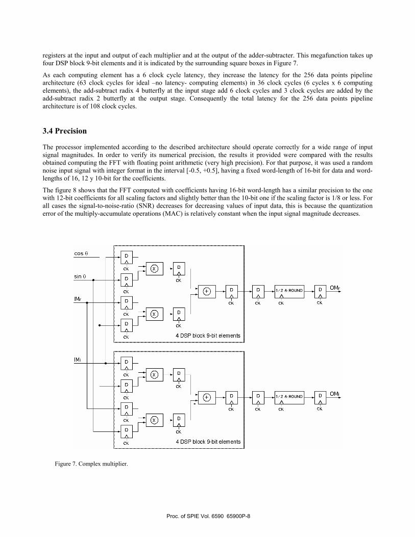
cos e
CK CK CK
registers at the input and output of each multiplier and at the output of the adder-subtracter. This megafunction takes up four DSP block 9-bit elements and it is indicated by the surrounding square boxes in Figure 7.
As each computing element has a 6 clock cycle latency, they increase the latency for the 256 data points pipeline architecture (63 clock cycles for ideal –no latency- computing elements) in 36 clock cycles (6 cycles x 6 computing elements), the add-subtract radix 4 butterfly at the input stage add 6 clock cycles and 3 clock cycles are added by the add-subtract radix 2 butterfly at the output stage. Consequently the total latency for the 256 data points pipeline architecture is of 108 clock cycles.
3.4 Precision The processor implemented according to the described architecture should operate correctly for a wide range of input signal magnitudes. In order to verify its numerical precision, the results it provided were compared with the results obtained computing the FFT with floating point arithmetic (very high precision). For that purpose, it was used a random noise input signal with integer format in the interval [-0.5, +0.5], having a fixed word-length of 16-bit for data and word-lengths of 16, 12 y 10-bit for the coefficients.
The figure 8 shows that the FFT computed with coefficients having 16-bit word-length has a similar precision to the one with 12-bit coefficients for all scaling factors and slightly better than the 10-bit one if the scaling factor is 1/8 or less. For all cases the signal-to-noise-ratio (SNR) decreases for decreasing values of input data, this is because the quantization error of the multiply-accumulate operations (MAC) is relatively constant when the input signal magnitude decreases.
Figure 7. Complex multiplier.
Proc. of SPIE Vol. 6590 65900P-8

ID
(1/1) (1/4) (I/B) (1/18) (1/32) (1/84)
70
80
so
40
3°
Coeff. (12-hit)
20
0
Scaling Factor for Random Noise Input Siwial
As precision is quite similar for coefficients having word-lengths of 16-bit or 12-bit, we could have used multipliers of 16 x 12-bit; but this would have render useless the built-in rounding unit in multipliers and adder-subtracters of the DSP blocks, as it only works when using for data and coefficients the Q1.15 format. Additionally it has been simulated the operation of the SRFFT architecture for 1024 data points from a random noise signal having fixed 16-bit word-length for both data and coefficients and obtaining a SNR 6dB lower than the SNR obtained for 256 data points (see figure 8). With word-lengths shorter than 16-bit the SNR for 1024 data points FFT would not yield acceptable results. From the results obtained with simulations the conclusion drawn is that the minimum requirements for the FPGA implementation of the 256 data points SRFFT are: 16-bit for the data-path and 16-bit for the coefficients word-length.
3.5 Simulation and comparison
For the processor implementation the compiler has allocated the following resources: 5 / 780 (4%) RAM blocks of 4K-bit, to implement the Delay Commutators shift registers and the coefficient ROM (the RAM block can emulate a ROM function using a dual-port RAM block); 6702 / 12480 (53%) ALUTs , to implement the add-subtract butterflies, the registers associated to the butterflies and some other registers used in the processor (6498); 96 / 96 (100%) DSP block 9-bit elements to implement the 48 16 x 16-bit multipliers of processor. As there are four complex input data channels (16-bit real and 16-bit imag), six complex output data channels (transform coefficients) and two single line inputs (reset & clk); the number of pins used for the processor are: (4x32)+(6x32)+2=322 pins from a total of 367 (87 % ). The results of the timing analysis using the simulator Quartus II Version 5.0 Web Edition, indicate a maximum operating frequency of 350 MHz, this provides a processing power of a 256 complex data points transform in 123 ns.
Table 1 shows some of the characteristics and the results of the simulation of our SRFFT processor and those of some other fixed point FFT processor previously reported: a single dual-port memory radix 4 processor 20, a dual memory radix 2/4 processor with serial input/output 21, and a pipeline radix 2 processor with serial input/output 22. The SRFFT processor presented here exhibits the highest processing power of all the FFT implemented with FPGA of Table 1.
Figure 8. SNR vs. Scaling Factor for a 256-point FFT.
Proc. of SPIE Vol. 6590 65900P-9

Processor [20] Altera FFT Core [21] Xilinx FFT Core [22] Our Design-AlteraNumber of points 1024 256 256 256 Datapath width (bit) 16 16 16 16
Combinational ALUTs ------ 2144 2027 6702 Logic registers ------ 3758 ------ 6498 18 x 18 multipliers ------ 12 30 48 Memory ------ 19 (9 K) 3 (36 K) 5 (4 K) Execution time(µs) 10.1 0.69 0.59 0.123 Frequency (MHz) 127 370 432 350 FPGA family Virtex II Pro 30 Stratix III Virtex 5 Stratix II Device XCV2P30 EP3SL70F484C2 5VSX35T EP2S15F672C3
Table 1. Performance comparison with other fixed-point FFT processors.
4. CONCLUSIONS This paper describes the design and FPGA implementation of a 256 complex data points pipeline SRFFT processor. The processor inputs are four parallel data channels (16-bit real & 16-imag, fixed-point within the range: –0.5, +0.5), and with a latency of 108 clock cycles, transform coefficients are output over six parallel data channels. The computing elements have an add-subtract butterfly operating in parallel with two multipliers, which have been implemented with the multipliers available within the FPGA in order to attain the highest possible operational speed; while the add-subtract butterflies have been implemented with the slower logic elements (LABs), but through segmentation (latency of 6 clock cycles) they have been adapted to operate at the same rate as the multipliers. The simulation of the processor predicts a capacity of performing a 256 data points SRFFT transform in 123 ns. for a (moderate) clock rate of 350 MHz.
ACKNOWLEDMENTS
This research has been supported by funds of the Spanish Ministry of Science and Technology (TIC2006-12438).
REFERENCES
1. T.-Y. Sung, “Memory-efficient and high-speed split-radix FFT/IFFT processor based on pipelined CORDIC rotations,” IEE Proc.-Vis. Image Signal Process., vol. 153, no. 4, pp. 405-410, Aug. 2006.
2. S. Magar, S. Shen, G. Luikuo, M. Fleming, and R. Aguilar, “An application specific DSP chip set for 100 MHz data rates,” in Proc. Int. Conf. Acoustics, Speech, and Signal Processing, vol. 4, pp. 1989-1992, Apr. 1988.
3. B.M. Baas, “A low-power, high-performance, 1024-point FFT processor,” IEEE J. Solid-State Circuits, vol. 34, pp. 380-387, Mar. 1999.
4. J. O’Brien, J. Mather, and B. Holland, “A 200 MIPS single-chip 1 k FFT processor ,” IEEE Int. Solid-State Circuits Conf. Dig. Tech. Papers, vol. 36, pp. 166-167, 1989.
5. L. R. Rabiner and B. Gold, Theory and Application of Digital Signal Processing, Prentice Hall Inc., ch. 10, 1975. 6. E.E. Swartzlander, W.K.W. Young, S.J. Joseph (1984), “A radix-4 Delay Commutator for fast Fourier transform
processor implementation,” IEEE J. Solid-State Circuits, vol. SC-19, pp. 702-709, Oct. 1984. 7. E.E. Swartzlander, V. K. Jain and H. Hikawa, “A radix-8 wafer scale FFT processor,” J. VLSI Signal Processing, 4,
pp. 165-176, May 1992. 8. J. García, J. A. Michell, and A. M. Burón, “VLSI configurable Delay Commutator for a pipeline split radix FFT
architecture,” IEEE Trans. Signal Processing, vol. 47, pp. 3098-3107, Nov. 1999. 9. Y.-W. Lin, H.-Y. Liu and C.-Y. Lee, “A 1-GS/s FFT/IFFT processor for UWB applications,” IEEE J. Solid-State
Circuits, vol. 40, no. 8, pp. 1726-1735, Aug. 2005.
Proc. of SPIE Vol. 6590 65900P-10

10. E. H. Wold and A. M. Despain, “Pipeline and parallel-pipeline FFT processors for VLSI implementations,” IEEE Trans. on Computers, vol. C-33, pp. 414-426, May 1984.
11. A. M. Despain, “Fourier transform computer using CORDIC iterations,” IEEE Trans. on Computers, vol. C-23, pp. 993-1001, Oct. 1974.
12. G. Bi and E. V. Jones, “A pipelined FFT processor for word-sequential data,” IEEE Trans. on Acoust., Speech, and Signal Processing, vol. 37, pp. 1982-1985, Dec. 1989.
13. E. Bidet, D. Castelain, C. Joanblank, and P. Stenn, “A fast single-chip implementation of 8192 complex point FFT,” IEEE J. Solid-State Circuits, vol. 30, pp. 300-305, Mar. 1995.
14. S. He and M. Torkelson, “Design and Implementation of a 1024-point pipeline FFT processor,” IEEE Custom Integrated Circuits Conference, pp. 131-134, 1998.
15. J.-Y. Oh and M.-S. Lim, “New radix-2 to the 4th power pipeline FFT processor,” IEICE Trans. Electron., vol. E88-C, no. 8, pp. 1740-1746, Aug. 2005.
16. W.-C. Yeh and C.-W. Jen, “High-speed and low-power split-radix FFT,” IEEE Trans. on Acoust., Speech, and Signal Processing, vol. 51, no. 3, pp. 864-874, Mar. 2003.
17. P. Duhamel and H. Hollmann, “Split-Radix FFT Algorithm.” Electron. Lett., vol. 20, no. 1, pp. 14-16, Jan. 1984. 18. P. Duhamel, “Implementation of ‘Split-Radix’ FFT Algorithms for Complex, Real, and Real-Symmetric Data,”
IEEE Trans. Acoust., Speech, and Signal Processing, vol. ASSP-34, no. 2, pp. 285-295, April 1986. 19. K. Zong, H. He and G. Zhu, “An ultra high-speed FFT processor,” IEEE Proc. Int. Sym. on Signals, Circuits and
Systems, pp. 37-40, 2003. 20. C. Chao, Z. Qin, X. Yingke and H. Chengde, “Design of a High performance FFT processor based on FPGA,” IEEE
Proc. Asia South-Pacific Design Automation Conf., pp. 920-923, Jan, 2005. 21. Datasheet, “FFT MegaCore function user guide,” Version 7.0, Altera Inc., Dec. 2006. 22. Datasheet, “Xilinx LogiCore Fast Fourier Transform,” Version 4.1, Xilinx Inc., Feb. 2007.
Proc. of SPIE Vol. 6590 65900P-11
Related Documents


![Radix-2 FFT Bit Reversal Architecture to Process double Data …ijirt.org/master/publishedpaper/IJIRT146388_PAPER.pdf · 2018-05-14 · (SDF) [1], [2], single-path delay commutator](https://static.cupdf.com/doc/110x72/5e7fa8db5cf170546d27ac3a/radix-2-fft-bit-reversal-architecture-to-process-double-data-ijirtorgmasterpublishedpaperijirt146388paperpdf.jpg)