Low-Energy Radix-2 Serial and Parallel FFT Designs by DongNi Zhang B.A.Sc. in Electrical Engineering University of Waterloo, 2010 Submitted to the Department of Electrical Engineering and Computer Science in partial fulfillment of the requirements for the degree of Master of Science in Electrical Engineering and Computer Science at the MASSACHUSETTS INSTITUTE OF TECHNOLOGY September 2013 © Massachusetts Institute of Technology 2013. All rights reserved. Author.. ARc!4~ - Department of Electrical Engineering and Computer Science August 30, 2013 C ertified b y ................................ ..... ...... ............ Anantha P. Chandrakasan Joseph F. and Nancy P. Keithley Professor of Electrical Engineering Thesis Supervisor Accepted by............ LeslAlKolodziejski Chairman, Department Committee on Graduate Students

Welcome message from author
This document is posted to help you gain knowledge. Please leave a comment to let me know what you think about it! Share it to your friends and learn new things together.
Transcript
Low-Energy Radix-2 Serial and Parallel FFT Designs
by
DongNi Zhang
B.A.Sc. in Electrical EngineeringUniversity of Waterloo, 2010
Submitted to the Department of Electrical Engineering and Computer Sciencein partial fulfillment of the requirements for the degree of
Master of Science in Electrical Engineering and Computer Science
at the
MASSACHUSETTS INSTITUTE OF TECHNOLOGY
September 2013
© Massachusetts Institute of Technology 2013. All rights reserved.
Author..
ARc!4~ -
Department of Electrical Engineering and Computer ScienceAugust 30, 2013
C ertified b y ................................ ..... ...... ............Anantha P. Chandrakasan
Joseph F. and Nancy P. Keithley Professor of Electrical EngineeringThesis Supervisor
Accepted by............LeslAlKolodziejski
Chairman, Department Committee on Graduate Students

Low-Energy Radix-2 Serial and Parallel FFT Designs
by
DongNi Zhang
Submitted to the Department of Electrical Engineering and Computer Scienceon August 30, 2013, in partial fulfillment of the
requirements for the degree of
Master of Science in Electrical Engineering and Computer Science
Abstract
The push for portable electronics for communication and biomedical applicationshas accelerated the growing momentum for high performance and low energyhardware implementations of the Fast Fourier Transform (FFT). This workpresents several new hardware implementations of the radix-2 FFT algorithmsthat take advantage of intermittent data and parallelism to reduce the energyper FFT.
In the modified serial design, by using a low-power control memory and apipelined data look-ahead controller to optimize processing of sequences of datawith zeros, up to 45% of energy savings are achieved as compared to the baselinedesign. Two fully parallel FFTs with different datapaths are also developedbased on a FFT flow diagram with the same geometry in each stage. Energysavings of up to 90% (an order of magnitude) are achieved as compared to thebaseline design. These results are demonstrated through post-layout andparasitic extraction Nanosim simulations with 90nm standard cell libraries.
Thesis Supervisor: Anantha P. Chandrakasan
Title: Joseph F. and Nancy P. Keithley Professor of Electrical Engineering


Acknowledgements
My journey at MIT throughout the past three years has truly been one of a
kind. With family, health, and all the aspects of life packaged onto one roller
coaster ride, I am truly thankful for the people in my life that made my years at
MIT deeply memorable.
First and foremost, I want to thank my research advisor, Professor Anantha
Chandrakasan, for taking me into his group, for being so sensitive and
understanding of my situation and needs, for providing me with invaluable
research advice and guidance, and for having faith and confidence in me
throughout the past year. Throughout a few research glitches where I panicked,
he never failed to assure me with "please don't worry". And while I now realize
that his technical intuitions are always right, he was always humble and
encouraged me to seek what I thought was right, even if I knew it conflicted
with his predictions. I am very honored and grateful to have had Prof.
Chandrakasan as my advisor. Without his motivation, inspiration, kindness,
and patience, this thesis would not have been possible.
I also remain forever indebted to a few other professors, Professor Joel
Dawson, Professor David Perrault, and Professor David Nairn (from the
University of Waterloo). They not only taught me invaluable RF/power
5

electronics/analog circuit fundamentals, but have also become friends that I can
confide in over the years.
Next, I want to express my sincere gratitude towards my colleague Rui Jin,
for his immense research contributions to the modified serial FFT architecture
proposed in this thesis. His understandings of the existing design, research and
analysis of the improved design, as well as proficiencies and resourcefulness
with tools, especially Cadence Encounter tools, have made the implementations
of multiple power domain designs possible for this research.
Additionally, I want to give my sincere appreciations to Nathan Ickes, Joyce
Kwong, Yildiz Sinangil, and Gilad Yahalom for taking the time out of their busy
schedule to allow me to consult with them on the various aspects of the designs.
I am also grateful to Margaret Flaherty and the rest of the research group for
sources of inspiration and the never-dull moments in the lab.
I have been fortunate to have met many friends here at MIT whom
encouraged me along the way and made my everyday worthwhile. Pleading
paucity of space, I want to give a few special shout-outs. Bonnie Lam, thank
you for all of our fun times together shopping, going to free food events, and
hanging out in each other's dorms. Bernhard Zimmermann, remember all the
late nights finishing problem sets together over bowls of fruits, smoothies, and
the lamp? I am glad we balanced it out with going sailing and exploring Boston
together. Maria de Soria, I had so much fun hanging out with you, cooking fish
6

together over Champaign, and talking about boys. Debb Hodges-Pabon, I will
forever remember all our sacred tree walks together. Gilad Yahalom, Sushmit
Goswami, Muyiwa Ogunnika, Mandy Woo, Kendall Nowocin, Georgia Lagoudas,
and Annie Chen, you guys are the best! I cherish all of you very much, and I
look forward to our life-long friendships.
Last but certainly not least, I want to thank my most loving parents,
Jinying Guo and Zheng Zhang, and the love of my life, Adam Bray, for giving
me endless love, support and encouragement for as long as I can remember. I
know that I can always lean on you when I am beaten to the ground. You are
the source of my strength and happiness in life, and I owe my life to you.
7

8

Table of Contents
Abstract ................................................................................................................ 3
Acknowledgm ents ............................................................................................... 5
Table of Contents .................................................................................................. 9
List of Figures ..................................................................................................... 13
List of Tables ...................................................................................................... 15
1. Introduction ................................................................................................... 17
1. 1 M otivation .............................................................................................. 17
1.2 Thesis Outline ........................................................................................ 18
1.3 Contributions ......................................................................................... 19
2. Background ...... o ............................................. o ....................... o ....................... 21
2.1 FFT Algorithm s ..................................................................................... 21
2.2 Figures of M erit ..................................................................................... 24
2.3 Previous W ork ........................................................................................ 26
3. Baseline Serial Radix-2 FFT Architecture ..... o .............................................. 31
3.1 State M achine ........................................................................................ 32
3.2 M em ory Partitioning ............................................................... QA
3.3 Address Generation ............................................................................... 35
3.4 Datapath ................................................................................................ 36
9

4. Proposed Radix-2 FFT Architectures ............................................................ 37
4.1 M odified Serial Architecture ............................................................ 37
4.1.1 State M achine ....................................................................... 39
4.1.2 Control M em ory ................................................................... 40
4.1.3 Controller .............................................................................. 41
4.2 Parallel Architecture ......................................................................... 43
4.2.1 State M achine ....................................................................... 46
4.2.2 Im plicit M em ory ................................................................... 47
4.2.3 Datapath ................................................................................ 47
4.3 M odified Parallel Architecture .......................................................... 48
4.3.1 State M achine ....................................................................... 50
4.3.2 Implicit M em ory ................................................................... 51
4.3.3 Datapath ................................................................................ 51
5. Sim ulation Results ..................................................................................... 53
5.1 Tools and Sim ulation Flow ............................................................... 53
5.2 M odified Serial vs. Baseline ............................................................... 56
5.3 Parallel vs. M odified Parallel vs. Baseline ...................................... 63
6. Conclusions................................................................................................ 73
A. Alternative Form s of FFT Flow Diagram s .................................................... 77
B. Baseline Im plem entation Details ............................................................... 79
10

C. Booth M ultiplier Algorithm s ...................................................................... 81
Bibliography ................................................................................................... 83
11

12
List of Figures
Figure 2.1: Flow Graph of the Complete Decomposition of an 8-point DFT [2]..23
Figure 2.2: Flow Graph of a Single Butterfly [2].............................................23
Figure 2.3: Source of Active Energy in CMOS Inverter [3] ............................. 25
Figure 2.4: Minimum-Energy Operating Point [5]...........................................28
Figure 2.5: Dynamic Voltage and Frequency Scaling (DVFS) [6] ................... 29
Figure 3.1: Baseline Design Block-Diagram .................................................... 31
Figure 3.2: Baseline Design Finite State Machine (FSM) ............................... 32
Figure 3.3: Memory Access Timing Diagram ................................................... 33
Figure 3.4: 8-point FFT Butterfly Sequence......................................................35
Figure 4.1: Modified Serial FFT Block Diagram ............................................. 39
Figure 4.2: FFT Decimation in Time with Same Geometry in Each Stage [1] ...43
Figure 4.3: Parallel FFT Block-Diagram .......................................................... 45
Figure 4.4: Parallel Design FSM ....................................................................... 46
Figure 4.5: Modified Parallel FFT Block-Diagram (8-point FFT Shown) ..... 49
Figure 4.6: M odified Parallel Design FSM ....................................................... 50
Figure 5.1: Normalized (Point-by-Point) Modified Serial FFT Simulation Results
................................................................................................................................ 5 7
Figure 5.2: Normalized (Highest-Point) Modified Serial FFT Simulation Results
................................................................................................................................ 5 8
Figure 5.3: Energy Breakdown of Blocks in Serial FFT Systems (Ozero) ..... 60
13
Figure 5.4: Data Memory Energy..................................................................... 61
Figure 5.5: D atapath Energy............................................................................ 61
Figure 5.6: Overhead Energy ........................................................................... 62
Figure 5.7: ROM /Other Energy......................................................................... 62
Figure 5.8: Modified Serial FFT Layout and Floorplan....................................63
Figure 5.9: Normalized (Point-by-Point) Energy Simulation Results vs. % of
z e ro s ........................................................................................................................ 6 5
Figure 5.10: Normalized (Highest-Point) Energy Simulation Results vs. % of
z e ro s ........................................................................................................................ 6 7
Figure 5.11: Normalized (Point-by-Point) Energy Simulation Results vs.
P erform an ce ..................................................................................................... . . 68
Figure 5.12: Normalized (Highest-Point) Energy Simulation Results vs.
P erform an ce ..................................................................................................... . . 69
Figure 5.13: Parallel FFT Layout and Floorplan ............................................. 70
Figure 5.14: Modified Parallel FFT Layout and Floorplan..............................71
Figure A. 1: FFT Decimation-in-Time with Input in Normal Order [1]...........77
Figure A.2: FFT Decimation-in-Time with Input and Output in Normal Order
[ ].............................................................................................................................7 8
Figure A.3: FFT Decimation-in-Frequency with Input in Normal Order [1]......78
14
List of Tables
Table 2.1: Recent FFT Chips and Contributions.............................................30
Table 3.1: Memory Partitioning for an 8-point FFT.........................................34
Table 4.1: Four Variations of the Modified Serial Design Topologies ............. 42
Table 5.1: Tools, Simulation and Design Flow ................................................. 54
T able 5.2: T est C ases ........................................................................................ 55
Table 5.3: Test Cases and Param eters.............................................................. 64
Table B.1: Input Ordering vs. Address Locations of an 8-point FFT .............. 79
Table B.2: Address Generation for an 8-point FFT ......................................... 80
Table B.3: Address Generation for an 8-point FFT .......................................... 80
Table C. 1: Booth Algorithm LSB Combinations [11] ...................................... 81
Table C.2: Booth Algorithm Example 1........................................................... 82
15

16

Chapter 1
Introduction
1.1 Motivation
There is no shortage of signals to be sampled - audio, video, and
spectrum, to name a few. The ability to interpret the acquired data through
real-time computation of the Fast Fourier Transform (FFT) is the foundation for
monitoring, analyzing, and controlling various systems.
The FFT is an efficient algorithm that extracts the frequency contents
from a time-domain signal. It is one of the most fundamental, yet power-hungry
blocks in digital signal processing because it is computationally intensive. With
advancements in low-power designs, energy efficient FFT processors have
become an integral part of energy-constrained applications such as modern
telecommunication, sensor networks, and portable biomedical devices.
17

The purpose of this thesis is to present various architectural changes
which further reduce the energy consumption of the existing 32-point 16-bit
resolution serial radix-2 FFT engine (e.g. by Kwong in [1]), while maintaining
its performance. This investigation explores the impact of parallelism and data
dependency on the energy efficiency of FFT coupled with voltage scaling.
1.2 Thesis Outline
This thesis is divided into 6 main chapters. Chapter 1 introduces the
motivation behind this investigation, as well as the outline and main
contributions of the thesis. Chapter 2 presents relevant background concepts on
FFT algorithms, along with the figure of merits. Common low-power techniques
and an overview of the previous work on low-power FFT designs in the
literature are also introduced. Chapter 3 dives more in-depth into the designs
of the baseline serial architecture which all other designs will be based on or
compared against. Chapter 4 presents the computation algorithms and design
considerations for the three alternate radix-2 FFT architectures proposed.
Chapter 5 touches on the tools and simulation flow used to obtain the
simulation results. Additionally, a comprehensive energy comparison between
the architectures for different percentage of zero-data and performance
specifications are demonstrated through figures. And Finally, Chapter 6
concludes the thesis by summarizing the major findings within the thesis as
well as recommending future considerations and directions for this research.
18
1.3 Contributions
In this thesis, three main radix-2 FFT architectures are proposed. Post-
layout and parasitic extraction Nanosim simulations with 90nm standard cell
libraries are used to demonstrate energy saving comparisons.
The first is a modified serial design that utilizes techniques such as clock
gating, power gating, and voltage scaling in conjunction with data prediction to
reduce energy. Data with zeros are commonly found in signals. In applications
such as the sensor system, intermittent signals often contain clumps of zeros.
In many other signals, zeros are often scattered randomly throughout the
signal. In both cases, a pre-processing controller is developed to exploit data-
dependency to reduce memory access and computational datapath switching
activity. By using a low-power control memory and a pipelined data look-ahead
controller to optimize processing of sequences of data with zeros, up to 45% of
energy savings are achieved as compared to the baseline design.
The second and third are two new parallel designs that exploit
parallelism to reduce supply voltage. Two fully parallel FFTs with different
datapaths are developed based on a FFT flow diagram with the same geometry
in each stage. The fewer cycle count allow for clock frequency to be greatly
reduced, which in turn allow for a reduction in supply voltage. Energy savings
of up to 90% (an order of magnitude) are achieved as compared to the baseline
design.
19

20

Chapter 2
Background
2.1 FFT Algorithms
Before diving into the hardware implementation of the FFT cores, a brief
FFT background theory is given in this section. A continuous-time signal x[t]
can be sampled at intervals of T, to create a discrete time-domain sequence x[n].
x[n] = x[nT,], -oo < n < oo (2.1) [2]
x[n] can be uniquely mapped to a continuous and periodic frequency-domain
representation X(ej") called the Discrete-Time Fourier Transform (DTFT).
X(e" ) = x[n]e-j&)n
7 - oo
co periodic every 27 interval
21
(2.2) [2]
Sampling the DTFT of a finite N-length x[n] produces an N-point discrete and
periodic frequency-domain representation X[k] called the Discrete Fourier
Transform (DFT).
N-1
X[k] = x[n]Wk , WN = e~( , k = 0,1, ...,N - 1 (2.3) [2]n=O
Assuming the number of arithmetic multiplications and additions is a
measure of computational complexity, the Fast Fourier Transform (FFT) is an
efficient algorithm for computing the DFT [2]. As a comparison, for a
complex x[n], the direct evaluation of the DFT through Eq. (2.3) requires a total
ofN 2 complex multiplications and N(N - 1) complex additions. In contrast, a
radix-2 FFT algorithm requires only 1o 2N complex multiplications
and N1o 2N complex additions [2].
This is due to the fact that FFT algorithms are based on recursively
decomposing the DFT of an N-length sequence into smaller-length DFT that are
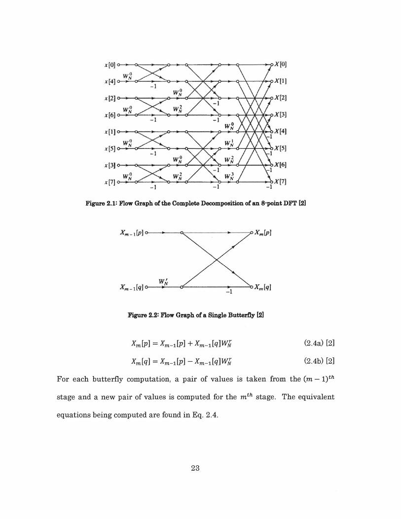
then combined together. Figure 2.1 shows the flow graph of the complete
decomposition for an 8-point DFT. Appendix A lists a few alternative forms of
the FFT flow diagram. A fully decomposed DFT is referred to as a radix-2 FFT,
as the computation is reduced to that of 2-point DFT. The 2-point DFT block is
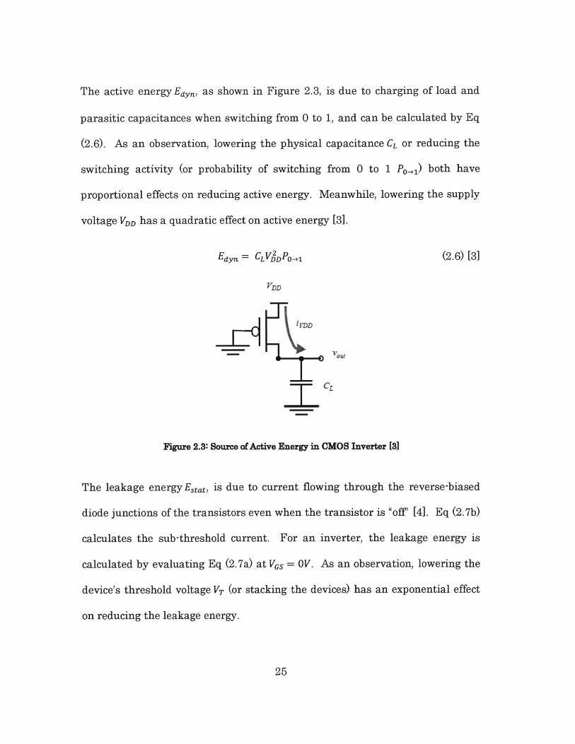
referred to as a butterfly and is shown in Figure 2.2. In a radix-2 N-point FFT,
there are Nlo 2N stages, with each stage containing L basic blocks.
22
x[(0]
44]x[4] P X[1]
x [2) -+- X[2]
x[6]o- >- 3j X[31
x{1]WIO X[4)
x [7J - -- 5
WNW WN
x [31 $-N-cWN X16]
x[7] 0 o X [71
Figure 2.1: Flow Graph of the Complete Decomposition of an 8-point DFT [21
X.-1 [PJO....--D XM[PI
WN"Xm, [qJ 1P- Xm[qJ
Figure 2.2: Flow Graph of a Single Butterfy [21
Xm[p] = Xm-[p] + Xm-1[q]W4 (2.4a) [2]
Xm[q] = Xm_1[p] - Xm. 1[q]W4 (2.4b) [2]
For each butterfly computation, a pair of values is taken from the (m - 1)th
stage and a new pair of values is computed for the mth stage. The equivalent
equations being computed are found in Eq. 2.4.
23

2.2 Figures of Merit
To quantitatively evaluate and compare various hardware
implementations of the FFT algorithm, a set of figures of merit are introduced
here.
The first metric is performance. In this investigation, the
performance tone FFT is defined as the total time taken to finish computing one
FFT. So for a given performance specification, the minimum clock
frequency fclk,min can be calculated by Eq. (2.5) if the number of cycles needed to
perform the calculation, ncycles taken, is fixed for an architecture.
tone FFT I fclkmn - ncycles taken (2.5)-cycles taken tone FFT
For a given process, there is a maximum supply voltage VDD which the design
can operate at, which sets a lower bound for the propagation delay. Depending
on the design architecture, if the critical path is too long, there may not exists a
clock frequency that satisfies both Eq. (2.5) and the setup and hold time
constraints, in which case the design simply cannot meet performance. With
performance requirement as a variable, this investigation compares various
designs for different performance specifications.
The second metric is energy consumption per FFT, with main focus on
the dynamic (or switching) energy and the static (leakage) energy in this work.
24
The active energy Edyn, as shown in Figure 2.3, is due to charging of load and
parasitic capacitances when switching from 0 to 1, and can be calculated by Eq
(2.6). As an observation, lowering the physical capacitance CL or reducing the
switching activity (or probability of switching from 0 to 1 P0 , 1) both have
proportional effects on reducing active energy. Meanwhile, lowering the supply
voltage VDD has a quadratic effect on active energy [3].
Edyn = CLVjDPo l (2.6) [3]
VDD
iVDD
"out
Figure 2.3: Source of Active Energy in CMOS Inverter [3]
The leakage energy Estat, is due to current flowing through the reverse-biased
diode junctions of the transistors even when the transistor is "off' [4]. Eq (2.7b)
calculates the sub-threshold current. For an inverter, the leakage energy is
calculated by evaluating Eq (2.7a) at VGS = OV. As an observation, lowering the
device's threshold voltage VT (or stacking the devices) has an exponential effect
on reducing the leakage energy.
25

Estat =VDD toneFFT isub(t) dt (2.7a) [4]ft=0
VGS-VT+rVDS VDS) (2.7b) [4]Isub = 0 e nth 1 - e Vth
Other metrics of less importance for the purpose of this investigation
include the cost or area of the chip, the resolution (which is fixed at 16-bit), and
the number of points N (which is fixed at 32-point) for the designs discussed in
this thesis.
In general for any hardware design, a tradeoff exists between
performance and energy. In the context of this quest, the goal is to achieve
lower energy per FFT for a given performance specification. This is different
from the goal of minimizing energy regardless of performance.
2.3 Previous Work
This section will give a brief overview on the common low-power design
techniques and the achievements of other scholars in the field of low-energy
FFT processor design. Clock gating, power gating and voltage scaling are some
of the common techniques used in low-power designs.
Clock gating is a technique that adds more logic to prune the clock tree.
By disabling portions of the circuit flip flops from switching state when disable
26

conditions are set, switching power consumption goes to zero, and only leakage
power are incurred [12].
Power gating is a technique that shuts off the supply current to blocks of
the circuit via switching transistors placed at header and/or footer. By stacking
transistors during system stand-by, the leakage power can be reduced [4].
However, entering and exiting the sleep mode safely also increases timing
delays. Moreover, architectural trade-off exists between leakage energy saved
in stand-by mode and the energy consumed to enter and exit the sleep mode [4].
Power gating methods such as the fine-grain power gating, coarse-grain power
gating are sometimes used, and will not be covered in details here. Other cells
of importance often used in power gating circuitry include the isolation cells and
retention registers. Isolation cells are usually placed in between the power
gated block and the normally-On block the first is driving. This prevents the
short circuit current in the normally-On block caused by its floating input when
the first block is put to sleep [13]. Retention blocks are usually composed of low
leakage flip flops used to hold the data when entering sleep and restore the
system state when the system is reawakened [13].
Dynamic voltage scaling is a technique that increases or decreases the
supply voltage to a block depending on the circumstances. Increasing the
supply voltage is sometimes used to increase the performance of a circuitry, as it
causes capacitances to be charged and discharged quicker [3]. Decreasing the
supply voltage is sometimes used to save power, as the switching power
27
dissipated by static CMOS gates decreases quadratically with decreasing
voltage (Eq. 2.6).
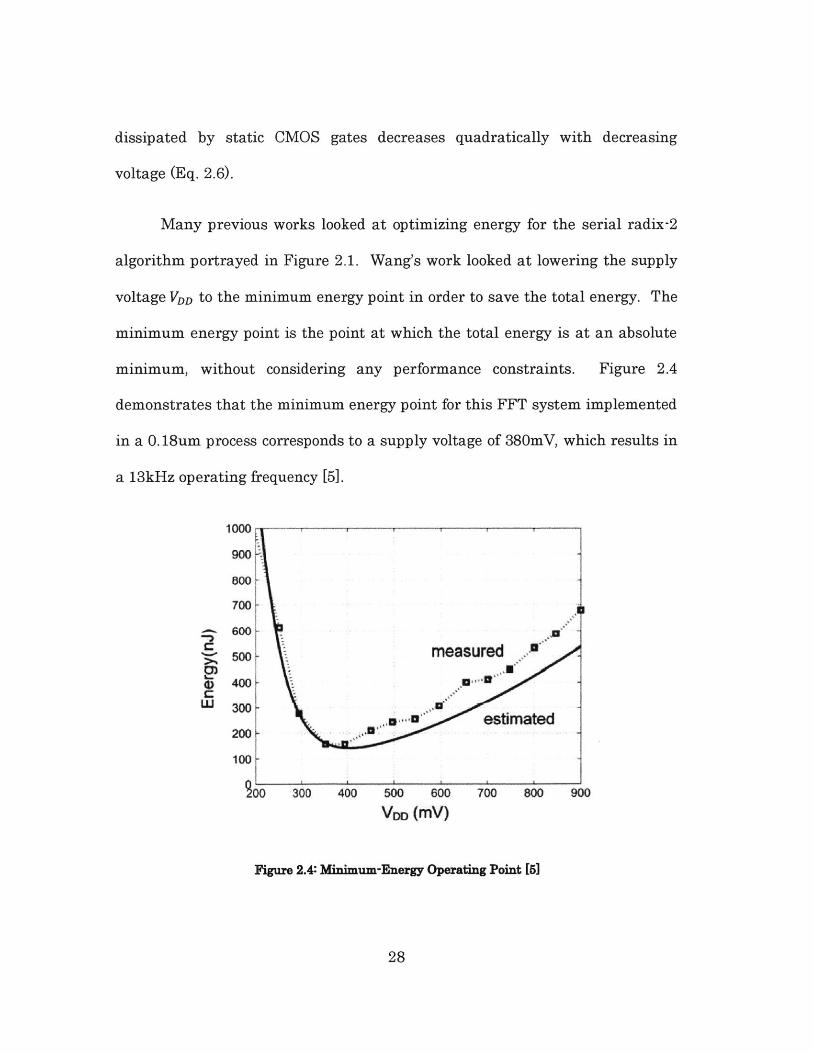
Many previous works looked at optimizing energy for the serial radix-2
algorithm portrayed in Figure 2.1. Wang's work looked at lowering the supply
voltage VDD to the minimum energy point in order to save the total energy. The
minimum energy point is the point at which the total energy is at an absolute
minimum, without considering any performance constraints. Figure 2.4
demonstrates that the minimum energy point for this FFT system implemented
in a 0. 18um process corresponds to a supply voltage of 380mV, which results in
a 13kHz operating frequency [5].
900
800
700
600 .
0)"5W0 measured.
4 400
W 300F Iestimated
200-
100
900 300 400 500 600 700 800 900
VDD (mV)
Figure 2.4: Minimum-Energy Operating Point [51
28
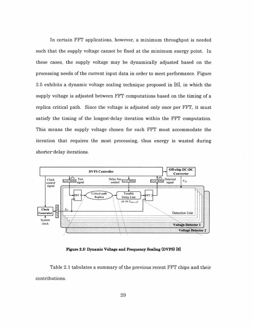
In certain FFT applications, however, a minimum throughput is needed
such that the supply voltage cannot be fixed at the minimum energy point. In
these cases, the supply voltage may be dynamically adjusted based on the
processing needs of the current input data in order to meet performance. Figure
2.5 exhibits a dynamic voltage scaling technique proposed in [6], in which the
supply voltage is adjusted between FFT computations based on the timing of a
replica critical path. Since the voltage is adjusted only once per FFT, it must
satisfy the timing of the longest-delay iteration within the FFT computation.
This means the supply voltage chosen for each FFT must accommodate the
iteration that requires the most processing, thus energy is wasted during
shorter-delay iterations.
DVFS Contro__er Off-chiip DC-DCConverter
Clock Test Delay line Detected
l~xcvc erUvol S I i " I Vo
control signal control signalsignal
FF I Critical-path Tunable sReplica
PCok flGenerator -!Detection Unit
SystemclockVot .lttr
Voltoge'Deectr 2
Figure 2.5: Dynamic Voltage and Frequency Scaling (DVFS) [6]
Table 2.1 tabulates a summary of the previous recent FFT chips and their
contributions.
29
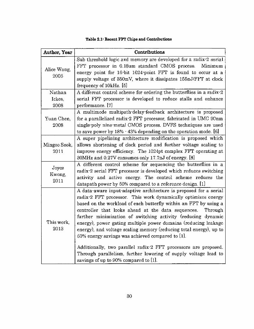
Table 2.1: Recent FFT Chips and Contributions
Author, Year Contributions
Sub threshold logic and memory are developed for a radix-2 serial
FFT processor in 0. 18um standard CMOS process. MinimumAieW ' energy point for 16-bit 1024-point FFT is found to occur at a
supply voltage of 350mV, where it dissipates 155nJ/FFT at clockfrequency of 10kHz. [5]
Nathan A different control scheme for ordering the butterflies in a radix-2Ickes, serial FFT processor is developed to reduce stalls and enhance2008 performance. [7]
A multimode multipath-delay-feedback architecture is proposedYuan Chen, for a parallelized radix-2 FFT processor, fabricated in UMC 90nm
2008 single-poly nine-metal CMOS process. DVFS techniques are usedto save power by 18% - 43% depending on the operation mode. [6]
A super pipelining architecture modification is proposed whichMingoo Seok, allows shortening of clock period and further voltage scaling to
2011 improve energy efficiency. The 1024pt complex FFT operating at30MHz and 0.27V consumes only 17.7nJ of energy. [8]A different control scheme for sequencing the butterflies in a
Joyce radix-2 serial FFT processor is developed which reduces switchingKwong activity and active energy. The control scheme reduces the
datapath power by 50% compared to a reference design. [1]A data-aware input-adaptive architecture is proposed for a serialradix-2 FFT processor. This work dynamically optimizes energybased on the workload of each butterfly within an FFT by using acontroller that looks ahead at the data sequences. Throughfurther minimization of switching activity (reducing dynamic
This work, energy), power gating multiple power domains (reducing leakage2013 energy), and voltage scaling memory (reducing total energy), up to
50% energy savings was achieved compared to [1].
Additionally, two parallel radix-2 FFT processors are proposed.Through parallelism, further lowering of supply voltage lead tosavings of up to 90% compared to [1].
30
Chapter 3
Baseline Serial Radix-2 FFT
Architecture
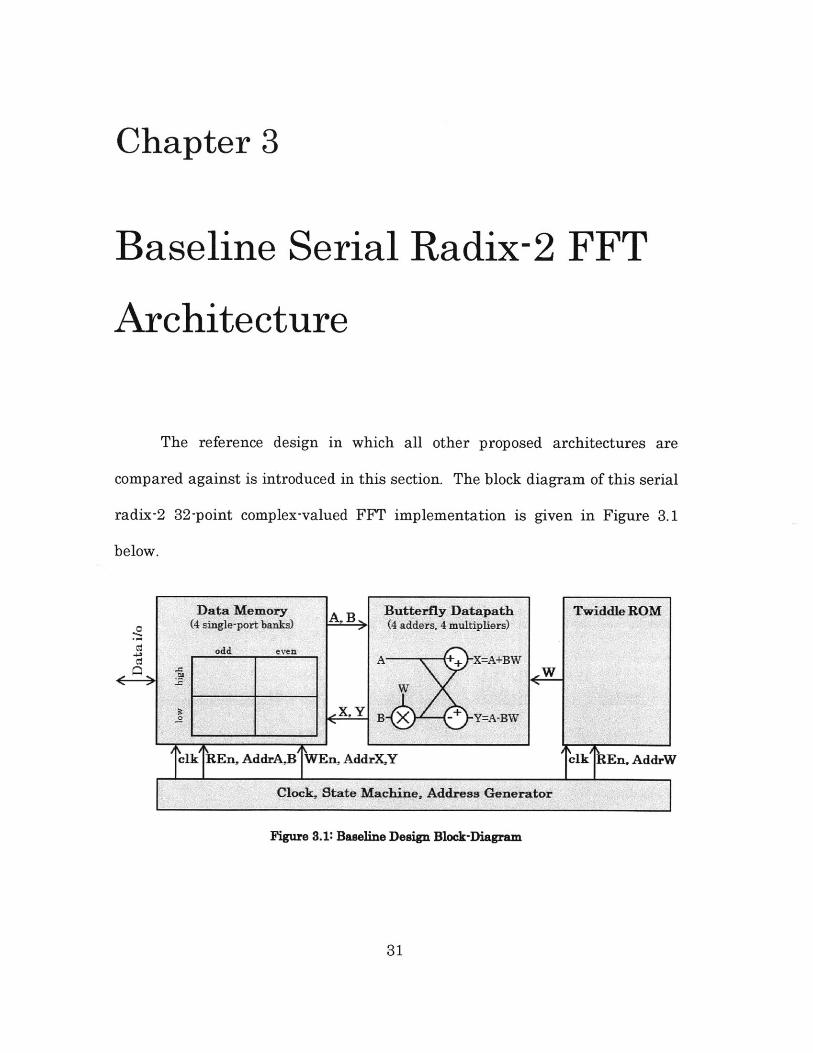
The reference design in which all other proposed architectures are
compared against is introduced in this section. The block diagram of this serial
radix-2 32-point complex-valued FFT implementation is given in Figure 3.1
below.
(4 single-port banks) A(B
odd even A
X~
t clkTRErk AddrA.BIWEn. AddrX.Y
W
Twiddle ROM
clk REn, AddrW
Clock, State Machine, Address Generator
Figure 3.1: Baseline Design Block-Diagram
31
0
flnt~m MjlmJIkw terfly Datapathadders, 4 multipliers)
+x=A+BW
wr
Bu

This design is directly based on Joyce Kwong's FFT implementation
found in [1], with truncation from 512-point down to 32-point to shorten power-
simulation time. In addition, flip-flop based memory is used in the simulation
instead of SRAM due to lack of access for this specific process.
3.1 State Machine
The 32-point serial implementation is based on the FFT algorithm in
32Figure 2.1, where there are -i-= 16 butterflies down in every stage and 109232 =
5 stages across, yielding a total of 80 butterflies. For this in-place computation,
the different nodes on the same horizontal line represent the same single
memory location that is updated through time.
The baseline system in Figure 3.1 operates in three stages: load, compute,
and unload, as illustrated by Figure 3.2 below.
reset) LOAD done load COMP done Comp) UNLD done unld DONE
Figure 3.2: Baseline Design Finite State Machine (FSM)
In the first stage, a time-domain input (real and imaginary) is written into the
data memory every clock cycle, until all 32 inputs are loaded.
32
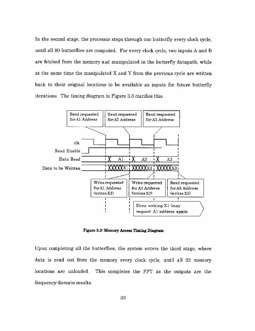
In the second stage, the processor steps through one butterfly every clock cycle,
until all 80 butterflies. are computed. For every clock cycle, two inputs A and B
are fetched from the memory and manipulated in the butterfly datapath, while
at the same time the manipulated X and Y from the previous cycle are written
back to their original locations to be available as inputs for future butterfly
iterations. The timing diagram in Figure 3.3 clarifies this.
Read
Dat
Data to be
Read requested Read requested Read requestedfor Al Address for A2 Address for A3 Address
clk
Enable
a Read X Al I A2 X A3
Written XX XlI XX X 2 XXX x3
Write requested Write requested Read requestedfor Al Address for A2 Address for A3 Address(writes X1) (writes X2) (writes X3)
I I
Done writing X1 (mayrequest Al address again
Figure 3.3: Memory Access Timing Diagram
Upon completing all the butterflies, the system enters the third stage, where
data is read out from the memory every clock cycle, until all 32 memory
locations are unloaded. This completes the FFT as the outputs are the
frequency-domain results.
33
3.2 Memory Partitioning
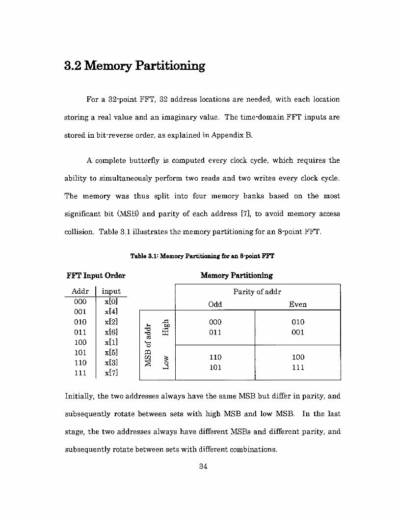
For a 32-point FFT, 32 address locations are needed, with each location
storing a real value and an imaginary value. The time-domain FFT inputs are
stored in bit-reverse order, as explained in Appendix B.
A complete butterfly is computed every clock cycle, which requires the
ability to simultaneously perform two reads and two writes every clock cycle.
The memory was thus split into four memory banks based on the most
significant bit (MSB) and parity of each address [7], to avoid memory access
collision. Table 3.1 illustrates the memory partitioning for an 8-point FFT.
FFT Input Order
Addr input000 x[0]001 x[4]010 x[2]011 x[6]100 x[1]101 x[5]110 x[3]111 x[7]
Table 3.1: Memory Partitioning for an 8-point FFT
Memory Partitioning
Parity of addr
Odd Even
1 000 010011 001
1 9: 110 100101 111
Initially, the two addresses always have the same MSB but differ in parity, and
subsequently rotate between sets with high MSB and low MSB. In the last
stage, the two addresses always have different MSBs and different parity, and
subsequently rotate between sets with different combinations.
34
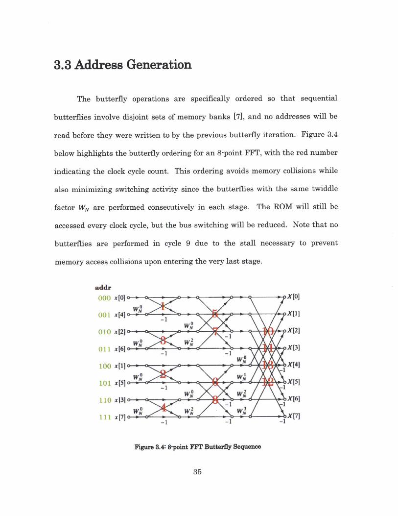
3.3 Address Generation
The butterfly operations are specifically ordered so that sequential
butterflies involve disjoint sets of memory banks [71, and no addresses will be
read before they were written to by the previous butterfly iteration. Figure 3.4
below highlights the butterfly ordering for an 8-point FFT, with the red number
indicating the clock cycle count. This ordering avoids memory collisions while
also minimizing switching activity since the butterflies with the same twiddle
factor WN are performed consecutively in each stage. The ROM will still be
accessed every clock cycle, but the bus switching will be reduced. Note that no
butterflies are performed in cycle 9 due to the stall necessary to prevent
memory access collisions upon entering the very last stage.
addr1.0 x[0] xX0
44-1 WoW
0 1 x[4] 0- o[J WN
x[6] WN X[31
-1 -1
3 pt(1 x[5 [5]
WoWN 3
1 1x[7] X[7]
FUpre 3.4: 8-point FFT Butterfly Sequence
35

This address sequence is generalized in Appendix B for all but the last stage. In
the last stage, the addresses are generated using gray-code counters instead.
The address generated for an 8-point FFT is shown in Appendix B.
3.4 Datapath
The datapath takes two pairs of complex numbers as inputs, implements
the butterfly in Figure 2.2 in hardware through combinational logics, and
outputs two pairs of complex numbers.
To implement Eq (3.2), the datapath requires 4 two-input multipliers to
calculate Br * Wr, Bi * Wi, Br * Wi, and Bi * Wr, along with 4 three-input adders to
calculate Xr, Xi, Y, and Y. This design uses the built-in Design Ware
multipliers and adders.
(Xr + jXi) = (Ar+ jA1 ) + (Br + jBi) * (Wr + jW)= (Ar+Br*Wr-Bi*Wi)+j(Ai+Br*Wi+Bi*Wr) (3.2a)
(Yr +Y) = (Ar +jA) - (Br +jBi) * (Wr +jWr)
= (Ar - Br * Wr + Bi * Wi) +j(Ai - Br * Wi - Bi * Wr) (3.2b)
36

Chapter 4
Proposed Radix-2 FFT
Architectures
Three architectures are proposed in this section, with the first one being
a direct modification of the reference design in [1], and the latter two being the
new parallel implementations. Functionally, all the designs produce the exact
same FFT results as the baseline design.
4.1 Modified Serial Architecture
This section looks at dynamically optimizing energy based on the
workload of each butterfly iterations within one FFT, as oppose to between
FFTs. The four variations of this proposed architecture are all based on the
reference design previously discussed. As noted in the Acknowledgement, the
37
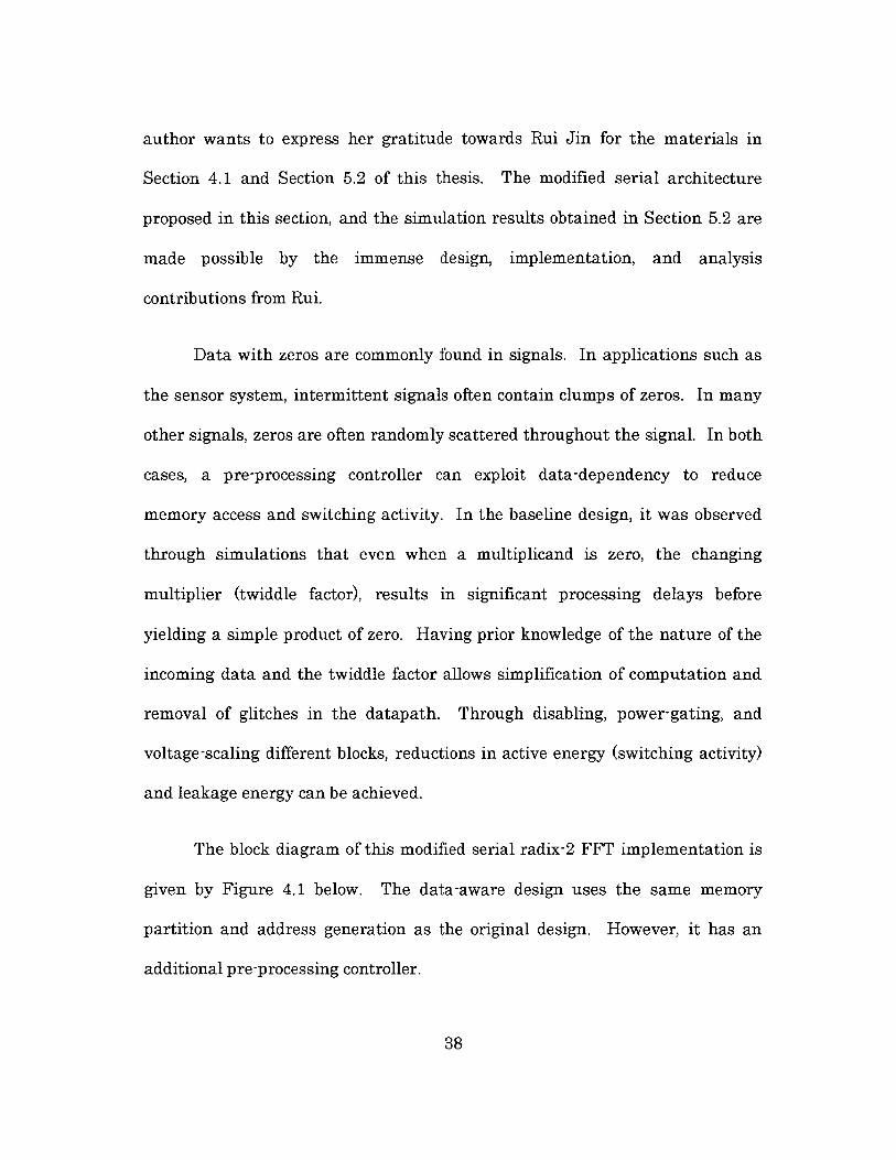
author wants to express her gratitude towards Rui Jin for the materials in
Section 4.1 and Section 5.2 of this thesis. The modified serial architecture
proposed in this section, and the simulation results obtained in Section 5.2 are
made possible by the immense design, implementation, and analysis
contributions from Rui.
Data with zeros are commonly found in signals. In applications such as
the sensor system, intermittent signals often contain clumps of zeros. In many
other signals, zeros are often randomly scattered throughout the signal. In both
cases, a pre-processing controller can exploit data-dependency to reduce
memory access and switching activity. In the baseline design, it was observed
through simulations that even when a multiplicand is zero, the changing
multiplier (twiddle factor), results in significant processing delays before
yielding a simple product of zero. Having prior knowledge of the nature of the
incoming data and the twiddle factor allows simplification of computation and
removal of glitches in the datapath. Through disabling, power-gating, and
voltage-scaling different blocks, reductions in active energy (switching activity)
and leakage energy can be achieved.
The block diagram of this modified serial radix-2 FFT implementation is
given by Figure 4.1 below. The data-aware design uses the same memory
partition and address generation as the original design. However, it has an
additional pre-processing controller.
38
VDDI
x 8 Power Gating
B X-
cl drAB AdrXYY'REn, WEn 'tnables
<w
Clock, State Machine, Address Generator
lkREn, AddrABWEn. AddrXY
TwiddleROM
elk, AddrW En
JREn. AddrW
Pre-Processing Controller
CD Control Memory XY flags L..gi.(4single-port banks)
odd even
Variable Pipeline
Figure 4.1: Modified Serial FFT Block Diagram
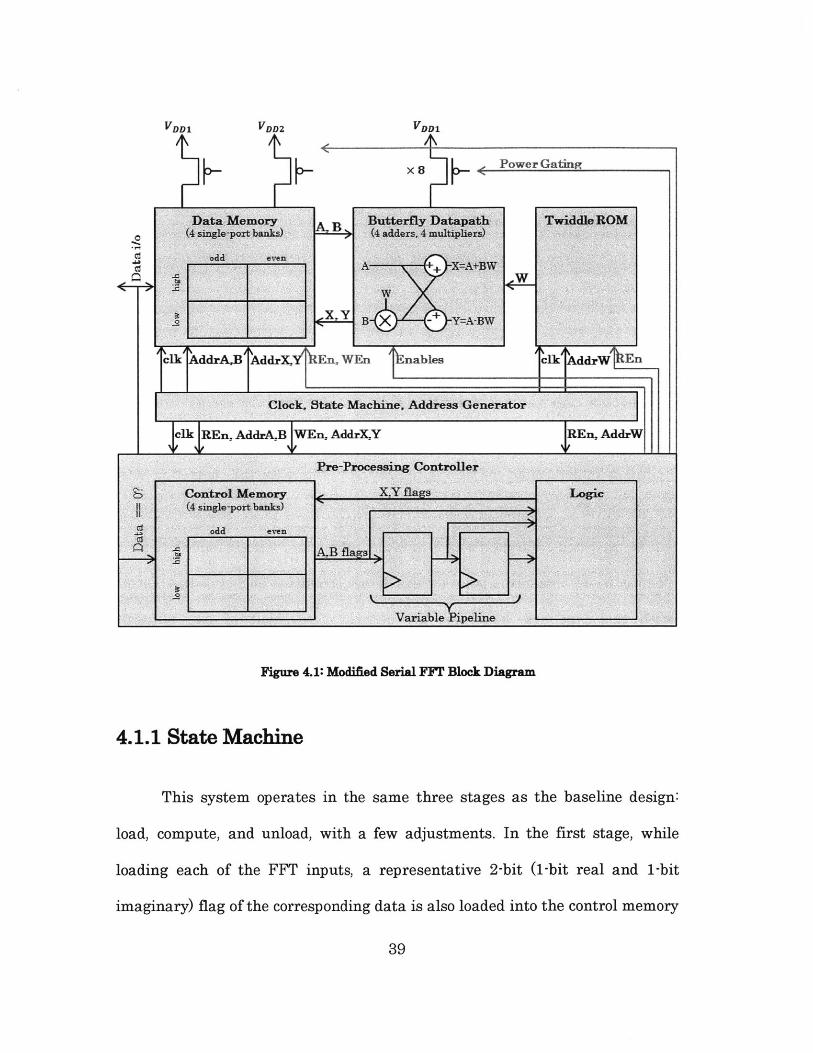
4.1.1 State Machine
This system operates in the same three stages as the baseline design:
load, compute, and unload, with a few adjustments. In the first stage, while
loading each of the FFT inputs, a representative 2-bit (1-bit real and 1-bit
imaginary) flag of the corresponding data is also loaded into the control memory
39
VDD1 VDD2
Data)Memory(4 single-port banks)
Odd even0
I
Butterfly Datapatli(4 adders, 4 multipliers)
W
Y=A-BW

simultaneously. The flag represents whether the corresponding data in the
memory is zero.
In the second stage, butterflies are computed in the same sequence, but with
additional energy-saving look-ahead logics that pre-fetch the corresponding
flags from the control memory and determine whether to read the data memory,
enable the adders and multipliers in the datapath, write back to the data
memory, power gate the datapath and voltage scale the data memory. There is
a trade-off between energy saved by a system in sleep and the energy consumed
to enter and exit the sleep state [9]. Thus, the design must consider future
iterations to determine the best optimizations. Bits from the control memory
are pipelined to the control logic, so that the workload of the future iterations
can be predicted. Through post layout and extraction Nanosim simulations in
Chapter 5, the break-even point for this design is found to be 2-cycle look-ahead.
With this pipelined structure, the original throughput of one butterfly
computation every clock cycle is maintained.
Upon completing all butterflies, the system enters the unaltered third stage to
unload the FFT frequency-domain results from data memory.
4.1.2 Control Memory
The control memory and data memory are initially populated
simultaneously using the same memory partitioning described in Section 3.2,
40

and thus share the same address locations and address generator for fetching
and updating data and flags during the compute phase.
A flag of "1" indicate that all bits of the corresponding data are zeros. At
every clock cycle, 5 flags are fetched and updated (written back to the control
memory): isOAr, isAi , isOBr, isOBi, islWr (equivalent to isO_Wi). The twiddle
factor flag is pre-determined based on the butterfly iteration count. Updated
flags are computed through a much simpler butterfly logic shown in Eq (4.1),
which is derived from Eq (3.2).
isOX, = isOYr = is0_Ar AND isOB, AND (islW, OR isOBi) (4. 1a)
isO_X- = isO Yi = isOAi AND (is1Wr OR isOB,) AND isOBi (4.1b)
4.1.3 Controller
Table 4.1 tabulates the control logic design variations to be implemented
and tested for energy savings comparison. Features such as disabling Memory
read/write (Mem Dis), disabling datapath (DP Dis), memory voltage scaling
(Mem VS), and datapath power gating (DP PG) are selectively implemented in
the tree operation stages. An energy savings comparison between the four
control logic variations are found in Section 5.2. The objectives are to compare
the datapath energy savings with the data memory energy savings and to
determine the optimum look-ahead amount.
41

Table 4.1: Four Variations of the Modified Serial Design Topologies
Look- Load Compute UnloadName Ahead -- -
cycles Mem Dis DP Dis Mem VS OP PG Mem Dis DP Dis Mem CG DP PG Mem Dis DP Dis Mem VS DP PG
Baseline - - - - - - - - - - -
Gated DP I 1 * * * 0 0 0
Gted DP 2 2 * * *
Gated 2Memory2 2* * . . * * ** * *
Gated 3Memory 3
In the load and unload stages, the datapath can be disabled to eliminate
unnecessary switching activity and reduce active energy. Power gating the
datapath can also reduce leakage energy. Unlike the compute stage, the critical
path is shorter without the datapath delay so the supply voltage to the memory
can be lowered from VDDl to VDD2 to further reduce energy. In the compute
stage, memory read and write can be disabled to save energy for the four
memory locations if predicted unnecessary (butterfly manipulations that will
result in no change to the data, data to be fetched is zero, etc). Memory supply
voltage can once again be lowered when the memory is disabled. The four
multipliers and four adders in the datapath can also be individually disabled
and power gated to save energy for cases such as multiply by 1 (WO twiddle
factors), multiply by 0 (low activity input data), or add 0.
Our overall contribution is a fully working low-energy pre-processing
controller not in the critical computation path that can predict the workloads of
future iterations and adjust the performance of the critical path accordingly.
This data-aware input-adaptive architecture is expected to save more energy as
42

the data becomes more intermittent or if a greater percentage of inputs are
zeros. As deliverables, plots of energy consumption as activity varies are shown
in Chapter 5 of the thesis.
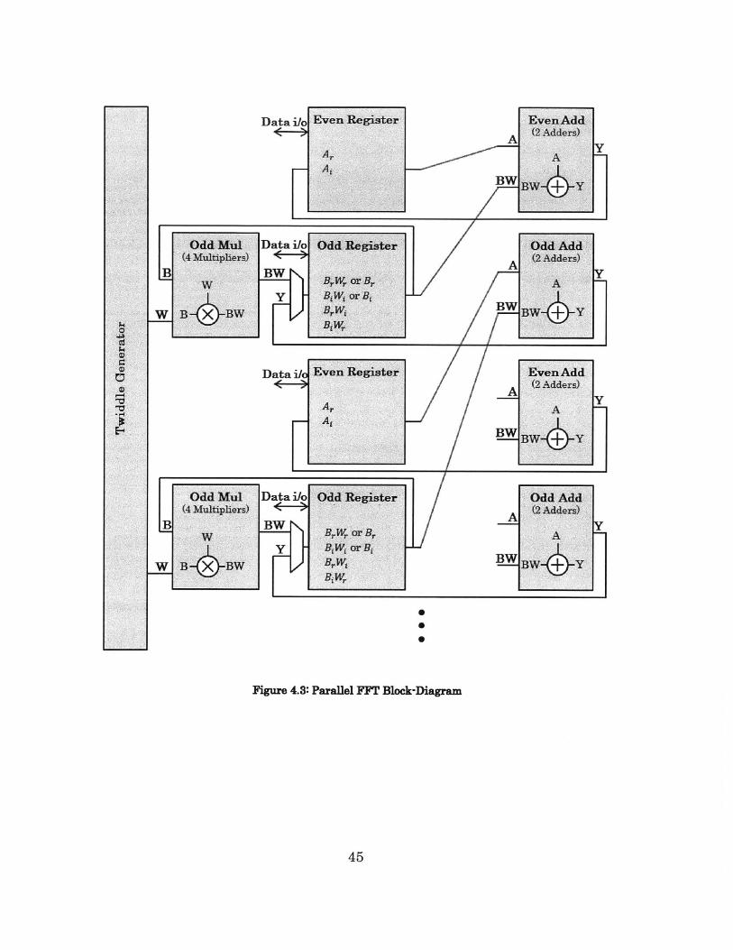
4.2 Parallel Architecture
This section proposes a parallel FFT architecture where all butterflies in
each stage are performed simultaneously. Again, a radix-2 decimation in time
FFT algorithm is used. This time however, a rearrangement of Figure 2.1 is
used to simplify data access. If each register continues to correspond to its
horizontal position in Figure 2.1, the inputs to the butterflies would have to
come from different positions for every new butterfly stages.
x101 X101
xt[4] S W S X(11
x[21 X(2]
W47 W1 WNx461 X[31
x[51 WM i W it Wm e ia1
x(31 1- X161
x[71 oWkX7
Figure 4.2: FFT Decimation in Time with Same Geometry in Each Stage [1]
43

As illustrated in Figure 4.2 above, each stage now has the same
geometry, which eliminates the dynamic routing complexity otherwise needed to
implement Figure 2.1. Instead of multiplexing large amount of data as inputs
to the butterflies for different stages, the same connections and logics can be
reused for all stages.
The block diagram of this parallel radix-2 FFT implementation is given
by Figure 4.3 below. Naturally, the parallel design is not restrained by serial
memory access, so the serial load and unload stages, the address generator, and
the four banks of memories that were used to store the butterfly results are no
longer necessary, thereby reducing energy. In this design, one set of internal
registers are used to store the intermediate calculated values at every stage.
The odd and even datapaths differ in that one consists of both the multi-cycle
multiply stage and the add stage, while the other only consists of the add stage.
The datapaths' inputs come from hardwired locations.
44
Data i/o
F-->B
W
Odd Mul I
Odd Mul(4 Multipliers)
w
W B _<XBW
Odd Register
B Wr or BrB7Wj
Data lc OdI~d
Data i/c, E )
Even Register
A
BW
EvenAdd(2 Adders)
A
BW
EvenAdd(2Adders)
A
BW +Y
Odd Add(2 Adders)
Bw4-i.Y
6
S
0
Figure 4.3: Parallel FFT Block-Diagram
45
Even Register
Odd Mul(4 Multipliers)
w
B X( BW
Odd Add(2 Adders)
BW- 4+Y
A
BW/
-4
1y
11
A
BW
Odd Register
Br W or B,BWor BiB aBiWr
A
Data i/b
J,
Data i/
.BW
Y
4.2.1 State Machine
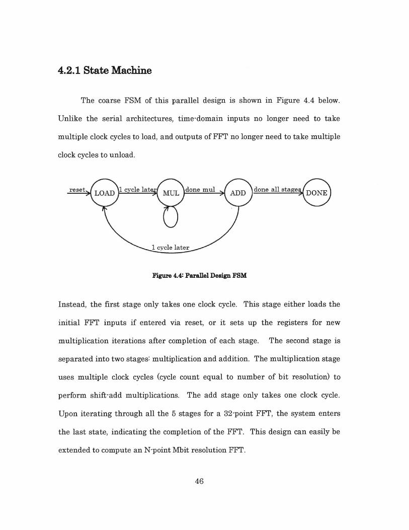
The coarse FSM of this parallel design is shown in Figure 4.4 below.
Unlike the serial architectures, time-domain inputs no longer need to take
multiple clock cycles to load, and outputs of FFT no longer need to take multiple
clock cycles to unload.
reset LOA 1 cycle lat done mul done all stage DONE
1 cycle later
Figure 4.4: Parallel Design FSM
Instead, the first stage only takes one clock cycle. This stage either loads the
initial FFT inputs if entered via reset, or it sets up the registers for new
multiplication iterations after completion of each stage. The second stage is
separated into two stages: multiplication and addition. The multiplication stage
uses multiple clock cycles (cycle count equal to number of bit resolution) to
perform shift-add multiplications. The add stage only takes one clock cycle.
Upon iterating through all the 5 stages for a 32-point FFT, the system enters
the last state, indicating the completion of the FFT. This design can easily be
extended to compute an N-point Mbit resolution FFT.
46

4.2.2 Implicit Memory
The implicit memory consists of odd and even registers. The even
registers are used to store A. The odd registers are much larger. These
registers are used to store either B or the four intermediate datapath
results BrWr, B*Wi, BrWi, and BiWr. From the block diagram in Figure 4.3, notice
that each data is computed in-place, and directly corresponds to its position in
the modified FFT flow chart in Figure 4.2. This memory structure allows the
same hard-wired inputs to the datapath at each stage, and eliminates
unnecessary dynamic routings. Differentiating between odd and even registers
also allows for a smaller design, since datapaths for even registers don't require
multipliers.
4.2.3 Datapath
The addition algorithm used for this design is straight forward, so this
section will focus on the multiplication algorithm. A pipelined multi-cycle shift-
add multiplier replaces the Design Ware multiplier from the serial design, and
is instantiated - times for the parallel design. By breaking the combinational2
logic down into smaller pipelined logic, the area of the design as well as the
propagation delay for each clock cycle (and hence the supply voltage needed) can
be reduced.
47

To multiply two 16-bit numbers, only 1 clock cycle is required by the
Design Ware multiplier, whereas 16 clock cycles are needed by this pipelined
multiplier. For each stage in the 32-point parallel FFT design, 16 butterflies
are computed simultaneously, and require 16 clock cycles to complete. For each
stage in the serial design, the 16 butterflies are computed sequentially, but also
take 16 clock cycles to complete. A net reduction in the total number of clock
cycles is still achieved by the parallel design, as loading and unloading data do
not require multiple clock cycles.
The Booth multiplication algorithm used in this design is a variation of
the simple shift-add algorithm. It handles multiplication of two signed numbers
in 2's complement representation by iteratively examining two adjacent pairs of
the multiplier's LSB every cycle [10]. Appendix C shows the actions needed for
each of the four LSB combinations, and an example of the Booth algorithm.
4.3 Modified Parallel Architecture
This section proposes a modified parallel FFT architecture where the
multi-cycle pipelined datapaths described in Section 4.2 are replaced with direct
instantiations of the baseline single-cycle combinational datapath. A fully-
parallel datapath where all the butterflies are unrolled is not considered here.
Again, the radix-2 decimation in time FFT algorithm in Figure 4.2 is
used. The block diagram of this modified parallel radix-2 FFT implementation
48
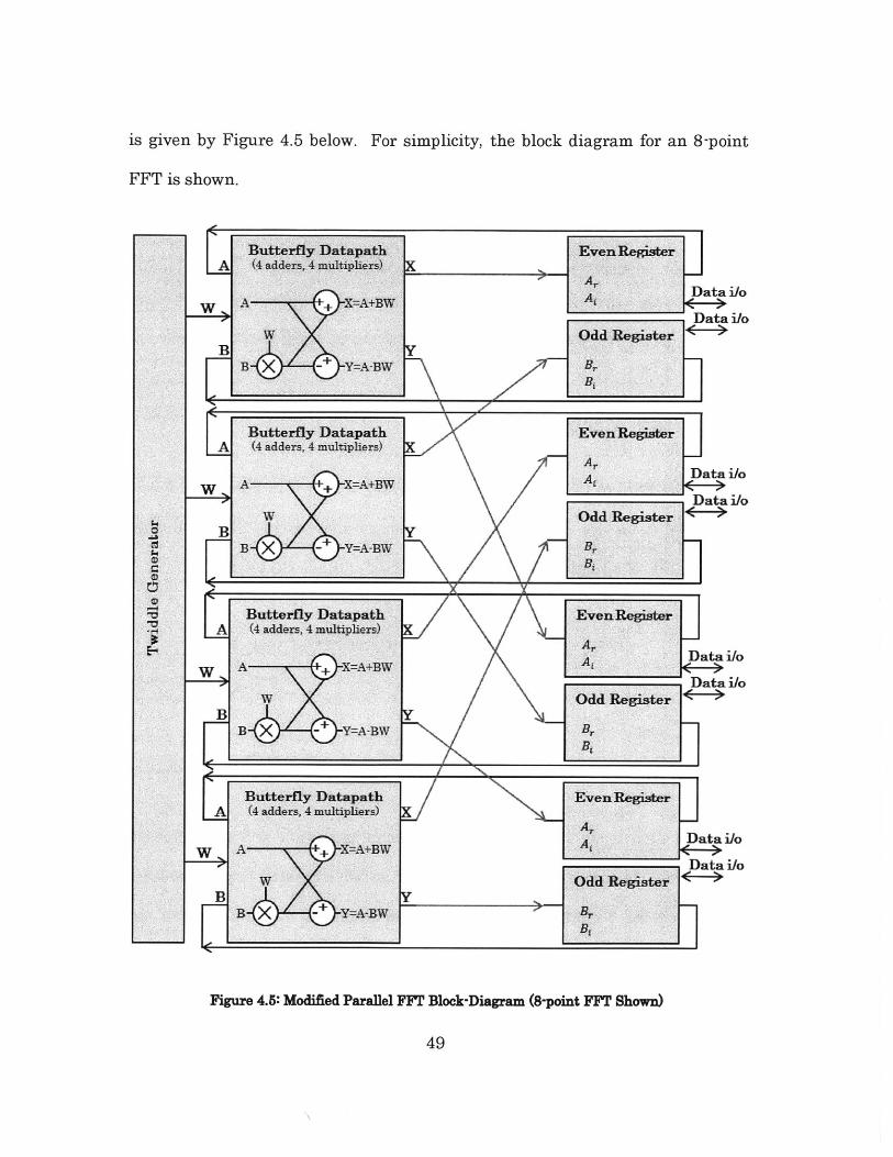
For simplicity, the block diagram for an 8-point
FFT is shown.
EvenRegister
Ar
Data i/oOdd Register
AhBIr
Butterfly Datapath(4 adders, 4 multiphers)
A '+ X=A+BW
W
B X - Y= -BW
Butterfly Datapath(4 adders, 4 multipliers)
A 4+ =A+BW
W
B a *y=A-BW
EvenRegisterx
A Datai/o
Data i/oOdd Register
Y IHr F
V V
I EvenRegisterx
YData i/o
Data i/oOdd RegisterC
YB,Bt
y
EvenRegister{]
AF Data i/o
Data i/oOdd Register
Br BII
Figure 4.5: Modified Parallel FFT Block-Diagram (8-point FFT Shown)
49
w
KButterfly Datapath(4 adders, 4 multiplers)
A +
W
B X - =-W
~2~ - 'a
Butterfly Datapath(4 adders, 4 multipliers)
A +" =A+BW
W
Ba _- Y= -BW
E-4
B
A
W
B
A
B
x V
is given by Figure 4.5 below.
As with the previous parallel architecture, this design is not restrained
by serial memory access, so the serial load and unload stages, the address
generator, and the four banks of memories that were used to store the butterfly
results are no longer necessary. Since the datapath is no longer split into multi-
cycle multiplication and add, the odd registers no longer need to be large enough
to accommodate the intermediate products BrWr, BLW, BrW, and BiWr.
4.3.1 State Machine
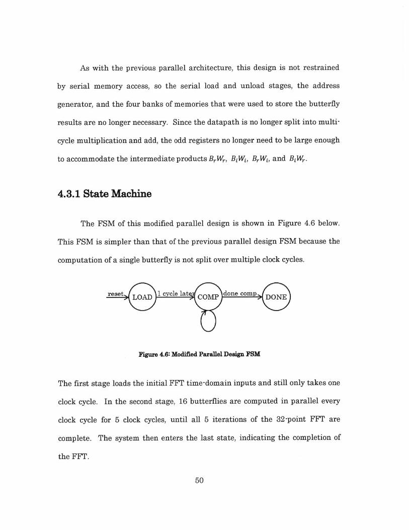
The FSM of this modified parallel design is shown in Figure 4.6 below.
This FSM is simpler than that of the previous parallel design FSM because the
computation of a single butterfly is not split over multiple clock cycles.
reset LOD1 cycle 1a CM done comp DN
Figure 4.6: Modified Parallel Design FSM
The first stage loads the initial FFT time-domain inputs and still only takes one
clock cycle. In the second stage, 16 butterflies are computed in parallel every
clock cycle for 5 clock cycles, until all 5 iterations of the 32-point FFT are
complete. The system then enters the last state, indicating the completion of
the FFT.
50
4.3.2 Implicit Memory
The implicit memory consists of even and odd registers used to store A
and B, respectively. The outputs of these registers are directly fed into the
corresponding butterfly. Each data is computed in-place, and directly
corresponds to its position in the modified FFT flow chart in Figure 4.2. This
memory structure allows the same inputs to the datapath at each stage, and
eliminates unnecessary dynamic routings. Unlike the previous parallel design,
no differentiation between odd and even registers is really necessary except for
differentiating between the A and B butterfly port connections.
4.3.3 Datapath
This design uses the same datapath as that of the baseline design, only
instantiated multiple times. The use of a single-cycle datapath greatly reduces
the number of clock cycles needed to compute the FFT. Only 10Y2 3 2 = 5 clock
cycles are needed to compute the 32-point FFT, which is of that used by the16
previous parallel design. Given a fixed requirement on the FFT completion
time, the frequency of the clock can be greatly reduced which allows the supply
voltage to be scaled lower. This along with the reduction in register count all
contribute to a significant reduction in energy consumption.
51

52

Chapter 5
Simulation Results
In this chapter, the simulation results will be presented to evaluate the
effects of parallelism and data-dependency on energy. The tools and simulation
flow are introduced first, followed by a quantitative comparison of the designs.
All the simulation results are from post-layout and parasitic Nanosim
simulations. The test cases include varying the percentages of zero-data for
different FFT performance requirements.
5.1 Tools and Simulation Flow
Each design (baseline, modified serial (x4), parallel, and modified
parallel) follow the design and simulation flow summarized in Table 5.1 below.
They are carried out from RTL design through to synthesis and place and route.
Matlab is used to create the golden model and to assist with the verification of
53

the designs. The technology used to generate the simulation results in this
Chapter is the generic 90nm Cadence gpdk09O process.
Table 5.1: Tools, Simulation and Design Flow
Flow Tools Outputs generated1. RTL Simulation Cadence NC Verilog .txt (simulation outputs)
(functional simulation tooh .vcd (simulation waveforms)
2. RTL Debugging Cadence SimVision .txt (golden model(viewing digital waveforms)
Matlab(numerical computingenvironment)
3. Synthesis Cadence RC .rpt (synthesis log lies)(synthesis tooh .v (synthesized gate netlist)
4. Define Power .cpf (define power domains)
Domains5. Place and Route Cadence Encounter .gds (chip layout details)
(place and route tooh .v (gate netlis)
Reports6. DRC, LVS, and Cadence Virtuoso .sp (spice netlist containing
Parasitic Extraction (custom IC design tooh parasitics)
7. Generate Input Nanosim .vec (input vectors for
Vectors (power simulation tooh testbench)
8. Post Layout Nanosim Reports (containing power
Simulation CScope info)(viewing digital and analog .fsdb (simulation waveforms)waveforms)
For each of the designs, the corresponding SPICE netlist generated in
step 6 is used in conjunction with different combinations of ".vec" vector files
and ".sp" test benches for the Nanosim simulations. The lowest power and
energy associated with each design are evaluated for the matrix of test cases
summarized in Table 5.2.
54

Table 5.2: Test Cases
M odified Parallel FFTParallel FFT
Modified Serial FFTBaseline Serial FFT Percent of Zero-Data
Ozero -~6zero l2zero 24zero 36zero 4zero 60zero 64zero0% 9.375% 18.75% 37.5% 56.25% 75% 93.75% 100%
S4280ns.**!E 2140ns * - -.
0 1760ns
Covering all these test cases is an iterative process. For a given design and a
given FFT completion time requirement, the associated clock frequency for that
design is calculated and set in the Verilog test bench. The Ozero test case is the
default, and the simulation is run in step 1 to generate the ".vcd" simulation
waveform. Step 7 is then performed to convert the ".vcd" file into a ".vec" file
using Nanosim's vcd2vec command. Next, the supply voltage is set to the
nominal 1.2V in the .sp test bench and then Nanosim is run in step 8 to
generate the ".fsdb" simulation waveform. The waveform is viewed in CScope to
confirm correct functionality. To determine the lowest working supply voltage,
the supply voltage is incrementally lowered and the simulation is rerun until
the waveform is no-longer correct. Step 1 and 7 are then repeated for different
percentages of zero-data inputs, and the various ".vec" files are used with the
minimum supply voltage to perform Nanosim simulations in step 8. This entire
process is rerun for the different architectures. Just to reiterate, all the designs
are functional and produce the same FFT results as the baseline design.
55

5.2 Modified Serial vs. Baseline
This section compares the post layout (with standard cell blocks) and post
parasitic extraction Nanosim simulation results between the four variations of
the modified serial design and the baseline design for computing a 32-point
FFT. The energy comparisons are based on the test case with a fixed FFT
completion time of 4280ns. For the serial design, this corresponds to a clock
frequency of 50MHz and a minimum supply of VDD1 = 0.6V and VDD2 = 0.5V.
Note that due to the lack of readily available SRAM in gpdk090, flip-flop based
memories are used instead. With SRAM, similar energy savings are expected.
Figure 5.1 and Figure 5.2 below show the simulation results of the energy
per FFT for the four designs compared to the baseline design (with no pre-
processing controller), given various proportions of input zeros. Figure 5.1 is a
point-by-point normalization of the new designs to the baseline design. In this
normalization scheme, for each percentage of zeros considered, the normalized
energy per FFT is calculated by Energy per EFT for design XEnergy per FFT for baseline evaluated at a given % of zero
The baseline curve for this normalization is always flat at 1. The point-by-point
normalization scheme provides a clear comparison and easy evaluation of the
relative percentage of energy savings for various proportions of zeros. Figure
5.2 on the other hand is a normalization of the new designs to the highest
energy point of the baseline design. In this normalization scheme, for each
percentage of zeros considered, the normalized energy per FFT is calculated by
56
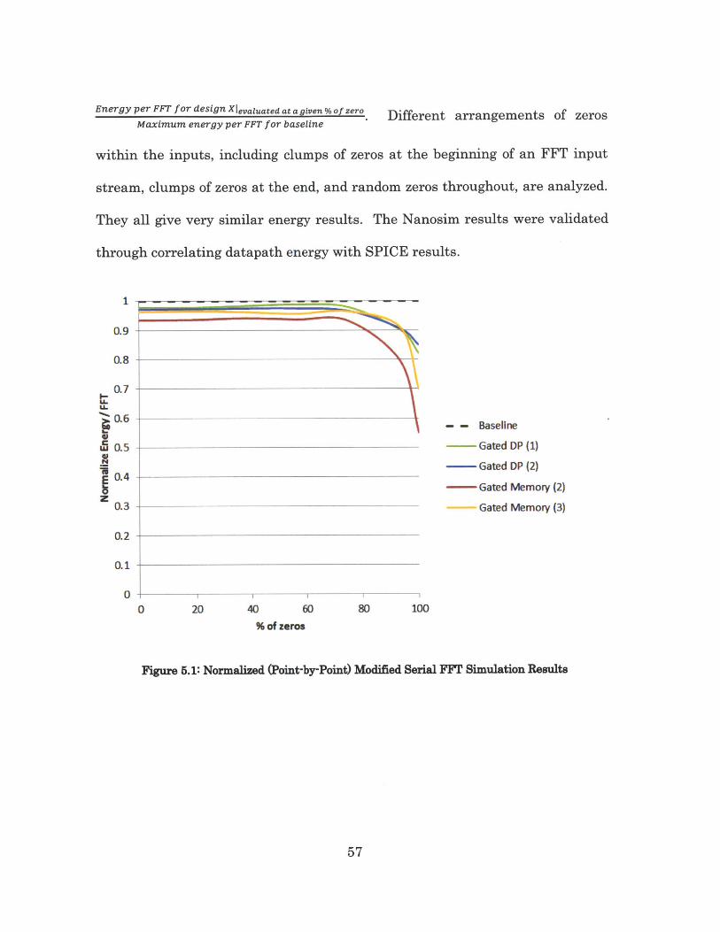
Energy per FFT for design XIevaluated at a given % of zero fliffprpnt. ~ of zz~voi~Maximum energy per FFT for baseline
within the inputs, including clumps of zeros at the beginning of an FFT input
stream, clumps of zeros at the end, and random zeros throughout, are analyzed.
They all give very similar energy results. The Nanosim results were validated
through correlating datapath energy with SPICE results.
1
0.9
0.8
0.7
a.6
a 0.5
0.4
Z0.3
0.2
0.1
0
---
- - Baseline
Gated DP (1)
--- Gated Do (2)
- Gated Memory (2)
......... ,Gated Memory (3)
0 20 40 60
% of zeros80 100
Figure 5.1: Normalized (Point-by-Point) Modified Serial FFT Simulation Results
57
\ It
1
0.9
0.8
0.7U-U-
0.6
w 0.5
E 0.4L-0z
0.3
0.2
0.1
0
20 40 60
% of zeros80 100
Figure 5.2: Normalized (Highest-Point) Modified Serial FFT Simulation Results
The four design variations are defined in Table 4.1. The "gated DP (1)"
design has control logics that can disable the data memory, datapath, or ROM,
and power gate the datapath based on the workload on each clock cycle. Second,
the "gated DP (2)" design has control logics that can adjust the handles in the
first design if the workload is low for the next 2 clock cycles. Third, the "gated
memory (2)" design has control logics that can clock/power gate the data
memory in addition to adjusting the handles in the second design if the
workload is low for the next 2 clock cycles. Fourth, the "gated memory (3)"
design has control logics that can adjust the handles in the third design if the
workload is low for the next 3 clock cycles.
58
- - Baseline
Gated DP (1)
-- Gated DP (2)
-- Gated Memory (2)
Gated Memory (3)
0

In all four cases, for <75% zeros, the four designs save 3-7% total energy
from small savings in power gating the datapath when loading/unloading the
data memory. The small energy savings for highly-non-zero data is likely due to
the fact that the low-power techniques such as clock gating, power gating,
memory read and write disabling, and voltage scaling were not utilized often.
For these cases, the overhead energy of the pre-processing controller still offsets
the energy savings from disabling the butterfly datapaths during the FSM's
load and unload stages. Savings become significant for >75% zeros. The gated
datapath designs save ~7% total energy for 90% zeros. The significant energy
savings for highly-zero data is likely due to the fact that the low-power
techniques are utilized most of the time. As most of the data is zero, memory
access and leakage is limited. The effect of zeros at the input is propagated
down the chains of butterflies. If the majority of data is zero to begin with, the
majority of data will continue to stay zero for most of the butterflies in later
stages, thus energy savings will continue after the first stage. If only a minority
of data is zero however, the data of the butterflies in later stages are unlikely to
stay zero after datapath manipulations with non-zero data, thus energy savings
are only likely during the first stage.
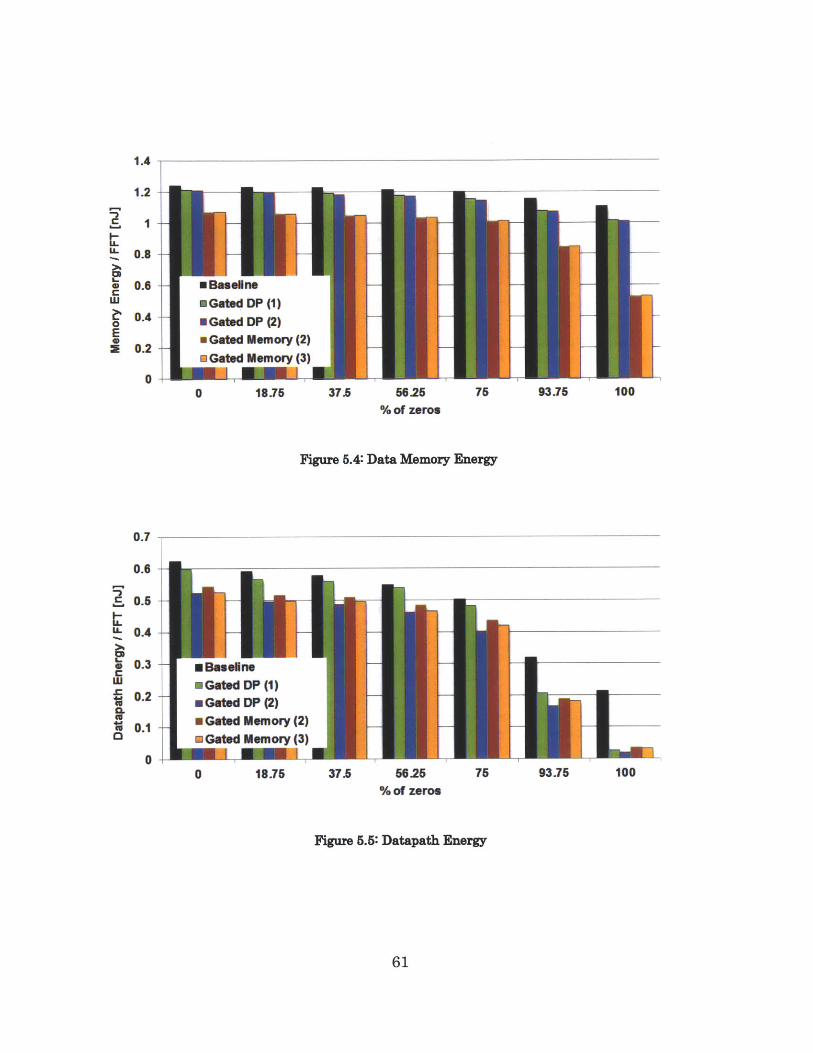
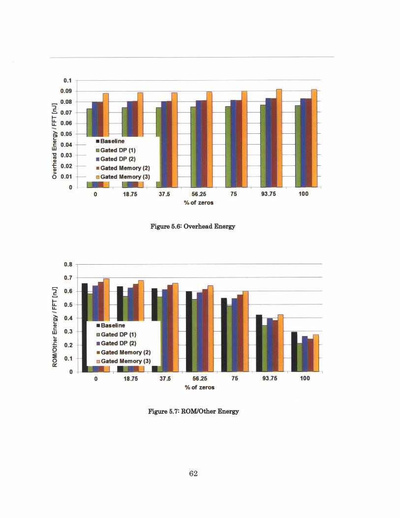
Figure 5.4, Figure 5.5, Figure 5.6, and Figure 5.7 compare the breakdown
of the energy consumed by the data memory, datapath, controller, and
ROM/others, respectively for the baseline and the four modified designs. These
energy breakdowns are again extracted from post-layout and parasitic
59

extraction Nanosim simulations. In all four designs, greater energy savings is
achieved with more input zeros since the system blocks sleep more often.
Clock/power gating the data memory in addition to the datapath saves 3 times
the energy as gating the datapath alone. This is consistent with Figure 5.3,
which shows that the data memory consumes twice the energy (~50% total) of
the datapath (~25%) per FFT. The gated memory designs save 5-40% of total
energy in reducing clock transitions and leakage energy in the data memory.
Much datapath energy is saved between the 2-cycle and 1-cycle look-ahead
designs (5-10% vs. 1-10%), but very little is saved between 3-cycle and 2-cycle.
The 2-cycle look-ahead saves more energy than 1-cycle look-ahead due to its
lower overhead and since the system is sleeping often. The 3-cycle look-ahead
variation saves less energy than 2-cycle due to overhead for small marginal
savings. Thus, the optimal design is found to be the 2-cycle look-ahead gated
memory and datapath through Nanosim simulations
Baseline Gated Memory (2)
-i ROM/Other
49% Datapath 45%
Memory
a Overhead
Figure 5.3: Energy Breakdown of Blocks in Serial FFT Systems (Ozero)
60
aBaselne
" Gated DP (1)" Gated DP (2)" Gated Memory (2)" Gated Memory (3)
0 18.75 37.6 56.26 76% of zeros
Figure 5.4: Data Memory Energy
E BaselneE Gated DP (1)Gated DP(2)
m Gated Memory (2)EGated Memory (3)
18.75 37.6 56.26%of zeros
76 93.75 100
Figure 5.5: Datapath Energy
61
1.4
1.2
U-U-
LK
0E
0.8
0.6 +0.4 ±0.2
93.75 100
0.7 7
0.6
0.6
0.4--
0.3
0.2
0.1
UJ
w
00
-1
0.1
0.09 ----
0.08
0.07
U 0.06
0.05
a 0.04 - maselneSm Gated DP (1)
0 Gated DP (2)0.02 n Gated Memory (2)
o 0.01 - s Gated Memory (3)
00 18.75 37.5 56.25 75 93.75 100
% of zeros
Figure 5.6: Overhead Energy
0.8
0.7
0.6 _
0.5
0.4* EBaselneU 0.3 * Gated DP (1)
E 0.2 m Gated DP (2)-- a Gated Memory (2)0 0.1 r Gated Memory (3)
0 -0 18.75 37.5 56.25 75 93.75 100
% of zeros
Figure 5.7: ROM/Other Energy
62
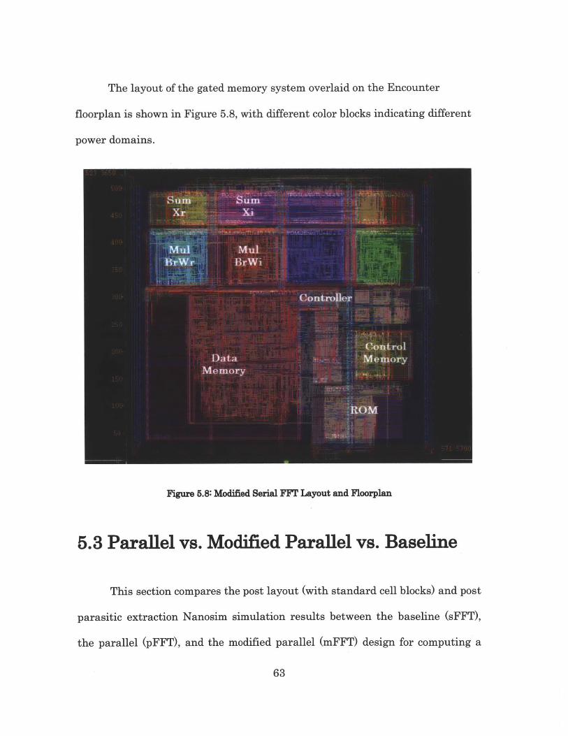
The layout of the gated memory system overlaid on the Encounter
floorplan is shown in Figure 5.8, with different color blocks indicating different
power domains.
Figure 5.8: Modified Serial FFT Layout and Floorplan
5.3 Parallel vs. Modified Parallel vs. Baseline
This section compares the post layout (with standard cell blocks) and post
parasitic extraction Nanosim simulation results between the baseline (sFFT),
the parallel (pFFT), and the modified parallel (mFFT) design for computing a
63
32-point FFT. The energy comparisons are based on the test cases with the
corresponding clock frequency and minimum supply voltage summarized in
Table 5.3.
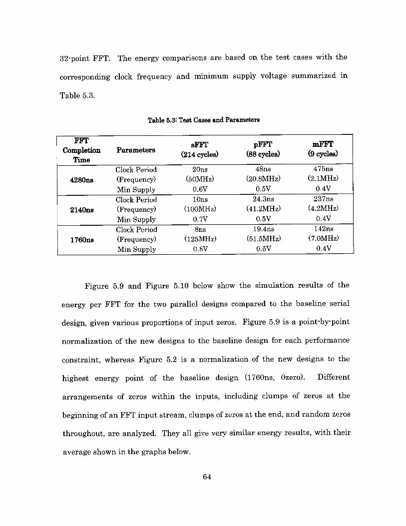
Table 5.3: Test Cases and Parameters
C pt PFT pFFT mFFTCompletion Parameters (214 cycles) (88 cycles) (9 cycles)
TimeClock Period 20ns 48ns 475ns
4280ns (Frequency) (50MHz) (20.8MHz) (2.1MHz)Min Supply 0.6V 0.5V 0.4V
Clock Period iOns 24.3ns 237ns
2140ns (Frequency) (100MHz) (41.2MHz) (4.2MHz)Min Supply 0.7V 0.5V 0.4V
Clock Period 8ns 19.4ns 142ns
1760ns (Frequency) (125MHz) (51.5MHz) (7.0MHz)Min Supply 0.8V 0.5V O.4V
Figure 5.9 and Figure 5.10 below show the simulation results of the
energy per FFT for the two parallel designs compared to the baseline serial
design, given various proportions of input zeros. Figure 5.9 is a point-by-point
normalization of the new designs to the baseline design for each performance
constraint, whereas Figure 5.2 is a normalization of the new designs to the
highest energy point of the baseline design (1760ns, Ozero). Different
arrangements of zeros within the inputs, including clumps of zeros at the
beginning of an FFT input stream, clumps of zeros at the end, and random zeros
throughout, are analyzed. They all give very similar energy results, with their
average shown in the graphs below.
64
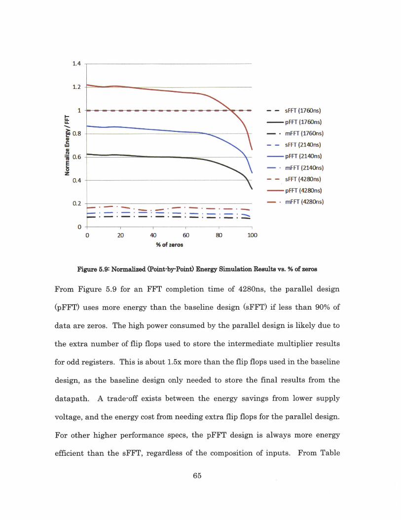
1.4
F- -
-MM - N -.. --..-
80 100
% of zeros
Figure 5.9: Normalized (Point-by-Point) Energy Simulation Results vs. % of zeros
From Figure 5.9 for an FFT completion time of 4280ns, the parallel design
(pFFT) uses more energy than the baseline design (sFFT) if less than 90% of
data are zeros. The high power consumed by the parallel design is likely due to
the extra number of flip flops used to store the intermediate multiplier results
for odd registers. This is about 1.5x more than the flip flops used in the baseline
design, as the baseline design only needed to store the final results from the
datapath. A trade-off exists between the energy savings from lower supply
voltage, and the energy cost from needing extra flip flops for the parallel design.
For other higher performance specs, the pFFT design is always more energy
efficient than the sFFT, regardless of the composition of inputs. From Table
65
- - sFFT (1760ns)
pFFT (1760ns)
-- - mFFT(1760ns)
- - sFFT (2140ns)
pFFT (2140ns)
-- -mFFT(2140ns)
sFFT (4280ns)
pFFT (4280ns)
-- - mFFT (4280ns)
1.2
1U-UL
90.8
0.6Ez
0.4
0.2
00 20 40 60

5.3, there is a small supply voltage difference of 0. 1V between the parallel
design and the baseline design for FFT completion time of 4280ns. However, a
larger supply voltage difference of 0.2V and 0.3V exists for the lower
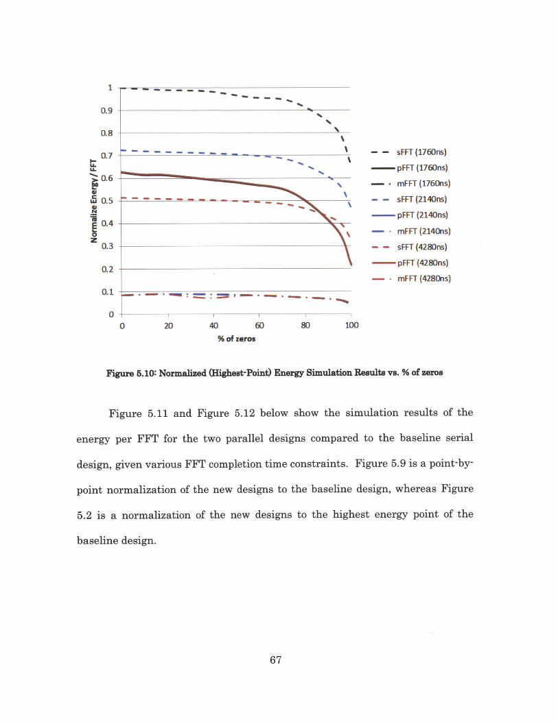
performance spec of 2140ns and 1760ns, respectively, likely resulting in the
more fruitful energy savings observed. For all simulated completion time, the
modified parallel design (mFFT) uses an order of magnitude lower energy
compared to the baseline design, regardless of the inputs. Such a great
reduction in energy consumption is likely due to the fact that the supply voltage
can be lowered to near-threshold voltage, since the low cycle count allow for a
much slower clock. The modified parallel design also does not need the extra
flip-flops that the parallel design needed, as only the final datapath results are
stored.
66
1
0.9
0.8
0.7
0.6
0.5
0.4
0.3
0.2
0.1
0
- -.- 1.
___ __ ---- _
- 4
"" ~ ~ ~ Mo W W- - ' - - .
- - sFFT (1760ns)
pFFT (1760ns)
- - mFFT (1760ns)
- - sFFT (2140ns)
pFFT (2140ns)
-- - mFFT (2140ns)
- - sFFT (4280ns)
pFFT (4280ns)
-- - mFFT (4280ns)
0 20 40 60 80 100
% of zeros
Figure 5.10: Normalized (Highest-Point) Energy Simulation Results vs. % of zeros
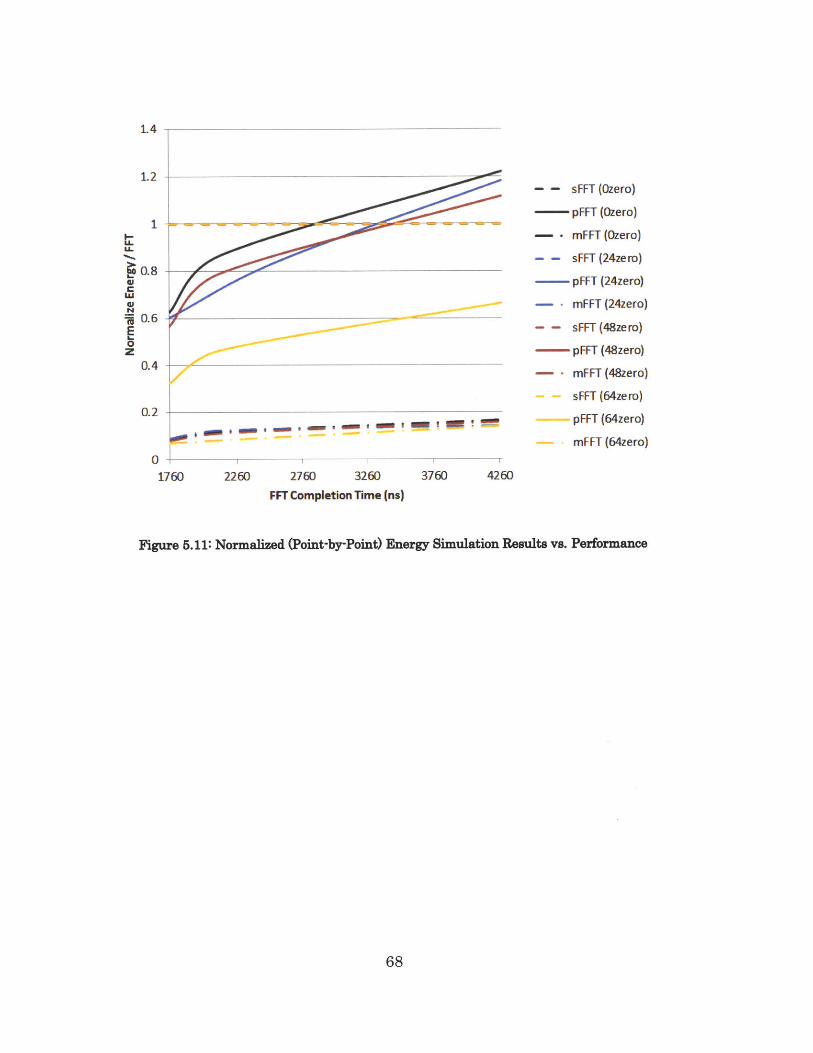
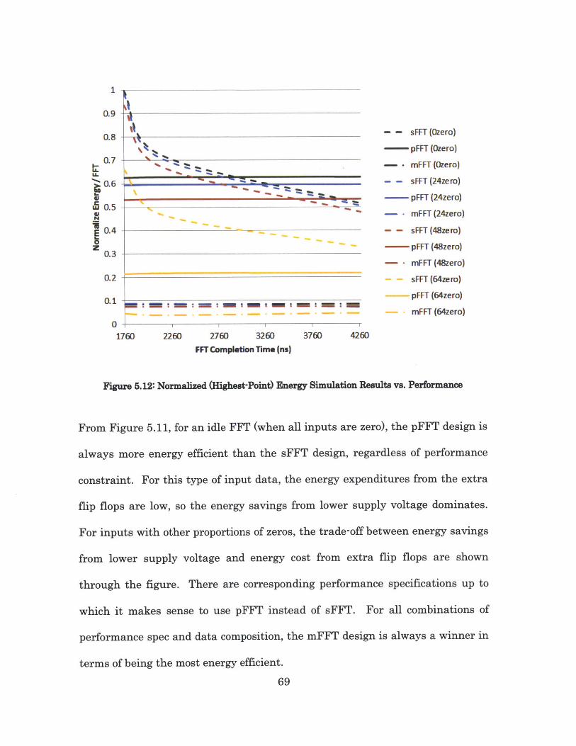
Figure 5.11 and Figure 5.12 below show the simulation results of the
energy per FFT for the two parallel designs compared to the baseline serial
design, given various FFT completion time constraints. Figure 5.9 is a point-by-
point normalization of the new designs to the baseline design, whereas Figure
5.2 is a normalization of the new designs to the highest energy point of the
baseline design.
67
E0N
. t 4 - I - t - ..
- - sFFT (Ozero)
pFFT (Ozero)
- mFFT (Ozero)
- - sFFT (24zero)
pFFT (24zero)
- mFFT (24zero)
- - sFFT (48zero)
pFFT (48zero)
- -mFFT (48zero)
sFFT (64ze ro)
pFFT (64zero)
mFFT (64zero)0
1760 2260 2760 3260
FFT Completion Time (ns)
Figure 5.11: Normalized (Point-by-Point) Energy Simulation Results vs. Performance
68
1.4
1.2
1
U-
S40.8
ILl
M0.6E0z
0.4
n 1)
---- -
3760 4260
1
0.9
0.8
0.7
0.6
0.5
0.4
0.3
0.2
01mFFT(64zero)
01760 2260 2760 3260 3760 4260
FFT Completion lime (na)
Figure 5.12: Normalized (Highest-Point) Energy Simulation Results vs. Performance
From Figure 5.11, for an idle FFT (when all inputs are zero), the pFFT design is
always more energy efficient than the sFFT design, regardless of performance
constraint. For this type of input data, the energy expenditures from the extra
flip flops are low, so the energy savings from lower supply voltage dominates.
For inputs with other proportions of zeros, the trade-off between energy savings
from lower supply voltage and energy cost from extra flip flops are shown
through the figure. There are corresponding performance specifications up to
which it makes sense to use pFFT instead of sFFT. For all combinations of
performance spec and data composition, the mFFT design is always a winner in
terms of being the most energy efficient.
69
U-
EbZ H~
- - sFFT (Ozero)
pFFT (Ozero)
- - mFFT (Ozero)
- - sFFT (24zero)
pFFT (24zero)
-- mFFT (24zero)
- - sFFT (48zero)
pFFT (48zero)
-- -mFFT (48zero)
sFFT (64zero)
pFFT (64zero)
IL
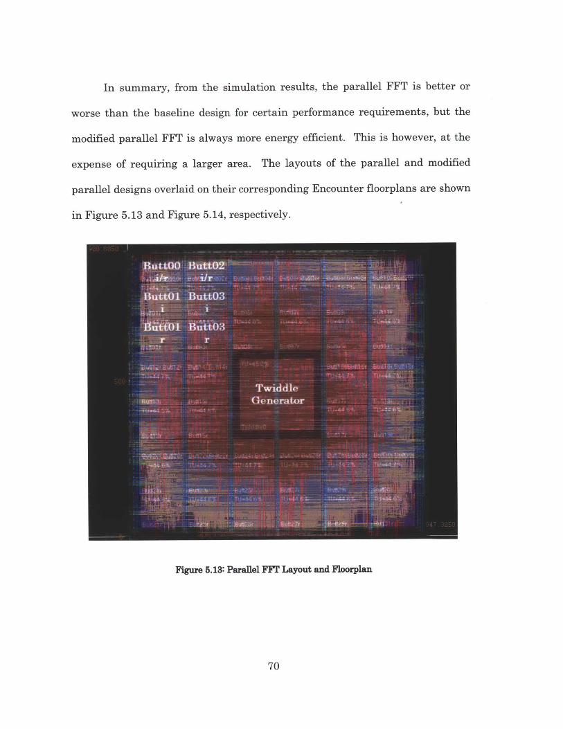
In summary, from the simulation results, the parallel FFT is better or
worse than the baseline design for certain performance requirements, but the
modified parallel FFT is always more energy efficient. This is however, at the
expense of requiring a larger area. The layouts of the parallel and modified
parallel designs overlaid on their corresponding Encounter floorplans are shown
in Figure 5.13 and Figure 5.14, respectively.
Figure 5.13: Parallel FFT Layout and Floorplan
70
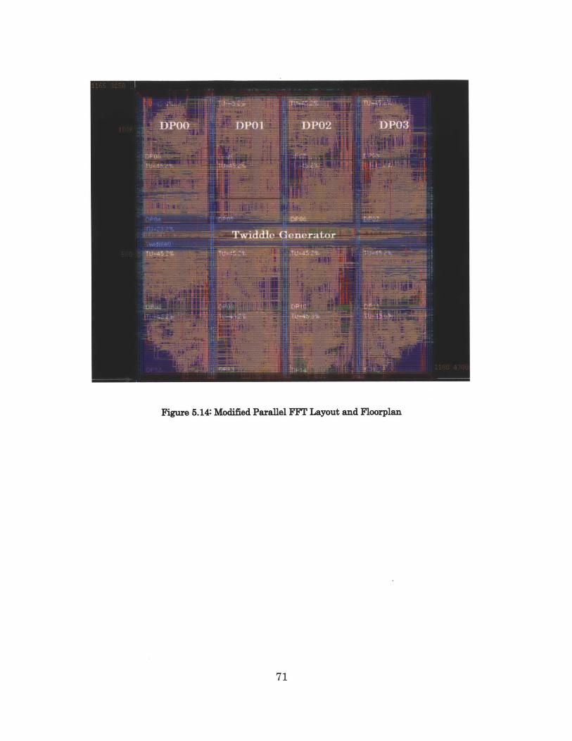
Figure 5.14: Modified Parallel FFT Layout and Floorplan
71

72
Chapter 6
Conclusions
This thesis explored several new 32-point radix-2 FFT architectures that
take advantage of data dependency and parallelism to save energy. In
summary, the modified serial architecture and the modified parallel
architecture can reduce the energy per FFT by up to 45% and 90%, respectively,
when compared to the baseline design.
For the modified serial design, the ideas of dynamically optimizing energy
within each FFT (as opposed to between FFT computations), regulating a large
data memory with a small representative control memory, and designing a
controller that looks ahead at a sequence of input data to determine the best
optimization for the next iteration are pursued. The overall contribution is a
fully working low-energy pre-processing controller not in the critical
computation path that can predict the workloads of future iterations and adjust
73

the performance of the critical path accordingly. A low-voltage control memory
is incorporated that stores one bit for each 16-bit word in the data memory
indicating whether it is zero. The control logic determines the workload
required in each iteration based on how many inputs are zero, and then
disables/voltage-scales the data memory, disable/power gates the datapath, or
disables the ROM. Bits from the control memory are pipelined to the control
logic so it can consider the workload of future iterations. Through Nanosim
simulations of four variation of the design, the 2-cycle look-ahead gated memory
and datapath design appeared to be the most optimal.
For the parallel and modified parallel design, the idea of basing the
parallel architecture on a different flow graph, where each stage is completely
identical is pursued. This can eliminate the need for routing large amounts of
data dynamically for each new butterfly stage. The overall contribution is a
fully working parallel architecture. The datapath of the modified parallel
design is simply multiple instantiations of the datapath from the baseline
design. Through Nanosim simulations, it is demonstrated that the single-cycle
arithmetic unit is indeed better than the multi-cycle heavily pipelined
arithmetic unit. This is because the fewer cycle count allows for the clock
frequency to be greatly reduced, which in turn allow for a reduction in supply
voltage.
Note that due to the lack of readily available SRAM in gpdk09O, flip-flop
based memories are used instead. Future work could include incorporating the
74

SRAM into the modified serial FFT design to see its impact on energy savings.
For small storage capacity, such as the case for 32-point FFT, the overhead of
SRAM's peripheral circuitry such as the precharge circuitry and sense amplifier
may lead to bigger area and possibly more energy consumption compared to flip -
flop based memories [14]. However, similar relative energy savings are still
expected from the modified serial design when compared to the baseline deign.
It is also recommended that further exploration is done on different parallel
implementations. Particularly, as recommended by Professor Chandrakasan, a
fully expanded parallel architecture, where all FFT butterflies are performed
simultaneously (as opposed to only the ones in the same stage) could be
developed. In this scheme, dedicated hard-wired multipliers and adders could
be developed for different twiddle factors. This is in contrast with the generic
multipliers used in all the datapaths within this thesis. Lastly, only the energy
savings for N=32 (32-point FFT) were explored here. It would be interesting to
see if such energy savings continue to scale with higher-point FFT (e.g. 1024-
point FFT). For higher-point FFT, bigger relative energy saving is expected
from the modified serial design as the energy savings from the data memory
and datapath becomes more dominant over the cost of the controller overhead
energy. For the modified parallel design, greater relative energy saving is also
expected, as the cycle count ratio between the modified parallel design and
baseline design, log 2 N : N 1og 2N, continues to diminish. The bigger frequency
differences allow more differences between the supply voltages.
75

76

Appendix A
Alternative Forms of FFT
Flow Diagrams
x[1] >X[4]
4211x[2) -X[2]
x[3]J{6
x[6] X I]
WnW
x[7] & - X[71
Figure A.1: FFT Decimation-in-Time with Input in Normal Order [1]
77
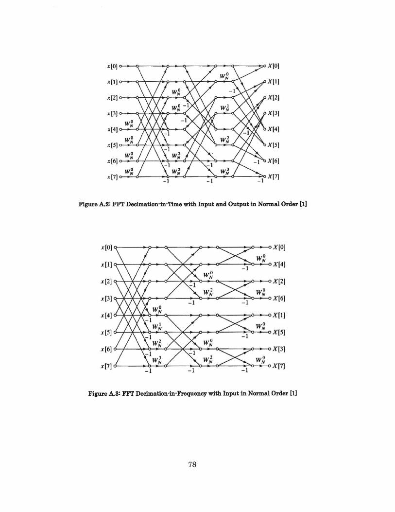
WIVO X[l]
WIx [21 X(21
x[3 X31
WO
x(5) 5]X5
x[6 X61
7 W N N N X171
Figure A.2: FFT Decimatio-in-Time with Input and Output in Normal Order [1]
x 10] %6nb- X[0]
WJOW
W,2
W WNx[3] X[6]
x[41 -+-o X[1]
x[65] X[313
-x[7] ! N WI -X[3]
Figure A.$: FFT Decimation-in-Frequency with Input in Normal Order [1]
78

Appendix B
Baseline Implementation
Details
Table B.1: Input Ordering vs. Address Locations of an 8-point FFT
FFT inputs N address k FFT outputsx[n] in binary (bit-reversed n) Xk]x[0] 000 000 X[0]x[4] 100 001 X[]x[2] 010 010 X[2]x[6] 110 011 X[3]x[1] 001 100 X[4]x[5] 101 101 X[5]x[3] 011 110 X[6]x[7] 111 111 X[7]
79
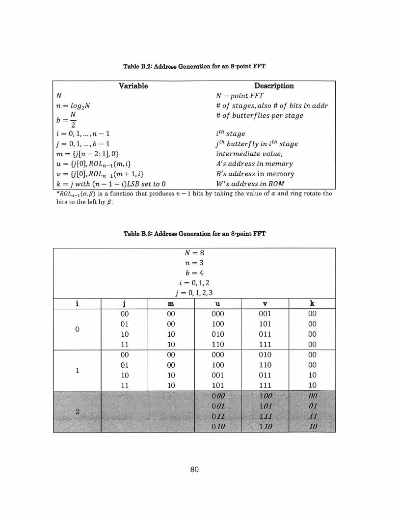
Table B.2: Address Generation for an 8-point FFT
VariableNn = 1og 2N
Nb = N_
2i =0, 1, ...,n - 1
j =0, 1, ...,b - 1m = U[n - 2: 1], 0}u = fj[0], ROLn_ 1(m, i)v = {j[0], ROLn_ 1(m + 1, i}k =]with (n - 1 - i)LSB set to 0
DescriptionN - point FFT# of stages, also # of bits in addr# of butterflies per stage
ith stage
jtt butterf ly in ith stageintermediate value,A's address in memoryB's address in memoryW's address in ROM
*ROL_ 1 (a, fl) is a function that produces n - 1 bits by taking the value of a and ring rotate thebits to the left by p.
Table B.3: Address Generation for an 8-point FFT
N =8n =3b =4
i = 0, 1, 2j = 0, 1, 2,3
i m u v k00 00 000 001 00
0 01 00 100 101 0010 10 010 011 0011 10 110 111 00
1
00011011
00001010
000100001101
010110011111
00001010
80

Appendix C
Booth Multiplier Algorithms
Table C.1: Booth Algorithm LSB Combinations [11
LSB Action00 1. Do nothing
2. Shift product to the right (sign extend MSB)01 1. Add product by multiplicand (ignore any overflow)
2. Shift product to the right (sign extend MSB)10 1. Subtract product by multiplicand (ignore any overflow)
2. Shift product to the right (sign extend MSB)11 1. Do nothing
2. Shift product to the right (sign extend MSB)
81
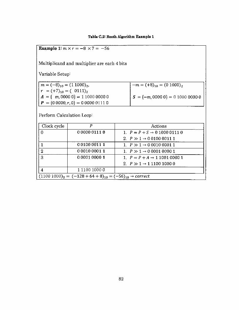
Table C.2: Booth Algorithm Example 1
m = (-8)10 = (1 1000)2, -m = (+8)10 = (0 1000)2r = (+7)10 = ( 0111)2A = f m, 0000 0} = 1 1000 0000 0 S = f-m, 0000 0} = 0 1000 0000 0P = {0 0000,r,O) = 0 0000 0111 0
Perform Calculation Loop:
Clock cycle P Actions0 0000001110 1. P=P+S--+0 1000 01110
2. P >> 1 -0 0100 001111 0010000111 1. P >> 1 -0 0010 00011
2 0001000011 1. P >> 1 -0 00010000 1
3 0000100001 1. P = P +A -+ 110010000 12. P >> 1 -+ 11100 1000 0
4 1110010000(1100 1000)2 = (-128 + 64 + 8)10 = (-56)10 -+ correct
82
Example 1: m x r = -8 x 7 = -56
Multiplicand and multiplier are each 4 bits
Variable Setup:
Bibliography
[1] J. Kwong and A. Chandrakasan, "An Energy-Efficient Biomedical SignalProcessing Platform," IEEE Journal of Solid-State Circuits, vol. 46, no. 7,pp. 1742-1753, Jul. 2011.
[2] A. Oppenheim, R. Sachafer, and J. Buck, Discrete-Time Signal Processing,2nd ed. Prentice Hall, 1999
[3] J. Rabaey, A. Chandrakasan, and B. Nikolic, Digital Integrated Circuits: ADesign Perspective, 2nd ed. Prentice Hall, 2003.
[4] B. Calhoun, T. Xanthopoulos, and A. Chandrakasan, "MIT 6.374 CourseNotes," Massachusetts Institute of Technology, 2012.
[5] A. Wang and A. Chandrakasan, "A 180-mV subthreshold FFT processorusing a minimum energy design methodology," IEEE Journal ofSolid-StateCircuits, vol. 40, no. 1, pp. 310-319, Jan. 2005.
[6] Y. Chen, Y. Lin, Y. Tsao, and C.Lee, "A 2.4-Gsample/s DVFS FFT Processorfor MIMO OFDM Communication Systems," IEEE Journal ofSolid-StateCircuits, vol. 43, no. 5, pp. 1260-1273, May. 2008.
[7] N. Ickes, D. Finchelstein, and A. Chandrakasan, "A 10-pJ/instruction, 4-MIPS micropower DSP for sensor applications," IEEEAsian Solid-StateCircuits Conference (A -SSCC) Digest of Tecinical Papers, pp. 289-292, Nov.2008.
[8] M. Seok, D. Jeon, C. Chakrabarti, D. Blaauw, "A 0.27V 30MHz17.7nJ/transform 1024-pt Complex FFT Core with Super-Pipelining," IEEESolid-State Circuits Conference (ISSCC) Digest of Technical Papers, pp.342-344, Feb. 2011.
[9] V. Gutnik and A. Chandrakasan, "Embedded Power Supply for Low-PowerDSP," IEEE Trans. VLSISyst., pp. 425-435, vol. 5, no. 4, Dec. 1997.
83

[10]A. Booth, "A Signed Binary Multiplication Technique," The QuarterlyJournal ofMechanics and Applied Mathematics, pp. 236-240, vol. 4, pt. 2,1951.
[11]C. Chen, Signal Processing Handbolok, CRC Press 1988.
[12]P. Panda, A. Shrivastav, B. Silpa, and K. Gummidipuadi, Power-EficientSystem Design, 1st ed. Springer, 2010.
[13]A. Iyer, "Demystify Power Gating and Stop Leakage Cold", Cadence DesignSystems, Inc. Nov. 2008
[14]P. Meinerzhagen, C. Roth, and A. Burg, "Towards Generic Low-Power Area-Efficient Standard Cell Based Memory Architectures," IEEE InternationalMidwest Symposium, pp. 129-132, Aug. 2010.
84
Related Documents