1 A Seminar Report On “FPGA BASED MOTOR CONTROLLER” Submitted in the partial fulfillment of the Requirement for the Award of Degree Of Electrical Engineering (R.T.M.N.U. Nagpur) Mr. Uday Diliprao Wankar Under the guidance of Prof. S. P. Jolhe Associate Prof. In Electrical Engineering Department DEPARTMENT OF ELECTRICAL ENGINEERING GOVT. COLLEGE OF ENGINEERING CHANDRAPUR 2014-2015

Fpga based motor controller
Jul 16, 2015
Welcome message from author
This document is posted to help you gain knowledge. Please leave a comment to let me know what you think about it! Share it to your friends and learn new things together.
Transcript
1
A
Seminar Report On
“FPGA BASED MOTOR CONTROLLER”
Submitted in the partial fulfillment of the
Requirement for the Award of Degree
Of
Electrical Engineering
(R.T.M.N.U. Nagpur)
Mr. Uday Diliprao Wankar
Under the guidance of
Prof. S. P. Jolhe
Associate Prof. In Electrical Engineering Department
DEPARTMENT OF ELECTRICAL ENGINEERING
GOVT. COLLEGE OF ENGINEERING
CHANDRAPUR
2014-2015
2
GOVERNMENT COLLEGE OF ENGINEERING, CHANDRAPUR
DEPARTMENT OF ELECTRICAL ENGINEERING
CERTIFICATE
This is to certify that seminar report entitled
“FPGA BASED MOTOR CONTROLLER”
Submitted by
Mr. Uday D. Wankar
As a part of seminar work prescribed by Rashtrasant Tukdoji
Maharaj Nagpur University, Nagpur for partial fulfilment of award of
degree of Electrical Engineering in the academic year 2014-2015.
This seminar work is the record of student own work carried out
under supervision & guidance
Guide : H.O.D.
Prof. S.P. JOLHE Dr. G. A. Dhomane
(Elect. Engg. Department) (Elect. Engg. Department)
3
ACKNOWLEDGEMENT
The developing of seminar needed co-operation and guidance the number of
people. I therefore consider it my prime duty to thank all those who had held me
through this venture.
I express my deep sense of gratitude to my guide Prof. S. P. Jolhe for his
valuable guidance and timely suggestions which helped me a lot in making this a
success.
I express my sincere thanks to the Head of the Electrical Engineering
Department, Dr. G. A. Dhomane and all other staff members of Electrical
Engineering Department for their kind co-operation.
I also express my special thanks to System Analyst and staff Computer
Center for their help and kind co-operation.
And last, but not the least, I express my deepest sense of gratitude towards
teaching staff and colleagues who helped me directly and indirectly in the
completion of this task successful
Uday Diliprao Wankar Final Year Electrical Engineering
4
INDEX
Chapter no. Chapter name Page no.
1 Introduction 1
2 Field-Programmable Gate
Array
2
3 Pulse Width Modulation 10
4
5
6
Optocoupler
Conclusion
References
18
22
23
5
LIST OF FIGURE
Fig. no. Name of figure Page no.
2.1 FPGA from Altera & FPGA from Xilinx 3
2.1.1 Internal Structure of FPGA 4
2.1.2 Simplified Internal Structure of FPGA 5
2.3 Programmable logic design process 7
2.4 Design Flow 8
3.1 PWM signals of varying duty cycles 11
3.2.1 Simplified PWM Diagram 12
3.2.2 Detailed PWM Diagram 13
3.3.1 Carrier pulse waveform at each of the
phase outputs
14
3.3.2 Identical pulse waveform on all three
phases results in zero voltage
14
3.3.3 Modulated carrier waveform for phase
A.
15
3.3.4 Modulated carrier waveform for phase
B
15
3.3.5 The net voltage across one motor
winding
16
3.3.6 Frequency spectrum of modulated
voltage waveform
16
3.3.7 Sinusoidal output current waveform 17
4.2.1 Optocoupler 19
4.2.2 A fast photodiode opto-isolator with an
output-side amplifier circuit
19
6
CHAPTER NO. 1
INTRODUCTION
Three-phase ac motors have been the workhorse of industry since the earliest days of
electrical engineering. They are reliable, efficient, cost-effective and need little or no
maintenance. In addition, ac motors such as induction and reluctance motors need no electrical
connection to the rotor, so can easily be made flameproof for use in hazardous environments
such as in mines.
In order to provide proper speed control of an ac motor, it is necessary to supply the
motor with a three phase supply of which both the voltage and the frequency can be varied. Such
a supply will create a variable speed rotating field in the stator that will allow the rotor to rotate
at the required speed with low slip. This ac motor drive can efficiently provide full torque from
zero speed to full speed, can overspeed if necessary, and can, by changing phase rotation, easily
provide bi-directional operation of the motor. A drive with these characteristics is known as a
PWM (Pulse Width Modulated) motor drive.
Drives and motors are an integral part of industrial equipment from packaging,robotics,
computer numerical control (CNC), machine tools, industrial pumps,and fans. Designing next-
generation drive systems to lower operating costs requires complex control algorithms at very
low latencies as well as a flexibleplatform to support changing needs and the ability to design
multiple-axis systems.
Traditional drive systems based on ASICs, digital signal processors (DSPs), and
microcontroller units lack the performance and flexibility to address these needs. Altera’s family
of FPGAs provides a scalable platform that can be used to offload control algorithm elements in
hardware. You may also integrate the whole drive system with industry-proven processor
architectures while supporting multipletypes of encoders and industrial Ethernet protocols. This
“drive on a chip” system reduces cost and simplifies development.
7
CHAPTER NO. 2
Field-Programmable Gate Array (FPGA)
A field-programmable gate array (FPGA) is an integrated circuit designed to be
configured by a customer or a designer after manufacturing – hence "field-programmable". The
FPGA configuration is generally specified using a hardware description language (HDL), similar
to that used for an application-specific integrated circuit (ASIC) (circuit diagrams were
previously used to specify the configuration, as they were for ASICs, but this is increasingly
rare).
Contemporary FPGAs have large resources of logic gates and RAM blocks to implement
complex digital computations. As FPGA designs employ very fast I/Os and bidirectional data
buses it becomes a challenge to verify correct timing of valid data within setup time and hold
time. Floor planning enables resources allocation within FPGA to meet these time constraints.
FPGAs can be used to implement any logical function that an ASIC could perform. The ability to
update the functionality after shipping, partial re-configuration of a portion of the design and the
low non-recurring engineering costs relative to an ASIC design (notwithstanding the generally
higher unit cost), offer advantages for many applications.
FPGAs contain programmable logic components called "logic blocks", and a hierarchy of
reconfigurable interconnects that allow the blocks to be "wired together" – somewhat like many
(changeable) logic gates that can be inter-wired in (many) different configurations. Logic blocks
can be configured to perform complex combinational functions, or merely simple logic gates like
AND and XOR. In most FPGAs, the logic blocks also include memory elements, which may be
simple flip-flops or more complete blocks of memory.
8
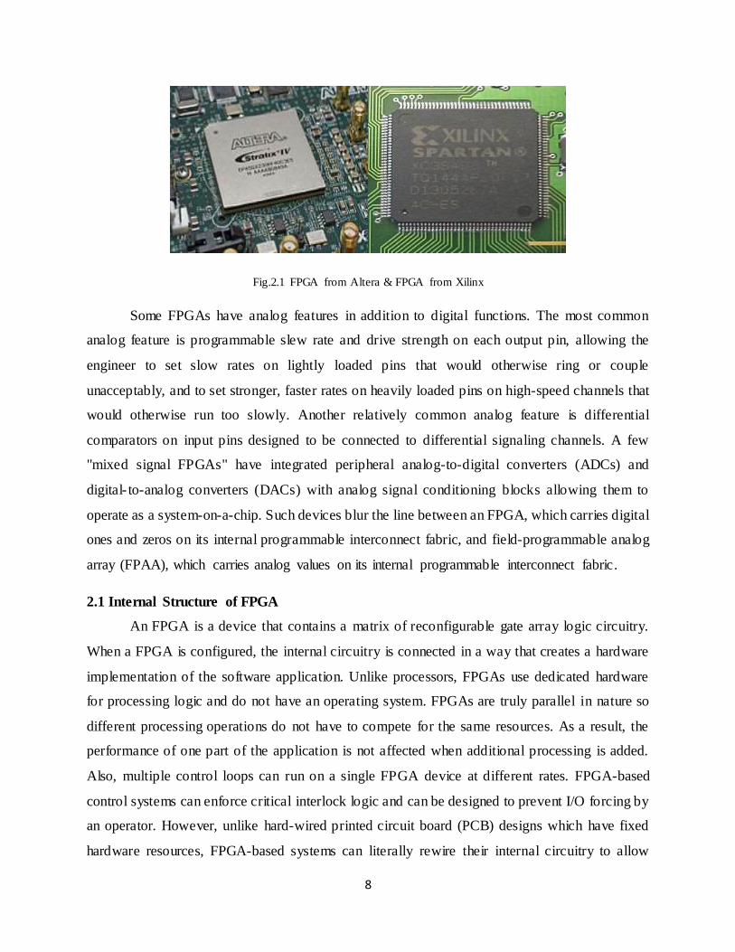
Fig.2.1 FPGA from Altera & FPGA from Xilinx
Some FPGAs have analog features in addition to digital functions. The most common
analog feature is programmable slew rate and drive strength on each output pin, allowing the
engineer to set slow rates on lightly loaded pins that would otherwise ring or couple
unacceptably, and to set stronger, faster rates on heavily loaded pins on high-speed channels that
would otherwise run too slowly. Another relatively common analog feature is differential
comparators on input pins designed to be connected to differential signaling channels. A few
"mixed signal FPGAs" have integrated peripheral analog-to-digital converters (ADCs) and
digital- to-analog converters (DACs) with analog signal conditioning blocks allowing them to
operate as a system-on-a-chip. Such devices blur the line between an FPGA, which carries digital
ones and zeros on its internal programmable interconnect fabric, and field-programmable analog
array (FPAA), which carries analog values on its internal programmable interconnect fabric.
2.1 Internal Structure of FPGA
An FPGA is a device that contains a matrix of reconfigurable gate array logic circuitry.
When a FPGA is configured, the internal circuitry is connected in a way that creates a hardware
implementation of the software application. Unlike processors, FPGAs use dedicated hardware
for processing logic and do not have an operating system. FPGAs are truly parallel in nature so
different processing operations do not have to compete for the same resources. As a result, the
performance of one part of the application is not affected when additional processing is added.
Also, multiple control loops can run on a single FPGA device at different rates. FPGA-based
control systems can enforce critical interlock logic and can be designed to prevent I/O forcing by
an operator. However, unlike hard-wired printed circuit board (PCB) designs which have fixed
hardware resources, FPGA-based systems can literally rewire their internal circuitry to allow
9
reconfiguration after the control system is deployed to the field. FPGA devices deliver the
performance and reliability of dedicated hardware circuitry.
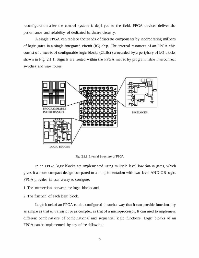
A single FPGA can replace thousands of discrete components by incorporating millions
of logic gates in a single integrated circuit (IC) chip. The internal resources of an FPGA chip
consist of a matrix of configurable logic blocks (CLBs) surrounded by a periphery of I/O blocks
shown in Fig. 2.1.1. Signals are routed within the FPGA matrix by programmable interconnect
switches and wire routes.
Fig. 2.1.1 Internal Structure of FPGA
In an FPGA logic blocks are implemented using multiple level low fan- in gates, which
gives it a more compact design compared to an implementation with two-level AND-OR logic.
FPGA provides its user a way to configure:
1. The intersection between the logic blocks and
2. The function of each logic block.
Logic blockof an FPGA can be configured in such a way that it can provide functionality
as simple as that of transistor or as complex as that of a microprocessor. It can used to implement
different combinations of combinational and sequential logic functions. Logic blocks of an
FPGA can be implemented by any of the following:
10
1. Transistor pairs
2. combinational gates like basic NAND gates or XOR gates
3. n-input Lookup tables
4. Multiplexers
5. Wide fan-in And-OR structure.
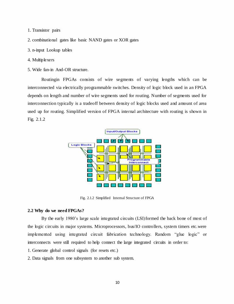
Routingin FPGAs consists of wire segments of varying lengths which can be
interconnected via electrically programmable switches. Density of logic block used in an FPGA
depends on length and number of wire segments used for routing. Number of segments used for
interconnection typically is a tradeoff between density of logic blocks used and amount of area
used up for routing. Simplified version of FPGA internal architecture with routing is shown in
Fig. 2.1.2
Fig. 2.1.2 Simplified Internal Structure of FPGA
2.2 Why do we need FPGAs?
By the early 1980’s large scale integrated circuits (LSI)formed the back bone of most of
the logic circuits in major systems. Microprocessors, bus/IO controllers, system timers etc.were
implemented using integrated circuit fabrication technology. Random “glue logic” or
interconnects were still required to help connect the large integrated circuits in order to:
1. Generate global control signals (for resets etc.)
2. Data signals from one subsystem to another sub system.
11
Systems typically consisted of few large scale integrated components and large number
of SSI (small scale integrated circuit) and MSI (medium scale integrated circuit)
components.Initial attempt to solve this problem led to development of Custom ICswhich were
to replace the large amount of interconnect. This reduced system complexity and manufacturing
cost, and improved performance. However, custom ICs have their own disadvantages. They are
relatively very expensive to develop, and delay introduced for product to market (time to market)
because of increased design time. There are two kinds of costs involved in development of
custom ICs
1. Cost of development and design
2. Cost of manufacture
(A trade off usually exists between the two costs)
Therefore the custom IC approach was only viable for products with very high volume,
and which were not time to market sensitive.FPGAs were introduced as an alternative to custom
ICs for implementing entire system on one chip and to provide flexibility of reprogramability to
the user. Introduction of FPGAs resulted in improvement of density relative to discrete SSI/MSI
components (within around 10x of custom ICs). Another advantage of FPGAs over Custom ICs
is that with the help of computer aided design (CAD) tools circuits could be implemented in a
short amount of time (no physical layout process, no mask making, no IC manufacturing).
2.3 Hardware design and development
The process of creating digital logic is not unlike the embedded software development
process. A description of the hardware's structure and behavior is written in a high- level
hardware description language (usually VHDL or Verilog) and that code is then compiled and
downloaded prior to execution. Of course, schematic capture is also an option for design entry,
but it has become less popular as designs have become more complex and the language-based
tools have improved. The overall process of hardware development for programmable logic is
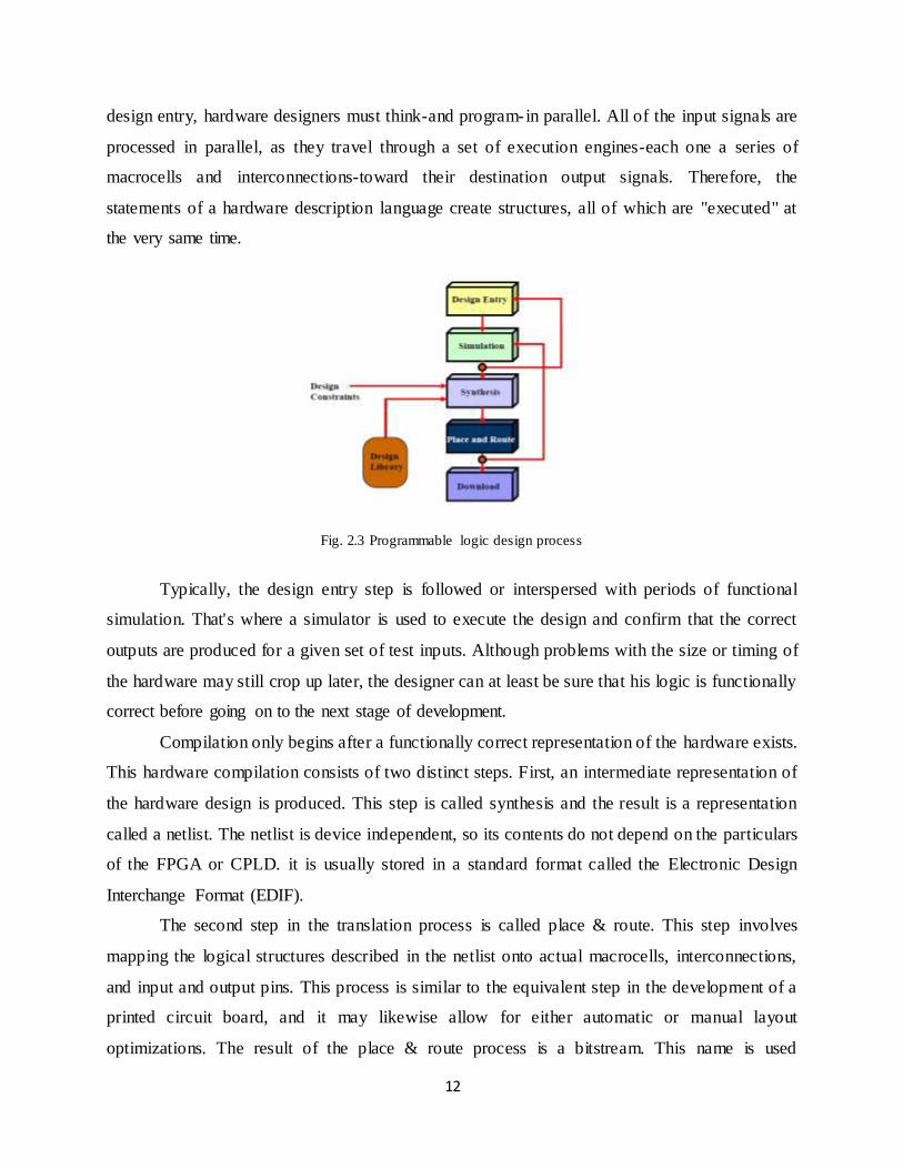
shown in Fig. 2.3 and described in the paragraphs that follow.
Perhaps the most striking difference between hardware and software design is the way a
developer must think about the problem. Software developers tend to think sequentially, even
when they are developing a multithreaded application. The lines of source code that they write
are always executed in that order, at least within a given thread. If there is an operating system it
is used to create the appearance of parallelism, but there is still just one execution engine. During
12
design entry, hardware designers must think-and program-in parallel. All of the input signals are
processed in parallel, as they travel through a set of execution engines-each one a series of
macrocells and interconnections-toward their destination output signals. Therefore, the
statements of a hardware description language create structures, all of which are "executed" at
the very same time.
Fig. 2.3 Programmable logic design process
Typically, the design entry step is followed or interspersed with periods of functional
simulation. That's where a simulator is used to execute the design and confirm that the correct
outputs are produced for a given set of test inputs. Although problems with the size or timing of
the hardware may still crop up later, the designer can at least be sure that his logic is functionally
correct before going on to the next stage of development.
Compilation only begins after a functionally correct representation of the hardware exists.
This hardware compilation consists of two distinct steps. First, an intermediate representation of
the hardware design is produced. This step is called synthesis and the result is a representation
called a netlist. The netlist is device independent, so its contents do not depend on the particulars
of the FPGA or CPLD. it is usually stored in a standard format called the Electronic Design
Interchange Format (EDIF).
The second step in the translation process is called place & route. This step involves
mapping the logical structures described in the netlist onto actual macrocells, interconnections,
and input and output pins. This process is similar to the equivalent step in the development of a
printed circuit board, and it may likewise allow for either automatic or manual layout
optimizations. The result of the place & route process is a bitstream. This name is used
13
generically, despite the fact that each CPLD or FPGA (or family) has its own, usually
proprietary, bitstream format. Suffice it to say that the bitstream is the binary data that must be
loaded into the FPGA or CPLD to cause that chip to execute a particular hardware design.
Increasingly there are also debuggers available that at least allow for single-stepping the
hardware design as it executes in the programmable logic device. But those only complement a
simulation environment that is able to use some of the information generated during the place &
route step to provide gate- level simulation. Obviously, this type of integration of device-specific
information into a generic simulator requires a good working relationship between the chip and
simulation tool vendors.
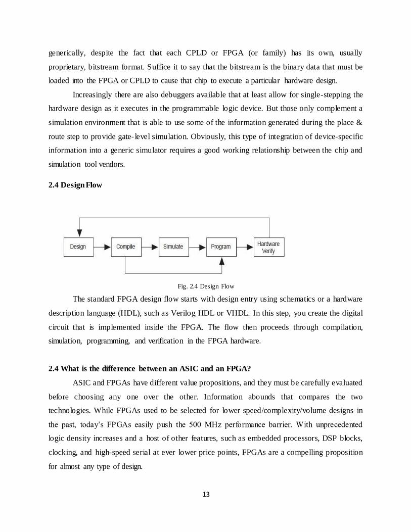
2.4 Design Flow
Fig. 2.4 Design Flow
The standard FPGA design flow starts with design entry using schematics or a hardware
description language (HDL), such as Verilog HDL or VHDL. In this step, you create the digital
circuit that is implemented inside the FPGA. The flow then proceeds through compilation,
simulation, programming, and verification in the FPGA hardware.
2.4 What is the difference between an ASIC and an FPGA?
ASIC and FPGAs have different value propositions, and they must be carefully evaluated
before choosing any one over the other. Information abounds that compares the two
technologies. While FPGAs used to be selected for lower speed/complexity/volume designs in
the past, today’s FPGAs easily push the 500 MHz performance barrier. With unprecedented
logic density increases and a host of other features, such as embedded processors, DSP blocks,
clocking, and high-speed serial at ever lower price points, FPGAs are a compelling proposition
for almost any type of design.
14
CHAPTER NO. 3
Pulse Width Modulation (PWM)
Pulse-width modulation (PWM), or pulse-duration modulation (PDM), is a modulation
technique that controls the width of the pulse, formally the pulse duration, based on modulator
signal information. Although this modulation technique can be used to encode information for
transmission, its main use is to allow the control of the power supplied to electrical devices,
especially to inertial loads such as motors.
The average value of voltage (and current) fed to the load is controlled by turning the
switch between supply and load on and off at a fast pace. The longer the switch is on compared
to the off periods, the higher the power supplied to the load.
The PWM switching frequency has to be much higher than what would affect the load
(the device that uses the power), which is to say that the resultant waveform perceived by the
load must be as smooth as possible. Typically switching has to be done several times a minute in
an electric stove, 120 Hz in a lamp dimmer, from few kilohertz (kHz) to tens of kHz for a motor
drive and well into the tens or hundreds of kHz in audio amplifiers and computer power supplies.
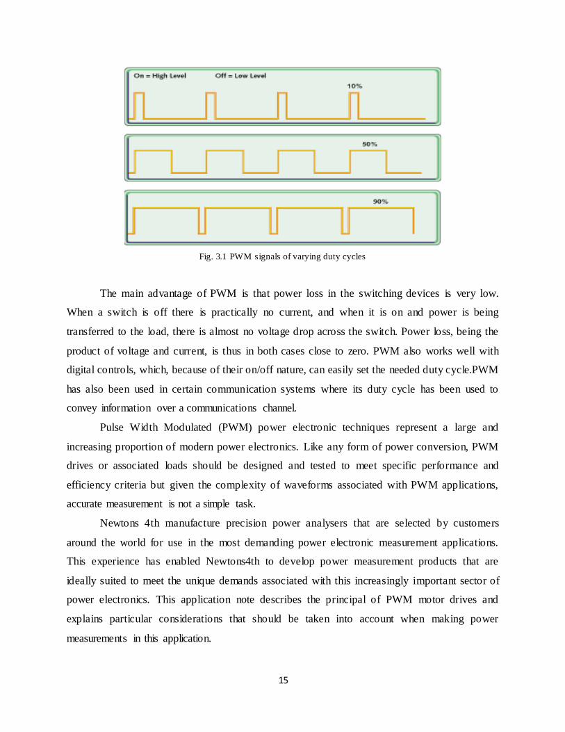
The term duty cycle describes the proportion of 'on' time to the regular interval or 'period' of
time, a low duty cycle corresponds to low power, because the power is off for most of the time.
Duty cycle is expressed in percent, 100% being fully on.
A PWM signal is not constant. Rather, the signal is on for part of its period, and off for
the rest. The dutycycle, D, refers to the percentage of the period for which the signal is o n. The
duty cycle can be anywherefrom 0, the signal is always off, to 1, where the signal is constantly
on. A 50% D results in a perfect squarewave.
15
Fig. 3.1 PWM signals of varying duty cycles
The main advantage of PWM is that power loss in the switching devices is very low.
When a switch is off there is practically no current, and when it is on and power is being
transferred to the load, there is almost no voltage drop across the switch. Power loss, being the
product of voltage and current, is thus in both cases close to zero. PWM also works well with
digital controls, which, because of their on/off nature, can easily set the needed duty cycle.PWM
has also been used in certain communication systems where its duty cycle has been used to
convey information over a communications channel.
Pulse Width Modulated (PWM) power electronic techniques represent a large and
increasing proportion of modern power electronics. Like any form of power conversion, PWM
drives or associated loads should be designed and tested to meet specific performance and
efficiency criteria but given the complexity of waveforms associated with PWM applications,
accurate measurement is not a simple task.
Newtons 4th manufacture precision power analysers that are selected by customers
around the world for use in the most demanding power electronic measurement applications.
This experience has enabled Newtons4th to develop power measurement products that are
ideally suited to meet the unique demands associated with this increasingly important sector of
power electronics. This application note describes the principal of PWM motor drives and
explains particular considerations that should be taken into account when making power
measurements in this application.
16
3.1 Why use PWM for speed variation?
When an AC motor is connected directly to an AC line (415V 3Φ for example) the motor
speed is fixed and is calculated as follows:
Ns =120𝑓
𝑝− 𝑆𝑙𝑖𝑝
Ns = Motor speed f = fundamental frequency(Hz) p = no. of poles
This is a problem since many applications need to change the speed of the motor, for
example changing the flow rate of a water pump by changing the speed of the propeller in a
pump. This was traditionally achieved by reducing the voltage across the windings of the motor,
which in turn reduced the current through the windings thus reducing motor torque. The speed of
the motor would reduce proportionally to voltage if the load on the motor remained the same but
this not an ideal solution since we know load is not always constant. Another reason this method
of control is not ideal is that when the slip on a motor is too great, the efficiency of the motor is
significantly reduced and if the load changes, so will motor speed. In light of this a more
sophisticated solution was required.
3.2 PWM Fundamentals
While PWM techniques can be applied to single or multi-phase applications, we will
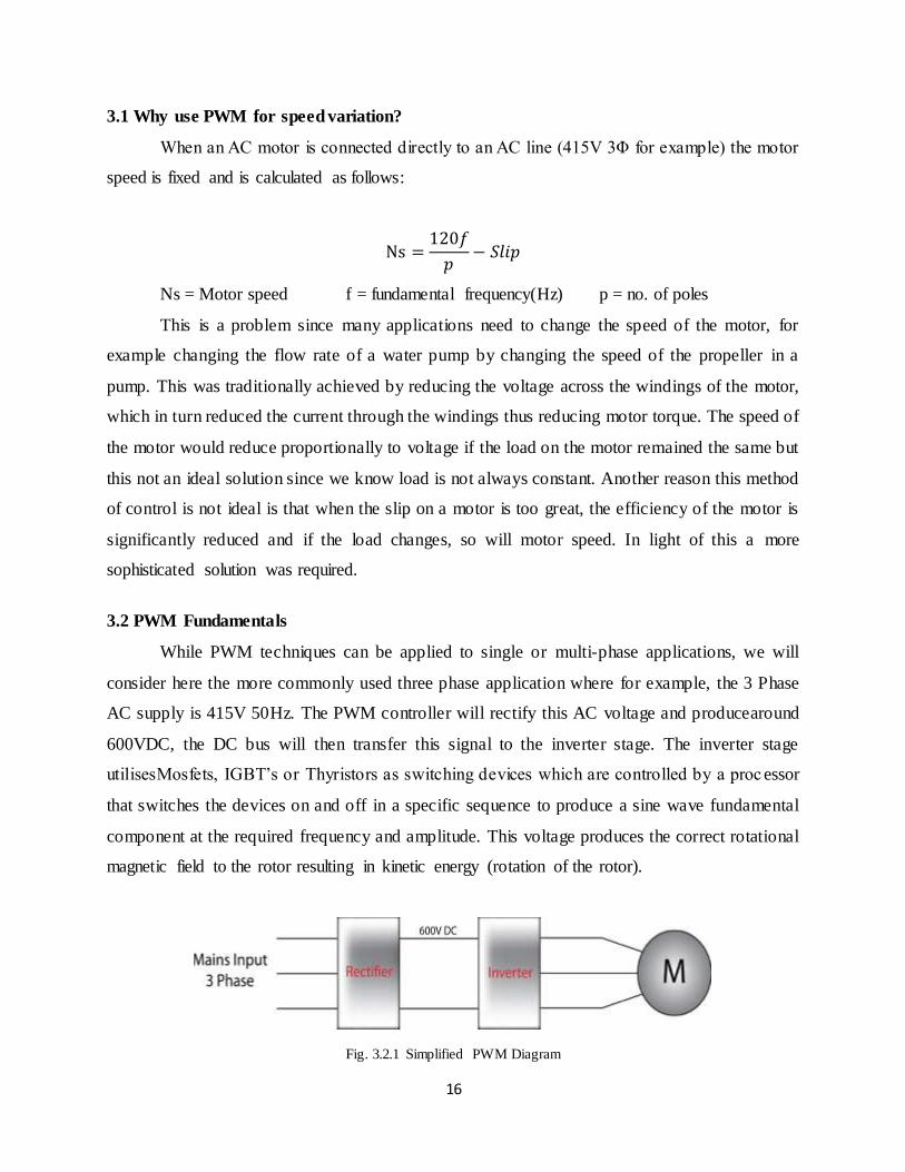
consider here the more commonly used three phase application where for example, the 3 Phase
AC supply is 415V 50Hz. The PWM controller will rectify this AC voltage and producearound
600VDC, the DC bus will then transfer this signal to the inverter stage. The inverter stage
utilisesMosfets, IGBT’s or Thyristors as switching devices which are controlled by a proc essor
that switches the devices on and off in a specific sequence to produce a sine wave fundamental
component at the required frequency and amplitude. This voltage produces the correct rotational
magnetic field to the rotor resulting in kinetic energy (rotation of the rotor).
Fig. 3.2.1 Simplified PWM Diagram
17
The above diagram represents the 3 Phase input, rectification, the DC interconnecting bus
and the Inverter stage, the output of which is transmitted to the motor and transferred into
mechanical power.
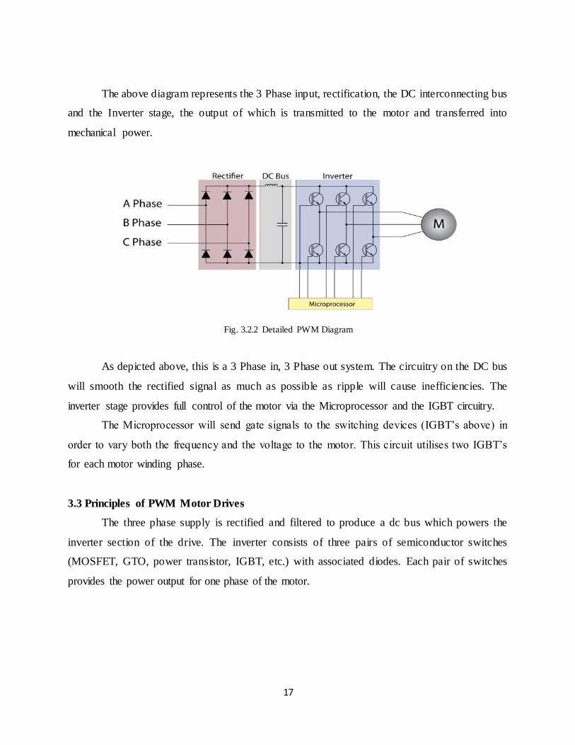
Fig. 3.2.2 Detailed PWM Diagram
As depicted above, this is a 3 Phase in, 3 Phase out system. The circuitry on the DC bus
will smooth the rectified signal as much as possible as ripple will cause inefficiencies. The
inverter stage provides full control of the motor via the Microprocessor and the IGBT circuitry.
The Microprocessor will send gate signals to the switching devices (IGBT’s above) in
order to vary both the frequency and the voltage to the motor. This circuit utilises two IGBT’s
for each motor winding phase.
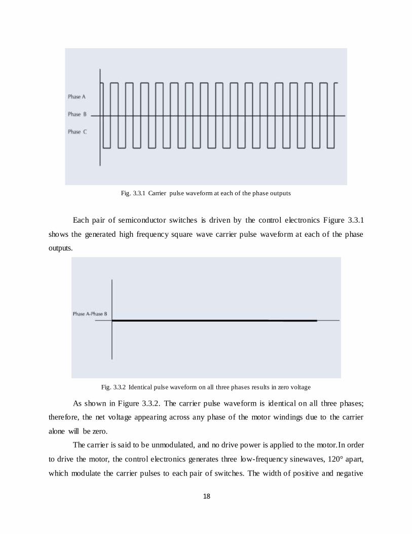
3.3 Principles of PWM Motor Drives
The three phase supply is rectified and filtered to produce a dc bus which powers the
inverter section of the drive. The inverter consists of three pairs of semiconductor switches
(MOSFET, GTO, power transistor, IGBT, etc.) with associated diodes. Each pair of switches
provides the power output for one phase of the motor.
18
Fig. 3.3.1 Carrier pulse waveform at each of the phase outputs
Each pair of semiconductor switches is driven by the control electronics Figure 3.3.1
shows the generated high frequency square wave carrier pulse waveform at each of the phase
outputs.
Fig. 3.3.2 Identical pulse waveform on all three phases results in zero voltage
As shown in Figure 3.3.2. The carrier pulse waveform is identical on all three phases;
therefore, the net voltage appearing across any phase of the motor windings due to the carrier
alone will be zero.
The carrier is said to be unmodulated, and no drive power is applied to the motor.In order
to drive the motor, the control electronics generates three low-frequency sinewaves, 120° apart,
which modulate the carrier pulses to each pair of switches. The width of positive and negative
19
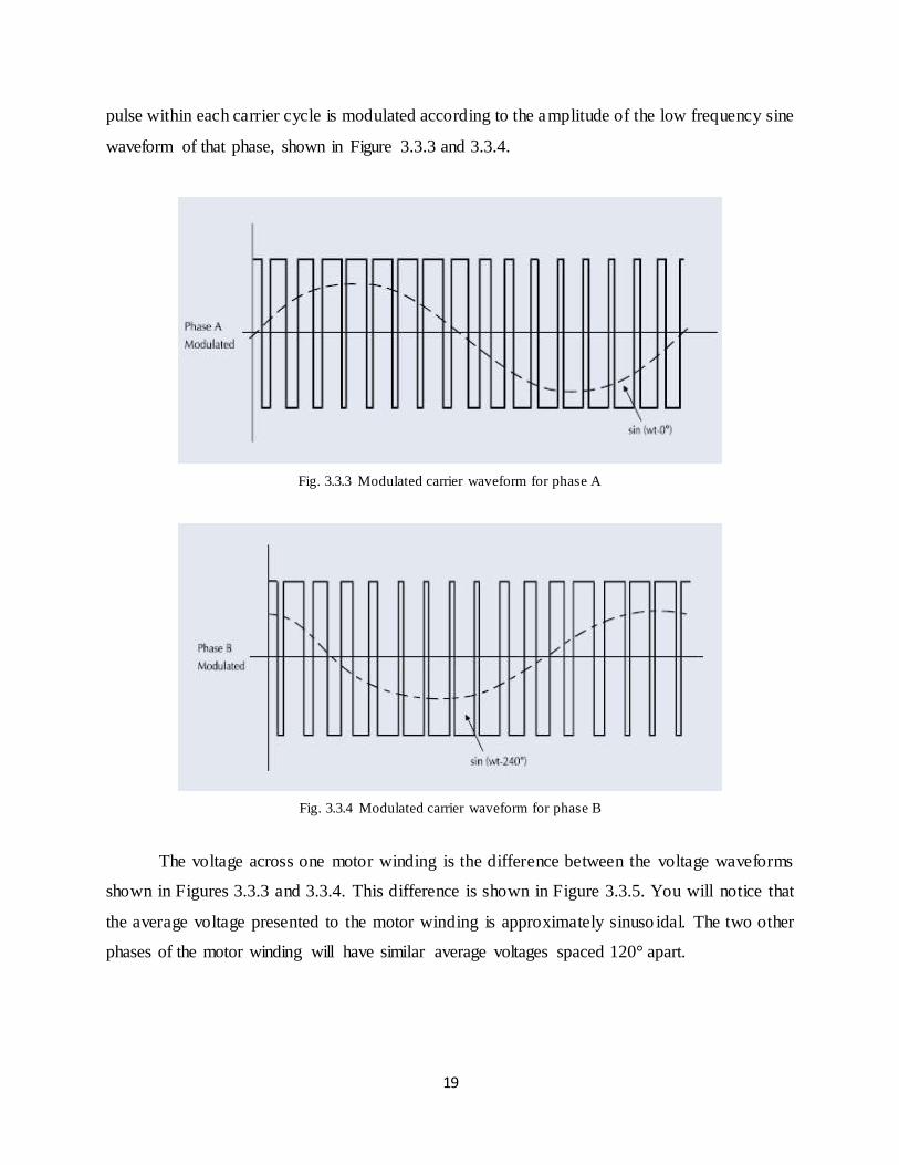
pulse within each carrier cycle is modulated according to the amplitude of the low frequency sine
waveform of that phase, shown in Figure 3.3.3 and 3.3.4.
Fig. 3.3.3 Modulated carrier waveform for phase A
Fig. 3.3.4 Modulated carrier waveform for phase B
The voltage across one motor winding is the difference between the voltage waveforms
shown in Figures 3.3.3 and 3.3.4. This difference is shown in Figure 3.3.5. You will notice that
the average voltage presented to the motor winding is approximately sinuso idal. The two other
phases of the motor winding will have similar average voltages spaced 120° apart.
20
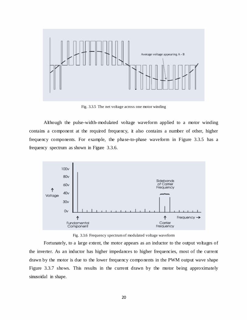
Fig. 3.3.5 The net voltage across one motor winding
Although the pulse-width-modulated voltage waveform applied to a motor winding
contains a component at the required frequency, it also contains a number of other, higher
frequency components. For example, the phase-to-phase waveform in Figure 3.3.5 has a
frequency spectrum as shown in Figure 3.3.6.
Fig. 3.3.6 Frequency spectrum of modulated voltage waveform
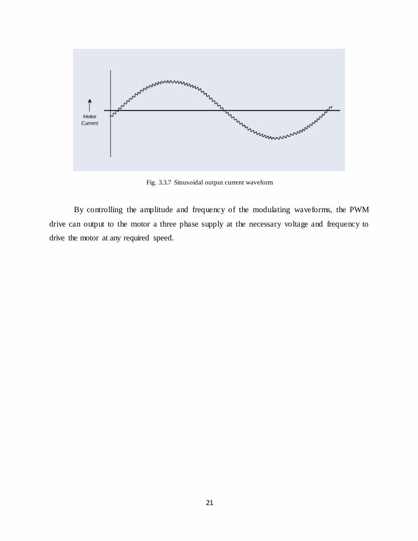
Fortunately, to a large extent, the motor appears as an inductor to the output voltages of
the inverter. As an inductor has higher impedances to higher frequencies, most of the current
drawn by the motor is due to the lower frequency components in the PWM output wave shape
Figure 3.3.7 shows. This results in the current drawn by the motor being approximately
sinusoidal in shape.
21
Fig. 3.3.7 Sinusoidal output current waveform
By controlling the amplitude and frequency of the modulating waveforms, the PWM
drive can output to the motor a three phase supply at the necessary voltage and frequency to
drive the motor at any required speed.
22
CHAPTER NO. 4
OPTOCOUPLER
In electronics, an opto- isolator, also called an optocoupler, photocoupler, or optical
isolator, is a component that transfers electrical signals between two isolated circuits by using
light. Opto- isolators prevent high voltages from affecting the system receiving the signal.
Commercially available opto- isolators withstand input-to-output voltages up to 10 Kvand voltage
transients with speeds up to 10 kV/μs.
A common type of opto- isolator consists of an LED and a phototransistor in the same
opaque package. Other types of source-sensor combinations include LED-photodiode, LED-
LASCR, and lamp-photoresistor pairs. Usually opto- isolators transfer digital (on-off) signals, but
some techniques allow them to be used with analog signals.
4.1 Operation
An opto- isolator contains a source (emitter) of light, almost always a near infrared light-
emitting diode (LED), that converts electrical input signal into light, a closed optical channel
(also called dielectrical channel), and a photosensor, which detects incoming light and either
generates electric energy directly, or modulates electric current flowing from an external power
supply. The sensor can be a photoresistor, a photodiode, a phototransistor, a silicon-controlled
rectifier (SCR) or a triac. Because LEDs can sense light in addition to emitting it, construction of
symmetrical, bi-directional opto-isolators is possible. An optocoupled solid state relay contains a
photodiode opto- isolator which drives a power switch, usually a complementary pair of
MOSFETs. A slotted optical switch contains a source of light and a sensor, but its optical
channel is open, allowing modulation of light by external objects obstructing the path of light or
reflecting light into the sensor.
4.2 Electric isolation
Electronic equipments and signal and power transmission lines can be subjected to
voltage surges induced by lightning, electrostatic discharge, radio frequency transmissions,
switching pulses (spikes) and perturbations in power supply. Remote lightning strikes can induce
surges up to 10 kV, one thousand times more than the voltage limits of many electronic
23
components. A circuit can also incorporate high voltages by design, in which case it needs safe,
reliable means of interfacing its high-voltage components with low-voltage ones.
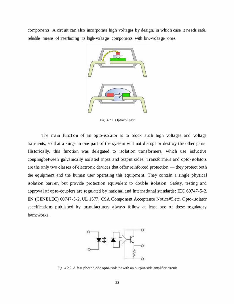
Fig. 4.2.1 Optocoupler
The main function of an opto-isolator is to block such high voltages and voltage
transients, so that a surge in one part of the system will not disrupt or destroy the other parts.
Historically, this function was delegated to isolation transformers, which use inductive
couplingbetween galvanically isolated input and output sides. Transformers and opto- isolators
are the only two classes of electronic devices that offer reinforced protection — they protect both
the equipment and the human user operating this equipment. They contain a single physical
isolation barrier, but provide protection equivalent to double isolation. Safety, testing and
approval of opto-couplers are regulated by national and international standards: IEC 60747-5-2,
EN (CENELEC) 60747-5-2, UL 1577, CSA Component Acceptance Notice#5,etc. Opto- isolator
specifications published by manufacturers always follow at least one of these regulatory
frameworks.
Fig. 4.2.2 A fast photodiode opto-isolator with an output-side amplifier circuit
24
An opto- isolator connects input and output sides with a beam of light modulated by input
current. It transforms useful input signal into light, sends it across the dielectric channel, captures
light on the output side and transforms it back into electric signal. Unlike transformers, which
pass energy in both directions with very low losses, opto- isolators are unidirectional and they
cannot transmit power. Typical opto- isolators can only modulate the flow of energy already
present on the output side. Unlike transformers, opto- isolators can pass DC or slow-moving
signals and do not require matching impedances between input and output sides. Both
transformers and opto- isolators are effective in breaking ground loops, common in industrial and
stage equipment, caused by high or noisy return currents in ground wires.
The physical layout of an opto- isolator depends primarily on the desired isolation
voltage. Devices rated for less than a few kV have planar (or sandwich) construction. The sensor
die is mounted directly on the lead frame of its package (usually, a six-pin or a four-pin dual in-
line package). The sensor is covered with a sheet of glass or clear plastic, which is topped with
the LED die. The LED beam fires downward. To minimize losses of light, the useful absorption
spectrum of the sensor must match the output spectrum of the LED, which almost invariably lies
in the near infrared.The optical channel is made as thin as possible for a desired breakdown
voltage. For example, to be rated for short-term voltages of 3.75 kV and transients of 1 kV/μs,
the clear polyimide sheet in the Avago ASSR-300 series is only 0.08 mm thick. Breakdown
voltages of planar assemblies depend on the thickness of the transparent sheet and the
configuration of bonding wires that connect the dies with external pins. Real in-circuit isolation
voltage is further reduced by creepage over the PCB and the surface of the package. Safe design
rules require a minimal clearance of 25 mm/kV for bare metal conductors or 8.3 mm/kV for
coated conductors.
Opto-isolators rated for 2.5 to 6 kV employ a different layout called silicone dome. Here,
the LED and sensor dies are placed on the opposite sides of the package; the LED fires into the
sensor horizontally. The LED, the sensor and the gap between them are encapsulated in a blob,
or dome, of transparent silicone. The dome acts as a reflector, retaining all stray light and
reflecting it onto the surface of the sensor, minimizing losses in a relatively long optical channel.
In double mold designs the space between the silicone blob ("inner mold") and the outer shell
("outer mold") is filled with dark dielectric compound with a matched coefficient of thermal
expansion.
25
CHAPTER NO. 5
CONCLUSION
The FPGA controller is used for PWM adjustable speed control of AC motors. The speed
control of Induction motor is achieved by controlling modulation of pulse width with the help of
FPGA controller. By controlling the amplitude and frequency of the modulating waveforms, the
PWM drive can output to the motor a three phase supply at the necessary voltage and frequency
to drive the motor at any required speed.The use of an efficient and lower cost controller based
on FPGA programming to control the speed of motor. Due to the simplistic nature of this control,
it has the potential to be implemented in a low cost application.
26
REFERENCES
1. Anthony Cataldo, “Low-priced FPGA options set to expand” Electronic Engineering Times
Journal, N 1361, PP 38-45, USA 2005.
2. www.tektronix.com/power-analyzer/power analysis of pwm motor drives
application note
3. D. Deng, S. Chen,G. Joos, “FPGA implementation of PWM pattern generators”,Canadian
Conference on Electrical and Computer Engineering, V1, PP 225-230 May2001. and Electronics
Engineers Inc.
4. R. M. Pindoriya, S. Rajendran, P. J. Chauhan “Speed Control of BLDC Motor using
Sinusoidal PWM Technique”,National Conference On Emerging Trends In Computer &
Electrical Engineering ETCEE-2014, Page 151-156
5. http://en.wikipedia.org/wiki/Duty_cycle.
6. Eric Monmasson, Lahoucine Idkhajine, Marcian N. Cirstea, ImeneBahri, AlinTisan, and
Mohamed Wissem Naouar “FPGAs in Industrial Control Applicalication IEEE Transactions On
Industrial Informatics, Vol. 7, No. 2, May 2011
Related Documents