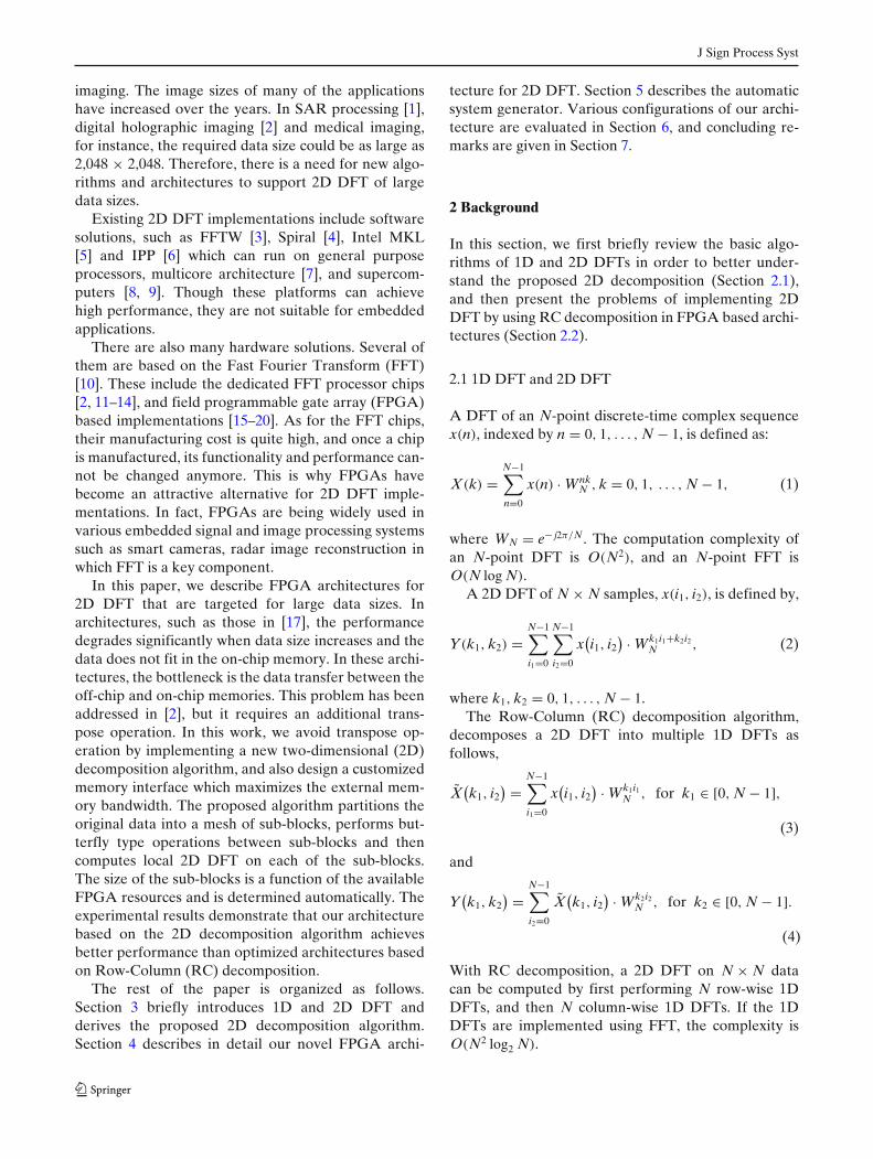
J Sign Process Syst DOI 10.1007/s11265-010-0500-y FPGA Architecture for 2D Discrete Fourier Transform Based on 2D Decomposition for Large-sized Data Chi-Li Yu · Jung-Sub Kim · Lanping Deng · Srinidhi Kestur · Vijaykrishnan Narayanan · Chaitali Chakrabarti Received: 14 January 2010 / Revised: 25 May 2010 / Accepted: 26 May 2010 © Springer Science+Business Media, LLC 2010 Abstract Applications based on Discrete Fourier Transforms (DFT) are extensively used in several areas of signal and digital image processing. Of particular interest is the two-dimensional (2D) DFT which is more computation- and bandwidth-intensive than the one-dimensional (1D) DFT. Traditionally, a 2D DFT is computed using Row-Column (RC) decomposition, where 1D DFTs are computed along the rows fol- lowed by 1D DFTs along the columns. Both application This paper is an extension of our paper that appeared in SIPS ’09. The added sections are: (1) Impact of large data size on conventional 2D DFT architecture (Section 2.2); (2) Detailed descriptions of the infrastructure components of the FPGA platform (Section 4.2); (3) Detailed description of the automatic 2D DFT system generator (Section 5); (4) Accuracy analysis of the 2D DFT (Section 6.4). C.-L. Yu (B ) · L. Deng · C. Chakrabarti School of Electrical, Computer and Energy Engineering, Arizona State University, Tempe, AZ, USA e-mail: [email protected] L. Deng e-mail: [email protected] C. Chakrabarti e-mail: [email protected] J.-S. Kim · S. Kestur · V. Narayanan Department of Computer Science and Engineering, Pennsylvania State University, University Park, PA, USA J.-S. Kim e-mail: [email protected] S. Kestur e-mail: [email protected] V. Narayanan e-mail: [email protected] specific and reconfigurable hardware have utilized this scheme for high-performance implementations of 2D DFT. However, architectures based on RC decompo- sition are not efficient for large input size data due to memory bandwidth constraints. In this paper, we propose an efficient architecture to implement 2D DFT for large-sized input data based on a novel 2D de- composition algorithm. This architecture achieves very high throughput by exploiting the inherent parallelism due to the algorithm decomposition and by utilizing the row-wise burst access pattern of the external mem- ory. A high throughput memory interface has been designed to enable maximum utilization of the memory bandwidth. In addition, an automatic system gener- ator is provided for mapping this architecture onto a reconfigurable platform of Xilinx Virtex-5 devices. For a 2 K × 2 K input size, the proposed architecture is 1.96 times faster than RC decomposition based im- plementation under the same memory constraints, and also outperforms other existing implementations. Keywords Multi-dimensional signal processing · DFT · Algorithm-architecture co-design 1 Introduction Discrete Fourier Transform (DFT) is widely used in digital signal processing (DSP) and scientific computing applications. In particular, the two-dimensional (2D) DFT is used in a wide variety of imaging applications which need spectral and frequency-domain analysis such as, image watermarking, finger print recognition, synthetic aperture radar (SAR) processing and medical

Welcome message from author
This document is posted to help you gain knowledge. Please leave a comment to let me know what you think about it! Share it to your friends and learn new things together.
Transcript
J Sign Process SystDOI 10.1007/s11265-010-0500-y
FPGA Architecture for 2D Discrete Fourier TransformBased on 2D Decomposition for Large-sized Data
Chi-Li Yu · Jung-Sub Kim · Lanping Deng ·Srinidhi Kestur · Vijaykrishnan Narayanan ·Chaitali Chakrabarti
Received: 14 January 2010 / Revised: 25 May 2010 / Accepted: 26 May 2010© Springer Science+Business Media, LLC 2010
Abstract Applications based on Discrete FourierTransforms (DFT) are extensively used in several areasof signal and digital image processing. Of particularinterest is the two-dimensional (2D) DFT which ismore computation- and bandwidth-intensive than theone-dimensional (1D) DFT. Traditionally, a 2D DFTis computed using Row-Column (RC) decomposition,where 1D DFTs are computed along the rows fol-lowed by 1D DFTs along the columns. Both application
This paper is an extension of our paper that appeared inSIPS ’09. The added sections are: (1) Impact of large datasize on conventional 2D DFT architecture (Section 2.2);(2) Detailed descriptions of the infrastructure componentsof the FPGA platform (Section 4.2); (3) Detailed descriptionof the automatic 2D DFT system generator (Section 5);(4) Accuracy analysis of the 2D DFT (Section 6.4).
C.-L. Yu (B) · L. Deng · C. ChakrabartiSchool of Electrical, Computer and Energy Engineering,Arizona State University, Tempe, AZ, USAe-mail: [email protected]
L. Denge-mail: [email protected]
C. Chakrabartie-mail: [email protected]
J.-S. Kim · S. Kestur · V. NarayananDepartment of Computer Science and Engineering,Pennsylvania State University, University Park, PA, USA
J.-S. Kime-mail: [email protected]
S. Kesture-mail: [email protected]
V. Narayanane-mail: [email protected]
specific and reconfigurable hardware have utilized thisscheme for high-performance implementations of 2DDFT. However, architectures based on RC decompo-sition are not efficient for large input size data dueto memory bandwidth constraints. In this paper, wepropose an efficient architecture to implement 2D DFTfor large-sized input data based on a novel 2D de-composition algorithm. This architecture achieves veryhigh throughput by exploiting the inherent parallelismdue to the algorithm decomposition and by utilizingthe row-wise burst access pattern of the external mem-ory. A high throughput memory interface has beendesigned to enable maximum utilization of the memorybandwidth. In addition, an automatic system gener-ator is provided for mapping this architecture ontoa reconfigurable platform of Xilinx Virtex-5 devices.For a 2K × 2K input size, the proposed architectureis 1.96 times faster than RC decomposition based im-plementation under the same memory constraints, andalso outperforms other existing implementations.
Keywords Multi-dimensional signal processing ·DFT · Algorithm-architecture co-design
1 Introduction
Discrete Fourier Transform (DFT) is widely used indigital signal processing (DSP) and scientific computingapplications. In particular, the two-dimensional (2D)DFT is used in a wide variety of imaging applicationswhich need spectral and frequency-domain analysissuch as, image watermarking, finger print recognition,synthetic aperture radar (SAR) processing and medical
J Sign Process Syst
imaging. The image sizes of many of the applicationshave increased over the years. In SAR processing [1],digital holographic imaging [2] and medical imaging,for instance, the required data size could be as large as2,048 × 2,048. Therefore, there is a need for new algo-rithms and architectures to support 2D DFT of largedata sizes.
Existing 2D DFT implementations include softwaresolutions, such as FFTW [3], Spiral [4], Intel MKL[5] and IPP [6] which can run on general purposeprocessors, multicore architecture [7], and supercom-puters [8, 9]. Though these platforms can achievehigh performance, they are not suitable for embeddedapplications.
There are also many hardware solutions. Several ofthem are based on the Fast Fourier Transform (FFT)[10]. These include the dedicated FFT processor chips[2, 11–14], and field programmable gate array (FPGA)based implementations [15–20]. As for the FFT chips,their manufacturing cost is quite high, and once a chipis manufactured, its functionality and performance can-not be changed anymore. This is why FPGAs havebecome an attractive alternative for 2D DFT imple-mentations. In fact, FPGAs are being widely used invarious embedded signal and image processing systemssuch as smart cameras, radar image reconstruction inwhich FFT is a key component.
In this paper, we describe FPGA architectures for2D DFT that are targeted for large data sizes. Inarchitectures, such as those in [17], the performancedegrades significantly when data size increases and thedata does not fit in the on-chip memory. In these archi-tectures, the bottleneck is the data transfer between theoff-chip and on-chip memories. This problem has beenaddressed in [2], but it requires an additional trans-pose operation. In this work, we avoid transpose op-eration by implementing a new two-dimensional (2D)decomposition algorithm, and also design a customizedmemory interface which maximizes the external mem-ory bandwidth. The proposed algorithm partitions theoriginal data into a mesh of sub-blocks, performs but-terfly type operations between sub-blocks and thencomputes local 2D DFT on each of the sub-blocks.The size of the sub-blocks is a function of the availableFPGA resources and is determined automatically. Theexperimental results demonstrate that our architecturebased on the 2D decomposition algorithm achievesbetter performance than optimized architectures basedon Row-Column (RC) decomposition.
The rest of the paper is organized as follows.Section 3 briefly introduces 1D and 2D DFT andderives the proposed 2D decomposition algorithm.Section 4 describes in detail our novel FPGA archi-
tecture for 2D DFT. Section 5 describes the automaticsystem generator. Various configurations of our archi-tecture are evaluated in Section 6, and concluding re-marks are given in Section 7.
2 Background
In this section, we first briefly review the basic algo-rithms of 1D and 2D DFTs in order to better under-stand the proposed 2D decomposition (Section 2.1),and then present the problems of implementing 2DDFT by using RC decomposition in FPGA based archi-tectures (Section 2.2).
2.1 1D DFT and 2D DFT
A DFT of an N-point discrete-time complex sequencex(n), indexed by n = 0, 1, . . . , N − 1, is defined as:
X(k) =N−1∑
n=0
x(n) · WnkN , k = 0, 1, . . . , N − 1, (1)
where WN = e− j2π/N . The computation complexity ofan N-point DFT is O(N2), and an N-point FFT isO(N log N).
A 2D DFT of N × N samples, x(i1, i2), is defined by,
Y(k1, k2) =N−1∑
i1=0
N−1∑
i2=0
x(i1, i2
) · Wk1i1+k2i2N , (2)
where k1, k2 = 0, 1, . . . , N − 1.The Row-Column (RC) decomposition algorithm,
decomposes a 2D DFT into multiple 1D DFTs asfollows,
X(k1, i2
) =N−1∑
i1=0
x(i1, i2
) · Wk1i1N , for k1 ∈ [0, N − 1],
(3)
and
Y(k1, k2
) =N−1∑
i2=0
X(k1, i2
) · Wk2i2N , for k2 ∈ [0, N − 1].
(4)
With RC decomposition, a 2D DFT on N × N datacan be computed by first performing N row-wise 1DDFTs, and then N column-wise 1D DFTs. If the 1DDFTs are implemented using FFT, the complexity isO(N2 log2 N).

J Sign Process Syst
FPGA
LocalMemory
ProcessingBlock
SRAM
Fig. 1 Basic 2D DFT architecture utilizing external memory.
2.2 Impact of Large Data Size on Conventional2D DFT Architectures
In an FPGA implementation of RC decompositionbased 2D DFT, the input 2D data is initially storedin the external memory, and row-wise DFTs followedby column-wise DFTs are performed. The basic archi-tecture utilizing Synchronous Random Access Memory(SRAM) based external memory is shown in Fig. 1.For row-DFTs/column-DFTs, fixed number of rows/columns of input data are loaded into FPGA localmemory, as shown in Fig. 2, and several 1D DFT coresare operated in parallel. This operation is repeateduntil all the rows/columns are traversed. This kind ofimplementation performs very well for small data sizes,since the row and column access times are same forSRAM.
For large data sizes, however, the SRAM solution be-comes impractical due to the limited size and high cost.In this case, Synchronous Dynamic RAM (SDRAM),which has much larger capacity, should be used as
Row-wise DFT Local Memory
Step 1 Step 2
Step nExternal Memory
(a) Row DFT
Column-wise DFT Local Memory
Step 1 Step 2
Step nExternal Memory
(b) Column DFT
Fig. 2 Data access pattern from external memory for row-DFTand column-DFT.
external memory. Because of its high throughput andhigh capacity, SDRAM is a standard component onmost FPGA boards.
SDRAM has a three-dimensional organization, com-posed of banks, rows, and columns. It has non-uniformaccess time; accessing consecutive elements in a row hasa low latency, while accessing data across different rowshas a high latency. So if RC decomposition is used, row-wise DFTs are much faster than column-wise DFTs,since SDRAM memory organization favors data accessalong rows. Thus, column-wise data access is a majorbottleneck for 2D DFT implementations.
Moreover, though the DDR2 and recent DDR3standards for SDRAMs can achieve higher data ratesfor reads and writes to external memory, existing mem-ory interface designs fail to utilize the bandwidth of theSDRAM device for column-DFTs. Even with a custommemory interface design, for large data sizes, conven-tional 2D DFT implementation with RC decompositionresults in poor performance.
An alternative and a popular approach to overcomethe imbalance of row-wise and column-wise memoryaccesses is to employ a transpose operation on the dataas an intermediate step in 2D DFT [2]. However, it re-quires data to be transferred to and from memory threetimes, which is cumbersome and inefficient for largedata sizes.
In the next section, we propose a new 2D decom-position algorithm which does not need the transposeoperation to mitigate the data access problem of RCdecomposition based algorithms, and can be efficientlymapped onto FPGA based architectures.
3 Decomposition Algorithms for DFT
In this section, the decomposition of 1D DFT is de-scribed in Section 3.1, followed by the 2D decompo-sition algorithm for 2D DFT in Section 3.2 and thefunctional components of the 2D DFT in Section 3.3.
3.1 Decomposition of 1D DFT
A 1D DFT of length N can be decomposed and com-puted by a series of smaller transforms and permu-tations. We first represent DFT in the matrix-vectormultiplication form as
[X0 X1 . . . XN−1
]T = FN · [x0 x1 . . . xN−1
]T, (5)
where FN is the twiddle factor matrix.
J Sign Process Syst
The decomposition of 1D DFT is essentially repre-sentation of FN as a product of sparse matrices and isdescribed as follows [21–23].
FN = PN,p(Ip ⊗ Fm
)DN
(Fp ⊗ Im
), (6)
where N = p · m, where p and m are both integers. Im
is an m × m identity matrix, DN is a diagonal matrixof twiddle factors, and ⊗ is the Kronecker or tensorproduct and can be expressed as
DN( j, j ) = W( j mod m)·� j/m�N for j = 0, 1 . . . N − 1, (7)
An ⊗ Bm = [ak,l Bm
]0≤k,l<n for An = [
ak,l]
0≤k,l<n. (8)
Finally, PN,p denotes permutation with stride p.The traditional radix-2 FFT can be considered a
specific case of recursive decomposition with factorp = 2.
3.2 2D Decomposition Algorithm
The general form of 2D DFT is described in matrixform as follows:
Y = FM · X · FTN = FM · X · FN, (9)
where input X and output Y are of size M × N; FM andFN are DFT matrices which are symmetric.
The expression (FM · X) is traditionally calculatedby applying an M-point DFT for each column of X.
As described in Section 3.1, an M-point DFT can bereplaced by the sparse matrix product form as depictedin Eq. 6. Hence, by partitioning a column of size M intop sub-blocks, the expression (FM · X) can be writtenas follows:
FM · X = PM,p · (Ip ⊗ FM/p)DM
(Fp ⊗ IM/p
) · X, (10)
where the permutation PM,p term in Eq. 6 is taken intoaccount in the final stage.
Similarly, the expression (X · FN) in Eq. 9 can bewritten as follows:
X · FN = X · (Fq ⊗ IN/q)DN
(Iq ⊗ FN/q
) · PN,q. (11)
Extending such a partitioning to both row-wise andcolumn-wise elements, the 2D decomposition of Eq. 9on a p × q mesh is written as follows:
Y = (Ip ⊗ FM/p
)DM
(Fp ⊗ IM/p
) · X
· (Fq ⊗ IN/q)DN
(Iq ⊗ FN/q
). (12)
Y is obtained by applying a bit-reverse permutation (P)on Y of Eq. 12.
3.3 Functional Components of the 2DDecomposition Algorithm
Equation 13 pictorially demonstrates the sequence ofoperations involved in the computation of the decom-posed 2D-DFT.
Y = P
⎛
⎜⎜⎜⎜⎜⎜⎜⎜⎜⎜⎜⎜⎝
(Ip ⊗ FM/p
)DM
(Fp ⊗ IM/p
) · X · (Fq ⊗ IN/q
)DN︸ ︷︷ ︸
Step 1︸ ︷︷ ︸Step 2
(Iq ⊗ FN/q
)
︸ ︷︷ ︸Step 3
⎞
⎟⎟⎟⎟⎟⎟⎟⎟⎟⎟⎟⎟⎠
. (13)
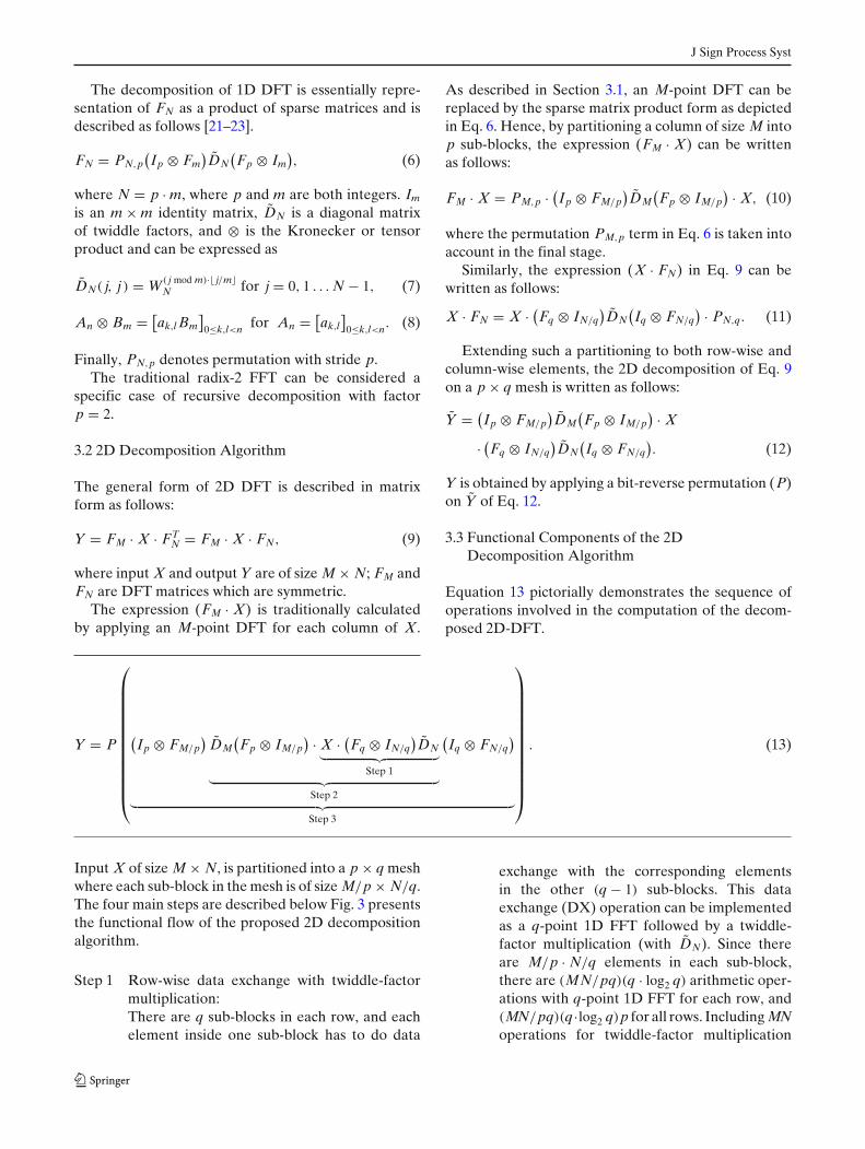
Input X of size M × N, is partitioned into a p × q meshwhere each sub-block in the mesh is of size M/p × N/q.The four main steps are described below Fig. 3 presentsthe functional flow of the proposed 2D decompositionalgorithm.
Step 1 Row-wise data exchange with twiddle-factormultiplication:There are q sub-blocks in each row, and eachelement inside one sub-block has to do data
exchange with the corresponding elementsin the other (q − 1) sub-blocks. This dataexchange (DX) operation can be implementedas a q-point 1D FFT followed by a twiddle-factor multiplication (with DN). Since thereare M/p · N/q elements in each sub-block,there are (MN/pq)(q · log2 q) arithmetic oper-ations with q-point 1D FFT for each row, and(MN/pq)(q·log2 q)p for all rows. Including MNoperations for twiddle-factor multiplication
J Sign Process Syst
Data Exchange- Row-wise
Twiddle-factorMultiplication
Data Exchange- Column-wise
Twiddle-factorMultiplication
Local2D-DFT
Permutation
Data exchange stage
Fig. 3 The functional flow graph of 2D DFT.
(DN), it takes a total of (MN/pq)(q·log2 q)p+MN ≈ O[MN(1+log2 q)] arithmetic operations.Note that all q-point 1D FFTs can be com-puted in parallel.
Step 2 Column-wise data exchange with twiddle-factor multiplication:
Y2 = DM(Fp ⊗ IM/p
) · Y1
Similar to Step 1, the DX is repeated for thep sub-blocks in each column. This step has acomplexity of O[MN(1 + log2 p)] operations.
INPUT:
Input size: N × N
Local 2D DFT size: K × K
Mesh size: (N / K ) × (N / K )
Local memory size: S × S
1. Data Exchange (DX)
for i = 1 : (N / S) × (N / S)
Load DX data into local memory
for j = 1 : 2(S/(N / K ))
Compute (N / K )-point 1D FFT with twiddle-factor
multiplication
Store the result back to external memory
2. Local 2D DFT (LDFT)
for i = 1 : (N / S) × (N / S)
Load LDFT data into local memory
for j = 1 : 2(S/ K )
Compute K -point 1D FFT
Store the result back to external memory
Fig. 4 Pseudo code for 2D decomposition algorithm for 2D DFT.
Step 3 Local 2D DFT on each sub-block:
Y = (Ip ⊗ FM/p
)Y2
(Iq ⊗ FN/q
)
After the row-wise and column-wise data ex-change with twiddle-factor multiplications, 2DDFT computation is performed on each sub-block of size M/p · N/q. This operation is fullyparallel for all sub-blocks, and only limited byresource constraints in the underlying archi-tecture. No data communication is requiredbetween any sub-blocks.
Step 4 Output permutation:
Y = P(Y)
A bit-reverse permutation is required beforegenerating the output. This is done by the hostcomputer before display.
The pseudo code of the 2D decomposition algorithmfor the case when the image is of size N × N is pre-sented in Fig. 4. The sub-blocks are of size K × K, themesh is of size (N/K) × (N/K), and the local memoryis of size S × S. Note that 1D DFT is computed alongrows and columns in each stage. Also notice that thereare other 2D decomposition methods, such as Vec-tor Radix FFT [24], which recursively decomposes the2D DFT into small-sized ones, like 2 × 2 or 4 × 4 2DDFT. While such methods can effectively reduce thenumber of multiplications, the recursive decompositionmakes hardware implementation and memory address-ing much more complicated.
4 Proposed 2D-DFT Architecture
Figure 5 gives a bird’s eye view of the FPGA architec-ture for implementing the 2D decomposition based 2DDFT. It is composed of several components that canbe classified broadly into Domain-specif ic componentsand Infrastructure components. Components such asprocessing elements (PEs) are designed specially forthe 2D DFT application and hence are domain-specific.Infrastructure components, including PowerPC, mem-ory interface, host connection and UART, provide

J Sign Process Syst
SDRAM
FPGA
Hig
h T
hrou
ghpu
tM
emor
y In
terf
ace
ProcessingElements
PowerPC
Hos
tC
onne
ctio
n
UART
Fig. 5 Block diagram of the FPGA architecture for 2D decom-position based 2D DFT.
high-level control and support for the domain-specificcomponents.
4.1 Domain-specific Components
As shown in Fig. 6, the PE array consists of multiplePEs, where each PE is formed by a primitive 1D FFTIP core and a complex multiplier. The primitive FFTis used for both data exchange and local 2D DFT. Inour design, we adopt Xilinx pipelined FFT IP [25]. Thecomplex multiplier is used for twiddle-factor multiplica-tion during data exchange. All PEs operate in paralleland access data from/to multi-banked local memory si-multaneously without conflicts. The number of PEs andsize of the primitive FFTs is determined by the memorybandwidth and available FPGA resources as explainedin Section 5. Note that for ease of implementation, aninput size of N × N is always assumed, where N is apower of 2, otherwise zero-padding is applied.
The input data is stored in the external memory(SDRAM), and is logically partitioned into a mesh ofsub-blocks. During each step mentioned in Section 3,portions of data are loaded into the FPGA local mem-ory, processed, and then stored back to the external
memory. There are two identical local memories thatserve as ping pong buffers. These local memories areimplemented with dual-port Block RAM (BRAM) onthe FPGA. The operations are described in detailsbelow.
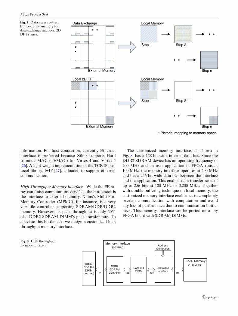
In the data exchange stage which consists of the firstfour blocks in Fig. 3, first, equal number of samplesfrom the same position in each sub-block is loaded intolocal memory. This data is then used for computingboth row-wise and column-wise data exchanges. Notethat the data from the external memory is accessedonly along the row direction as depicted in Fig. 7.This pattern is especially advantageous for accessing adynamic memory, such as DDR2 and DDR3 SDRAM,which only favors row-wise burst access. The operationsare repeated until the entire data is traversed, as shownin Fig. 7.
In the local 2D DFT stage (corresponding to the fifthblock in Fig. 3), fixed number of contiguous sub-blocksof the 2D data are loaded into FPGA local memory andthe PE array computes 1D transforms along rows andthen along columns. This operation is repeated for allthe blocks.
4.2 Infrastructure Components
PowerPC is utilized for loading the input data into ex-ternal memory, UART debugging and ethernet TCP/IPconnections, and also run-time configurations for thedomain-specific components, such as processing ele-ments and data path controller. It is implemented asa Hard IP core in Xilinx FPGA, particularly the FXseries in Virtex-4 and Virtex-5 device. If PowerPCcan not be supported in case of LX, SX series ofVirtex FPGA series, other soft-core processors likeMicroblaze can be utilized. UART block is used toprovide a basic terminal to show status and debugging
Fig. 6 The proposed 2D DFTarchitecture.
Sw
itch
Sw
itch
Local Memory1
1D FFT
1D FFT
Twiddle FactorROM
PE
1D FFT
LocalMemory
Controller
Local Memory0
PE array
SDRAM
FPGA
Interface to SDRAM
The proposed FFT
J Sign Process Syst
Fig. 7 Data access patternfrom external memory fordata exchange and local 2DDFT stages.
Data Exchange
Local 2D FFT
* Pictorial mapping to memory space
Local Memory
Step 1 Step 2
Step n
Step 1 Step 2
Step n
Local Memory
External Memory
External Memory
information. For host connection, currently Ethernetinterface is preferred because Xilinx supports Hardtri-mode MAC (TEMAC) for Virtex-4 and Virtex-5[26]. A light-weight implementation of the TCP/IP pro-tocol library, lwIP [27], is loaded to support ethernetcommunication.
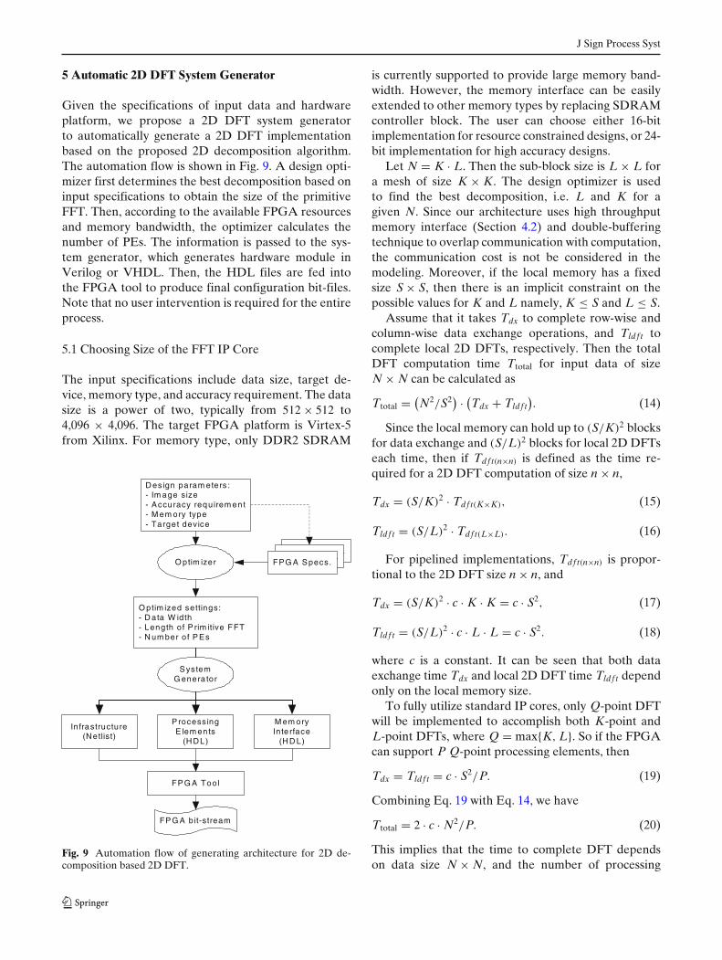
High Throughput Memory Interface While the PE ar-ray can finish computations very fast, the bottleneck isthe interface to external memory. Xilinx’s Multi-PortMemory Controller (MPMC), for instance, is a veryversatile controller supporting SDRAM/DDR/DDR2memory. However, its peak throughput is only 50%of a DDR2-SDRAM DIMM’s peak transfer rate. Toalleviate this bottleneck, we design a customized highthroughput memory interface.
The customized memory interface, as shown inFig. 8, has a 128-bit wide internal data-bus. Since theDDR2 SDRAM device has an operating frequency of200 MHz and an user application in FPGA runs at100 MHz, the memory interface operates at 200 MHzand has a 256-bit wide data bus between the interfaceand the application. This enables data transfer rates ofup to 256 bits at 100 MHz or 3,200 MB/s. Togetherwith double buffering technique on local memory, thecustomized memory interface enables us to completelyoverlap communication with computation and avoidany loss of performance due to communication bottle-neck. This memory interface can be ported onto anyFPGA board with SDRAM DIMMs.
Fig. 8 High throughputmemory interface. Memory Interface
(200 MHz)
BackendFIFOs
Commandinterface
DDR2SDRAM
Controller
AddressGeneration
DDR2SDRAMDIMM
(200 MHz) 25612812864
Local Memory (100 MHz)
J Sign Process Syst
5 Automatic 2D DFT System Generator
Given the specifications of input data and hardwareplatform, we propose a 2D DFT system generatorto automatically generate a 2D DFT implementationbased on the proposed 2D decomposition algorithm.The automation flow is shown in Fig. 9. A design opti-mizer first determines the best decomposition based oninput specifications to obtain the size of the primitiveFFT. Then, according to the available FPGA resourcesand memory bandwidth, the optimizer calculates thenumber of PEs. The information is passed to the sys-tem generator, which generates hardware module inVerilog or VHDL. Then, the HDL files are fed intothe FPGA tool to produce final configuration bit-files.Note that no user intervention is required for the entireprocess.
5.1 Choosing Size of the FFT IP Core
The input specifications include data size, target de-vice, memory type, and accuracy requirement. The datasize is a power of two, typically from 512 × 512 to4,096 × 4,096. The target FPGA platform is Virtex-5from Xilinx. For memory type, only DDR2 SDRAM
D esign param eters :- Im age size- Accuracy requirem ent- M em ory type- Target dev ice
FP G A Specs.FPG A Specs.
FPG A S pecs.O ptim izer
O ptim ized settings:- D ata W idth- Length of P rim itive FFT- N um ber of P Es
Infrastructure(N etlist)
S ystemG enera tor
P rocess ingE lem ents
(H D L)
M em oryInte rface
(H D L)
FP G A Tool
FP G A bit-stream
Fig. 9 Automation flow of generating architecture for 2D de-composition based 2D DFT.
is currently supported to provide large memory band-width. However, the memory interface can be easilyextended to other memory types by replacing SDRAMcontroller block. The user can choose either 16-bitimplementation for resource constrained designs, or 24-bit implementation for high accuracy designs.
Let N = K · L. Then the sub-block size is L × L fora mesh of size K × K. The design optimizer is usedto find the best decomposition, i.e. L and K for agiven N. Since our architecture uses high throughputmemory interface (Section 4.2) and double-bufferingtechnique to overlap communication with computation,the communication cost is not be considered in themodeling. Moreover, if the local memory has a fixedsize S × S, then there is an implicit constraint on thepossible values for K and L namely, K ≤ S and L ≤ S.
Assume that it takes Tdx to complete row-wise andcolumn-wise data exchange operations, and Tldf t tocomplete local 2D DFTs, respectively. Then the totalDFT computation time Ttotal for input data of sizeN × N can be calculated as
Ttotal = (N2/S2
) · (Tdx + Tldf t
). (14)
Since the local memory can hold up to (S/K)2 blocksfor data exchange and (S/L)2 blocks for local 2D DFTseach time, then if Tdf t(n×n) is defined as the time re-quired for a 2D DFT computation of size n × n,
Tdx = (S/K)2 · Tdf t(K×K), (15)
Tldf t = (S/L)2 · Tdf t(L×L). (16)
For pipelined implementations, Tdf t(n×n) is propor-tional to the 2D DFT size n × n, and
Tdx = (S/K)2 · c · K · K = c · S2, (17)
Tldf t = (S/L)2 · c · L · L = c · S2. (18)
where c is a constant. It can be seen that both dataexchange time Tdx and local 2D DFT time Tldf t dependonly on the local memory size.
To fully utilize standard IP cores, only Q-point DFTwill be implemented to accomplish both K-point andL-point DFTs, where Q = max{K, L}. So if the FPGAcan support P Q-point processing elements, then
Tdx = Tldf t = c · S2/P. (19)
Combining Eq. 19 with Eq. 14, we have
Ttotal = 2 · c · N2/P. (20)
This implies that the time to complete DFT dependson data size N × N, and the number of processing
J Sign Process Syst
Table 1 Resources required for Xilinx pipelined FFT IP.
FFT point 32 64 128 256
Virtex-4 24 bit DSP48 16 16 24 24BRAM 0 2 6 8
16 bit DSP48 6 6 9 9BRAM 0 1 3 4
Virtex-5 24 bit DSP48E 24 24 36 36BRAM 0 2 5 7
16 bit DSP48E 8 8 12 12BRAM 0 1 3 4
elements, P, which is, in turn, determined by the re-sources available on the FPGA.
As primitive FFT size increases, the number of DSPsand BRAMs both increase, as shown in Table 1. Foran FPGA with limited DSP and BRAM resources,we need to keep the value of Q as small as possible,so that more PEs can be accommodated. Since Q =max(K, L), and K · L = N, the smallest value of Q is√
N. However, if√
N is not an integer, we need tofind a factorization of N so that K and L are closeto each other. Once the optimal factorization is found,the length of the primitive FFT cores, Q, can be de-termined. For instance, if N = 1,024, Q = 32, and if Nincreases to 4,096, Q = 64.
5.2 Choosing the Number of PEs
After choosing the size of the FFT IP core, the numberof PEs is determined. Based on the hardware resourcesof the target FPGA and resources required by theFFT IP core given in Table 1, the 2D DFT generatorcalculates the maximum number of PEs, PRES, that canfit onto the FPGA. The external memory type/interfaceplays an equally important role in determining thenumber of PEs, since the pipelined Xilinx FFT IP [25]can input 1 datum/cycle. For instance, suppose thatthe data width of a complex datum is 32 (16 × 2) bits,and if FFT IP is running at 100 MHz, its data rate is400 MB/s. Now, let PBW be the maximum number ofPEs that can be supported by the available memorybandwidth. If the external memory is one DIMM ofDDR2-400 SDRAM, which can offer 3,200 MB/s datarate, up to 8 PEs can be supported, and PBW wouldbe set to “8”. In this case, the performance of the 2DDFT cannot be improved with more PEs. Eventually,the number of PEs is decided by the minimum ofPRES and PBW, i.e.
P = min{
PRES, PBW}. (21)
Once the design optimizer decides the number andtype of the primitive FFT IPs and memory partitioning,
the system generator generates all the required hard-ware modules, namely, infrastructure block, FFT coreblock and memory interface block. The infrastructureblocks such as UART and host connection are fixed,whereas other blocks are user specified and providedin a template format, with several parameters that areset based on decisions of the design optimizer. After thegeneration of these modules, scripts for Xilinx flow areproduced to run Xilinx tool automatically. Finally, theconfiguration bit file consisting of both hardware bit fileand software binaries are generated from FPGA tool.
6 Evaluation
In this section, the 2D DFT architecture generatedusing the DFT system generator is evaluated. First,the evaluation of high throughput memory interface ispresented in Section 6.1, and the resource utilizationis analyzed in Section 6.2. Then, the evaluation ofperformance for various input sizes is presented andcompared with existing solutions in Section 6.3. Finally,the numerical accuracy of the 2D DFT is analyzed inSection 6.4. For the evaluations, Xilinx 10.1 tool setand Modelsim 6.4 are used, and Virtex-5FX device isconsidered as the candidate FPGA device.
6.1 Memory Throughput for RC- and 2DDecomposition- Based Architectures
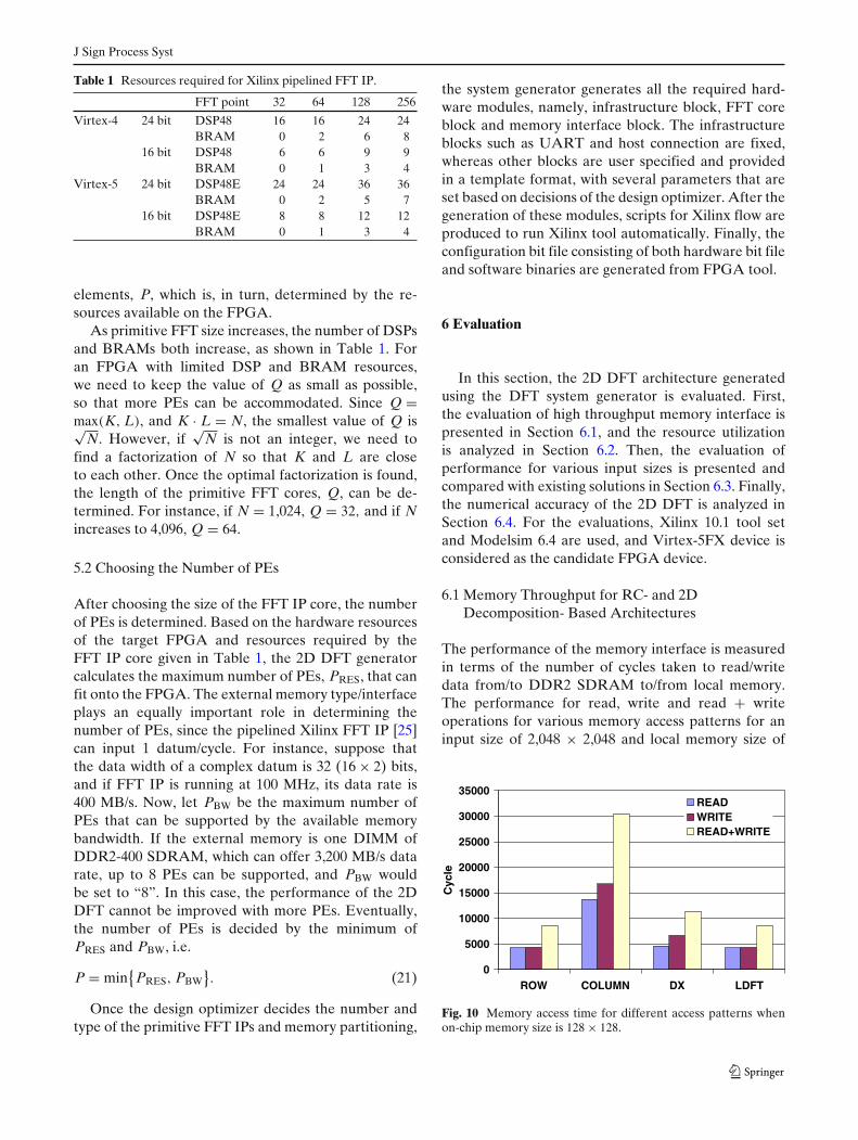
The performance of the memory interface is measuredin terms of the number of cycles taken to read/writedata from/to DDR2 SDRAM to/from local memory.The performance for read, write and read + writeoperations for various memory access patterns for aninput size of 2,048 × 2,048 and local memory size of
0
5000
10000
15000
20000
25000
30000
35000
ROW COLUMN DX LDFT
Cyc
le
READWRITEREAD+WRITE
Fig. 10 Memory access time for different access patterns whenon-chip memory size is 128 × 128.
J Sign Process Syst
Table 2 Resource utilizationand memory requirement fordifferent configurations.
Primitive FFT Bit width # of PEs DSP BRAM Slice LUTS Mem. BW(36 kbits) required (MB/s)
32-point FFT 16 bits 4 PEs 36 137 25,536 1,6008 PEs 72 137 35,238 3,200
16 PEs 144 145 54,442 6,40024 bits 4 PEs 112 145 33,294 3,200
8 PEs 224 145 46,326 6,40064-point FFT 16 bits 4 PEs 36 139 26,882 1,600
8 PEs 72 141 37,958 3,20024 bits 4 PEs 112 149 34,991 3,200
8 PEs 224 153 50,132 6,400
128 × 128 is shown in Fig. 10. It can be observed thatcolumn access is much slower compared to other accesspatterns, and hence it would be the bottle-neck for di-rect RC method. On the contrary, data exchange (DX)and local DFT (LDFT) are both row-wise accesses.Therefore, the proposed 2D DFT avoids the perfor-mance penalty caused by column access and hence canachieve a higher performance.
6.2 Resource Utilization
The resource utilization of the PEs (Xilinx FFT IPs,complex multipliers, and the control units) and thememory requirement in terms of bandwidth, are sum-marized in Table 2. This evaluation is based onthe device XC5FX200T, which has 384 DSP slices,456 BRAMs (16 Mbs), 30,720 logic slices, and 122,880slice LUTs. For large image sizes from 1,024 × 1,024through 4,096 × 4,096, the size of the FFT IP can beeither 32-point or 64-point. The data representationcan be either 16-bit or 24-bit. The infra-structure blockuses fixed number of resources of 8,149 logic slices and47 BRAMs including TEMAC for host interface. Weassume the operating frequency of the IPs is 100 MHzand the external memory device to be one DDR2-400SDRAM DIMM operating at 200 MHz.
From Table 2, we see that the number of BRAMsand Slice LUTs utilized by 64-point FFT are slightlyhigher than 32-point FFT, though the number of DSP
Table 3 Performance for different input sizes.
Input size Primitive # of PE Computation Frametime (ms) rates
1,024 × 1,024 32PT FFT 8 5.4 1824 10.7 92
2,048 × 2,048 64PT FFT 8 22.4 444 43.4 23
4,096 × 4,096 64PT FFT 8 90.4 114 174.3 5
resources utilized is the same for both the cases. Thenumber of DSP resources and the memory bandwidthrequired increase almost linearly with the numberof PEs. Also, there is a large increase in DSP re-sources and memory bandwidth, when the data-widthis changed from 16-bit to 24-bit.
From Table 2 we also see that the target FPGA canfit either 16 32-point FFT cores with 16-bit data width,or 8 32-point FFT cores whith 24-bit data width, or 864-point FFT core with 16-bit, or 8 64-point FFT coreswith 32-bit data width. The DSP resource requirementfor the 16 FFT cores (32-point and 64-point) with 24-bit data representation exceeds that supported by theVirtex5 FPGA and hence cannot fit in the device. Also,the configuration with 16 64-point FFT cores with 16-bitdata width cannot be supported due to local memoryconstraints. Thus, for both cases, the 2D DFT systemgenerator (see Section 5) would set PRES as “8”. Notethat PRES could be higher for other FPGAs with largercapacities.
Table 2 also list the required bandwidth for eachconfiguration, and based on the table, the 2D DFTsystem generator is able to determine PBW. For exam-ple, if we have 1 DIMM of DDR2-400 SDRAM witha bandwidth of 3200 MB/s, then for 64-point FFT IPwith 24-bit representation, PBW = 4. Although PRES
in this case is “8”, the final number of PEs is “4”,based on Eq. 21. However if we have 2 DIMMs ofDDR2-400 SDRAM, then the available memory band-width is 6,400 MB/s, and the final number of PEs is8. Note that PBW could be higher if more DIMMS ora faster memory device, such as DDR2-800 SDRAM,is used.
Table 4 Performance comparison for different architectures forinput size 2048 × 2048.
RC Transpose 2D-DEC
Computation time (ms) 44.0 30.4 22.4Frame rates 23 33 44
J Sign Process Syst
Fig. 11 Comparison of the computation times (normalized toRC-based method) for different image sizes.
6.3 Comparison of Timing Performance
Table 3 shows the performance of the 2D DFT architec-ture for different input sizes and different architectureconfigurations. The performance is specified in termsof frame rate, which refers to the number of frames ofinput data that the 2D DFT architecture can processin a second. The size of the FFT primitive is chosenby the design optimizer (see Section 5). It can be seenthat the performance is inversely proportional to theinput data size, but directly proportional to the numberof PEs.
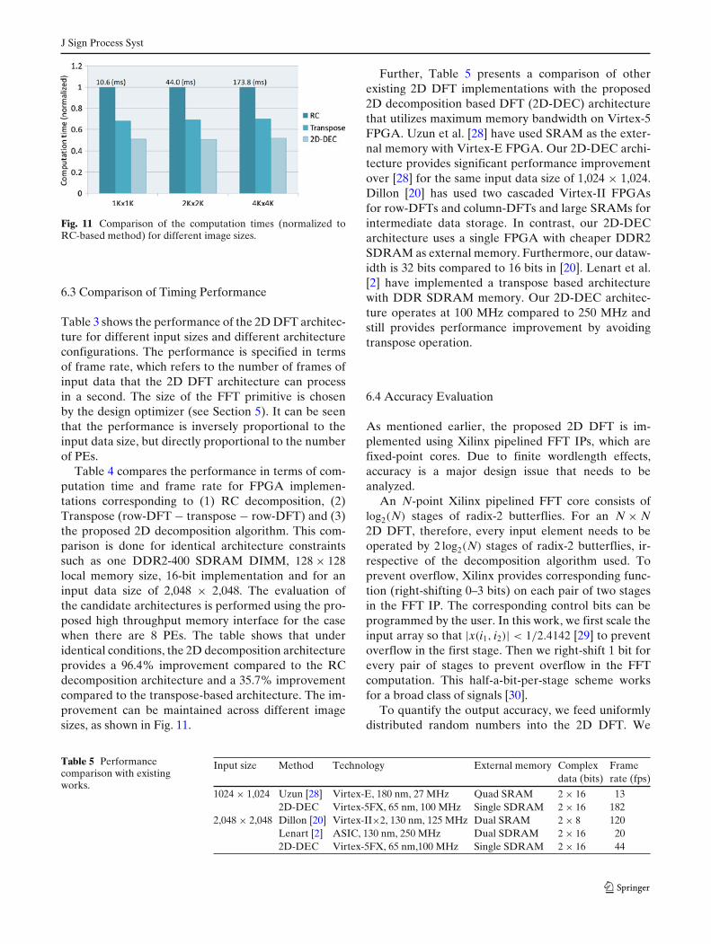
Table 4 compares the performance in terms of com-putation time and frame rate for FPGA implemen-tations corresponding to (1) RC decomposition, (2)Transpose (row-DFT − transpose − row-DFT) and (3)the proposed 2D decomposition algorithm. This com-parison is done for identical architecture constraintssuch as one DDR2-400 SDRAM DIMM, 128 × 128local memory size, 16-bit implementation and for aninput data size of 2,048 × 2,048. The evaluation ofthe candidate architectures is performed using the pro-posed high throughput memory interface for the casewhen there are 8 PEs. The table shows that underidentical conditions, the 2D decomposition architectureprovides a 96.4% improvement compared to the RCdecomposition architecture and a 35.7% improvementcompared to the transpose-based architecture. The im-provement can be maintained across different imagesizes, as shown in Fig. 11.
Further, Table 5 presents a comparison of otherexisting 2D DFT implementations with the proposed2D decomposition based DFT (2D-DEC) architecturethat utilizes maximum memory bandwidth on Virtex-5FPGA. Uzun et al. [28] have used SRAM as the exter-nal memory with Virtex-E FPGA. Our 2D-DEC archi-tecture provides significant performance improvementover [28] for the same input data size of 1,024 × 1,024.Dillon [20] has used two cascaded Virtex-II FPGAsfor row-DFTs and column-DFTs and large SRAMs forintermediate data storage. In contrast, our 2D-DECarchitecture uses a single FPGA with cheaper DDR2SDRAM as external memory. Furthermore, our dataw-idth is 32 bits compared to 16 bits in [20]. Lenart et al.[2] have implemented a transpose based architecturewith DDR SDRAM memory. Our 2D-DEC architec-ture operates at 100 MHz compared to 250 MHz andstill provides performance improvement by avoidingtranspose operation.
6.4 Accuracy Evaluation
As mentioned earlier, the proposed 2D DFT is im-plemented using Xilinx pipelined FFT IPs, which arefixed-point cores. Due to finite wordlength effects,accuracy is a major design issue that needs to beanalyzed.
An N-point Xilinx pipelined FFT core consists oflog2(N) stages of radix-2 butterflies. For an N × N2D DFT, therefore, every input element needs to beoperated by 2 log2(N) stages of radix-2 butterflies, ir-respective of the decomposition algorithm used. Toprevent overflow, Xilinx provides corresponding func-tion (right-shifting 0–3 bits) on each pair of two stagesin the FFT IP. The corresponding control bits can beprogrammed by the user. In this work, we first scale theinput array so that |x(i1, i2)| < 1/2.4142 [29] to preventoverflow in the first stage. Then we right-shift 1 bit forevery pair of stages to prevent overflow in the FFTcomputation. This half-a-bit-per-stage scheme worksfor a broad class of signals [30].
To quantify the output accuracy, we feed uniformlydistributed random numbers into the 2D DFT. We
Table 5 Performancecomparison with existingworks.
Input size Method Technology External memory Complex Framedata (bits) rate (fps)
1024 × 1,024 Uzun [28] Virtex-E, 180 nm, 27 MHz Quad SRAM 2 × 16 132D-DEC Virtex-5FX, 65 nm, 100 MHz Single SDRAM 2 × 16 182
2,048 × 2,048 Dillon [20] Virtex-II×2, 130 nm, 125 MHz Dual SRAM 2 × 8 120Lenart [2] ASIC, 130 nm, 250 MHz Dual SDRAM 2 × 16 202D-DEC Virtex-5FX, 65 nm,100 MHz Single SDRAM 2 × 16 44
J Sign Process Syst
Table 6 SNR(dB) of proposed 2D DFT, where the input set is drawn from uniformly distributed random number and |x(i1, i2)| <
1/2.4142.
DFT size 64 × 64 128 × 128 256 × 256 512 × 512 1,024 × 1,024 2,048 × 2,048
16 bit 70.56 69.94 69.67 69.36 68.72 67.7220 bit 94.50 94.50 93.92 92.97 92.16 91.5924 bit 118.77 118.17 117.52 117.15 116.81 116.03
adopt a commonly used criterion, Signal-to-Noise-Ratio (SNR), which is defined as:
SNR(dB) = 10 log10
Poutput
Pquantnoise,
where Poutput is average output power, and Pquantnoise isacquired by comparing the hardware output with Mat-lab floating point results. The SNR results for randomlygenerated input data are listed in Table 6.
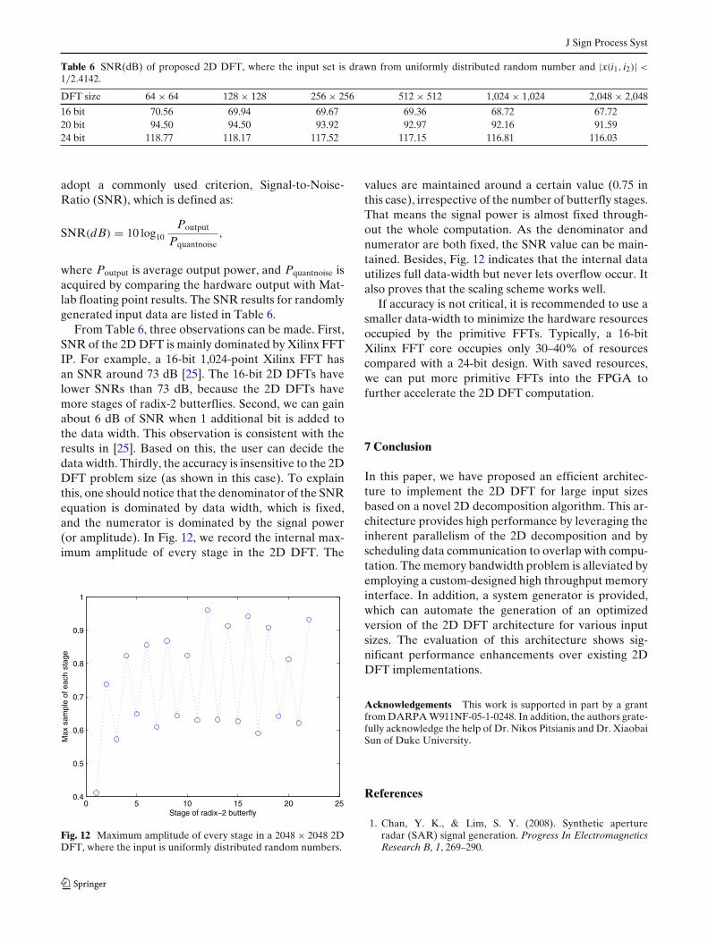
From Table 6, three observations can be made. First,SNR of the 2D DFT is mainly dominated by Xilinx FFTIP. For example, a 16-bit 1,024-point Xilinx FFT hasan SNR around 73 dB [25]. The 16-bit 2D DFTs havelower SNRs than 73 dB, because the 2D DFTs havemore stages of radix-2 butterflies. Second, we can gainabout 6 dB of SNR when 1 additional bit is added tothe data width. This observation is consistent with theresults in [25]. Based on this, the user can decide thedata width. Thirdly, the accuracy is insensitive to the 2DDFT problem size (as shown in this case). To explainthis, one should notice that the denominator of the SNRequation is dominated by data width, which is fixed,and the numerator is dominated by the signal power(or amplitude). In Fig. 12, we record the internal max-imum amplitude of every stage in the 2D DFT. The
0 5 10 15 20 250.4
0.5
0.6
0.7
0.8
0.9
1
Stage of radix−2 butterfly
Max
sam
ple
of e
ach
stag
e
Fig. 12 Maximum amplitude of every stage in a 2048 × 2048 2DDFT, where the input is uniformly distributed random numbers.
values are maintained around a certain value (0.75 inthis case), irrespective of the number of butterfly stages.That means the signal power is almost fixed through-out the whole computation. As the denominator andnumerator are both fixed, the SNR value can be main-tained. Besides, Fig. 12 indicates that the internal datautilizes full data-width but never lets overflow occur. Italso proves that the scaling scheme works well.
If accuracy is not critical, it is recommended to use asmaller data-width to minimize the hardware resourcesoccupied by the primitive FFTs. Typically, a 16-bitXilinx FFT core occupies only 30–40% of resourcescompared with a 24-bit design. With saved resources,we can put more primitive FFTs into the FPGA tofurther accelerate the 2D DFT computation.
7 Conclusion
In this paper, we have proposed an efficient architec-ture to implement the 2D DFT for large input sizesbased on a novel 2D decomposition algorithm. This ar-chitecture provides high performance by leveraging theinherent parallelism of the 2D decomposition and byscheduling data communication to overlap with compu-tation. The memory bandwidth problem is alleviated byemploying a custom-designed high throughput memoryinterface. In addition, a system generator is provided,which can automate the generation of an optimizedversion of the 2D DFT architecture for various inputsizes. The evaluation of this architecture shows sig-nificant performance enhancements over existing 2DDFT implementations.
Acknowledgements This work is supported in part by a grantfrom DARPA W911NF-05-1-0248. In addition, the authors grate-fully acknowledge the help of Dr. Nikos Pitsianis and Dr. XiaobaiSun of Duke University.
References
1. Chan, Y. K., & Lim, S. Y. (2008). Synthetic apertureradar (SAR) signal generation. Progress In ElectromagneticsResearch B, 1, 269–290.
J Sign Process Syst
2. Lenart, T., Gustafsson, M., & Owall, V. (2008). A hardwareacceleration platform for digital holographic imaging. Journalof Signal Processing System, 52(3), 297–311.
3. Frigo, M., & Johnson, S. (1998). FFTW: An adaptive softwareof the FFT. Proceedings of the IEEE International Conferenceon Acoustics, Speech, and Signal Processing, 3, 1381–1384.
4. Püschel, M., et al. (2005). SPIRAL: Code generation for DSPtransforms. Proceedings of the IEEE, 93(2), 232–275.
5. Intel Math Kernel Library (MKL). http://software.intel.com/en-us/intel-mkl/.
6. Intel Integrated Performance Primitives (IPP). http://software.intel.com/en-us/intel-ipp/.
7. Franchetti, F., et al. (2009). Discrete Fourier transform onmulticore. IEEE Signal Processing Magazine, Special Issueon “Signal Processing on Platforms with Multiple Cores”,26(6), 90–102.
8. Eleftheriou, M., et al. (2005). Scalable framework for 3DFFTs on the blue gene/l supercomputer: Implementation andearly performance measurements. IBM Journal of Researchand Development, 49, 457–464.
9. Fang, B., et al. (2007). Performance of the 3D FFT on the 6Dnetwork torus QCDOC parallel supercomputer. ComputerPhysics Communications, 176(8), 531–538.
10. Cooley, J. W., & Tukey, J. W. (1965). An algorithm for themachine computation of complex Fourier series. Mathematicsof Computation, 19, 297–301.
11. Yeh, W.-C., & Jen, C.-W. (2003). High-speed and low-powersplit-radix FFT. IEEE Transactions on Signal Processing, 51,864–874.
12. Lin, Y.-W., et al. (2005). A 1-GS/s FFT/IFFT processor forUWB applications. IEEE Journal of Solid-State Circuits, 40,1726–1735.
13. PowerFFT ASIC. http://www.eonic.com/index.asp?item=32.14. Baas, B. (1999). A low-power, high-performance, 1024-point
FFT processor. IEEE Journal OF Solid-state Circuits, 34(3),380–387.
15. Uzun, I., Amira, A., & Bouridane, A. (2005). FPGA imple-mentations of fast Fourier transforms for real-time signal andimage processing. IEE Proceedings. Vision, Image, and SignalProcessing, 152(3), 283–296.
16. Sasaki, T., et al. (2005). Reconfigurable 3D-FFT processor forthe car-parrinello method. The Journal of Computer Chem-istry, Japan, 4(4), 147–154.
17. D’Alberto, P., et al. (2007). Generating FPGA acceleratedDFT libraries. In IEEE symposium on f ield-programmablecustom computing machines (FCCM) (pp. 173–184).
18. Kumhom, P., Johnson, J., & Nagvajara, P. (2000). Design, op-timization, and implementation of a universal FFT processor.In IEEE ASIC/SOC conference (pp. 182–186). IEEE.
19. Milder, P. A., et al. (2008). Formal datapath representa-tion and manipulation for implementing DSP transforms. InDesign automation conference (DAC) (pp. 385–390).
20. Dillon, T. (2001). Two virtex-II FPGAs deliver fastest, cheap-est, best high-performance image processing system. XilinxXcell Journal, 41, 70–73.
21. Milder, P. A., et al. (2007). Discrete Fourier transform com-piler: From mathematical representation to ef f icient hardware.Carnegie Mellon University, Tech. Rep. CSSI-07-01.
22. Van Loan, C. (1992). Computational framework of the fastFourier transform. Philadelphia, PA: SIAM.
23. Pitsianis, N. P. (1997). The Kronecker product in approxima-tion and fast transform generation. Dissertation for the degreeof Doctor of Philosophy, Cornell University.
24. Wu, H. R., & Paoloni, F. J. (1989) The structure of vec-tor radix fast Fourier transforms. IEEE Transactions onAcoustics, Speech, and Signal Processing, 37(9).
25. FFT Xilinx Logicore. http://www.xilinx.com/products/ipcenter/FFT.htm.
26. Hard tri-mode MAC. http://www.xilinx.com/products/design_resources/conn_central/protocols/gigabit_ethernet.htm.
27. lwIP. http://www.sics.se/~adam/lwip/.28. Uzun, I., Amira, A., & Bouridane, A. (2005). FPGA imple-
mentations of fast Fourier transforms for real-time signal andimage processing. IEE Proceedings. Vision, Image, and SignalProcessing, 152(3), 283–296.
29. Elam, D., & Lovescu, C. (2003). A block f loating point im-plementation for an N-point FFT on the TMS320C55X DSP.Application Report SPRA948, Texas Instruments, Dallas,Texas, USA.
30. Welch, P. (1969). A fixed-point fast Fourier transform erroranalysis. IEEE Transactions on Audio and Electroacoustics,17(2), 151–157.
Chi-Li Yu (S’10) received the BS and MS degrees in electricalengineering from National Central University, Taiwan, in 1998and 2000, respectively. From 2001 to 2005, he was an associateengineer in Industrial Technology Research Institute (ITRI),Taiwan. Currently, he is a PhD candidate in School of Electrical,Computer and Energy Engineering, Arizona State University,Tempe. His research interests include high-performance/low-power algorithm-architecture co-design for DSP, image process-ing, and communication applications. He is a student member ofthe IEEE.
Jung-Sub Kim (S’07) received the BS and MS degrees in elec-trical engineering from Yonsei University, Seoul, Korea, in 1995and 1997, respectively, and the PhD degree in electrical engineer-ing from the Pennsylvania State University in 2008. From 1997

J Sign Process Syst
to 2003, he was with the Embedded System Laboratory, R&DCenter, LG Industrial System, Anyang, Korea. Currently, he isa senior engineer with Architecture Research Laboratory, DMCR&D Center, Samsung Electronics, Suwon, Korea. His researchinterests include high-performance reconfigurable systems designand reliable circuit design. He is a student member of the IEEE.
Lanping Deng received the BS and MS degrees in electricalengineering from Tsinghua University, Beijing, China, in 2003and 2005, respectively. In 2009, he received the PhD degree inelectrical engineering from Arizona State University, Tempe. Hisresearch interests include hardware-software codesign, FPGAbased accelerator design, and EDA tool design.
Srinidhi Kestur (S’10) received the BE degree in Electronicsand Communication Engineering from R V College of Engi-neering, India in 2005. From 2005 to 2006, he was a softwareengineer in the DSP software group at Analog Devices,
Bangalore. Currently, he is a PhD candidate in Electrical Engi-neering at Pennsylvania State University, University Park. Hisresearch interests are in high-performance reconfigurable sys-tems design for applications in signal processing, vision and high-performance computing. He is a student member of the IEEE.
Vijaykrishnan Narayanan is a professor of computer scienceand engineering at The Pennsylvania State University, UniversityPark. His research interests are in computer architecture, embed-ded systems, and nanoarchitectures.
Chaitali Chakrabarti (SM’02) is a professor of Electrical En-gineering at Arizona State University, Tempe. Her researchinterests are in the areas of low-power embedded systems designand algorithm-architecture co-design of signal processing, imageprocessing, and communication systems.
Related Documents