1 FOLWER-NORDHEIM TUNNELING IN METAL- INSULATOR-METAL VAN DER WAALS HETEROSTRUCTURES NG SHIUAN JUN SUPERVISOR: ASSOCIATE PROFESSOR EDA GOKI A THESIS SUBMITTED IN PARTIAL FULFILMENT OF THE REQUIREMENTS FOR THE DEGREE OF BACHELOR OF SCIENCE WITH HONOURS DEPARTMENT OF PHYSICS NATIONAL UNIVERSITY OF SINGAPORE 2019

Welcome message from author
This document is posted to help you gain knowledge. Please leave a comment to let me know what you think about it! Share it to your friends and learn new things together.
Transcript
1
FOLWER-NORDHEIM TUNNELING IN METAL-
INSULATOR-METAL VAN DER WAALS
HETEROSTRUCTURES
NG SHIUAN JUN
SUPERVISOR: ASSOCIATE PROFESSOR EDA GOKI
A THESIS SUBMITTED IN PARTIAL FULFILMENT OF THE
REQUIREMENTS FOR THE DEGREE OF BACHELOR OF
SCIENCE WITH HONOURS
DEPARTMENT OF PHYSICS
NATIONAL UNIVERSITY OF SINGAPORE
2019

2
Abstract
The heterostructures of two-dimensional (2D) materials are considered promising
candidates for future electronic devices. In this work, we manifest the Fowler-
Nordheim (FN) tunnelling characteristics through thin layer boron nitride (BN) by
fabricating metal-insulator-metal (MIM) heterostructure devices consisting of BN
sandwiched by 2D metals, including few layer graphene (FLG) and high work
function transition metal dichalcogenides (TMDCs): niobium disulphide (NbS2)
and tantalum disulphide (TaS2). We argue that the main charge carrier is holes
considering the band diagram of heterostructures. I-V measurements of these MIM
devices show that the barrier heights for holes tunnelling through BN depend on
the work function of 2D metals. The tunnelling barrier height for holes we extracted
from the FN plot for TaS2 is smaller than that of FLG, which is consistent with the
expected band alignment. However, the results for NbS2 are opposite to the
prediction, which we attributed to the possible oxidation of the surface of the 2D
metal. This study could provide effective ideas to modify the tunnelling features of
vertical heterostructures for their prospective role in next generation high
performance electronic devices.
3
Acknowledgements
First and foremost, I would like to express my deepest gratitude towards my supervisor, Associate
Professor Eda Goki, for accepting me into his lab for my FYP. I am grateful for his guidance and
ideas throughout this project. Prof Eda constantly allows us to have complete freedom to venture
new ideas which gave us ample space for our personal development and has allowed me to find
joy in working in the lab, fabricating new devices. Therefore, I am very honoured to be a student
under him and is very thankful for the trust that he has in me.
Next, I am really grateful for my mentor, Mr Wang Jun Yong for his patience and guidance. He
has patiently guided me through various phases of the project, not only teaching me how to use
the various lab equipment but also taught me to remain positive even during setbacks. Despite his
busy schedule, he always make it a point to check on my progress and provide necessary feedbacks.
This thesis and project would not have been possible without his knowledge and guidance.
I would also like to express my gratitude towards everyone in Eda’s Lab, particularly to those
always in lab, for providing advices, motivation and joy through times when it was necessary. Not
forgetting to mention the other FYP students under Eda’s Lab, for always sharing resources and
always being there for each other.

4
TABLE OF CONTENTS
ABSTRACT .................................................................................................................................. 2
ACKNOWLEDGEMENTS .......................................................................................................... 3
LIST OF TABLES ........................................................................................................................ 5
LIST OF FIGURES ...................................................................................................................... 5
1. INTRODUCTION .................................................................................................................. 6
1.1 2D MATERIALS ........................................................................................................ 6
1.2 TUNNELLING THROUGH AN INSULATOR ........................................................ 8
1.3 TUNNELLING THROUGH 2D MATERIALS ......................................................... 9
1.4 MOTIVATION ........................................................................................................... 11
2. METHODOLOGY ................................................................................................................. 14
3. RESULTS AND DISCUSSION ............................................................................................ 17
3.1 CHARACTERIZATION – RAMAN SPECTROSCOPY .......................................... 17
3.2 CHARACTERIZATION – ATOMIC FORCE MICROSCOPY (AFM) .................. 18
3.3 I-V CHARACTERISTICS .......................................................................................... 19
4. CONCLUSION ....................................................................................................................... 26
REFERENCES ............................................................................................................................. 27
5
List of Tables
Table 1 Comparison of observed Raman shift peak frequencies for exfoliated TaS2 and NbS2 against
literature. ..................................................................................................................................................... 18
Table 2 Barrier height for holes 𝝓𝑩𝒉 and for electrons 𝝓𝑩𝒆 calculated from FNT in MIM devices ....... 21
List of Figures
Figure 1 Band diagram illustrating the energy barrier in FN tunnelling there is (a) no applied bias (b)
applied bias. Note: the dotted arrow represents the charge carrier movement. ............................................ 9
Figure 2 (a) I-V measurements of h-BN of various thicknesses (N=layer number) Adapted11(redo) (b)
Energy diagram in direct tunnelling regime (c) Energy diagram in FN tunnelling regime. ....................... 11
Figure 3 (a) Work function linear dependence on barrier height (b) Schematic of heterostrucure stack.
Adapted21 .................................................................................................................................................... 12
Figure 4 Optical microscope images of (a) Gr/h-BN/Gr device (b) TaS2/h-BN/TaS2 device (c) NbS2/h-
BN/NbS2 device (d) Cross-sectional schematic representation of MIM heterostructure device. ................ 16
Figure 5 Raman Spectrum for (a) 2H-TaS2 (b) 3R-NbS2 .......................................................................... 17
Figure 6 AFM image of 7.3nm thick h-BN used as a point of reference .................................................... 18
Figure 7 Current vs Voltage, I-V characteristics of MIM structures ........................................................... 19
Figure 8 FN plot derived from I-V curves for (a) TMDCs MIM devices (b) Graphene MIM devices. ...... 20
Figure 9 FN tunnelling diagram representing electron/hole barrier. ........................................................... 22
Figure 10 Visual fitting of graphene (Gr) and TaS2 into extrapolated known linear regression of barrier
height against work function . ..................................................................................................................... 23
6
1. Introduction
The discovery of graphene in 2004 brought about by Geim and Novoselov1 has heralded the advent
of innovative 2D materials. Isolated stable, one-atom-thick 2D layers could be obtained from van
der Waals solid crystals, which exhibit unique and fascinating physical characteristics as well as
many innovative routes for applications. Since there is no dangling bond in the 2D layered
materials, different atomically thin 2D materials can be stacked together to form van der Waals
heterostructures with various functionalities. Among them, MIM tunnelling devices show promise
in electronic devices with a high on-off ratio. Even though the contact between different layers in
a traditional 3D heterojunctions has been investigated, the behaviour of carrier flow through 2D
interfaces could be quite unconventional, which leaves us much room to explore.
1.1 2D Materials
Atomically thin 2D materials such as graphene2,3, hexagonal boron nitride (h-BN)4,5, and transition
metal dichalcogenides6 (TMDCs) have been intensively studied the past decade due to the
capability to assemble multiple 2D materials with complementary properties into layered
heterogeneous structures.
h-BN is a typical insulating layered material with a wide band gap ~6.0 eV, high thermal stability,
an atomically flat surface and ideally no dangling bonds7,8. With a honeycomb structure based on
sp2 covalent bonds similar to graphene, bulk h-BN has first gained tremendous attention being an
exceptional substrate for graphene with an atomically smooth surface. 2D h-BN in the form of
few-layer crystal, has then appeared as a fundamental building block of van der Waals

7
heterostructures. In addition to its high dielectric strength and electrical reliability, h-BN is
considered an apt choice as a tunnelling barrier9,10.
A single graphene layer is only a one-atom-thick layer of sp2-bonded carbon in a tightly bound
honeycomb crystal structure. Layers of graphene stacked on top of each other form graphite (bulk
form), with an interplanar spacing of 0.335 nanometres (nm)8. The separate layers of graphene in
graphite are held together by van der Waals forces, which can be cleaved during exfoliation of
graphene from bulk graphite.
Bulk crystals of transition metal dichalcogenides (TMDCs) have been studied for decades. A
TMDC is basically made of weakly interacting stacks of 2D MX2 where M is a transition metal
from groups IV, V, or VI and X is a chalcogen atom like S, Se, or Te. The 2D layered structure of
MX2 has increased attractiveness after 2D graphene came about.
Tantalum disulphide (TaS2) is part of the TMDC family. TaS2 composition is that of covalently
bonded S–Ta–S planes that stack upon each other. It exists as a variety of polytypic phases that
comes from the distinct in-plane Ta coordination spheres attached to S2− ligands and by the
stacking periodicity of individual planes. For example, the 1T and 2H polytypes unit cells exists
in the form of one octahedral and two trigonal bi-pyramidal Ta-coordinated layers, respectively.
Although previously it was extensively researched upon in the 1960s, 1T and 2H polytypes are
once again attracting major attention as they constitute ideal case studies for the investigation of
namely superconductivity11 and charge density waves (CDW)12.
Bulk NbS2 is not only known for its high work function but also for its superconductivity at low
temperature. The 2H-TaS2 polytype layer structure is a known metal at ambient conditions13.
8
Unlike the honeycomb crystal structure of graphene, NbS2 have layers of trigonal edge-sharing
prisms stacked onto each other. However, similar to graphene, the intra-layer bonding is primarily
covalent, whereas the sheets of layers are connected by van der Waals forces. Same as TaS2, there
exists different stacking configurations of NbS2 layers which to the formation of two polytypes -
hexagonal 2H-NbS2 with two NbS2 layers and rhombohedral 3R-NbS2 with three layers per unit
cell14. The 3R polymorph layer structure causes a strong anisotropy in the physical properties like
resistivity and compressibility and is a metal at ambient conditions15.
1.2 Tunnelling through an insulator
Field electron emission is centred on free electrons tunnelling through the surface barrier by having
a strong applied electric field to reduce the barrier’s height and width. The first scientific
explanation of field emission was proposed by Fowler and Nordheim in 1928 using the concept of
quantum tunnelling and is now widely known as the Fowler-Nordheim (FN) Law16:
𝐽𝐹𝑁(𝑉) =𝐴𝑒3
8𝜋ℎ𝜙𝐵
𝑚
𝑚∗ (𝑉
𝑑)
2
𝑒𝑥𝑝 (−8𝜋√2𝑚∗𝜙𝐵
32
3ℎ𝑒
𝑑
𝑉) (1)

9
where 𝐽𝐹𝑁, A, ϕB, e, m, m*, d, and h, are field-emission current density, effective contact area,
barrier height, electron charge, free electron mass, effective electron mass, barrier width, and
Planck’s constant respectively. This quantum mechanical tunnelling process is imperative in the
study of thin barriers such as those in metal-insulator junctions. There is another kind of tunnelling
that can occur across an insulator which is direct tunnelling – it occurs when the electrons tunnel
through when the barrier width is small and applied bias is low. Figure 1 left diagram represents
the charge carrier tunnelling that could occur without bias which is a representation of direct
tunnelling where electrons tunnel through without the aid of a field. While the diagram on the right
represents FN tunnelling where the barrier height is effectively pulled down by an electric field
(applied voltage) to assist in charge carrier injection through the insulator.
1.3 Tunnelling through 2D Materials
The interfaces in 2D materials are different from the 3D situation due to the disparate nature of the
contacts. As a typical example, in 2D materials and their interfaces, Fermi-level pinning plays a
significant role compared with 3D interfaces. Within a metal/semiconductor contact, the
Figure 1 Band diagram illustrating the energy barrier in FN tunnelling there is (a) no applied bias (b) applied
bias. Note: the dotted arrow represents the charge carrier movement.
Figure 2 Band diagram illustrating the energy barrier in FN tunnelling there is (a) no applied bias (b) applied
bias. Note: the dotted arrow represents the charge carrier movement.

10
wavefunction of an electron at the interface of the contact must match17. Since the Fermi levels of
the two materials must match at the interface, metal induced gap states (MGIS) arising from direct
chemical bonding or surface states must exist18. These highly dense states would then be able to
take in a large amount of charge from the metal, effectively shielding the semiconductor from the
influence of the metal. As a result, the semiconductor's bands would unavoidably align to a location
relative to the surface states (band bending) which are essentially pinned to the Fermi level (due
to their high density), all without influence from the metal. In the typical 3D metal-2D
semiconductor interface, the conductance of 2D semiconductors, MoS2 for example, can rarely be
tuned by the work function of the 3D metals19. This raises a question, would the carrier in the
interface of a 2D metal and 2D insulator follow the band diagram or have a similar pinning effect.
As mentioned before, there are two main types of quantum tunnelling process when considering
tunnelling through a 2D insulator at room temperature - direct tunnelling and Fowler-Nordheim
tunnelling. However, as we are considering the 2D plane where the charge carrier injection into
the insulator is travelling across a short distance, the thickness of the insulator affects whether
direct or FN tunnelling dominate, illustrated in Figure 3. A very thin h-BN would result in direct
tunnelling to be observed instead of FN tunnelling. In order to examine FN tunnelling explicitly,
it is thus important that we have control over the thickness of the 2D insulator. For instance, it has
been reported that mono-, bi- and tri-layer h-BN displays direct tunnelling current in the low-bias
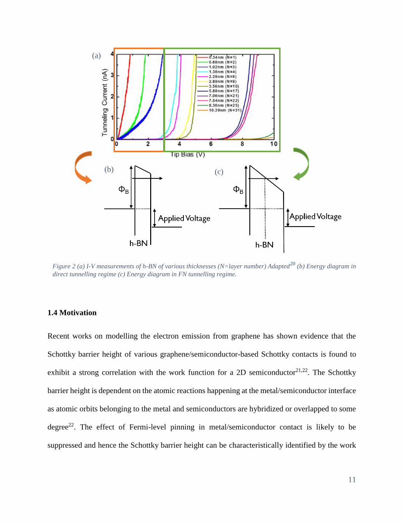
regime while h-BN of 4 layers and more displays FN tunnelling characteristics20. This phenomena
can be easily explained with the diagrams in Figure 2(b) and 2(c) where the barrier width becomes
so thin such that the FN tunnelling becomes insignificant and direct tunnelling of charge carriers
occur instead.
11
1.4 Motivation
Recent works on modelling the electron emission from graphene has shown evidence that the
Schottky barrier height of various graphene/semiconductor-based Schottky contacts is found to
exhibit a strong correlation with the work function for a 2D semiconductor21,22. The Schottky
barrier height is dependent on the atomic reactions happening at the metal/semiconductor interface
as atomic orbits belonging to the metal and semiconductors are hybridized or overlapped to some
degree22. The effect of Fermi-level pinning in metal/semiconductor contact is likely to be
suppressed and hence the Schottky barrier height can be characteristically identified by the work
Figure 2 (a) I-V measurements of h-BN of various thicknesses (N=layer number) Adapted20
(b) Energy diagram in
direct tunnelling regime (c) Energy diagram in FN tunnelling regime.
(a)
(b)
(c)

12
function of 2D semiconductor for a given metal23–25. It would then seem interesting to look into
the dependence of barrier height on the work function of metal in 2D heterojunction contacts.
Thin film MIM tunnel devices have become a vital part in the design of integrated nano-
components for a diversity of high-speed applications such as hot electron transistors26–28 and
optical rectenna for infrared energy harvesting in solar cell technology9,29. The classic way to attain
high-speed rectification in a MIM tunnelling device is through charge transport dominated by FN
tunnelling in conjunction with the use of metal electrodes with differing work functions which
produce asymmetric, polarity dependent charge carrier tunnelling barriers30.
Hattori and Nagashio published a recent paper on FN tunnelling through MIM devices on pure
evaporated metals and they have established the existence of Fermi level pinning effect at the h-
BN/metal interface23. Moreover, as shown from Figure 3 above, their group has identified that
there is a barrier height linear correlation to the work function of metal for 4 different metal/h-BN
contacts, presenting that a metal with a higher work function has a higher barrier height in FN
tunnelling through h-BN. However, more has to be analysed to make a conclusive statement,
especially with the case of 2D metallic TMDCs which have a different interface states when paired
with h-BN31,32. This inspires our work to investigate the FN tunnelling model barrier height
Figure 3 (a) Work function linear dependence on barrier height (b) Schematic of heterostrucure stack. Adapted 23

13
dependence on the work function of 2D metallic TMDCs, especially high work function 2D
metallic TMDCs.

14
2. Methodology
For the first step in the fabrication of these MIM heterostructures, h-BN graphene, NbS2 and TaS2
were first mechanically exfoliated from bulk single crystals onto separate Si/SiO2 wafers. Prior to
exfoliation, NbS2 and TaS2 were grown using the chemical vapour transport technique33,34 where
stoichiometric M (either Nb or Ta) and S is sealed in a quartz tube and heated at elevated
temperatures for 10–14 days to create the bulk crystals. As the TMDCs have different existing
crystalline phases where they could exhibit semiconductor or metallic properties, they were first
characterized using room temperature Raman spectroscopy to determine its crystalline phase to
ascertain if the exfoliated 2D material is indeed in the metallic phase as desired – 3R-NbS2 and
2H-TaS2.
As FNT takes place noticeably at high bias voltages whereby an increase in the barrier height could
be a result of increasing interlayer film thickness of h-BN20, it was necessary to screen the h-BN
samples for a benchmark uniform thickness to be used throughout all MIM devices. Hence,
samples of thin h-BN flakes, with slightly differing opacity of blue when seen under the optical
microscope, had their thickness measured using Atomic Force Microscopy (AFM) - tapping mode.
Through optical contrast and visual analysis4, we were able to distinguish and categorize the
thickness of h-BN flakes depending on their subtle colour differences.
To construct the 3 layered heterostructure, the pick-up dry transfer method35 was used. A layer of
polypropylene carbonate (PPC) was spin-coated on a polydimethylsiloxane (PDMS) glass stamp,
and the stamp is then attached to a micromanipulator with the PPC layer facing the Si/SiO2 wafers
containing the flakes we require for the heterostructure stack. Through the use of an optical
microscope to perceive the depth, the stamp is lowered slowly till the PPC layer reaches the

15
vicinity of the desired flake. This movement cannot be overly fast to prevent wrinkling or buckling
of the sample on contact. In order to bring the substrate to slowly contact the desired flake, slow
tuning of applied heat is necessary to melt the thin layer of PPC till the desired flake is
encompassed by PPC before turning off the heat. After sufficient cooling for approximately 15-20
minutes, the next step is to gently raise the micromanipulator stage and peel the PDMS stamp off
the Si/SiO2 wafers. After the top layer of the MIM heterostructure is picked up, the next layer can
be picked up with the same process after aligning with the next flake using the optical microscope.
The complete heterostructure can then be released onto SiO2 by melting the PPC layer onto SiO2
with application of high heat. Any PPC residue were then removed with acetone and isopropyl
alcohol. It has to be noted that in the fabrication of our device, h-BN serves as the tunnelling barrier,
hence the top and bottom metal layer must not touch each other and appropriate alignment is
necessary to ensure successful device fabrication is achieved.
For our MIM tunnel devices, sacrificial poly-methyl methacrylate (PMMA) were lithographically
patterned to the tri-layered heterostructure by electron beam lithography, leaving the patterned
electrodes mask exposed. Cr/Au metal (10/50nm) were then deposited onto the wafer using
thermal vacuum evaporation technique. For this technique, Cr and Au metal is placed in an upright
crucible located at the bottom of the thermal evaporator chamber and the wafer with sacrificial
PMMA is fixed at the top of the chamber. After the chamber is closed, air is pumped out to simulate
a high vacuum chamber. The metal vapour then rises and the surfaces to be coated are thus facing
downwards to the heated source. The sacrificial PMMA layer is then lifted off, leaving behind the
Cr/Au electrodes connected to the MIM heterostructure forming our MIM devices. The electrical
measurements were performed at room temperature (21-25 °C) using an I-V analyser in the glove
box.

16
The final schematic of the MIM heterostructure can be seen in Figure 4 below as a graphic cross-
sectional representation along with optical images of 2 graphene/h-BN/graphene, TaS2/h-BN/TaS2
and NbS2/h-BN/NbS2 heterostructure MIM devices that was fabricated for this study.
Figure 4 Optical microscope images of (a) Gr/h-BN/Gr device (b) TaS2/h-BN/TaS2 device (c) NbS2/h-
BN/NbS2 device (d) Cross-sectional schematic representation of MIM heterostructure device.
Figure 3 Optical microscope images of (a) Gr/h-BN/Gr device (b) TaS2/h-BN/TaS2 device (c) NbS2/h-
BN/NbS2 device (d) Cross-sectional schematic representation of MIM heterostructure device.
Figure 4 Optical microscope images of (a) Gr/h-BN/Gr device (b) TaS2/h-BN/TaS2 device (c) NbS2/h-
BN/NbS2 device (d) Cross-sectional schematic representation of MIM heterostructure device.
Figure 4 Optical microscope images of (a) Gr/h-BN/Gr device (b) TaS2/h-BN/TaS2 device (c) NbS2/h-
BN/NbS2 device (d) Cross-sectional schematic representation of MIM heterostructure device.
(c)
(c)
(c)
(c)
(d)
(d)
(d)
(d)
(b)
(b)
(b)
(b)
h-BN
h-BN
Figur
e 5
Rama
n
Spect
rum
for
(a)
2H-
TaS2
(b)
3R-
NbS2
h-BN
h-BN
h-BN
h-BN
h-BN
h-BN
NbS2Top
NbS2Top
NbS2Top
NbS2Top
NbS2Bottom
NbS2Bottom
NbS2Bottom
NbS2Bottom
TaS2Top
TaS2Top
TaS2Top
TaS2Top
TaS2Bottom
TaS2Bottom
TaS2Bottom
TaS2Bottom
(a)
(a)
Figur
e 4
Optic
al
micro
scope
imag
es of
(a)
Gr/h-
BN/
Gr
devic
e (b)
TaS2/
h-
BN/T
aS2
devic
e (c)
NbS2
/h-
BN/
NbS2
devic
e (d)
Cross
-
sectio
nal
sche
matic
repre
sentat
ion
of
MIM
heter
ostru
cture
devic
e.(a)
17
3. Results and Discussion
3.1 Characterization- Raman Spectroscopy
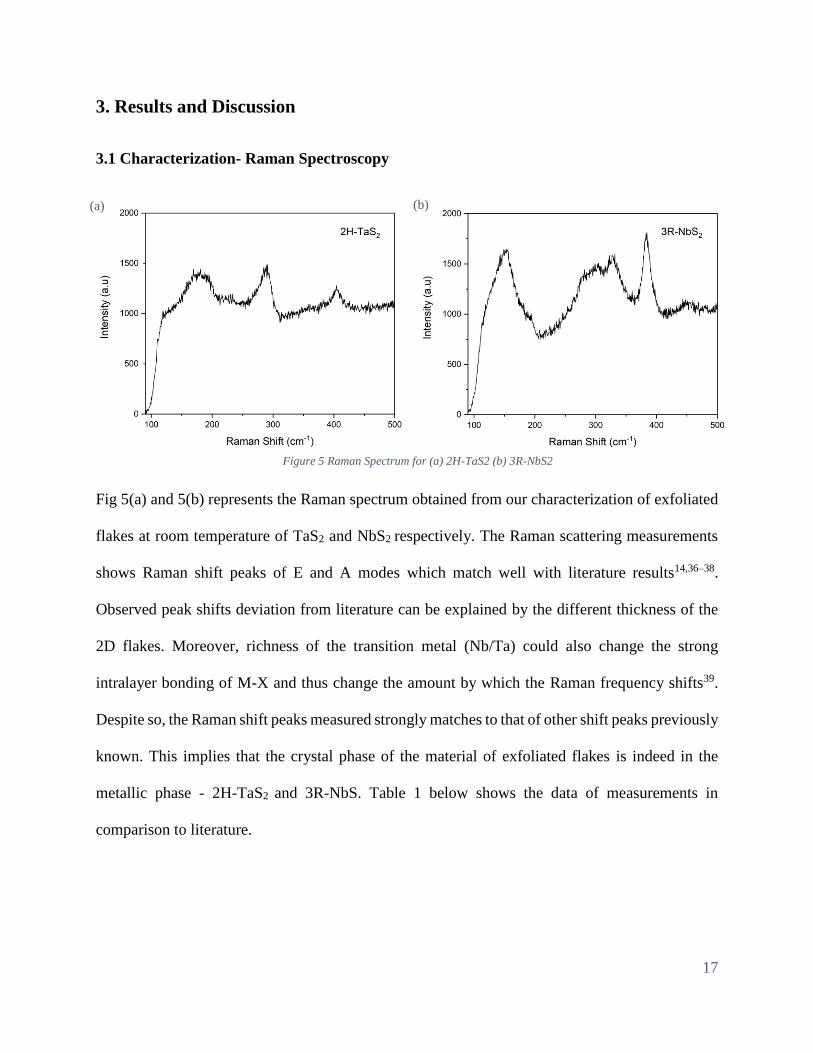
Fig 5(a) and 5(b) represents the Raman spectrum obtained from our characterization of exfoliated
flakes at room temperature of TaS2 and NbS2 respectively. The Raman scattering measurements
shows Raman shift peaks of E and A modes which match well with literature results14,36–38.
Observed peak shifts deviation from literature can be explained by the different thickness of the
2D flakes. Moreover, richness of the transition metal (Nb/Ta) could also change the strong
intralayer bonding of M-X and thus change the amount by which the Raman frequency shifts39.
Despite so, the Raman shift peaks measured strongly matches to that of other shift peaks previously
known. This implies that the crystal phase of the material of exfoliated flakes is indeed in the
metallic phase - 2H-TaS2 and 3R-NbS. Table 1 below shows the data of measurements in
comparison to literature.
(a)
(b)
Figure 5 Raman Spectrum for (a) 2H-TaS2 (b) 3R-NbS2
Figure 5 Raman Spectrum for (a) 2H-TaS2 (b) 3R-NbS2
Figure 5 Raman Spectrum for (a) 2H-TaS2 (b) 3R-NbS2
Figure 6 Raman Spectrum for (a) 2H-TaS2 (b) 3R-NbS2
18
Table 1 Comparison of observed Raman shift peak frequencies for exfoliated TaS2 and NbS2 against literature.
3.2 Characterization - AFM
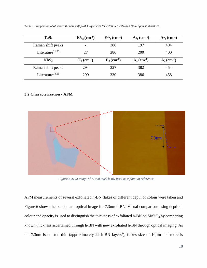
AFM measurements of several exfoliated h-BN flakes of different depth of colour were taken and
Figure 6 shows the benchmark optical image for 7.3nm h-BN. Visual comparison using depth of
colour and opacity is used to distinguish the thickness of exfoliated h-BN on Si/SiO2 by comparing
known thickness ascertained through h-BN with new exfoliated h-BN through optical imaging. As
the 7.3nm is not too thin (approximately 22 h-BN layers4), flakes size of 10µm and more is
TaS2 E12g (cm-1) E2
2g (cm-1) A1g (cm-1) A2g (cm-1)
Raman shift peaks - 288 197 404
Literature11,36 27 286 200 400
NbS2 E1 (cm-1) E2 (cm-1) A1 (cm-1) A2 (cm-1)
Raman shift peaks 294 327 382 454
Literature14,15 290 330 386 458
7.3nm
Figure 6 AFM image of 7.3nm thick h-BN used as a point of reference

19
relatively easy to look for under the optical microscope in 10x magnification. It is important to
note that any additional layer of h-BN changes the opacity and depth of colour of the optical image
of h-BN by a little and that would require a more detailed visual analysis and comparison to
distinguish. Moreover, during the screening for h-BN flakes to be used, the h-BN for use should
not have any form of uneven surface – which could be seen from very slight colour differences
under 100x magnification optical microscope, especially between overlapping areas of the
metal/insulator/metal flakes as this could undermine the intended tunnelling barrier width due to
current always flowing in the path of least resistance.
3.3 I-V Characteristics
The I-V characteristics of the MIM devices with FLG, TaS2 and NbS2 were measured, with results
given in Figure 7. Given the relatively large thickness (>5nm) of BN, the turn on voltage is on the
high bias side given that it shows a sharp exponential increase after the turn on voltage is reached.
Based on this fact, as well as from various studies, the current conduction mechanism for these
Figure 7 Current vs voltage, I-V characteristics of MIM structures
20
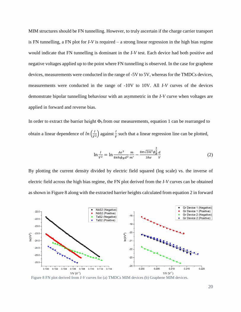
MIM structures should be FN tunnelling. However, to truly ascertain if the charge carrier transport
is FN tunnelling, a FN plot for I-V is required – a strong linear regression in the high bias regime
would indicate that FN tunnelling is dominant in the I-V test. Each device had both positive and
negative voltages applied up to the point where FN tunnelling is observed. In the case for graphene
devices, measurements were conducted in the range of -5V to 5V, whereas for the TMDCs devices,
measurements were conducted in the range of -10V to 10V. All I-V curves of the devices
demonstrate bipolar tunnelling behaviour with an asymmetric in the I-V curve when voltages are
applied in forward and reverse bias.
In order to extract the barrier height Φb from our measurements, equation 1 can be rearranged to
obtain a linear dependence of 𝑙𝑛 (𝐼
𝑉2) against 𝐼
𝑉 such that a linear regression line can be plotted,
ln𝐼
𝑉2 = ln𝐴𝑒3
8𝜋ℎ𝜙𝐵𝑑2
𝑚
𝑚∗ −8𝜋√2𝑚∗𝜙𝐵
32
3ℎ𝑒
𝑑
𝑉 (2)
By plotting the current density divided by electric field squared (log scale) vs. the inverse of
electric field across the high bias regime, the FN plot derived from the I-V curves can be obtained
as shown in Figure 8 along with the extracted barrier heights calculated from equation 2 in forward
Figure 8 FN plot derived from I-V curves for (a) TMDCs MIM devices (b) Graphene MIM devices.
21
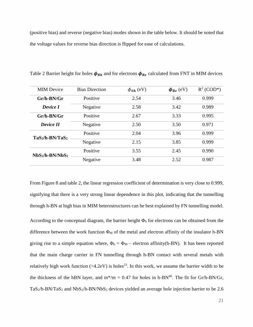
(positive bias) and reverse (negative bias) modes shown in the table below. It should be noted that
the voltage values for reverse bias direction is flipped for ease of calculations.
Table 2 Barrier height for holes 𝝓𝑩𝒉 and for electrons 𝝓𝑩𝒆 calculated from FNT in MIM devices
MIM Device Bias Direction 𝜙𝐵𝒉 (eV) 𝝓𝑩𝒆 (eV) R2 (COD*)
Gr/h-BN/Gr
Device I
Positive 2.54 3.46 0.999
Negative 2.58 3.42 0.989
Gr/h-BN/Gr
Device II
Positive 2.67 3.33 0.995
Negative 2.50 3.50 0.971
TaS2/h-BN/TaS2 Positive 2.04 3.96 0.999
Negative 2.15 3.85 0.999
NbS2/h-BN/NbS2 Positive 3.55 2.45 0.990
Negative 3.48 2.52 0.987
From Figure 8 and table 2, the linear regression coefficient of determination is very close to 0.999,
signifying that there is a very strong linear dependence in this plot, indicating that the tunnelling
through h-BN at high bias in MIM heterostructures can be best explained by FN tunnelling model.
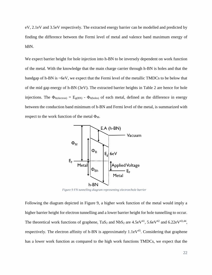
According to the conceptual diagram, the barrier height Φb for electrons can be obtained from the
difference between the work function ΦM of the metal and electron affinity of the insulator h-BN
giving rise to a simple equation where, Φb = ΦM – electron affinity(h-BN). It has been reported
that the main charge carrier in FN tunnelling through h-BN contact with several metals with
relatively high work function (>4.2eV) is holes23. In this work, we assume the barrier width to be
the thickness of the hBN layer, and m*/m = 0.47 for holes in h-BN40. The fit for Gr/h-BN/Gr,
TaS2/h-BN/TaS2 and NbS2/h-BN/NbS2 devices yielded an average hole injection barrier to be 2.6
22
eV, 2.1eV and 3.5eV respectively. The extracted energy barrier can be modelled and predicted by
finding the difference between the Fermi level of metal and valence band maximum energy of
hBN.
We expect barrier height for hole injection into h-BN to be inversely dependent on work function
of the metal. With the knowledge that the main charge carrier through h-BN is holes and that the
bandgap of h-BN is ~6eV, we expect that the Fermi level of the metallic TMDCs to be below that
of the mid gap energy of h-BN (3eV). The extracted barrier heights in Table 2 are hence for hole
injections. The Φb(electron) = Eg(BN) - Φb(holes) of each metal, defined as the difference in energy
between the conduction band minimum of h-BN and Fermi level of the metal, is summarized with
respect to the work function of the metal ΦM.
Following the diagram depicted in Figure 9, a higher work function of the metal would imply a
higher barrier height for electron tunnelling and a lower barrier height for hole tunnelling to occur.
The theoretical work functions of graphene, TaS2 and NbS2 are 4.5eV41, 5.6eV42 and 6.22eV43,44,
respectively. The electron affinity of h-BN is approximately 1.1eV45. Considering that graphene
has a lower work function as compared to the high work functions TMDCs, we expect that the
Figure 9 FN tunnelling diagram representing electron/hole barrier

23
hole injection barrier for the TMDCs MIM devices to be lower than that of the graphene device.
However, the calculations, when fitted to FN tunnelling parameters, were only conclusive for
graphene and TaS2 and not NbS2. Following the recent work of Hattori and Nagashio as described
previously, it can be seen that the average electron tunnelling barrier height 𝝓𝑩𝒆 for graphene and
TaS2 fits very well into their linear regression plot of barrier height against metal work function as
shown in Figure 10. However, for NbS2 which is a metallic TMDC with the highest work function
to display a barrier height that is opposite from the trend requires further study.
A second device of Au/h-BN/NbS2 using the Au electrode as the top layer and NbS2 as a second
layer, the FN plot shows a tunnelling barrier of 3.18eV in the forward bias and 3.44eV in the
negative bias which shows slightly better results as compared to the NbS2/h-BN/NbS2 device but
it is still not viable in the expected trend.
The possibility that there is significant oxygen penetration into NbS2 which may have altered the
device’s work function cannot be discounted. NbS2 is known to be an unstable TMDC in ambient
conditions. In fact, other groups has performed detailed transmission electron microscopy (TEM)
and energy-dispersive X-ray spectroscopy (EDS) analysis on NbS2 indicate that the NbS2 flakes
prepared in air oxidize during exfoliation, evidenced by the formation of 5-7 nm of niobium oxide
Figure 10 Visual fitting of graphene (Gr) and TaS2 into extrapolated known linear regression of barrier
height against work function
24
sandwiching the crystalline NbS2 layers46. Therefore, the transport properties in flakes below 5 nm
are significantly affected by NbOx, and the observed transport properties cannot be attributed as
intrinsic to NbS2. Despite working as fast as possible from the process of exfoliation to the
fabrication of the heterostructure, the formation of an oxide layer above our NbS2 flake is inevitable.
Plans to use NbS2 flakes of relatively large thickness (>30nm) to mitigate the effect the oxide layer
has proven to be ineffective too.
If we were to consider that there is an additional oxide layer sandwiching and supressing the NbS2
metallic properties, then the FN tunnelling through h-BN would have to consider two additional
layers of unknown Nb oxide. Not considering the charge transport through this oxide layer being
significantly different from that of h-BN, we can conclude that the tunnelling width would
significantly increase due to this oxide layer and hence making our calculations an overestimated
one based on standardizing the tunnelling width to only the h-BN.
Future plans towards reassessing the barrier height dependence on the work function of NbS2 can
include constructing a 5 layer heterostructure in a glove box where oxygen content is minimal and
formation of oxide layer can be slowed. A h-BN/NbS2/h-BN/NbS2/h-BN 5 layer heterostructure
can be constructed and the outer layers of h-BN can be used as encapsulation to protect device
from exposure to air when bringing it out of the glove box. This method would yield a more
accurate result that would allow us to really determine if NbS2 work function affects the barrier
height across h-BN is conclusive.
It is worth noting that there is asymmetry in MIM tunnelling device. It could be due to the different
thickness and surface quality of the two interfaces. It is known that graphene thickness, in the
range 1-5 layers, affects its effective work function47 which could be the cause for asymmetry in

25
our graphene devices. As our devices uses graphene that is approximately 2-5 layers thick, it is
certainly viable to say that asymmetry could be a result of the difference in thin layers thickness.
For the TMDCs heterostructures, the most likely cause would be the surface quality of the interface.
As NbS2 is not stable in ambient conditions, the likely cause would be the interactions between
the Nb oxide layer and h-BN layer that results in the asymmetry. Moreover, the fabrication process
is not contamination proof, residue from the polymer used for transfer could end up on the surface
of the flakes and during transfer some residue may be deposited on the interface of these devices.
These contaminations can actually be seen under dark field using the optical microscope. These
contaminations could be the cause for some undesired interface states that could potentially reduce
the current density through the device and hence affect our results.
26
4. Conclusion
In this work, we manifest the FN tunnelling characteristics of several MIM heterostructure devices
consisting of BN sandwiched by 2D metals (FLG, NbS2 and TaS2). We reason that the main charge
carrier is holes considering the band diagram of heterostructures along with I-V measurements of
these MIM devices that show that the barrier heights for holes depend on the work function of 2D
metals. The tunnelling barrier height for holes we extracted from the FN plot for TaS2 is smaller
than that of FLG, which is consistent with the expected band alignment. Barrier height extracted
for TaS2 and graphene is consistent with known trend of increasing work function. Despite so, the
results for NbS2 deviates significantly from prediction, which we attribute to possible oxidation of
the surface of the 2D metal. The present finding for hole injection for high work function metallic
TMDCs (up to 5.6eV) provides a valid understanding carrier tunneling and transport mechanism
in MIM 2D heterostructures.
27
References
1. Novoselov, K. S. et al. Electric field effect in atomically thin carbon films. Science 306, 666–9 (2004).
2. Geim, A. K. & Novoselov, K. S. The rise of graphene. Nat. Mater. 6, 183–191 (2007).
3. Xu, M., Liang, T., Shi, M. & Chen, H. Graphene-Like Two-Dimensional Materials. Chem. Rev. 113, 3766–
3798 (2013).
4. Golla, D. et al. Optical thickness determination of hexagonal boron nitride flakes. Appl. Phys. Lett. 102,
161906 (2013).
5. Stenger, I. et al. Low frequency Raman spectroscopy of few-atomic-layer thick hBN crystals. 2D Mater. 4,
031003 (2017).
6. Manzeli, S., Ovchinnikov, D., Pasquier, D., Yazyev, O. V. & Kis, A. 2D transition metal dichalcogenides.
Nat. Rev. Mater. 2, 17033 (2017).
7. Zhang, K., Feng, Y., Wang, F., Yang, Z. & Wang, J. Two dimensional hexagonal boron nitride (2D-hBN):
synthesis, properties and applications. J. Mater. Chem. C 5, 11992–12022 (2017).
8. Wang, J., Ma, F. & Sun, M. Graphene, hexagonal boron nitride, and their heterostructures: properties and
applications. (2017). doi:10.1039/c7ra00260b
9. Joshi, S. & Moddel, G. Efficiency limits of rectenna solar cells: Theory of broadband photon-assisted
tunneling. Appl. Phys. Lett. 102, 083901 (2013).
10. Iqbal, M. Z. & Faisal, M. M. Fowler-Nordheim tunneling characteristics of graphene/hBN/metal
heterojunctions. J. Appl. Phys. 125, 084902 (2019).
11. Navarro-Moratalla, E. et al. Enhanced superconductivity in atomically thin TaS2. Nat. Commun. 7, 11043
(2016).
12. Tsen, A. W. et al. Structure and Control of Charge Density Waves in Two-Dimensional 1T-TaS 2.
13. Grant, A. J., Griffiths, T. M., Yoffe, A. D. & Pitt, G. D. Pressure-induced semimetal-metal and metal-metal
28
transitions in 1T and 2H TaS 2. J. Phys. C Solid State Phys. 7, L249–L253 (1974).
14. McMullan, W. G. & Irwin, J. C. Raman scattering from 2H and 3R–NbS2. Solid State Commun. 45, 557–
560 (1983).
15. Ehm, L., Knorr, K. & Depmeier, W. The high-pressure behaviour of 3R-NbS2. Zeitschrift für Krist. - Cryst.
Mater. 217, 522–524 (2002).
16. Fowler, R. H. & Nordheim, L. Electron Emission in Intense Electric Fields. Proc. R. Soc. A Math. Phys.
Eng. Sci. 119, 173–181 (1928).
17. Monch, W. On the physics of metal-semiconductor interfaces. Reports Prog. Phys. 53, 221–278 (1990).
18. Mönch, W. Barrier Heights of Metal Contacts on H-Terminated Diamond: Explanation by Metal-Induced
Gap States and Interface Dipoles. Europhys. Lett. 27, 479–484 (1994).
19. Liu, Y., Stradins, P. & Wei, S.-H. Van der Waals metal-semiconductor junction: Weak Fermi level pinning
enables effective tuning of Schottky barrier. (2016). doi:10.1126/sciadv.1600069
20. Lee, G.-H. et al. Electron tunneling through atomically flat and ultrathin hexagonal boron nitride. Appl.
Phys. Lett. 99, 243114 (2011).
21. Ang, Y. S., Liang, S.-J. & Ang, L. K. Theoretical modeling of electron emission from graphene. MRS Bull.
42, 505–510 (2017).
22. Liang, S.-J., Hu, W., Bartolomeo, A. Di, Adam, S. & Ang, L. K. A modified Schottky model for graphene-
semiconductor (3D/2D) contact: A combined theoretical and experimental study.
23. Hattori, Y., Taniguchi, T., Watanabe, K. & Nagashio, K. Determination of Carrier Polarity in Fowler–
Nordheim Tunneling and Evidence of Fermi Level Pinning at the Hexagonal Boron Nitride/Metal Interface.
ACS Appl. Mater. Interfaces 10, 11732–11738 (2018).
24. Kim, C. et al. Fermi Level Pinning at Electrical Metal Contacts of Monolayer Molybdenum
Dichalcogenides. ACS Nano 11, 1588–1596 (2017).
25. Gong, C., Colombo, L., Wallace, R. M. & Cho, K. The Unusual Mechanism of Partial Fermi Level Pinning
29
at Metal–MoS 2 Interfaces. Nano Lett. 14, 1714–1720 (2014).
26. Vaziri, S. et al. A Graphene-Based Hot Electron Transistor. Nano Lett. 13, 1435–1439 (2013).
27. Wang, L. et al. One-dimensional electrical contact to a two-dimensional material. Science 342, 614–7
(2013).
28. Vaziri, S. et al. Bilayer insulator tunnel barriers for graphene-based vertical hot-electron transistors.
Nanoscale 7, 13096–13104 (2015).
29. Jayaswal, G. et al. Optical rectification through an Al2O3 based MIM passive rectenna at 28.3 THz. Mater.
Today Energy 7, 1–9 (2018).
30. Shin, J. H., Yang, J. H., Heo, S. J. & Jang, J. E. Geometric effect in a vertical stack-up metal-insulator-metal
tunnel diode. AIP Adv. 7, 105307 (2017).
31. Ding, L. et al. Understanding Interlayer Coupling in TMD-hBN Heterostructure by Raman Spectroscopy.
IEEE Trans. Electron Devices 65, 4059–4067 (2018).
32. Hu, Z. et al. Two-dimensional transition metal dichalcogenides: interface and defect engineering. Chem.
Soc. Rev. 47, 3100–3128 (2018).
33. Cong, C. et al. Synthesis and Optical Properties of Large-Area Single-Crystalline 2D Semiconductor WS 2
Monolayer from Chemical Vapor Deposition. Adv. Opt. Mater. 2, 131–136 (2014).
34. Ubaldini, A. & Giannini, E. Improved chemical vapor transport growth of transition metal dichalcogenides.
35. Pizzocchero, F. et al. The hot pick-up technique for batch assembly of van der Waals heterostructures. Nat.
Commun. 7, 11894 (2016).
36. Sugai, S., Murase, K., Uchida, S. & Tanaka, S. Studies of lattice dynamics in 2H-TaS2 by Raman scattering.
Solid State Commun. 40, 399–401 (1981).
37. Zhao, R. et al. Two-dimensional tantalum disulfide: controlling structure and properties via synthesis. 2D
Mater. 5, 025001 (2018).
38. Wang, D., Zhang, X. & Liu, H. Two-dimensional metallic NbS 2 : growth, optical identification and

30
transport properties Related content Epitaxial growth of HfS2 on sapphire by chemical vapor deposition and
application for photodetectors. (2016). doi:10.1088/2053-1583/3/2/025027
39. Dash, J. K., Chen, L., Dinolfo, P. H., Lu, T.-M. & Wang, G.-C. A Method Toward Fabricating
Semiconducting 3R-NbS 2 Ultrathin Films. (2015). doi:10.1021/acs.jpcc.5b04057
40. Xu, Y.-N. & Ching, W. Y. Calculation of ground-state and optical properties of boron nitrides in the
hexagonal, cubic, and wurtzite structures. Phys. Rev. B 44, 7787–7798 (1991).
41. Leenaerts, O., Partoens, B., Peeters, F. M., Volodin, A. & Van Haesendonck, C. The work function of few-
layer graphene. J. Phys. Condens. Matter 29, 035003 (2017).
42. Shimada, T., Ohuchi, F. S. & Parkinson, B. A. Work Function and Photothreshold of Layered Metal
Dichalcogenides. Jpn. J. Appl. Phys. 33, 2696–2698 (1994).
43. Terrones, H. & Terrones, M. Electronic and vibrational properties of defective transition metal
dichalcogenide Haeckelites: new 2D semi-metallic systems. 2D Mater. 1, 011003 (2014).
44. Farmanbar, M. & Brocks, G. Ohmic contacts to 2D semiconductors through van der Waals bonding.
45. Fiori, G., Betti, A., Bruzzone, S. & Iannaccone, G. Lateral Graphene–hBCN Heterostructures as a Platform
for Fully Two-Dimensional Transistors. ACS Nano 6, 2642–2648 (2012).
46. Yan, R. et al. Evolution of superconductivity in ultrathin NbS 2.
47. Ziegler, D. et al. Variations in the work function of doped single-and few-layer graphene assessed by Kelvin
probe force microscopy and density functional theory. Phys. Rev. B 83, 235434 (2011).
Related Documents


![Ch 12 [130 marks] · An electron of initial energy E tunnels through a potential barrier. What is the energy of the electron after tunnelling? A. greater than E ... The present activity](https://static.cupdf.com/doc/110x72/5e685b743fd00d32260a1b4a/ch-12-130-marks-an-electron-of-initial-energy-e-tunnels-through-a-potential-barrier.jpg)


![Schottky Barrier Heights Extraction of an Atomically Flat Ni ...Schottky-Barrier MOSFET Technology”, IEEE Transactions on Electron Devices, 53, p.1048-p.1058 (2006) [1.4] W. Mizubayashi,](https://static.cupdf.com/doc/110x72/60e94ab2f3e0e511165d0cec/schottky-barrier-heights-extraction-of-an-atomically-flat-ni-schottky-barrier.jpg)
![Ch. 12 Other quantum phenomena [141 marks] · An electron of initial energy E tunnels through a potential barrier. What is the energy of the electron after tunnelling? A. greater](https://static.cupdf.com/doc/110x72/5e685c6dd87ad05e4b5c2020/ch-12-other-quantum-phenomena-141-marks-an-electron-of-initial-energy-e-tunnels.jpg)