FILTER PELEWAT RENDAH TERKENDALI DIGITAL TUGAS AKHIR Diajukan untuk memenuhi salah satu syarat Memperoleh gelar Sarjana Teknik Program Studi Teknik Elektro i Disusun oleh: HADI SANJAYA NIM : 005114061 PROGRAM STUDI TEKNIK ELEKTRO JURUSAN TEKNIK ELEKTRO FAKULTAS SAINS DAN TEKNOLOGI UNIVERSITAS SANATA DHARMA YOGYAKARTA 2007

Welcome message from author
This document is posted to help you gain knowledge. Please leave a comment to let me know what you think about it! Share it to your friends and learn new things together.
Transcript

FILTER PELEWAT RENDAH TERKENDALI DIGITAL
TUGAS AKHIR
Diajukan untuk memenuhi salah satu syarat Memperoleh gelar Sarjana Teknik
Program Studi Teknik Elektro
i
Disusun oleh:
HADI SANJAYA
NIM : 005114061
PROGRAM STUDI TEKNIK ELEKTRO JURUSAN TEKNIK ELEKTRO
FAKULTAS SAINS DAN TEKNOLOGI UNIVERSITAS SANATA DHARMA
YOGYAKARTA 2007

DIGITALLY CONTROLLED LOW PASS FILTER
FINAL PROJECT
Presented as Partial Fulfillment of the Requirements
To Obtain the Sarjana Teknik Degree
In Electrical Engineering
ii
By : HADI SANJAYA
Student ID Number : 005114061
ELECTRICAL ENGINEERING STUDY PROGRAM ELECTRICAL ENGINEERING DEPARTMENT
SAINS AND TECHNOLOGY FACULTY SANATA DHARMA UNIVERSITY
YOGYAKARTA 2007
iii
iv

v

Katakanlah: “Dialah Allah adalah Yang Maha Esa”. Hanya Allah tempat bergantung. Dia tidak beranak dan tidak diperanakkan. Dan tidak ada satupun yang menyamai-Nya”.
(Al Ikhlash)
Karya ini kupersembahankan untuk :
Allah SWT dan junjungan Nabi Muhammad SAW (atas berkat dan rahmat-Nya)
Bapak Iswandi Umar & Ibu Sumarni yang selalu memberikan doa, kekuatan dan mendidikku
dengan penuh cinta, Kakakku Eko Susanto & Adik-
adikku Mira Tulistiana, Nery Indriana, terima kasih
atas dukungannya, Almamaterku
vi

vii
INTISARI
Filter pelewat rendah terkendali digital adalah filter pelewat rendah, dengan frekuensi penggal yang dapat dikendalikan secara digital dengan menggunakan masukan kode digital. Secara umum alat ini terdiri dari bagian digital dan bagian analog. Bagian digital terdiri dari pengendali masukan digital dan pengali, dan bagian analog terdiri dari filter pelewat rendah. Untuk pengendali masukan digital menggunakan 8 saklar dan untuk pengali menggunakan DAC 0832. Jadi frekuensi penggal pada filter ditala secara digital tergantung dari besarnya nilai dari masukan digital. Untuk filter digunakan filter jenis tapis peubah kondisi dengan tujuan agar saat frekuensi penggal diubah-ubah, faktor kualitasnya tetap. Proses perkalian antara masukan digital dengan komponen pengali ‘k’ dan tegangan referensi keluaran dari penguat beda pada rangkaian tapis peubah kondisi. Hasil perkalian merupakan masukan untuk rangkaian integrator pada rangkaian tapis peubah kondisi. Nilai masukan digital ditampilkan oleh LED dan frekuensi penggal diukur dengan menggunakan osiloskop. Pada tanggapan magnitude diperoleh laju kemiringan (roll-off) yang mempunyai kesalahan rata-rata sebesar 4,1 % dibandingkan dengan nilai teoritis, dan untuk pengukuraan frekuensi penggal didapatkan kesalahan rata-rata sebesar 2,36 % dibaningkan nilai teoritis.
kata kunci : filter pelewat rendah, masukan digital
viii
ABSTRACT
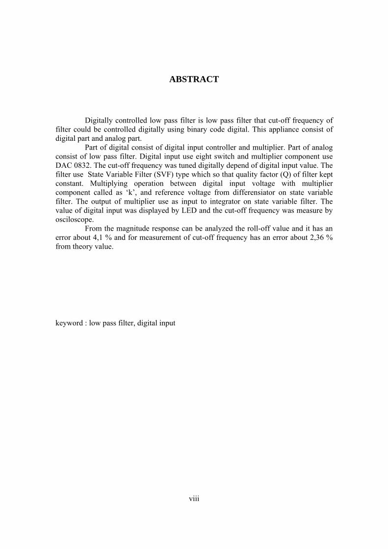
Digitally controlled low pass filter is low pass filter that cut-off frequency of filter could be controlled digitally using binary code digital. This appliance consist of digital part and analog part. Part of digital consist of digital input controller and multiplier. Part of analog consist of low pass filter. Digital input use eight switch and multiplier component use DAC 0832. The cut-off frequency was tuned digitally depend of digital input value. The filter use State Variable Filter (SVF) type which so that quality factor (Q) of filter kept constant. Multiplying operation between digital input voltage with multiplier component called as ‘k’, and reference voltage from differensiator on state variable filter. The output of multiplier use as input to integrator on state variable filter. The value of digital input was displayed by LED and the cut-off frequency was measure by osciloscope. From the magnitude response can be analyzed the roll-off value and it has an error about 4,1 % and for measurement of cut-off frequency has an error about 2,36 % from theory value. keyword : low pass filter, digital input
ix
KATA PENGANTAR
Dengan menyebut nama Allah yang Maha Pengasih lagi Maha Penyayang, oleh
karena petunjuk dan rahmat-Nya sehingga penulis dapat meyelesaikan Tugas Akhir
yang berjudul “Filter Pelewat Rendah Terkendali Digital”. Tugas Akhir ini disusun
sebagai salah satu syarat untuk memperoleh gelar Sarjana pada jurusan Teknik Elektro,
Fakultas Teknik Universitas Sanatha Dharma Yogyakarta.
Tersusunnya tugas akhir ini tidak terlepas dari bantuan dan dukungan dari berbagai
pihak. Pada kesempatan ini tidak lupa penulis mengucapkan terima kasih yang dalam
kepada :
1. Bapak Martanto, S.T., M.T., selaku Dosen Pembimbing I yang telah banyak
memberikan bimbingan dan pengarahan hingga tugas akhir ini dapat tersusun.
2. Bapak Ir. Tjendro, selaku dosen pembimbing II atas bimbingan dan bantuannya
sehingga penulis dapat menyelesaikan tugas akhir ini.
3. Bapak Djoko Untoro, S.Si., M.T., selaku Dosen Penguji yang telah memberikan
masukan dan saran.
4. Ibu Ir. Th. Prima Ari Setyani, M.T., selaku Dosen Penguji yang telah memberikan
masukan dan saran.
5. Bapak Iswandi Umar dan Ibunda Sumarni yang telah memberikan kasih dan
sayangnya, doa, dorongan, semangat, biaya yang tiada henti hingga terselesaikan
studi dan penyusunan tugas akhir ini.
6. Kakakku Eko Susanto dan Adik-adikku Mira Tulistiana, Nery Indriana atas
dukungan dan semangatnya.

x

xi
DAFTAR ISI
HALAMAN JUDUL ......................................................................................... .. i
HALAMAN PERSETUJUAN PEMBIMBING .............................................. .. iii
HALAMAN PENGESAHAN ........................................................................... .. iv
HALAMAN PERNYATAAN KEASLIAN KARYA ..................................... .. v
HALAMAN PERSEMBAHAN ........................................................................ .. vi
INTISARI ................. ......................................................................................... .. vii
ABSTRACT............... ......................................................................................... .. viii
KATA PENGANTAR ....................................................................................... .. ix
DAFTAR ISI ............ ......................................................................................... .. xi
DAFTAR TABEL .... ......................................................................................... .. xiv
DAFTAR GAMBAR ......................................................................................... .. xiv
DAFTAR LAMPIRAN ..................................................................................... .. xvi
BAB I PENDAHULUAN ......................................................................... .. 1
1.1 Judul ......................................................................................... .. 1
1.2 Latar Belakang.......................................................................... .. 1
1.3 Rumusan Masalah .................................................................... .. 2
1.4 Batasan Masalah....................................................................... .. 2
1.5 Tujuan dan Manfaat Penelitian................................................. .. 3
1.6 Metodologi Penelitian .............................................................. .. 3
1.7 Sistematika Penulisan............................................................... .. 4
xii
BAB II DASAR TEORI ............................................................................ .. 6
2.1 Filter ......................................................................................... .. 6
2.1.1 Definisi Filter................................................................ .. 6
2.1.2 Klasifikasi Filter ........................................................... .. 6
2.2 Penguat Operasional (Operasional Amplifier, Op-Amp) sebagai
pembangun dasar ..................................................................... .. 10
2.2.1 Dasar-Dasar Penguat Operasional ................................ .. 10
2.2.2 Penguat Membalik (Inverting Amplifier) ..................... .. 11
2.2.3 Penguat Tidak Membalik (Non Inverting Amplifier) ... .. 12
2.2.4 Pengikut Tegangan (Voltage Follower) ....................... .. 13
2.2.5 Penguat Penjumlah (Summing Amplifier) ................... .. 14
2.2.6 Integrator ...................................................................... .. 14
2.3 Filter Pelewat Rendah (Low Pass Filter, LPF) ........................ .. 16
2.4 Penapis Peubah Kondisi (State Variable Filter, SVF).. ........... .. 17
2.5 Digital to Analog Converter (DAC) ........................................ .. 21
2.5.2 DAC 0832.................................................................... .. 22
2.5.3 Akurasi dan Resolusi ................................................... .. 23
2.6 Pengali (Multiplier) ................................................................. .. 24
2.7 Saklar Mekanik......................................................................... .. 26
2.8 Saklar Transistor....................................................................... .. 27
BAB III RANCANGAN PENELITIAN .................................................... .. 30
3.1 Diagram Blok Filter Pelewat Rendah Terkendali Digital ........ .. 30

xiii
3.2 Buffer Analog............................................................................ .. 31
3.3 Filter Pelewat Rendah Terkendali Digital ................................ .. 31
3.4 Penampil LED .......................................................................... .. 35
3.5 Saklar Sebagai Kendali Masukan Digital................................. .. 38
BAB IV HASIL PENGAMATAN DAN PEMBAHASAN ...................... .. 40
4.1 Tanggapan Magnitude Sebagai Fungsi Frekuensi.................... .. 40
4.2 Penaksiran Nilai Roll-off pada Tanggapan Magnitude Sebagai
Fungsi Frekuensi ..................................................................... .. 55
4.3 Hubungan Antara Input Digital dengan Frekuensi cut-off....... .. 61
4.4 Hubungan Antara Tegangan Referensi dengan Tegangan
Keluaran Pengali ..................................................................... .. 65
BAB V KESIMPULAN DAN PENUTUP ............................................... .. 68
5.1 Kesimpulan ............................................................................. .. 68
5.2 Saran ……. ............................................................................. .. 68
DAFTAR PUSTAKA …….. ............................................................................ .. 70
LAMPIRAN

xiv
DAFTAR TABEL
Tabel 2.1 Masukan biner dan ekuivalen dalam desimal...................................... .. 22
Tabel 4.1 Konfigurasi saklar masukan digital saat pengamatan tanggapan
magnitude .. ......................................................................................... .. 41
Tabel 4.2 Tanggapan amplitudo relatif MdB (ω) pengamatan untuk urutan
rendah ....... ......................................................................................... .. 42
Tabel 4.3 Tanggapan amplitudo relatif MdB (ω) teoritis untuk urutan rendah... .. 44
Tabel 4.4 Tanggapan amplitudo relatif MdB (ω) pengamatan untuk urutan
sedang ........ ......................................................................................... .. 46
Tabel 4.5 Tanggapan amplitudo relatif MdB (ω) teoritis untuk urutan sedang .. .. 48
Tabel 4.6 Tanggapan amplitudo relatif MdB (ω) pengamatan untuk urutan
tinggi.......... ......................................................................................... .. 51
Tabel 4.7 Tanggapan amplitudo relatif MdB (ω) teoritis untuk urutan tinggi .... .. 53
Tabel 4.8. Penaksiran nilai roll-off pada tanggapan magnitude pengamatan...... .. 61

xv
DAFTAR GAMBAR
Gambar 2.1 Karakteristik ideal filter pelewat rendah ........................................... 8
Gambar 2.2 Karakteristik ideal filter pelewat tinggi ............................................. 8
Gambar 2.3 Karakteristik ideal filter pelewat jalur ............................................... 9
Gambar 2.4 Karakteristik ideal filter penolak jalur............................................... 9
Gambar 2.5 Simbol Op-Amp dalam rangkaian ..................................................... 10
Gambar 2.6 Comparator non inverting dengan bias positif .................................. 11
Gambar 2.7 Comparator inverting dengan bias positif ......................................... 11
Gambar 2.8 Rangkaian penguat inverting ............................................................. 11
Gambar 2.9 Rangkaian penguat non inverting ...................................................... 12
Gambar 2.10 Rangkaian pengikut tegangan............................................................ 13
Gambar 2.11 Rangkaian penguat penjumlah........................................................... 14
Gambar 2.12 Rangkaian integrator Op-Amp ........................................................... 14
Gambar 2.13 Rangkaian integrator yang menggunakan resistor untuk
meminimalkan offset error ................................................................ 15
Gambar 2.14 Tanggapan frekuensi Low Pass Filter Butterworth........................... 17
Gambar 2.15 Blok diagram filter pelewat rendah ................................................... 18
Gambar 2.16 Rangkaian filter pelewat rendah........................................................ 20
Gambar 2.17 Rangkaian ternormalisasi filter pelewat rendah ................................ 21
Gambar 2.18 Simbol DAC 0832 ............................................................................. 22
Gambar 2.19 Rangkaian R-2R Ladder pada DAC .................................................. 23
Gambar 2.20 Simbol pengali................................................................................... 24

xvi
Gambar 2.21 DAC yang dihubungkan ke sebuah Op-Amp.................................... 25
Gambar 2.22 Rangkaian pengali menggunakan DAC ............................................ 26
Gambar 2.23 Rangkaian saklar mekanik................................................................. 27
Gambar 2.24 Rangkaian saklar transistor................................................................ 27
Gambar 2.25 Karakteristik keluaran transistor........................................................ 28
Gambar 2.26 Transistor sebagai saklar tertutup...................................................... 29
Gambar 2.27 Transistor sebagai saklar terbuka ...................................................... 29
Gambar 3.1 Diagram blok filter pelewat rendah terkendali digital....................... 30
Gambar 3.2 Rangkaian pengikut tegangan menggunakan IC LF347.................... 31
Gambar 3.3 Diagram blok yang mempresentasikan persamaan (3.6)................... 32
Gambar 3.4 Rangkaian filter pelewat rendah dengan pengali menggunakan
DAC................................................................................................... 34
Gambar 3.5 Rangkaian saklar transistor untuk menyalakan LED ........................ 35
Gambar 3.6 Gambar rangkaian penampil LED..................................................... 38
Gambar 3.7 Rangkaian saklar masukan digital ..................................................... 38
Gambar 3.8 Rangkaian 8 saklar masukan digital................................................... 39
Gambar 4.1. Tanggapan magnitude hasil pengamatan dari urutan 1 sampai
urutan 3.............................................................................................. 44
Gambar 4.2 Tanggapan magnitude secara teoritis dari urutan ke 1 sampai urutan
ke 3 .................................................................................................... 46
Gambar 4.3 Tanggapan magnitude hasil pengamatan untuk dari urutan ke 100
sampai urutan ke 102....................................................................... 48
Gambar 4.4 Tanggapan magnitude secara teoritis dari urutan ke 101 sampai

xvii
urutan ke 102 ..................................................................................... 50
Gambar 4.5 Tanggapan magnitude hasil pengamatan untuk dari urutan ke 253
sampai urutan ke 255......................................................................... 53
Gambar 4.6 Tanggapan magnitude secara teoritis dari urutan ke 253 sampai
urutan ke 255 ..................................................................................... 55
Gambar 4.7 Nilai roll-off tanggapan magnitude untuk urutan ke 1 ...................... 58
Gambar 4.8 Nilai roll-off tanggapan magnitude untuk urutan ke 2 ...................... 58
Gambar 4.9 Nilai roll-off tanggapan magnitude untuk urutan ke 3 ..................... 59
Gambar 4.10 Nilai roll-off tanggapan magnitude untuk urutan ke 100 .................. 59
Gambar 4.11 Nilai roll-off tanggapan magnitude untuk urutan ke 101 .................. 60
Gambar 4.12 Nilai roll-off tanggapan magnitude untuk urutan ke 102 .................. 60
Gambar 4.13 Nilai roll-off tanggapan magnitude untuk urutan ke 253 .................. 61
Gambar 4.14 Nilai roll-off tanggapan magnitude untuk urutan ke 254 .................. 61
Gambar 4.15 Nilai roll-off tanggapan magnitude untuk urutan ke 255 .................. 62
Gambar 4.16 Grafik hubungan antara masukan digital dengan frekuensi cut-off
berdasarkan pengamatan dan teori .................................................... 64
Gambar 4.17 Grafik hubungan antara masukan digital dengan galat untuk
frekuensi cut-off ................................................................................. 65
Gambar 4.18 Grafik hubungan antara masukan digital dengan tegangan referensi
dan keluaran pengali.......................................................................... 67
Gambar 4.19 Grafik hubungan antara masukan digital dengan galat untuk tegangan
keluaran pengali................................................................................. 68

xviii
DAFTAR LAMPIRAN
Tabel hubungan input digital dengan frekuensi cut-off ............................................. A
Tabel hubungan input digital dengan tegangan referensi dan tegangan output
pengali............. ........................................................................................................ B
Gambar rangkaian keseluruhan ................................................................................. C
Gambar rangkaian catu daya ..................................................................................... D
Datasheet ................................................................................................................... E

1
BAB I
PENDAHULUAN
1.1. Latar Belakang Masalah
Kemajuan ilmu pengetahuan dan teknologi pada saat ini telah
mempengaruhi segala bidang kehidupan manusia, termasuk dalam bidang
elektronika. Salah satu pengaruh yang ditimbulkan adalah adanya pengembangan
suatu sistem pengendalian, yaitu yang semula dilakukan secara analog kini telah
mulai dialihkan secara digital. Pengembangan tersebut dimaksudkan agar
pekerjaan yang dilakukan menjadi lebih praktis. Dalam hal ini, pengembangan
dilakukan atas suatu sistem yang lama atau hanya mengubah beberapa bagian
kecil saja.
Sistem pengendalian secara digital sebenarnya tidak jauh berbeda dengan
sistem pengendalian secara analog. Namun jika dilihat dari segi kepraktisan,
sistem pengendalian secara digital lebih praktis sebab hanya memasukkan bit-bit
data secara langsung atau tidak langsung melalui saklar yang sudah tersedia.
Dalam sistem komunikasi, filter mempunyai kegunaan yang sangat besar
sebab bertugas untuk melewatkan sinyal dengan frekuensi yang dikehendaki dan
melemahkan sinyal dengan frekuensi yang tidak diinginkan. Berdasarkan hal
tersebut, telah banyak peralatan elektronik pendukung sistem komunikasi yang
digunakan oleh manusia, seperti telefon, radio, maupun televisi, menggunakan
filter sebagai salah satu komponen. Pada penelitian ini akan dibahas mengenai
salah satu jenis filter, yaitu Filter Pelewat Rendah (Low Pass Filter, LPF) yang

2
dikendalikan secara digital sehingga diperoleh frekuensi cut-off yang dapat
diubah-ubah. Pengendalian dilakukan dengan cara menambahkan pengali
(multiplier) di dalam filter yang bekerja berdasarkan kondisi masukan digital dari
8 saklar.
1.2. Rumusan Masalah
Rumusan masalah yang dihadapi adalah bagaimana merancang Filter
Pelewat Rendah menggunakan modul integrator, agar dapat diketahui posisi
pengali sebagai pengendali frekuensi cut-off. Bagaimana mengubah-ubah
frekuensi cut-off dari konfigurasi yang telah diperoleh sehingga perubahan
frekuensi tiap bit mempunyai step yang tetap dari batas minimum sampai batas
maksimum.
1.3. Batasan Masalah
Pada penelitian ini, dilakukan batasan-batasan terhadap sistem yang akan
diteliti. Batasan yang dilakukan antara lain :
1. Dalam realisasi digunakan Penapis Peubah Kondisi (State Variable
Filter, SVF) yang berbasis pada Butterworth orde 2 serta frekuensi
yang diubah-ubah hanya frekuensi cut-off dari Low Pass Filter.
2. Step kenaikan frekuensi ditentukan sebesar 100 Hz, dimulai dari
frekuensi 100 Hz.
3. Berbasis Butterworth orde 2 (faktor kualitas (Q) sebesar 0,707).
4. Penguatan tegangan sebesar 1.

3
5. Pengendalian frekuensi cut-off menggunakan Digital to Analog
Converter 8 bit.
6. Untuk penunjang yang lain digunakan saklar sebagai masukan
digital dan buffer analog.
7. Pengujian sistem dibatasi pada tanggapan frekuensi yang sekaligus
menyatakan tanggapan magnitude, sedangkan tanggapan fase tidak
diperhatikan.
1.4. Tujuan dan Manfaat Penelitian
Tujuan yang ingin dicapai adalah dapat merancang dan membuat Filter
Pelewat Rendah menggunakan rangkaian State Variable Filter yang dikendalikan
secara digital.
Beberapa manfaat yang diharapkan dapat diperoleh dari penelitian ini
adalah sebagai berikut :
1. Tersedianya Filter Pelewat Rendah untuk menghasilkan frekuensi
cut-off yang dapat diubah-ubah.
2. Sistem pengendalian yang dilakukan secara praktis.
3. Sebagai dasar pengembangan untuk aplikasi yang lebih bervariasi.
4. Sebagai referensi yang dapat mendukung penelitian selanjutnya
yang berkaitan dengan Filter Pelewat Rendah.

4
1.5. Metodologi Penelitian
Dalam penyusunan Tugas Akhir ini dilakukan beberapa metodologi
penelitian. Adapun metodologi penelitian yang dilakukan terdiri dari :
1. Studi Pustaka, yaitu dengan mengumpulkan dan mempelajari
berbagai informasi, baik dari buku, makalah maupun internet
mengenai hal-hal yang berkaitan dengan Filter Pelewat Rendah,
sehingga informasi yang diperoleh dapat digunakan sebagai
referensi pendukung dalam penyusunan laporan.
2. Merealisasikan pengetahuan yang diperoleh dalam bentuk
perancangan hardware.
3. Melakukan pengujian terhadap hasil perancangan agar dapat
diketahui hasil secara realistis.
4. Menganalisis hasil pengujian dan membandingkan dengan teori
yang ada.
5. Mengambil kesimpulan terhadap perancangan dan pengujian yang
telah dilakukan.
6.
1.6. Sistematika Penulisan
Sistematika penulisan Tugas Akhir ini terbagi menjadi 5 bab yang disusun
sebagai berikut :
BAB I. PENDAHULUAN

5
Bab ini berisi tentang latar belakang masalah, rumusan masalah,
batasan masalah, tujuan dan manfaat penelitian, metodologi penelitian
serta sistematika penulisan.
BAB II. DASAR TEORI
Bab ini berisi penjelasan-penjelasan umum serta persamaan
matematis yang berkaitan dengan filter pelewat rendah terkendali
digital.
BAB III. RANCANGAN PENELITIAN
Bab ini berisi tentang rancangan filter pelewat rendah terkendali
sigital, yang meliputi diagram blok, penjelasan cara kerja secara
singkat dan pemilihan komponen.
BAB IV. HASIL PENGAMATAN DAN PEMBAHASAN
Bab ini hasil dari penelitian dan pembahasan dari pengujian yang
telah dilakukan.
BAB V. PENUTUP
Bab ini tentang kesimpulan dan saran.

6
BAB II
DASAR TEORI
2.1. Filter
2.1.1. Definisi Filter
Filter didefinisikan sebagai sebuah alat atau rangkaian atau substansi
yang meneruskan atau meloloskan arus listrik pada frekuensi-frekuensi atau
jangkauan frekuensi tertentu serta menahan (menghalangi) frekuensi-frekuensi
lainnya.
2.1.2. Klasifikasi Filter
Berdasarkan komponen pendukung, filter dapat diklasifikasikan
menjadi 2 macam, yaitu : filter pasif dan filter aktif.
1. Filter Pasif
Filter pasif merupakan rangkaian filter yang hanya terdiri dari inti
filter, yaitu kombinasi resistor (R), kapasitor (C), dan induktor (L).
Kelebihan yang dimiliki yaitu : mampu memenuhi karakteristik filter yang
bagus dengan penerapan yang luas dari frekuensi audio sampai frekuensi
yang sangat tinggi, serta handal pada penerapan frekuensi yang sangat
tinggi. Sedangkan kekurangannya, yaitu : adanya masalah pada sisi
frekuensi rendah pada rentang frekuensi audio, ukuran fisik induktor yang
semakin besar untuk induktansi yang besar dan biaya untuk pengadaan
induktor yang relatif cukup besar.
7
2. Filter aktif
Filter aktif merupakan suatu rangkaian filter yang terdiri dari
kombinasi resistor, kapasitor dan satu atau lebih komponen aktif, biasanya
penguat operasional dengan feedback. Kelebihan yang dimiliki yaitu :
penguat operasional mampu menyediakan penguatan atau gain. Sinyal
masukan tidak akan mengalami pelemahan (atenuasi) selama sinyal-sinyal
dengan frekuensi-frekuensi yang dikehendaki dilewatkan oleh filter. Biaya
pembuatan filter murah sebab tidak menggunakan komponen induktor yang
harganya relatif mahal dan tidak selalu tersedia di pasaran, mudah diatur
(tune) untuk jangkauan frekuensi yang lebar tanpa mempengaruhi tanggapan
rangkaian yang telah ditentukan (sesuai dengan yang diinginkan), serta
memiliki impedansi masukan yang tinggi dan keluaran yang rendah akibat
dari penggunaan penguat operasional yang juga hampir menjamin tidak
adanya interaksi antara filter dengan sumber atau beban sinyal. Sedangkan
kekuranganya, yaitu : membutuhkan catu daya sendiri, kurang handal
dibandingkan komponen pasif, perlu feedback sehingga ada kemungkinan
tidak stabil dan batasan frekuensi kerja 100 KHz (bekerja baik dibawah
frekuensi 100 KHz).
Berdasarkan jangkauan frekuensi yang dilewatkan (passband) dan jangkauan
frekuensi yang ditolak (stop band), filter dapat diklasifikasikan menjadi 4
macam, yaitu : Filter Pelewat Rendah (Low Pass Filter, LPF), Filter Pelewat
Tinggi (High Pass Filter, HPF), Filter Pelewat Jalur(Band Pass Filter, BPF) dan
Filter Penolak Jalur (Band Rejected Filter, BRF).

8
1. Filter Pelewat Rendah
Filter pelewat rendah memilih frekuensi-frekuensi rendah dan menolak
frekuensi-frekuensi tinggi. Karakteristik ideal filter pelewat rendah ditunjukkan
oleh gambar 2.1.
Gambar 2.1. Karakteristik ideal filter pelewat rendah
2. Filter Pelewat Tinggi
Filter pelewat tinggi menolak frekuensi-frekuensi rendah dan
melewatkan frekuensi tinggi. Karakteristik ideal filter pelewat tinggi ditunjukkan
oleh gambar 2.2.
Gambar 2.2. Karakteristik ideal filter pelewat tinggi
3. Filter Pelewat Jalur
Filter pelewat jalur melewatkan frekuensi-frekuensi dalam pita
tertentu, sedangkan frekuensi-frekuensi diatas pita semuanya ditolak.
Karakteristik ideal filter pelewat jalur ditunjukkan oleh gambar 2.3.
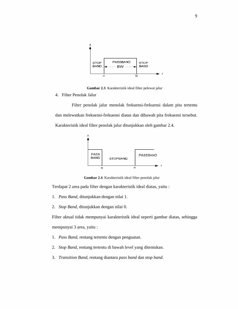
9
Gambar 2.3. Karakteristik ideal filter pelewat jalur
4. Filter Penolak Jalur
Filter penolak jalur menolak frekuensi-frekuensi dalam pita tertentu
dan melewatkan frekuensi-frekuensi diatas dan dibawah pita frekuensi tersebut.
Karakteristik ideal filter penolak jalur ditunjukkan oleh gambar 2.4.
Gambar 2.4. Karakteristik ideal filter penolak jalur
Terdapat 2 area pada filter dengan karakteristik ideal diatas, yaitu :
1. Pass Band, ditunjukkan dengan nilai 1.
2. Stop Band, ditunjukkan dengan nilai 0.
Filter aktual tidak mempunyai karakteristik ideal seperti gambar diatas, sehingga
mempunyai 3 area, yaitu :
1. Pass Band, rentang tertentu dengan penguatan.
2. Stop Band, rentang tertentu di bawah level yang ditentukan.
3. Transition Band, rentang diantara pass band dan stop band.
10
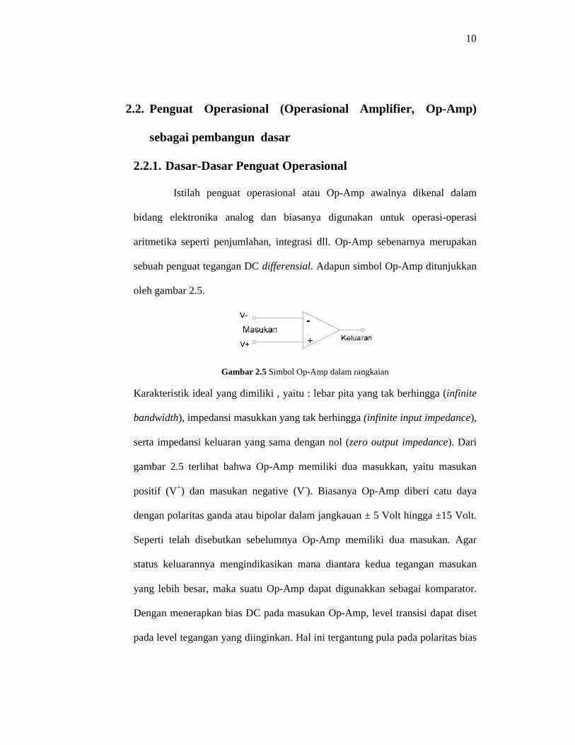
2.2. Penguat Operasional (Operasional Amplifier, Op-Amp)
sebagai pembangun dasar
2.2.1. Dasar-Dasar Penguat Operasional
Istilah penguat operasional atau Op-Amp awalnya dikenal dalam
bidang elektronika analog dan biasanya digunakan untuk operasi-operasi
aritmetika seperti penjumlahan, integrasi dll. Op-Amp sebenarnya merupakan
sebuah penguat tegangan DC differensial. Adapun simbol Op-Amp ditunjukkan
oleh gambar 2.5.
Gambar 2.5 Simbol Op-Amp dalam rangkaian
Karakteristik ideal yang dimiliki , yaitu : lebar pita yang tak berhingga (infinite
bandwidth), impedansi masukkan yang tak berhingga (infinite input impedance),
serta impedansi keluaran yang sama dengan nol (zero output impedance). Dari
gambar 2.5 terlihat bahwa Op-Amp memiliki dua masukkan, yaitu masukan
positif (V+) dan masukan negative (V-). Biasanya Op-Amp diberi catu daya
dengan polaritas ganda atau bipolar dalam jangkauan ± 5 Volt hingga ±15 Volt.
Seperti telah disebutkan sebelumnya Op-Amp memiliki dua masukan. Agar
status keluarannya mengindikasikan mana diantara kedua tegangan masukan
yang lebih besar, maka suatu Op-Amp dapat digunakkan sebagai komparator.
Dengan menerapkan bias DC pada masukan Op-Amp, level transisi dapat diset
pada level tegangan yang diinginkan. Hal ini tergantung pula pada polaritas bias

11
dan pada terminal Op-Amp mana yang diberi bias. Comparator non inverting
dengan bias positif ditunjukkan oleh gambar 2.6.
Gambar 2.6. Comparator non inverting dengan bias positif
Comparator inverting dengan bias positif ditunjukkan oleh gambar 2.7.
Gambar 2.7 Comparator inverting dengan bias positif
Selanjutnya pada pembahasan-pembahasan berikutnya rangkaian Op-Amp yang
digunakan dalam filter aktif selalu berbentuk atau menggunakan umpan balik
eksternal yang berguna untuk menstabilkan karakteristik Op-Amp itu sendiri.
2.2.2. Penguat Membalik (Inverting Amplifier)
Rangkaian penguat inverting ditunjukkan pada gambar 2.8.
Gambar 2.8 Rangkaian penguat inverting
Keterangan : Ra = Hambatan masukan, Rb = Hambatan umpan balik
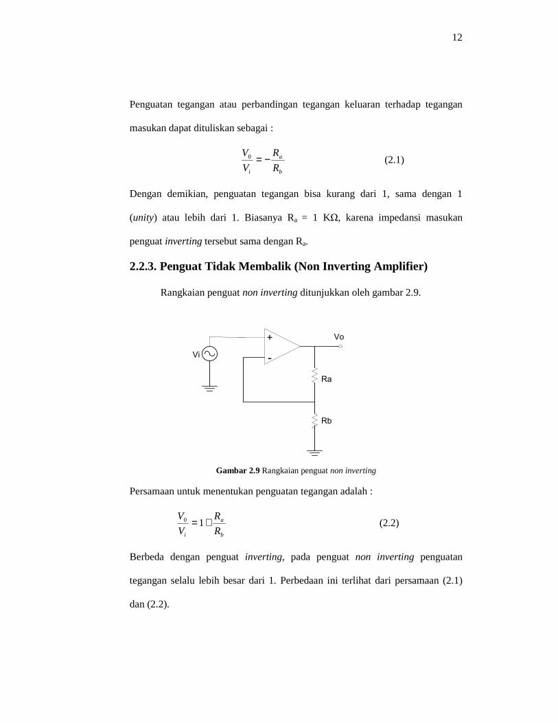
12
Penguatan tegangan atau perbandingan tegangan keluaran terhadap tegangan
masukan dapat dituliskan sebagai :
b
a
i R
R
V
V−=0 (2.1)
Dengan demikian, penguatan tegangan bisa kurang dari 1, sama dengan 1
(unity) atau lebih dari 1. Biasanya Ra = 1 KΩ, karena impedansi masukan
penguat inverting tersebut sama dengan Ra.
2.2.3. Penguat Tidak Membalik (Non Inverting Amplifier)
Rangkaian penguat non inverting ditunjukkan oleh gambar 2.9.
Gambar 2.9 Rangkaian penguat non inverting
Persamaan untuk menentukan penguatan tegangan adalah :
b
a
i R
R
V
V+= 10 (2.2)
Berbeda dengan penguat inverting, pada penguat non inverting penguatan
tegangan selalu lebih besar dari 1. Perbedaan ini terlihat dari persamaan (2.1)
dan (2.2).
-
+ Vo
Ra
Vi
Rb

13
2.2.4. Pengikut Tegangan (Voltage Follower)
Pengikut tegangan kadang-kadang disebut penyangga atau buffer dan
memiliki fungsi yang sama dengan pengikut emitter (emitter follower). Ciri-ciri
yang dimiliki, yaitu : impedansi masukan sangat tinggi (lebih dari 100 KΩ) dan
impedansi keluaran yang sangat rendah (kurang dai 75Ω).
Gambar 2.10 menunjukkan rangkaian pengikut tegangan.
Gambar 2.10 Rangkaian pengikut tegangan
Jika dibandingkan dengan rangkaian penguat non inverting, pada rangkaian
pengikut tegangan, Ra = ∞ dan Rb = 0. Dengan demikian penguatan tegangan
selalu 1.
10 =iV
V (2.3)
Sehingga dapat diketahui bahwa sinyal keluaran sama persis (identik) dengan
sinyal masukan. Fungsi utama dari dari rangkaian ini adalah sebagai penyangga
atau mengisolasi beban dari sumber.
2.2.5. Penguat Penjumlah (Summing Amplifier)
Rangkaian penguat penjumlah dapat menjumlahkan dua atau lebih
masukan-masukan bebas. Gambar 2.11 menunjukkan rangkaian untuk penguat
penjumlah.
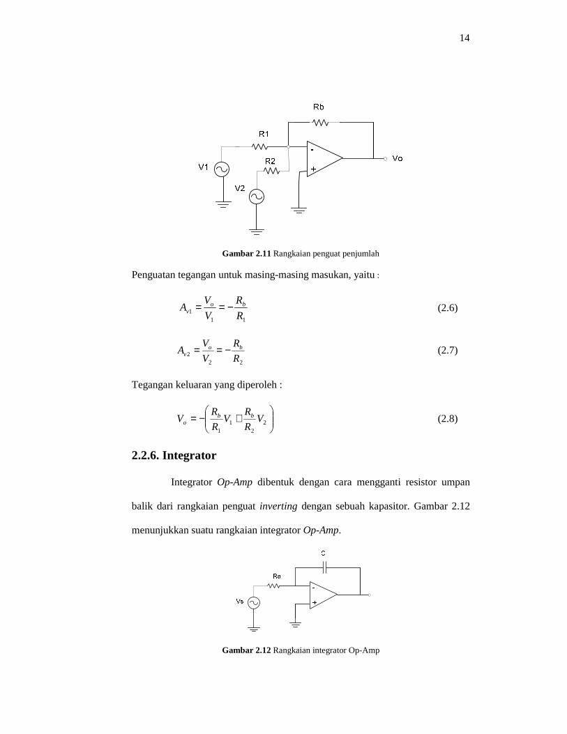
14
Gambar 2.11 Rangkaian penguat penjumlah
Penguatan tegangan untuk masing-masing masukan, yaitu :
11
1 R
R
V
VA bo
v −== (2.6)
22
2 R
R
V
VA bo
v −== (2.7)
Tegangan keluaran yang diperoleh :
+−= 2
21
1
VR
RV
R
RV bb
o (2.8)
2.2.6. Integrator
Integrator Op-Amp dibentuk dengan cara mengganti resistor umpan
balik dari rangkaian penguat inverting dengan sebuah kapasitor. Gambar 2.12
menunjukkan suatu rangkaian integrator Op-Amp.
Gambar 2.12 Rangkaian integrator Op-Amp

15
Berdasarkan gambar diatas, sinyal masukan diintegralkan dan sekaligus
menyatakan “luasan dibawah kurva”. Tegangan keluaran yang dihasilkan,
yaitu :
∫−= dtVCR
V sa
o
1 (2.9)
BentukCRa
1 harus sesuai dengan masukan frekuensi minimum yang
diharapkan :
min2
1
fCRa π
= (2.10)
Karena integrator juga bereaksi terhadap sembarang tegangan offset resultant
keluaran (berkaitan dengan offset arus bias Op-Amp), sebuah resistor (Ra )
sering diletakkan diantara masukan positif dengan ground untuk meminimalkan
offset ini. Gambar 2.13 menunjukkan rangkaian integrator yang menggunakan
resistor untuk meminimalkan offset error.
Gambar 2.13 Rangkaian integrator yang menggunakan resistor untuk meminimalkan offset
error
Efek offset dapat melibatkan tegangan maupun arus, dan dapat terjadi secara
internal maupun eksternal terhadap Op-Amp itu sendiri. Suatu arus atau

16
tegangan offset dapat menyebabkan tegangan keluaran tidak nol untuk tegangan
masukan yang nol. Biasanya, Op-Amp itu sendiri memiliki offset yang telah
disesuaikan hingga beberapa milivolt mengacu pada masukan. Offset terjadi
pada saat arus bias masukan mengakibatkan penurunan tegangan yang melalui
hambatan masukan. Jika penurunan tegangan terjadi pada masukan (+) dan (-)
dapat dibuat sama atau identik, maka offset tersebut dapat dihilangkan.
2.3. Filter Pelewat Rendah (Low Pass Filter, LPF)
Seperti telah dijelaskan sebelumnya, LPF melewatkan frekuensi-
frekuensi rendah dan menolak frekuensi-frekuensi tinggi. Adapun fungsi alih dari
(transfer function) untuk LPF orde 2 Butterworth standar ditunjukkan oleh
persamaan berikut :
2
002
200
ωωω
++=
sQ
s
AH lp (2.11)
dengan :
ωo = frekuensi cut-off LPF
Ao = penguatan tegangan
Q = faktor kualitas
Faktor kualitas pada LPF Butterworth orde 2 adalah 0,707. Sedangkan
fungsi alih dalam keadaan tunak (steady state), H(jω) untuk LPF orde 2 dapat
dinyatakan sebagai :
nfcf
M2)/(1
1)(
+=ω (2.12)
17
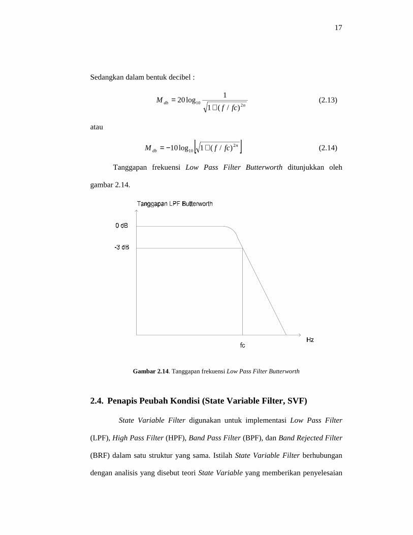
Sedangkan dalam bentuk decibel :
ndb
fcfM
210)/(1
1log20
+= (2.13)
atau
[ ]ndb fcfM 2
10 )/(1log10 +−= (2.14)
Tanggapan frekuensi Low Pass Filter Butterworth ditunjukkan oleh
gambar 2.14.
Gambar 2.14. Tanggapan frekuensi Low Pass Filter Butterworth
2.4. Penapis Peubah Kondisi (State Variable Filter, SVF)
State Variable Filter digunakan untuk implementasi Low Pass Filter
(LPF), High Pass Filter (HPF), Band Pass Filter (BPF), dan Band Rejected Filter
(BRF) dalam satu struktur yang sama. Istilah State Variable Filter berhubungan
dengan analisis yang disebut teori State Variable yang memberikan penyelesaian

18
sistematis suatu persamaan differensial dari sistem yang besar. Secara teoritis,
dapat dirancang SVF orde berapapun, tapi kebanyakan perancangan berbasis pada
orde 2. Perancangan dengan orde 2 lebih tahan terhadap variasi parameter
dibandingkan dengan perancangan menggunakan orde lebih tinggi. Orde yang
lebih tinggi dibuat dengan mengkaskade orde-orde berbasis 2, sedangkan untuk
perancangan dengan orde ganjil diperlukan filter dengan orde ganjil.
Untuk mengimplementasikan filter pelewat jalur dalam bentuk SVF,
digunakan persaman fungsi alih filter pelewat rendah orde 2 standar, yaitu seperti
diperlihatkan pada persamaan (2.11). Persamaan tersebut dapat diubah menjadi
sebagai berikut :
2
002
200
ωωω
++=
sQ
s
A
V
V
i
lp (2.15)
Dari persamaan (2.19), dilakukan sintesis sehingga menjadi rangkaian yang
dibentuk dari rangkaian modul integrator. Ada 3 tahapan matematis dasar yang
diperlukan untuk mengimplementasikan persamaan fungsi alih ini, yaitu :
• Perkalian silang (cross multiplying), yaitu perkalian antara sinyal keluaran
dengan penyebut dan antara sinyal masukan sengan pembilang dari fungsi
alih filter pelewat rendah.
• Melakukan pembagian hasil tahap pertama dengan variabel s yang memiliki
pangkat terbesar.
• Menyusun kembali persamaan hasil tahap kedua untuk mendapatkan
pernyataan sinyal keluaran.
Dengan melakukan ketiga tahapan diatas, persamaan (2.19) menjadi :

19
( )222ooio
olp AVs
QsV ωωω
=
++ (2.16)
=
++
2
20
2
2001
sAV
ssQV oilp
ωωω (2.17)
2
00
2
0 1
−
−
=s
VsQ
Vs
AVV lplpoilp
ωωω (2.18)
−−+
−
−=s
VVQs
AVs
V lplpoilp000 1 ωωω
(2.19)
[ ]
+−
−
−= lplpoilp VQ
VAVss
V100 ωω
(2.20)
Persamaan (2.24) menyatakan persamaan untuk sebuah jaringan dengan
menggunakan modul integrator, komponen (ωo/s) menunjukkan suatu modul
integrator dalam filter. Untuk memperoleh realisasi yang paling sederhana,
persamaan (2.24) dapat disusun menjadi :
[ ]
−−
−−
−= lpoilplp VQ
AVVss
V100 ωω
(2.21)
Diagram blok yang mempresentasikan persamaan (2.21) ditunjukkan pada gambar
2.15.
soω
−s
oω−
Q
1
ΣΣoA
Gambar 2.15. Blok diagram filter pelewat rendah

20
Jika gambar 2.16 dihubungkan ke modul integrator dan penguat beda, maka
rangkaian filter pelewat rendah ditunjukkan oleh gambar 2.16.
Gambar 2.16 Rangkaian filter pelewat rendah
Karena ini adalah LPF Butterworth orde 2, maka faktor kualitas untuk LPF ini
adalah sebesar 0,707 yang didapat dari 1/α, dimana α adalah faktor redaman
untuk Low Pass Filter Butterworth sebesar 1,414.
Jika dilihat dari rangkaian filter pelewat rendah pada gambar 2.17, maka
dapat diperoleh faktor penguatan filter pelewat rendah dari feedback Vlp menuju
masukan non inverting penguat beda, sebagai berikut :
+
+=
''
'1
43
4
3
4
RR
R
R
RAo (2.22)
Agar diperoleh penguatan sebesar 1 maka nilai R3=R4=R3’=R4’ dan untuk
memperoleh faktor kualitas sebesar Q = 0,707 maka nilai R6’ dibuat sebesar 1/Q
atau 1/0,707 = 1,414. Untuk komponen pada integrasi mempunyai nilai-nilai R1,

21
R2 dan C1, C2 yang identik. Nilai R1 dan R2 dibuat bernilai sama. Nilai C1 dan C2
diperoleh berdasarkan persamaan :
RC
fo π2
1= (2.23)
Berdasarkan hal diatas, maka rangkaian ternormalisasi, filter pelewat rendah
ditunjukkan oleh gambar 2.17.
Gambar 2.17. Rangkaian ternormalisasi filter pelewat rendah
2.5 Digital to Analog Converter (DAC)
Konversi digital to analog merupakan proses pengubahan kode digital
menjadi keluaran analog yang berupa arus atau tegangan. Sedangkan rangkaian
yang digunakan untuk mengkonversi disebut Digital to Analog Converter.
2.5.1. Kode Digital
Suatu kode digital dapat dikembangkan sebagai D yang terdiri dari n
bit : D = bn-1, ..., b2, b1,b0. bn-1 merupakan Most Significant Bit (MSB) dan b0

22
merupakan Least Significant Bit (LSB). Jika diubah ke dalam bentuk desimal,
nilai aktual dari D dapat diekspresikan sebagai berikut :
D=bn-12n-1 + ... +b22
2 + b12
1 + b020
Sebagai contoh, tabel 2.1 memperlihatkan masukan biner 8 bit serta ekuivalen
dalam bentuk desimal.
Tabel 2.1 Masukan biner dan ekuivalen dalam desimal
Masukan Biner
MSB LSB
Ekuivalen Desimal
D
1 1 1 1 1 1 1 1 256
1 0 0 0 0 0 0 0 128
0 0 0 1 0 0 0 0 16
0 0 0 0 0 0 1 0 2
0 0 0 0 0 0 0 0 0
2.5.2. DAC 0832
DAC 0832 merupakan conveter 8 bit yang dapat mengubah masukan
biner menjadi keluaran yang berupa arus. Simbol DAC 0832 ditunjukkan oleh
gambar 2.18.
Gambar 2.18 Simbol DAC 0832
Nilai arus diperoleh berdasarkan R-2R Ladder yang ditunjukkan oleh gambar
2.19

23
Gambar 2.19 Rangkaian R-2R Ladder pada DAC
Berdasarkan gambar diatas, nilai arus keluaran yang diperoleh, yaitu :
256
)( 101
utdigitalinp
R
VI
fb
refout ×= (2.24)
dan
256
)(255 102
utdigitalinp
R
VI
fb
refout
−×= (2.25)
Masukan digital terdiri dari 8 bit kode biner yang mempunyai rentang 0 sampai
255 jika diekuivalenkan dalam bilangan desimal. Sedangkan Vref adalah
tegangan referensi dan Rfb merupakan hambatan dalam.
2.5.3 Akurasi dan Resolusi
Pengubahan sinyal digital ke sinyal analog memerlukan 2 hal penting
yang saling berkaitan, yaitu akurasi/ketelitian dan resolusi. Akurasi adalah
seberapa dekat nilai keluaran sebenarnya dari pengubah digital ke analog
terhadap nilai keluaran secara teoritis. Semakin kecil presentase ketelitian, maka
semakin dekat dengan nilai secara teoritis. Sedangkan resolusi adalah
pertambahan terkecil pada tegangan yang diamati. Pertambahan terkecil pada
tegangan keluaran terutama ditentukan oleh tegangan masukan bit terkecil

24
(LSB). Pada DAC 0832, masukan yang dimiliki terdiri dari 8 bit sehingga
mempunyai 28 atau 256 step. Jika keluaran maksimum dibagi dengan banyaknya
step maka setiap kenaikan atau penurunan per bit mengalami perubahan yang
tetap.
2.6. Pengali (Multiplier)
Untuk menghasilkan tegangan keluaran yang merupakan fungsi
perkalian antara suatu konstanta (kode kendali digital) dengan tegangan masukan,
maka sebagai pengali digunakan pengali yang menggunakan DAC. Simbol
pengali ditunjukkan oleh gambar 2.20.
Gambar 2.20 Simbol pengali
Jika k menyatakan konstanta, maka persamaan pada keluaran pengali dapat
dituliskan sebagai :
inout VkV .= (2.26)
DAC yang digunakan pada pengali adalah DAC 0832 sebab berdasarkan
datasheet, DAC jenis ini sangat cocok diaplikasikan untuk mengendalikan
frekuensi cut-off Filter Pelewat Rendah yang terdiri dari modul integrator. Jika
hambatan dalam (Rfb) dari DAC ini tidak dihubungkan atau dalam arti diabaikan,
maka keluaran DAC adalah berupa arus Iout1 dan Iout2. Agar setiap perubahan arus

25
dari DAC dapat diubah menjadi tegangan, maka Iout1 dan Iout2 dihubungkan ke
sebuah Op-Amp, yaitu Iout1 dihubungkan ke terminal negatif (-) sedangkan Iout2
dihubungkan ke terminal positif (+) dan digroundkan, sedangkan Rfb dihubungkan
ke keluaran Op-Amp. Untuk lebih jelas, gambar 2.21 memperlihatkan DAC
dihubungkan ke sebuah Op-Amp sehingga menghasilkan tegangan keluaran.
Gambar 2.21 DAC yang dihubungkan ke sebuah Op-Amp
V in pada gambar 2.21 merupakan suatu tegangan referensi (Vref) dari DAC dan Rfb
merupakan hambatan dalam, yang mempunyai nilai nominal sebesar 15 KΩ.
Tegangan keluaran dari Op-Amp dapat dirumuskan sebagai berikut :
fboutout RIV .−= (2.27)
Disamping itu, agar DAC 0832 dapat berfungsi sebagai pengali, maka
perlu diperhatikan pin-pin yang berfungsi sebagai control signal, yaitu pin CS
diberi logika 0, pin ILE diberi logika 1, pin 1WR dan 2WR diberi logika 0,serta
pin XFER diberi logika 0. Jika persamaan (2.24) dimasukkan ke persamaan
(2.27), maka diperoleh :
inout VutDigitalinp
V256
)( 10−= (2.28)

26
Agar tegangan keluaran (Vout) yang dihasilkan mempunyai polaritas positif, maka
Vout dihubungkan ke sebuah penguat inverting. Rangkaian pengali menggunakan
DAC ditunjukkan oleh gambar 2.22.
Gambar 2.22 Rangkaian pengali menggunakan DAC
Berdasarkan datasheet, nilai R yang digunakan 10 KΩ.
Vout yang diperoleh, yaitu :
1256
)( 10 −×−= inout VutDigitalinp
V
Sehingga :
inout VutDigitalinp
V256
)( 10= (2.29)
Jika persamaan (2.29) dibandingkan dengan persamaan (2.26), maka :
256
)( 10utDigitalinpk = (2.30)
2.7. Saklar Mekanik
Saklar merupakan suatu komponen yang berfungsi untuk menghubungkan
dan memutuskan arus listrik yang dapat terkunci pada posisi terakhir. Pada bagian

27
ini dibahas mengenai saklar mekanik yang digunakan sebagai masukan ke
rangkaian. Rangkaian saklar mekanik ditunjukkan oleh gambar 2.23.
RR
SW SPST
1 2
VCC
SW SPST
1 2
VCC
Gambar 2.23 Rangkaian saklar mekanik
Berdasarkan gambar 2.23 logika rendah dihasilkan jika saklar ditekan, sedangkan
jika saklar tidak ditekan maka akan menghasilkan logika tinggi.
2.8. Saklar Transistor
Rangkaian saklar transistor ditunjukkan oleh gambar 2.24.
3
2
1
RC
VBB
VCC
RB
IC
Gambar 2.24 Rangkaian saklar transistor
Sedangkan karakteristik keluaran transistor ditunjukkan oleh gambar 2.25.

28
Gambar 2.25 Karakteristik keluaran transistor
Transistor berada dalam kadaan saturasi/jenuh saat IB = IB0. Pada keadaan
ini, beda potensial antara kolektor dan emitter (Vce) adalah sangat kecil, yaitu
sama dengan Vce(sat), sedangkan arus kolektor IC yang mengalir hampir sama
dengan Vcc dan IC tidak mengalami perubahan. Nilai Vcc = Vce(sat) dan nilai IC =
Vcc/Rc. Hal inilah yang disebut dengan keadaan saturasi sebab nilai IC dan Vce
tidak berubah walaupun arus basis bertambah besar.
Nilai arus basis tergantung dari tegangan VBB dan hambatan Rb yang
dihubungkan seri dengan basis. Arus basis IB diperoleh berdasarkan persamaan :
b
beBB
B R
VVI
−= (2.31)
Jika arus basis lebih dari 0 atau semakin besar maka transistor menjadi on
sehingga dapat berfungsi sebagai saklar penutup. Transistor sebagai saklar
penutup ditunjukkan oleh gambar 2.26.
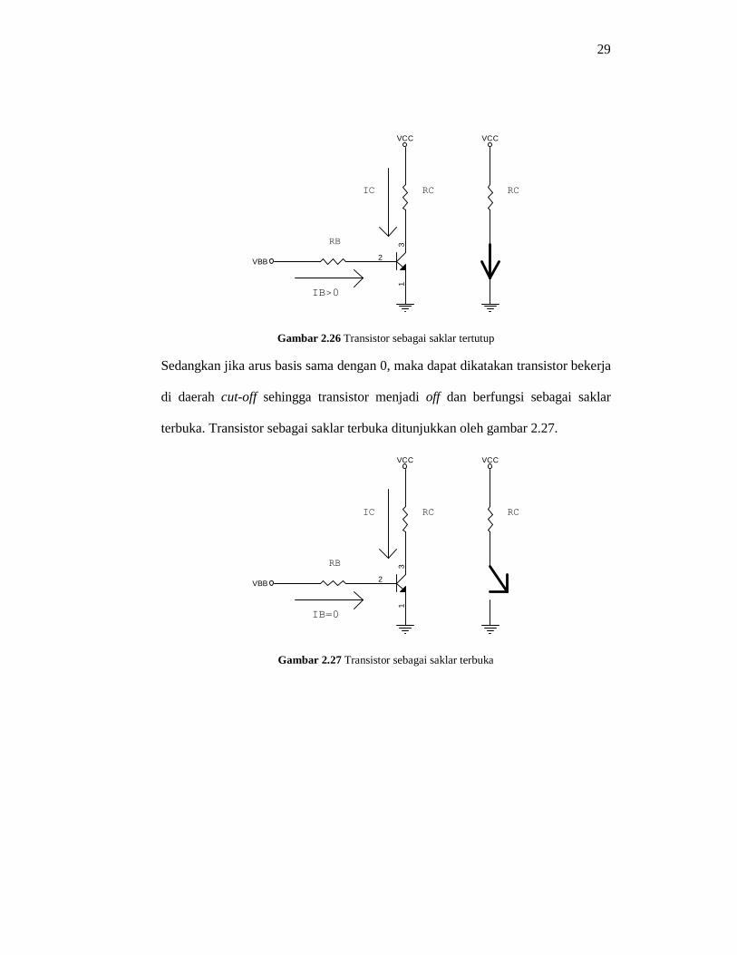
29
VCC VCC
RC
RB
VBB
3
2
1
IC
IB>0
RC
Gambar 2.26 Transistor sebagai saklar tertutup
Sedangkan jika arus basis sama dengan 0, maka dapat dikatakan transistor bekerja
di daerah cut-off sehingga transistor menjadi off dan berfungsi sebagai saklar
terbuka. Transistor sebagai saklar terbuka ditunjukkan oleh gambar 2.27.
3
2
1
RC
VCC
VBB
VCC
IB=0
RB
IC RC
Gambar 2.27 Transistor sebagai saklar terbuka
30
BAB III
RANCANGAN PENELITIAN
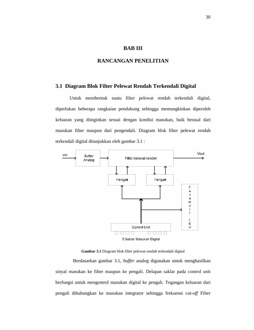
3.1 Diagram Blok Filter Pelewat Rendah Terkendali Digital
Untuk membentuk suatu filter pelewat rendah terkendali digital,
diperlukan beberapa rangkaian pendukung sehingga memungkinkan diperoleh
keluaran yang diinginkan sesuai dengan kondisi masukan, baik berasal dari
masukan filter maupun dari pengendali. Diagram blok filter pelewat rendah
terkendali digital ditunjukkan oleh gambar 3.1 :
Gambar 3.1 Diagram blok filter pelewat rendah terkendali digital
Berdasarkan gambar 3.1, buffer analog digunakan untuk menghasilkan
sinyal masukan ke filter maupun ke pengali. Delapan saklar pada control unit
berfungsi untuk mengontrol masukan digital ke pengali. Tegangan keluaran dari
pengali dihubungkan ke masukan integrator sehingga frekuensi cut-off Filter
31
Pelewat Rendah dapat diubah-ubah. Pengali berfungsi untuk menghasilkan
tegangan keluaran sebagai fungsi perkalian antara suatu konstanta dengan
tegangan masukan.
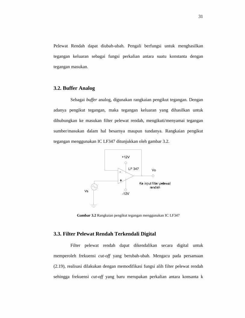
3.2. Buffer Analog
Sebagai buffer analog, digunakan rangkaian pengikut tegangan. Dengan
adanya pengikut tegangan, maka tegangan keluaran yang dihasilkan untuk
dihubungkan ke masukan filter pelewat rendah, mengikuti/menyamai tegangan
sumber/masukan dalam hal besarnya maupun tundanya. Rangkaian pengikut
tegangan menggunakan IC LF347 ditunjukkan oleh gambar 3.2.
Gambar 3.2 Rangkaian pengikut tegangan menggunakan IC LF347
3.3. Filter Pelewat Rendah Terkendali Digital
Filter pelewat rendah dapat dikendalikan secara digital untuk
memperoleh frekuensi cut-off yang berubah-ubah. Mengacu pada persamaan
(2.19), realisasi dilakukan dengan memodifikasi fungsi alih filter pelewat rendah
sehingga frekuensi cut-off yang baru merupakan perkalian antara konsanta k

32
dengan frekuensi cut-off semula (ωo). Pernyataan ini ditunjukkan oleh persamaan
(3.6) :
( )2
002
200 )(
ωωω
ksQ
ks
kA
V
V
i
lp
++= (3.6)
Diagram blok untuk mengimplementasikan persamaan diatas adalah :
soω
−s
oω−
Q
1
ΣΣoA
Gambar 3.3 Diagram blok yang mempresentasikan persamaan (3.6)
Berdasarkan gambar 3.3, untuk memperoleh perubahan frekuensi cut-off,
rangkaian pengali dihubungkan sebelum integrator pada rangkaian filter. Karena
dikendalikan secara digital, maka pada pengali ditambahkan komponen yang
dapat mengubah sinyal digital menjadi sinyal analog, yaitu Digital to Analog
Converter (DAC). Frekuensi cut-off filter pelewat rendah dapat ditala secara
digital tergantung pada besar nilai konstanta k yang merupakan kode kendali
digital, dengan nilai k tergantung dari bit-bit masukan. Modul integrator
mempunyai karakteristik transfer sebesar –k ωo/s. Frekuensi cut-off yang baru
adalah sebesar ωo’= k. ωo. Semakin besar nilai bit yang dimasukkan ke pengali,
maka frekuensi cut-off juga semakin meningkat, begitu pula sebaliknya.
33
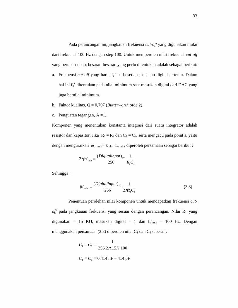
Pada perancangan ini, jangkauan frekuensi cut-off yang digunakan mulai
dari frekuensi 100 Hz dengan step 100. Untuk memperoleh nilai frekuensi cut-off
yang berubah-ubah, besaran-besaran yang perlu ditentukan adalah sebagai berikut:
a. Frekuensi cut-off yang baru, fo’ pada setiap masukan digital tertentu. Dalam
hal ini fo’ ditentukan pada nilai minimum saat masukan digital dari DAC yang
juga bernilai minimum.
b. Faktor kualitas, Q = 0,707 (Butterworth orde 2).
c. Penguatan tegangan, A =1.
Komponen yang menentukan konstanta integrasi dari suatu integrator adalah
resistor dan kapasitor. Jika R1 = R2 dan C1 = C2, serta mengacu pada point a, yaitu
dengan menguraikan ωo’ min= kmin. ωo min, diperoleh persamaan sebagai berikut :
11
10min
1
256
)('2
CR
utDigitalinpfo =π
Sehingga :
11
10min 2
1
256
)('
CR
utDigitalinpfo
π= (3.8)
Penentuan perolehan nilai komponen untuk mendapatkan frekuensi cut-
off pada jangkauan frekuensi yang sesuai dengan perancangan. Nilai R1 yang
digunakan = 15 KΩ, masukan digital = 1 dan fo’min = 100 Hz. Dengan
menggunakan persamaan (3.8) diperoleh nilai C1 dan C2 sebesar :
100.15.2.256
121 K
CCπ
==
== 21 CC 0.414 nF = 414 pF
34
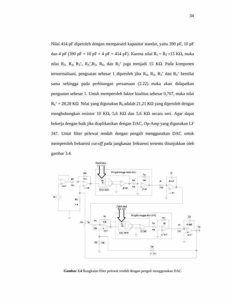
Nilai 414 pF diperoleh dengan mempararel kapasitor standar, yaitu 390 pF, 10 pF
dan 4 pF (390 pF + 10 pF + 4 pF = 414 pF). Karena nilai R1 = R2 =15 KΩ, maka
nilai R3, R4, R3’, R4’,R5, R6, dan R5’ juga menjadi 15 KΩ. Pada komponen
ternormalisasi, penguatan sebesar 1 diperoleh jika R4, R3, R3’ dan R4’ bernilai
sama sehingga pada perhitungan persamaan (2.22) maka akan didapatkan
penguatan sebesar 1. Untuk memperoleh faktor kualitas sebesar 0,707, maka nilai
R6’ = 28,28 KΩ Nilai yang digunakan R6 adalah 21,21 KΩ yang diperoleh dengan
menghubungkan resistor 10 KΩ, 5,6 KΩ dan 5,6 KΩ secara seri. Agar dapat
bekerja dengan baik jika diaplikasikan dengan DAC, Op-Amp yang digunakan LF
347. Untai filter pelewat rendah dengan pengali menggunakan DAC untuk
memperoleh frekuensi cut-off pada jangkauan frekuensi tertentu ditunjukkan oleh
gambar 3.4.
Gambar 3.4 Rangkaian filter pelewat rendah dengan pengali menggunakan DAC

35
3.4. Penampil LED
Rangkaian penampil sangat penting untuk memvisualisasikan dan untuk
mengetahui data-data yang dimasukan ke rangkaian DAC. Agar dapat diketahui
masukan digital ke DAC, sebagai penampil digunakan rangkaian penampil LED.
LED akan menyala cukup terang bila dialiri arus sebesar 10 mA sampai
20 mA. Bila dialiri arus yang lebih besar lagi, maka LED akan menyala lebih
terang. Arus maksimal yang diperbolehkan adalah antara 25 mA sampai 100 mA,
yang tergantung dari tipe dan warna LED. Untuk dapat mengetahui kondisi LED,
digunakan saklar transistor. Kondisi transistor (aktif atau tidak aktif) sangat
dipengaruhi oleh arus IB dan besarnya arus IB tergantung dari Vcc yang
dihubungkan dari saklar. Gambar 3.5 menunjukkan rangkaian saklar transistor
untuk menyalakan LED.
LED
VCC
VCC DARI SAKLAR
RB
Q
3
2
1
RC
Gambar 3.5 Rangkaian saklar transistor untuk menyalakan LED
VCC dari saklar adalah sebesar 5 V dan VCC adalah sebesar 5 V. Sedangkan
transistor yang digunakan mempunyai penguatan arus (β) yang besar, yaitu
transistor BC109. Agar LED dapat menyala cukup terang dan transistor dalam

36
keadaan jenuh/saturasi maka berdasarkan data sheet, dipilih nilai IC sebesar 20
mA. Nilai Rc diperoleh berdasarkan persamaan :
( ) )(satceddcccc VVRRIV +++=
dC
satcedccc R
I
VVVR −
−−= )(
Vd adalah tegangan potong (cut-in voltage) LED yang mempunyai nilai sekitar 2
V, sedangkan Rd adalah hambatan ekuivalen dc. Karena nilai Rd dan VCE(sat)
sangat kecil, sehingga dapat diabaikan, maka diperoleh :
C
dccc I
VVR
−=
mA
VV
20
25 −=
Ω= 150cR
Nilai Rc standar yang dipilih juga bernilai 150 Ω.
Transistor yang digunakan berfungsi sebagai saklar tertutup saat
masukan digital saklar ON dan saklar terbuka saat masukan digital saklar OFF.
Saat masukan digital saklar ON (logika tinggi), maka kolektor terhubung ke
emitter sehingga arus akan mengalir dari Vcc ke ground dan LED menjadi
menyala. Sedangkan saat masukan digital saklar OFF (logika rendah), maka
kolektor menjadi terbuka terhadap emitter sehingga arus dari Vcc tidak dapat
mengalir ke ground dan LED menjadi padam.
Transistor yang digunakan berfungsi sebagai saklar tertutup saat VOH
dan saklar terbuka saat VOL. Saat VOH (logika tinggi), maka kolektor terhubung ke
emitter sehingga arus akan mengalir dari Vcc ke ground dan LED menjadi

37
menyala. Sedangkan saat VOL (logika rendah), maka kolektor menjadi terbuka
terhadap emitter sehingga arus dari Vcc tidak dapat mengalir ke ground dan LED
menjadi padam. Berdasarkan data sheet, β yang dipilih adalah sebesar 350. β
dapat digunakan untuk mendapatkan nilai IB0, yaitu berdasarkan persamaan :
β
)(0
satCB
II =
Sehingga :
AmA
I B µ14,57350
200 ==
IB0 merupakan besaran arus yang menyebabkan transistor menjadi saturasi. Besar
IB yang digunakan untuk mengaktifkan transistor dipilih sebesar 10.IB0, yaitu
0,5714 mA. Agar diperoleh nilai IB yang diinginkan, maka diperlukan hambatan
Rb, yang didapat dari persamaan :
B
beOHb I
VVR
−=
VOH ditentukan sebesar 4,3 V dan Vbe transistor jenis silikon adalah sebesar 0,7
V, sehingga :
Ω=−= KmA
VVRb 08,7
5714,0
7,075,4
Nilai Rb standar yang dipilih adalah 6,8 KΩ.
Gambar rangkaian penampil LED ditunjukkan pada gambar 3.6

38
Masukan digital dari saklar kendali
Gambar 3.6 Gambar rangkaian penampil LED
3.5. Saklar Sebagai Kendali Masukan Digital
Sebagai masukan digital berupa binary code 8 bit digunakan delapan
saklar yang dihubungkan dengan Vcc 5 Volt. Saklar yang digunakan adalah switch
SPDT.
Gambar 3.7 Rangkaian saklar masukan digital
39
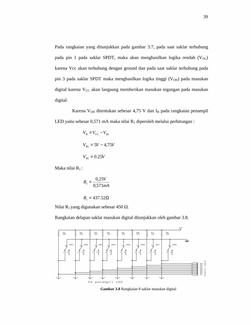
Pada rangkaian yang ditunjukkan pada gambar 3.7, pada saat saklar terhubung
pada pin 1 pada saklar SPDT, maka akan menghasilkan logika rendah (VOL)
karena Vcc akan terhubung dengan ground dan pada saat saklar terhubung pada
pin 3 pada saklar SPDT maka menghasilkan logika tinggi (VOH) pada masukan
digital karena VCC akan langsung memberikan masukan tegangan pada masukan
digital.
Karena VOH ditentukan sebesar 4,75 V dan IB pada rangkaian penampil
LED yaitu sebesar 0,571 mA maka nilai R1 diperoleh melalui perhitungan :
1RCCB VVV −=
VVVR 75,451 −=
VVR 25.01 =
Maka nilai R1 :
mA
VR
571,0
25,01 =
Ω= 52.4371R
Nilai R1 yang digunakan sebesar 450 Ω.
Rangkaian delapan saklar masukan digital ditunjukkan oleh gambar 3.8.
SW12
1 3
R4450
D6
D1
D7
SW52
1 3
R1450
D0
D3
SW42
1 3
SW82
1 3
5 V
R6450
R8450
digital input
SW22
1 3
R5450
D2
SW72
1 3
D4
ke penampil LED
R7450
R3450
SW32
1 3
SW62
1 3
R2450
D5
Gambar 3.8 Rangkaian 8 saklar masukan digital
40
BAB IV
HASIL PENGAMATAN DAN PEMBAHASAN
Pada bab ini akan ditunjukkan hasil pengamatan dan pembahasan dari
Filter Pelewat Rendah Terkendali Digital. Pengujian dilakukan dengan cara
memberikan masukan frekuensi pada masukan blok filter yang berupa gelombang
sinus dari AFG (Audio Function Generator) serta masukan pengendali frekuensi
berupa bit digital yang berasal dari saklar. Jumlah saklar untuk kendali masukan
digital ada 8 saklar, yaitu saklar1 (LSB), saklar2, saklar3, saklar4, saklar5, saklar6,
saklar7 dan saklar8 (MSB). Untuk penampil nilai bit masukan digital, digunakan
LED yang jumlahnya ada 8 LED. Pada saat saklarn tidak terhubung ke ground ,
maka nilai bit masukan digital akan ditampilkan dengan LED ke n yang menyala
sebagai bit 1 dan saat saklarn terhubung ke ground, maka nilai bit masukan digital
akan ditampilkan dengan LED ke n yang tidak menyala sebagai bit 0. Tegangan
dan frekuensi yang dihasilkan pada keluaran filter digunakan sebagai acuan dalam
membuat grafik tanggapan magnitude.
4.1. Tanggapan Magnitude Sebagai Fungsi Frekuensi
Sub bab ini bertujuan untuk menunjukkan tanggapan magnitude dari
keluaran filter pelewat rendah. Jumlah masukan digital ada 255 masukan digital,
sehingga jumlah filter pelewat rendah ada 255 dimana frekuensi cut-off nya
terkendali oleh masukan digital. Berdasarkan jumlah filter pelewat rendah, maka
tanggapan magnitude pada filter pelewat rendah juga ada 255 dimana frekuensi

41
cut-off nya urut berdasarkan masukan digital dari nilai yang terkecil (urutan ke 1
(fc=100 Hz)) sampai masukan digital yang terbesar (urutan ke 255 (fc 25,5 KHz)).
Untuk pengamatan diambil beberapa percobaan, yaitu percobaan pada urutan
rendah (urutan ke 1 (fc = 100Hz), urutan ke 2 (fc = 200Hz) dan urutan ke 3 (fc =
300 Hz)), urutan sedang (urutan ke 100 (fc = 10 KHz), urutan ke 101 (fc = 10,1
KHz) dan urutan ke 102 (fc = 10,2 KHz)) dan urutan tinggi (urutan ke 253 (fc =
25,3 KHz), urutan ke 254 (fc = 25,4 KHz) dan urutan ke 255 (fc = 25,5 KHz))
sesuai dengan nilai masukan digital yang dimasukkan ke rangkaian pengali.
Pengaturan saklar untuk masukan digital pada percobaan dapat ditunjukkan oleh
tabel 4.1.
Tabel 4.1 Konfigurasi saklar masukan digital saat pengamatan tanggapan magnitude
Masukan Digital
(MSB) (LSB) Urutan
S8 S7 S6 S5 S4 S3 S2 S1
ke 1 0 0 0 0 0 0 0 1
ke 2 0 0 0 0 0 0 1 0 Urutan
Rendah
ke 3 0 0 0 0 0 0 1 1
ke 100 0 1 1 0 0 1 0 0
ke 101 0 1 1 0 0 1 0 1 Urutan
Sedang
ke 102 0 1 1 0 0 1 1 0
ke 253 1 1 1 1 1 1 0 1
ke 254 1 1 1 1 1 1 1 0 Urutan
Tinggi
ke 255 1 1 1 1 1 1 1 1

42
Untuk memperoleh grafik tanggapan magnitude, penguatan amplitudo
hasil pengamatan dihitung dengan menggunakan persamaan (4.1) :
I
OdB V
VM 10log20)( =ω (4.1)
Sedangkan secara teoritis, penguatan amplitudo dihitung berdasarkan persamaan
(2.13). Dari tanggapan magnitude tersebut, dapat ditunjukkan frekuensi cut-off
yang berubah dari nilai masukan digital yang rendah ke nilai masukan digital yang
lebih tinggi. Jika hasil pengamatan tegangan (Vpp) keluaran dan tegangan
masukan (Vpp) untuk frekuensi tertentu pada percobaan pada urutan rendah
(urutan ke 1 (fc = 100Hz), urutan ke 2 (fc = 200Hz) dan urutan ke 3 (fc = 300
Hz)), urutan sedang (urutan ke 100 (fc = 10 KHz), urutan ke 101 (fc = 10,1 KHz)
dan urutan ke 102 (fc = 10,2 KHz)) dan urutan tinggi (urutan ke 253 (fc = 25,3
KHz), urutan ke 254 (fc = 25,4 KHz) dan urutan ke 255 (fc = 25,5 KHz))
dimasukkan ke persamaan (4.1) maka diperoleh tanggapan amplitudo relatif MdB
(ω) yang terdapat pada tabel 4.2, 4.3, 4.4, dan untuk tanggapan amplitudo relatif
MdB (ω) secara teoritis nilai frekuensi hasil pengamatan dan nilai frekuensi cut-off
dimasukkan ke persamaan (2.13).
Tanggapan amplitudo relatif MdB (ω) hasil pengamatan untuk urutan
rendah dapat ditunjukkan oleh tabel 4.2.
Tabel 4.2 Tanggapan amplitudo relatif MdB (ω) pengamatan untuk urutan rendah
Tanggapan Amplitudo (dB) Frekuensi
(Hz) urutan ke 1 (fc =100 Hz)
urutan ke 2 (fc =200 Hz)
urutan ke 3 (fc =300 Hz)
10 -0,211 -0,211 -0,211 40 -0,069 0 0
60,2 -0,5 0 0
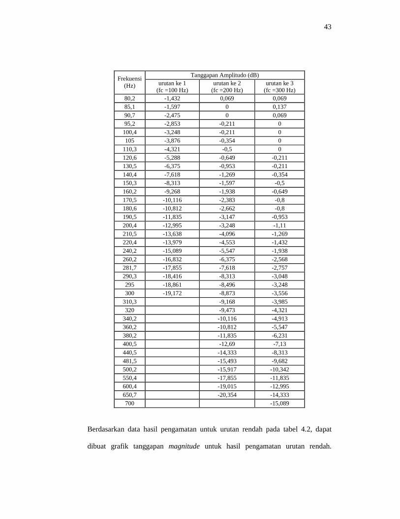
43
Tanggapan Amplitudo (dB) Frekuensi
(Hz) urutan ke 1 (fc =100 Hz)
urutan ke 2 (fc =200 Hz)
urutan ke 3 (fc =300 Hz)
80,2 -1,432 0,069 0,069 85,1 -1,597 0 0,137 90,7 -2,475 0 0,069 95,2 -2,853 -0,211 0
100,4 -3,248 -0,211 0 105 -3,876 -0,354 0
110,3 -4,321 -0,5 0 120,6 -5,288 -0,649 -0,211 130,5 -6,375 -0,953 -0,211 140,4 -7,618 -1,269 -0,354 150,3 -8,313 -1,597 -0,5 160,2 -9,268 -1,938 -0,649 170,5 -10,116 -2,383 -0,8 180,6 -10,812 -2,662 -0,8 190,5 -11,835 -3,147 -0,953 200,4 -12,995 -3,248 -1,11 210,5 -13,638 -4,096 -1,269 220,4 -13,979 -4,553 -1,432 240,2 -15,089 -5,547 -1,938 260,2 -16,832 -6,375 -2,568 281,7 -17,855 -7,618 -2,757 290,3 -18,416 -8,313 -3,048 295 -18,861 -8,496 -3,248 300 -19,172 -8,873 -3,556
310,3 -9,168 -3,985 320 -9,473 -4,321
340,2 -10,116 -4,913 360,2 -10,812 -5,547 380,2 -11,835 -6,231 400,5 -12,69 -7,13
440,5 -14,333 -8,313 481,5 -15,493 -9,682 500,2 -15,917 -10,342 550,4 -17,855 -11,835 600,4 -19,015 -12,995 650,7 -20,354 -14,333 700 -15,089
Berdasarkan data hasil pengamatan untuk urutan rendah pada tabel 4.2, dapat
dibuat grafik tanggapan magnitude untuk hasil pengamatan urutan rendah.

44
Gambar 4.1 menunjukkan tanggapan magnitude hasil pengamatan urutan rendah
(dari urutan 1 sampai urutan 3).
-21
-18
-15
-12
-9
-6
-3
0
3
10 100 1000
Frekuensi (Hz)
Peng
uata
n A
mpl
itud
o (d
B)
fc = 100 Hz fc = 200 Hz fc = 300 Hz
Gambar 4.1. Tanggapan magnitude hasil pengamatan dari urutan 1 sampai urutan 3
Berdasarkan tanggapan magnitude hasil pengamatan pada gambar 4.1 terlihat
bahwa frekuensi cut-off adalah sebesar 95 Hz saat urutan ke 1, sebesar 187,5 Hz
saat urutan ke 2 dan 280,4 Hz saat urutan ke 3.
Tanggapan amplitudo relatif MdB (ω) secara teoritis untuk urutan rendah dapat
ditunjukkan oleh tabel 4.3.
Tabel 4.3 Tanggapan amplitudo relatif MdB (ω) teoritis untuk urutan rendah
Tanggapan Amplitudo (dB) Frekuensi
(Hz) urutan ke 1 (fc =100 Hz)
urutan ke 2 (fc =200 Hz)
urutan ke 3 (fc =300 Hz)
10 0 0 0 40 -0,109 -0,006 -0,001
60,2 -0,535 -0,035 -0,007 80,2 -1,503 -0,11 -0,022
85,1 -1,831 -0,14 -0,028

45
Tanggapan Amplitudo (dB) Frekuensi
(Hz) urutan ke 1 (fc =100 Hz)
urutan ke 2 (fc =200 Hz)
urutan ke 3 (fc =300 Hz)
90,7 -2,244 -0,179 -0,036 95,2 -2,604 -0,217 -0,043
100,4 -3,045 -0,267 -0,054 105 -3,454 -0,317 -0,064
110,3 -3,944 -0,384 -0,078 120,6 -4,935 -0,539 -0,111
130,5 -5,91 -0,723 -0,152 140,4 -6,889 -0,944 -0,203 150,3 -7,855 -1,202 -0,265 160,2 -8,8 -1,497 -0,339 170,5 -9,754 -1,841 -0,43 180,6 -10,658 -2,213 -0,535 190,5 -11,513 -2,608 -0,654 200,4 -12,337 -3,027 -0,788 210,5 -13,145 -3,477 -0,942 220,4 -13,908 -3,935 -1,11 240,2 -15,351 -4,886 -1,495 260,2 -16,706 -5,871 -1,947 281,7 -18,059 -6,933 -2,497 290,3 -18,574 -7,355 -2,734 295 -18,849 -7,584 -2,866 300 -19,138 -7,826 -3,01
310,3 -8,321 -3,313 320 -8,781 -3,606
340,2 -9,718 -4,238 360,2 -10,614 -4,882 380,2 -11,479 -5,538 400,5 -12,324 -6,207 440,5 -13,897 -7,519 481,5 -15,39 -8,828
500,2 -16,034 -9,409 550,4 -17,654 -10,909 600,4 -19,149 -12,315 650,7 -20,532 -13,642 700 -14,863
Berdasarkan tabel 4.3, dapat dibuat grafik tanggapan magnitude untuk urutan
rendah untuk hasil secara teoritis. Gambar 4.2 menunjukkan tanggapan magnitude
secara teoritis dari urutan ke 1 sampai urutan ke 3.
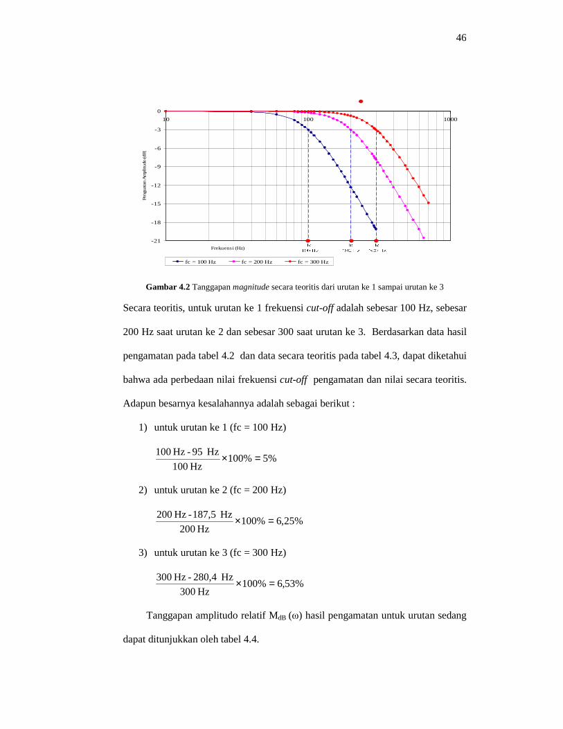
46
-21
-18
-15
-12
-9
-6
-3
0
10 100 1000
Frekuensi (Hz)
Peng
uata
n A
mpl
itud
o (d
B)
fc = 100 Hz fc = 200 Hz fc = 300 Hz
Gambar 4.2 Tanggapan magnitude secara teoritis dari urutan ke 1 sampai urutan ke 3
Secara teoritis, untuk urutan ke 1 frekuensi cut-off adalah sebesar 100 Hz, sebesar
200 Hz saat urutan ke 2 dan sebesar 300 saat urutan ke 3. Berdasarkan data hasil
pengamatan pada tabel 4.2 dan data secara teoritis pada tabel 4.3, dapat diketahui
bahwa ada perbedaan nilai frekuensi cut-off pengamatan dan nilai secara teoritis.
Adapun besarnya kesalahannya adalah sebagai berikut :
1) untuk urutan ke 1 (fc = 100 Hz)
%5%100Hz 100
Hz 95 -Hz 100 =×
2) untuk urutan ke 2 (fc = 200 Hz)
%25,6%100Hz 200
Hz 187,5 -Hz 200 =×
3) untuk urutan ke 3 (fc = 300 Hz)
%53,6%100Hz 300
Hz 280,4 -Hz 300 =×
Tanggapan amplitudo relatif MdB (ω) hasil pengamatan untuk urutan sedang
dapat ditunjukkan oleh tabel 4.4.

47
Tabel 4.4 Tanggapan amplitudo relatif MdB (ω) pengamatan untuk urutan sedang
Tanggapan Amplitudo (dB) Frekuensi
(Hz) urutan ke 100 (fc = 10 KHz)
urutan ke 101 (fc = 10,1 KHz)
urutan ke 102 (fc = 10,2 KHz)
50,4 0,137 0 0,137 100,3 0,34 0,34 0,34 200,7 0,205 0 0,205 400,2 0 0 0,137 600,6 0 0 0 800,9 0 0 0 1003 0 0 0 1506 0 0 0 1826 0 0 0 2052 0 0 0
3028 0 0 0 3534 0 0 0 4026 0 0 0 4512 -0,069 -0,069 0 5015 -0,354 -0,354 -0,211 5508 -0,5 -0,5 -0,354 6054 -0,649 -0,649 -0,5 6551 -0,915 -0,915 -0,8 7030 -1,26 -1,26 -1,11 7504 -1,43 -1,43 -1,26 8016 -1,93 -1,93 -1,76 8504 -2,29 -2,113 -2,113 9060 -2,66 -2,568 -2,47 9513 -2,95 -3,14 -2,8 10032 -3,248 -3,248 -2,95 10088 -3,34 -3,298 -3,248 10100 -3,452 -3,248 -3,452 10210 -3,715 -3,248 -3,452 10508 -4,32 -4,09 -3,66 11007 -4,43 -4,32 -4,09 11530 -5,03 -4,79 -4,67 12090 -5,67 -5,41 -5,28 13520 -7,13 -6,82 -6,82 14032 -7,61 -7,29 -7,29
15070 -8,49 -8,31 -8,13 15504 -8,87 -8,49 -8,49 16118 -9,26 -9,06 -9,06 17070 -10,22 -9,89 -9,68 18050 -11,05 -10,57 -10,34 19040 -11,56 -11,56 -11,3 20064 -12,69 -12,395 -12,11 20210 -12,841 -12,841 -12,541

48
Tanggapan Amplitudo (dB) Frekuensi
(Hz) urutan ke 100 (fc = 10 KHz)
urutan ke 101 (fc = 10,1 KHz)
urutan ke 102 (fc = 10,2 KHz)
20410 -12,995 -12,995 -12,841 21030 -13,473 -13,31 -12,995 23075 -14,703 -14,516 -13,979 24020 -15,08 -14,89 -14,7 26040 -16,59 -16,13 -16,13 28060 -17,58 -17,32 -17,07
30111 -18,13 -18,13 -17,85 28060 -17,58 -17,32 -17,07 30111 -18,13 -18,13 -17,85
Berdasarkan data hasil pengamatan untuk urutan rendah pada tabel 4.4, dapat
dibuat grafik tanggapan magnitude untuk hasil pengamatan urutan sedang.
Gambar 4.3 menunjukkan tanggapan magnitude hasil pengamatan urutan sedang
(dari urutan 100 sampai urutan 102).
-21
-18
-15
-12
-9
-6
-3
0
3
100 1000 10000 100000
Frekuensi (Hz)
Peng
uata
n A
mpl
itud
o (d
B)
fc = 10000 Hz fc = 10100 Hz fc = 10200 Hz
Gambar 4.3 Tanggapan magnitude hasil pengamatan untuk dari urutan ke 100 sampai urutan ke 102
Berdasarkan tanggapan magnitude hasil pengamatan pada gambar 4.3 terlihat
bahwa frekuensi cut-off adalah sebesar 9800 Hz saat urutan ke 100, sebesar 9950
Hz saat urutan ke 101 dan 10060 Hz saat urutan ke 102.
49
Tanggapan amplitudo relatif MdB (ω) secara teoritis untuk urutan sedang
dapat ditunjukkan oleh tabel 4.5.
Tabel 4.5 Tanggapan amplitudo relatif MdB (ω) teoritis untuk urutan sedang
Tanggapan Amplitudo (dB) Frekuensi
(Hz) urutan ke 100 (fc = 10 KHz)
urutan ke 101 (fc = 10,1 KHz)
urutan ke 102 (fc = 10,2 KHz)
50,4 0 0 0 100,3 0 0 0 200,7 0 0 0 400,2 0 0 0 600,6 -0,00005 -0,00005 -0,00005 800,9 -0,00017 -0,00017 -0,00016 1003 -0,0004 -0,00042 -0,0004 1506 -0,0022 -0,0021 -0,002 1826 -0,0048 -0,0046 -0,0044 2052 -0,0076 -0,0073 -0,0071 3028 -0,036 -0,034 -0,033 3534 -0,067 -0,064 -0,062 4026 -0,112 -0,108 -0,104 4512 -0,176 -0,169 -0,163 5015 -0,266 -0,256 -0,246 5508 -0,382 -0,368 -0,354
6054 -0,714 -0,527 -0,508 6551 -0,734 -0,707 -0,682 7030 -0,949 -0,915 -0,883 7504 -1,196 -1,155 -1,115 8016 -1,501 -1,451 -1,4033 8504 -1,826 -1,768 -1,711 9060 -2,236 -2,168 -2,101 9513 -2,598 -2,521 -2,446
10032 -3,038 -2,952 -2,868 10088 -3,087 -2,999 -2,915 10100 -3,097 -3,01 -2,925 10210 -3,194 -3,105 -3,276 10508 -3,461 -3,367 -3,276 11007 -3,923 -3,821 -3,721 11530 -4,42 -4,311 -4,204 12090 -4,964 -4,847 -4,733 13520 -6,376 -6,243 -6,113 14032 -6,881 -6,744 -6,61 15070 -7,894 -7,749 -7,607 15504 -8,31 -8,164 -8,019 16118 -8,892 -8,742 -8,594
50
Tanggapan Amplitudo (dB) Frekuensi
(Hz urutan ke 100 (fc = 10 KHz)
urutan ke 101 (fc = 10,1 KHz)
urutan ke 102 (fc = 10,2 KHz)
17070 -9,772 -9,618 -9,466 18050 -10,65 -10,492 -10,336 19040 -11,505 -11,344 -11,186 20064 -12,356 -12,194 -12,033 20210 -12,475 -12,312 -12,151 20410 -12,637 -12,473 -12,312
21030 -13,13 -12,965 -12,803 23075 -14,676 -14,509 -14,344 24020 -15,351 -15,183 -15,017 26040 -16,719 -16,549 -16,382 28060 -17,993 -17,822 -17,654 30111 -19,201 -19,03 -18,861
Berdasarkan tabel 4.5, dapat dibuat grafik tanggapan magnitude untuk urutan
sedang untuk hasil secara teoritis. Gambar 4.4 menunjukkan tanggapan magnitude
secara teoritis dari urutan ke 100 sampai urutan ke 102.
-21
-18
-15
-12
-9
-6
-3
0
3
100 1000 10000 100000
Frekuensi (Hz)
Peng
uata
n A
mpl
itud
o (d
B)
fc = 10000 Hz fc = 10100 Hz fc = 10200 Hz
Gambar 4.4 Tanggapan magnitude secara teoritis dari urutan ke 101 sampai urutan ke 102
Secara teoritis untuk urutan ke 100 frekuensi cut-off adalah sebesar 1000 Hz,
sebesar 10100 Hz saat urutan ke 101 dan sebesar 10200 saat urutan ke 102.
Berdasarkan data hasil pengamatan pada tabel 4.4 dan data secara teoritis pada
51
tabel 4.5, dapat diketahui bahwa ada perbedaan nilai frekuensi cut-off
pengamatan dan nilai secara teoritis. Adapun besarnya kesalahannya adalah
sebagai berikut :
1) untuk urutan ke 100 (fc = 10 KHz)
%5%100Hz 10000
Hz 9800 -Hz 10000 =×
2) untuk urutan ke 101 (fc = 10,1 KHz)
%48,1%100Hz 10100
Hz 9950 -Hz 10100 =×
3) untuk urutan ke 102 (fc = 10,2 KHz)
%37,1%100Hz 10200
Hz 10060 -Hz 10200 =×
Tanggapan amplitudo relatif MdB (ω) hasil pengamatan untuk urutan
tinggi dapat ditunjukkan oleh tabel 4.6.
Tabel 4.6 Tanggapan amplitudo relatif MdB (ω) pengamatan untuk urutan tinggi
Tanggapan Amplitudo (dB) Frekuensi
(Hz) urutan ke 255 (fc = 25,5 KHz)
urutan ke 254 (fc = 25,4 KHz)
urutan ke 253 (fc = 25,3 KHz)
141,6 0 0 0 200,7 0 0 0 300,6 0 0 0 400,6 0 0 0 501,7 0 0 0 600,6 0 0 0 700,2 0 0 0 803,2 0 -0,034 -0,034 904,7 -0,034 -0,069 -0,069 1006 -0,034 -0,069 -0,069 1509 -0,034 -0,069 -0,069 2010 -0,069 -0,069 -0,069 2535 -0,069 -0,104 -0,104 3009 -0,069 -0,104 -0,14 3512 -0,069 -0,104 -0,14
4042 -0,069 -0,104 -0,14

52
Tanggapan Amplitudo (dB) Frekuensi
(Hz) urutan ke 255 (fc = 25,5 KHz)
urutan ke 254 (fc = 25,4 KHz)
urutan ke 253 (fc = 25,3 KHz)
4507 -0,069 -0,14 -0,14 5022 -0,104 -0,14 -0,14 6030 -0,104 -0,14 -0,175 7009 -0,104 -0,14 -0,175 8064 -0,14 -0,175 -0,211 9015 -0,14 -0,175 -0,211
10075 -0,211 -0,246 -0,318 12021 -0,211 -0,246 -0,318 15088 -0,427 -0,5 -0,574 17046 -0,8 -0,876 -0,953 20100 -1,432 -1,514 -1,597 22060 -1,938 -2,025 -2,113 23500 -2,383 -2,475 -2,475 24004 -2,475 -2,521 -2,568 24834 -2,757 -2,853 -2,853 25040 -2,853 -2,853 -2,95 25305 -2,853 -2,95 -2,999 25420 -2,853 -3,048 -3,048 25510 -2,95 -3,048 -3,048 25762 -3,048 -3,147 -3,248 26084 -3,048 -3,147 -3,349 26513 -3,349 -3,452 -3,556 27092 -3,609 -3,661 -3,661 28030 -3,876 -3,985 -4,096 30064 -4,553 -4,671 -4,791 33064 -5,679 -5,814 -5,882 35096 -6,521 -6,595 -6,669 40134 -8,313 -8,404 -8,496 43060 -9,37 -9,473 -9,577 45020 -10,006 -10,116 -10,399
50030 -11,308 -11,308 -11,835 50620 -11,437 -11,567 -11,835 50807 -11,567 -11,835 -12,11 51040 -11,835 -12,11 -12,11 52020 -12,11 -12,11 -12,395
Berdasarkan data hasil pengamatan untuk urutan tinggi pada tabel 4.6, dapat
dibuat grafik tanggapan magnitude untuk hasil pengamatan urutan tinggi. Gambar

53
4.5 menunjukkan tanggapan magnitude hasil pengamatan untuk urutan tinggi (dari
urutan 253 sampai urutan 255).
-14
-12
-10
-8
-6
-4
-2
0
2
100 1000 10000 100000
Frekuensi (Hz)
Peng
uata
n A
mpl
itudo
(dB
)
fc = 25500 Hz fc = 25400 Hz fc = 25300 Hz
Gambar 4.5 Tanggapan magnitude hasil pengamatan untuk dari urutan ke 253 sampai urutan ke 255
Berdasarkan tanggapan magnitude hasil pengamatan pada gambar 4.5 terlihat
bahwa frekuensi cut-off adalah sebesar 25305 Hz saat urutan ke 253, sebesar
25420 Hz saat urutan ke 254 dan 25510 Hz saat urutan ke 255.
Tanggapan amplitudo relatif MdB (ω) secara teoritis untuk urutan tinggi
dapat ditunjukkan oleh tabel 4.7.
Tabel 4.7 Tanggapan amplitudo relatif MdB (ω) teoritis untuk urutan tinggi
Tanggapan Amplitudo (dB) Frekuensi
(Hz) urutan ke 255 (fc = 25,5 KHz)
urutan ke 254 (fc = 25,4 KHz)
urutan ke 253 (fc = 25,3 KHz)
141,6 0 0 0 200,7 0 0 0 300,6 0 0 0
54
Tanggapan Amplitudo (dB) Frekuensi
(Hz) urutan ke 255 (fc = 25,5 KHz)
urutan ke 254 (fc = 25,4 KHz)
urutan ke 253 (fc = 25,3 KHz)
400,6 0 0 0 501,7 0 0 0 600,6 0 0 0 700,2 0 0 0 803,2 0 0 0 904,7 0 0 0
1006 -0,00001 -0,00001 -0,00001 1509 -0,00005 -0,00005 -0,00005 2010 -0,00016 -0,00017 -0,00017 2535 -0,00042 -0,00043 -0,00043 3009 -0,00084 -0,00085 -0,00086 3512 -0,00156 -0,00158 -0,00161 4042 -0,002 -0,002 -0,002 4507 -0,004 -0,004 -0,004 5022 -0,006 -0,006 -0,006 6030 -0,013 -0,013 -0,013 7009 -0,024 -0,025 -0,025 8064 -0,043 -0,043 -0,044 9015 -0,067 -0,068 -0,069 10075 -0,104 -0,106 -0,107 12021 -0,209 -0,212 -0,215 15088 -0,502 -0,509 -0,517 17046 -0,79 -0,802 -0,813 20100 -1,417 -1,436 -1,456 22060 -1,931 -1,956 -1,981 23500 -2,358 -2,387 -2,416 24004 -2,516 -2,546 -2,577 24834 -2,786 -2,818 -2,851 25040 -2,855 -2,888 -2,921 25305 -2,853 -2,977 -3,012
25420 -2,983 -3,017 -3,051 25510 -3,013 -3,047 -3,082 25762 -3,096 -3,134 -3,17 26084 -3,204 -3,24 -3,283 26513 -3,361 -3,398 -3,436 27092 -3,568 -3,606 -3,645 28030 -3,909 -3,949 -3,99 30064 -4,671 -4,716 -4,762 33064 -5,828 -5,878 -5,929 35096 -6,616 -6,669 -6,723 40134 -8,534 -8,593 -8,652 43060 -9,605 -9,665 -9,727 45020 -10,3 -10,362 -10,424

55
Tanggapan Amplitudo (dB) Frekuensi
(Hz) urutan ke 255 (fc = 25,5 KHz)
urutan ke 254 (fc = 25,4 KHz)
urutan ke 253 (fc = 25,3 KHz)
50030 -11,991 -12,055 -12,119 50620 -12,182 -12,246 -12,31 50807 -12,242 -12,306 -12,371 51040 -12,317 -12,381 -12,446 52020 -12,628 -12,693 -12,758
Berdasarkan tabel 4.7, dapat dibuat grafik tanggapan magnitude untuk
urutan rendah untuk hasil secara teoritis. Gambar 4.6 menunjukkan tanggapan
magnitude secara teoritis dari urutan ke 253 sampai urutan ke 255.
-14
-12
-10
-8
-6
-4
-2
0
2
100 1000 10000 100000
Frekuensi (Hz)
Peng
uata
n A
mpl
itud
o (d
B)
fc = 25500 Hz fc = 25400 Hz fc = 25300 Hz
Gambar 4.6 Tanggapan magnitude secara teoritis dari urutan ke 253 sampai urutan ke 255
Berdasarkan gambar 4.6, secara teoritis untuk urutan ke 253 frekuensi cut-off
adalah sebesar 25300 Hz, sebesar 25400 Hz saat urutan ke 254 dan sebesar 25500
saat urutan ke 255. Berdasarkan data hasil pengamatan pada tabel 4.4 dan data
secara teoritis pada tabel 4.5, dapat diketahui bahwa ada perbedaan nilai frekuensi

56
cut-off pengamatan dan nilai secara teoritis. Adapun besarnya kesalahannya
adalah sebagai berikut :
1) untuk urutan ke 253 (fc = 25,3 KHz)
%01,0%100Hz 25300
Hz 25300 -Hz 25305 =×
2) untuk urutan ke 254 (fc = 25,4 KHz)
%07,0%100Hz 25400
Hz 25400 -Hz 25420 =×
3) untuk urutan ke 255 (fc = 25,5 KHz)
%03,0%100Hz 25500
Hz 25500 -Hz 25510 =×
Berdasarkan grafik-grafik diatas, terlihat bahwa semakin besar nilai bit
yang dimasukkan ke pengali maka tanggapan magnitude semakin bergeser ke
kanan atau bergeser ke arah frekuensi yang lebih tinggi begitu pula dengan
penguatan amplitudo saat frekuensi cut-off.
4.2. Penaksiran Nilai Roll-off pada Tanggapan Magnitude Sebagai
Fungsi Frekuensi
Sub bab ini bertujuan untuk menunjukan nilai roll off pada urutan rendah
(urutan ke 1 (fc = 100Hz), urutan ke 2 (fc = 200Hz) dan urutan ke 3 (fc = 300
Hz)), urutan sedang (urutan ke 100 (fc = 10 KHz), urutan ke 101 (fc = 10,1 KHz)
dan urutan ke 102 (fc = 10,2 KHz)) dan urutan tinggi (urutan ke 253 (fc = 25,3
KHz), urutan ke 254 (fc = 25,4 KHz) dan urutan ke 255 (fc = 25,5 KHz)).
Berdasarkan grafik tanggapan magnitude pengamatan untuk urutan rendah, urutan

57
sedang dan urutan tinggi pada bahasan sub bab 4.1, dapat diamati nilai roll-off
pada tanggapan magnitude. Nilai roll-off ditentukan dari gradien antara penguatan
amplitudo decibel terhadap jangkauan frekuensi tertentu. Secara teoritis, nilai roll-
off untuk penaksiran Butterworth dapat dinyatakan sebagai berikut :
Roll-off = oktaf/dB6.n -
Dengan n adalah jumlah kutub. Untuk jangkauan frekuensi 1 oktaf adalah sebesar
2 × frekuensi cut-off. Jadi secara teoritis, nilai roll-off untuk tanggapan
magnitude Butterworth 2 kutub adalah sebesar -12 dB/oktaf.
Untuk mengetahui nilai roll-off pada tanggapan magnitude dari
pengamatan urutan rendah, dari grafik tanggapan magnitude untuk bit rendah
dibuat gradien nilai roll-off dengan x∆ adalah jangkauan frekuensi satu oktaf dan
y∆ adalah jangkauan penguatan amplitudo decibel serta dengan kemiringan
merupakan garis yang menghubungkan titik 0 dB yang sejajar vertikal dengan
frekuensi cut-off pada -3 dB dengan titik dimana didapatkan penguatan decibel
saat frekuensi mencapai 2 × frekuensi cut-off (1 oktaf) . Hal yang sama juga
dilakukan untuk urutan sedang dan urutan tinggi.
Penaksiran nilai roll-off untuk urutan rendah dapat ditunjukkan oleh
gambar 4.7, 4.8 dan 4.9.

58
-21
-18
-15
-12
-9
-6
-3
0
10 100 1000
Frekuensi (Hz)
Peng
uata
n A
mpl
itud
o (d
B)
fc = 100 Hz
Gambar 4.7 Nilai roll-off tanggapan magnitude untuk urutan ke 1
-24
-21
-18
-15
-12
-9
-6
-3
0
3
10 100 1000
Frekuensi (Hz)
Peng
uata
n A
mpl
itud
o (d
B)
fc = 200 Hz
Gambar 4.8 Nilai roll-off tanggapan magnitude untuk urutan ke 2

59
-18
-15
-12
-9
-6
-3
0
3
10 100 1000
Frekuensi (Hz)
Peng
uata
n A
mpl
itud
o (d
B)
fc = 300 Hz
Gambar 4.9 Nilai roll-off tanggapan magnitude untuk urutan ke 3
Dari grafik penaksiran nilai roll-off pada gambar 4.7, 4.8 dan 4.9 dapat diketahui
nilai roll-off untuk urutan ke 1 (fc=100 Hz) adalah sebesar -12 dB/oktaf, untuk
urutan ke 2 (fc=200 Hz) sebesar -12 dB/oktaf dan untuk urutan ke 3 (fc = 300 Hz)
sebesar -12,995 dB/oktaf. Penaksiran nilai roll-off untuk urutan sedang dapat
ditunjukkan oleh gambar 4.10, 4.11 dan 4.12.
-21
-18
-15
-12
-9
-6
-3
0
3
100 1000 10000 100000
Frekuensi (Hz)
Pen
guat
an A
mpl
itud
o (d
B)
fc = 10000 Hz
Gambar 4.10 Nilai roll-off tanggapan magnitude untuk urutan ke 100

60
-21
-18
-15
-12
-9
-6
-3
0
3
100 1000 10000 100000
Frekuensi (Hz)
Pen
guat
an A
mpl
itudo
(dB
)
fc = 10100 Hz
Gambar 4.11 Nilai roll-off tanggapan magnitude untuk urutan ke 101
-21
-18
-15
-12
-9
-6
-3
0
3
100 1000 10000 100000
Frekuensi (Hz)
Peng
uata
n Am
plitud
o (d
B)
fc = 10200 Hz
Gambar 4.12 Nilai roll-off tanggapan magnitude untuk urutan ke 102
Dari grafik penaksiran nilai roll-off pada gambar 4.10, 4.11 dan 4.12 dapat
diketahui nilai roll-off untuk urutan ke 100 (fc = 10 KHz) adalah sebesar -11,56
dB/oktaf, untuk urutan ke 101 (fc = 10,1 KHz) sebesar -11,56 dB/oktaf dan untuk
urutan ke 102 (fc = 10,2 KHz) sebesar -11,3 dB/oktaf. Penaksiran nilai roll-off
untuk urutan tinggi dapat ditunjukkan oleh gambar 4.13, 4.14 dan 4.15.

61
-15
-12
-9
-6
-3
0
3
100 1000 10000 100000
Frekuensi (Hz)
Peng
uata
n A
mpl
itud
o (d
B)
urutan ke 253
Gambar 4.13 Nilai roll-off tanggapan magnitude untuk urutan ke 253
-15
-12
-9
-6
-3
0
3
100 1000 10000 100000
Frekuensi (Hz)
Peng
uata
n A
mpl
itud
o (d
B)
urutan ke 254
Gambar 4.14 Nilai roll-off tanggapan magnitude untuk urutan ke 254

62
-15
-12
-9
-6
-3
0
3
100 1000 10000 100000
Frekuensi (Hz)
Pen
guat
an A
mpl
itud
o (d
B)
urutan ke 255
Gambar 4.15 Nilai roll-off tanggapan magnitude untuk urutan ke 255
Dari grafik penaksiran nilai roll-off pada gambar 4.13, 4.14 dan 4.15 dapat
diketahui nilai roll-off untuk urutan ke 253 (fc = 25,3 KHz) adalah sebesar -11,43
dB/oktaf, untuk urutan ke 254 (fc =25,4 KHz) sebesar -11,83 dB/oktaf dan untuk
urutan ke 255 (fc = 35,5 KHz) sebesar -12,11 dB/oktaf.
Nilai roll-off pada tanggapan magnitude pengamatan untuk urutan
rendah, urutan sedang dan urutan tinggi dapat ditunjukkan oleh tabel 4.8.
Tabel 4.8. Penaksiran nilai roll-off pada tanggapan magnitude pengamatan
Urutan Roll-off (dB/oktaf)
Urutan ke 1 -12
Urutan ke 2 -12 Urutan Rendah
Urutan ke 3 -12,995
Urutan ke 100 -11,56
Urutan ke 101 -11,56 Urutan Sedang
Urutan ke 102 -11,3
Urutan ke 253 -11,437
Urutan ke 254 -11,835 Urutan Tinggi
Urutan ke 255 -12,11
63
Dari data penaksiran nilai roll-off pada tabel 4.8, nilai rata-rata untuk roll-off
tanggapan magnitude pengamatan untuk urutan rendah, urutan sedang dan urutan
tinggi adalah sebesar -11,86 dB/oktaf. Terjadi kesalahan sebesar 1,16 % dari
perhitungan secara teoritis.
4.3. Hubungan Antara Masukan Digital dengan Frekuensi cut-off
Sub bab ini bertujuan untuk mengetahui hubungan antara masukan
digital dengan frekuensi cut-off. Agar dapat dianalisis, maka dilakukan
pengamatan terhadap frekuensi cut-off (yang sekaligus diperoleh dari penguatan
amplitudo) setiap kenaikan 5 bit dari urutan rendah sampai urutan tinggi. Data
hasil pengamatan dan perhitungan secara teoritis adalah seperti ditunjukkan pada
lampiran A. Jika data-data tersebut dibuat dalam bentuk grafik, maka diperoleh
grafik yang menyatakan hubungan antara masukan digital dengan frekuensi cut-
off.
Untuk memperoleh frekuensi cut-off dari Low Pass Filter, sebagai
contoh mula-mula tegangan masukan, VI diatur sebesar 5 Vp-p , jika frekuensi
masukan diubah-ubah sedemikian rupa sehingga tegangan keluaran mencapai
amplitudo maksimum, maka untuk mencari frekuensi cut-off adalah mengatur
frekuensi masukan hingga mencapai amplitudo sebesar 0,707 dikalikan dengan
amplitudo maksimum.
Sebagai contoh, saat bit yang dimasukkan ke pengali bernilai 155(d), saat
frekuensi masukan diubah-ubah sehingga mencapai amplitudo maksimum dan
terukur amplitudo maksimum sebesar 5,04 Vp-p, sehingga nilai amplitudo pada

64
frekuensi cut-off sebesar 0,707 x 5,04 Vp-p adalah 3,563 Vp-p pada frekuensi 15430
Hz yang merupakan frekuensi cut-off. Hal yang sama juga dilakukan untuk
memperoleh frekuensi cut-off pada nilai bit yang lain.
Berdasarkan tabel 5 pada lampiran A, dapat dibuat grafik yang
menyatakan hubungan antara masukan digital dengan frekuensi cut-off. Gambar
4.16 menunjukkan grafik hubungan antara masukan digital dengan frekuensi cut-
off berdasarkan pengamatan dan teori.
0
5000
10000
15000
20000
25000
30000
0 50 100 150 200 250 300
Input (Desimal)
Fre
kuen
si P
usat
(H
z)
Frekuensi pusat (fo) Perancangan Frekuensi pusat (fo) Pengamatan
Gambar 4.16 Grafik hubungan antara masukan digital dengan frekuensi cut-off berdasarkan
pengamatan dan teori
Nilai rata-rata dari data pengamatan hubungan masukan digital dengan pergeseran
frekuensi cut-off untuk kenaikan 5 bit pada lampiran A adalah sebesar 501,71 Hz.
Terjadi kesalahan sebesar 0,342 % dari nilai perhitungan secara teoritis.
Hubungan suatu pengamatan sudah tentu memiliki nilai yang
menyimpang dari nilai secara teoritis. Nilai galat untuk menunjukkan
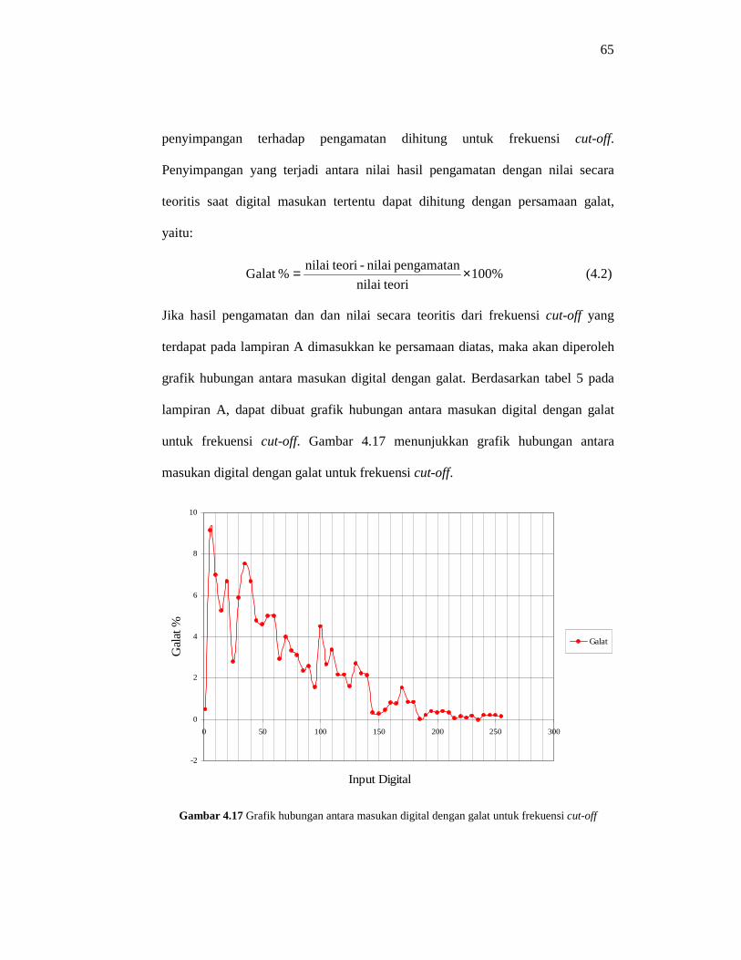
65
penyimpangan terhadap pengamatan dihitung untuk frekuensi cut-off.
Penyimpangan yang terjadi antara nilai hasil pengamatan dengan nilai secara
teoritis saat digital masukan tertentu dapat dihitung dengan persamaan galat,
yaitu:
%100 teorinilai
pengamatan nilai - teorinilai%Galat ×= (4.2)
Jika hasil pengamatan dan dan nilai secara teoritis dari frekuensi cut-off yang
terdapat pada lampiran A dimasukkan ke persamaan diatas, maka akan diperoleh
grafik hubungan antara masukan digital dengan galat. Berdasarkan tabel 5 pada
lampiran A, dapat dibuat grafik hubungan antara masukan digital dengan galat
untuk frekuensi cut-off. Gambar 4.17 menunjukkan grafik hubungan antara
masukan digital dengan galat untuk frekuensi cut-off.
-2
0
2
4
6
8
10
0 50 100 150 200 250 300
Input Digital
Gal
at %
Galat
Gambar 4.17 Grafik hubungan antara masukan digital dengan galat untuk frekuensi cut-off

66
Berdasarkan gambar 4.8, terlihat bahwa nilai galat tertinggi adalah sebesar 9,16 %
dan nilai galat terendah adalah sebesar 0,016 %. Nilai rata-rata galat untuk
frekuensi cut-off adalah sebesar 2,36 %.
4.4. Hubungan Antara Tegangan Referensi dengan Tegangan
Keluaran Pengali
Sub bab ini bertujuan untuk mengetahui apakah tegangan keluaran yang
dihasilkan merupakan perkalian antara masukan digital dengan tegangan referensi
pengali. Masukan digital diperoleh dari 8 saklar, saat saklar tidak terhubung
ground untuk masukan bit 1 (high) dan saat saklar terhubung ground untuk
masukan bit 0 (low), sedangkan tegangan referensi, Vref diperoleh secara langsung
dari keluaran penguat beda tingkat pertama saat AFG dihubungkan ke masukan
filter. Untuk tegangan keluaran pengali, jika dianalisis maka tegangan tersebut
merupakan perkalian antara tegangan referensi pengali dengan nilai bit yang
dimasukkan, yang sesuai dengan persamaan (2.29).
Sebagai contoh, jika di masukkan bit 125(d), terukur nilai tegangan
referensi sebesar 5,12 Vp-p, maka tegangan keluaran pengali diperoleh nilai
sebesar 2,6 Vp-p. Jika dibandingkan dengan dengan hasil secara teoritis, maka
tegangan keluaran pengali sebesar :
ppout VV −×= 12,5256
125

67
ppout VV −= 5,2
Berdasarkan tabel 7 pada lampiran B, dapat dibuat grafik hubungan
antara masukan digital dengan tegangan referensi dan tegangan keluaran pengali.
Gambar 4.18 menunjukkan grafik hubungan antara masukan digital dengan
tegangan referensi dan tegangan keluaran pengali.
0
0,2
0,4
0,6
0,8
1
1,2
0 50 100 150 200 250 300
Input Digital
Teg
anga
n R
efer
ensi/T
egan
gan
Out
put
Tegangan Referensi terhadap Tegangan Output (Pengamatan)
Tegangan Referensi terhadap Tegangan Output (Teori)
Gambar 4.18 Grafik hubungan antara masukan digital dengan tegangan referensi dan keluaran
pengali
Jika hasil pengamatan dan dan nilai secara teoritis dari tegangan keluaran pengali
yang terdapat pada lampiran B dimasukkan ke persamaan (4.2), maka akan
diperoleh grafik hubungan antara masukan digital dengan galat. Berdasarkan tabel
7 yang terdapat pada lampiran B, grafik hubungan antara masukan digital dengan
galat untuk tegangan keluaran pengali terhadap tegangan referensi yang
ditunjukkan oleh gambar 4.19

68
0
2
4
6
8
10
12
14
0 50 100 150 200 250 300
Input Digital
Gal
at %
Galat
Gambar 4.19 Grafik hubungan antara masukan digital dengan galat untuk tegangan keluaran
pengali
Berdasarkan gambar 4.19, nilai galat tertinggi adalah sebesar 12,820 % dan nilai
galat terendah adalah sebesar 0,358 %. Nilai rata-rata galat pada tegangan
keluaran terhadap tegangan referensi pengali adalah sebesar 3,20 %.

69
BAB V
KESIMPULAN DAN SARAN
1. Kesimpulan
Berdasarkan alat yang sudah dibuat dan dari data hasil pengamatan,
maka dapat disimpulkan sebagai berikut :
1. Alat ini dapat mengendalikan frekuensi cut-off untuk jangkauan frekuensi
cut off dari urutan rendah (urutan ke 1(fc=100 Hz)) sampai urutan tinggi
(urutan ke 255 (fc=255 Hz)) dari Filter Pelewat Rendah (Low Pass Filter)
dengan baik melalui input digital dari delapan saklar.
2. Semakin besar masukan digital maka pada tanggapan magnitude
perubahan frekuensi cut-off semakin ke arah frekuensi cut-off yang lebih
tinggi.
3. Pada percobaan untuk mengetahui hubungan masukan digital dan frekuensi
cut-off, untuk masukan digital dengan kenaikan setiap lima bit, pergeseran
frekuensi cut-off dari urutan rendah sampai urutan tinggi mengalami
kesalahan sebesar 0,342 % dari perhitungan secara teoritis. Nilai galat
tertinggi yaitu sebesar 9,16 % dan nilai galat terendah adalah sebesar 0,016
%.
4. Pada penaksiran nilai roll-off pada tanggapan magnitude pengamatan untuk
urutan rendah, urutan sedang dan urutan tinggi terjadi kesalahan sebesar
1,16 % dari perhitungan secara teoritis.
70
2. Saran
Alat ini masih dapat dikembangkan, untuk input digital, dapat memakai
counter dan untuk penampil dapat menggunakan tampilan seven segment dapat
berupa penampil bilangan desimal atau bilangan heksa. Untuk jenis filter dapat
dikembangkan dengan menggunakan jenis Filter Pelewat Jalur (Band Pass Filter),
Filter Pelewat Tinggi (High Pass Filter) dan Filter Penolak Jalur (Band Stop
Filter).
71
DAFTAR PUSTAKA
Boylestad, Robert, Nashelsky, Louis, 1996, Electronic Devices And Circuit Theory, Prentice-Hall, Inc., New Jersey. Putra, Afgianto Eko, 2002, Penapis Aktif Elektronika : Teori dan Praktek, C.V. Gava Media, Yogyakarta. Valkenburg, VME., 1982, Analog Filter Design, CBS College Publishing, New York. Irvine, Robert G., 1994, Operational Amplifier Characteristics And Applications, Prentice Hall, Inc., New Jersey.

LAMPIRAN

LAMPIRAN A
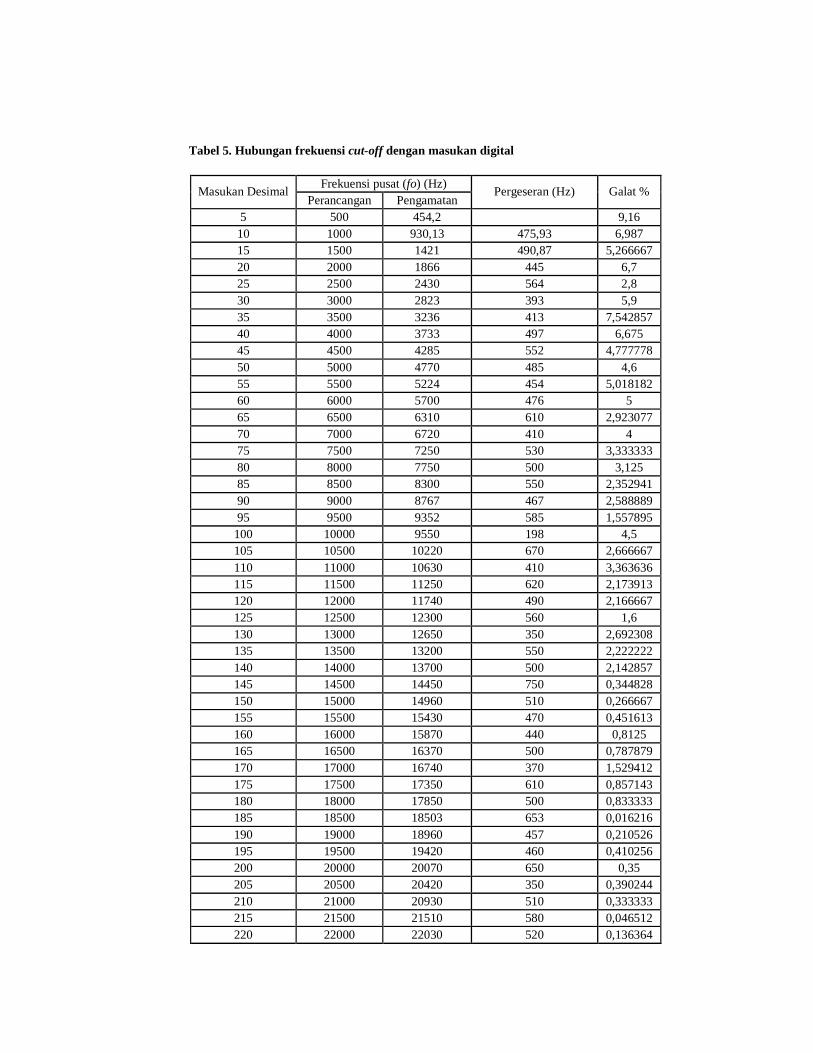
Tabel 5. Hubungan frekuensi cut-off dengan masukan digital
Frekuensi pusat (fo) (Hz) Masukan Desimal
Perancangan Pengamatan Pergeseran (Hz) Galat %
5 500 454,2 9,16 10 1000 930,13 475,93 6,987 15 1500 1421 490,87 5,266667 20 2000 1866 445 6,7 25 2500 2430 564 2,8 30 3000 2823 393 5,9 35 3500 3236 413 7,542857 40 4000 3733 497 6,675 45 4500 4285 552 4,777778 50 5000 4770 485 4,6 55 5500 5224 454 5,018182 60 6000 5700 476 5 65 6500 6310 610 2,923077 70 7000 6720 410 4 75 7500 7250 530 3,333333 80 8000 7750 500 3,125 85 8500 8300 550 2,352941 90 9000 8767 467 2,588889 95 9500 9352 585 1,557895
100 10000 9550 198 4,5 105 10500 10220 670 2,666667 110 11000 10630 410 3,363636 115 11500 11250 620 2,173913 120 12000 11740 490 2,166667 125 12500 12300 560 1,6 130 13000 12650 350 2,692308 135 13500 13200 550 2,222222 140 14000 13700 500 2,142857 145 14500 14450 750 0,344828 150 15000 14960 510 0,266667 155 15500 15430 470 0,451613 160 16000 15870 440 0,8125 165 16500 16370 500 0,787879 170 17000 16740 370 1,529412 175 17500 17350 610 0,857143 180 18000 17850 500 0,833333 185 18500 18503 653 0,016216 190 19000 18960 457 0,210526 195 19500 19420 460 0,410256 200 20000 20070 650 0,35 205 20500 20420 350 0,390244 210 21000 20930 510 0,333333 215 21500 21510 580 0,046512 220 22000 22030 520 0,136364

225 22500 22480 450 0,088889 230 23000 22960 480 0,173913 235 23500 23480 520 0,085106 240 24000 23950 470 0,208333 245 24500 24450 500 0,204082 250 25000 24950 500 0,2 255 25500 25510 590 0,156863

LAMPIRAN B

Tabel 6. Hubungan Input Digital dengan Tegangan Referensi dan Tegangan Output
Tegangan Output Digital Input
Ekuivalen Desimal
Tegangan Referensi Pengamatan Teori
00010100 20 5 0,44 0,39 00011001 25 5,2 0,52 0,507 00011110 30 5,2 0,68 0,609 00011110 35 5,28 0,76 0,721 00101000 40 5,28 0,84 0,825 00101101 45 5,04 0,96 0,885 00110010 50 5,04 1,08 0,984 00110111 55 5,04 1,16 1,082 00111100 60 5,04 1,24 1,181 01000001 65 5,12 1,36 1,3 01000110 70 5,04 1,44 1,378 01001011 75 5,04 1,56 1,476 01010000 80 5,04 1,64 1,575 01010101 85 5,12 1,76 1,7 01011010 90 5,04 1,84 1,771 01011111 95 5,04 1,96 1,87 01100100 100 5,04 2,04 1,968 01101001 105 5,04 2,12 2,067 01101110 110 5,04 2,24 2,165 01110011 115 5,04 2,32 2,264 01111000 120 5,28 2,56 2,475 01111101 125 5,12 2,6 2,5 10000010 130 5,2 2,72 2,64 10000111 135 4,96 2,72 2,615 10001100 140 4,96 2,8 2,712 10010001 145 4,96 2,84 2,809 10010110 150 4,96 2,92 2,906 10011011 155 4,96 3,04 3,003 10100000 160 4,88 3,12 3,05 10100101 165 4,8 3,12 3,093 10101010 170 4,8 3,24 3,187 10101111 175 4,8 3,32 3,281 10110100 180 4,8 3,4 3,375 10111001 185 4,72 3,48 3,41 10111110 190 4,64 3,52 3,443 11000011 195 4,64 3,56 3,534 11001000 200 4,56 3,64 3,562 11001101 205 4,48 3,68 3,587 11010010 210 4,48 3,72 3,675 11010111 215 4,4 3,76 3,695 11011100 220 4,4 3,84 3,781 11100001 225 4,32 3,84 3,796 11100110 230 4,24 3,84 3,809 11101011 235 4,24 3,92 3,892 11110000 240 4,08 3,84 3,825 11110110 245 4,08 3,92 3,904 11111010 250 4 3,92 3,906 11111111 255 3,92 3,92 3,904
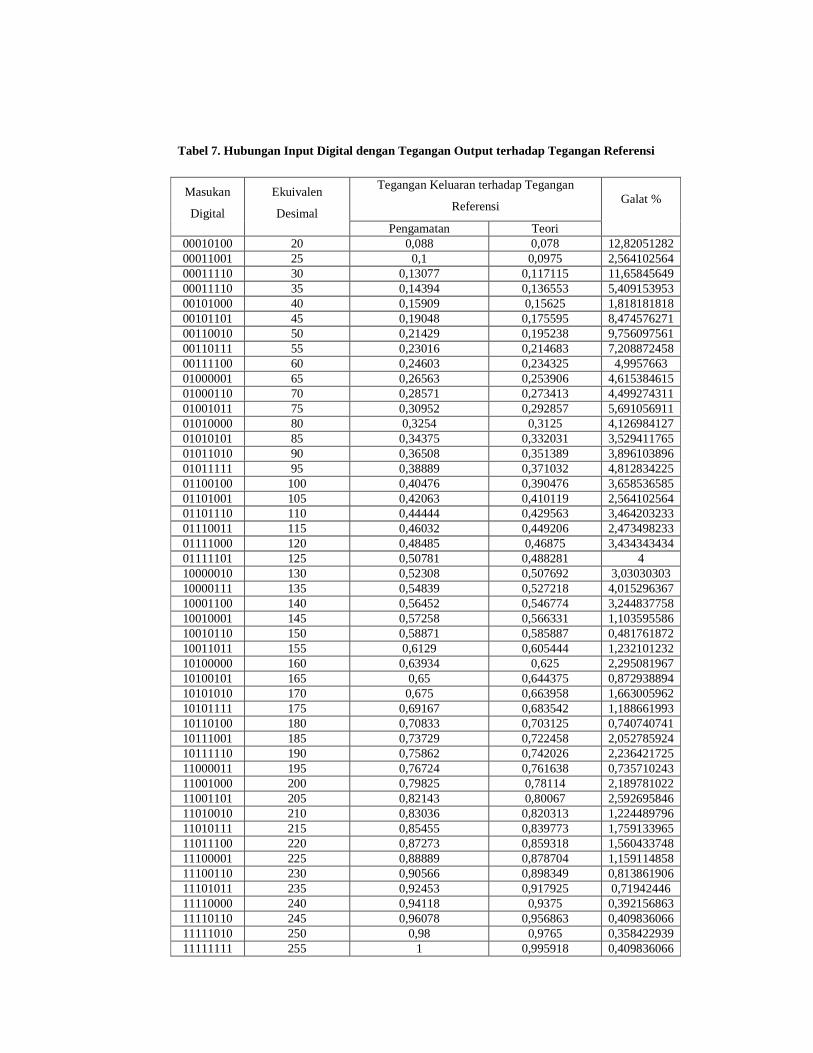
Tabel 7. Hubungan Input Digital dengan Tegangan Output terhadap Tegangan Referensi
Tegangan Keluaran terhadap Tegangan
Referensi Masukan
Digital
Ekuivalen
Desimal Pengamatan Teori
Galat %
00010100 20 0,088 0,078 12,82051282 00011001 25 0,1 0,0975 2,564102564 00011110 30 0,13077 0,117115 11,65845649 00011110 35 0,14394 0,136553 5,409153953 00101000 40 0,15909 0,15625 1,818181818 00101101 45 0,19048 0,175595 8,474576271 00110010 50 0,21429 0,195238 9,756097561 00110111 55 0,23016 0,214683 7,208872458 00111100 60 0,24603 0,234325 4,9957663 01000001 65 0,26563 0,253906 4,615384615 01000110 70 0,28571 0,273413 4,499274311 01001011 75 0,30952 0,292857 5,691056911 01010000 80 0,3254 0,3125 4,126984127 01010101 85 0,34375 0,332031 3,529411765 01011010 90 0,36508 0,351389 3,896103896 01011111 95 0,38889 0,371032 4,812834225 01100100 100 0,40476 0,390476 3,658536585 01101001 105 0,42063 0,410119 2,564102564 01101110 110 0,44444 0,429563 3,464203233 01110011 115 0,46032 0,449206 2,473498233 01111000 120 0,48485 0,46875 3,434343434 01111101 125 0,50781 0,488281 4 10000010 130 0,52308 0,507692 3,03030303 10000111 135 0,54839 0,527218 4,015296367 10001100 140 0,56452 0,546774 3,244837758 10010001 145 0,57258 0,566331 1,103595586 10010110 150 0,58871 0,585887 0,481761872 10011011 155 0,6129 0,605444 1,232101232 10100000 160 0,63934 0,625 2,295081967 10100101 165 0,65 0,644375 0,872938894 10101010 170 0,675 0,663958 1,663005962 10101111 175 0,69167 0,683542 1,188661993 10110100 180 0,70833 0,703125 0,740740741 10111001 185 0,73729 0,722458 2,052785924 10111110 190 0,75862 0,742026 2,236421725 11000011 195 0,76724 0,761638 0,735710243 11001000 200 0,79825 0,78114 2,189781022 11001101 205 0,82143 0,80067 2,592695846 11010010 210 0,83036 0,820313 1,224489796 11010111 215 0,85455 0,839773 1,759133965 11011100 220 0,87273 0,859318 1,560433748 11100001 225 0,88889 0,878704 1,159114858 11100110 230 0,90566 0,898349 0,813861906 11101011 235 0,92453 0,917925 0,71942446 11110000 240 0,94118 0,9375 0,392156863 11110110 245 0,96078 0,956863 0,409836066 11111010 250 0,98 0,9765 0,358422939 11111111 255 1 0,995918 0,409836066

LAMPIRAN C

Gambar Rangkaian Keseluruhan

LAMPIRAN D

Rangkaian Catu Daya

DAC0830/DAC08328-Bit µP Compatible, Double-Buffered D to A ConvertersGeneral DescriptionThe DAC0830 is an advanced CMOS/Si-Cr 8-bit multiplyingDAC designed to interface directly with the 8080, 8048,8085, Z80®, and other popular microprocessors. A depositedsilicon-chromium R-2R resistor ladder network divides thereference current and provides the circuit with excellent tem-perature tracking characteristics (0.05% of Full Scale Rangemaximum linearity error over temperature). The circuit usesCMOS current switches and control logic to achieve lowpower consumption and low output leakage current errors.Special circuitry provides TTL logic input voltage level com-patibility.
Double buffering allows these DACs to output a voltage cor-responding to one digital word while holding the next digitalword. This permits the simultaneous updating of any numberof DACs.
The DAC0830 series are the 8-bit members of a family ofmicroprocessor-compatible DACs (MICRO-DAC™).
Featuresn Double-buffered, single-buffered or flow-through digital
data inputsn Easy interchange and pin-compatible with 12-bit
DAC1230 seriesn Direct interface to all popular microprocessorsn Linearity specified with zero and full scale adjust
only — NOT BEST STRAIGHT LINE FIT.n Works with ±10V reference-full 4-quadrant multiplicationn Can be used in the voltage switching moden Logic inputs which meet TTL voltage level specs (1.4V
logic threshold)n Operates “STAND ALONE” (without µP) if desiredn Available in 20-pin small-outline or molded chip carrier
package
Key Specificationsn Current settling time: 1 µsn Resolution: 8 bitsn Linearity: 8, 9, or 10 bits (guaranteed over temp.)n Gain Tempco: 0.0002% FS/˚Cn Low power dissipation: 20 mWn Single power supply: 5 to 15 VDC
Typical Application
BI-FET™ and MICRO-DAC™ are trademarks of National Semiconductor Corporation.Z80® is a registered trademark of Zilog Corporation.
DS005608-1
May 1999
DA
C0830/D
AC
08328-B
itµPC
ompatible,D
ouble-Buffered
Dto
AC
onverters
© 1999 National Semiconductor Corporation DS005608 www.national.com

Connection Diagrams (Top Views)
Dual-In-Line andSmall-Outline Packages
DS005608-21
Molded Chip Carrier Package
DS005608-22
www.national.com 2

Absolute Maximum Ratings (Notes 1, 2)
If Military/Aerospace specified devices are required,please contact the National Semiconductor Sales Office/Distributors for availability and specifications.
Supply Voltage (VCC) 17 VDC
Voltage at Any Digital Input VCC to GNDVoltage at VREF Input ±25VStorage Temperature Range −65˚C to +150˚CPackage Dissipation
at TA=25˚C (Note 3) 500 mWDC Voltage Applied to
IOUT1 or IOUT2 (Note 4) −100 mV to VCC
ESD Susceptability (Note 4) 800V
Lead Temperature (Soldering, 10 sec.)Dual-In-Line Package (plastic) 260˚CDual-In-Line Package (ceramic) 300˚CSurface Mount Package
Vapor Phase (60 sec.) 215˚CInfrared (15 sec.) 220˚C
Operating ConditionsTemperature Range TMIN≤TA≤TMAX
Part numbers with “LCN” suffix 0˚C to +70˚CPart numbers with “LCWM” suffix 0˚C to +70˚CPart numbers with “LCV” suffix 0˚C to +70˚CPart numbers with “LCJ” suffix −40˚C to +85˚CPart numbers with “LJ” suffix −55˚C to +125˚C
Voltage at Any Digital Input VCC to GND
Electrical CharacteristicsVREF=10.000 VDC unless otherwise noted. Boldface limits apply over temperature, T MIN≤TA≤TMAX. For all other limitsTA=25˚C.
Parameter Conditions SeeNote
VCC = 4.75 VDCVCC = 15.75 VDC
VCC = 5 VDC ±5%VCC = 12 VDC ±5%
to 15 VDC ±5% LimitUnits
Typ(Note 12)
TestedLimit
(Note 5)
DesignLimit
(Note 6)
CONVERTER CHARACTERISTICS
Resolution 8 8 8 bits
Linearity Error Max Zero and full scale adjusted 4, 8
−10V≤VREF≤+10V
DAC0830LJ & LCJ 0.05 0.05 % FSR
DAC0832LJ & LCJ 0.2 0.2 % FSR
DAC0830LCN, LCWM &LCV
0.05 0.05 % FSR
DAC0831LCN 0.1 0.1 % FSR
DAC0832LCN, LCWM &LCV
0.2 0.2 % FSR
Differential Nonlinearity Zero and full scale adjusted 4, 8
Max −10V≤VREF≤+10V
DAC0830LJ & LCJ 0.1 0.1 % FSR
DAC0832LJ & LCJ 0.4 0.4 % FSR
DAC0830LCN, LCWM &LCV
0.1 0.1 % FSR
DAC0831LCN 0.2 0.2 % FSR
DAC0832LCN, LCWM &LCV
0.4 0.4 % FSR
Monotonicity −10V≤VREF LJ & LCJ 4 8 8 bits
≤+10V LCN, LCWM & LCV 8 8 bits
Gain Error Max Using Internal Rfb 7 ±0.2 ±1 ±1 % FS
−10V≤VREF≤+10V
Gain Error Tempco Max Using internal Rfb 0.0002 0.0006 %
FS/˚C
Power Supply Rejection All digital inputs latched high
VCC=14.5V to 15.5V 0.0002 0.0025 %
11.5V to 12.5V 0.0006 FSR/V
4.5V to 5.5V 0.013 0.015
Reference Max 15 20 20 kΩ
Input Min 15 10 10 kΩ
Output Feedthrough Error VREF=20 Vp-p, f=100 kHzAll data inputs latched low 3 mVp-p
www.national.com3

Electrical Characteristics (Continued)
VREF=10.000 VDC unless otherwise noted. Boldface limits apply over temperature, T MIN≤TA≤TMAX. For all other limitsTA=25˚C.
Parameter Conditions SeeNote
VCC = 4.75 VDCVCC = 15.75 VDC
VCC = 5 VDC ±5%VCC = 12 VDC ±5%
to 15 VDC ±5% LimitUnits
Typ(Note 12)
TestedLimit
(Note 5)
DesignLimit
(Note 6)
CONVERTER CHARACTERISTICS
Output LeakageCurrent Max
IOUT1 All data inputs LJ & LCJ 10 100 100 nA
latched low LCN, LCWM & LCV 50 100
IOUT2 All data inputs LJ & LCJ 100 100 nA
latched high LCN, LCWM & LCV 50 100
Output IOUT1 All data inputs 45 pF
Capacitance IOUT2 latched low 115
IOUT1 All data inputs 130 pF
IOUT2 latched high 30
DIGITAL AND DC CHARACTERISTICS
Digital Input Max Logic Low LJ: 4.75V 0.6
Voltages LJ: 15.75V 0.8
LCJ: 4.75V 0.7 VDC
LCJ: 15.75V 0.8
LCN, LCWM, LCV 0.95 0.8
Min Logic High LJ & LCJ 2.0 2.0 VDC
LCN, LCWM, LCV 1.9 2.0
Digital Input Max Digital inputs <0.8V
Currents LJ & LCJ −50 −200 −200 µA
LCN, LCWM, LCV −160 −200 µA
Digital inputs>2.0V
LJ & LCJ 0.1 +10 +10 µA
LCN, LCWM, LCV +8 +10
Supply Current Max LJ & LCJ 1.2 3.5 3.5 mA
Drain LCN, LCWM, LCV 1.7 2.0
Electrical CharacteristicsVREF=10.000 VDC unless otherwise noted. Boldface limits apply over temperature, T MIN≤TA≤TMAX. For all other limitsTA=25˚C.
Symbol Parameter Conditions SeeNote
VCC=15.75 VDCVCC=12 VDC±5%to 15 VDC ±5% VCC=4.75 VDC
VCC=5VDC±5%
LimitUnitsTyp
(Note 12)
TestedLimit
(Note 5)
Design Limit(Note 6)
Typ(Note 12)
TestedLimit
(Note 5)
DesignLimit
(Note 6)
AC CHARACTERISTICS
ts Current Setting VIL=0V, VIH=5V 1.0 1.0 µs
Time
tW Write and XFER VIL=0V, VIH=5V 11 100 250 375 600
Pulse Width Min 9 320 320 900 900
tDS Data Setup Time VIL=0V, VIH=5V 9 100 250 375 600
Min 320 320 900 900
tDH Data Hold Time VIL=0V, VIH=5V 9 30 50 ns
Min 30 50
tCS Control Setup Time VIL=0V, VIH=5V 9 110 250 600 900
Min 320 320 1100 1100
tCH Control Hold Time VIL=0V, VIH=5V 9 0 0 10 0 0
Min 0 0
Note 1: Absolute Maximum Ratings indicate limits beyond which damage to the device may occur. DC and AC electrical specifications do not apply when operatingthe device beyond its specified operating conditions.
Note 2: All voltages are measured with respect to GND, unless otherwise specified.
www.national.com 4

Electrical Characteristics (Continued)
Note 3: The maximum power dissipation must be derated at elevated temperatures and is dictated by TJMAX, θJA, and the ambient temperature, TA. The maximumallowable power dissipation at any temperature is PD = (TJMAX − TA)/θJA or the number given in the Absolute Maximum Ratings, whichever is lower. For this device,TJMAX = 125˚C (plastic) or 150˚C (ceramic), and the typical junction-to-ambient thermal resistance of the J package when board mounted is 80˚C/W. For the N pack-age, this number increases to 100˚C/W and for the V package this number is 120˚C/W.
Note 4: For current switching applications, both IOUT1 and IOUT2 must go to ground or the “Virtual Ground” of an operational amplifier. The linearity error is degradedby approximately VOS ÷ VREF. For example, if VREF = 10V then a 1 mV offset, VOS, on IOUT1 or IOUT2 will introduce an additional 0.01% linearity error.
Note 5: Tested limits are guaranteed to National’s AOQL (Average Outgoing Quality Level).
Note 6: Guaranteed, but not 100% production tested. These limits are not used to calculate outgoing quality levels.
Note 7: Guaranteed at VREF=±10 VDC and VREF=±1 VDC.
Note 8: The unit “FSR” stands for “Full Scale Range.” “Linearity Error” and “Power Supply Rejection” specs are based on this unit to eliminate dependence on a par-ticular VREF value and to indicate the true performance of the part. The “Linearity Error” specification of the DAC0830 is “0.05% of FSR (MAX)”. This guarantees thatafter performing a zero and full scale adjustment (see Sections 2.5 and 2.6), the plot of the 256 analog voltage outputs will each be within 0.05%xVREF of a straightline which passes through zero and full scale.
Note 9: Boldface tested limits apply to the LJ and LCJ suffix parts only.
Note 10: A 100nA leakage current with Rfb=20k and VREF=10V corresponds to a zero error of (100x10−9x20x103)x100/10 which is 0.02% of FS.
Note 11: The entire write pulse must occur within the valid data interval for the specified tW, tDS, tDH, and tS to apply.
Note 12: Typicals are at 25˚C and represent most likely parametric norm.
Note 13: Human body model, 100 pF discharged through a 1.5 kΩ resistor.
Switching Waveform
DS005608-2
www.national.com5

Definition of Package Pinouts
Control Signals (All control signals level actuated)
CS: Chip Select (active low). The CS in combinationwith ILE will enable WR1.
ILE: Input Latch Enable (active high). The ILE in combi-nation with CS enables WR1.
WR1: Write 1. The active low WR1 is used to load the digi-tal input data bits (DI) into the input latch. The datain the input latch is latched when WR1 is high. Toupdate the input latch–CS and WR1 must be lowwhile ILE is high.
WR2: Write 2 (active low). This signal, in combination withXFER, causes the 8-bit data which is available inthe input latch to transfer to the DAC register.
XFER: Transfer control signal (active low). The XFER willenable WR2.
Other Pin Functions
DI0-DI7: Digital Inputs. DI0 is the least significant bit (LSB)and DI7 is the most significant bit (MSB).
IOUT1: DAC Current Output 1. IOUT1 is a maximum for adigital code of all 1’s in the DAC register, and iszero for all 0’s in DAC register.
IOUT2: DAC Current Output 2. IOUT2 is a constant minusIOUT1 , or IOUT1 + IOUT2 = constant (I full scale fora fixed reference voltage).
Rfb: Feedback Resistor. The feedback resistor is pro-
vided on the IC chip for use as the shunt feedbackresistor for the external op amp which is used toprovide an output voltage for the DAC. This on-chip resistor should always be used (not an exter-nal resistor) since it matches the resistors whichare used in the on-chip R-2R ladder and tracksthese resistors over temperature.
VREF: Reference Voltage Input. This input connects anexternal precision voltage source to the internalR-2R ladder. VREF can be selected over the rangeof +10 to −10V. This is also the analog voltage in-put for a 4-quadrant multiplying DAC application.
VCC: Digital Supply Voltage . This is the power supplypin for the part. VCC can be from +5 to +15VDC.Operation is optimum for +15VDC
GND: The pin 10 voltage must be at the same groundpotential as IOUT1 and IOUT2 for current switchingapplications. Any difference of potential (VOS pin10) will result in a linearity change of
For example, if VREF = 10V and pin 10 is 9mV offset fromIOUT1 and IOUT2 the linearity change will be 0.03%.
Pin 3 can be offset ±100mV with no linearity change, but thelogic input threshold will shift.
Linearity Error
Definition of TermsResolution: Resolution is directly related to the number ofswitches or bits within the DAC. For example, the DAC0830has 28 or 256 steps and therefore has 8-bit resolution.
Linearity Error: Linearity Error is the maximum deviationfrom a straight line passing through the endpoints of theDAC transfer characteristic. It is measured after adjusting forzero and full-scale. Linearity error is a parameter intrinsic tothe device and cannot be externally adjusted.
National’s linearity “end point test” (a) and the “best straightline” test (b,c) used by other suppliers are illustrated above.The “end point test’’ greatly simplifies the adjustment proce-dure by eliminating the need for multiple iterations of check-ing the linearity and then adjusting full scale until the linearityis met. The “end point test’’ guarantees that linearity is metafter a single full scale adjust. (One adjustment vs. multiple
iterations of the adjustment.) The “end point test’’ uses astandard zero and F.S. adjustment procedure and is a muchmore stringent test for DAC linearity.
Power Supply Sensitivity: Power supply sensitivity is ameasure of the effect of power supply changes on the DACfull-scale output.
Settling Time: Settling time is the time required from a codetransition until the DAC output reaches within ±1⁄2LSB of thefinal output value. Full-scale settling time requires a zero tofull-scale or full-scale to zero output change.
Full Scale Error: Full scale error is a measure of the outputerror between an ideal DAC and the actual device output.Ideally, for the DAC0830 series, full scale is VREF −1LSB.For VREF = 10V and unipolar operation, VFULL-SCALE =10,0000V–39mV 9.961V. Full-scale error is adjustable tozero.
DS005608-23
a) End point test afterzero and fs adj.
DS005608-24
b) Best straight line DS005608-25
c) Shifting fs adj. to passbest straight line test
www.national.com 6

Definition of Terms (Continued)
Differential Nonlinearity: The difference between any twoconsecutive codes in the transfer curve from the theoretical1 LSB to differential nonlinearity.
Monotonic: If the output of a DAC increases for increasingdigital input code, then the DAC is monotonic. An 8-bit DACwhich is monotonic to 8 bits simply means that increasingdigital input codes will produce an increasing analog output.
Typical Performance Characteristics
DS005608-4
FIGURE 1. DAC0830 Functional Diagram
Digital Input Thresholdvs. Temperature
DS005608-26
Digital Input Thresholdvs. VCC
DS005608-27
Gain and Linearity ErrorVariation vs. Temperature
DS005608-28
www.national.com7

Typical Performance Characteristics (Continued)
DAC0830 Series Application HintsThese DAC’s are the industry’s first microprocessor compat-ible, double-buffered 8-bit multiplying D to A converters.Double-buffering allows the utmost application flexibility froma digital control point of view. This 20-pin device is also pinfor pin compatible (with one exception) with the DAC1230, a12-bit MICRO-DAC. In the event that a system’s analog out-put resolution and accuracy must be upgraded, substitutingthe DAC1230 can be easily accomplished. By tying addressbit A0 to the ILE pin, a two-byte µP write instruction (doubleprecision) which automatically increments the address forthe second byte write (starting with A0=“1”) can be used.This allows either an 8-bit or the 12-bit part to be used withno hardware or software changes. For the simplest 8-bit ap-plication, this pin should be tied to VCC (also see other usesin section 1.1).
Analog signal control versatility is provided by a precisionR-2R ladder network which allows full 4-quadrant multiplica-tion of a wide range bipolar reference voltage by an applieddigital word.
1.0 DIGITAL CONSIDERATIONS
A most unique characteristic of these DAC’s is that the 8-bitdigital input byte is double-buffered. This means that thedata must transfer through two independently controlled 8-bitlatching registers before being applied to the R-2R laddernetwork to change the analog output. The addition of a sec-ond register allows two useful control features. First, anyDAC in a system can simultaneously hold the current DACdata in one register (DAC register) and the next data word inthe second register (input register) to allow fast updating ofthe DAC output on demand. Second, and probably more im-portant, double-buffering allows any number of DAC’s in asystem to be updated to their new analog output levels si-multaneously via a common strobe signal.
The timing requirements and logic level convention of theregister control signals have been designed to minimize oreliminate external interfacing logic when applied to mostpopular microprocessors and development systems. It iseasy to think of these converters as 8-bit “write-only”memory locations that provide an analog output quantity. Allinputs to these DAC’s meet TTL voltage level specs and canalso be driven directly with high voltage CMOS logic innon-microprocessor based systems. To prevent damage tothe chip from static discharge, all unused digital inputsshould be tied to VCC or ground. If any of the digital inputsare inadvertantly left floating, the DAC interprets the pin as alogic “1”.
1.1 Double-Buffered Operation
Updating the analog output of these DAC’s in adouble-buffered manner is basically a two step or doublewrite operation. In a microprocessor system two unique sys-tem addresses must be decoded, one for the input latch con-trolled by the CS pin and a second for the DAC latch whichis controlled by the XFER line. If more than one DAC is beingdriven, Figure 2, the CS line of each DAC would typically bedecoded individually, but all of the converters could share acommon XFER address to allow simultaneous updating ofany number of DAC’s. The timing for this operation is shown,Figure 3.
It is important to note that the analog outputs that will changeafter a simultaneous transfer are those from the DAC’swhose input register had been modified prior to the XFERcommand.
Gain and Linearity ErrorVariation vs. Supply Voltage
DS005608-29
Write Pulse Width
DS005608-30
Data Hold Time
DS005608-31
www.national.com 8

DAC0830 Series Application Hints (Continued)
The ILE pin is an active high chip select which can be de-coded from the address bus as a qualifier for the normal CSsignal generated during a write operation. This can be usedto provide a higher degree of decoding unique control sig-nals for a particular DAC, and thereby create a more efficientaddressing scheme.
Another useful application of the ILE pin of each DAC in amultiple DAC system is to tie these inputs together and usethis as a control line that can effectively “freeze” the outputsof all the DAC’s at their present value. Pulling this line lowlatches the input register and prevents new data from beingwritten to the DAC. This can be particularly useful in multi-processing systems to allow a processor other than the one
controlling the DAC’s to take over control of the data bus andcontrol lines. If this second system were to use the same ad-dresses as those decoded for DAC control (but for a differentpurpose) the ILE function would prevent the DAC’s from be-ing erroneously altered.
In a “Stand-Alone” system the control signals are generatedby discrete logic. In this case double-buffering can be con-trolled by simply taking CS and XFER to a logic “0”, ILE to alogic “1” and pulling WR1 low to load data to the input latch.Pulling WR2 low will then update the analog output. A logic“1” on either of these lines will prevent the changing of theanalog output.
DS005608-35
*TIE TO LOGIC 1 IF NOT NEEDED (SEE SEC. 1.1).
FIGURE 2. Controlling Mutiple DACs
DS005608-36
FIGURE 3.
www.national.com9

DAC0830 Series Application Hints (Continued)
1.2 Single-Buffered Operation
In a microprocessor controlled system where maximum datathroughput to the DAC is of primary concern, or when onlyone DAC of several needs to be updated at a time, asingle-buffered configuration can be used. One of the two in-ternal registers allows the data to flow through and the otherregister will serve as the data latch.
Digital signal feedthrough (see Section 1.5) is minimized ifthe input register is used as the data latch. Timing for thismode is shown in Figure 4.
Single-buffering in a “stand-alone” system is achieved bystrobing WR1 low to update the DAC with CS, WR2 andXFER grounded and ILE tied high.
1.3 Flow-Through Operation
Though primarily designed to provide microprocessor inter-face compatibility, the MICRO-DAC’s can easily be config-ured to allow the analog output to continuously reflect thestate of an applied digital input. This is most useful in appli-cations where the DAC is used in a continuous feedbackcontrol loop and is driven by a binary up-down counter, or infunction generation circuits where a ROM is continuouslyproviding DAC data.
Simply grounding CS, WR1, WR2, and XFER and tying ILEhigh allows both internal registers to follow the applied digitalinputs (flow-through) and directly affect the DAC analog out-put.
1.4 Control Signal Timing
When interfacing these MICRO-DAC to any microprocessor,there are two important time relationships that must be con-sidered to insure proper operation. The first is the minimumWR strobe pulse width which is specified as 900 ns for allvalid operating conditions of supply voltage and ambienttemperature, but typically a pulse width of only 180ns is ad-equate if VCC=15VDC. A second consideration is that theguaranteed minimum data hold time of 50ns should be met
or erroneous data can be latched. This hold time is definedas the length of time data must be held valid on the digital in-puts after a qualified (via CS) WR strobe makes a low to hightransition to latch the applied data.
If the controlling device or system does not inherently meetthese timing specs the DAC can be treated as a slowmemory or peripheral and utilize a technique to extend thewrite strobe. A simple extension of the write time, by addinga wait state, can simultaneously hold the write strobe activeand data valid on the bus to satisfy the minimum WR pulse-width. If this does not provide a sufficient data hold time atthe end of the write cycle, a negative edge triggeredone-shot can be included between the system write strobeand the WR pin of the DAC. This is illustrated in Figure 5 foran exemplary system which provides a 250ns WR strobetime with a data hold time of less than 10ns.
The proper data set-up time prior to the latching edge (LO toHI transition) of the WR strobe, is insured if the WR pulse-width is within spec and the data is valid on the bus for theduration of the DAC WR strobe.
1.5 Digital Signal Feedthrough
When data is latched in the internal registers, but the digitalinputs are changing state, a narrow spike of current may flowout of the current output terminals. This spike is caused bythe rapid switching of internal logic gates that are respondingto the input changes.
There are several recommendations to minimize this effect.When latching data in the DAC, always use the input registeras the latch. Second, reducing the VCC supply for the DACfrom +15V to +5V offers a factor of 5 improvement in themagnitude of the feedthrough, but at the expense of internallogic switching speed. Finally, increasing CC (Figure 8) to avalue consistent with the actual circuit bandwidth require-ments can provide a substantial damping effect on any out-put spikes.
DS005608-7
ILE=LOGIC “1”; WR2 and XFER GROUNDED
FIGURE 4.
www.national.com 10

DAC0830 Series Application Hints (Continued)
2.0 ANALOG CONSIDERATIONS
The fundamental purpose of any D to A converter is to pro-vide an accurate analog output quantity which is representa-tive of the applied digital word. In the case of the DAC0830,the output, IOUT1, is a current directly proportional to theproduct of the applied reference voltage and the digital inputword. For application versatility, a second output, IOUT2, isprovided as a current directly proportional to the complementof the digital input. Basically:
where the digital input is the decimal (base 10) equivalent ofthe applied 8-bit binary word (0 to 255), VREF is the voltageat pin 8 and 15 kΩ is the nominal value of the internal resis-tance, R, of the R-2R ladder network (discussed in Section2.1).
Several factors external to the DAC itself must be consid-ered to maintain analog accuracy and are covered in subse-quent sections.
2.1 The Current Switching R-2R Ladder
The analog circuitry, Figure 6, consists of a silicon-chromium(SiCr or Si-chrome) thin film R-2R ladder which is depositedon the surface oxide of the monolithic chip. As a result, thereare no parasitic diode problems with the ladder (as theremay be with diffused resistors) so the reference voltage,VREF, can range −10V to +10V even if VCC for the device is5VDC.
The digital input code to the DAC simply controls the positionof the SPDT current switches and steers the available laddercurrent to either IOUT1 or IOUT2 as determined by the logic in-
put level (“1” or “0”) respectively, as shown in Figure 6. TheMOS switches operate in the current mode with a small volt-age drop across them and can therefore switch currents ofeither polarity. This is the basis for the 4-quadrant multiplyingfeature of this DAC.
2.2 Basic Unipolar Output Voltage
To maintain linearity of output current with changes in the ap-plied digital code, it is important that the voltages at both ofthe current output pins be as near ground potential (0VDC)as possible. With VREF=+10V every millivolt appearing at ei-ther IOUT1 or IOUT2 will cause a 0.01% linearity error. In mostapplications this output current is converted to a voltage byusing an op amp as shown in Figure 7.
The inverting input of the op amp is a “virtual ground” createdby the feedback from its output through the internal 15 kΩ re-sistor, Rfb. All of the output current (determined by the digitalinput and the reference voltage) will flow through Rfb to theoutput of the amplifier. Two-quadrant operation can be ob-tained by reversing the polarity of VREF thus causing IOUT1 toflow into the DAC and be sourced from the output of the am-plifier. The output voltage, in either case, is always equal toIOUT1xRfb and is the opposite polarity of the reference volt-age.
The reference can be either a stable DC voltage source oran AC signal anywhere in the range from −10V to +10V. TheDAC can be thought of as a digitally controlled attenuator:the output voltage is always less than or equal to the appliedreference voltage. The VREF terminal of the device presentsa nominal impedance of 15 kΩ to ground to external circuitry.
Always use the internal Rfb resistor to create an output volt-age since this resistor matches (and tracks with tempera-ture) the value of the resistors used to generate the outputcurrent (IOUT1).
DS005608-8
FIGURE 5. Accommodating a High Speed System
www.national.com11

DAC0830 Series Application Hints (Continued)
2.3 Op Amp Considerations
The op amp used in Figure 7 should have offset voltage null-ing capability (See Section 2.5).
The selected op amp should have as low a value of inputbias current as possible. The product of the bias currenttimes the feedback resistance creates an output voltage er-ror which can be significant in low reference voltage applica-tions. BI-FET™ op amps are highly recommended for usewith these DACs because of their very low input current.
Transient response and settling time of the op amp are im-portant in fast data throughput applications. The largest sta-bility problem is the feedback pole created by the feedbackresistance, Rfb, and the output capacitance of the DAC. Thisappears from the op amp output to the (−) input and includesthe stray capacitance at this node. Addition of a lead capaci-tance, CC in Figure 8, greatly reduces overshoot and ringingat the output for a step change in DAC output current.
Finally, the output voltage swing of the amplifier must begreater than VREF to allow reaching the full scale output volt-age. Depending on the loading on the output of the amplifierand the available op amp supply voltages (only ±12 volts inmany development systems), a reference voltage less than10 volts may be necessary to obtain the full analog outputvoltage range.
2.4 Bipolar Output Voltage with a Fixed Reference
The addition of a second op amp to the previous circuitry canbe used to generate a bipolar output voltage from a fixed ref-erence voltage. This, in effect, gives sign significance to theMSB of the digital input word and allows two-quadrant multi-plication of the reference voltage. The polarity of the refer-ence can also be reversed to realize full 4-quadrant multipli-cation: ±VREFx±Digital Code=±VOUT. This circuit is shownin Figure 9.
This configuration features several improvements over exist-ing circuits for bipolar outputs with other multiplying DACs.Only the offset voltage of amplifier 1 has to be nulled to pre-serve linearity of the DAC. The offset voltage error of thesecond op amp (although a constant output voltage error)has no effect on linearity. It should be nulled only if absoluteoutput accuracy is required. Finally, the values of the resis-tors around the second amplifier do not have to match the in-ternal DAC resistors, they need only to match and tempera-ture track each other. A thin film 4-resistor network availablefrom Beckman Instruments, Inc. (part no. 694-3-R10K-D) isideally suited for this application. These resistors arematched to 0.1% and exhibit only 5 ppm/˚C resistance track-ing temperature coefficient. Two of the four available 10 kΩresistors can be paralleled to form R in Figure 9 and theother two can be used independently as the resistances la-beled 2R.
2.5 Zero Adjustment
For accurate conversions, the input offset voltage of the out-put amplifier must always be nulled. Amplifier offset errorscreate an overall degradation of DAC linearity.
The fundamental purpose of zeroing is to make the voltageappearing at the DAC outputs as near 0VDC as possible.This is accomplished for the typical DAC — op amp connec-tion (Figure 7) by shorting out Rfb, the amplifier feedback re-sistor, and adjusting the VOS nulling potentiometer of the opamp until the output reads zero volts. This is done, of course,with an applied digital code of all zeros if IOUT1 is driving theop amp (all one’s for IOUT2). The short around Rfb is then re-moved and the converter is zero adjusted.
DS005608-37
FIGURE 6.
DS005608-38
FIGURE 7.
www.national.com 12

DAC0830 Series Application Hints (Continued)
2.6 Full-Scale Adjustment
In the case where the matching of Rfb to the R value of theR-2R ladder (typically ±0.2%) is insufficient for full-scale ac-curacy in a particular application, the VREF voltage can beadjusted or an external resistor and potentiometer can beadded as shown in Figure 10 to provide a full-scale adjust-ment.
The temperature coefficients of the resistors used for this ad-justment are of an important concern. To prevent degrada-tion of the gain error temperature coefficient by the external
resistors, their temperature coefficients ideally would have tomatch that of the internal DAC resistors, which is a highly im-practical constraint. For the values shown in Figure 10, if theresistor and the potentiometer each had a temperature coef-ficient of ±100 ppm/˚C maximum, the overall gain error tem-perature coefficent would be degraded a maximum of0.0025%/˚C for an adjustment pot setting of less than 3% ofRfb.
DS005608-39
tsOP Amp C C (O to Full Scale)
LF356 22 pF 4 µs
LF351 22 pF 5 µs
LF357* 10 pF 2 µs
*2.4 kΩ RESISTOR ADDED FROM−INPUT TO GROUND TOINSURE STABILITY
FIGURE 8.
DS005608-40
Input Code IDEAL V OUT
MSB LSB +V REF −VREF
1 1 1 1 1 1 1 1
1 1 0 0 0 0 0 0
1 0 0 0 0 0 0 0
0 1 1 1 1 1 1 1
0 0 1 1 1 1 1 1
0 0 0 0 0 0 0 0
*THESE RESISTORS ARE AVAILABLE FROM BECKMAN INSTRUMENTS, INC. AS THEIR PART NO. 694-3-R10K-D
FIGURE 9.
www.national.com13

DAC0830 Series Application Hints(Continued)
2.7 Using the DAC0830 in a Voltage SwitchingConfiguration
The R-2R ladder can also be operated as a voltage switch-ing network. In this mode the ladder is used in an invertedmanner from the standard current switching configuration.
The reference voltage is connected to one of the current out-put terminals (IOUT1 for true binary digital control, IOUT2 is forcomplementary binary) and the output voltage is taken fromthe normal VREF pin. The converter output is now a voltagein the range from 0V to 255/256 VREF as a function of the ap-plied digital code as shown in Figure 11.
This configuration offers several useful application advan-tages. Since the output is a voltage, an external op amp isnot necessarily required but the output impedance of theDAC is fairly high (equal to the specified reference input re-sistance of 10 kΩ to 20 kΩ) so an op amp may be used forbuffering purposes. Some of the advantages of this modeare illustrated in Figures 12, 13, 14, 15.
There are two important things to keep in mind when usingthis DAC in the voltage switching mode. The applied refer-ence voltage must be positive since there are internal para-sitic diodes from ground to the IOUT1 and IOUT2 terminalswhich would turn on if the applied reference went negative.There is also a dependence of conversion linearity and gainerror on the voltage difference between VCC and the voltageapplied to the normal current output terminals. This is a re-sult of the voltage drive requirements of the ladder switches.To ensure that all 8 switches turn on sufficiently (so as not toadd significant resistance to any leg of the ladder andthereby introduce additional linearity and gain errors) it isrecommended that the applied reference voltage be keptless than +5VDC and VCC be at least 9V more positive thanVREF. These restrictions ensure less than 0.1% linearity andgain error change. Figures 16, 17, 18 characterize the ef-fects of bringing VREF and VCC closer together as well astypical temperature performance of this voltage switchingconfiguration.
DS005608-11
FIGURE 10. Adding Full-Scale Adjustment
DS005608-12
FIGURE 11. Voltage Mode Switching
DS005608-41
• Voltage switching mode eliminates output signal inver-sion and therefore a need for a negative power supply.
• Zero code output voltage is limited by the low level outputsaturation voltage of the op amp. The 2 kΩ pull-down re-sistor helps to reduce this voltage.
• VOS of the op amp has no effect on DAC linearity.
FIGURE 12. Single Supply DAC
www.national.com 14

DAC0830 Series Application Hints (Continued)
DS005608-42
FIGURE 13. Obtaining a Bipolar Output from a FixedReference with a Single Op Amp
DS005608-60
FIGURE 14. Bipolar Output with Increased Output Voltage Swing
www.national.com15
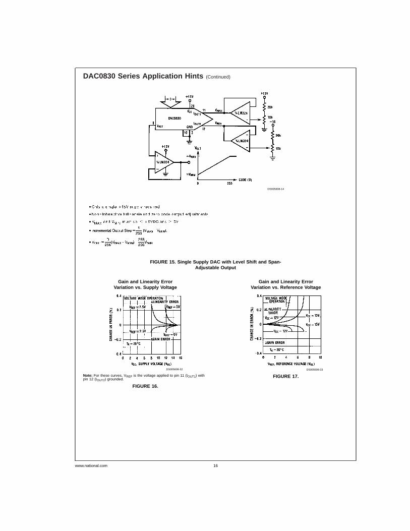
DAC0830 Series Application Hints (Continued)
DS005608-14
FIGURE 15. Single Supply DAC with Level Shift and Span-Adjustable Output
Gain and Linearity ErrorVariation vs. Supply Voltage
DS005608-32
Note: For these curves, VREF is the voltage applied to pin 11 (IOUT1) withpin 12 (IOUT2) grounded.
FIGURE 16.
Gain and Linearity ErrorVariation vs. Reference Voltage
DS005608-33
FIGURE 17.
www.national.com 16
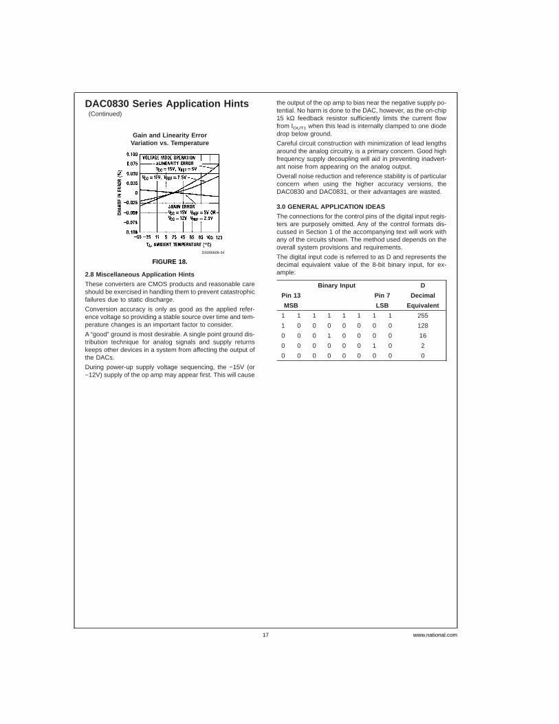
DAC0830 Series Application Hints(Continued)
2.8 Miscellaneous Application Hints
These converters are CMOS products and reasonable careshould be exercised in handling them to prevent catastrophicfailures due to static discharge.
Conversion accuracy is only as good as the applied refer-ence voltage so providing a stable source over time and tem-perature changes is an important factor to consider.
A “good” ground is most desirable. A single point ground dis-tribution technique for analog signals and supply returnskeeps other devices in a system from affecting the output ofthe DACs.
During power-up supply voltage sequencing, the −15V (or−12V) supply of the op amp may appear first. This will cause
the output of the op amp to bias near the negative supply po-tential. No harm is done to the DAC, however, as the on-chip15 kΩ feedback resistor sufficiently limits the current flowfrom IOUT1 when this lead is internally clamped to one diodedrop below ground.
Careful circuit construction with minimization of lead lengthsaround the analog circuitry, is a primary concern. Good highfrequency supply decoupling will aid in preventing inadvert-ant noise from appearing on the analog output.
Overall noise reduction and reference stability is of particularconcern when using the higher accuracy versions, theDAC0830 and DAC0831, or their advantages are wasted.
3.0 GENERAL APPLICATION IDEAS
The connections for the control pins of the digital input regis-ters are purposely omitted. Any of the control formats dis-cussed in Section 1 of the accompanying text will work withany of the circuits shown. The method used depends on theoverall system provisions and requirements.
The digital input code is referred to as D and represents thedecimal equivalent value of the 8-bit binary input, for ex-ample:
Binary Input D
Pin 13 Pin 7 Decimal
MSB LSB Equivalent
1 1 1 1 1 1 1 1 255
1 0 0 0 0 0 0 0 128
0 0 0 1 0 0 0 0 16
0 0 0 0 0 0 1 0 2
0 0 0 0 0 0 0 0 0
Gain and Linearity ErrorVariation vs. Temperature
DS005608-34
FIGURE 18.
www.national.com17

Applications
DAC Controlled Amplifier (Volume Control)
DS005608-43
Capacitance Multiplier
DS005608-44
Variable f O, Variable Q O, Constant BW Bandpass Filter
DS005608-17
www.national.com 18
Applications (Continued)
DAC Controlled Function Generator
DS005608-18
www.national.com19

Applications (Continued)
Two Terminal Floating 4 to 20 mA Current Loop Controller
DS005608-19
• DAC0830 linearly controls the current flow from the input terminal to the output terminal to be 4 mA (for D=0) to 19.94 mA (forD=255).
• Circuit operates with a terminal voltage differential of 16V to 55V.
• P2 adjusts the magnitude of the output current and P1 adjusts the zero to full scale range of output current.
• Digital inputs can be supplied from a processor using opto isolators on each input or the DAC latches can flow-through (con-nect control lines to pins 3 and 10 of the DAC) and the input data can be set by SPST toggle switches to ground (pins 3 and10).
www.national.com 20
Applications (Continued)
Ordering Information
Temperature Range 0˚C to +70˚ −40˚C to+85˚C
−55˚C to+125˚C
Non0.05%FSR
DAC0830LCN DAC0830LCM DAC0830LCV DAC0830LCJ DAC0830LJ
Linearity 0.1%FSR
DAC0831LCN
0.2%FSR
DAC0832LCN DAC0832LCM DAC0832LCV DAC0832LCJ DAC0832LJ
Package Outline N20A — MoldedDIP
M20B SmallOutline
V20A Chip Carrier J20A — Ceramic DIP
DAC Controlled Exponential Time Response
DS005608-20
• Output responds exponentially to input changes and automatically stops when VOUT=VIN
• Output time constant is directly proportional to the DAC input code and capacitor C
• Input voltage must be positive (See section 2.7)
www.national.com21

Physical Dimensions inches (millimeters) unless otherwise noted
Ceramic Dual-In-Line Package (J)Order Number DAC0830LCJ,
DAC0830LJ, DAC0832LJ or DAC0832LCJNS Package Number J20A
www.national.com 22
Physical Dimensions inches (millimeters) unless otherwise noted (Continued)
Molded Small Outline Package (M)Order Number DAC0830LCM
or DAC0832LCMNS Package Number M20B
Molded Dual-In-Line Package (N)Order Number DAC0830LCN,
or DAC0832LCNNS Package Number N20A
www.national.com23

Physical Dimensions inches (millimeters) unless otherwise noted (Continued)
LIFE SUPPORT POLICY
NATIONAL’S PRODUCTS ARE NOT AUTHORIZED FOR USE AS CRITICAL COMPONENTS IN LIFE SUPPORTDEVICES OR SYSTEMS WITHOUT THE EXPRESS WRITTEN APPROVAL OF THE PRESIDENT AND GENERALCOUNSEL OF NATIONAL SEMICONDUCTOR CORPORATION. As used herein:
1. Life support devices or systems are devices orsystems which, (a) are intended for surgical implantinto the body, or (b) support or sustain life, andwhose failure to perform when properly used inaccordance with instructions for use provided in thelabeling, can be reasonably expected to result in asignificant injury to the user.
2. A critical component is any component of a lifesupport device or system whose failure to performcan be reasonably expected to cause the failure ofthe life support device or system, or to affect itssafety or effectiveness.
National SemiconductorCorporationAmericasTel: 1-800-272-9959Fax: 1-800-737-7018Email: [email protected]
National SemiconductorEurope
Fax: +49 (0) 1 80-530 85 86Email: [email protected]
Deutsch Tel: +49 (0) 1 80-530 85 85English Tel: +49 (0) 1 80-532 78 32Français Tel: +49 (0) 1 80-532 93 58Italiano Tel: +49 (0) 1 80-534 16 80
National SemiconductorAsia Pacific CustomerResponse GroupTel: 65-2544466Fax: 65-2504466Email: [email protected]
National SemiconductorJapan Ltd.Tel: 81-3-5639-7560Fax: 81-3-5639-7507
www.national.com
Molded Chip Carrier (V)Order Number DAC0830LCV
or DAC0832LCVNS Package Number V20A
DA
C08
30/D
AC
0832
8-B
itµP
Com
patib
le,D
oubl
e-B
uffe
red
Dto
AC
onve
rters
National does not assume any responsibility for use of any circuitry described, no circuit patent licenses are implied and National reserves the right at any time without notice to change said circuitry and specifications.

©2001 Fairchild Semiconductor Corporation
www.fairchildsemi.com
Rev. 1.0.0
Features• Low input bias current• High input impedance• Wide gain bandwidth: 4 MHz Typ.• High slew rate: 13 V/µs Typ.
DescriptionThe LF347 is a high speed quad JFET input operationalamplifier. This feature high input impedance, widebandwidth, high slew rate, and low input offset voltage andbias current. LF347 may be used in circuits requiring highinput impedance. High slew rate and wide bandwidth, lowinput bias current.
14-DIP
1
14-SOP
1
Internal Block Diagram
LF347Quad Operational Amplifier (JFET)

LF347
2
Schematic Diagram(One Section Only)
Absolute Maximum RatingsParameter Symbol Value Unit
Supply Voltage VCC ±18 VDifferential Input Voltage VI(DIFF) 30 VInput Voltage Range VI ±15 VOutput Short Circuit Duration - Continuous -Power Dissipation PD 570 mWOperating Temperature Range TOPR 0 ~ + 70 °CStorage Temperature Range TSTG -65 ~ + 150 °C

LF347
3
Electrical Characteristics(VCC= +15V, VEE= -15V, TA=25 °C, unless otherwise specified)
Note :1. LF347 : 0≤TA≤+70 °C2. Guaranteed by design
Parameter Symbol ConditionsLF347
UnitMin. Typ. Max.
Input Offset Voltage VIORS = 10KΩ - 5 10
mVNote 1 - - 13
Input Offset Voltage Drift(Note2) ∆VIO/∆T RS = 10KΩ - 10 - µV/ °C
Input Offset Current IIO- 25 100 pA
Note 1 - - 4 nA
Input Bias Current IBIAS- 50 200 pA
Note 1 - - 8 nA
Large Signal Voltage Gain GVRL = 2KΩ 25 100 -
V/mVVO(P-P)= ±10V Note 1 15 - -
Output Voltage Swing VO(PP) RL = 10KΩ ±12 ±13.5 - V
Input Voltage Range VI(R) - ±11 +15-12 - V
Common-Mode Rejection Ratio CMRR RS ≤ 10KΩ 80 100 - dBPower Supply Rejection Ratio PSRR RS ≤ 10KΩ 80 100 - dBInput Resistance RI - - 1012 - ΩSupply Current ICC - - 7.2 11 mASlew Rate SR - - 13 - V/µSGain Bandwidth Product(Note2) GBW - - 4 - MHzChannel Seperation CS f = 1Hz ~ 20Khz
(input referenced) - 120 - dB
Equivalent Input NoiseVoltage eN
RS = 100Ωf = 1KHz - 20 - nV/
Equivalent Input NoiseCurrent IN f = 1KHz - 0.01 - pA/
Hz
Hz
LF347
4
Mechanical DimensionsPackage
Dimensions in millimeters
6.40 ±0.20
7.620.300
2.54
0.10
0
#1
#7 #8
#14
0.252 ±0.008
0~15°
0.25+0.10–0.05
0.010+0.004–0.002
3.30 ±0.30
0.130 ±0.012
3.25 ±0.20
0.128 ±0.008
19.4
0 ±0
.20
0.76
4 ±0
.008
19.8
00.
780
MA
X
5.080.200
0.200.008
MAX
MIN
2.08
0.08
2(
)
0.46
±0.
10
0.01
8 ±0
.004
0.05
9 ±0
.004
1.50
±0.
10
14-DIP

LF347
5
Mechanical Dimensions (Continued)
Package Dimensions in millimeters
8.56
±0.
20
0.33
7 ±0
.008
1.27
0.05
0
5.720.225
1.55 ±0.10
0.061 ±0.004
0.050.002
6.00 ±0.30
0.236 ±0.012
3.95 ±0.20
0.156 ±0.008
0.60 ±0.20
0.024 ±0.008
8.70
0.34
3M
AX
#1
#7 #8
0~8°
#14
0.47
0.01
9(
)
1.800.071
MA
X0.
10M
AX
0.00
4
MAX
MIN
+0.
10-0
.05
0.20
+0.
004
-0.0
020.
008
+0.
10-0
.05
0.40
6
+0.
004
-0.0
020.
016
14-SOP
LF347
6/1/01 0.0m 001Stock#DSxxxxxxxx
2001 Fairchild Semiconductor Corporation
LIFE SUPPORT POLICY FAIRCHILD’S PRODUCTS ARE NOT AUTHORIZED FOR USE AS CRITICAL COMPONENTS IN LIFE SUPPORT DEVICES OR SYSTEMS WITHOUT THE EXPRESS WRITTEN APPROVAL OF THE PRESIDENT OF FAIRCHILD SEMICONDUCTOR CORPORATION. As used herein:
1. Life support devices or systems are devices or systems which, (a) are intended for surgical implant into the body, or (b) support or sustain life, and (c) whose failure to perform when properly used in accordance with instructions for use provided in the labeling, can be reasonably expected to result in a significant injury of the user.
2. A critical component in any component of a life support device or system whose failure to perform can be reasonably expected to cause the failure of the life support device or system, or to affect its safety or effectiveness.
www.fairchildsemi.com
DISCLAIMER FAIRCHILD SEMICONDUCTOR RESERVES THE RIGHT TO MAKE CHANGES WITHOUT FURTHER NOTICE TO ANY PRODUCTS HEREIN TO IMPROVE RELIABILITY, FUNCTION OR DESIGN. FAIRCHILD DOES NOT ASSUME ANY LIABILITY ARISING OUT OF THE APPLICATION OR USE OF ANY PRODUCT OR CIRCUIT DESCRIBED HEREIN; NEITHER DOES IT CONVEY ANY LICENSE UNDER ITS PATENT RIGHTS, NOR THE RIGHTS OF OTHERS.
Ordering InformationProduct Number Package Operating Temperature
LF347N 14-DIP0 ~ + 70°C
LF347M 14-SOP

DATA SHEET
Product specificationSupersedes data of 1997 Jun 03File under Discrete Semiconductors, SC04
1997 Sep 03
DISCRETE SEMICONDUCTORS
BC107; BC108; BC109NPN general purpose transistors
M3D125

1997 Sep 03 2
Philips Semiconductors Product specification
NPN general purpose transistors BC107; BC108; BC109
FEATURES
• Low current (max. 100 mA)
• Low voltage (max. 45 V).
APPLICATIONS
• General purpose switching and amplification.
DESCRIPTION
NPN transistor in a TO-18; SOT18 metal package.PNP complement: BC177.
PINNING
PIN DESCRIPTION
1 emitter
2 base
3 collector, connected to the case
Fig.1 Simplified outline (TO-18; SOT18)and symbol.
handbook, halfpage
MAM2641
3
2
3
12
QUICK REFERENCE DATA
SYMBOL PARAMETER CONDITIONS MIN. MAX. UNIT
VCBO collector-base voltage open emitter
BC107 − 50 V
BC108; BC109 − 30 V
VCEO collector-emitter voltage open base
BC107 − 45 V
BC108; BC109 − 20 V
ICM peak collector current − 200 mA
Ptot total power dissipation Tamb ≤ 25 °C − 300 mW
hFE DC current gain IC = 2 mA; VCE = 5 V
BC107 110 450
BC108 110 800
BC109 200 800
fT transition frequency IC = 10 mA; VCE = 5 V; f = 100 MHz 100 − MHz

1997 Sep 03 3
Philips Semiconductors Product specification
NPN general purpose transistors BC107; BC108; BC109
LIMITING VALUESIn accordance with the Absolute Maximum Rating System (IEC 134).
THERMAL CHARACTERISTICS
Note
1. Transistor mounted on an FR4 printed-circuit board.
SYMBOL PARAMETER CONDITIONS MIN. MAX. UNIT
VCBO collector-base voltage open emitter
BC107 − 50 V
BC108; BC109 − 30 V
VCEO collector-emitter voltage open base
BC107 − 45 V
BC108; BC109 − 20 V
VEBO emitter-base voltage open collector
BC107 − 6 V
BC108; BC109 − 5 V
IC collector current (DC) − 100 mA
ICM peak collector current − 200 mA
IBM peak base current − 200 mA
Ptot total power dissipation Tamb ≤ 25 °C − 300 mW
Tstg storage temperature −65 +150 °CTj junction temperature − 175 °CTamb operating ambient temperature −65 +150 °C
SYMBOL PARAMETER CONDITIONS VALUE UNIT
Rth j-a thermal resistance from junction to ambient note 1 0.5 K/mW
Rth j-c thermal resistance from junction to case 0.2 K/mW
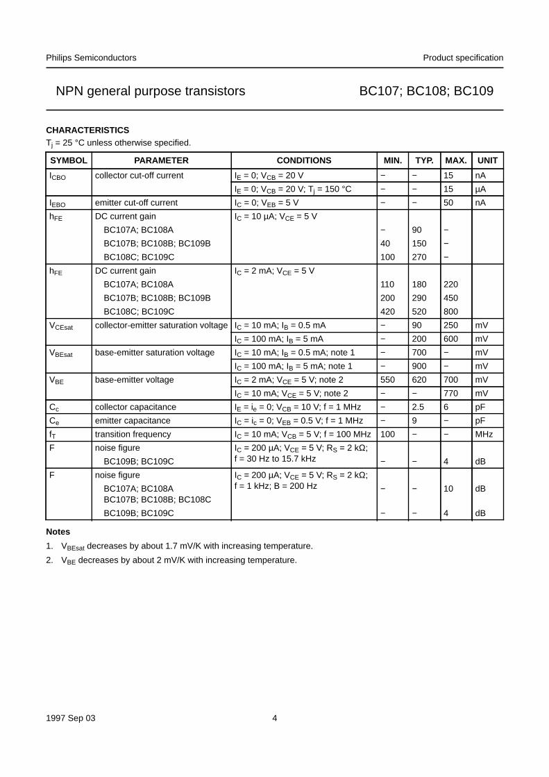
1997 Sep 03 4
Philips Semiconductors Product specification
NPN general purpose transistors BC107; BC108; BC109
CHARACTERISTICSTj = 25 °C unless otherwise specified.
Notes
1. VBEsat decreases by about 1.7 mV/K with increasing temperature.
2. VBE decreases by about 2 mV/K with increasing temperature.
SYMBOL PARAMETER CONDITIONS MIN. TYP. MAX. UNIT
ICBO collector cut-off current IE = 0; VCB = 20 V − − 15 nA
IE = 0; VCB = 20 V; Tj = 150 °C − − 15 µA
IEBO emitter cut-off current IC = 0; VEB = 5 V − − 50 nA
hFE DC current gain IC = 10 µA; VCE = 5 V
BC107A; BC108A − 90 −BC107B; BC108B; BC109B 40 150 −BC108C; BC109C 100 270 −
hFE DC current gain IC = 2 mA; VCE = 5 V
BC107A; BC108A 110 180 220
BC107B; BC108B; BC109B 200 290 450
BC108C; BC109C 420 520 800
VCEsat collector-emitter saturation voltage IC = 10 mA; IB = 0.5 mA − 90 250 mV
IC = 100 mA; IB = 5 mA − 200 600 mV
VBEsat base-emitter saturation voltage IC = 10 mA; IB = 0.5 mA; note 1 − 700 − mV
IC = 100 mA; IB = 5 mA; note 1 − 900 − mV
VBE base-emitter voltage IC = 2 mA; VCE = 5 V; note 2 550 620 700 mV
IC = 10 mA; VCE = 5 V; note 2 − − 770 mV
Cc collector capacitance IE = ie = 0; VCB = 10 V; f = 1 MHz − 2.5 6 pF
Ce emitter capacitance IC = ic = 0; VEB = 0.5 V; f = 1 MHz − 9 − pF
fT transition frequency IC = 10 mA; VCB = 5 V; f = 100 MHz 100 − − MHz
F noise figure IC = 200 µA; VCE = 5 V; RS = 2 kΩ;f = 30 Hz to 15.7 kHzBC109B; BC109C − − 4 dB
F noise figure IC = 200 µA; VCE = 5 V; RS = 2 kΩ;f = 1 kHz; B = 200 HzBC107A; BC108A
BC107B; BC108B; BC108C− − 10 dB
BC109B; BC109C − − 4 dB

1997 Sep 03 5
Philips Semiconductors Product specification
NPN general purpose transistors BC107; BC108; BC109
PACKAGE OUTLINE
REFERENCESOUTLINEVERSION
EUROPEANPROJECTION ISSUE DATE
IEC JEDEC EIAJ
SOT18/13 TO-18B11/C7 type 3 97-04-18
a
α
k
D A L
seating plane
b
D1
0 5 10 mm
scale
Metal-can cylindrical single-ended package; 3 leads SOT18/13
w AM M B M
A
1
2
3
j
B
DIMENSIONS (millimetre dimensions are derived from the original inch dimensions)
UNIT w
mm 5.314.74
0.470.41
5.455.30
4.704.55
1.030.94
1.10.9
15.012.7
α
0.40 45°
A a b D D1 j k L
2.54

1997 Sep 03 6
Philips Semiconductors Product specification
NPN general purpose transistors BC107; BC108; BC109
DEFINITIONS
LIFE SUPPORT APPLICATIONS
These products are not designed for use in life support appliances, devices, or systems where malfunction of theseproducts can reasonably be expected to result in personal injury. Philips customers using or selling these products foruse in such applications do so at their own risk and agree to fully indemnify Philips for any damages resulting from suchimproper use or sale.
Data Sheet Status
Objective specification This data sheet contains target or goal specifications for product development.
Preliminary specification This data sheet contains preliminary data; supplementary data may be published later.
Product specification This data sheet contains final product specifications.
Limiting values
Limiting values given are in accordance with the Absolute Maximum Rating System (IEC 134). Stress above one ormore of the limiting values may cause permanent damage to the device. These are stress ratings only and operationof the device at these or at any other conditions above those given in the Characteristics sections of the specificationis not implied. Exposure to limiting values for extended periods may affect device reliability.
Application information
Where application information is given, it is advisory and does not form part of the specification.

1997 Sep 03 7
Philips Semiconductors Product specification
NPN general purpose transistors BC107; BC108; BC109
NOTES

Internet: http://www.semiconductors.philips.com
Philips Semiconductors – a worldwide company
© Philips Electronics N.V. 1997 SCA55
All rights are reserved. Reproduction in whole or in part is prohibited without the prior written consent of the copyright owner.
The information presented in this document does not form part of any quotation or contract, is believed to be accurate and reliable and may be changedwithout notice. No liability will be accepted by the publisher for any consequence of its use. Publication thereof does not convey nor imply any licenseunder patent- or other industrial or intellectual property rights.
Netherlands: Postbus 90050, 5600 PB EINDHOVEN, Bldg. VB,Tel. +31 40 27 82785, Fax. +31 40 27 88399
New Zealand: 2 Wagener Place, C.P.O. Box 1041, AUCKLAND,Tel. +64 9 849 4160, Fax. +64 9 849 7811
Norway: Box 1, Manglerud 0612, OSLO,Tel. +47 22 74 8000, Fax. +47 22 74 8341
Philippines: Philips Semiconductors Philippines Inc.,106 Valero St. Salcedo Village, P.O. Box 2108 MCC, MAKATI,Metro MANILA, Tel. +63 2 816 6380, Fax. +63 2 817 3474
Poland: Ul. Lukiska 10, PL 04-123 WARSZAWA,Tel. +48 22 612 2831, Fax. +48 22 612 2327
Portugal: see Spain
Romania: see Italy
Russia: Philips Russia, Ul. Usatcheva 35A, 119048 MOSCOW,Tel. +7 095 755 6918, Fax. +7 095 755 6919
Singapore: Lorong 1, Toa Payoh, SINGAPORE 1231,Tel. +65 350 2538, Fax. +65 251 6500
Slovakia: see Austria
Slovenia: see Italy
South Africa: S.A. PHILIPS Pty Ltd., 195-215 Main Road Martindale,2092 JOHANNESBURG, P.O. Box 7430 Johannesburg 2000,Tel. +27 11 470 5911, Fax. +27 11 470 5494
South America: Rua do Rocio 220, 5th floor, Suite 51,04552-903 São Paulo, SÃO PAULO - SP, Brazil,Tel. +55 11 821 2333, Fax. +55 11 829 1849
Spain: Balmes 22, 08007 BARCELONA,Tel. +34 3 301 6312, Fax. +34 3 301 4107
Sweden: Kottbygatan 7, Akalla, S-16485 STOCKHOLM,Tel. +46 8 632 2000, Fax. +46 8 632 2745
Switzerland: Allmendstrasse 140, CH-8027 ZÜRICH,Tel. +41 1 488 2686, Fax. +41 1 481 7730
Taiwan: Philips Semiconductors, 6F, No. 96, Chien Kuo N. Rd., Sec. 1,TAIPEI, Taiwan Tel. +886 2 2134 2865, Fax. +886 2 2134 2874
Thailand: PHILIPS ELECTRONICS (THAILAND) Ltd.,209/2 Sanpavuth-Bangna Road Prakanong, BANGKOK 10260,Tel. +66 2 745 4090, Fax. +66 2 398 0793
Turkey: Talatpasa Cad. No. 5, 80640 GÜLTEPE/ISTANBUL,Tel. +90 212 279 2770, Fax. +90 212 282 6707
Ukraine : PHILIPS UKRAINE, 4 Patrice Lumumba str., Building B, Floor 7,252042 KIEV, Tel. +380 44 264 2776, Fax. +380 44 268 0461
United Kingdom: Philips Semiconductors Ltd., 276 Bath Road, Hayes,MIDDLESEX UB3 5BX, Tel. +44 181 730 5000, Fax. +44 181 754 8421
United States: 811 East Arques Avenue, SUNNYVALE, CA 94088-3409,Tel. +1 800 234 7381
Uruguay: see South America
Vietnam: see Singapore
Yugoslavia: PHILIPS, Trg N. Pasica 5/v, 11000 BEOGRAD,Tel. +381 11 625 344, Fax.+381 11 635 777
For all other countries apply to: Philips Semiconductors, Marketing & Sales Communications,Building BE-p, P.O. Box 218, 5600 MD EINDHOVEN, The Netherlands, Fax. +31 40 27 24825
Argentina: see South America
Australia: 34 Waterloo Road, NORTH RYDE, NSW 2113,Tel. +61 2 9805 4455, Fax. +61 2 9805 4466
Austria: Computerstr. 6, A-1101 WIEN, P.O. Box 213, Tel. +43 160 1010,Fax. +43 160 101 1210
Belarus: Hotel Minsk Business Center, Bld. 3, r. 1211, Volodarski Str. 6,220050 MINSK, Tel. +375 172 200 733, Fax. +375 172 200 773
Belgium: see The Netherlands
Brazil: see South America
Bulgaria: Philips Bulgaria Ltd., Energoproject, 15th floor,51 James Bourchier Blvd., 1407 SOFIA,Tel. +359 2 689 211, Fax. +359 2 689 102
Canada: PHILIPS SEMICONDUCTORS/COMPONENTS,Tel. +1 800 234 7381
China/Hong Kong: 501 Hong Kong Industrial Technology Centre,72 Tat Chee Avenue, Kowloon Tong, HONG KONG,Tel. +852 2319 7888, Fax. +852 2319 7700
Colombia: see South America
Czech Republic: see Austria
Denmark: Prags Boulevard 80, PB 1919, DK-2300 COPENHAGEN S,Tel. +45 32 88 2636, Fax. +45 31 57 0044
Finland: Sinikalliontie 3, FIN-02630 ESPOO,Tel. +358 9 615800, Fax. +358 9 61580920
France: 4 Rue du Port-aux-Vins, BP317, 92156 SURESNES Cedex,Tel. +33 1 40 99 6161, Fax. +33 1 40 99 6427
Germany: Hammerbrookstraße 69, D-20097 HAMBURG,Tel. +49 40 23 53 60, Fax. +49 40 23 536 300
Greece: No. 15, 25th March Street, GR 17778 TAVROS/ATHENS,Tel. +30 1 4894 339/239, Fax. +30 1 4814 240
Hungary: see Austria
India: Philips INDIA Ltd, Band Box Building, 2nd floor,254-D, Dr. Annie Besant Road, Worli, MUMBAI 400 025,Tel. +91 22 493 8541, Fax. +91 22 493 0966
Indonesia: see Singapore
Ireland: Newstead, Clonskeagh, DUBLIN 14,Tel. +353 1 7640 000, Fax. +353 1 7640 200
Israel: RAPAC Electronics, 7 Kehilat Saloniki St, PO Box 18053,TEL AVIV 61180, Tel. +972 3 645 0444, Fax. +972 3 649 1007
Italy: PHILIPS SEMICONDUCTORS, Piazza IV Novembre 3,20124 MILANO, Tel. +39 2 6752 2531, Fax. +39 2 6752 2557
Japan: Philips Bldg 13-37, Kohnan 2-chome, Minato-ku, TOKYO 108,Tel. +81 3 3740 5130, Fax. +81 3 3740 5077
Korea: Philips House, 260-199 Itaewon-dong, Yongsan-ku, SEOUL,Tel. +82 2 709 1412, Fax. +82 2 709 1415
Malaysia: No. 76 Jalan Universiti, 46200 PETALING JAYA, SELANGOR,Tel. +60 3 750 5214, Fax. +60 3 757 4880
Mexico: 5900 Gateway East, Suite 200, EL PASO, TEXAS 79905,Tel. +9-5 800 234 7381
Middle East: see Italy
Printed in The Netherlands 117047/00/04/pp8 Date of release: 1997 Sep 03 Document order number: 9397 750 02817

This datasheet has been download from:
www.datasheetcatalog.com
Datasheets for electronics components.
Related Documents


![[UU] Rangkaian Digital](https://static.cupdf.com/doc/110x72/55cf8e9e550346703b940471/uu-rangkaian-digital.jpg)
