OPTICS EXPRESS Vol. 24, No. 15 | 25 Jul 2016 | 16574 Feasibility study on 3-D shape analysis of high- aspect-ratio features using through-focus scanning optical microscopy Ravi Kiran Attota, 1* Peter Weck, 2 John A. Kramar, 1 Benjamin Bunday 3 and Victor Vartanian 3 1 Engineering Physics Division, PML, NIST, Gaithersburg, MD 20899, USA 2 Swarthmore College, 500 College Ave., Swarthmore, PA 19081, USA 3 SUNY Politechnic SEMATECH, 257 Fuller Road, Suite 2200, Albany, NY, 12203, USA * [email protected] Abstract: In-line metrologies currently used in the semiconductor industry are being challenged by the aggressive pace of device scaling and the adoption of novel device architectures. Metrology and process control of three-dimensional (3-D) high-aspect-ratio (HAR) features are becoming increasingly important and also challenging. In this paper we present a feasibility study of through-focus scanning optical microscopy (TSOM) for 3-D shape analysis of HAR features. TSOM makes use of 3-D optical data collected using a conventional optical microscope for 3-D shape analysis. Simulation results of trenches and holes down to the 11 nm node are presented. The ability of TSOM to analyze an array of HAR features or a single isolated HAR feature is also presented. This allows for the use of targets with area over 100 times smaller than that of conventional gratings, saving valuable real estate on the wafers. Indications are that the sensitivity of TSOM may match or exceed the International Technology Roadmap for Semiconductors (ITRS) measurement requirements for the next several years. Both simulations and preliminary experimental results are presented. The simplicity, lowcost, high throughput, and nanometer scale 3-D shape sensitivity of TSOM make it an attractive inspection and process monitoring solution for nanomanufacturing. 2016 Optical Society of America OCIS codes: (120.0120) Instrumentation, measurement, and metrology; (120.3930) Metrological instrumentation; (180.5810) Scanning microscopy; (180.6900) Three-dimensional microscopy. References and links 1. J. Vila-Comamala, S. Gorelick, V. A. Guzenko, E. Farm, M. Ritala, and C. David, "Dense high aspect ratio hydrogen silsesquioxane nanostructures by 100 keV electron beam lithography," Nanotechnology 21, 285305 (2010). 2. C. Chang and A. Sakdinawat, "Ultra-high aspect ratio high-resolution nanofabrication for hard X-ray diffractive optics," Nat. Commun. 5, 4243 (2014). 3. B. Bunday, T. A. Germer, V. Vartanian, A. Cordes, A. Cepler, and C. Settens, "Gaps analysis for CD metrology beyond the 22 nm node," Proc. SPIE 8681, 86813B (2013). 4. T. M. Bao, Y. Bar, D. Fong, and M. Godbole, "Improving dry etch control for contact plugs in advanced DRAM manufacturing," Proc. SPIE 6922, 69223G (2008). 5. A. W. Topol, D. C. L. Tulipe, L. Shi, D. J. Frank, K. Bernstein, S. E. Steen, A. Kumar, G. U. Singco, A. M. Young, K. W. Guarini, and M. Ieong, "Three-dimensional integrated circuits," IBM Journal of Research and Development 50, 491-506 (2006). 6. Y. S. Ku, D. M. Shyu, P. Y. Chang, and W. T. Hsu, "In-line metrology of 3D interconnect processes," Proc. SPIE 8324, 832411 (2012). 7. O. Fursenko, J. Bauer, S. Marschmeyer, and H. P. Stoll, "Through silicon via profile metrology of Bosch etching process based on spectroscopic reflectometry," Microelectron Eng. 139, 70-75 (2015).

Welcome message from author
This document is posted to help you gain knowledge. Please leave a comment to let me know what you think about it! Share it to your friends and learn new things together.
Transcript
OPTICS EXPRESS Vol. 24, No. 15 | 25 Jul 2016 | 16574
Feasibility study on 3-D shape analysis of high-
aspect-ratio features using through-focus
scanning optical microscopy
Ravi Kiran Attota,1* Peter Weck,2 John A. Kramar,1 Benjamin Bunday3
and Victor Vartanian3
1Engineering Physics Division, PML, NIST, Gaithersburg, MD 20899, USA 2Swarthmore College, 500 College Ave., Swarthmore, PA 19081, USA
3SUNY Politechnic SEMATECH, 257 Fuller Road, Suite 2200, Albany, NY, 12203, USA *[email protected]
Abstract: In-line metrologies currently used in the semiconductor industry
are being challenged by the aggressive pace of device scaling and the
adoption of novel device architectures. Metrology and process control of
three-dimensional (3-D) high-aspect-ratio (HAR) features are becoming
increasingly important and also challenging. In this paper we present a
feasibility study of through-focus scanning optical microscopy (TSOM) for
3-D shape analysis of HAR features. TSOM makes use of 3-D optical data
collected using a conventional optical microscope for 3-D shape analysis.
Simulation results of trenches and holes down to the 11 nm node are
presented. The ability of TSOM to analyze an array of HAR features or a
single isolated HAR feature is also presented. This allows for the use of
targets with area over 100 times smaller than that of conventional gratings,
saving valuable real estate on the wafers. Indications are that the sensitivity
of TSOM may match or exceed the International Technology Roadmap for
Semiconductors (ITRS) measurement requirements for the next several
years. Both simulations and preliminary experimental results are presented.
The simplicity, lowcost, high throughput, and nanometer scale 3-D shape
sensitivity of TSOM make it an attractive inspection and process monitoring
solution for nanomanufacturing.
2016 Optical Society of America
OCIS codes: (120.0120) Instrumentation, measurement, and metrology; (120.3930)
Metrological instrumentation; (180.5810) Scanning microscopy; (180.6900) Three-dimensional
microscopy.
References and links
1. J. Vila-Comamala, S. Gorelick, V. A. Guzenko, E. Farm, M. Ritala, and C. David, "Dense high aspect ratio hydrogen silsesquioxane nanostructures by 100 keV electron beam lithography," Nanotechnology 21, 285305
(2010).
2. C. Chang and A. Sakdinawat, "Ultra-high aspect ratio high-resolution nanofabrication for hard X-ray diffractive optics," Nat. Commun. 5, 4243 (2014).
3. B. Bunday, T. A. Germer, V. Vartanian, A. Cordes, A. Cepler, and C. Settens, "Gaps analysis for CD metrology
beyond the 22 nm node," Proc. SPIE 8681, 86813B (2013).
4. T. M. Bao, Y. Bar, D. Fong, and M. Godbole, "Improving dry etch control for contact plugs in advanced DRAM
manufacturing," Proc. SPIE 6922, 69223G (2008).
5. A. W. Topol, D. C. L. Tulipe, L. Shi, D. J. Frank, K. Bernstein, S. E. Steen, A. Kumar, G. U. Singco, A. M. Young, K. W. Guarini, and M. Ieong, "Three-dimensional integrated circuits," IBM Journal of Research and
Development 50, 491-506 (2006).
6. Y. S. Ku, D. M. Shyu, P. Y. Chang, and W. T. Hsu, "In-line metrology of 3D interconnect processes," Proc. SPIE 8324, 832411 (2012).
7. O. Fursenko, J. Bauer, S. Marschmeyer, and H. P. Stoll, "Through silicon via profile metrology of Bosch etching
process based on spectroscopic reflectometry," Microelectron Eng. 139, 70-75 (2015).
OPTICS EXPRESS Vol. 24, No. 15 | 25 Jul 2016 | 16574
8. M. Nakamura, H. Kitada, and S. Sakuyama, "Direct depth measurement tool of high aspect ratio via-hole for
three-dimensional stacked devices," J. Surface Analysis 20, 182-186 (2014). 9. K. Takamasu, Y. Iwaki, S. Takahashi, H. Kawada, M. Ikota, G. F. Lorusso, and N. Horiguchi, "3D-profile
measurement of advanced semiconductor features by reference metrology," Proc. SPIE 9778, 97781T (2016).
10. I. Schulmeyer, L. Lechner, A. Gu, R. Estrada, D. Stewart, L. Stern, S. McVey, B. Goetze, U. Mantz, and R. Jammy, "Advanced metrology and inspection solutions for a 3D world," Proc. 2016 International Symposium
on VLSI Technology, Systems and Application (VLSI-TSA), 1-2 (2016).
11. A. J. Cepler, B. Bunday, B. L. Thiel, and J. S. Villarrubia, "Scanning electron microscopy imaging of ultra-high aspect ratio hole features," Proc. SPIE 8324, 83241N (2012).
12. A. Arceo, B. Bunday, A. Cordes, and V. Vartanian, "Evolution or revolution: the path for metrology beyond the
22nm node," Solid State Technol 55, 15-19 (2012). 13. R. K. Leach, R. Boyd, T. Burke, H. U. Danzebrink, K. Dirscherl, T. Dziomba, M. Gee, L. Koenders, V.
Morazzani, A. Pidduck, D. Roy, W. E. S. Unger, and A. Yacoot, "The European nanometrology landscape,"
Nanotechnology 22, 062001 (2011). 14. R. A. Allen, V. Vartanian, D. Read, and W. Baylies, "(Invited) Metrology for 3D Integration," Ecs Transactions
61, 105-112 (2014).
15. T. M. Bao, L. Mininni, and D. Dawson, "Improving sidewall profile metrology with enhanced 3D-AFM," Lithography Asia 2008, 7140 (2008).
16. M. Caldwell, T. M. Bao, J. Hackenberg, B. McLain, O. Munoz, T. Stephens, and V. Vartanian, "Improved
dimension and shape metrology with versatile atomic force microscopy,” Proc. SPIE 6518, 65181L (2007). 17. W. Hassler-Grohne, D. Huser, K. P. Johnsen, C. G. Frase, and H. Bosse, "Current limitations of SEM and AFM
metrology for the characterization of 3D nanostructures," Meas. Sci. Technol 22, 094003 (2011).
18. Y. S. Ku, "Spectral reflectometry for metrology of three-dimensional through-silicon vias," J Micro-Nanolith Mem. 13, 011209 (2014).
19. X. X. Zhang, P. Snow, A. Vaid, E. Solecky, H. Zhou, Z. H. Ge, S. Yasharzade, O. Shoval, O. Adan, I.
Schwarzband, and M. Bar-Zvi, "Solving next generation (1X node) metrology challenges using advanced CDSEM capabilities: tilt, high energy and backscatter imaging," Proc. SPIE 9424, 94240G (2015).
20. V. Vartanian, R. A. Allen, L. Smith, K. Hummler, S. Olson, and B. Sapp, "Metrology needs for through-silicon via fabrication," MOEMS 13, 011206-011206 (2014).
21. S. I. Association, "The International Technology Roadmap for Semiconductors (ITRS) " (Semiconductor
Industry Association, San Jose, 2011). 22. B. Bunday, "HVM metrology challenges towards the 5nm node," Proc. SPIE 9778, 97780E (2016).
23. R. Attota, T. A. Germer, and R. M. Silver, "Through-focus scanning-optical-microscope imaging method for
nanoscale dimensional analysis," Opt. Lett. 33, 1990-1992 (2008). 24. R. Attota, R. G. Dixson, J. A. Kramar, J. E. Potzick, A. E. Vladar, B. Bunday, E. Novak, and A. Rudack, "TSOM
method for semiconductor metrology," Proc. SPIE 7971, 79710T (2011).
25. R. Attota and R. G. Dixson, "Resolving three-dimensional shape of sub-50 nm wide lines with nanometer-scale
sensitivity using conventional optical microscopes," Appl. Phys. Lett. 105, 043101 (2014).
26. M. Ryabko, Koptyev, S., Shchekin, A., Medvedev, A., "Improved critical dimension inspection for the
semiconductor industry," SPIE Newsroom (2014). 27. M. Ryabko, S. Koptyaev, A. Shcherbakov, A. Lantsov, and S. Y. Oh, “Motion-free all optical inspection system
for nanoscale topology control,” Opt. Express 22, 14958–14963 (2014).
28. M. Ryabko, A. Shchekin, S. Koptyaev, A. Lantsov, A. Medvedev, A. Shcherbakov, and S. Y. Oh, “Throughfocus scanning optical microscopy (TSOM) considering optical aberrations: practical implementation,” Opt. Exp. 23,
32215–32221 (2015).
29. R. Attota and R. Silver, "Nanometrology using a through-focus scanning optical microscopy method," Meas. Sci. Technol. 22, 024002 (2011).
30. H. Kang, R. Attota, V. Tondare, A. E. Vladár, and P. Kavuri, "A method to determine the number of nanoparticles
in a cluster using conventional optical microscopes," Appl. Phys. Lett. 107, 103106 (2015). 31. R. Attota, "Noise analysis for through-focus scanning optical microscopy," Opt. Lett. 41, 745-748 (2016).
32. T. Pistor, V., "Electromagnetic simulation and modeling with applications in lithography," (University of
California, Berkeley, 2001). 33. C. Hartig, D. Fischer, B. Schulz, A. Vaid, O. Adan, S. Levi, A. Ge, J. Zhou, M. Bar-Zvi, R. Enge, and U. Groh,
"Material contrast based inline metrology - process verification and control using Back Scattered Electron
Imaging on CD-SEM," Proc. SPIE 8681, 868108 (2013).
34. A. J. Cepler, B. Bunday, B. L. Thiel, and J. S. Villarrubia, "Scanning electron microscopy imaging of ultra-high
aspect ratio hole features," Proc. SPIE 8324, 83241N (2012).
35. R. K. Attota and H. Kang, "Parameter optimization for through-focus scanning optical microscopy," Opt. Exp. 24, 14915-14924 (2016).
36. R. Attota, P. P. Kavuri, H. Kang, R. Kasica, and L. Chen, "Nanoparticle size determination using optical
microscopes," Appl. Phys. Lett. 105, 163105 (2014). 37. J. M. Gineste, P. Macko, E. A. Patterson, and M. P. Whelan, "Three-dimensional automated nanoparticle tracking
using Mie scattering in an optical microscope," J. of Microscopy 243, 172-178 (2011).

OPTICS EXPRESS Vol. 24, No. 15 | 25 Jul 2016 | 16574
1. Introduction
Dimensional metrology of high aspect ratio (HAR) features [1-11] will become more
challenging as technology progresses, particularly in memory applications where designs are
evolving from planar to vertical architectures with multi-level gates assembled in 3-D structures
[3, 11-20]. The basic building blocks of these features are deep trenches and holes in oxide,
silicon, or multiple alternating layers of oxide and silicon. Furthermore, memory device scaling
is headed towards aspect ratios ranging from 30:1 to 60:1, implying depths from 0.5 μm to 2
μm at the 32 nm and 11 nm International Technology Roadmap for Semiconductors (ITRS)
node [3, 21] lateral dimensions. For example, HAR contact holes may be 1 m in depth and 30
nm in diameter, for an aspect ratio of approximately 30:1 at the 32 nm node. From the process
control perspective, CD metrology entails control of top CD, bottom CD, profile, and detection
of residues, which introduce a new set of gaps in metrology capability, since current non-
destructive metrology techniques lack the sensitivity and resolution to characterize such
features [22]. Moreover, the physics of these measurements are hindered by the extremely deep
and geometrically confined volumes involved. Charged particle-based imaging techniques
such as CD scanning electron microscopy (CD-SEM), and helium ion microscopy (HeIM) have
sensitivity limitations arising from sidewall charging, as only a small fraction of scattered
particles ultimately reaches the detector.
The limitations outlined above prompt the need for alternative non-destructive metrology
methods that can achieve sensitivity at the nanoscale while maintaining throughput compatible
with high volume manufacturing. In light of this, optical techniques are desirable. A recently
developed optical method is through-focus scanning optical microscopy (TSOM). In this paper
we explore the application of TSOM for 3-D shape analysis of HAR targets, especially as an
inspection and process monitoring tool. TSOM is a measurement technique that has the
potential to fulfill the requirements of a non-destructive, high-throughput method with
sensitivity on the nanometer scale [23-30]. The low cost of TSOM makes it a potential
candidate for measuring features in high-volume manufacturing. In this work, we performed a
series of simulations to examine the usage of TSOM for HAR CD metrology, and demonstrate
this method using a test HAR trench wafer.
2.TSOM
TSOM makes use of a conventional optical microscope equipped with a digital camera and a
motorized focus stage, and consists of collecting optical images at a range of focus positions
and combining them into a 3-D volume of optical information. Preserving all available optical
information in this 3-D space (x, y, and focus position) allows for performing dimensional
analysis of a sample by generating a 2-D TSOM image from any direction or location in the
x-y plane as a function of focus position [23, 25, 29]. A differential TSOM (D-TSOM) image
is a pixel-by-pixel difference between two TSOM images. Three of the several important
properties of D-TSOM images [24, 29] are given below.
1. D-TSOM images are often distinct for different types of parameter changes
2. D-TSOM images are qualitatively similar for different magnitude changes in the same
parameter
3. Optical content of a D-TSOM image is proportional to the magnitude of the
dimensional differences
Property 1 means that the D-TSOM images can serve as a “fingerprint” for different types
of parameter variations. Property 2 means variation in a given parameter will scale the
magnitude of the D-TSOM image without significantly changing its shape. Property 3 provides
the magnitude of the difference and can be quantified with an optical intensity range (OIR)
OPTICS EXPRESS Vol. 24, No. 15 | 25 Jul 2016 | 16574
metric [25], which is the absolute optical range of the differential signal and is scaled by 100.
In the current work, we make use of these three D-TSOM image characteristics to determine
3-D shape variations of HAR structures.
This work contains both experiments and simulations. It is important to understand the
experimental noise threshold to understand the sensitivity limitations of the simulation results
and to determine whether a simulated TSOM result from a feature dimension perturbation
would be distinguishable from background noise. It was found that the noise OIR of less than
one provides an experimental noise threshold limit for the subsequent simulations [31]. To
experimentally detect a dimensional difference safely, it is desirable to have the OIR of a
D-TSOM image greater than one.
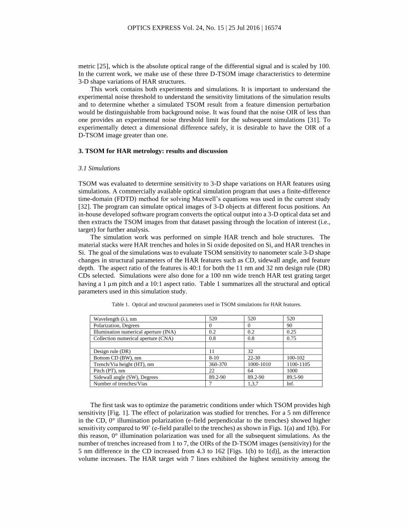
3. TSOM for HAR metrology: results and discussion
3.1 Simulations
TSOM was evaluated to determine sensitivity to 3-D shape variations on HAR features using
simulations. A commercially available optical simulation program that uses a finite-difference
time-domain (FDTD) method for solving Maxwell’s equations was used in the current study
[32]. The program can simulate optical images of 3-D objects at different focus positions. An
in-house developed software program converts the optical output into a 3-D optical data set and
then extracts the TSOM images from that dataset passing through the location of interest (i.e.,
target) for further analysis.
The simulation work was performed on simple HAR trench and hole structures. The
material stacks were HAR trenches and holes in Si oxide deposited on Si, and HAR trenches in
Si. The goal of the simulations was to evaluate TSOM sensitivity to nanometer scale 3-D shape
changes in structural parameters of the HAR features such as CD, sidewall angle, and feature
depth. The aspect ratio of the features is 40:1 for both the 11 nm and 32 nm design rule (DR)
CDs selected. Simulations were also done for a 100 nm wide trench HAR test grating target
having a 1 m pitch and a 10:1 aspect ratio. Table 1 summarizes all the structural and optical
parameters used in this simulation study.
The first task was to optimize the parametric conditions under which TSOM provides high
sensitivity [Fig. 1]. The effect of polarization was studied for trenches. For a 5 nm difference
in the CD, 0° illumination polarization (e-field perpendicular to the trenches) showed higher
sensitivity compared to 90˚ (e-field parallel to the trenches) as shown in Figs. 1(a) and 1(b). For
this reason, 0° illumination polarization was used for all the subsequent simulations. As the
number of trenches increased from 1 to 7, the OIRs of the D-TSOM images (sensitivity) for the
5 nm difference in the CD increased from 4.3 to 162 [Figs. 1(b) to 1(d)], as the interaction
volume increases. The HAR target with 7 lines exhibited the highest sensitivity among the
Table 1. Optical and structural parameters used in TSOM simulations for HAR features.
Wavelength (, nm 520 520 520
Polarization, Degrees 0 0 90
Illumination numerical aperture (INA) 0.2 0.2 0.25
Collection numerical aperture (CNA) 0.8 0.8 0.75
Design rule (DR) 11 32
Bottom CD (BW), nm 8-10 22-30 100-102
Trench/Via height (HT), nm 360-370 1000-1010 1100-1105
Pitch (PT), nm 22 64 1000
Sidewall angle (SW), Degrees 89.2-90 89.2-90 89.5-90
Number of trenches/Vias 7 1,3,7 Inf.

OPTICS EXPRESS Vol. 24, No. 15 | 25 Jul 2016 | 16574
targets studied. Consequently, a 7-trench HAR target was used for subsequent trench target
studies. For the hole simulations, an array of 9 holes across was used, with periodic boundary
conditions (i.e., infinite array of holes) at the hole spacing in the other dimension.
Fig.1. Selection of the optimized illumination polarization and the number of trenches, using HAR trenches in Si target as an example. Illumination polarization of 0o and increasing the number of trenches produce high sensitivity.
Polarization state and OIR values are shown in the insets.
Trench/hole depth, sidewall angle, and bottom CD are some of the important parameters
to monitor during fabrication. Therefore, variations in these parameters were studied for the
parameter ranges shown in Table 1. Following industry requirements, trenches in Si and
trenches and holes in oxide were studied [3]. The results for the 11 nm and 32 nm DR trench
and hole structures are shown in Figs. 2 and 3. To arrive at the sensitivity threshold, each
parameter was individually perturbed in small increments. D-TSOM images were evaluated at
each new condition with reduced differences in parameters until the OIR was just above one.
Under the simulation conditions used, the overall TSOM sensitivity is similar for a 0.01˚
sidewall angle perturbation for all HAR targets studied for the two selected DRs. The CD
parameter shows the best sensitivity: down to a 0.02 nm perturbation for 32 nm DR trenches.
The worst CD sensitivity is 0.1 nm for 11 nm DR trenches in oxide. Depth sensitivity shows
large variation among the two DRs studied, the smallest being 0.2 nm for 32 nm DR holes and
the largest being 5 nm for 11 nm DR holes. This indicates strong dependence of depth
sensitivity based on DR. A summary of potential TSOM sensitivities along with their
percentage sensitivities is shown in Table. 2.
For trenches in Si, each depth, sidewall angle, and bottom CD variation resulted in
dissimilar D-TSOM image patterns indicating that, in principle, these three parameters can be
distinguished. However, for HAR trenches and holes in oxide, CD and sidewall differences
show almost identical D-TSOM image patterns. Similarly, at a much lower illumination
wavelength of 250 nm, HAR trenches and holes in oxide showed similar behavior when
compared to 520 nm illumination (results not shown here). This indicates that TSOM property 1
seems to break in certain cases.
Simulation results indicate that TSOM potentially shows good sensitivity to sidewall angle
variation, possibly better than other optical or CD-SEM metrology methods, with the ability to
distinguish changes as small as 0.01˚ in both structures. For trenches, CD performance is in
the same general range as scatterometry; however, TSOM measures isolated features or small
arrays, whereas scatterometry measures dense features. CD-SEM as currently configured has
more limitations with trenches for CD measurements, although it is reported that low-loss
backscattering (LL-BSE) configurations can be used to image similar HAR features, with
results in the same range as above [33]. As for depth sensitivity, scatterometery is predicted to
be marginally better than the values shown above for TSOM simulations. CD-SEM in its
current form is insensitive to depth [3]. Model base infrared (MBIR) optical measurement
OIR=4.3 OIR=21 OIR=162OIR=1.2
x10-3
Pol=90o Pol=0o Pol=0o Pol=0o
(a) (b) (c) (d)

OPTICS EXPRESS Vol. 24, No. 15 | 25 Jul 2016 | 16574
appears to be similarly sensitive for dimensional variations, but needs an array of targets. It also
needs further study to confirm its sensitivity as shown in a comprehensive comparative study
of different metrology methods [22].
Fig. 2. Simulated D-TSOM images of 32 nm DR HAR trenches and holes showing minimum sensitivity (inset
numbers) for different types of perturbations. Columns indicate the type of perturbation and rows indicate the type of target. For side wall study, the bottom width was kept constant at 25 nm. All the color scale bars should be multiplied
by 10-3. Seven trenches and nine holes were used for trench and hole targets, respectively.
Table 2. A summary of minimum sensitivities based on TSOM modeling along with their percentage sensitivities. =
520 nm
. HT SW CD
Trenches in Si 0.25 nm 0.01° 0.02 nm
% 0.03 0.08
DR32 Holes in Oxide 0.2 nm 0.01° 0.07
% 0.02 0.28
Trenches in Oxide 0.2 nm 0.01° 0.08
% 0.02 0.32
Trenches in Si 1.2 nm 0.01° 0.04 nm
% 0.33 0.44
DR11 Holes in Oxide 5 nm 0.02° 0.05 nm
% 1.39 0.01
Trenches in Oxide 1.5 nm 0.01° 0.1 nm
% 0.42 1.11
Inf. Trenches in Oxide 0.5 nm 0.05° 0.4 nm
Array % 0.05 0.4
0.25 nm 0.01o 0.02 nm
0.2 nm 0.01o 0.07 nm
Tren
che
s in
Si
Ho
les
in O
xid
e
Depth difference Sidewall difference CD difference
Tre
nch
es
in O
xid
e
0.2 nm 0.01o 0.08 nm
OPTICS EXPRESS Vol. 24, No. 15 | 25 Jul 2016 | 16574
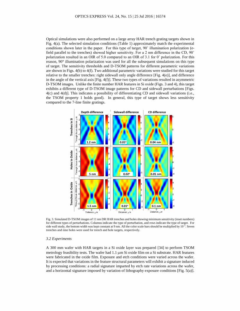
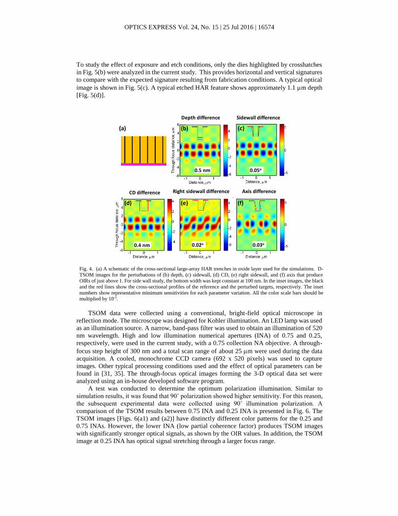
Optical simulations were also performed on a large array HAR trench grating targets shown in
Fig. 4(a). The selected simulation conditions (Table 1) approximately match the experimental
conditions shown later in the paper. For this type of target, 90˚ illumination polarization (e-
field parallel to the trenches) showed higher sensitivity. For a 2 nm difference in the CD, 90˚
polarization resulted in an OIR of 5.0 compared to an OIR of 3.1 for 0˚ polarization. For this
reason, 90° illumination polarization was used for all the subsequent simulations on this type
of target. The sensitivity thresholds and D-TSOM patterns for different parametric variations
are shown in Figs. 4(b) to 4(f). Two additional parametric variations were studied for this target
relative to the smaller trenches: right sidewall only angle difference [Fig. 4(e)], and difference
in the angle of the vertical axis [Fig. 4(f)]. These two types of variations resulted in asymmetric
D-TSOM images. Unlike the finite number HAR features in Si oxide (Figs. 3 and 4), this target
exhibits a different type of D-TSOM image patterns for CD and sidewall perturbations [Figs.
4(c) and 4(d)]. This indicates a possibility of differentiating CD and sidewall variations (i.e.,
the TSOM property 1 holds good). In general, this type of target shows less sensitivity
compared to the 7-line finite gratings.
Fig. 3. Simulated D-TSOM images of 11 nm DR HAR trenches and holes showing minimum sensitivity (inset numbers)
for different types of perturbations. Columns indicate the type of perturbation, and rows indicate the type of target. For
side wall study, the bottom width was kept constant at 9 nm. All the color scale bars should be multiplied by 10-3. Seven trenches and nine holes were used for trench and hole targets, respectively.
3.2 Experiments
A 300 mm wafer with HAR targets in a Si oxide layer was prepared [34] to perform TSOM
metrology feasibility tests. The wafer had 1.1 m Si oxide film on a Si substrate. HAR features
were fabricated in the oxide film. Exposure and etch conditions were varied across the wafer.
It is expected that variations in the feature structural parameters will exhibit a signature induced
by processing conditions: a radial signature imparted by etch rate variations across the wafer,
and a horizontal signature imposed by variation of lithography exposure conditions [Fig. 5(a)].
1.2 nm 0.01o 0.04 nm
5 nm 0.02o 0.05 nm
Depth difference Sidewall difference CD difference
1.5 nm 0.01o 0.1 nm
Tren
ches
in S
iH
ole
s in
Oxi
de
Tren
ches
in O
xid
e
OPTICS EXPRESS Vol. 24, No. 15 | 25 Jul 2016 | 16574
To study the effect of exposure and etch conditions, only the dies highlighted by crosshatches
in Fig. 5(b) were analyzed in the current study. This provides horizontal and vertical signatures
to compare with the expected signature resulting from fabrication conditions. A typical optical
image is shown in Fig. 5(c). A typical etched HAR feature shows approximately 1.1 m depth
[Fig. 5(d)].
Fig. 4. (a) A schematic of the cross-sectional large-array HAR trenches in oxide layer used for the simulations. D-
TSOM images for the perturbations of (b) depth, (c) sidewall, (d) CD, (e) right sidewall, and (f) axis that produce
OIRs of just above 1. For side wall study, the bottom width was kept constant at 100 nm. In the inset images, the black
and the red lines show the cross-sectional profiles of the reference and the perturbed targets, respectively. The inset
numbers show representative minimum sensitivities for each parameter variation. All the color scale bars should be multiplied by 10-3.
TSOM data were collected using a conventional, bright-field optical microscope in
reflection mode. The microscope was designed for Kohler illumination. An LED lamp was used
as an illumination source. A narrow, band-pass filter was used to obtain an illumination of 520
nm wavelength. High and low illumination numerical apertures (INA) of 0.75 and 0.25,
respectively, were used in the current study, with a 0.75 collection NA objective. A through-
focus step height of 300 nm and a total scan range of about 25 m were used during the data
acquisition. A cooled, monochrome CCD camera (692 x 520 pixels) was used to capture
images. Other typical processing conditions used and the effect of optical parameters can be
found in [31, 35]. The through-focus optical images forming the 3-D optical data set were
analyzed using an in-house developed software program.
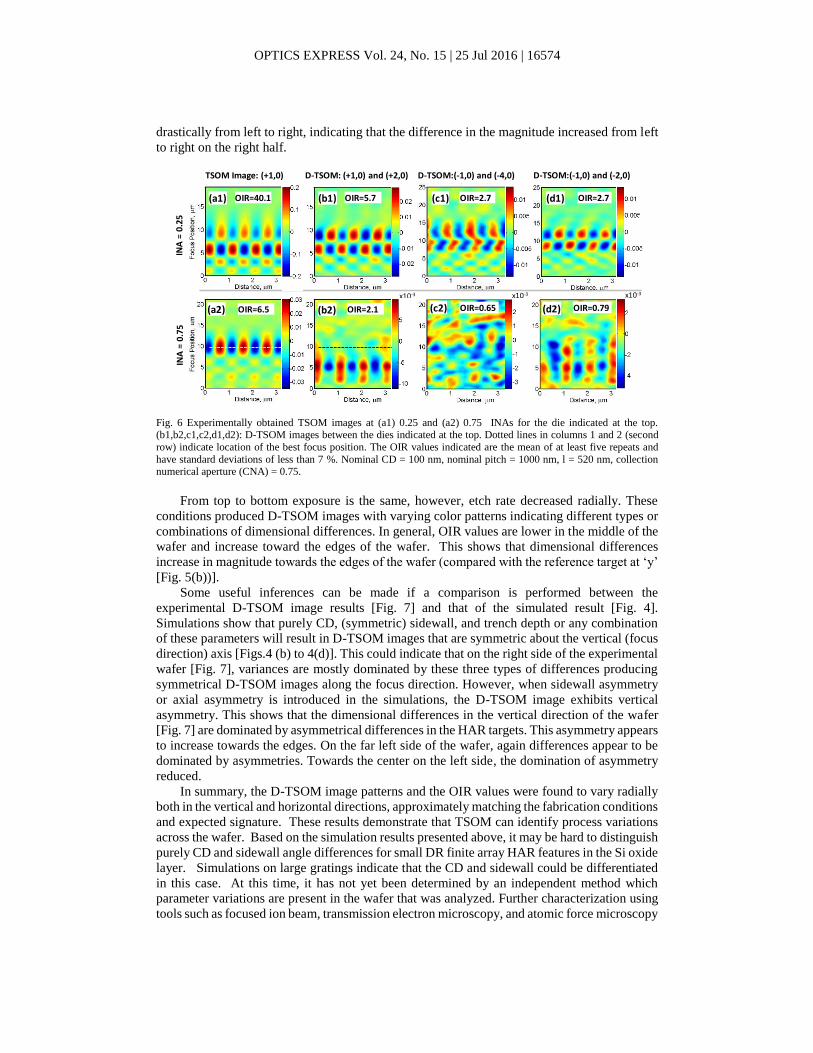
A test was conducted to determine the optimum polarization illumination. Similar to
simulation results, it was found that 90˚ polarization showed higher sensitivity. For this reason,
the subsequent experimental data were collected using 90˚ illumination polarization. A
comparison of the TSOM results between 0.75 INA and 0.25 INA is presented in Fig. 6. The
TSOM images [Figs. 6(a1) and (a2)] have distinctly different color patterns for the 0.25 and
0.75 INAs. However, the lower INA (low partial coherence factor) produces TSOM images
with significantly stronger optical signals, as shown by the OIR values. In addition, the TSOM
image at 0.25 INA has optical signal stretching through a larger focus range.
0.4 nm
0.5 nm 0.05o
0.02o 0.03o
CD difference
Sidewall differenceDepth difference
Right sidewall difference Axis difference
(a) (b)
(d) (e) (f)
(c)

OPTICS EXPRESS Vol. 24, No. 15 | 25 Jul 2016 | 16574
Fig. 5 (a) Exposure and etch conditions used to fabricate the HAR wafer. Exposure time increases from left to right.
Etching changes radially, being slower at the edges. (b) Row and column dies selected for analysis are shown by cross hatches. Dies marked by ‘x’ and ‘y’ are the reference targets used for the left half and the right half of the wafer,
respectively. The center die has a coordinate of (0,0). (c) A typical optical image of the selected HAR targets for
analysis. CD = 100 nm, PT = 1000 nm, = 520 nm, INA = 0.11, CNA = 0.75. (d) Dual-beam, focused-ion-beam cross-sectional SEM images of HAR holes in oxide showing depth.
Different INAs produce distinctly different D-TSOM images using the same set of targets,
as shown in column 2 [Fig. 6]. Similar to the TSOM images, the D-TSOM images show
stronger signal (higher OIR) for the 0.25 INA. This demonstrates that TSOM shows higher
sensitivity for HAR type of targets also at lower INAs (or at lower partial coherence factor
[36]).
It is often thought that the optical images (or information) acquired outside the best focus
range are not particularly useful. For this reason, much emphasis is given to determine the best
focus and then to acquire images at this focus position. However, the D-TSOM image [Fig.
6(b2)] shows no differential signal around the best focus position, which is indicated by a dotted
line. But it shows a strong differential pattern far away from the best focus position (on the
lower half of the D-TSOM image). This useful differential signal is lost if the analysis is done
near to the best focus position. TSOM facilitates accessing this type of useful optical signal
beyond the best focus position.
The D-TSOM image shown in Figs. 6(c1) and 6(c2) again emphasize the importance of
lower partial coherence factor. At the higher INA, the D-TSOM image appears noisy with no
particular color pattern, implying no discernible dimensional difference between the two targets
compared. However, at the lower INA, a clear color pattern with signal strength above the
noise level can be observed. This clearly shows a discernible dimensional difference that only
lower INA highlights [6].
Figs. 6(d1) and 6(d2) again show a stronger D-TSOM image pattern at the lower INA.
However, at the higher INA, the D-TSOM image shows a discernible color pattern, even though
its OIR of 0.79 is well below the noise level of one. This indicates a possibility of detecting
dimensional differences even below the noise threshold level conservatively fixed in the current
study at an OIR of one. It also suggests that the noise threshold level criteria could be lowered.
Since the results shown above clearly demonstrate superior performance of the lower INA,
only the results using 0.25 INA are presented in the following section.
A summary of TSOM image analysis performed along the horizontal and vertical
directions [Fig. 5(b)] is presented in Fig. 7. On the left half of the wafer, both exposure and etch
rate increased from left to right. D-TSOM image patterns on this part of the wafer show low
OIR values (red line). Similarly, not much variation in the OIR values can be observed.
However, D-TSOM image patterns change indicating different types of dimensional
differences. Low OIR values could also mean lower magnitude differences in dimension
(TSOM property 3). On the right half of the wafer, exposure increased but etch rate decreased
from left to right. This combination produced similar D-TSOM images. This may indicate
changes in similar target dimensions on dies in this row. However, their OIR values increased
10 m
m
(a) (b) (c) (d)
OPTICS EXPRESS Vol. 24, No. 15 | 25 Jul 2016 | 16574
drastically from left to right, indicating that the difference in the magnitude increased from left
to right on the right half.
Fig. 6 Experimentally obtained TSOM images at (a1) 0.25 and (a2) 0.75 INAs for the die indicated at the top. (b1,b2,c1,c2,d1,d2): D-TSOM images between the dies indicated at the top. Dotted lines in columns 1 and 2 (second
row) indicate location of the best focus position. The OIR values indicated are the mean of at least five repeats and
have standard deviations of less than 7 %. Nominal CD = 100 nm, nominal pitch = 1000 nm, l = 520 nm, collection numerical aperture (CNA) = 0.75.
From top to bottom exposure is the same, however, etch rate decreased radially. These
conditions produced D-TSOM images with varying color patterns indicating different types or
combinations of dimensional differences. In general, OIR values are lower in the middle of the
wafer and increase toward the edges of the wafer. This shows that dimensional differences
increase in magnitude towards the edges of the wafer (compared with the reference target at ‘y’
[Fig. 5(b))].
Some useful inferences can be made if a comparison is performed between the
experimental D-TSOM image results [Fig. 7] and that of the simulated result [Fig. 4].
Simulations show that purely CD, (symmetric) sidewall, and trench depth or any combination
of these parameters will result in D-TSOM images that are symmetric about the vertical (focus
direction) axis [Figs.4 (b) to 4(d)]. This could indicate that on the right side of the experimental
wafer [Fig. 7], variances are mostly dominated by these three types of differences producing
symmetrical D-TSOM images along the focus direction. However, when sidewall asymmetry
or axial asymmetry is introduced in the simulations, the D-TSOM image exhibits vertical
asymmetry. This shows that the dimensional differences in the vertical direction of the wafer
[Fig. 7] are dominated by asymmetrical differences in the HAR targets. This asymmetry appears
to increase towards the edges. On the far left side of the wafer, again differences appear to be
dominated by asymmetries. Towards the center on the left side, the domination of asymmetry
reduced.
In summary, the D-TSOM image patterns and the OIR values were found to vary radially
both in the vertical and horizontal directions, approximately matching the fabrication conditions
and expected signature. These results demonstrate that TSOM can identify process variations
across the wafer. Based on the simulation results presented above, it may be hard to distinguish
purely CD and sidewall angle differences for small DR finite array HAR features in the Si oxide
layer. Simulations on large gratings indicate that the CD and sidewall could be differentiated
in this case. At this time, it has not yet been determined by an independent method which
parameter variations are present in the wafer that was analyzed. Further characterization using
tools such as focused ion beam, transmission electron microscopy, and atomic force microscopy
OIR=40.1
OIR=6.5
OIR=5.7
OIR=2.1
OIR=2.7
OIR=0.65 OIR=0.79
OIR=2.7
INA
= 0
.75
INA
= 0
.25
x10-3 x10-3 x10-3
TSOM Image: (+1,0) D-TSOM: (+1,0) and (+2,0) D-TSOM:(-1,0) and (-4,0) D-TSOM:(-1,0) and (-2,0)
(a1) (b1) (c1) (d1)
(a2) (b2) (c2) (d2)

OPTICS EXPRESS Vol. 24, No. 15 | 25 Jul 2016 | 16574
is currently underway and will allow for the establishment of a correlation between OIR,
D-TSOM, and variation of the structural parameters of the trenches.
Fig. 7 Measured D-TSOM images approximately positioned at their respective locations on the wafer. Red (horizontal) and blue (vertical) curves show general trends in the OIR values in their respective directions and also represent their
color scale range. INA=0.25
TSOM has an inherent advantage over conventional optical imaging as it collects
substantially more 3-D optical information [25]. It is also capable of analyzing isolated targets
(as compared to scatterometry). This enables TSOM to simultaneously analyze several targets
or locations present in the optical field-of-view. In addition, substantially smaller grating targets
are sufficient for the TSOM metrology analysis, compared to the conventional 30 m to 50 m
square grating targets required for scatterometry analysis. The width of the grating targets used
in the current study did not exceed 0.5 m. To minimize the optical interference from the ends
of the line, the optimal length of the grating needed for TSOM analysis is about 10 times the
wavelength, i.e., about 5 m. Similarly, to minimize optical interference, it is best to have a
free space of about five times the wavelength on both sides of the target HAR features, i.e.,
about 2.5 m on each side. This results in an optimal target area that is over 50 times smaller
than a typical scatterometry target. The target area required for a lower wavelength such as 250
nm can be even smaller (over 100 times smaller). This potentially results in cost savings by
considerably reducing the real estate required for metrology targets. This may also improve
measurement accuracy by enabling the metrology targets to be placed in the active area of the
wafer (due to smaller areas needed). In addition, the present work demonstrates that TSOM can
be implemented using widely available, visible-wavelength, conventional optical microscopes.
This is an attractive metrology solution since it can easily be built, it is low-cost, and it has a
relatively high through-put. In comparison to the other semiconductor metrology tools, the
TSOM measurement time was considered “excellent”, on par with scatterometry [3]. Under
the optimized conditions the TSOM measurement time can be significantly less than 200 ms
[35,37], making it an attractive solution for high volume manufacturing. In addition, several
0
4.5
9.0
0 3.5 7.0 OIR
OIR
Distance, 2 mTh
rou
gh-f
ocu
s d
ista
nce
, 1
2
m
OPTICS EXPRESS Vol. 24, No. 15 | 25 Jul 2016 | 16574
targets located in a given field-of-view can be analyzed simultaneously from a single set of
through-focus data.
4. Conclusions
In this work we evaluated the possibility of using TSOM to detect 3-D shape variations present
in HAR features by making use of the three properties of D-TSOM images. We performed both
simulations and measurements using visible wavelength illumination. Simulations
demonstrated the ability of TSOM to detect nanoscale 3-D shape variations of HAR targets.
Sensitivity to sidewall angle of HAR features appears to be a strong capability of TSOM.
Simulated sensitivity obtained by TSOM either matches or exceeds ITRS requirements down
to the 11 nm node. Experimental TSOM result trends correlate with the expected variations
based on the fabrication conditions of the wafer. At this time, some broad inferences regarding
the shape of the HAR targets could be made based on the symmetries of the D-TSOM images.
TSOM might make an effective hybrid pairing with LL-BSE CD-SEM [33] for accurate HAR
measurements—the authors hope to see this further explored. These results suggest TSOM has
the potential to provide an economical additional capability for process control and yield
enhancement in high volume manufacturing, if throughput can be kept compatible with ITRS
requirements for bright field inspection (≈1000 cm2/hr).
Acknowledgments
Yuki Chiba, Timothy Gilday, and Akiteru Ko from Tokyo Electron were very helpful in
performing the HAR etch, and James Nadeau of FEI performed the cross-section of these
features. The authors also thank Hyeong-Gon Kang for miscellaneous help and the Summer
Undergraduate Research Fellowship (SURF) program of NIST and NSF for providing an
internship to Peter Weck.
Disclaimer: Certain commercial materials and equipment are identified in order to adequately
specify the experimental procedure. Such identification does not imply recommendation by the
National Institute of Standards and Technology (NIST) or by SUNY Polytechnic SEMATECH.
Related Documents