'~RADC-TR-88-321 ~-'Final Technical Report Vil Februar 1989 FAULT TOLERANT VLSI DESIGN USING ERROR CORRECTING CODES Syracuse University C.R.P. Hartmann, P.K. Lala, A.M. Ali, S. Ganguly, G.S. Visweswaran APPROVED FOR PUBLIC RELEASE; DISTRIBUTION UNLIMITED. 10 1 ROME AIR DEVELOPMENT CENTER Air Force Systems Command Griffiss Air Force Base, NY 13441 -5700

Welcome message from author
This document is posted to help you gain knowledge. Please leave a comment to let me know what you think about it! Share it to your friends and learn new things together.
Transcript

'~RADC-TR-88-321
~-'Final Technical ReportVil Februar 1989
FAULT TOLERANT VLSI DESIGN USINGERROR CORRECTING CODES
Syracuse University
C.R.P. Hartmann, P.K. Lala, A.M. Ali, S. Ganguly, G.S. Visweswaran
APPROVED FOR PUBLIC RELEASE; DISTRIBUTION UNLIMITED.
10 1
ROME AIR DEVELOPMENT CENTERAir Force Systems Command
Griffiss Air Force Base, NY 13441 -5700

This report has been r,,,:itwed bv the RADC Pub] ic Affairs )ivision (PA)and is releasable to the National Technical Information Service (NTIS). AtNTIS it will be releasable to the general public, including foreign nations.
RAPC-T-S- 2 1 ha c been rev iewod and is approved for piihl icat ion.
APPROVED:
KEVIN A. KUIATProject Engineer
APPROVED:
TOH J. BARTTechnical DirectorDirectorate of Reliability & Compatibility
FOPI THlE COM !ADER:
JAMIES U. HYDE, IIIDirectorate of Plans & Programs
If your address has changed or if you wish to be removed from the RADCmailing list, or if the addressee is no longer employed by your organization,please notify RADC (RBA )Griffiss AFB NY 13441-5700. This will assist us inmaintaining a current mailing list.
Do not return copies of this report unless contractual obligations or noticeson a specific document require that it be returned.

UNCLASSIFIEDSECURITY CLASSIFICATION OF THIS PAGE
Form ApprovedREPORT DOCUMENTATION PAGE OMB No. 0704-0188
'a REPORT SECURITY CLASSIFICATION I b. RESTRICTIVE MARKINGSUNCLASSIFIED N/A
IECURITY CLASSIFICATION AUTHORITY 3. DISTRIBUTION /AVAILABILITY OF REPORT
Approved for public release;2b. DECLASSIFICATION / DOWNGRADING SCHEDULE distribution unlimited.N/A
4 PERFORMING ORGANIZATION REPORT NUMBER(S) 5, MONITORING ORGANIZATION REPORT NUMBER(S)
N/A RADC-TR-88-321
6a. NAME OF PERFORMING ORGANIZATION 6b. OFFICE SYMBOL 7a. NAME OF MONITORING ORGANIZATIONSyracuse University (If appicable) Rome Air Development Center (RBRA)
6c. ADDRESS (City, State, and ZIP Code) 7b. ADDRESS (City, State, and ZIP Code)Department of Computer & Information Sciences Griffiss AFB NY 13441-5700
Syracuse NY 13244
Ba. NAME OF FUNDING/SPONSORING 8b. OFFICE SYMBOL 9 PROCUREMENT INSTRUMENT IDENTIFICATION NUMBERORGANIZATION (If applicable)
Rome Air Development Center RBRA F30602-81-C-0169
Sc. ADDRESS (City, State, and ZIP Code) 10. SOURCE OF FUNDING NUMBERS
Griffiss AFB NY 13441-5700 PROGRAM PROJECT TASK WORK UNITELEMENT NO. NO NO ACCESSION NO62702F 2338 01 PU
11. TITLE (Include Security Classification)
FAULT TOLERANT VLSI DESIGN USING ERROR CORRECTING CODES
12. PERSONAL AUTHOR(S)
C. R. P. Hartmann, P. K. Lala, A. M. All, S. Ganguly, G. S. Visweswaran13a. TYPE OF REPORT 13b. TIME COVERED 14. DATE OF REPORT (Year, Month, Day) 15 PAGE COUNTFinal FROM Mar 87 TO Mar88 February 1989 72
16. SUPPLEMENTARY NOTATION
N/A
17. COSATI CODES 18. SUBJECT TERMS (COntinue on revere if necenary and identify by block number)FIELD GROUP SUB-GROUP Fault Tolerant Error Correction Bus Circuits
09 04 Self-Checking Circuits Error Detection EDAC09 02 On-Chip Fault Microcircuits VLSI
19. ABSTRACT (Continue on reverse if necessary and identify by block number)Very Large-Scale Integration (VLSI) provides the opportunity to design fault tolerant, self-checking circuits with on-chip, concurrent error correction. This study determines theapplicability of a variety of error-detecting, error-correcting codes (EDAC) in high speeddigital data processors and buses. In considering both microcircuit faults and bus faults,some of the codes examined are: Berger, repetition, parity, residue, and Modified ReflectedBinary codes. The report describes the improvement in fault tolerance obtained as a resultof implementing these EDAC schemes and the associated penalties in circuit area.
20. DISTRIBUTION/AVAILABILITY OF ABSTRACT 21 ABSTRACT SECURITY CLASSIFICATIONrAUNCLASSIFIED/UNLIMITED 03 SAME AS RPT 3 DTIC USERS I UNCLASSIFIED
22a NAME OF RESPONSIBLE INDIVIDUAL 22b. TELEPHONE (Include Area Code) 22c. OFFICE SYMBOLKEVIN A. KWIAT (315) 330-2047 RADC/RBRA
DO Form 1473, JUN 86 Previous editions are obsolete. SECURITY CLASSIFICATION OF THIS PAGE
UNCLASSIFIED

EVALUATION
Very Large Scale Integration (VLSI) provides the opportunity to design fault tolerant
inicrocircuits that have on-chip, concurrent error correction. Long before VLSI,
error-correcting codes were used to provide error-free communication over noisy
channels. Digital memories used coding techniques to provide correct data in spite
of bit errors in stored data. By using techniques applicable to VLSI design and
appropriate fault models, this task evaluates the use of error-detecting and correcting
(EDAC) codes in high speed digital data processors and buses.
This report determines the applicability of a variety of EDAC codes such as: Berger,
repetition, parity, residue, and Modified Reflected Binary (MRB) codes. The
applicability of a code is determined by the demonstrated improvement in fault
tolerance obtained by a particular coding scheme and the concomitant penalty in chip
area or bus width needed to accommodate any redundant circuitry.
The results in this report substantiate the completeness of the evaluation. Although
no single fault-tolerant technique using EDAC codes is a complete solution, this study
provides the supporting data for making trade-off decisions.
Selecting a "best" technique for fault-tolerance that does not negatively impact
performance or throughput requires consideration of many factors. This task has
provided information that will allow intelligent consideration of EDAC codes as
design options.
KEVIN A. KWIAT
Project Engineer

Table of Contents
Section Page
1 Introduction 1
2 Self-Checking and Fault Tolerant Bus Design 3
2.1 Nature of Bus Faults 3
2.2 Design of Self-Checking Buses 4
2.3 Design of SEC-DED Buses 18
2.4 Conclusion 21
3 Design of Self-Checking Arithmetic Circuits 25
3.1 Duplicated Adder 25
3.2 Parity Prediction Adder 28
3.3 MRB Code Adder 31
3.4 Comparison of Adder Schemes 41
3.5 MRB Multiplier 42
3.6 Conclusion 44
4 Residue Codes 48
4.1 Error Detection using Residue Codes 49
4.2 Error Correction using Residue Codes 52
4.3 Conclusion 53
ii

5 Conclusion 55
Appendix 1 56
References 57
Accesqton For
N', TS C T'r7liIC TAB
Availability Codes
Aill and/or(
is Seca

List of Figures
Figure Page
1 Effective Model for a Short in a Bus 5
2 Block Diagram for Proposed Implementation 11
3 A Two Rail Checker ImplementaLion 12
4 Modified Scheme with Separate Buses for Information and
Check Bits 13
5 A Time Multiplexed Error Detecting Scheme for a Flat Bus 15
6 Timing Diagram for the Scheme Depicted in Fig.5 16
7 SED-DED Scheme 19
8 Check/Syndrome Generator 20
9 Correction Network 22
10 Decision Network 23
11 Circuit Diagrams for the Nonredundant Adder Cell 26
12 Layout of Nonredundant Adder Cell 27
13 Duplicated Adder Scheme 29
14 Layout of Duplicated Adder Cell 30
15 Parity Prediction Adder 32
16 Layout of Parity Prediction Adder Cell 33
iv

17 Example of MRB Addition 35
18 MRB Addition Scheme 38
19 Layout of MRB Adder Cell 40
20 Confidence Level of Adder Circuits 43
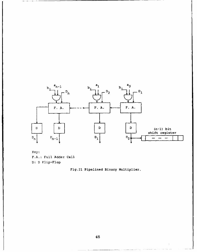
21 Pipelined Binary Multiplier 45
22 Pipelined MRB Multiplier 46
23 Residue Code Adder 50
24 Error Correction Using Biresidue Codes 54
V

Section 1. Introduction
The reliability of a circuit can be enhanced by employing the method of worst-
case design, using high quality components, imposing strict quality control pro-
cedures during the assembly phase, and using extensive testing. However, such
measures can significantly increase the cost. Furthermore, the effectiveness of these
techniques is reduced because it is not possible to exhaustively test a complex
circuit. Also, a transient fault would not be detected by these techniques. An alter-
native approach to improve the reliability is to incorporate self-checking facilities in
a circuit; this allows the circuit to react "on the fly" to internal failures. For a given
set of faults, a self-checking circuit either produces the correct outputs or indicates
that the outputs are incorrect.
A wide variety of codes is available for possible use in self-checking circuit
design, e.g., parity codes, Hamming codes, m-out-of-n codes, Berger codes, and
residue codes. However, different codes have different error-detecting capabilities.
In order to choose an error-detecting code for a circuit it is essential to know the
effects of the faults under consideration on the outputs of the circuit. In general,
a non-code word at the output of a self-checking circuit indicates the presence of a
fault in the circuit.
In Section 2 we consider two schemes for the detection of an error caused by a
single short in a 32-bit bus. The first scheme utilizes a modified form of the Berger
code and is implemented by cascading ROMs. The second scheme is based on the
time-multiplexing of information and tests vectors on the bus. As we will show, the
test vectors required depend on the physical characteristics of the bus. A scheme
for correcting a single bit error is also proposed.
Section 3 deals with the detection of single bit error in basic arithmetic oper-
ations, e.g., addition and multiplication. Three separate schemes for the design of
self-checking adders have been considered. The overhead in terms of chip area and
the fault detection capability of each scheme is evaluated. One of these schemes
is based on the MRB (Modified Reflected Binary) code. This code is also used to
design a self-checking pipcined multiplier.
Finally, Section 4 considers the application of a well-known code, the residue
code, for the detection and correction of errors in fixed point adders.
2

Section 2. Self-Checking and Fault Tolerant Bus Design
A bus consists of one or more lines which transfer information and electrical
power between the various components of a digital system. The concept of a com-
mon bus, carrying data from one part of a system to another is so obvious that it
is difficult to imagine a complex digital system without one. The overall reliabil-
ity of a bus-oriented system is heavily dependent upon the reliability of the bus.
One way to improve the reliability of a bus is to make it self-checking. Two such
schemes are proposed in this section. We assume that the system consists of only
fully-complementary CMOS devices and that there are inverter banks at both ends
of a bus.
Section 2.1. Nature of Bus Faults
Faults most likely to occur in a bus are those due to a bridging between two
or more lines of the bus and those due to a break in one or more lines of the bus.
We will restrict our attention to a single break (or open fault) and a single short
between any number of lines.
Study of this type of bridging fault in CMOS circuits [Hart, 1987] has shown
that these faults can produce WIRED-ANDing or WIRED-ORing effect depending
on the values of the lines which are shorted. Moreover, all the shorted lines assume
the same logical value; hence these faults produce unidirectional errors. If this were
not true we would need at least one 0 --* 1 transition and one 1 --+ 0 transition due
to the fault; however, this violates the requirement that all shorted lines assume
the same logical value as a result of the fault.
3
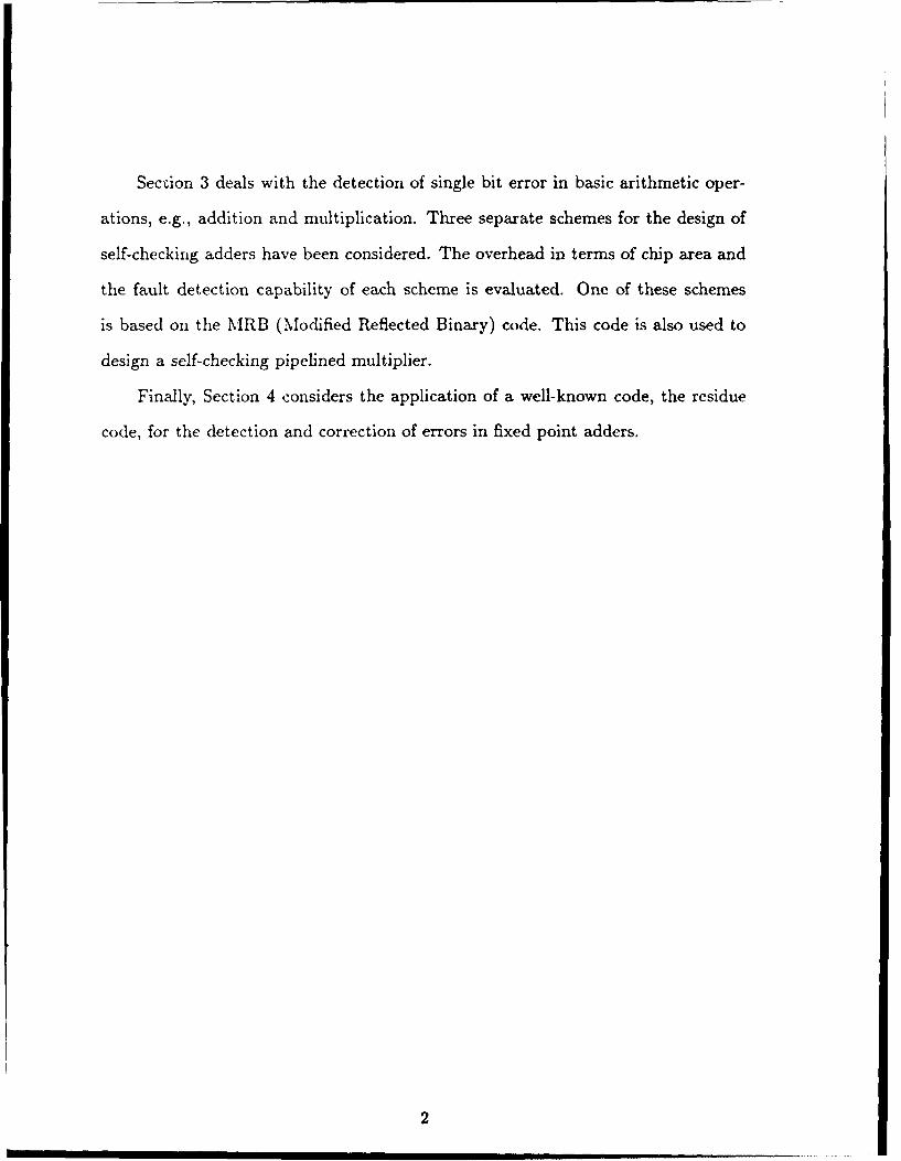
Consider a short between k lines of a bus. Let d denote the difference between
the number of ones and zeros in these k-bits, i.e.,
d = (number of ones) - (number of zeros).
This short can be modeled as shown in Fig. 1 where R. is the on-resistance of a
PMOS transistor, RN is the on-resistance of an NMOS transistor, and Vs is the
resultant voltage at the shorted lines. For Idl : k
Vs 1
SRN ./~k-id/
( R ) 2k
and 6 (Vs/VDD) RN (k+d) 2 >0.6(d) (i+ (Rp) (k-d)) 2
Vs is a monotonically increasing function of d; hence the value of d which decides
whether Vs is logic high or low would depend on k, Rp and RN. Thus the maximum
number of unidirectional errors also depend on k, Rp and RN. Simulation results
for values of k up to 8 show that the maximum number of unidirectional errors
is [§ + 11. Generally, for values of d which are not close to zero and for typical
values of (R-), the zeros of the shorted lines get converted to ones if the number
of ones is greater than the number of zeros, and vice versa. This implies that, in
this situation, the short can be modeled as a majority function.
Section 2.2. Design of Self-Checking Buses
For any bus to be self-checking it should at least be able to detect unidirectional
errors. To design an efficient scheme to make the bus self-checking we need to
investigate the effect of unidirectional errors. A unidirectional error always changes
the number of ones (or zeros) in the information present on the bus lines.
4

VS
2 aN
Fig.1 Effective Model for a
Short in a Bus.

Consider a k-bit bus. We can define a partition 7r on the set of the 2 k possible
data words. This partition has k + 1 blocks where data words containing the same
number of ones (or zeros) belong to the same block of ir. This is illustrated in Table
1 where block B, contains all data words with i ones. Since a unidirectional error
always changes the count of ones, it can never erroneously convert a data word to
another belonging to the same block of ir. Thus, to detect unidirectional errors, we
can append the same check bits to data words which have the same number of ones,
and from now on we only need to consider data words shown in Table 1.
Block Data
B0 000 ............... 000B1 000 ............... 001B 2 000 ............... 011
Bk 111 ............... 111
Table 1.
We now formalize the above concepts. Let X and Y be two binary k-tuples.
Definition 1. The Hamming distance between X and Y, D(X, Y), is defined as
the number of bit positions in which they differ.
Definition 2. The crossover from X to Y, N(X, Y), is defined as the number of
bit positions in which X is 1 and Y is 0.
Example:Let X = 10011010 and
Y = 00110111.
Then D(X, Y) = 5, N(X, Y) = 2, and N(Y, X) = 3.
6

Note that D(X, Y) = N(X, Y) + N(Y, X). The following theorem gives the
conditions required for a code to detect t unidirectional errors.
Theorem 1 [Bose,1985]. A code C is capable of detecting up to t unidirectional
errors iff for all distinct codewords X and Y belonging to C at least one of the
following conditions is satisfied:
(i) D(X,Y) > t + 1;
(ii) N(X,Y) > 1 and N(Y,X) > 1.
Note that all binary tuples of the same block of 7r satisfy condition (ii) of
Theorem 1.
Let us now obtain a lower bound for the number of check bits required by a
separable code to detect t-unidirectional errors. Separable codes are those in which
no decoding is required to extract the information bits from the codeword. Using
condition (i) of Theorem 1 we can assign the same check bits to two blocks B, and
Bj of ir (without loss of generality assume i < j) whenever j-i > t+1. Thus we can
assign the same check bits to blocks Bi and Bi+t+l for i = 0, 1, 2,... (k - t - 1). As
a consequence, only blocks B0 through Bt need to be assigned distinct check bits.
Therefore, the lower bound for the number of check bits required by a separable
code to detect t unidirectional errors is [log2 (t + 1)]. For t = k the lower bound for
the number of check bits is [log 2(k + 1)].
Berger has proposed a technique to design a separable code, using [log2 (k + 1)1
check bits to encode k information bits, capable of detecting all unidirectional errors
[Berg, 19611. Thus Berger codes are optimum.
We are interested in designing a separable code for a bus with 32 information
bits. As discussed earlier, we expect to have not more than t = r[ + 1] = 17
unidirectional errors. Thus the number of check bits r has to be at least
7

[log 2 (17 + 1)1 = 5. The number of lines in the redundant bus is n = k + r. We now
propose a scheme that will detect all unidirectional errors caused by a single short
in a 37-bit bus consisting of 32 information bits and 5 check bits. Since in a bus
with 37 lines we expect to have at most [ + 1] = 20 unidirectional errors, this
scheme uses the minimum number of redundant bits required by a separable code.
Our scheme is a modification of that proposed by Berger [Berg, 1961]. In the
latter, the check bits are formed by taking the complement of the binary represen-
tation of the count of the ones in the information bits. For k = 32 the Berger code
requires 6 check bits. We notice that all information vectors except the all-i vector
have the same MSB (most significant bit) in the check bit part of the code. We
now delete this bit. We change the check bits for the all-1 information vector and
for the information vectors with 31 ones to 00000 and 10000, respectively. These
correspond to the last two rows of Table 2.
32 information bits 5 check bits
0 ..................... 0 1 1 1 1 10 ..................... 01 1 1 1 1 00 ..................... 011 1 1 1 0 1
17 15
0 ......... 0 1 ......... 1 10 0 00
001 ..................... 1 0 0 0 0 101 ..................... 1 1 0 0 0 011 ..................... 1 0 0 0 0 0
Table 2.
8

Notice that information vectors which have 31 ones and 15 ones have the same
check bits. Moreover, only the code words corresponding to these information
vectors do not satisfy condition (ii) of Theorem 1. These code words, denoted by
X and Y, are shown below where the check bits are given in parentheses:
X 0000 0000 0000 0000 0111 1111 1111 1111 (10000)
Y 0111 1111 1111 1111 1111 1111 1111 1111 (10000)
We must now show that a single short cannot change X to Y and vice versa.
Note that X has 21 zeros and 16 ones and Y has 5 zeros and 32 ones. To change X
to Y, 16 zeros have to be shorted with a certain number of ones (say m) to result in
a total of 32 ones. Notice that m < 16. The resultant voltage at the shorted lines,
Vs, caused by shorting 16 zeros with m ones is
YD
1+ (R) (16)where Rp and RN are the on-resistances of a PMOS and an NMOS transistor,
respectively. Note that Vs is an increasing function of m. Thus to obtain the
maximum value of Vs we choose m = 16; however, since Rp is typically 2 to 2 - 5
times RN, the resultant Vs is still logic low. Thus a single short cannot change X
to Y. By a similar analysis it can be shown that a single short in Y cannot change
16 ones to zeros, and hence Y can never change to X.
Consider a code word Z from the coding scheme shown in Table 2. Let Z be
different from X or Y defined earlier. No unidirectional error, irrespective of its
length, can change Z to another valid code word W belonging to Table 2 since
N(Z, W) >_ 1 and N(W, Z) _ 1. Thus the proposed coding scheme will detect the
errors caused by any single short in the 37 (= 32 + 5) bit bus. Fig. 2 shows a block
9

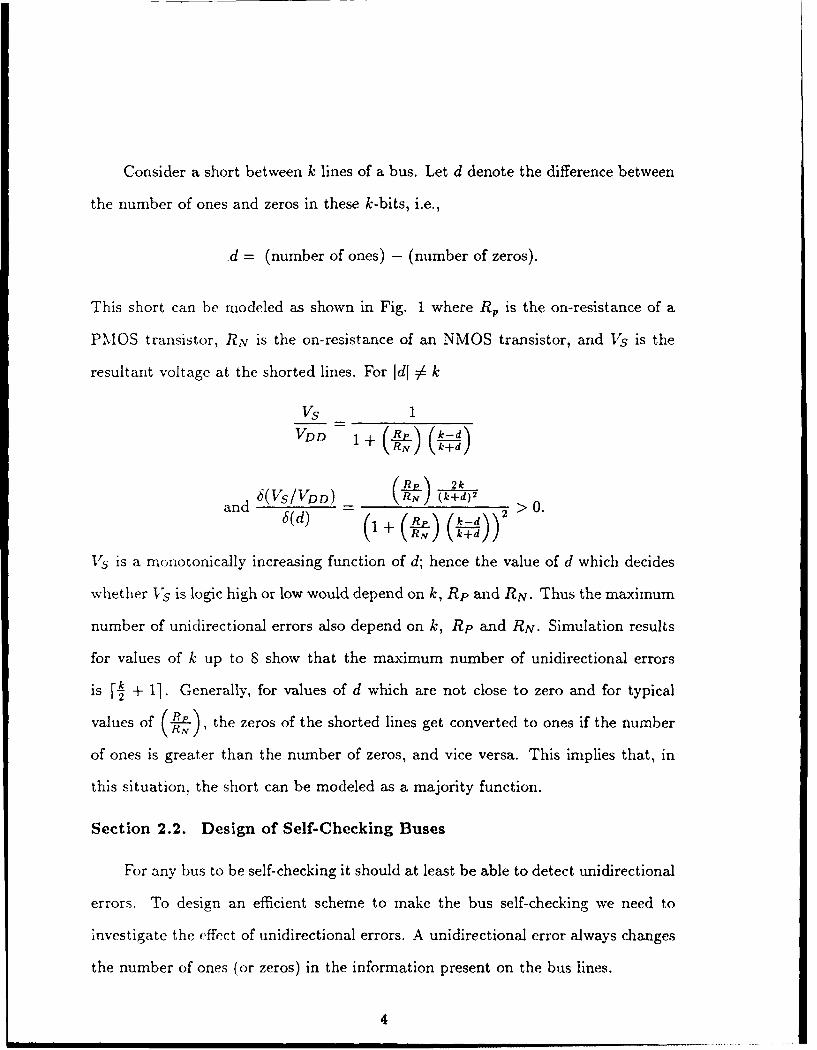
diagram for the proposed implementation. In this figure C(X) denotes the check
bits corresponding to the information vector X. Notice that ROM A and ROM
B give complementary output values for the same input. This enables us to use
a totally self-checking two-rail checker [Lala, 1985] to compare the ROM outputs.
There are many possible ways, including the use of PLAs, to implement the two-
rail checker [Lala, 1985]. Fig. 3 shows one possible implementation of the two-rail
checker.
According to our earlier analysis, any error produced by a single short in the
bus will be detected; moreover, since a single error is a trivial case of a unidirectional
error, any fault that produces a single error in the bus, e.g., a single line stuck open,
will be detected. Moreover, the two-rail checker is totally self-checking with respect
to all single stuck-at faults. Let us now consider faults in the ROM. These can be
classified into two categories:
(i) Faults for which there exists an input X that causes ROM
A (or B) to output C(Y) where C(Y) # C(X).
(ii) Faults for which there does not exist any input X that causes
ROM A (or B) to output C(Y) where C(Y) 0 C(X).
For the former category, in the absence of any other error, the two-rail checker
will detect the error caused by the ROM. Note that the latter category constitutes
an undetectable fault; however, even in the presence of such an undetectable fault
any fault which causes a unidirectional error in the bus is still detectable. The
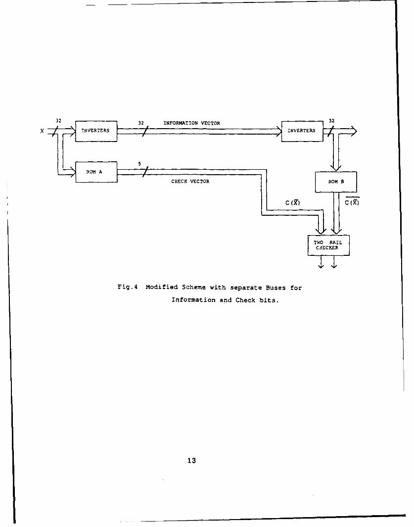
above scheme can be modified to one in which the information and check bits are
transmitted on two physically separate buses. The block diagram for this is shown
in Fig. 4; however, this does not detect all errors caused by separate single shorts
in both buses.
10

XINVERTERS x3
37 BI BUS NV CR E C E
110)
x1Yi X2 Y2 X3 Y3 X4Y4 X5 Y5 Xi
Variables Output ofX1,X2X3X4XS ROM AL
S1y2Y3 y4 y51 ROM B Y1 ___
(a) Design of a 5 input pair two (b) Gate level representation of a
rail checker using 2 input two input pair two rail checker.pair checker blocks.
Fig.3 A Two Rail Checker implementation.
12
x !NVERTERS NETR
CH~ECK VECTORRO8
TWO RAILCJECKER
Fig.4 Modified Scheme with separate Buses for
Information and Check bits.
13
Another possible strategy is to use the same 32-bit bus to transmit the infor-
mation and test vectors. These test vectors are inputs that detect single shorts in
the bus. The feasibility of this time-multiplexed scheme would depend on whether
the bus is physically "flat" or not. We define a "flat" bus as one in which a short
between any two lines always shorts these lines with all the lines physically located
between them.
Flat Bus
For a flat bus a single test vector consisting of alternating O's and l's (i.e.,
0101... 01) is sufficient to detect all errors due to single shorts in the bus. This is
because a single short would cause all the shorted lines to transmit all zeros or all
ones and hence the error can be detected.
Fig. 5 shows a possible implementation of this scheme. The control input S
of the multiplexer selects the information vector when S = 0 and the test vector
when S = 1. The input L is used to ensure that only the test vectors are latched
into the flip-flops. Fig. 6 shows the timing diagram for the operation of one cycle
of this scheme. For the scheme to be feasible it must satisfy the constraint
1T > m + tb + tFF + tc.F
Using Schottky TTL components we estimate that tn = 5ns, tFF = 5ns and
tc = 20ns. Therefore, systems with a clock rate of 25 MHZ and buses with delay
of 8ns or less would operate correctly. We note that this scheme would not detect
certain stuck-at faults. If time constraints permit, we can transmit the test vector
and its complement. This will enable us to increase the error-detecting capability
to include single stuck-at faults in the lines of the bus and at the output of the D
flip flops.
14

InformationVector 32 BITTest 2 :1 MUX 32 BIT BUS Otu
Vector
L D FLIP FLOPS
S
CHECKER
CIRCUIT
Fig.5 A Time Multiplexed Error Detecting Scheme for a Flat Bus.
15

1/F
ttrn
BusInpt_ _C ESTVETORINF~k I FMTON VECTOR
Bus Output
Output of Flip-flopstF
Output of
Checker
KEY:
tm :Multiplexer Delay
h :Bus Delay
tFF:Fip-flop Delay
tC :Checker Circuit Delay
F :Frequency of System Clock
Fig.6 Timing Diagram for the Scheme depicted in Fig.5
16

Non-Flat Bus
Since the bus is not flat, any two lines may be shorted together. To be able
to detect a single short between any two lines we must apply a test vector which
transmits different values on these two lines of the bus. Thus, to detect all possible
single shorts between any two lines we must transmit a set of test vectors such that
for any given pair of lines we have at least one test vector which transmits different
values on this pair of lines. This test set will also detect all possible single shorts
because for a short across any given t lines there exists at least one test vector in
this set which does not transmit the same value on these t lines.
Theorem 2. Let S be a set of vectors of length n. The members of S are such
that for all possible integral values of i and j, i # j and 1 < ij < n we can find
at least one vector in S which differs in its ith and jth component. Under these
conditions the cardinality of S > [log 2 n].
Proof. Consider the two-dimensional array where each row of the array consists
of one element of S. It is necessary that every two columns of the array be distinct
so that it satisfies the required condition. The minimum number of rows required
to get n distinct columns is [log 2 ni. a
For n = 32, consider a two-dimensional array whose columns consist of all the
32 distinct 5-tuples. The rows of this array form a set of test vectors with minimum
cardinality which satisfy the condition of Theorem 2.
If we want to implement a time-multiplexed scheme for a 32-bit non-flat bus,
we have to transmit 5 test vectors for every information vector. For a system clock
of 25 MHZ it is not possible to meet the timing constraints involved in transmitting
six vectors in one clock cycle. However, we could transmit a different test vector in
five consecutive clock cycles.
17

Section 2.3. Design of SEC-DED Buses
We are now interested in designing a scheme for single error-correcting (SEC)
and double error-detecting (DED) buses. We assume that the bus is the only source
of errors. Hsiao has proposed a class of SEC-DED codes [Hsia, 1970]. In order to
design a SEC-DED scheme for a 32-bit information bus we use the (39,32) SEC-
DED code constructed by Hsiao. The parity check matrix H for this is shown in
Table 3.
111111110000001000010010100000111000000000010011111111100100100100001000100000000100000001000011111111001101100010000
H= 001000100010010110000000111111110001000011001010100100100001111011010000000100100001101000111011111000000010000000010110110001111000001000001010100010000001
Table 3. Parity Check Matrix
Fig. 7 shows a possible implementation of the SEC-DED scheme. The Check
Generator generates the seven check bits from the information bits to be transmit-
ted on the bus in accordance with the parity check matrix. These seven bits are
transmitted in a separate bus. The Syndrome Generator first generates the check
bits corresponding to the information bits DO-D31 received at the output of the bus.
It then compares these check bits with the received check bits transmitted by the
7-bit bus and generates the 7 syndrome bits S1 through S7. The structure of one
of the seven cells that constitute the Check/Syndrome Generator is shown in Fig.
8. The Check Generator generates the check bit Cl. It does not contain gate G.
The Syndrome Generator consists of the Check Generator and gate G. It generates
the Syndrome bit S1 by comparing the received check bit C l with the check bit C1
18

Do-033
CHE CK BU SS Y D O EB B3GENERATOR / GENERATORB0-B3
-$7 -- ERROR
LOCATOR
DECISION _ Error Detected
-----KSingle ErrorDouble Error
Fig.7 SEC-DED Scheme.
19

0
1
2TD
22
24
19
22
Fig.8 Check/Syndrome Generator.
20
generated from the received information bits DO - D31. It can be easily shown that
if there is a single error in the information bus, then exactly three syndrome bits will
be 1. Moreover, if there is a single error in the transmitted check bits, then only one
syndrome bit will be 1. It can also be shown that an even number of errors results
in an even number of ones in the syndrome bits. Based on these properties, the
Error Locator can be implemented by using 32 three-input AND gates as shown in
Fig. 9. If there is a single error in bit i, Di, of the received information vector, then
the error locator would cause Bi to be 1 and all other outputs to be 0. Accordingly,
the Error Corrector consists of 32 two-input EX-OR gates as shown in Fig. 9.
The purpose of the Decision Network shown in Fig. 7 is to detect the presence of
correctable errors. It examines S1 through S7 and indicates whether A0 through
A31 should be accepted as correct information. If it flags a single error or no error
detected, then A0 through A31 is equal to AO through A31 given that, at most,
one error has occurred. If it flags double error, then Ao through A31 should not be
accepted since an even number of errors has occurred. An implementation of the
Decision Network is given in Fig. 10.
Section 2.4. Conclusion
In this section two schemes have been proposed to detect errors caused by a
single short in a 32-bit bus. The first scheme is based on a modified form of the
Berger code. The check bits are generated from the 32 information bits by using a
number of ROMs. The proposed scheme requires a tree of ROMs because a 32-bit
address ROM is not commercially available. While cascading the ROMs in a tree
structure care must be taken to ensure that the timing constraints of the system
are met.
21

Si-S7 DO D31
SI. BO
S7-I
s5S7-
Corrected* output
D31
S4. B31 - ---- A3 1
ERROR LOCATOR ERROR CORRECTOR
Fig.9 Correction Network.
22

S1
S2
S3 ____ Tree of
S4~ ErrorS 5 ____OR Gates Detected
S6S7 Double
Error
SingleError
Fig.lO Decision Network.
23

The other scheme considered for detecting a single short in a 32-bit bus is to
time-multiplex both the information bits and the test vectors on the bus. If the
bus is "flat," then the test vector basically consists of alternate O's and l's. For
a non-flat bus, to detect all possible single shorts between any two lines we must
transmit a set of test vectors such that for any given pair of lines we have at least
one test vector which transmits different values on this pair of lines. For an n-bit
bus we need at least [log 2 n] test vectors and it is therefore impractical to transmit
these vectors in one clock cycle.
Finally, a scheme for correcting a single-bit error and simultaneously detecting
a double-bit error in a 32-bit bus is also proposed.
24

Section 3. Design of Self-Checking Arithmetic Circuits
In this section we study several schemes for the design of self-checking adders.
Each scheme was evaluated by studying its fault coverage and comparing its area
requirements to those of a non-redundant adder. VLSI layouts were generated and
simulations were performed to verify the correctness of design for all the schemes.
The adder schemes studied were:
(i) Duplicated Adder;
(ii) Parity Prediction Adder [Prad, 1986];
(iii) MRB (Modified Reflected Binary) Code Adder [Luca, 1959].
Furthermore, we also discuss how a self-checking multiplier can be designed
using the MRB adder cell.
A fully complementary MOS non-redundant adder cell has been used for com-
parison of area requirements of the various schemes. Also, the duplication and
parity prediction adder cells were built using this cell. The logic equations for the
non-redundant adder cell are
si = ai E bi ( ci
Ci+l = aibi + ci(ai + bi).
Where ai and bi are the input bits to be added, ci is the input carry from the
previous stage, and si and ci+j are the sum and carry outputs, respectively. The
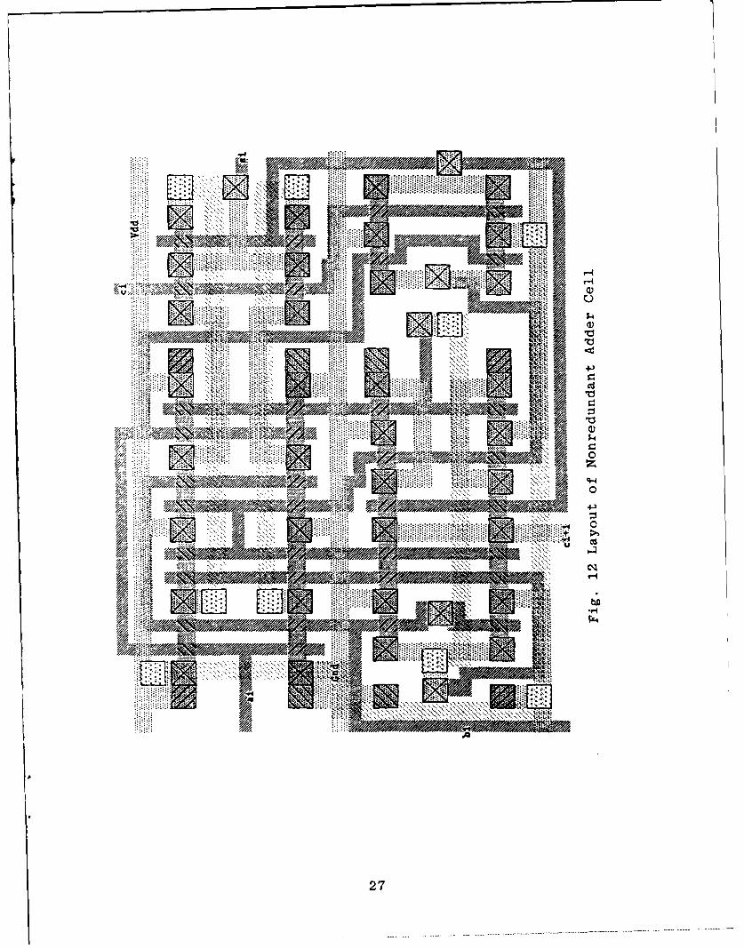
circuit diagrams and the layout used to design the non-redundant adder cell are
given in Figs. 11 and 12, respectively.
Section 3.1. Duplicated Adder
Duplication is a well known method used for purposes of fault detection. The
output of a circuit and its duplicate copy are compared to detect the presence of
errors. In the case of an adder, the si (sum) output of each cell and its duplicate
25

VvV
ddd
ii
Fig.ll Circuit Diagrams for the Nonredundant Adder Cell.
26
1 M4
'WRVN k.MI
010
IMP/
I -//
27

version are compared using an EX-OR gate. A tree of OR gates can now be used
to propagate an error signal indicated by one or more EX-OR gates. This method
would not detect several single stuck-at faults, e.g., any stuck-at-0 fault at the
output of an EX-OR gate. In order to overcome this deficiency, we propose a
duplication scheme which uses a totally self-checking two-rail checker to detect
errors in the adder. An implementation of our scheme for an n-bit adder is shown
in Fig. 13. Note that the inputs and outputs of the duplicate version of each cell are
complements of those of the original cell. This allows us to use a two-rail checker. All
single stuck-at faults except those at the primary inputs (which cannot be detected
by any scheme) can be detected by this scheme. The layout for a composite cell,
consisting of a non-redundant adder cell, its complementary version, and a two-rail
checker cell, is shown in Fig. 14.
Section 3.2. Parity Prediction Adder
In this section we study the parity prediction adder proposed by Tohma [Prad,
1986]. This scheme requires the parity bits for the numbers to be added. We assume
that these parity bits are already available. Let
a (an-1 an-2,..., a0,ap) and
b =(bn-1, bn-2 ,... bo, b,)
be two n-bit numbers along with their parity bits ap and bp. The result of adding
the n-bit numbers is
S = (Cn, Sn-1,...,0)
where c, is the carry-out from the last bit position. The parity bit for s is sp where
P = C ED s-1 ED s-2 ED Dso.(1)
28

b fn- 1 bn1 a. 0a bo
C 2 CNNRA
N R A N o n r e d u n d a n
T : ToRai TRCj rni 1 b1 jC
Checer Cell
Fig.13 Duplicated Adder Scheme.
29

-cil!IMzSR1RMv_
g--NIN't Ilk.. ........ I ... .I_<I RNMN NoMNI MR g
Is"55; M-3,
001 1\i-Wf , IN MIZqg M
.
.........IMM AN............." ......... ..
w m INm...... ..........
INN I . ...... go.............. HS W\
IN mmmm.z kw kMl
MIN'045-M."Z. 0P z SIMIIg g\g"mill IN
LN . 'm ................... I. .. .... ......... ........................................... ...... ............... ......................... .................. ...................... -j---'--'----! ...... ME\HIM M
M \1 INNO MR mMR:M NO "a, M\N M N II-KT III INNM &
gkg mm W.IMM
........... ....... . .......0 -7-1-1-1--x ..............nN, 'Eff .........ON m I.L.1 .......... .. INK ................. ......
mME AN'11 INN mg, g Im
.... ft w . I . ......... .......... ..................... ........ ....... ........................... ....................... .. . .....
...................... .......................................... ....... ... . ......
... ... .... ................ .N
.............. ............................ . ..
........................ ...... V.
.... ........... T 7..........vON
....................... % ........................ ...............t j, ........ . ....... .......... .......... ........ .... ..... 0 .......... ... I .............M .. ................ ...... .... .....
M\; S% jgk gg 'g m...... Am MN IN
i X-R,Eib' il. M-N, L -A gR15 : . r -;,t \ IM" . g & ,A, "mAn-; m .........
tv IN \:-:::W \g
.7 , .... ........I \ I \ - . ... .... II MIN ............ 11 ...1. .. .0 11 . ONmm km -- RX- *%,:
m ff
Ism
-" A , . *1 ' r ,. . . t.;. .: ... RN.... ... ...... .%
mx P. R T g.1.1.1:.I. xOP M 1 ......"'s ......... n MOMM MOSM.I. .....m . % r. -1,11"Mmm mmmsm I!FI ... . ................. .. *.*............................................. .................. ....................... ............
100 INm IN nRr R-On
0.4 a t . ......... MRMN
.. ........... .. mV.1.1.1.* . ...... .............. .... ......... . ............................... ................ ...... W
X z F:
FEDlam w era.... I IS.......... ZI ................................ ................. ------ . ...... .... ... z..... ..... M
*-'.1.7 . ....... ........ ............ ..........b ......
4W . ...............-------- - -------C
Fig. 14 Layout of Duplicated Adder Cell
30
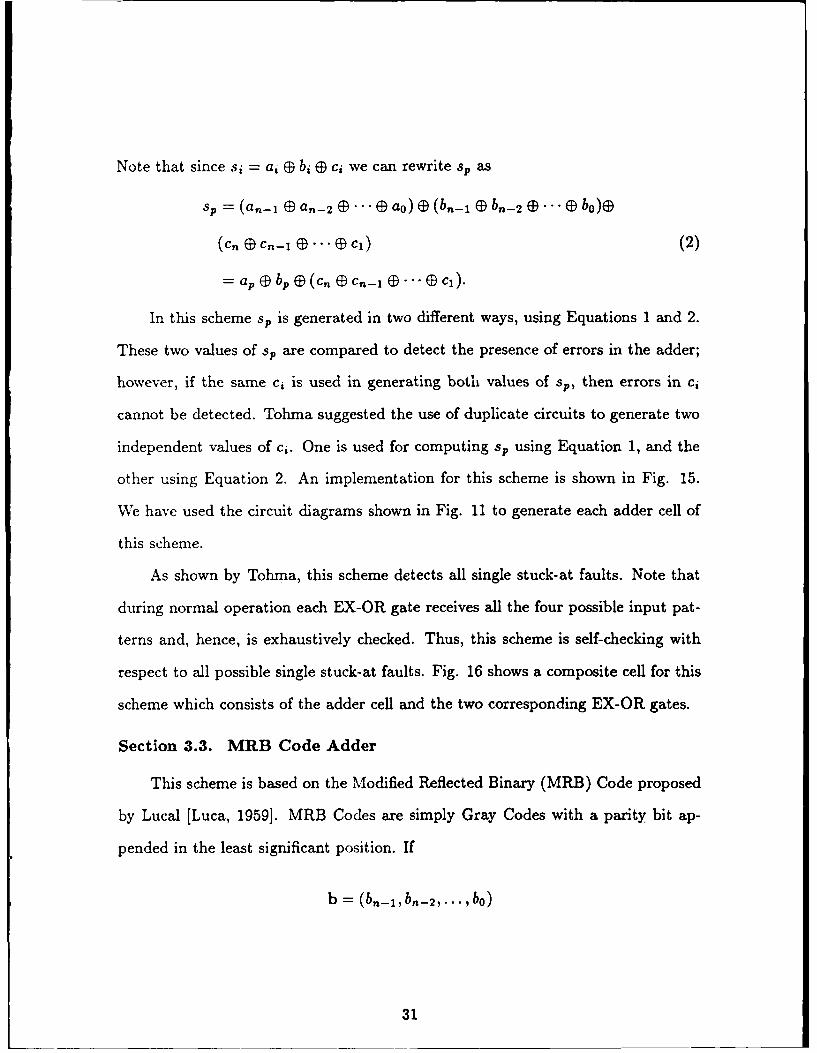
Note that since si = ai E bi ED ci we can rewrite sp as
sp = (an-i D an-2 E--- E a0) E (b.-I E b.-2 ED . b0)E
(c ecn_ E... eci) (2)
= p E) bp (D (c, ED c,- G)"- (D ci).
In this scheme sp is generated in two different ways, using Equations 1 and 2.
These two values of sp are compared to detect the presence of errors in the adder;
however, if the same ci is used in generating both values of sp, then errors in ci
cannot be detected. Tohma suggested the use of duplicate circuits to generate two
independent values of ci. One is used for computing sp using Equation 1, and the
other using Equation 2. An implementation for this scheme is shown in Fig. 15.
We have used the circuit diagrams shown in Fig. 11 to generate each adder cell of
this scheme.
As shown by Tohma, this scheme detects all single stuck-at faults. Note that
during normal operation each EX-OR gate receives all the four possible input pat-
terns and, hence, is exhaustively checked. Thus, this scheme is self-checking with
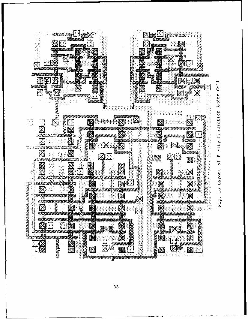
respect to all possible single stuck-at faults. Fig. 16 shows a composite cell for this
scheme which consists of the adder cell and the two corresponding EX-OR gates.
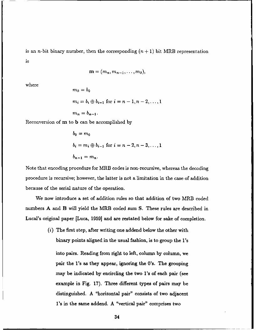
Section 3.3. MRB Code Adder
This scheme is based on the Modified Reflected Binary (MRB) Code proposed
by Lucal [Luca, 1959]. MRB Codes are simply Gray Codes with a parity bit ap-
pended in the least significant position. If
b = (b-I1bn-21,... ,bo)
31

sp1
c 2
Fig 15 Pait Prdc2 Ader
Cn ~3C
I 0 13 ~I
off ,.~~f'rX,.t ~ .,-
'suit.
I -0V=/
M, TUN
.
ITMAA
933
is an n-bit binary number, then the corresponding (n + 1) bit MRB representation
is
m = (man, ran-.... , MO),
wherem0 = bo
rmi -- bi (Dbi-1 for Z' = n - 1, n -2,.,
mn = bn-1.
Reconversion of m to b can be accomplished by
b0 - m0
bi =mi Ebi-1 for i = n-2,n -3,...,1
bn-1 = mnn.
Note that encoding procedure for MRB codes is non-recursive, whereas the decoding
procedure is recursive; however, the latter is not a limitation in the case of addition
because of the serial nature of the operation.
We now introduce a set of addition rules so that addition of two MRB coded
numbers A and B will yield the MRB coded sum S. These rules are described in
Lucal's original paper [Luca, 1959] and are restated below for sake of completion.
(i) The first step, after writing one addend below the other with
binary points aligned in the usual fashion, is to group the l's
into pairs. Reading from right to left, column by column, we
pair the l's as they appear, ignoring the O's. The grouping
may be indicated by encircling the two l's of each pair (see
example in Fig. 17). Three different types of pairs may be
distinguished. A "horizontal pair" consists of two adjacent
l's in the same addend. A "vertical pair" comprises two
34

A 00 11 10 1 23
1 011-57
1
SPartial Sums
S 1 1 110 0 00 80
Fig.17 Example of MRB addition.
35
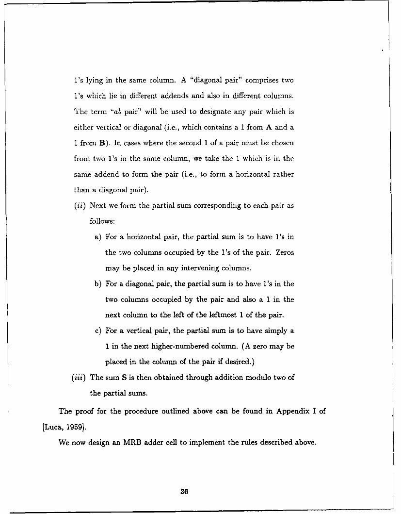
l's lying in the same column. A "diagonal pair" comprises two
l's which lie in different addends and also in different columns.
The term "ab pair" will be used to designate any pair which is
either vertical or diagonal (i.e., which contains a 1 from A and a
1 from B). In cases where the second 1 of a pair must be chosen
from two l's in the same column, we take the 1 which is in the
same addend to form the pair (i.e., to form a horizontal rather
than a diagonal pair).
(ii) Next we form the partial sum corresponding to each pair as
follows:
a) For a horizontal pair, the partial sum is to have l's in
the two columns occupied by the l's of the pair. Zeros
may be placed in any intervening columns.
b) For a diagonal pair, the partial sum is to have l's in the
two columns occupied by the pair and also a 1 in the
next column to the left of the leftmost 1 of the pair.
c) For a vertical pair, the partial sum is to have simply a
1 in the next higher-numbered column. (A zero may be
placed in the column of the pair if desired.)
(iii) The sum S is then obtained through addition modulo two of
the partial sums.
The proof for the procedure outlined above can be found in Appendix I of
[Luca, 1959].
We now design an MRB adder cell to implement the rules described above.
36

The basic adder cell operates on two digits at a time-the two digits of A and
B lying in a single column, beginning with the rightmost column. The information
which must be passed along from one column to the next (that is, from one basic
adder cell to the next) concerns the pairing of the l's and the partial-sum carry to
the next column when an ab pair is completed. This information may be conveyed
by two binary digits, which we denote E and F.
Fig. 18 shows the block diagram of an MRB adder. We assume that we have
to add two n-bit binary numbers so the corresponding MRB representations have
n + 1 bits; therefore, the resultant sum contains, at most, n + 2 bits denoted by S0
through S,,+,.
There are four possible states with respect to the pairing of the l's after each
successive cell has been inspected. These four states may be represented by the E
and F digits as follows:
E = 0 andF = 1 indicates that an ab pair has just been
completed and that a 1 should be carried to the next cell.
E = 1 and F = 1 indicates that the first 1 of the next pair
has appeared in A.
E = 0 and F = 0 indicates that the first 1 of the next pair
has appeared in B.
E = 1 and F = 0 indicates that the preceding pair (if any)
has been completed, no carry is required, and the first 1 of the
next pair has not yet appeared.
The above encoding information and the addition rules described earlier are
used to generate the truth table for each adder cell. This is shown in Table 4.
37

An Bn A2 B2 A 1 B 1 A 0 B 0
MRB R B BChecker F -
Circuit =S +l S n 2S1S0
+ ++
Key:
MRB: MRB Adder Cell yResult of addition decoded into binary.
Fig.18 MRB Addit ion Scheme.
38

Ek Fk Ak Bk Sk Ek+j Fk+I0 0 1 1 0 1 10 0 0 1 1 1 00 0 1 0 1 0 10 0 0 0 0 0 0
0 1 1 1 1 0 10 1 0 1 0 0 00 1 1 0 0 1 10 1 0 0 1 1 01 0 1 1 0 0 11 0 0 1 1 0 01 0 1 0 1 1 11 0 0 0 0 1 0
1 1 1 1 0 0 01 1 0 1 1 0 11 1 1 0 1 1 01 1 0 0 0 1 1
Table 4. Truth Table of Adder Operation
Defining the intermediate signals Xk, Yk, vk, and wk as:
Xk = AkE ) Bk
Yk = 2k Fk
vk = Et + Fk
wk = Ek" Fk
the following minimized expressions are obtained from the truth table:
Sk = Xk E Yk
Ek+l = Bk E Vk
Fk+j = Ak E wk.
The layout of a composite MRB adder cell, which also includes three EX-OR
gates for encoding of inputs and decoding of output, is shown in Fig. 19. Note that
in Fig. 18 the decoder circuit is also used to obtain the parity of the MRB sum. As
39

ma/7
~
IRE FRI
Aw0
0 . J
~~$$.
4$: 091 CQIEa
Nvr 77
mg IRE . .'. .'. \.**. ~ *.** .. ?
mm", iol40

in the case of the Parity Prediction Adder, this tree of EX-OR gates is self-checking
with respect to all possible single stuck-at faults.
During normal operation the outputs E,+, and F,,+, (see Fig. 18) are 01 or
10 and
S.+i = SE S.-1 E So.
If these conditions are satisfied in the presence of any single stuck-at fault, except
those at the primary inputs, then the output of the adder is correct. Again, we
emphasize that stuck-at faults at the primary inputs cannot be detected by any
scheme.
Section 3.4. Comparison of Adder Schemes
The area requirements of the layouts illustrated in Figs. 12, 14, 16, and 19 are
shown in Table 5.
Adder Cell Dimensions in pm Area in (pm)2 RatioNonredundant 145 5 x 111 • 0 16- 15 x 103 1
Duplicated 162.0 x 295- 5 47.87 x 10³ 2.96Parity Prediction 183- 0 x 229 . 5 41 • 99 x 103 2.60
MRB 172.5 x 318.0 54.86 x 10³ 3.39
Table 5
For purposes of performance evaluation we define the "confidence level" of
a circuit as the probability of the event that either the circuit is fault free or a
detectable fault has occurred in the circuit. Note that in a nonredundant circuit
the confidence level is equal to the reliability of the circuit.
We now compare the confidence level of a nonredundant adder cell, CL(NRA),
with that of a duplicated adder cell, CL(DA). In our comparison we make the
following assumptions:
41

(i) Stuck-at faults are the only source of errors in the circuit.
(ii) The stuck-at faults considered are only those that occur ei-
ther at the gate of any transistor or at the input or output
of any CMOS gate.
(iii) The occurrence of stuck-at-faults are statistically indepen-
dent events.
(iv) All the possible single stuck-at faults have the same proba-
bility of occurrence.
To calculate the confidence level of the adder cells we count the number of nodes
in each cell which are potential sites for stuck-at faults. Let p be the probability
that a stuck-at fault occurs at any node of the circuit. Our count gives the following
expressions:CL(NRA) = (1 - p)94
CL(DA) > (1 - p) 260 + 256 p(l - p) 259 .
Note that the expression given for CL(DA) is a lower bound because certain multiple
faults will be detected by this scheme. For a circuit to be reliable, the value of p
should be extremely small. In such a situation the lower bound given above is a
good estimate of CL(DA). Fig. 20 shows a plot of CL(NRA) and CL(DA) for values
of p less than 5 x 10 3 . Note that CL(DA) is greater than CL(NRA) for values of
p less than 5 x 10 3 , while the trend is reversed for p greater than 5 x 10 - 3 .
Section 3.5. MRB Multiplier
In this section we propose a pipelined multiplication scheme using the MRB
adder developed earlier. The MRB cell was chosen to implement the multiplier
because, as shown in Appendix I, only one of the two operands need to be encoded
in MRB representation. This would reduce the size of the MRB cell and, hence,
that of the multiplier.
42

0In00
C;
0
0;
00q00
4-)
o 0
00
00Q01
-~ 0aa
010 a0
K)0e C0
m~~ 0)r.0 0 w CC i ; c 6 4 ; ; C C C; a*00 * 0 0 0
UOZWM WZUW w~wo43e

Fig. 21 shows the block diagram of a pipelined binary multiplier where (an- 1,
an-2,...,ao) and (b.- 1 ,b.- 2 ,...,bo) are the numbers to be multiplied. Bit b, is
used to generate the partial product at the ith stage by adding (an- 1 , an- 2,..., ao)
when bi = 1 and adding (0,0,..., 0) when bi = 0 to the partial product generated
at the (i - 1)th stage. This partial product is stored in the D flip flops and the shift
register. After n steps, the final product is stored in the (n + 1) D flip flops and
(n - 1) bit shift register.
Fig. 22 shows the block diagram of a pipelined MRB multiplier. The principle
of operation is similar to that of the binary multiplier discussed before. In Fig. 22
(An,, A-i,..., Ao) is the MRB representation of a binary number (an-1,an-2,
• .. , ao). The partial products in this scheme are in MRB representation. E0 is the
complement of the parity of the partial product bits stored in the shift register.
The value of E0 is required by the MRB adder cell to generate successive partial
products.
This scheme will detect all single stuck-at faults except those at the primary
inputs.
Section 3.6. Conclusion
In this section we studied several schemes for the design of self-checking arith-
metic circuits. We have concluded that all the self-checking adder schemes studied
require considerable area overhead. In particular, the MRB adder scheme requires
the maximum overhead because of the additional circuitry needed for encoding
and decoding. MRB codes could provide an attractive technique for designing self-
checking systems if the encoding and decoding are done at the primary inputs and
outputs of the system, whereas all internal data is MRB coded.
44
FA.. Fu. A.e CellA
D: D Flip-Fl)opi
Fi. ipln Binary Multiplier
YD DnI D D -_45

b.i A nb. A 1 b. AO
C
t
nP+I MRB Adde Cel). MB -
D: D FlipFlo
Fi.2 rieie ~ utpir
K D +1 Dn D D 0(n-1 46

We have also proposed a technique for designing self-checking pipelined multi-
pliers in which only one of the multiplicands needs to be MRB coded.
47

Section 4. Residue Codes
In this section we investigate the use of residue codes to design self-checking
and fault-tolerait adder circuits.
An error is said to occur in the addition operation if the actual output Z' of
the adder differs from the expected value Z. The error pattern E is defined as
E= Z-Z.
If Z = (z.-I,z.-2,..zo) and Z' =Z'
then E - (en-1,en-2,.. .,eo), where ei = zI - zi Vi = 0,1,...n - 1. Note that
ei E {-1,0, 1}. For example, if Z' = 110001 and Z = 101101, then E = 011100
where I denotes -1 in the error pattern.
For every pattern x = (xn-1, xn-2,.. ., XO), xi E {-1, 0, 1), we define 6(x) as
n-i
6(x) = E xj2.i-0
Note that 6(E) = 6(Z') - 6(Z) and 6(E) is called the error value. This mapping,
b, of error patterns into error values is a conversion of the n-tuples into integral
values and is not a one-to-one correspondence. As examples, the error patterns
011100, 001100, and 000100 all correspond to the same error value 6(E) = 4.
We now show that the concepts of Hamming weight and distance [Pete,19721
are not appropriate for dealing with arithmetic errors. Suppose we wish to add
0001 and 0111; the correct result is 1000. However, if a single fault changes the
first number to 0000 the result is 0111, whose Hamming distance from the correct
result is four. Thus the Hamming weight of an arithmetic error can be considerably
larger than the number of single bit failures needed to produce it. This motivates
the definition of the binary arithmetic weight.
48

Definition. The binary arithmetic weight of an integer N, denoted W(N), is the
minimum number of terms in an expression of the form
N = a1 2j' + a2 2j 2 + ... + ak2 jk
where ai E {-1, 1}. This expression is said to be in minimal form.
For instance, the decimal number 31 has a binary representation 11111, but this
is certainly not in a minimal form. Its minimal form is 100001 and thus W(31) = 2.
Note that such a minimal representation is not unique. For example, W(13) = 3
and the integer 13 has two minimal representations given by 01101 and 10101.
The general problem is to design an adder that can detect (correct) all error
patterns whose binary arithmetic weight is less than or equal to some given integer
t. One way to accomplish this task is to use residue codes [Rao, 1974].
The residue code (modulo A, A # 0) corresponding to any integer N is [N, INIA]
where INIA is the remainder formed when N is divided by A. In other words, there
exist integers q and INIA such that
N = qA + INIA; 0 < INIA < A.
Section 4.1. Error Detection Using Residue Codes
In this section we investigate the use of residue codes for designing self-checking
adders. The block diagram of such an adder with addends N, and N 2 is shown in
Fig. 23. In the fault-free situation it can be easily shown that
IN, + N21A = IIN1IA + IN21AIA.
We now investigate the conditions under which error detection is possible. If only
one of the inputs to the error detector is greater than or equal to A, then the fault
49
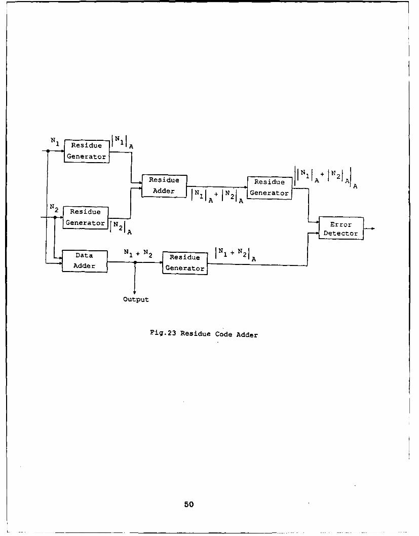
Residue lA
COutput
Fig.3 Ride Codedu AdderA I2 I
50

is always detected. First, let us consider only faults in the data adder causing its
output to be N1 + N 2 + ED. This error cannot be detected if and only if
IN, + N 2 + EDIA = IINI1A + IN21AA.
It can be easily shown that the above condition is equivalent to
JEDIA = 0.
An analogous result is obtained if the fault is in the residue generation following
the data adder.
If the fault is in the residue adder or in the corresponding residue generators,
then the input from this half of the circuit to the error detector is
IINIIA + IN21A + ERIA.
This error cannot be detected if and only if
IN1 + N21A = IINIIA + IN21A + ERIA.
It can be shown that this condition is equivalent to
I - ERIA = 0.
Let us now assume that a fault occurs either in the data adder part or in the
residue adder part of the circuit, but not in both. Furthermore, we are interested in
detecting faults that manifest as errors such that either W(ED) = 1 or W(-ER) =
1. The importance of detecting these errors is that for every ED (or ER) satisfying
W(ED) = 1 (or W(-ER) = 1) there always exists a single stuck-at fault that also
causes the same ED (or ER). Note that the set of faults that causes W(ED) = 1
or W(-ER) = 1 is circuit dependent.
51

The necessary and sufficient condition for these errors to be detected is A # 2j
where j E {0, 1, ... , n} where n is the number of bits in each addend. Residue
generation involves the division operation which is inherently more complex than
addition. Hence in designing a scheme to check addition we should choose a value
of A that causes the residue generation operation to be as simple as possible. As
suggested in [Rao, 1974], A should be of the form 2c - 1 where the integer c > 1. In
this case INIA is found by repeated addition of c bits of N with end-around carry.
Furthermore, Wakerly has described a scheme for designing a modulo 3 residue tree
without addition [Wake, 1978]. Implementation of an error- detecting scheme using
these residue generators requires approximately an overhead of 40% more than that
required by a duplication scheme when both schemes are implemented using two
input gates and the residue generators are non-trivial, i.e., A < 2,+2 -2. Moreover,
the duplication scheme detects all single stuck-at faults. Thus duplication is more
efficient than residue code scheme given in [Wake, 1978], both in terms of fault
coverage and gate count.
In conclusion, we remark that if A > 2,+2 - 2, where n is the number of bits
of each addend, the scheme given in Fig. 23 reduces to duplication.
Section 4.2. Error Correction Using Residue Codes
In this section we study the application of residue codes to the design of fault-
tolerant adders.
We first show that the class of residue codes discussed in the previous section
cannot be used for error correction. For purposes of error correction we define the
syndrome S as the difference (modulo A) between the inputs of the error detector
of Fig. 23. If the error is in the data adder part of the circuit, then
S= AN-+N2 +ED- INIA+IN2IA . =IEDIA"
52

If the error is in the residue adder part of the circuit, then
S = JN1 + NIj - JINIIA+INMIA +ER IA = I- ERIA.IA IA A-
Note that there are errors ED and ER such that W(ED) = W(-ER) = 1 and
IED! -I - 1, hence we cannot correct errors with binary arithmetic weight equal
to 1.
So we now introduce the concept of hi-residue codes, which is a generalization of
residue codes. The bi-residue code corresponding to any integer N is [N, INIA, INIBI
where A and B are positive integers. A possible scheme for an error-correcting adder
using bi-residue code is shown in Fig. 24. As in the previous section, the residue
generators are assumed to be implemented using the scheme in [Wake, 19781. In
this case, such a scheme for single-error correction requires an overhead of at least
100% more than that required by a Triple Modular Redundancy (TMR) scheme
when both are implemented using two input gates and the residue generators are
non-trivial, i.e., A, B < 2 ,+2 -2. Hence TMR is more efficient than bi-residue codes
in the design of single error correcting adders, both in terms of fault coverage and
gate count.
We end by re-emphasizing that the mapping between faults and error patterns
is circuit dependent and that if A, B > 2n+2 - 2, then the scheme shown in Fig. 24
reduces to TMR.
Section 4.3. Conclusion
In this section we studied the feasibility of using residue codes for the detection
and correction of errors in binary fixed point adders. The inherent complexity of
the residue generation operation substantially increases the area overhead. Our
study reveals that the design of single error detecting and correcting schemes using
residue codes fare poorly in comparison to duplication and TMR, respectively.
53

N2 Residue INA
Generator INA+N2
Ou pu Ge er to NN 1:++I I
N Ader IN Il A+IN IA eneator --Syndrome BAN 2 R sidue1 2 I Generator!
Ge er to Residue I NI+ NB2
Gennerator
N 1 R s i d u eO u t p u G e n r a to r I , + N 2 B+ S n r m]IOutputto NorcedOtu
Fi2 eorCdrecto sigBResidue Cds
A d e I N 1 G e e at5 4H N 1

Section 5. Conclusion
In this report two schemes have been proposed to detect errors caused by a
single short in a 32-bit bus. The first scheme is based on a modified form of the
Berger code. The check bits are generated from the 32 information bits by cascading
a number of ROMs. The second scheme considered for detecting a single short in
a 32-bit bus is to time-multiplex both the information bits and the test vectors on
the bus. If the bus is "flat," then the test vector basically consists of alternate O's
and l's. For an n-bit "non-flat" bus we need at least log 2 n] test vectors, and it is
therefore impractical to transmit these vectors in one clock cycle. Also, a scheme
for correcting a single-bit error and simultaneously detecting a double-bit error in
a 32-bit bus is proposed.
In this report we also studied several schemes for the design of self-checking
arithmetic circuits. We have concluded that all the self-checking adder schemes
studied require considerable area overhead. In particular, the MRB adder scheme
requires the maximum overhead because of the additional circuitry needed for en-
coding and decoding. MRB codes could provide an attractive technique for de-
signing self-checking systems if the encoding and decoding are done at the primary
inputs and outputs of the system, whereas all internal data is MRB coded. We
have also proposed a technique for designing a self-checking pipelined multiplier in
which only one of the multiplicands needs to be MRB coded.
Finally, we studied the feasibility of using residue codes for the detection and
correction of errors in binary fixed point adders. The inherent complexity of the
residue generation operation substantially increases the area overhead. Our study
reveals that the design of single error detecting and correcting schemes using residue
codes fare poorly in comparison to duplication and TMR, respectively.
55

Appendix I
LetA = (an-, an-29,.. ,ao) and
B = (b,-1, bn,_-,.., b0)
be the n-bit binary representation of two integers to be multiplied. Thus, the MRB
representation of A, denoted by M(A), is
M(A) = (an-1, a,- (D ae_2, an-2 ED an-3,..., al ED ao, ao).
Let 2'M(A) denote the j-bit left shift of M(A), i.e.,
2jM(A)- (an-,a- E ean-2,...,a, (Dao,ao,O,O,... ,O).
j zeros
It can be easily shown that 2jM(A) = M(2jA) where 2jA represents the j-bit left
shift of the number A.
In order to show that the block diagram of Fig. 22 computes the correct result
we must show that
bo 20M(A) +M b,2'M(A) +M''" +M b.-. 12"-M(A) = M(A * B),
where +M and * denote MRB addition and binary multiplication, respectively.
Using the fact that 2jM(A) = M(2jA), we may write
bo2 0M(A) +M b12'M(A) +M " " +M b,- 12-l M(A)
= M(bo20A) +M M(b,2 1 A) +M "". +M M(bn-. 12n- A)
= M(b020A + b121A +... + bn- 12n- 1 A)
= M(A * B)
56

References
[Berg, 1961] Berger, J. M. "A Note on Error Detecting Codes for Assym-
metric Channels." Information and Control, vol. 4, March
1961, pp. 68-73.
[Bose, 1985] Bose, Bella, and Der Jei Lin. "Systematic Unidirectional
Error Detecting Codes." IEEE Transactions on Computers,
Nov. 1985, pp. 1026-1032.
[Hart, 1987] Hartmann, C. R. P., and Parag K. Lala. "Fault Model De-
velopment for Fault Tolerant VLSI Design." Final Report
for RADC Contract No. F30602-81-C-0167, Task N-6-5788,
October 1987.
[Hsia, 1970] Hsiao, M. Y. "A Class of Optimal Minimum Odd-Weight-
Column SEC-DED Codes." I.B.M. Journal of Research and
Development, 1970, pp. 395-401.
[Lala, 1985] Lala, P. K. Fault Tolerant and Fault Testable Hardware De-
sign. Prentice Hall International, 1985.
[Luca, 19591 Lucal, H. M. "Arithmetic Operations for Digital Computers
Using Modified Reflected Binary Code." IRE Transactions
on Electronic Computers, Dec. 1959, pp. 449-458.
[Pete, 1972] Peterson, W. W., and E. J. Weldon, Jr. Error Correcting
Codes. 2nd ed. MIT Press, 1972.
[Prad, 1986] Fault Tolerant Computing- Theory and Techniques, Vol. I.
Ed. Pradhan, D. K. Prentice Hall, 1986.
[Rao, 1974] Rao, T. R. N. Error Coding for Arithmetic Processors. Aca-
demic Press, 1974.
57

[Wake, 1978] Wakerly, John. Error Detecting Codes, Self- Checking Cir-
cuits and Applications. North Holland, 1978.

MISSIONOf
Rome Air Development Center
RADC plans and executes research, development, test and selected
acquisition programs in support of Command, Control, Communications
and Intelligence (6l) activities. Technical and engineering support withinareas of competence is provided to ESD Program Offices (POs) and otherESD elements to perform effective acquisition of C3I systems. The areas
* of technical competence include communications, command and control,battle management, information processing, surveillance sensors,
* intelligence data collection and handling, solid state sciences,
electromagnetics, and propagation, and electronic, maintainability, and
* compatibility.
Related Documents