Louisiana Tech University Louisiana Tech Digital Commons Doctoral Dissertations Graduate School Summer 2004 Fabrication, characterization, and modeling of organic capacitors, Schoky diodes, and field effect transistors Mo Zhu Louisiana Tech University Follow this and additional works at: hps://digitalcommons.latech.edu/dissertations Part of the Electrical and Computer Engineering Commons , and the Materials Science and Engineering Commons is Dissertation is brought to you for free and open access by the Graduate School at Louisiana Tech Digital Commons. It has been accepted for inclusion in Doctoral Dissertations by an authorized administrator of Louisiana Tech Digital Commons. For more information, please contact [email protected]. Recommended Citation Zhu, Mo, "" (2004). Dissertation. 644. hps://digitalcommons.latech.edu/dissertations/644

Welcome message from author
This document is posted to help you gain knowledge. Please leave a comment to let me know what you think about it! Share it to your friends and learn new things together.
Transcript
Louisiana Tech UniversityLouisiana Tech Digital Commons
Doctoral Dissertations Graduate School
Summer 2004
Fabrication, characterization, and modeling oforganic capacitors, Schottky diodes, and field effecttransistorsMo ZhuLouisiana Tech University
Follow this and additional works at: https://digitalcommons.latech.edu/dissertations
Part of the Electrical and Computer Engineering Commons, and the Materials Science andEngineering Commons
This Dissertation is brought to you for free and open access by the Graduate School at Louisiana Tech Digital Commons. It has been accepted forinclusion in Doctoral Dissertations by an authorized administrator of Louisiana Tech Digital Commons. For more information, please [email protected].
Recommended CitationZhu, Mo, "" (2004). Dissertation. 644.https://digitalcommons.latech.edu/dissertations/644
NOTE TO USERS
Page(s) not included in the original manuscript and are
unavailable from the author or university. The manuscript
was scanned as received.
This reproduction is the best copy available.
UMI
Reproduced with permission of the copyright owner. Further reproduction prohibited without permission.

Reproduced with permission of the copyright owner. Further reproduction prohibited without permission.
FABRICATION, CHARACTERIZATION, AND MODELING OF
ORGANIC CAPACITORS, SCHOTTKY DIODES, AND FIELD
EFFECT TRANSISTORS
By
Mo Zhu, B. S.
A Dissertation Presented in Partial Fulfillment o f the Requirement for the Degree of
Doctor o f Philosophy in Engineering
COLLEGE OF ENGINEERING AND SCIENCE LOUISIANA TECH UNIVERSITY
August 2004
Reproduced with permission of the copyright owner. Further reproduction prohibited without permission.
UMI Number: 3134101
INFORMATION TO USERS
The quality of this reproduction is dependent upon the quality of the copy
submitted. Broken or indistinct print, colored or poor quality illustrations and
photographs, print bleed-through, substandard margins, and improper
alignment can adversely affect reproduction.
In the unlikely event that the author did not send a complete manuscript
and there are missing pages, these will be noted. Also, if unauthorized
copyright material had to be removed, a note will indicate the deletion.
UMIUMI Microform 3134101
Copyright 2004 by ProQuest Information and Learning Company.
All rights reserved. This microform edition is protected against
unauthorized copying under Title 17, United States Code.
ProQuest Information and Learning Company 300 North Zeeb Road
P.O. Box 1346 Ann Arbor, Ml 48106-1346
Reproduced with permission of the copyright owner. Further reproduction prohibited without permission.
LOUISIANA TECH UNIVERSITY
THE GRADUATE SCHOOL
07/26/2004Date
We hereby recommend that the dissertation prepared imder our supervision
by Mo Zhu__________________________________________________________________
entitled Fabrication. Characterization, and Modeling of Organic Capacitors. Schottky Diodes,
and Field Effect Transistors
be accepted in partial fulfillment of the requirenierits-
Ph. D. in Enaineerina
—fbr ^ 1*. Degiee of
Recomn^ndation concurred in:
'- * U — ______
Director of Graduate Studies
Dean of the College
Advisory Committee
A p p ^ d :
ervisor of Dissertation Research
Head of Department
Department
Annroved:
Dean of the Graduate School
GS Form 13(5/03)
Reproduced with permission of the copyright owner. Further reproduction prohibited without permission.
APPROVAL FOR SCHOLARLY DISSEMINATION
The author grants to the Prescott Memorial Library of Louisiana Tech University the right to
reproduce, by appropriate methods, upon request, any or all portions of this Dissertation. It is understood
that “proper request” consists o f the agreement, on the part of the requesting party, that said reproduction
is for his personal use and that subsequent reproduction will not occur without written approval o f the
author o f this Dissertation. Further, any portions o f the Dissertation used in books, papers, and other
works must be appropriately referenced to this Dissertation.
Finally, the author of this Dissertation reserves the right to publish freely, in the literature, at
any time, any or all portions of this Dissertation.
Author
P, , > / / ■20 Q HDate *
GS Form 14 (5/03)
Reproduced with permission of the copyright owner. Further reproduction prohibited without permission.
ABSTRACT
The objectives of this project are to fabricate, characterize, and model organic
microelectronic devices by traditional lithography techniques and Technology Computer
Aided Design (TCAD).
Organic microelectronics is becoming a promising field due to its number of
advantages in low-cost fabrication for large area substrates. There have been growing
studies in organic electronics and optoelectronics. In this project, several organic
microelectronic devices are studied with the aid of experimentation and numerical
modeling.
Organic metal-insulator-metal (MIM) and metal-insulator-semiconductor (MIS)
capacitors consisting o f insulating polymer poly(4-vinylphenol) (PVP) have been
fabricated by spin-coating, photo lithography, and reactive ion etching techniques. Based
on the fabricated devices, the dielectric constant o f the (PVP) is calculated to be about 5.6
- 5.94. The MIS capacitor consisting o f organic semiconductor pentacene has been
investigated. The hole concentration o f pentacene is determined to be around 8x10*^ cm'^.
Schottky diodes consisting o f aluminum and a layer o f p-type semiconducting
polymer poly[2-methoxy-5-(2’-ethyl-hexyloxy)-l,4-phenylene vinylene] (MEH-PPV)
have been fabricated. Based on the current-voltage (I-V) and capacitance-voltage (C-V)
measurements, the temperature dependence o f hole mobility in MEH-PPV has been
extracted by the space-charge limited conduction (SCLC) model, from 300 to 400 K.
Ill
Reproduced with permission of the copyright owner. Further reproduction prohibited without permission.
IV
Moreover, the value of the effective hole density for MEH-PPV has been determined to
1 7 - 3be 2.24x10 cm' . Numerical simulations have been carried out to identify the
parameters which affect the performance o f devices significantly.
Organic n- and p-channel field-effect transistors (FETs) have been designed and
fabricated. By using Naphthalene-tetracarboxylic-dianhydride (NTCDA) as an organic
semiconductor, n-chaimel FETs have been fabricated and characterized. At room
temperature, the device characteristics have displayed electron mobility o f 0.016 cm^A^s,
threshold voltage o f -32 V, and on/off ratio o f 2.25 x 1 0 . Pentacene, an organic
semiconductor offering high device performance, has been employed to fabricate the p-
channel FETs. At room temperature, the device characteristics have displayed hole
mobility o f 0.26 cm /Vs, threshold voltage o f -3.5 V, subthreshold slope o f 2.5 V/decade,
and on/off ratio o f 10 . The temperature and field dependence o f mobility has been
studied based on the experimental results. Based on numerical simulations, the influence
o f bulk traps has also been identified, and the field-dependent mobility model has been
used to obtain more accurate simulation results. Furthermore, electrostatically assembled
monolayer (poly(dimethyldiallylammonium chloride) (PDDA)) is introduced at the
organic/insulator interface to improve the performance o f the FETs.
The efforts carried out in this work appear to be the first reported attempt at the
investigation o f the temperature dependence o f mobility for the given organic devices,
and the surface modification of organic FETs by electrostatically assembled monolayer.
Reproduced with permission of the copyright owner. Further reproduction prohibited without permission.
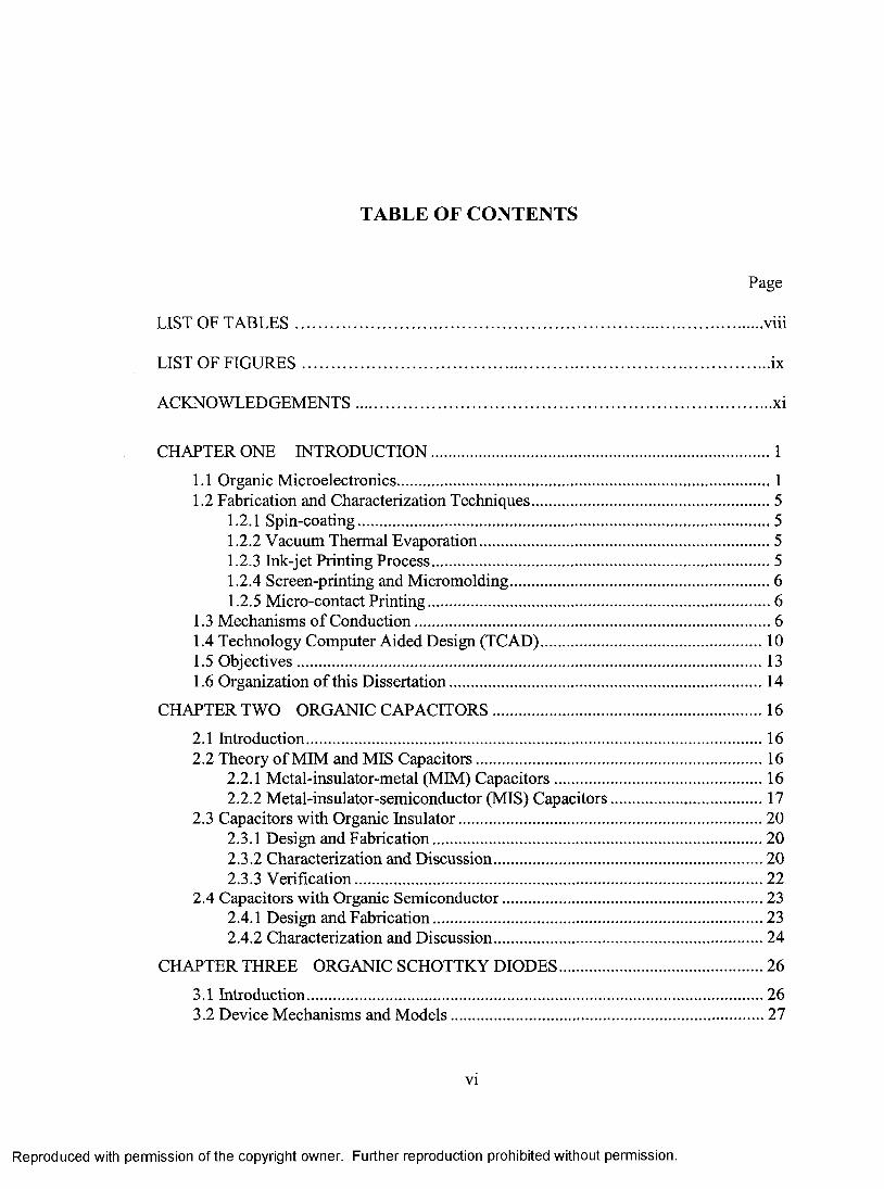
TABLE OF CONTENTS
Page
LIST OF TA B LES..................................................................................................................... viii
LIST OF FIG U R ES..................................................................................................................... ix
ACKNOWLEDGEMENTS........................................................................................................ xi
CHAPTER ONE INTRODUCTION...................................................................................... 1
1.1 Organic Microelectronics...............................................................................................11.2 Fabrication and Characterization Techniques.............................................................5
1.2.1 Spin-coating........................................................................................................ 51.2.2 Vacuum Thermal Evaporation..........................................................................51.2.3 Ink-jet Printing Process......................................................................................51.2.4 Screen-printing and Micromolding.................................................................. 6
1.2.5 Micro-contact Printing.......................................................................................6
1.3 Mechanisms o f Conduction.......................................................................................... 6
1.4 Technology Computer Aided Design (TCAD)........................................................ 101.5 Objectives......................................................................................................................131.6 Organization o f this Dissertation............................................................................... 14
CHAPTER TWO ORGANIC CAPACITORS.....................................................................16
2.1 Introduction....................................................................................................................162.2 Theory o f MIM and MIS Capacitors.........................................................................16
2.2.1 Metal-insulator-metal (MIM) Capacitors..................................................... 162.2.2 Metal-insulator-semiconductor (MIS) Capacitors....................................... 17
2.3 Capacitors with Organic Insulator............................................................................. 202.3.1 Design and Fabrication....................................................................................202.3.2 Characterization and Discussion.................................................................... 202.3.3 Verification....................................................................................................... 22
2.4 Capacitors with Organic Semiconductor.................................................................. 232.4.1 Design and Fabrication....................................................................................232.4.2 Characterization and Discussion.................................................................... 24
CHAPTER THREE ORGANIC SCHOTTKY DIODES....................................................26
3.1 Introduction................................................................................................................... 263.2 Device Mechanisms and M odels............................................................................... 27
VI
Reproduced with permission of the copyright owner. Further reproduction prohibited without permission.
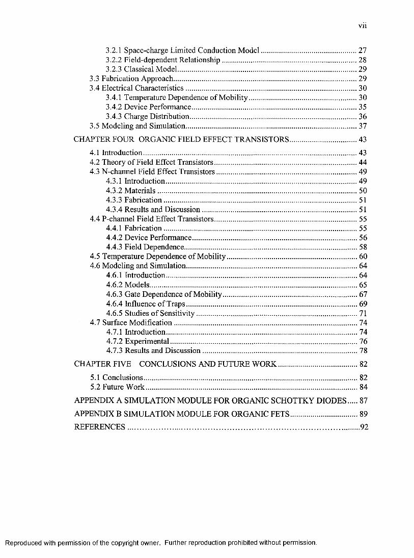
Vll
3.2.1 Space-charge Limited Conduction M odel....................................................273.2.2 Field-dependent Relationship.........................................................................283.2.3 Classical Model.................................................................................................29
3.3 Fabrication Approach...................................................................................................293.4 Electrical Characteristics............................................................................................ 30
3.4.1 Temperature Dependence o f M obility...........................................................303.4.2 Device Performance......................................................................................... 353.4.3 Charge Distribution.......................................................................................... 36
3.5 Modeling and Simulation............................................................................................ 37
CHAPTER FOUR ORGANIC FIELD EFFECT TRANSISTORS.....................................43
4.1 Introduction................................................................................................................... 434.2 Theory o f Field Effect Transistors.............................................................................444.3 N-channel Field Effect Transistors............................................................................49
4.3.1 Introduction....................................................................................................... 494.3.2 M aterials............................................................................................................504.3.3 Fabrication........................................................................................................ 514.3.4 Results and Discussion....................................................................................51
4.4 P-channel Field Effect Transistors............................................................................. 554.4.1 Fabrication........................................................................................................ 554.4.2 Device Performance......................................................................................... 564.4.3 Field Dependence............................................................................................. 58
4.5 Temperature Dependence of M obility.......................................................................604.6 Modeling and Simulation............................................................................................ 64
4.6.1 Introduction....................................................................................................... 644.6.2 Models................................................................................................................ 654.6.3 Gate Dependence o f Mobility.........................................................................674.6.4 Influence o f Traps............................................................................................ 694.6.5 Studies o f Sensitivity.......................................................................................71
4.7 Surface M odification...................................................................................................744.7.1 Introduction....................................................................................................... 744.7.2 Experimental..................................................................................................... 764.7.3 Results and Discussion....................................................................................78
CHAPTER FIVE CONCLUSIONS AND FUTURE W ORK........................................... 82
5.1 Conclusions................................................................................................................... 825.2 Future W ork.................................................................................................................. 84
APPENDIX A SIMULATION MODULE FOR ORGANIC SCHOTTKY DIODES 87
APPENDIX B SIMULATION MODULE FOR ORGANIC FETS.....................................89
REFERENCES............................................................................................................................ 92
Reproduced with permission of the copyright owner. Further reproduction prohibited without permission.
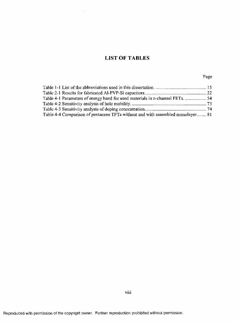
LIST OF TABLES
Page
Table 1-1 List o f the abbreviations used in this dissertation..................................................15Table 2-1 Results for fabricated Al-PVP-Si capacitors..........................................................22Table 4-1 Parameters o f energy band for used materials in n-channel FETs......................54Table 4-2 Sensitivity analysis o f hole mobility....................................................................... 73Table 4-3 Sensitivity analysis o f doping concentration..........................................................74Table 4-4 Comparison of pentacene TFTs without and with assembled monolayer 81
Vlll
Reproduced with permission of the copyright owner. Further reproduction prohibited without permission.
LIST OF FIGURES
Page
Figure Figure Figure Figure Figure Figure Figure Figure Figure Figure Figure Figure 2 Figure 2 Figure 2 Figure 2 Figure 2 Figure 2 Figure 2 Figure 2 Figure 2 Figure 2 Figure 3 Figure 3 Figure 3 Figure 3 Figure 3 Figure 3 Figure 3 Figure 3 Figure 3 Figure 3 Figure 3 Figure 3 Figure 3 Figure 3 Figure 3
-1 Overview of applications o f conducting polymers in microelectronics [2]....... 2-2 Schematic structures o f TFTs realized by organic materials [1]......................... 3-3 Schematic structures LEDs realized by organic materials [1]..............................3-4 Comparisons o f typical organic and inorganic semiconductors [1].................... 4■5 Performance of organic and hybrid semiconductors [1]....................................... 4- 6 Radical cation (polaron) formation and migration [23].........................................8-7 Creation and transportation o f a soliton [23].......................................................... 8
-8 Intersoliton hopping and interaction o f solitons [23].............................................9-9 Classic TCAD domains and samples o f information [26].................................. 11-10 Schematic time-line o f TCAD R&D for device analysis [26]........................11-11 TCAD applications in “MegaFab” and “Fabless” environments [26]............13-1 Molecular structure o f poly(4-vinylphenol) (PVP).............................................. 17-2 Schematic structure o f MIS capacitor....................................................................18-3 Energy band diagram of the MIS capacitor at thermal equilibrium.................. 19-4 A fabricated MIM capacitor: (a) schematic structure and (b) micrograph 21-5 C-V characteristics o f MIM capacitors with PVP at low frequency.................21- 6 Capacitance-voltage characteristics o f Al-PVP-Si capacitors at 100 kHz 22-7 Schematic structure o f MIS capacitors with organic semiconductor................24- 8 Molecular structure o f pentacene........................................................................... 24-9 Energy band o f pentacene MIS capacitors............................................................25-10 C-V characteristics o f metal-PVP-pentacene stmcture at high frequency.... 25-1 Molecular structure o f MEH-PPV......................................................................... 27-2 Fabrication steps o f the MEH-PPV based Schottky diodes................................30-3 Energy-band alignment o f the ITO/MEH-PPV/Al structures............................ 31-4 J-V characteristics o f ITO/MEH-PPV/Al Schottky diodes with temperature. 32-5 J-V^ characteristics o f ITO/MEH-PPV/Al diodes at V i t o /a i > 0 V ................... 32- 6 Extracted hole mobility in MEH-PPV as a function o f temperature.................33-7 Temperature dependence key parameters o f Schottky diodes........................... 34- 8 J-V characteristics o f ITO/MEH-PPV/Al diodes at 325 K .................................35-9 J-V characteristics o f ITO/MEH-PPV/Al diodes with film thickness.............. 36-10 C-V Characteristics o f ITO/MEH-PPV/Al diodes at high frequency.............37-11 I-V behavior o f MEH-PPV Schottky diodes with hole injection.................... 38-12 I-V behavior o f MEH-PPV Schottky diodes with bulk traps...........................39-13 Comparison o f experimental and simulation results with forward bias......... 41-14 Hole density from cathode to anode with different forward bias.................... 42-15 Electric field from cathode to anode with different forward bias....................42
IX
Reproduced with permission of the copyright owner. Further reproduction prohibited without permission.
X
Figure 4-1 Organic FETs configuration: a) Top-contact; b) Bottom-contact [90].............45Figure 4-2 Band diagram of an ideal MIS structures at equilibrium.................................... 45Figure 4-3 MIS structures under (a) accumulation, (b) depletion, and (c) inversion.........46Figure 4-4 Molecular structures o f NTCDA (left) and PPy (right).......................................50Figure 4-5 Structure o f the n-channel FETs............................................................................. 50Figure 4-6 Output characteristics o f the NTCDA FETs.........................................................52Figure 4-7 Transfer characteristics o f the NTCDA FETs at Vds = 20 V ..............................54Figure 4-8 Transfer characteristics o f the NTCDA FETs at Vds = 60 V ..............................54Figure 4-9 Schematic structure o f fabricated pentacene TFTs.............................................. 55Figure 4-10 Output (a) and transfer characteristics (b) o f pentacene TFTs.........................56Figure 4-11 Output (a) and transfer characteristics (b) o f pentacene TFTs.........................57Figure 4-12 Gate voltage dependent mobility in pentacene TFTs at room temperature.. 59Figure 4-13 Temperature dependent mobility at Yds = -20 V and Yds = -5 Y .....................61Figure 4-14 Temperature dependent mobility at Yds = -30 Y and Yds = -5 Y .....................62Figure 4-15 Temperature dependence o f key parameters...................................................... 63Figure 4-16 Gate voltage dependence o f mobility in pentacene FETs................................ 67Figure 4-17 Simulation o f output characteristics with gate dependence..............................6 8
Figure 4-18 Simulation output characteristics o f gate dependence and bulk traps 6 8
Figure 4-19 Simulation o f transfer characteristics with bulk traps.......................................69Figure 4-20 Influence o f trap density to transfer characteristics o f FETs............................70Figure 4-21 Distribution o f electric field along the center o f simulated FETs................... 71Figure 4-22 Distribution o f hole current along the center o f simulated FETs.................... 71Figure 4-23 Transfer and output characteristics with change o f hole mobility.................. 72Figure 4-24 Transfer and output characteristics with change o f doping concentration.... 73Figure 4-25 LBL assembly by alternate adsorption o f polyions [120]................................ 75Figure 4-26 SEM for pentacene TFTs (a) without and (b) with assembled monolayer... 77 Figure 4-27 Transfer characteristics o f TFTs without and with assembled m onolayer... 78 Figure 4-28 Output characteristics o f TFTs without and with assembled monolayer 80
Reproduced with permission of the copyright owner. Further reproduction prohibited without permission.
ACKNOWLEDGEMENTS
I would like to express my lasting gratitude and appreciation to my advisor. Dr.
Kody Varahramyan, and my former co-advisor. Dr. Tianhong Cui, who have guided and
instructed me in the scientific method and honest attitude. Their invaluable advice,
continuous guidance, encouragement, and assistance have been necessary for the
completion o f this dissertation. Special acknowledgements are extended to Dr. Yi Su, Dr.
Debasish Kuila, Dr. Cheng Luo, and Dr. Alfred Gunasekaran, for their advice and serving
as advisory committee members o f this dissertation.
The author would like to thank the staff at Institute for Micromanufacturing for
their help and support with the experimental and simulation parts o f this work. Much
gratitude is extended to Mr. Abdul Khaliq, Mr. Dee Tatum, Dr. Guirong Liang, and Ms.
Jingshi Shi for their valuable discussion, support, and contributions.
My deepest appreciation goes to my parents and my wife. I could not have been
what I am today without them. Their love and encouragement accompanied me through
this research.
XI
Reproduced with permission of the copyright owner. Further reproduction prohibited without permission.
CHAPTER ONE
INTRODUCTION
1.1 Organic Microelectronics
Organic microelectronics is becoming a promising field due to its number o f
advantages in low-cost fabrications for large-area substrates. There have been growing
studies in organic microelectronics to improve semiconducting, conducting, and light-
emitting properties o f organics (polymers, oligomers) and hybrids (organic-inorganic
composites) through novel synthesis and process techniques. Performance improvements,
coupled with the ability to process these active materials at relatively low temperatures
over large areas on glass or paper by the ink-jet printing technique, will provide unique
technologies, generate new applications, and form factors to address the growing needs
for pervasive computing and enhanced connectivity [1 ].
Conducting polymers have potential applications at almost all levels of
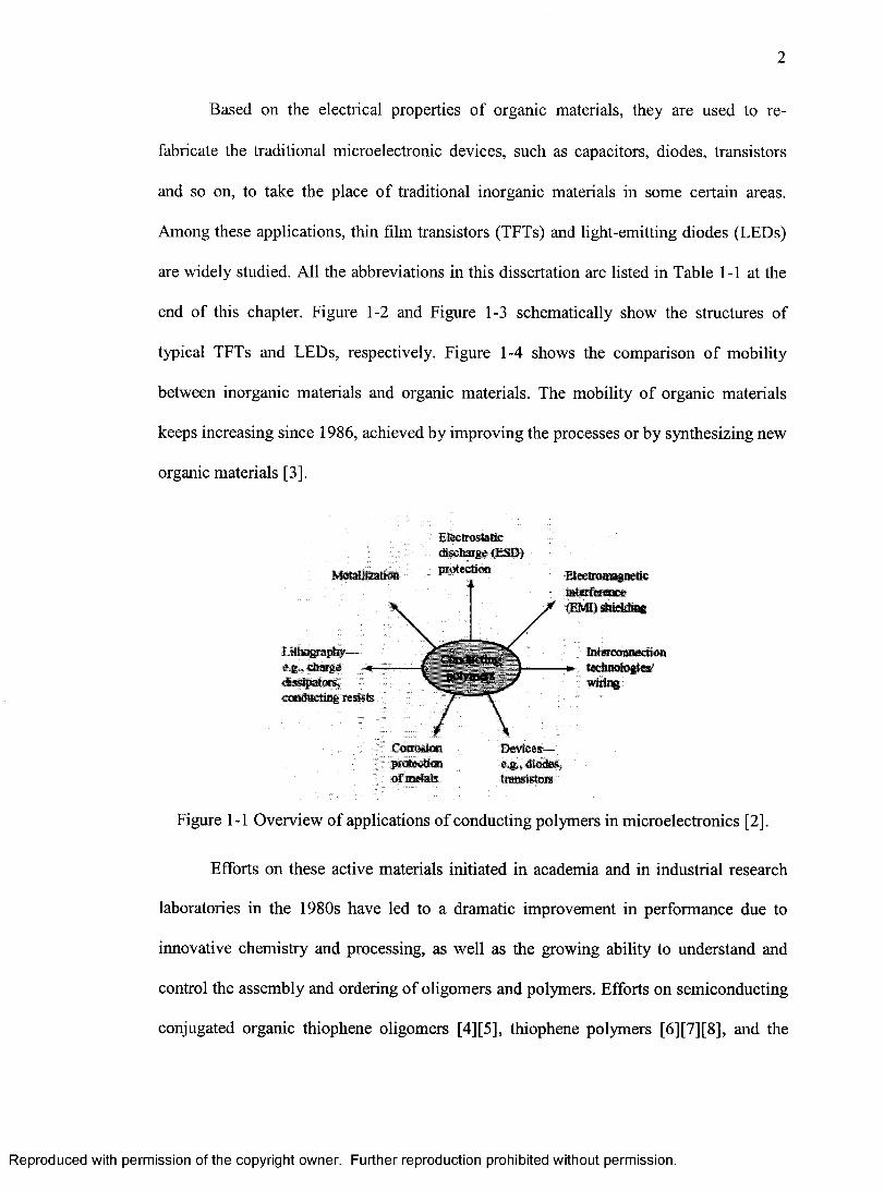
microelectronics [2] as shown in Figure 1-1. Conducting polymers have applications in
the areas o f lithography, metallization, corrosion-protecting coatings for metals, and
electrostatic discharge, protective coatings for packages, and housings o f electronic
equipment. Moreover, two important areas o f applications for conducting polymers in the
future are their possible use in interconnection technology and as novel organic materials
in microelectronic devices.
Reproduced with permission of the copyright owner. Further reproduction prohibited without permission.
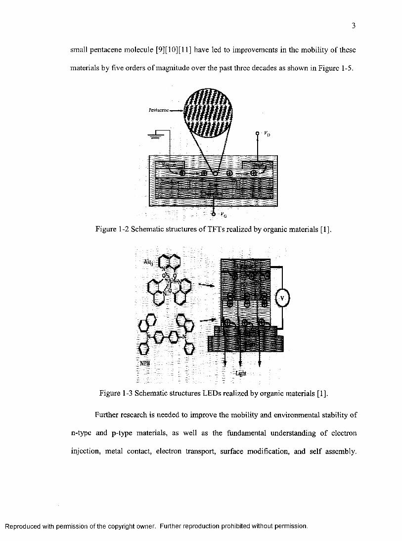
Based on the electrical properties o f organic materials, they are used to re-
fahricate the traditional mieroeleetronic devices, such as capacitors, diodes, transistors
and so on, to take the place of traditional inorganic materials in some certain areas.
Among these applications, thin film transistors (TFTs) and light-emitting diodes (LEDs)
are widely studied. All the abhreviations in this dissertation are listed in Table 1-1 at the
end o f this chapter. Figure 1-2 and Figure 1-3 schematically show the structures of
typical TFTs and LEDs, respectively. Figure 1-4 shows the comparison o f mobility
between inorganic materials and organic materials. The mobility o f organic materials
keeps increasing since 1986, achieved by improving the processes or by synthesizing new
organic materials [3].
NfelaiUzation
Electrostatie dtscli&rgie (E5D) protection
Litiwgraphy— e.g., charge dtssipatofs,condttctii^ resists
C.cnducttngpol>'mers
Electrcwr^^u ^ erfe ren ce(EMI)shMdiitg
iMercouKcticutechnolopes/wiring
Corrosion protection o f metals
Devices— e.g., diodes, transistoTS
Figure 1-1 Overview of applications o f conducting polymers in microelectronics [2].
Efforts on these active materials initiated in academia and in industrial research
laboratories in the 1980s have led to a dramatic improvement in performance due to
innovative chemistry and processing, as well as the growing ability to understand and
control the assembly and ordering o f oligomers and polymers. Efforts on semiconducting
conjugated organic thiophene oligomers [4][5], thiophene polymers [6][7][8], and the
Reproduced with permission of the copyright owner. Further reproduction prohibited without permission.
small pentacene molecule [9][10][11] have led to improvements in the mobility o f these
materials by five orders o f magnitude over the past three decades as shown in Figure 1-5.
Pentacenic 1-■ r,
Source
Insulator
Figure 1-2 Schematic structures o f TFTs realized by organic materials [1].
-■’t ■ ■.
NPB
1 = T1 - u
Light
Figure 1-3 Schematic structures LEDs realized by organic materials [1].
Further research is needed to improve the mobility and environmental stability o f
n-type and p-type materials, as well as the fundamental understanding o f electron
injection, metal contact, electron transport, surface modification, and self assembly.
Reproduced with permission of the copyright owner. Further reproduction prohibited without permission.
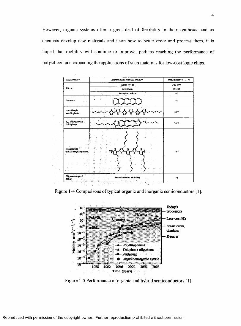
However, organic systems offer a great deal o f flexibility in their synthesis, and as
chemists develop new materials and learn how to better order and process them, it is
hoped that mobility will continue to improve, perhaps reaching the performance of
polysilicon and expanding the applications o f such materials for low-cost logic chips.
MsMtty- (aa^ V s “ ’ ;i
3C1&~W50-i€0
siiirai
C C C C O-1
10-'
dithJopbeiM 10-'
Reg;ioi«p][ar poly( ) 10” '
hybnA Fb«oetiiytainuh»-<kt iodid« -I
Figure 1-4 Comparisons o f typical organic and inorganic semiconductors [1].
Ibdas^Si waiera
ilvbndsPo v-S Organics
a-Si;H
10"
Pc4) ( i3ijenes Thiophene oligomm
■ Pisi aceffle# Orgamolitoigaiiic hyhiid
' > I Ii>iS8 1992 1996 2000 2004 2008
Time (years)
Figure 1-5 Performance o f organic and hybrid semiconductors [1].
Reproduced with permission of the copyright owner. Further reproduction prohibited without permission.
1.2 Fabrication and Characterization Techniques
Organic materials including polymers and oligomers can be deposited onto a
substrate using various techniques like spin-coating, thermal evaporation, photochemical
lithography, ink-jet printing process, screen-printing, micromolding, micro-contact
printing (pCP) [12], etc.
1.2.1 Spin-coating
Spin coating is generally regarded as the best way to deposit a uniform coating for
many applications such as photoresist coating and insulating layer coating. It gives
optimal coverage with minimum material usage. This deposition technique is extremely
desirable because the process is simple, safe, and inexpensive. A detailed description o f
spin-coating technique is demonstrated in literature [13].
1.2.2 Vacuum Thermal Evaporation
The vacuum thermal evaporation technique consists o f heating until evaporation
o f the material is to be deposited. The material vapor finally condenses in the form o f a
thin film on the substrate surface and on the vacuum chamber walls. Usually, low
pressures about 10'^ or 10'^ Torr are used, to avoid the reaction between the vapor and
atmosphere. Small molecular organics can be deposited by thermal vacuum evaporation
such as NTCDA and pentacene [14] [15].
1.2.3 Ink-iet Printing Process
Ink-jet printing process is a method in which the polymer solution takes the place
o f the toner in a printer. In this method, the polymer pattern can be directly printed onto
the substrate. With this technique, the polymer solution can be applied to the substrate in
the size o f a pixel, giving very high-resolution patterns and the ability to separate pixels
Reproduced with permission of the copyright owner. Further reproduction prohibited without permission.
of red, green, and blue emitting polymers onto the substrate. Ink-jet printing has been
applied to polyvinylcarbazole (PVK)/dye composites using a commercial inkjet printer
with 65 pm nozzles [16]. Ink-jet printing has also been used to deposit the conducting
polymer to create dual-color light-emitting pixels [17].
1.2.4 Screen-printing and Micromolding
Screen-printing and micromolding are recently used to fabricate functional all
polymer transistors [5][18] with advantages o f mass production and transferability.
Screen-printing prints patterns by squeezing ink through a predefined screen mask and
transferring patterns to the substrate. Micromolding is one type o f soft lithography
technique to pattern source and drain electrodes.
1.2.5 Micro-contact Printing
The micro-contact printing technique is based on the selective transfer o f polymer
material to a substrate via a polydimethylsiloxane (PDMS) stamp to obtain desired
patterns or exposed and covered regions o f the substrate. This can be used for the
deposition o f polymer materials by area-selected electropolymerization [19] or area-
selected deposition [2 0 ].
1.3 Mechanisms of Conduction
Organic solids are formed by covalent bonds without electron overlap. There are
no significant hole and electron carriers in the traditional sense. The excitations exist on
organic molecules in the states o f solitons, polarons, and bipolarons [21]. Organic
chemistry shows that conjugated double bonds behave quite differently from isolated
double bonds. As indicated, conjugated double bonds act collectively, knowing that the
next nearest bond is also double [1][2]. Hiickel’s theory [22] and other simple theories
Reproduced with permission of the copyright owner. Further reproduction prohibited without permission.
7
predict that tt electrons are delocalized over the entire chain and that the band gap
becomes vanishingly small for a long enough chain. One reason for this prediction is the
character o f a 7r molecular orbital, including the p orbitals o f all carbon atoms along the
chain o f conjugated double bonds. When looking at the distribution o f electron density, to
which all filled molecular orbitals contribute, the electrons are predicted to be blocked off
rather evenly along the entire chain [23]. In other words, all bonds are predicted to be
equal. One reason why polyacetylene is a semiconductor and not a conductor is because
the bonds are not equal. There is a distinct alternation; every second bond having some
double-bond character.
The role o f the dopant is either to remove or to add electrons to the polymer. For
example, iodine (I2) will abstract an electron under formation of an 13 ion. If an electron
is removed from the top o f the valence band o f a semiconductive polymer, such as
polyacetylene or polypyrrole, the vacancy (hole) created does not delocalize completely,
as would be predicted from classical band theory. If an electron is removed from one
carbon atom, a radical cation will be produced.
The radical cation or anion (polaron) is localized, partly because o f Coulomb
attraction to its counterion (Is“), which is the quasiparticle composed of a single
electronic charge dressed with a local geometrical relaxation o f the bond lengths [21]. A
polaron can be thought o f as a bound state o f a charged soliton and a neutral soliton
whose midgap energy states hybridize to form bonding and antibonding levels. A polaron
has normally a very low mobility, partly because o f a local change in the equilibrium
geometry o f the radical cation relative to the neutral molecule [24].
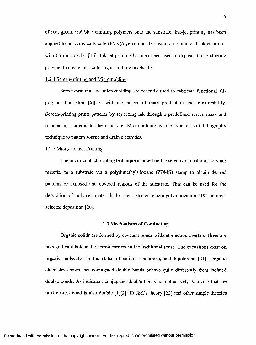
Reproduced with permission of the copyright owner. Further reproduction prohibited without permission.
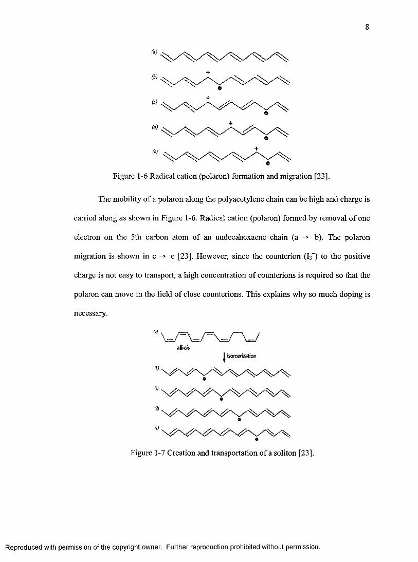
Figure 1-6 Radical cation (polaron) formation and migration [23].
The mobility o f a polaron along the polyacetylene chain can be high and charge is
carried along as shown in Figure 1-6. Radical cation (polaron) formed by removal o f one
electron on the 5th carbon atom of an undecahexaene chain (a b). The polaron
migration is shown in c e [23]. However, since the counterion (la”) to the positive
charge is not easy to transport, a high concentration o f counterions is required so that the
polaron can move in the field o f close counterions. This explains why so much doping is
necessary.
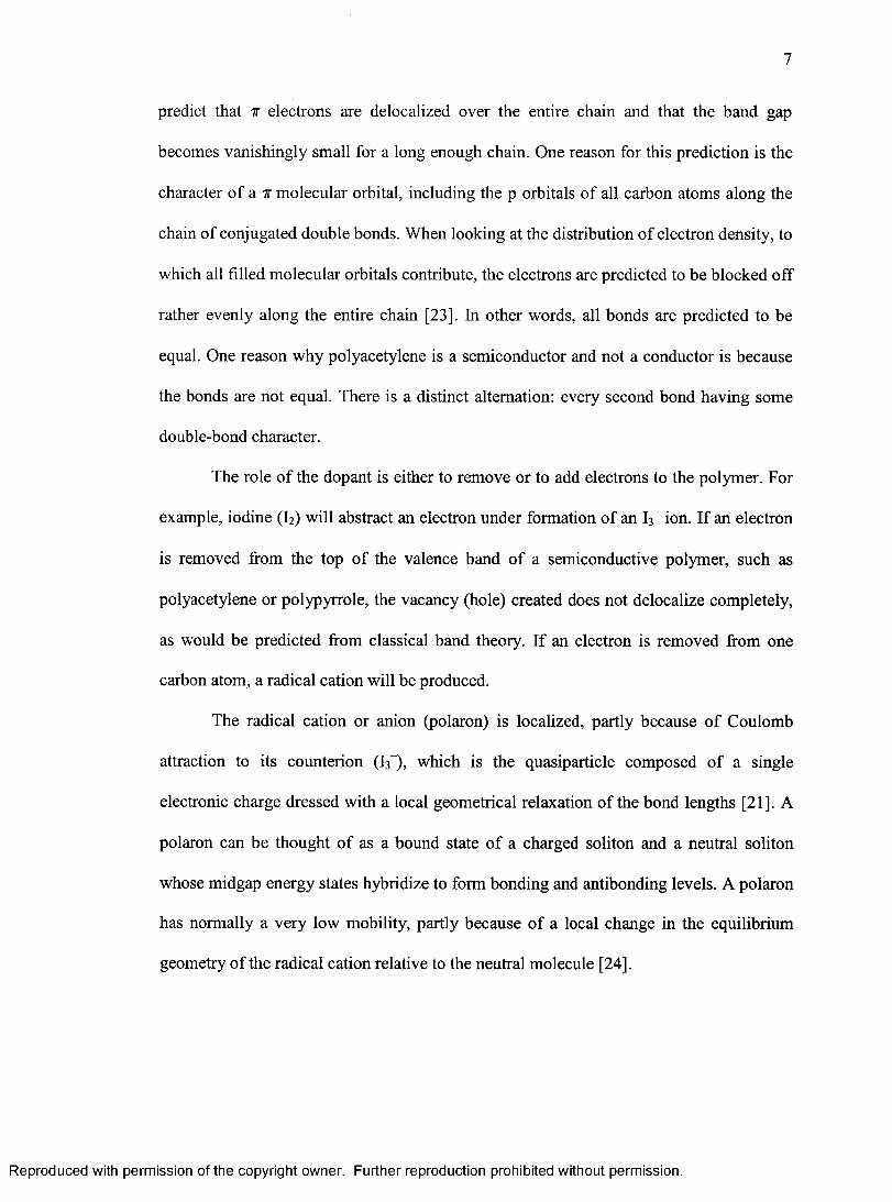
alt-ds
i 'isomerization
(ij
Figure 1-7 Creation and transportation o f a soliton [23].
Reproduced with permission of the copyright owner. Further reproduction prohibited without permission.
If a second electron is removed from an already-oxidized section o f the polymer,
either a second independent polaron may be created or a bipolaron (a bound state o f two
charged solitons o f like charge, or two polarons whose neutral solitons annihilate each
other with two corresponding midgap levels [2 1 ]) is formed if it is the unpaired electron
of the first polaron that is removed [21][23]. The two positive charges o f the bipolaron
are not independent, but move as a pair, like the Cooper pair in the theory of
superconductivity. While a polaron, being a radical cation, has a spin o f 1/2, the spins o f
the bipolaron’s sum is S = 0. Other carriers in polymer chain defects which are important
for conductivity in polyacetylene are solitary wave defects solitons. Figure 1-7 shows
how a cis-polyacetylene chain by undergoing thermal isomerization to trans-structure
may create a defect, a stable free radical: this is a neutral soliton which, although it can
propagate along the chain, may not carry any charge itself. A soliton is created by
isomerisation o f cis-polyacetylene (a ^ b) and moves by pairing with an adjacent
electron (b e) [23]. On the other hand, it may contribute to the charge transfer between
different chains.
Bulk conductivity in the polymer material is limited by the need for the electrons
to jump from one chain to the next. For example, in molecular terms an intermolecular
charge transfers reaction. It is also limited by macroscopic factors such as bad contacts
between different crystalline domains and grain boundaries in the material.
V VFigure 1-8 Intersoliton hopping and interaction o f solitons [23].
Reproduced with permission of the copyright owner. Further reproduction prohibited without permission.
10
One mechanism proposed to account for conductivity by charge-hopping between
different polymer chains is “intersoliton hopping” (Figure 1-8). In intersoliton hopping,
charged solitons (bottom in Figure 1 -8 ) are trapped by dopant counterions, while neutral
solitons (top) are free to move. A neutral soliton on a chain close to one with a charged
soliton can interact: the electron hops from one defect to the other [23]. Here, an electron
is jumping between localized states on adjacent polymer chains; the role o f the soliton is
to move around and to exchange an electron with a closely located charged soliton, which
is localized. The mechanism at work in intersoliton hopping is very similar to that
operating in most conducting polymers somewhere in between the metallic state at high
doping and the semiconducting state at very low doping. All conjugated polymers do not
carry solitons, but polarons can be found in most o f them. Charge transport in polaron-
doped polymers occurs via electron transfer between localized states being formed by
charge injection on the chain [25].
1.4 Technology Computer Aided Design (TCAD)
TCAD modeling is the art and science of abstracting a device and electrical
behavior o f integrated circuit (IC) and supported by critical analysis including detailed
understanding based on computer simulations. Specifically, a TCAD tool set has emerged
over the last two decades— along with a methodology for its use—that takes input from
the IC mask information and specifications o f the processing technology and
systematically supports development o f electrical representations using these
“computational prototypes.” TCAD models can capture both higher level behaviors as
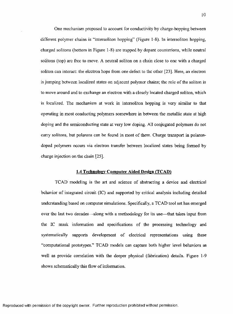
well as provide correlation with the deeper physical (fabrication) details. Figure 1-9
shows schematically this flow o f information.
Reproduced with permission of the copyright owner. Further reproduction prohibited without permission.
11
Technology Computer-Aided Design
MuiicsJSSk-
lnti:ri;;KiiieLts
o
Circuit
Process
_ A _ T'TciiiBURigy I’jks
De-fflis SBslfit
Figure 1-9 Classic TCAD domains and samples o f information [26].
The tools that define the TCAD field including process, device and circuit
modeling have evolved steadily over the past two decades, moving from research
prototypes (both in industry and academia) towards robust workhorse engines that
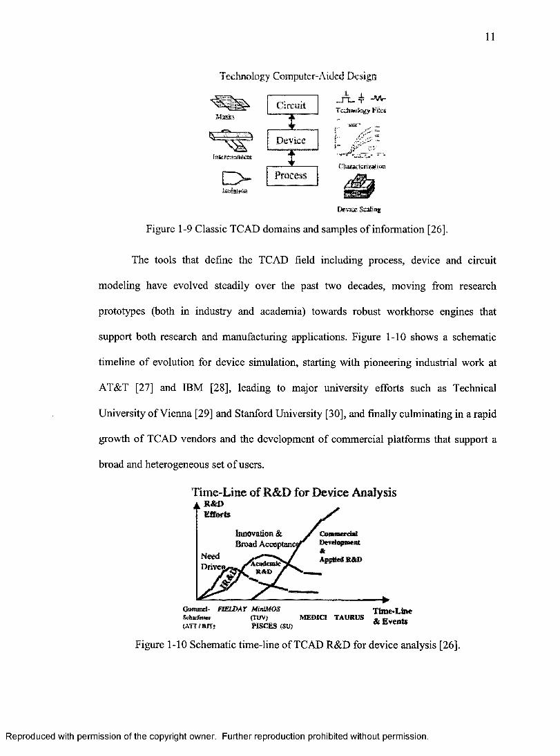
support both research and manufacturing applications. Figure 1-10 shows a schematic
timeline o f evolution for device simulation, starting with pioneering industrial work at
AT&T [27] and IBM [28], leading to major university efforts such as Technical
University o f Vienna [29] and Stanford University [30], and finally culminating in a rapid
growth o f TCAD vendors and the development o f commercial platforms that support a
broad and heterogeneous set o f users.
Time-Line of R&D for Device Analysis A m m
InrwivattoB & Broiid
NeedDrive
OwaaeJ- mLMT MmiMOS T lm e-LiiieScliWfiMW <TUV> MEBICI TAURUS . „ ,(A T T /ilT ) n S C B IC S U ) « B V e i l |5
Figure 1-10 Schematic time-line o f TCAD R&D for device analysis [26].
Reproduced with permission of the copyright owner. Further reproduction prohibited without permission.
12
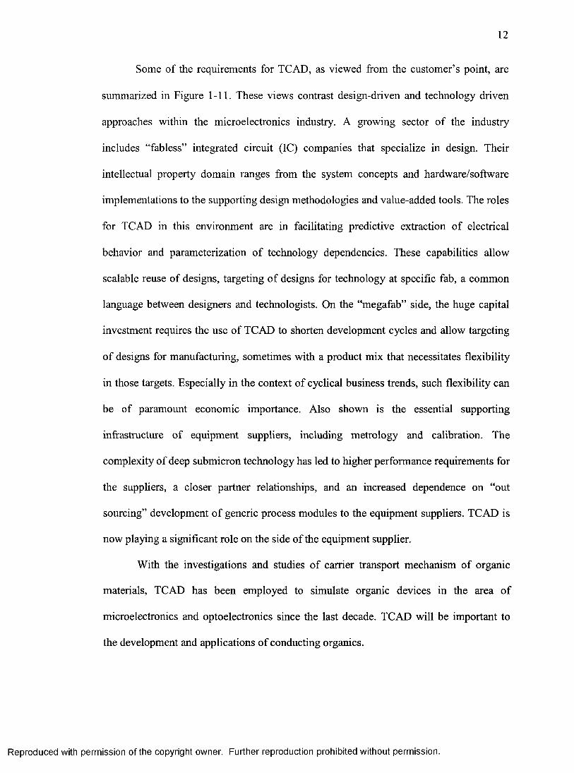
Some o f the requirements for TCAD, as viewed from the customer’s point, are
summarized in Figure 1-11. These views contrast design-driven and technology driven
approaches within the microelectronics industry. A growing sector o f the industry
includes “fabless” integrated circuit (IC) companies that specialize in design. Their
intellectual property domain ranges from the system concepts and hardware/software
implementations to the supporting design methodologies and value-added tools. The roles
for TCAD in this environment are in facilitating predictive extraction o f electrical
behavior and parameterization o f technology dependencies. These capabilities allow
scalable reuse o f designs, targeting o f designs for technology at specific fab, a common
language between designers and technologists. On the “megafab” side, the huge capital
investment requires the use o f TCAD to shorten development cycles and allow targeting
o f designs for manufacturing, sometimes with a product mix that necessitates flexibility
in those targets. Espeeially in the context o f cyclical business trends, such flexibility can
be of paramount economic importance. Also shown is the essential supporting
infrastructure of equipment suppliers, including metrology and calibration. The
complexity o f deep submicron technology has led to higher performance requirements for
the suppliers, a closer partner relationships, and an increased dependence on “out
sourcing” development o f generic process modules to the equipment suppliers. TCAD is
now playing a significant role on the side o f the equipment supplier.
With the investigations and studies o f carrier transport mechanism of organic
materials, TCAD has been employed to simulate organic devices in the area o f
microelectronics and optoelectronics since the last decade. TCAD will be important to
the development and applications o f conducting organics.
Reproduced with permission of the copyright owner. Further reproduction prohibited without permission.
13
Views of TCAD Applications—MegaFab vs. Fabless
Technotogy-DriveiK ^ Integrated (with MegaPabJa Y System Deiiign N / ' Design-DrivenY (possibly Fabless)’(amorliMlion of «»sO \ , Ciiaii(»R&D I •Scalable CeJU ami Libiarks
•l^dictiveVu-tuatFab s<^^ablility)-{ekcUiciy «x<jracti(m) j *Pfe<lk‘tive ElecUieal Sim«la»Km j
•Motlulariiy \ •Parami^cntEable Tecbool^^y-{.soft- anti hajilw«c) *Equlpi})enl SkivuleAK n -(ufiiti«c lcvo^|«)
»<♦ Se»seConCroi)•Infegmtetl Mefrotofy/CalibR^kml
Developmcftt
^ppofiing Jnfra-Simctt
Figure 1-11 TCAD applications in “MegaFab” and “Fabless” environments [26].
1.5 Objectives
The objectives o f this project are to fabricate and simulate the organic
microelectronic devices by traditional lithography process and Technology Computer
Aided Design (TCAD), respectively. In detail:
1. Fabrication and Characterization. Several basic device structures will be
investigated in this project, which include metal-insulator-metal (MIM)
capacitors, metal-insulator-semiconductor (MIS) capacitors, Schottky diodes, and
metal-insulator-semiconductor field-effect transistors (MISFETs). A series of
novel investigations on temperature dependence of mobility and modification at
semiconductor/insulator interface are carried out and discussed.
2. Modeling and Simulation. Currently, the modeling and simulation o f organic
microelectronic devices are very limited due to the unclear mechanisms o f
electrical transport o f organic materials. It is necessary to model and simulate
organic devices to study, analyze, and verify the transport mechanisms o f organic
materials. We will employ TCAD tools MEDICI and Taurus-Device (Synopsys®)
Reproduced with permission of the copyright owner. Further reproduction prohibited without permission.
14
to simulate the fabricated devices and generate the models based on the
experimental results and simulation results.
1.6 Organization of this Dissertation
Chapter One introduces the discovery and development o f organic
microelectronics, the various applications o f conducting and semiconducting organics in
microelectronics, fabrication techniques, conduction mechanism, introduction to TCAD,
and the objectives o f this dissertation. Chapter Two describes the fabrication and
characterization o f capacitors involving organic insulators and semiconductors. Chapter
Three illustrates the construction o f Schottky diodes and TCAD simulation. Chapter Four
details the design, realization and improvement o f organic field-effect transistors
(OFETs). Moreover, a detailed TCAD simulation is carried out based on the fabricated
devices. The conclusion and the work for future studies are addressed in Chapter Five.
Reproduced with permission of the copyright owner. Further reproduction prohibited without permission.
15
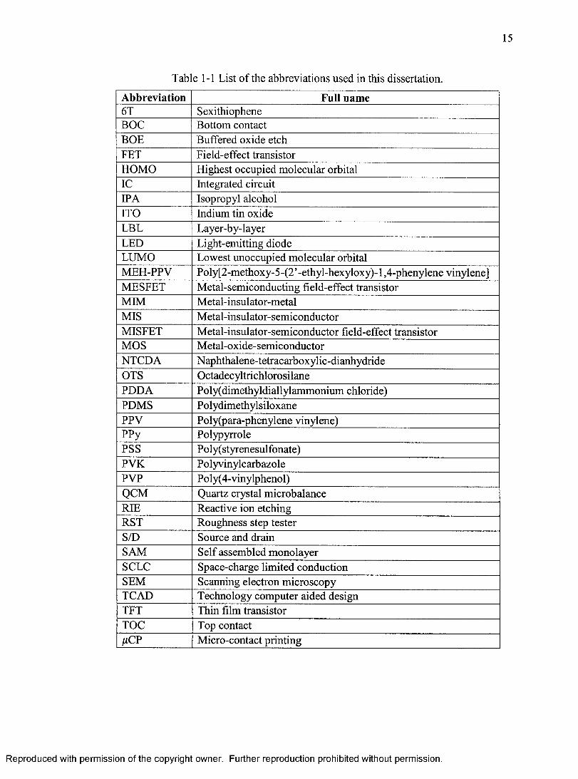
Table 1-1 List of the abbreviations used in this dissertation.
Abbreviation Full name6 T SexithiopheneBOC Bottom contactBOB Buffered oxide etchFET Field-effect transistorHOMO Highest occupied moleeular orbitalIC Integrated cireuitIPA Isopropyl alcoholITO Indium tin oxideLBL Layer-hy-layerLED Light-emitting diodeLUMO Lowest unoceupied molecular orbitalMEH-PPV Poly[2-methoxy-5 -(2 ’ -ethyl-hexyloxy)-1,4-phenylene vinyl ene]MESFET Metal-semiconducting field-effect transistorMIM Metal-insulator-metalMIS Metal-insulator-semiconductorMISFET Metal-insulator-semiconductor field-effect transistorMOS Metal-oxide-semiconductorNTCDA Naphthalene-tetracarboxylic-dianhydrideOTS OctadecyltrichlorosilanePDDA Poly(dimethyIdiallyIammonium chloride)PDMS PolydimethylsiloxanePPV Poly(para-phenylene vinylene)PPy PolypyrrolePSS Poly(styrenesulfonate)PVK Pol5rvinylcarbazoIePVP PoIy(4-vinylphenol)QCM Quartz crystal microbalanceRIE Reactive ion etehingR S I Roughness step testerS/D Source and drainSAM Self assembled monolayerSCLC Spaee-eharge limited eonductionSEM Scanning electron microscopyTCAD Technology computer aided designTFT Thin film transistorTOC Top contact/rCP Micro-contact printing
Reproduced with permission of the copyright owner. Further reproduction prohibited without permission.
CHAPTER TWO
ORGANIC CAPACITORS
2.1 Introduction
Capacitors are basic microelectronic components o f ICs for wireless
communication, memory, etc. Several literatures for organic capacitors consisting of
organic insulators [31][32][33] and conducting polymer [34][35][36] are reported. The
investigation o f organic insulators will benefit the realization o f all organic
microelectronics. In this project, we focus on the fabrication and characterization of
organic insulator. Furthermore, the investigated insulator will be used to construct
organic MIS capacitors and FETs involved. The parameters for the MIS capacitors and
FETs are calculated with the assistance o f the investigated dielectric constant.
2.2 Theory of MIM and MIS Capacitors
2.2.1 Metal-insulator-metal (MIMl Capacitors
A metal-insulator-metal (MIM) capacitor (also known as the parallel-plate
capacitor) is one o f the most common components in electronics, which is composed by
two electrodes sandwiching a layer o f insulator. The following equation describes the
fundamental behavior of a MIM capacitor,
(2- 1)
16
Reproduced with permission of the copyright owner. Further reproduction prohibited without permission.
17
Co is the capacitance, Kj is the dielectric constant o f the insulator, €o is the permittivity o f
free space, d is the thickness o f the insulator (distance between two electrodes), and A is
the area of electrodes.
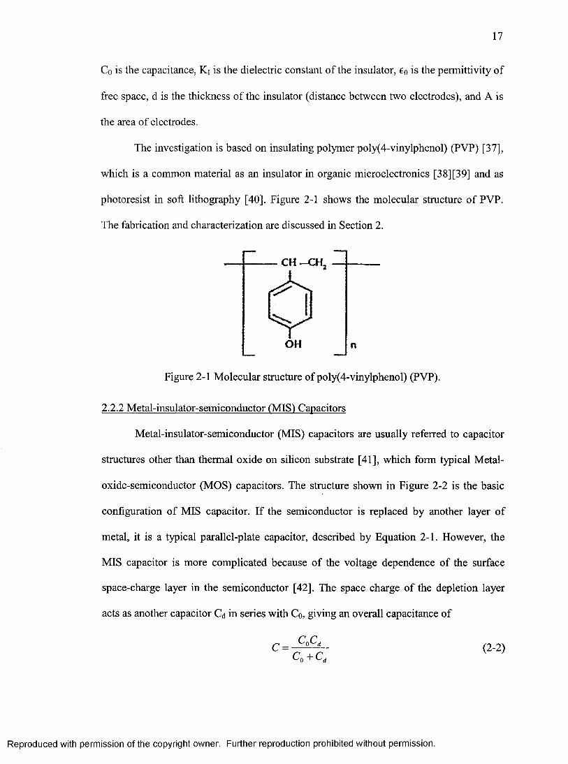
The investigation is based on insulating polymer poly(4-vinylphenol) (PVP) [37],
which is a common material as an insulator in organic microelectronics [38][39] and as
photoresist in soft lithography [40]. Figure 2-1 shows the molecular structure o f PVP.
The fabrication and characterization are discussed in Section 2.
CH -C H ,
OH n
Figure 2-1 Molecular structure o f poly(4-vinylphenol) (PVP).
2.2.2 Metal-insulator-semiconductor (MIS') Capacitors
Metal-insulator-semiconductor (MIS) capacitors are usually referred to capacitor
structures other than thermal oxide on silicon substrate [41], which form typical Metal-
oxide-semiconductor (MOS) capacitors. The structure shown in Figure 2-2 is the basic
configuration o f MIS capacitor. If the semiconductor is replaced by another layer o f
metal, it is a typical parallel-plate capacitor, described by Equation 2-1. However, the
MIS capacitor is more complicated because o f the voltage dependence o f the surface
space-charge layer in the semiconductor [42]. The space charge o f the depletion layer
acts as another capacitor Ca in series with Co, giving an overall capacitance o f
C CC =
Co+C,(2-2)
Reproduced with permission of the copyright owner. Further reproduction prohibited without permission.
18
The capacitance o f depletion layer is
(2 -3 )
where Ks is the dielectric constant o f the semiconductor and xa is the thickness o f the
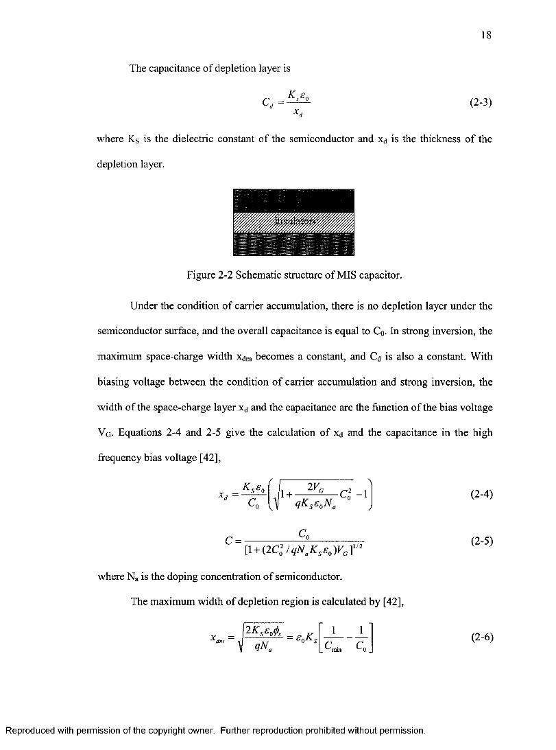
depletion layer.
Figure 2-2 Schematic structure o f MIS capacitor.
Under the condition o f carrier accumulation, there is no depletion layer under the
semiconductor surface, and the overall capacitance is equal to Co- In strong inversion, the
maximum space-charge width Xdm becomes a constant, and Ca is also a constant. With
biasing voltage between the condition o f carrier accumulation and strong inversion, the
width o f the space-charge layer xa and the capacitance are the function o f the bias voltage
Vg- Equations 2-4 and 2-5 give the calculation o f xa and the capacitance in the high
frequency bias voltage [42],
L . Q - 1
c[\ + { 2 C l l q N ^ K , s , ) V j ' ^
where Na is the doping concentration o f semiconductor.
The maximum width o f depletion region is calculated by [42],
(2-4)
(2-5)
Xdn, =1 1
C C ' - '0
(2-6)
Reproduced with permission of the copyright owner. Further reproduction prohibited without permission.
19
where Cmin is the minimum capaeitance and surfaee potential 4 >s is,
(!>s = 2 ^^ + 6(1) (2-7)
as the condition o f the onset o f strong inversion o f carrier. (|)f is the difference between
the midgap Ei and the Fermi level Ef in the bulk o f the semiconductor,
<Pf=<l>T l n ( — ) (2-8)
with (j>j. = kT I q . Since kT represents the thermal energy at temperature T, 4>i is
considered as the voltage equivalent o f temperature, k is the Boltzmann’s constant and ni
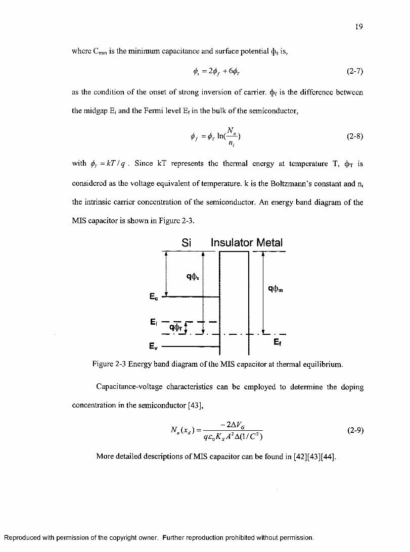
the intrinsic carrier concentration o f the semiconductor. An energy band diagram of the
MIS capacitor is shown in Figure 2-3.
Si Insulator Metal
q4>«
Figure 2-3 Energy band diagram of the MIS capacitor at thermal equilibrium.
Capaeitance-voltage characteristics can be employed to determine the doping
concentration in the semiconductor [43],
- 2 A F.q£oKsA^A(l/C^)
(2-9)
More detailed descriptions o f MIS capacitor can be found in [42][43][44].
Reproduced with permission of the copyright owner. Further reproduction prohibited without permission.
2 0
2.3 Capacitors with Organic Insulator
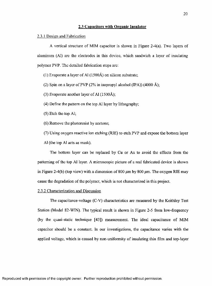
2.3.1 Design and Fabrication
A vertical structure o f MIM capacitor is shown in Figure 2-4(a). Two layers o f
aluminum (Al) are the electrodes in this device, which sandwich a layer o f insulating
polymer PVP. The detailed fabrication steps are:
(1) Evaporate a layer o f Al (ISOOA) on silicon substrate;
(2) Spin on a layer o f PVP (2% in isopropyl alcohol (IPA)) (4000 A);
(3) Evaporate another layer o f Al (1500A);
(4) Define the pattern on the top Al layer by lithography;
(5) Etch the top Al;
(6 ) Remove the photoresist by acetone;
(7) Using oxygen reactive ion etching (RIE) to etch PVP and expose the bottom layer
Al (the top Al acts as mask).
The bottom layer can be replaced by Cu or An to avoid the effects from the
patterning of the top Al layer. A microscopic picture o f a real fabricated device is shown
in Figure 2-4(b) (top view) with a dimension of 800 jum by 800 jum. The oxygen RIE may
cause the degradation o f the polymer, which is not characterized in this project.
2.3.2 Characterization and Discussion
The capacitance-voltage (C-V) characteristics are measured by the Keithley Test
Station (Model 82-WIN). The typical result is shown in Figure 2-5 from low-frequency
(by the quasi-static technique [43]) measurement. The ideal capacitance o f MIM
capacitor should be a constant. In our investigations, the capacitance varies with the
applied voltage, which is caused by non-uniformity o f insulating thin film and top-layer
Reproduced with permission of the copyright owner. Further reproduction prohibited without permission.
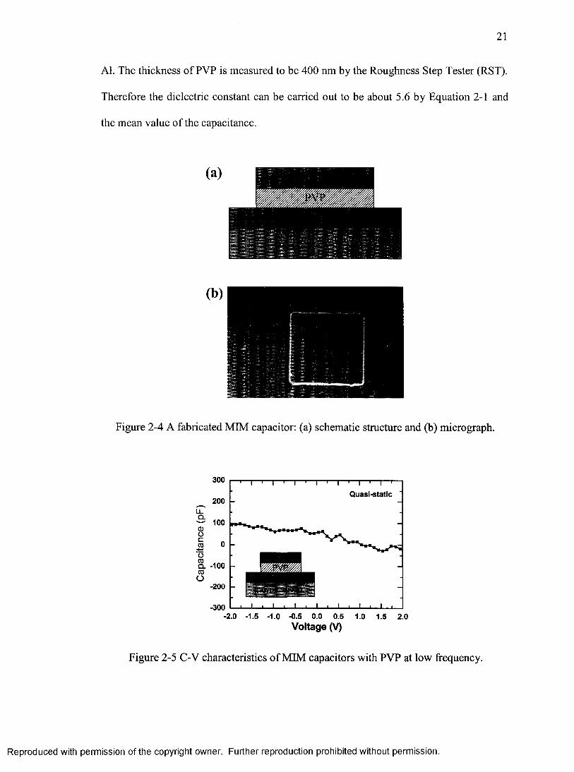
21
Al. The thickness o f PVP is measured to be 400 nm by the Roughness Step Tester (RST).
Therefore the dielectric constant can be carried out to be about 5.6 by Equation 2-1 and
the mean value o f the capacitance.
Figure 2-4 A fabricated MIM capacitor: (a) schematic structure and (b) micrograph.
300
LLQ.0OCCD
200 -
100
0 -
oroCL -100CDo
-200
-r->—I—'—r -I—I—I—p-i—I—r-Quasi-static
■300 __' I I I I I ' I I I I I ■ I ■-2.0 -1.5 -1.0 -0.5 0.0 0.5 1.0 1.5 2.0
Voltage (V)
Figure 2-5 C-V characteristics o f MIM capacitors with PVP at low frequency.
Reproduced with permission of the copyright owner. Further reproduction prohibited without permission.
2 2
2.3.3 Verification
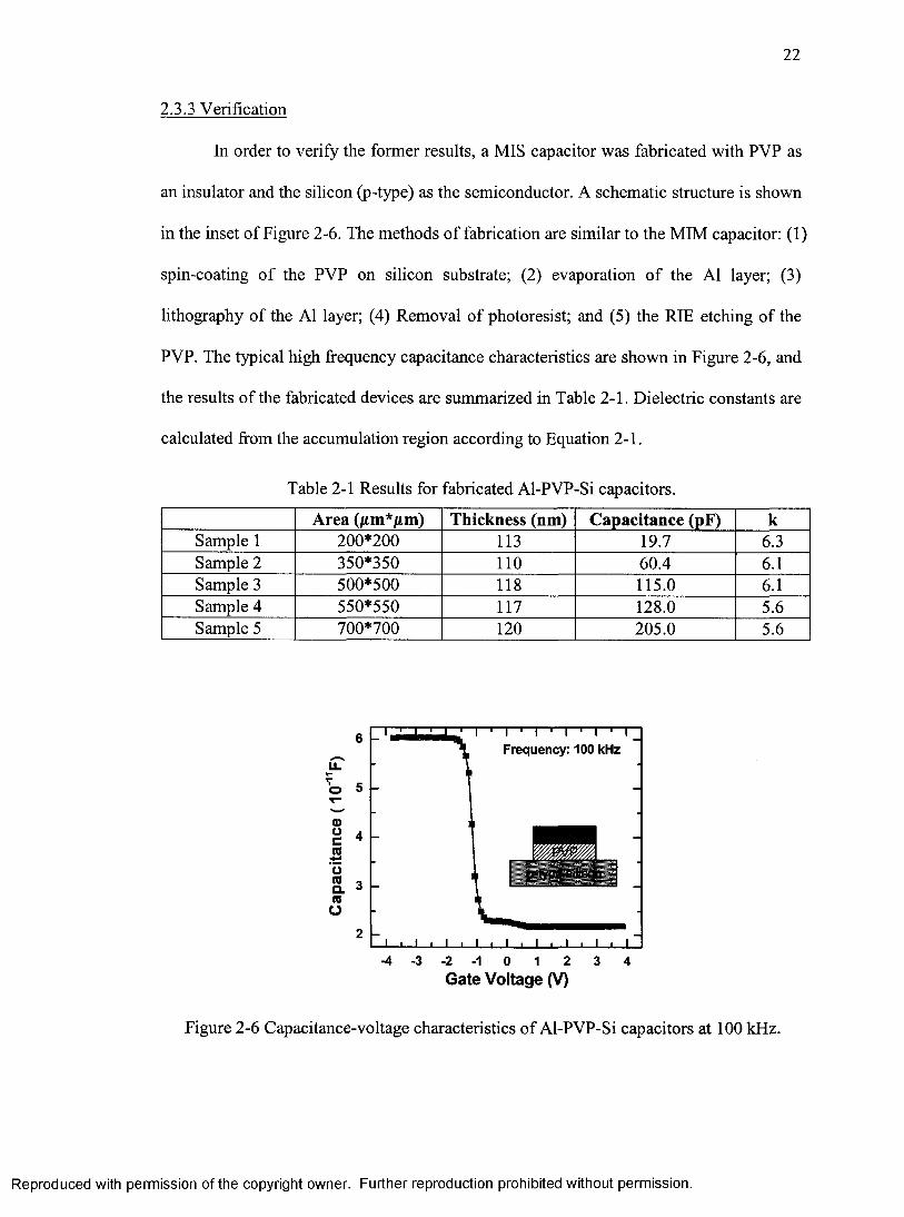
In order to verify the former results, a MIS capacitor was fabricated with PVP as
an insulator and the silicon (p-type) as the semiconductor. A schematic structure is shown
in the inset o f Figure 2-6. The methods o f fabrication are similar to the MIM capacitor: (1)
spin-coating o f the PVP on silicon substrate; (2) evaporation o f the Al layer; (3)
lithography o f the Al layer; (4) Removal o f photoresist; and (5) the RIE etching o f the
PVP. The typical high frequency capacitance characteristics are shown in Figure 2-6, and
the results o f the fabricated devices are summarized in Table 2-1. Dielectric constants are
calculated from the accumulation region according to Equation 2-1.
Table 2-1 Results for fabricated Al-PVP-Si capacitors.
Area Thickness (nm) Capacitance (pF) kSample 1 2 0 0 * 2 0 0 113 19.7 6.3Sample 2 350*350 n o 60.4 6 . 1
Sample 3 500*500 118 II5 .0 6 . 1
Sample 4 550*550 117 128.0 5.6Sample 5 700*700 1 2 0 205.0 5.6
ju .
o 5
0)oc(0o(0Q.CQO
I ' I ' I ' I ' I ' I Frequency: 100 kHz
up-type silicon
I ■ I ■ I ......................I l l- 4 - 3 - 2 - 1 0 1 2 3 4
Gate Voltage (V)
Figure 2-6 Capacitance-voltage characteristics o f Al-PVP-Si capacitors at 100 kHz.
Reproduced with permission of the copyright owner. Further reproduction prohibited without permission.
23
The values o f the dielectric constant range from 5.6 to 6.3, which are consistent
with the former results from Al-PVP-Al structure, about 5.6. The mean value and
standard deviation o f dielectric constants are 5.94 and 0.32, respectively, in the aspect of
statistics for the data in Table 2-1. This result is more trustable than what we carried out
in the last section because o f a fewer fabrication steps are involved and the capacitance
curves are more stable.
2.4 Capacitors with Oreanic Semiconductor
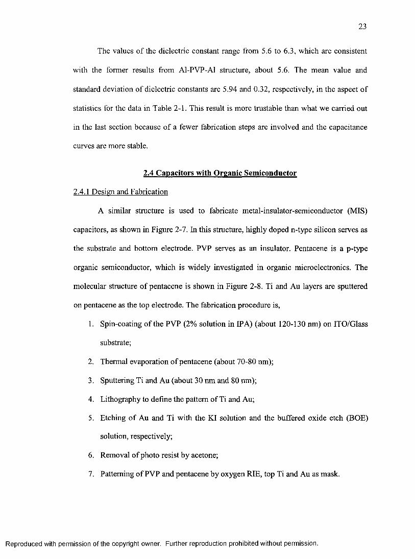
2.4.1 Design and Fabrication
A similar structure is used to fabricate metal-insulator-semiconductor (MIS)
capacitors, as shown in Figure 2-7. In this structure, highly doped n-type silicon serves as
the substrate and bottom electrode. PVP serves as an insulator. Pentacene is a p-type
organic semiconductor, which is widely investigated in organic microelectronics. The
molecular structure o f pentacene is shown in Figure 2-8. Ti and Au layers are sputtered
on pentacene as the top electrode. The fabrication procedure is,
1. Spin-coating o f the PVP (2% solution in IPA) (about 120-130 nm) on ITO/Glass
substrate;
2. Thermal evaporation o f pentacene (about 70-80 nm);
3. Sputtering Ti and Au (about 30 nm and 80 nm);
4. Lithography to define the pattern o f Ti and Au;
5. Etching of Au and Ti with the KI solution and the buffered oxide etch (BOE)
solution, respectively;
6 . Removal o f photo resist by acetone;
7. Patterning o f PVP and pentacene by oxygen RIE, top Ti and Au as mask.
Reproduced with permission of the copyright owner. Further reproduction prohibited without permission.
24
H ighly Doped Si
Figure 2-7 Schematic structure o f MIS capacitors with organic semiconductor.
Figure 2-8 Molecular structiorc o f pentacene.
2.4.2 Characterization and Discussion
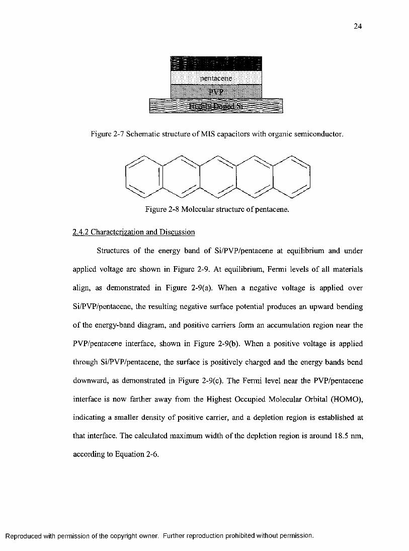
Structures o f the energy band of Si/PVP/pentacene at equilibrium and under
applied voltage are shown in Figure 2-9. At equilibrium, Fermi levels o f all materials
align, as demonstrated in Figure 2-9(a). When a negative voltage is applied over
Si/PVP/pentacene, the resulting negative surface potential produces an upward bending
o f the energy-hand diagram, and positive carriers form an accumulation region near the
PVP/pentacene interface, shown in Figure 2-9(b). When a positive voltage is applied
through Si/PVP/pentacene, the surface is positively charged and the energy bands bend
downward, as demonstrated in Figure 2-9(c). The Fermi level near the PVP/pentacene
interface is now farther away from the Highest Occupied Molecular Orbital (HOMO),
indicating a smaller density o f positive carrier, and a depletion region is established at
that interface. The calculated maximum width o f the depletion region is around 18.5 nm,
according to Equation 2-6.
Reproduced with permission of the copyright owner. Further reproduction prohibited without permission.
25
Ti/Au pentacene PVP n"" Si Ti/Au pentacene PVP n"" SI Ti/Au pentacene PVP n"" SiEvacuum
Ss
3.2 eVE•vacuum
4
|3.2 eV
s LUMO
4.8 eV4.1 eV
^ | l u m o
5.0 eV 5.0 eV
E c■
HOMO(l>)
HOMO
4.8 eV
— - Ef Vg < 0
(c)
3.2 eV
LUMO
N
HOMO
P> 4.1 eV
IVg > 0 - ■ Ef
Figure 2-9 Energy band o f pentacene MIS capacitors.
421.0
gO.939
0.7
36 0.6
Voltage (V)
33Q.Frequency: 100 kHz
30-6 -4 ■2 0 2 4 6 8
Voltage (V)
Figure 2-10 C-V characteristics o f metal-PVP-pentacene structure at high frequency.
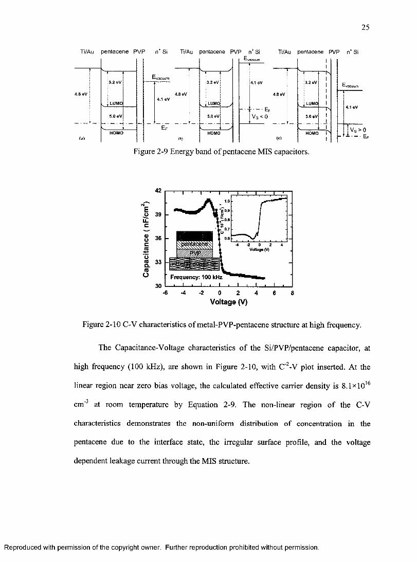
The Capacitance-Voltage characteristics o f the Si/PVP/pentacene capacitor, at
high frequency (100 kHz), are shown in Figure 2-10, with C‘ -V plot inserted. At the
linear region near zero bias voltage, the calculated effective carrier density is S.lxlO '^
cm'^ at room temperature by Equation 2-9. The non-linear region o f the C-V
characteristics demonstrates the non-uniform distribution of concentration in the
pentacene due to the interface state, the irregular surface profile, and the voltage
dependent leakage current through the MIS structure.
Reproduced with permission of the copyright owner. Further reproduction prohibited without permission.
CHAPTER THREE
ORGANIC SCHOTTKY DIODES
3.1 Introduction
Poly[2-methoxy-5-(2’-ethyl-hexyloxy)-l,4-phenylene vinylene]) (MEH-PPV) is a
poly(para-phenylene vinylene) (PPV) derived p-type polymer which is among the most
popular materials used to build OTFTs and OLEDs [51][52][53j. The molecular structure
o f MEH-PPV is shown in Figure 3-1. Several studies have been carried out for Schottky
diodes by MEH-PPV and various metals [54][55] [56]. The characteristics o f Schottky
contact between polymer and metal are important to investigate both material properties
and interface characteristics. The temperature and electric field dependent mobility of
MEH-PPV was studied in the literature [57] [5 8 ].
However, the mobility behavior o f MEH-PPV above room temperature has not
been reported to our knowledge. In this work, experimental and theoretical efforts have
been carried out to investigate the mobility behavior above room temperature, based on
the current density-voltage (J-V) characteristics and capacitance-voltage (C-V)
characteristics o f ITO/MEH-PPV/Al Schottky diodes. The highest mobility is obtained at
about 353 K. The space-charge limited conduction (SCLC) model [59] and the field-
dependent relationship have been employed to extract mobility values. The value o f the
effective hole density has been determined to be 2.24x lO'^ cm'^.
26
Reproduced with permission of the copyright owner. Further reproduction prohibited without permission.
27
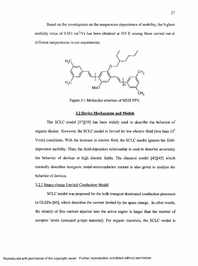
Based on the investigation on the temperature dependence of mobility, the highest
• • 2 mobility value of 0.013 cm /Vs has been obtained at 353 K among those carried out at
different temperatures in our experiments.
HX
CH
N XMeO
CH3
Figure 3-1 Molecular structure o f MEH-PPV.
3.2 Device Mechanisms and Models
The SCLC model [57][59] has been widely used to describe the behavior of
organic diodes. However, the SCLC model is limited for low electric field (less than 10
V/cm) conditions. With the increase in electric field, the SCLC model ignores the field-
dependent mobility. Thus, the field-dependent relationship is used to describe accurately
the behavior of devices at high electric fields. The classical model [42] [43] which
normally describes inorganic metal-semiconductor contact is also given to analyze the
behavior o f devices.
3.2.1 Space-charge Limited Conduction Model
SCLC model was proposed for the bulk transport dominated conduction processes
in OLEDs [60], which describes the current limited by the space charge. In other words,
the density o f free carriers injected into the active region is larger than the number o f
acceptor levels (assumed p-type material). For organic materials, the SCLC model is
Reproduced with permission of the copyright owner. Further reproduction prohibited without permission.
28
expected to be applicable due to relatively small acceptor density and small mobility of
the carriers. The model is described by the following equation:
9
where J is the current density, V is the voltage, fo^r is the permittivity o f the polymer, (ip
is the hole mobility (assumed p-type conducting polymer), and L is the device thickness.
The SCLC regime occurs when the equilibrium charge concentration (before
charge injection) is negligible compared to the injected charge concentration. This will
form a space charge region near the injecting electrode with the concentration of the
space charge rapidly ending away from the electrode. In this space charge regime, the
current is proportional to the square o f the electric field.
3.2.2 Field-dependent Relationship
Field-dependent models are used to describe the hole mobility in MEH-PPV when
the electric field is high (larger than 10 V/cm), and the constant mobility in the SCLC
model is no longer applicable. The characteristics o f current density versus voltage can be
described by the equation:
J = p(x)ejUp[E{x)]E(x) (3-2)
with the field-dependent mobility given by
Mp (E) = Mp (0) qM y 4 e ) (3-3)
where the zero field mobility is given by
/^p(0) = / ^ o e x p ( - ^ ) (3-4)
and
Reproduced with permission of the copyright owner. Further reproduction prohibited without permission.
1 1
k j k j ^ )
29
(3-5)
and where p(x) is the density o f the hole concentration at position x, E(x) is the electric
field at position x, po is a constant prefactor, E* is the activation energy, and To and B are
material constants which are equal to 600 K and 2.9X10'^ eV(m/V)'''^ for MEH-PPV,
respectively [57].
3.2.3 Classical Model
When a forward bias voltage is applied, the potential barrier from the
semiconductor to metal is reduced which favors the carrier transport from the
semiconductor to the metal. The current is described in [43],
expv - i - n
n(f).- 1 (3-6)
and
I q = AA**T^ exp -<Pb (3-7)\ TT Jwhere A is the junction area. A** is the Richardson constant, T is the temperature in
Kelvins, Rs is the series resistance, is the thermal voltage at certain temperature which
is equal Xo kT I q , is the barrier height, n is the ideality factor, and Iq is the reverse
saturation current.
3.3 Fabrication Approach
MEH-PPV (American Dye Source, Inc.) 0.2% wt solution was prepared on
tetrahydrofuran. Glass substrate is covered by a deposited layer o f ITO thin film (60 A).
After substrate cleaning by acetone and deionized water, MEH-PPV was deposited on the
Reproduced with permission of the copyright owner. Further reproduction prohibited without permission.
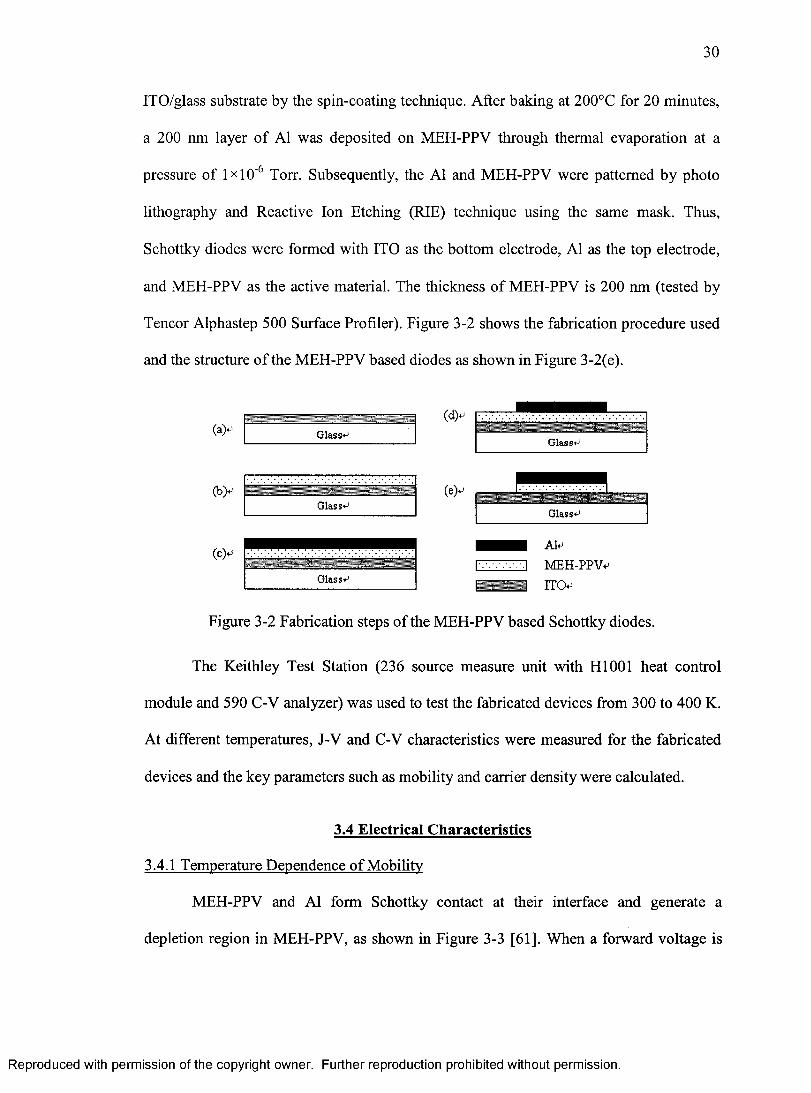
30
ITO/glass substrate by the spin-eoating technique. After baking at 200°C for 20 minutes,
a 200 nm layer o f Al was deposited on MEH-PPV through thermal evaporation at a
pressure o f 1x10'^ Torr. Subsequently, the Al and MEH-PPV were patterned by photo
lithography and Reactive Ion Etehing (RIE) technique using the same mask. Thus,
Schottky diodes were formed with ITO as the bottom electrode, Al as the top electrode,
and MEH-PPV as the active material. The thickness o f MEH-PPV is 200 nm (tested by
Tencor Alphastep 500 Surface Profiler). Figure 3-2 shows the fabrication procedure used
and the structure o f the MEH-PPV based diodes as shown in Figure 3-2(e).
(a)* Glass<J
Glass-*
(d)
(e).
Glass+-'
Glass^
(c).
Glass*
Al^I-. . .I MEH-PPV^
rro^
Figure 3-2 Fabrication steps o f the MEH-PPV based Schottky diodes.
The Keithley Test Station (236 source measure unit with HlOOl heat control
module and 590 C-V analyzer) was used to test the fabricated devices from 300 to 400 K.
At different temperatures, J-V and C-V characteristics were measured for the fabricated
devices and the key parameters such as mobility and carrier density were calculated.
3.4 Electrical Characteristics
3.4.1 Temperature Dependence o f Mobilitv
MEH-PPV and Al form Schottky contact at their interface and generate a
depletion region in MEH-PPV, as shown in Figure 3-3 [61]. When a forward voltage is
Reproduced with permission of the copyright owner. Further reproduction prohibited without permission.
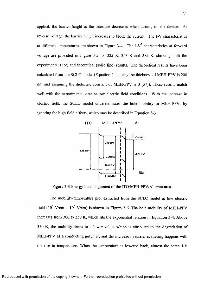
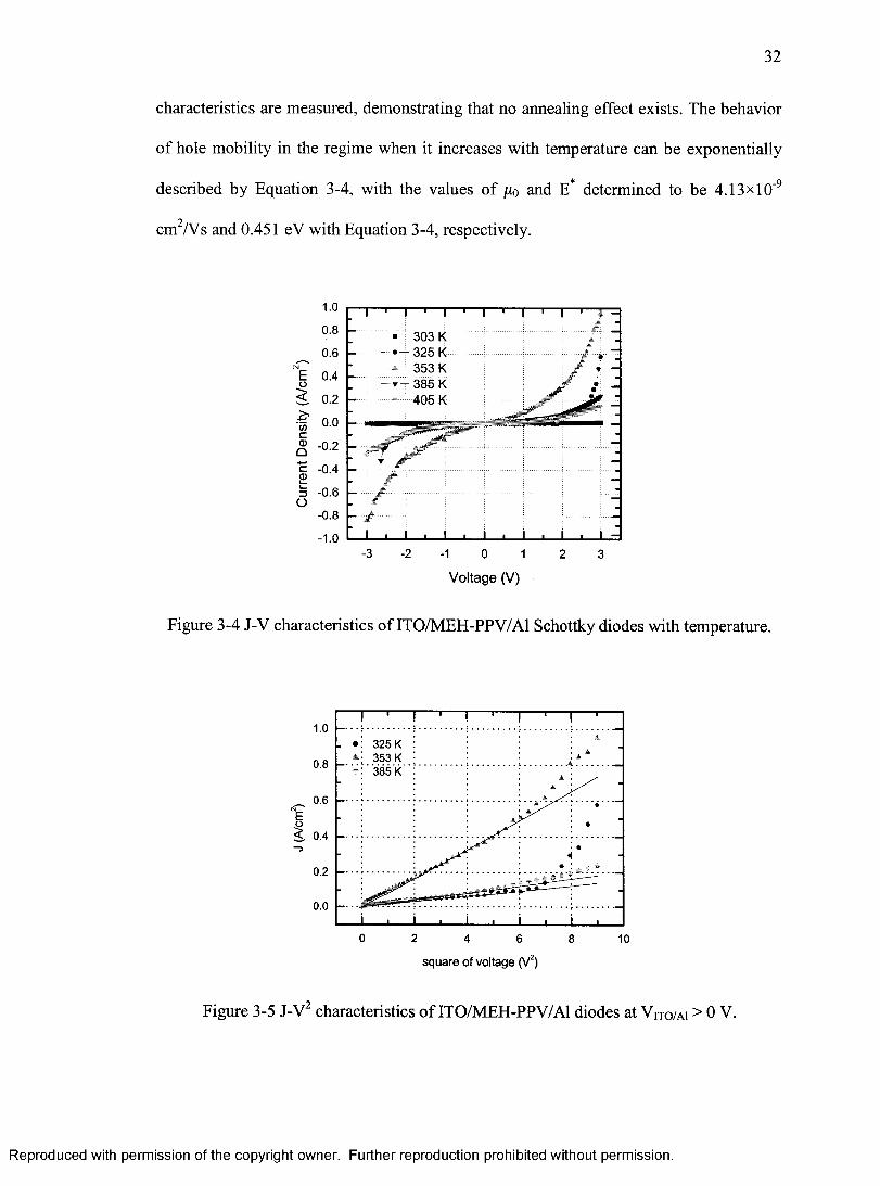
31
applied, the barrier height at the interface decreases when turning on the device. At
reverse voltage, the barrier height increases to block the current. The J-V characteristics
at different temperatures are shown in Figure 3-4. The J-V^ characteristics at forward
voltage are provided in Figure 3-5 for 325 K, 353 K and 385 K, showing both the
experimental (dot) and theoretical (solid line) results. The theoretical results have been
calculated from the SCLC model (Equation 2-1, using the thickness o f MEH-PPV is 200
nm and assuming the dielectric constant o f MEH-PPV is 3 [57]). These results match
well with the experimental data at low electric field conditions. With the increase in
electric field, the SCLC model underestimates the hole mobility in MEH-PPV, by
ignoring the high field effects, which may be described in Equation 3-3.
ITO M EH -PPV Al11
1"^c -vacuum
2 .9 eV11
4 .8 eV
V. , LUMO
111
4.1 eV
5 .3 eV1
V. 1 EHOMO l ^
1
Figure 3-3 Energy-band alignment o f the ITO/MEH-PPV/Al structures.
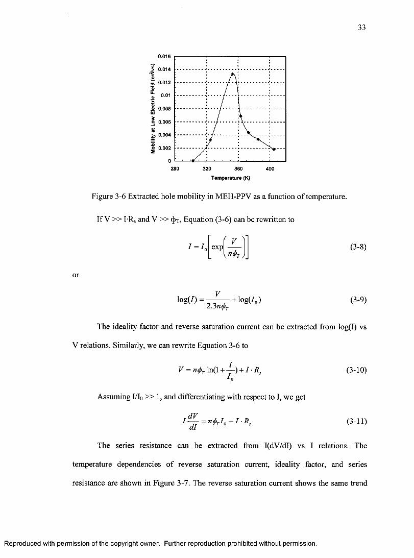
The mobility-temperature plot extracted from the SCLC model at low electric
field (10^ V/cm - 10 V/cm) is shown in Figure 3-6. The hole mobility o f MEH-PPV
increases from 300 to 350 K, which fits the exponential relation in Equation 3-4. Above
350 K, the mobility drops to a lower value, which is attributed to the degradation of
MEH-PPV as a conducting polymer, and the increase in carrier scattering happens with
the rise in temperature. When the temperatme is lowered back, almost the same J-V
Reproduced with permission of the copyright owner. Further reproduction prohibited without permission.
32
characteristics are measured, demonstrating that no annealing effect exists. The behavior
of hole mobility in the regime when it increases with temperature can be exponentially
described by Equation 3-4, with the values o f jXo and E* determined to be 4.13x10'^
cm^/Vs and 0.451 eV with Equation 3-4, respectively.
0.8 -■ --3 0 3 K • 325 K** 4 353 k
0.6CN
E 0.4 o 0.2385 k 405 K
I 0.0
(§ -0-2
-0.44 -*cE
- 0.63O- 0.8
- 1.0■3 •2 1 0 1 2 3
Voltage (V)
Figure 3-4 J-V characteristics o f ITO/MEH-PPV/Al Schottky diodes with temperature.
325 K 353 K385 K
'EoE . 0.4-3
0.2
0.0
0 2 4 6 8 10
sq u a re of voltage (V )
Figure 3-5 J-V characteristics o f ITO/MEH-PPV/Al diodes at V ito /a i > 0 V.
Reproduced with permission of the copyright owner. Further reproduction prohibited without permission.
33
0.016
> 0.014
5 0.012 .2O 0.01
s> 0.008ui3o_i 0.006
150.004
I 0.002
280 320 360 400
Temperature (K)
Figure 3-6 Extracted hole mobility in MEH-PPV as a function o f temperature.
If V » I Rs and V » Equation (3-6) can be rewritten to
I = L exp (3-8)
or
log(/) = + lo g (^ ) (3-9)23n(j)j.
The ideality factor and reverse saturation current can be extracted from log(I) vs
V relations. Similarly, we can rewrite Equation 3-6 to
F = «^^^ln(l + — ) + /-i?^
Assuming EIo » 1, and differentiating with respect to I, we get
f d V . r r u
(3-10)
(3-11)
The series resistance can be extracted from I(dV/dI) vs I relations. The
temperature dependencies o f reverse saturation current, ideality factor, and series
resistance are shown in Figure 3-7. The reverse saturation current shows the same trend
Reproduced with permission of the copyright owner. Further reproduction prohibited without permission.
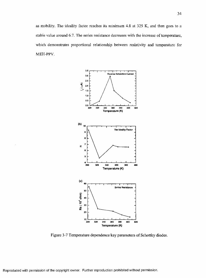
34
as mobility. The ideality factor reaches its minimum 4.8 at 325 K, and then goes to a
stable value around 6.7. The series resistance decreases with the increase o f temperature,
which demonstrates proportional relationship between resistivity and temperature for
MEH-PPV.
3.5Reverse Saturation Current '
3.0 -
2.5
^ 2.0 -
1.5
1.0
0.5
0.0300 320 340 360 380 400 420
Temperature (K)
(b) 10
The Ideality Factor9
8
7
6
5
4300 320 360340 380 400
Temperature (K)
60
Series Resistance50
o 40
w 30
300 320 340 380360 400 420
Temperature (K)
Figure 3-7 Temperature dependence key parameters o f Schottky diodes.
Reproduced with permission of the copyright owner. Further reproduction prohibited without permission.
35
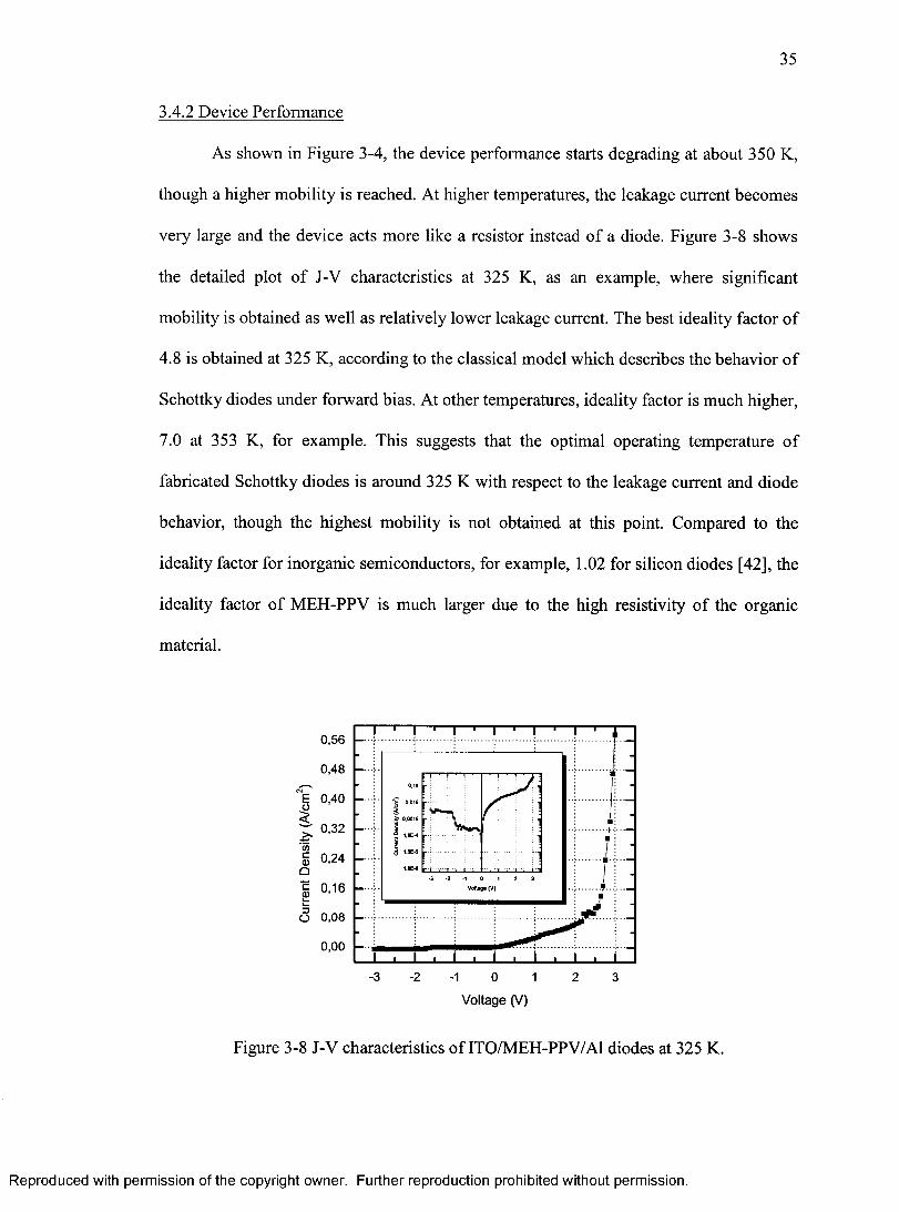
3.4.2 Device Performance
As shown in Figure 3-4, the device performance starts degrading at about 350 K,
though a higher mobility is reached. At higher temperatures, the leakage current becomes
very large and the device acts more like a resistor instead o f a diode. Figure 3-8 shows
the detailed plot o f J-V characteristics at 325 K, as an example, where significant
mobility is obtained as well as relatively lower leakage current. The best ideality factor o f
4.8 is obtained at 325 K, according to the classical model which describes the behavior o f
Schottky diodes under forward bias. At other temperatures, ideality factor is much higher,
7.0 at 353 K, for example. This suggests that the optimal operating temperature o f
fabricated Schottky diodes is around 325 K with respect to the leakage current and diode
behavior, though the highest mobility is not obtained at this point. Compared to the
ideality factor for inorganic semiconductors, for example, 1.02 for silicon diodes [42], the
ideality factor o f MEH-PPV is much larger due to the high resistivity o f the organic
material.
O5
COc0Q
£D
0,56
0,48
0,40
0,32
0,24
0,16
0,08
0,00
-3 -2 -1 0 1
Voltage (V)
Figure 3-8 J-V characteristics o f ITO/MEH-PPV/Al diodes at 325 K.
Reproduced with permission of the copyright owner. Further reproduction prohibited without permission.
36
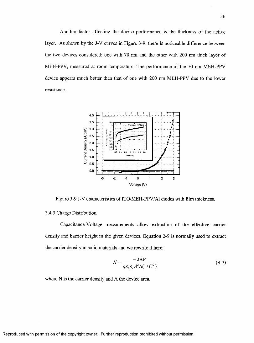
Another factor affecting the device performance is the thickness o f the active
layer. As shown by the J-V curves in Figure 3-9, there is noticeable difference between
the two devices considered: one with 70 nm and the other with 200 nm thick layer of
MEH-PPV, measured at room temperature. The performance o f the 70 nm MEH-PPV
device appears much better than that o f one with 200 nm MEH-PPV due to the lower
resistance.
4,0
3.5 100.. -i.... Thickness .=. 70 .nm:..
.-3 .0Oi , 2.5
2.0c0>Q 1.5
0.01IE-3IE-4
IE-5IE-6IE-7
C0
^ 0.5
0.0
■3 •2 1 0 1 2 3
V oltage (V)
Figure 3-9 J-V characteristics of ITO/MEH-PPV/Al diodes with film thickness.
3.4.3 Charge Distribution
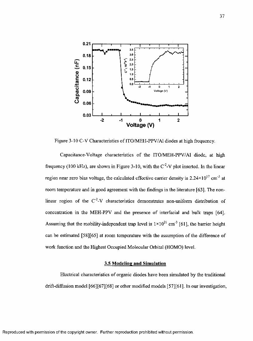
Capacitance-Voltage measurements allow extraction o f the effective carrier
density and barrier height in the given devices. Equation 2-9 is normally used to extract
the carrier density in solid materials and we rewrite it here:
- 2 A VN =
qs^s^A^A{\!C^)
where N is the carrier density and A the device area.
(3-7)
Reproduced with permission of the copyright owner. Further reproduction prohibited without permission.
37
0.213.5
3.0
-j" 2.50.18
u_S 0.15(1>o£ 0 - 1 2 (0
1.5o1.0
0.5
0.0O(0 0.09a<0^ 0.06
Voltage (V)
0.03■2 1 0 1 2
Voltage (V)
Figure 3-10 C-V Characteristics o f ITO/MEH-PPV/Al diodes at high frequency.
Capacitance-Voltage characteristics o f the ITO/MEH-PPV/Al diode, at high
frequency (100 kHz), are shown in Figure 3-10, with the C'^-V plot inserted. In the linear
region near zero bias voltage, the calculated effective carrier density is 2.24x10'^ cm'^ at
room temperature and in good agreement with the findings in the literature [63]. The non
linear region of the C'^-V characteristics demonstrates non-uniform distribution o f
concentration in the MEH-PPV and the presence o f interfacial and bulk traps [64],
Assuming that the mobility-independent trap level is 1x10^' cm'^ [61], the barrier height
can be estimated [58] [65] at room temperature with the assumption o f the difference of
work function and the Highest Occupied Molecular Orbital (HOMO) level.
3.5 Modeling and Simulation
Electrical characteristics o f organic diodes have been simulated by the traditional
drift-diffusion model [66][67][68] or other modified models [57][61]. In our investigation.
Reproduced with permission of the copyright owner. Further reproduction prohibited without permission.
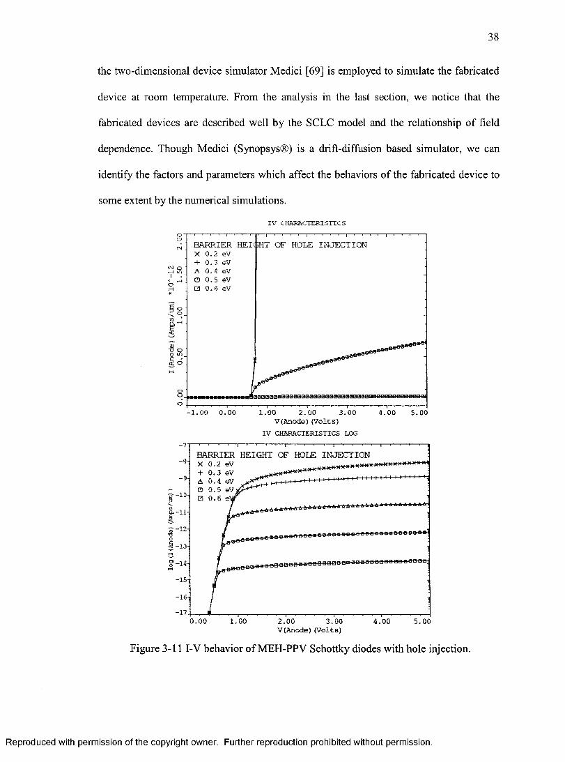
38
the two-dimensional device simulator Medici [69] is employed to simulate the fabricated
device at room temperature. From the analysis in the last section, we notice that the
fabricated devices are described well by the SCLC model and the relationship o f field
dependence. Though Medici (Sjmopsys®) is a drift-diffusion based simulator, we can
identify the factors and parameters which affect the behaviors o f the fabricated device to
some extent by the numerical simulations.
IV CHARACTERISTICS
BARRIER HEIGHT OF HOLE INJECTIONX 0 .2 eV
CM
o
o
- 1 . 0 0 0 . 0 0 1 .0 0 2 . 0 0 3 .0 0 4 .0 0 5 .0 0V (A node) (V o l ts )
IV CHARACTERISTICS LOG
-TBARRIER HEIGHT OT HOLE INJECTIONX 0 .2 eV -(- 0 .3 eV
.00-
-15-
-16-
-17,0 .0 0 1.00 2 .0 0 3 .0 0 4 .0 0 5 .0 0
V (A n o d e )(V o lts )
Figure 3-11 I-V behavior o f MEH-PPV Schottky diodes with hole injection.
Reproduced with permission of the copyright owner. Further reproduction prohibited without permission.
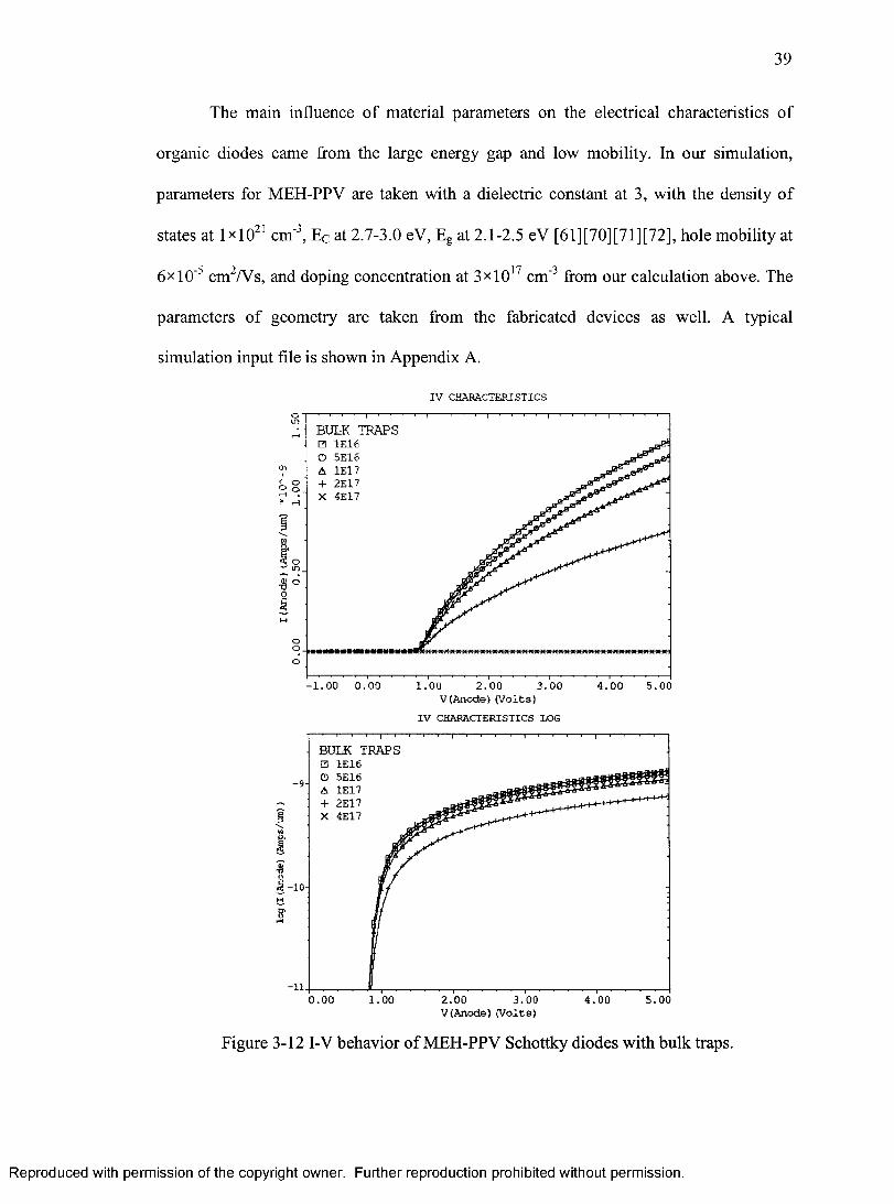
39
The main influence o f material parameters on the electrical characteristics o f
organic diodes came from the large energy gap and low mobility. In our simulation,
parameters for MEH-PPV are taken with a dielectric constant at 3, with the density o f
states at IxfO^^ cm■^ Ec at 2.7-3.0 eV, Eg at 2.1-2.5 eV [61][70][71][72], hole mobility at
6x10’ cm^/Vs, and doping concentration at 3x10^^ cm'^ from our calculation above. The
parameters o f geometry are taken from the fabricated devices as well. A typical
simulation input file is shown in Appendix A.
IV CHARACTERISTICS
BULK TRAPS B 1E16 O 5E16 A 1E17 + 2E17 X 4E17
- 1 . 00 0 . 0 0 1 . 0 0 2 . 0 0 3 .0 0 4 .0 0 5 .0 0V(Anode) (V o lts )
IV CHARACTERISTICS LOG
BULK TRAPS 0 1EI6 O 5E16 A 1E17 + 2E17 X 4E17
-9-
1 - 10-
- 11 ,
4 .0 0 5 .0 00 . 0 0 1 . 0 0 2 . 0 0 3 .0 0V(Anode) (V o lts)
Figure 3-12 I-V behavior o f MEH-PPV Schottky diodes with bulk traps.
Reproduced with permission of the copyright owner. Further reproduction prohibited without permission.
40
A1 is the material o f cathode and its work function is 4.1-4.3 eV. ITO serves as an
anode whose work function varies in a wide range, typically from 4.7 eV to 5.1 eV
[55][61][73][74]. Figure 3-11 (linear upper and logarithm lower) shows the I-V
characteristics o f the device with different work function of the anode, from 4.7 eV to 5.1
eV, corresponding to barrier o f the hole injection from 0.6 eV to 0.2 eV according to Ey
at 5.3 eV. The simulation results are almost the same for 0.2 eV to 0.4 eV barrier heights.
The current flow is limited by the space charge for these cases with small barriers for the
hole injection. As the barrier for the hole injection is further increased, the current is
decreased rapidly, indicating that the current is limited by the injection.
The bulk traps within semiconducting polymer also limit current flow. Figure 3-
12 shows the I-V characteristics o f the device with increasing bulk traps. We notice that
when the traps are small compared to the hole density in MEH-PPV, its effect is
negligible. As traps increase to near the doping concentration, the current flow decreases
dramatically due to significant trapping.
By adjusting the work function o f the anode and the amount o f bulk traps, Figure
3-13 shows a comparison o f I-V characteristics between simulation and measurement.
The hole injection from ITO is chosen to be 0.3 eV for the barrier height, Ec is 2.8 eV, Eg
is 2.2 eV, and bulk traps are chosen to be 3x10^^ cm'^. Simulation results match
experimental results well at higher forward voltage when the device turns on. At the
region near zero voltage, a little difference exists due to different conduction mechanisms.
With reverse voltage, a measured device shows large leakage current which is not
simulated here.
Reproduced with permission of the copyright owner. Further reproduction prohibited without permission.
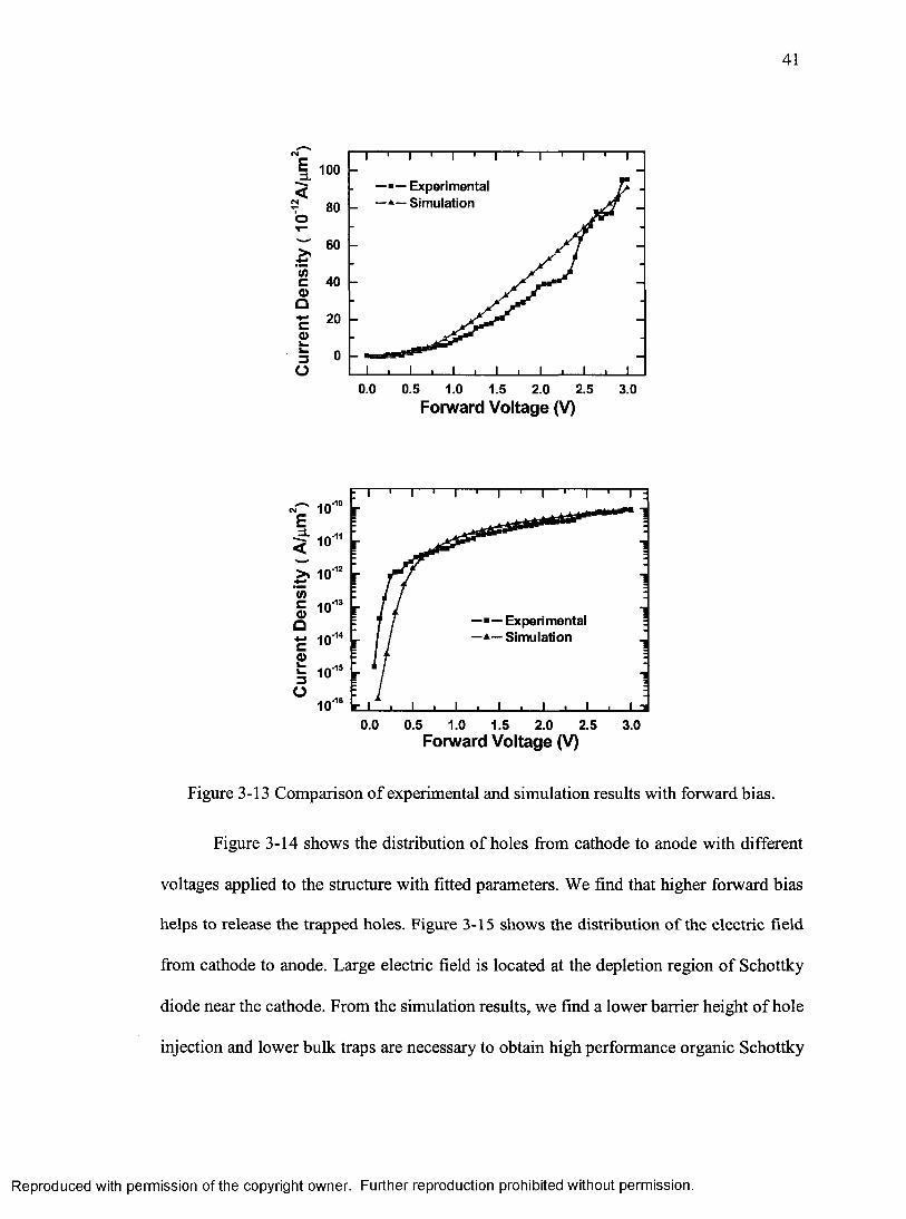
41
E 100
b80
>-4-.*
60
c0)Q
40
4 -4c0)L _
20
L -
3o
0
1 ------ 1------ 1------ 1------ 1------ 1------ 1------ r-------1------ 1------ 1------ 1------ r
-■— ExperimentalSimulation
0.0 0.5 1.0 1.5 2.0 2.5 3.0Forward Voltage (V)
1-10
,-11
,-12
(/},-13c
0)Qc£
—■ — Experimental — *■— Simulation,-14
,-15
3o,-16
0.0 0.5 1.0 1.5 2.0 2.5 3.0Forward Voltage (V)
Figure 3-13 Comparison o f experimental and simulation results with forward bias.
Figure 3-14 shows the distribution o f holes from cathode to anode with different
voltages applied to the structure with fitted parameters. We find that higher forward bias
helps to release the trapped holes. Figure 3-15 shows the distribution o f the electric field
from cathode to anode. Large electric field is located at the depletion region o f Schottky
diode near the cathode. From the simulation results, we find a lower barrier height o f hole
injection and lower bulk traps are necessary to obtain high performance organic Schottky
Reproduced with permission of the copyright owner. Further reproduction prohibited without permission.
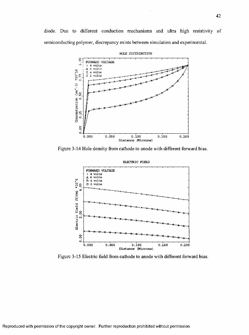
42
diode. Due to different conduction mechanisms and ultra high resistivity of
semiconducting polymer, discrepancy exists between simulation and experimental.
HOLE DISTRIBUTION
O-fFORWARD VOLTAGE + 8 v o l t s 6, S v o l t s O 4 v o l ts □ 2 v o l ts<
S* oro(<
o
0 .0 0 0 0 ,0 5 0 0 .1 0 0 0 .2 0 00 .1 5 0D is t a n c e (M ic ro n s)
Figure 3-14 Hole density from cathode to anode with different forward bias.
EISCTRIC FIELD
POGWAPSD VDLTfifiE + 8 volts A 6 volts O 4 volts □ 2 volts
r3 o
01•H
Ou
o0 .0 0 0 0 .0 5 0 0 . 1 0 0 0 .1 5 0 0 .2 0 0
D i s t a n c e (M ic ro n s)
Figure 3-15 Electric field from cathode to anode with different forward bias.
Reproduced with permission of the copyright owner. Further reproduction prohibited without permission.
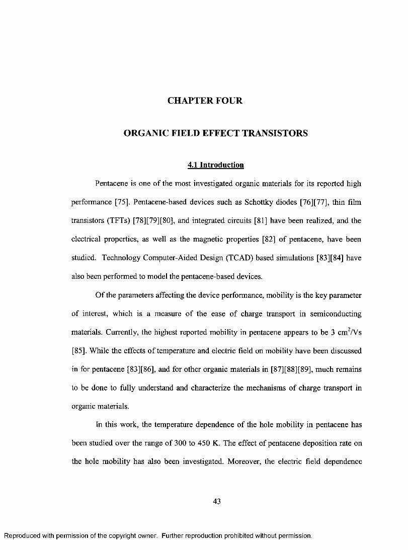
CHAPTER FOUR
ORGANIC FIELD EFFECT TRANSISTORS
4.1 Introduction
Pentacene is one o f the most investigated organic materials for its reported high
performance [75], Pentacene-based devices such as Schottky diodes [76][77], thin film
transistors (TFTs) [78][79][80], and integrated circuits [81] have been realized, and the
electrical properties, as well as the magnetic properties [82] o f pentacene, have been
studied. Technology Computer-Aided Design (TCAD) based simulations [83][84] have
also been performed to model the pentacene-based devices.
O f the parameters affecting the device performance, mobility is the key parameter
o f interest, which is a measure o f the ease o f charge transport in semiconducting
materials. Currently, the highest reported mobility in pentacene appears to be 3 cm^A^s
[85]. While the effects o f temperature and electric field on mobility have been discussed
in for pentacene [83][86], and for other organic materials in [87][88][89], much remains
to be done to fully imderstand and characterize the mechanisms o f charge transport in
organic materials.
In this work, the temperature dependence o f the hole mobility in pentacene has
been studied over the range o f 300 to 450 K. The effect of pentacene deposition rate on
the hole mobility has also been investigated. Moreover, the electric field dependence
43
Reproduced with permission of the copyright owner. Further reproduction prohibited without permission.
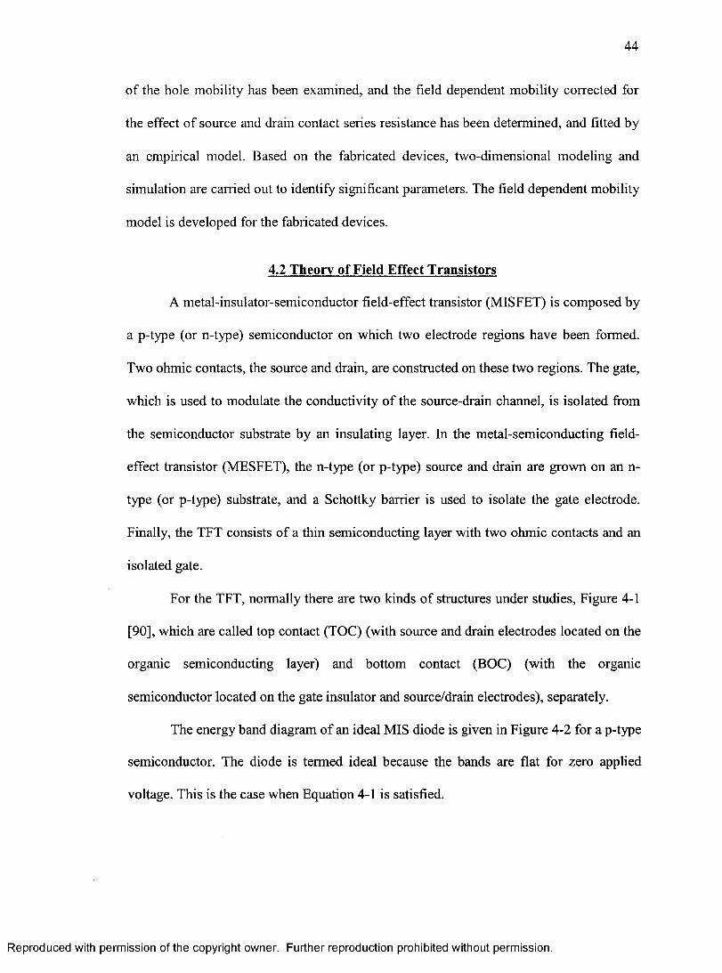
44
of the hole mobility has been examined, and the field dependent mobility corrected for
the effect o f source and drain contact series resistance has been determined, and fitted by
an empirical model. Based on the fabricated devices, two-dimensional modeling and
simulation are carried out to identify significant parameters. The field dependent mobility
model is developed for the fabricated devices.
4.2 Theory of Field Effect Transistors
A metal-insulator-semiconductor field-effect transistor (MISFET) is composed by
a p-type (or n-type) semiconductor on which two electrode regions have been formed.
Two ohmic contacts, the source and drain, are constructed on these two regions. The gate,
which is used to modulate the conductivity o f the source-drain chaimel, is isolated from
the semiconductor substrate by an insulating layer. In the metal-semiconducting field-
effect transistor (MESFET), the n-type (or p-type) source and drain are grown on an n-
type (or p-type) substrate, and a Schottky barrier is used to isolate the gate electrode.
Finally, the TFT consists of a thin semiconducting layer with two ohmic contacts and an
isolated gate.
For the TFT, normally there are two kinds o f structures under studies. Figure 4-1
[90], which are called top contact (TOC) (with source and drain electrodes located on the
organic semiconducting layer) and bottom contact (BOG) (with the organic
semiconductor located on the gate insulator and source/drain electrodes), separately.
The energy band diagram of an ideal MIS diode is given in Figure 4-2 for a p-type
semiconductor. The diode is termed ideal because the bands are flat for zero applied
voltage. This is the case when Equation 4-1 is satisfied.
Reproduced with permission of the copyright owner. Further reproduction prohibited without permission.
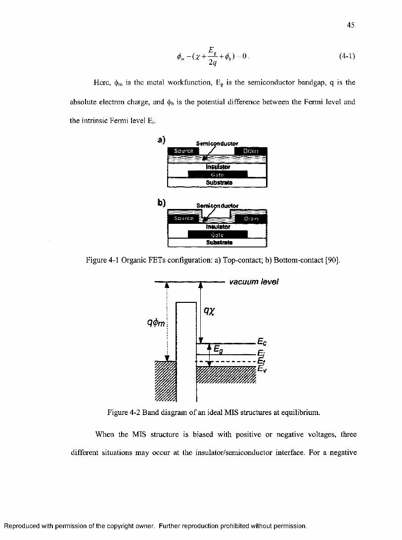
4 - ( ^ + + ^(,) = 0 2q
45
(4-1)
Here, (j)m is the metal workfunction. Eg is the semiconductor bandgap, q is the
absolute electron charge, and (|)b is the potential difference between the Fermi level and
the intrinsic Fermi level Ei.
SA iieMdyctfrr
Figure 4-1 Organic FETs configuration; a) Top-contact; b) Bottom-contact [90].
q<ffm
vacuum level
q x
Figure 4-2 Band diagram of an ideal MIS structures at equilibrium.
When the MIS structure is biased with positive or negative voltages, three
different situations may occur at the insulator/semiconductor interface. For a negative
Reproduced with permission of the copyright owner. Further reproduction prohibited without permission.
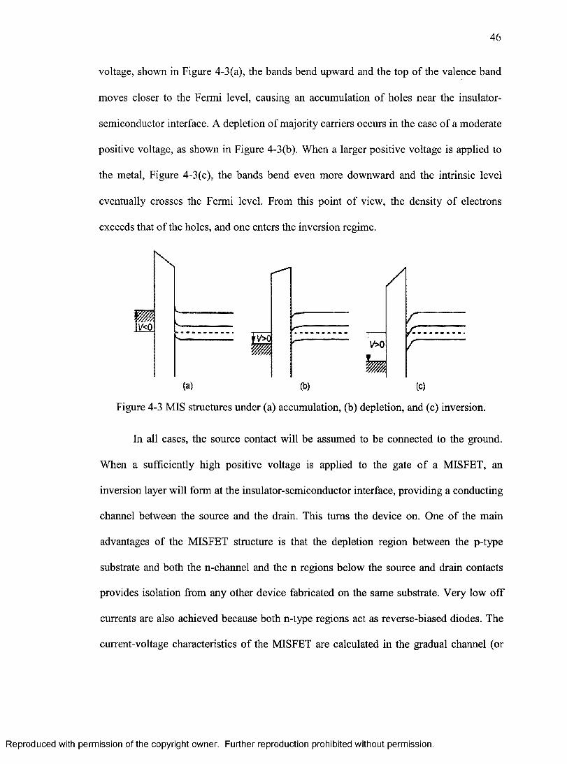
46
voltage, shown in Figure 4-3(a), the bands bend upward and the top o f the valence band
moves closer to the Fermi level, causing an accumulation o f holes near the insulator-
semiconductor interface. A depletion of majority carriers occurs in the case o f a moderate
positive voltage, as shown in Figure 4-3(b). When a larger positive voltage is applied to
the metal. Figure 4-3(c), the bands bend even more downward and the intrinsic level
eventually crosses the Fermi level. From this point o f view, the density o f electrons
exceeds that o f the holes, and one enters the inversion regime.
V'>0
(a) (b) (c)
Figure 4-3 MIS structures under (a) accumulation, (b) depletion, and (c) inversion.
In all cases, the source contact will be assumed to be connected to the ground.
When a sufficiently high positive voltage is applied to the gate o f a MISFET, an
inversion layer will form at the insulator-semiconductor interface, providing a conducting
channel between the source and the drain. This turns the device on. One o f the main
advantages o f the MISFET structure is that the depletion region between the p-type
substrate and both the n-channel and the n regions below the source and drain contacts
provides isolation from any other device fabricated on the same substrate. Very low off
currents are also achieved because both n-type regions act as reverse-biased diodes. The
current-voltage characteristics o f the MISFET are calculated in the gradual channel (or
Reproduced with permission of the copyright owner. Further reproduction prohibited without permission.
47
Shockley) approximation [97] based on the assumption that the electric charge density
related to a variation o f the electric field along the channel is much smaller than that
related to a variation across the chaimel, namely |dFx/dx| « |dFy/dy|, where F is the
electric field, and x and y are the directions parallel and perpendicular to the insulator-
semiconductor interface, respectively. This condition is generally fulfilled when the
channel length L is much larger than the insulator thickness di. If we assume in addition
that the charge mobility /x is constant, the drain current Ids is related to the source-drain
voltage Vds and the source-gate voltage Vgs through Equation 4-2 [97],
-2 ^ , - ( 2 ^ ,r " ) ) (4-2)
Here, W is the channel width, Ci is the insulator capacitance (per unit area), eg is
the semiconductor permittivity, and Na is the doping level o f the p-type substrate.
Equation 4-2 predicts that the drain current first increases linearly with the drain voltage
for a given gate voltage known as linear regime, then gradually levels off to a constant
value known as saturation regime. It also predicts that the drain current increases when
the gate voltage increases. For a small Vds, Equation 4-2 reduces to Equation 4-3, where
the threshold voltage Vth corresponds to the onset o f the strong inversion regime, and is
given by Equation 4-4,
(4-3)
(4.4)
where Vfb is the flat-band voltage.
Reproduced with permission of the copyright owner. Further reproduction prohibited without permission.
48
Two important technological parameters are the channel conductance gds and the
transconductance gm, whieh are represented by Equation 4-5 and Equation 4-6 in the
linear regime, respectively. In the saturation regime, the drain current and
transconductanee are given by Equation 4-7 and Equation 4-8, respectively.
S dsdl ds
dV,
S„
ds
dl ds
dV.gs Vds-const
W
JVI d s , s . = - I ^ C , i V ^ - V „ f
(4-5)
(4-6)
(4-7)
(4-8)
The concept o f the thin film transistor (TFT) was first introduced by Weimer in
1962 [91]. This structure is well adapted to low conductivity materials, and is now
currently used in amorphous silicon transistors [92]. As seen in Figure 4-1, the source and
drain electrodes form ohmic contacts directly to the conducting channel. Unlike both the
structures described above, there is no depletion region to isolate the device from the
substrate. Low off-state current is only guaranteed by the low conductivity o f the
semiconductor. A second crucial difference to the traditional MISFET is that, although
the TFT is an insulated gate device, it operates in the accumulation regime and not in the
inversion regime. For this reason, care has to be taken when transferring the equations o f
the drain current from the MISFET to the TFT. In fact, the absence o f a depletion region
leads to a simplification o f Equation 4-2, which can now be written as Equation 4-9.
JV V= - / / C , ( F (4-9)
Reproduced with permission of the copyright owner. Further reproduction prohibited without permission.
49
Here, the threshold voltage is the gate voltage for which the channel conductance
is equal to that o f the whole semiconducting layer. It is given by Equation 4-10 [50],
where N is the density o f doping centers. Equation 4-10 assumes that all doping centers
are ionized when the concentration o f free carriers is much lower than that o f trapped
carriers, where Nt is the trap density:
JlkTe.SQN.(4-10)
In the saturation regime, the current is given by Equation 4-7. It must be kept in
mind that this equation was derived under assumptions that are not always fulfilled in
organic semiconductors, particularly that o f a constant mobility.
4.3 N-channel Field Effect Transistors
4.3.1 Introduction
Compared to the p-type organic materials, n-type organic materials have much
lower mobility, and are more sensitive to the environments due to the transport
mechanism for organic materials. Among several n-type materials, NTCDA is more
promising due to its high mobility o f 0.06 cm W s [93] and investigated stabilities [94].
In this section, the depletion-mode n-channel OFETs based on NTCDA are
fabricated and characterized. From the discussions and analyses o f charge transport and
energy bands, the mechanism and function o f this OFET are introduced and demonstrated.
The mobility o f 0.016 cm^A^s was obtained from Ids - Vds data in the saturation region at
Vgs = 0 V. The threshold voltage is -32 V (from Ids -V gs data in the linear region by the
linear extrapolation method (Vds 20 V)), the cut off current is 1.76 nA, and the on/off
ratio at saturation region (Vds = 60 V) is 2.25 x 10 . The environmental effects
Reproduced with permission of the copyright owner. Further reproduction prohibited without permission.
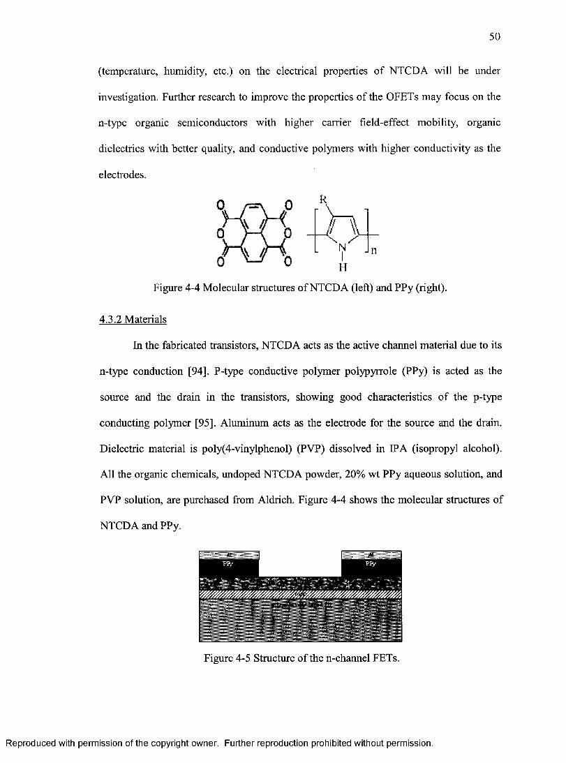
50
(temperature, humidity, etc.) on the electrical properties o f NTCDA will be under
investigation. Further research to improve the properties of the OFETs may focus on the
n-type organic semiconductors with higher carrier field-effect mobility, organic
dielectrics with better quality, and conductive polymers with higher conductivity as the
electrodes.
R
NIII
Figure 4-4 Molecular structures o f NTCDA (left) and PPy (right).
4.3.2 Materials
In the fabricated transistors, NTCDA acts as the active chaimel material due to its
n-type conduction [94]. P-type conductive polymer polypyrrole (PPy) is acted as the
source and the drain in the transistors, showing good characteristics o f the p-type
conducting polymer [95]. Aluminum acts as the electrode for the source and the drain.
Dielectric material is poly(4-vinylphenol) (PVP) dissolved in IPA (isopropyl alcohol).
All the organic chemicals, undoped NTCDA powder, 20% wt PPy aqueous solution, and
PVP solution, are purchased from Aldrich. Figure 4-4 shows the molecular structures of
NTCDA and PPy.
Figure 4-5 Structure o f the n-channel FETs.
Reproduced with permission of the copyright owner. Further reproduction prohibited without permission.
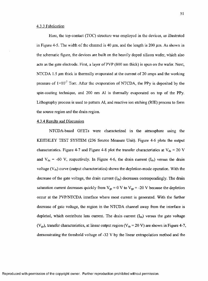
51
4.3.3 Fabrication
Here, the top-contact (TOC) structure was employed in the devices, as illustrated
in Figure 4-5. The width o f the channel is 40 jum, and the length is 200 /xm. As shown in
the schematic figure, the devices are built on the heavily doped silicon wafer, which also
acts as the gate electrode. First, a layer o f PVP (800 nm thick) is spun on the wafer. Next,
NTCDA 1.5 jum thick is thermally evaporated at the current o f 20 amps and the working
npressure o f 1x10' Torr. After the evaporation o f NTCDA, the PPy is deposited by the
spin-coating technique, and 200 nm A1 is thermally evaporated on top of the PPy.
Lithography process is used to pattern Al, and reactive ion etching (RIE) process to form
the source region and the drain region.
4.3.4 Results and Discussion
NTCDA-based OFETs were characterized in the atmosphere using the
KEITHLEY TEST SYSTEM (236 Source Measure Unit). Figure 4-6 plots the output
characteristics. Figure 4-7 and Figure 4-8 plot the transfer characteristics at Yds = 20 V
and Yds = -60 Y, respectively. In Figure 4-6, the drain current (Us) versus the drain
voltage (Yds) curve (output characteristics) shows the depletion-mode operation. With the
decrease o f the gate voltage, the drain current (Us) decreases correspondingly. The drain
saturation current decreases quickly from Ygs = 0 Y to Ygs = -20 Y because the depletion
occur at the PYP/NTCDA interface where most current is generated. With the further
decrease o f gate voltage, the region in the NTCDA channel away from the interface is
depleted, which contribute less current. The drain current (Ids) versus the gate voltage
(Ygs), transfer characteristics, at linear output region (Yds = 20 Y) are shown in Figure 4-7,
demonstrating the threshold voltage o f -32 Y by the linear extrapolation method and the
Reproduced with permission of the copyright owner. Further reproduction prohibited without permission.
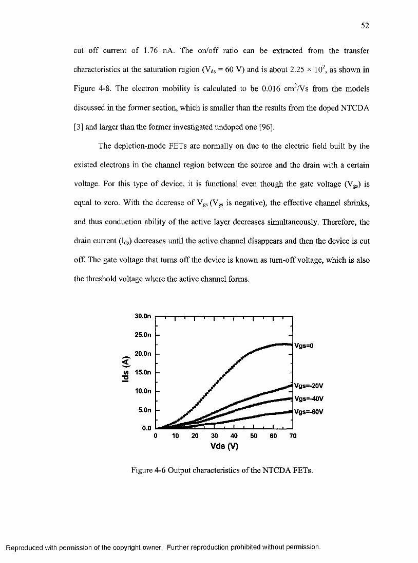
52
cut off current o f 1.76 nA. The on/off ratio can be extracted from the transfer
characteristics at the saturation region (Vds = 60 V) and is about 2.25 x 10^, as shown in
Figure 4-8. The electron mobility is calculated to be 0.016 cm^/Vs from the models
discussed in the former section, which is smaller than the results from the doped NTCDA
[3] and larger than the former investigated undoped one [96].
The depletion-mode FETs are normally on due to the electric field built by the
existed electrons in the channel region between the source and the drain with a certain
voltage. For this type o f device, it is functional even though the gate voltage (Vgs) is
equal to zero. With the decrease o f Vgs (Vgs is negative), the effective channel shrinks,
and thus conduction ability o f the active layer decreases simultaneously. Therefore, the
drain current (Ids) decreases until the active channel disappears and then the device is cut
off. The gate voltage that turns off the device is known as tum -off voltage, which is also
the threshold voltage where the active chatmel forms.
30.0n
25.0n
Vgs=020.0n
<tn 15.0n ■D
Vgs=-20V
Vgs=-40V
Vgs=-60V
10.0n
S.On
0.00 10 20 30 40 50 60 70
Vds(V)
Figure 4-6 Output characteristics o f the NTCDA FETs.
Reproduced with permission of the copyright owner. Further reproduction prohibited without permission.
53
Generally, the analjhic models Equations 4-7 and 4-9 are employed to describe
the behavior of organic transistors [97], transfer and output characteristics. They are
rewritten here.
WC: ... ^2
Ids ^ —7 ^ l iVgs - Kh — ^ ) K s (Linear - region) (4-11)
JVCIds = ! (Vgs - V ,h f (Saturation - region) (4-1 2 )
From the energy-hand theory and the interfacial effect, the more insight o f the
OFET can be analyzed. Table 4-1 [98] [99] gives the parameters (work frmction $ , energy
gap Eg, and Fermi level or effective Fermi level Ef) for the materials used in the
fabricated OFETs. At the gate voltage o f zero, the channel is completely open, and the
electrons can be injected into the channel without barriers. The higher the drain current
(Vds), the more electrons injected. The largest drain current is obtained when the channel
becomes saturation. When the gate voltage is decreased, the conduction band o f heavily
doped silicon will increase; thus, the positive charges are accumulated in the interface
and negative charges are partly depleted in the channel. Moreover, the capability of
electron-activated n-type channel is weakened. If the gate voltage is below the threshold
voltage, the chaimel will be turned off, and the drain current will not be formed even
collected with the high drain voltage.
Another issue is that the conducting channel is inside the bulk o f the active layer
for the depletion-mode operated devices compared to the channel at the interfaee between
the dielectric layer and the active layer for the accumulation-mode operated devices,
especially for the TOC structure.
Reproduced with permission of the copyright owner. Further reproduction prohibited without permission.
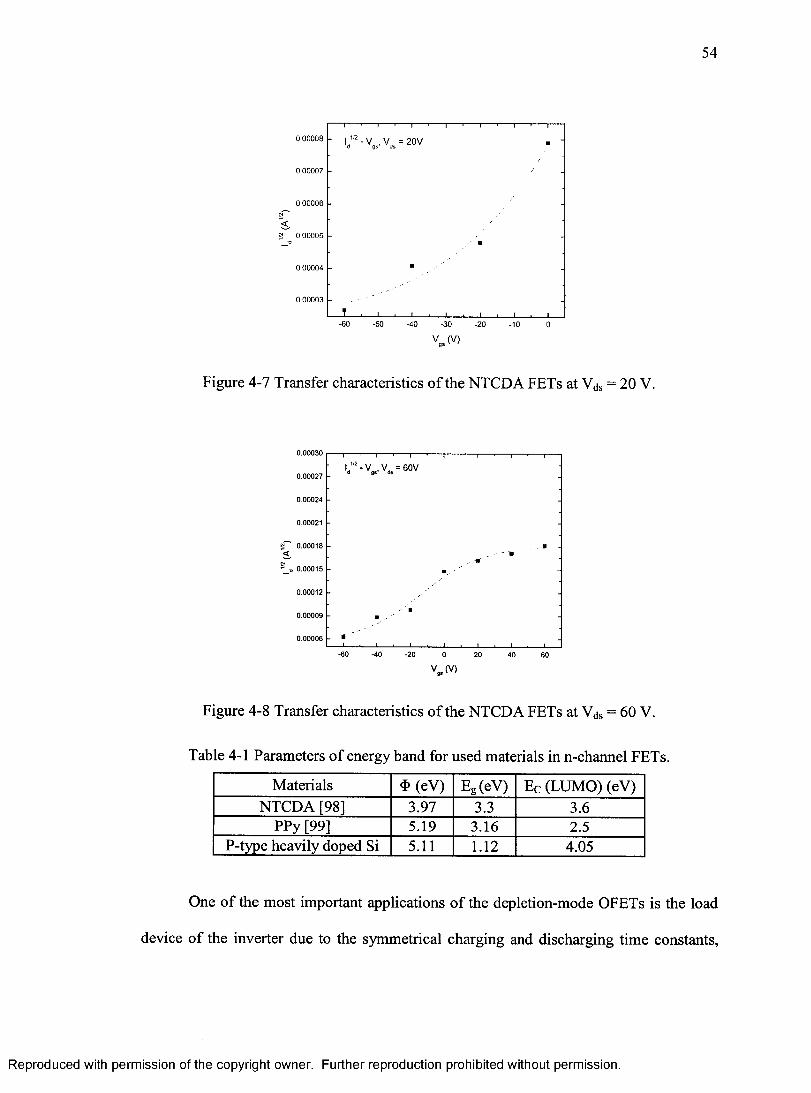
54
0.00008 - V , V = 20Vd gs ds
0.00007
0.00006
0.00005
0.00004
0.00003
-60 -50 -40 -30 -20 -10 0
V.(V)
Figure 4-7 Transfer characteristics o f the NTCDA FETs at Vds = 20 V.
0.00030
,v , =60Vd g s’ ds0.00027
0.00024
0.00021
0.00018
0.00015
0.00012
0.00009
0.00006
-60 -40 -20 0 20 40 60
V.(V)
Figure 4-8 Transfer characteristics o f the NTCDA FETs at Yds = 60 V.
Table 4-1 Parameters o f energy band for used materials in n-channel FETs.
Materials $ (eV) Eg(eV) Ec (LUMO) (eV)NTCDA [981 3.97 3.3 3.6
PPy [99] 5.19 3.16 2.5P-type heavily doped Si 5.11 1 . 1 2 4.05
One of the most important applications o f the depletion-mode OFETs is the load
device o f the inverter due to the symmetrical charging and discharging time constants,
Reproduced with permission of the copyright owner. Further reproduction prohibited without permission.
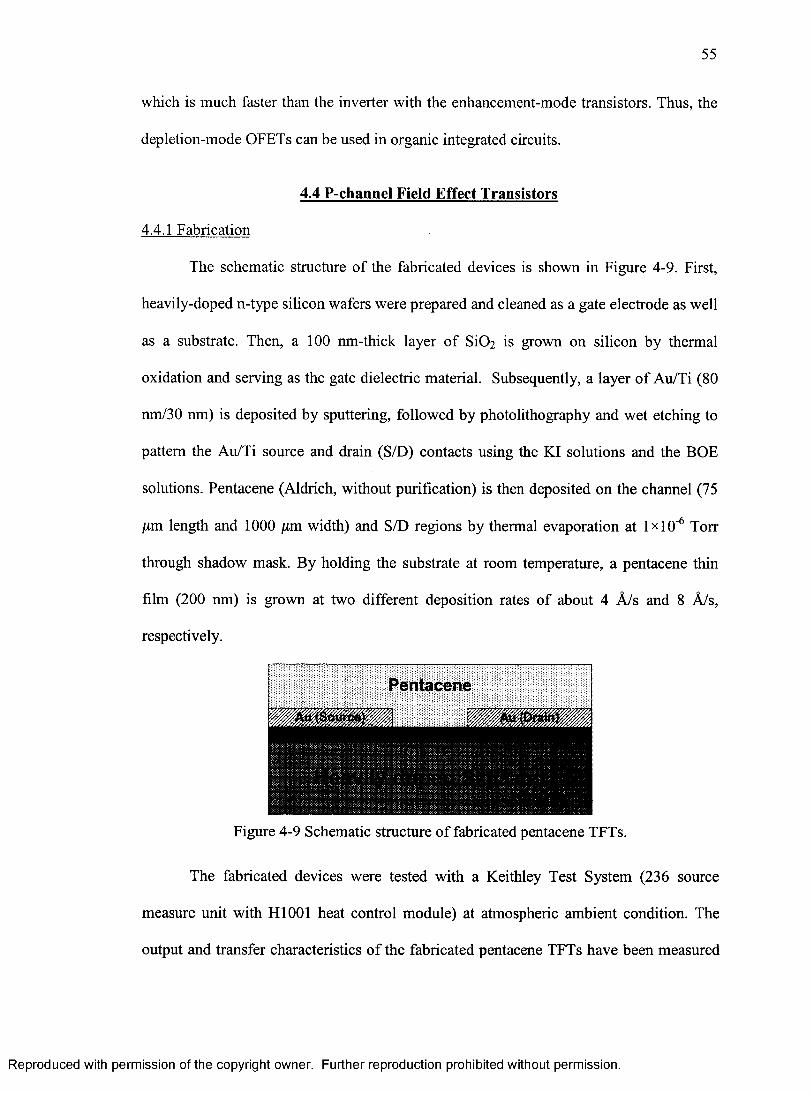
55
which is much faster than the inverter with the enhancement-mode transistors. Thus, the
depletion-mode OFETs can be used in organic integrated circuits.
4.4 P-channel Field Effect Transistors
4.4.1 Fabrication
The schematic structure o f the fabricated devices is shown in Figure 4-9. First,
heavily-doped n-type silicon wafers were prepared and cleaned as a gate electrode as well
as a substrate. Then, a 100 nm-thick layer o f Si0 2 is grown on silicon by thermal
oxidation and serving as the gate dielectric material. Subsequently, a layer o f Au/Ti (80
nm/30 nm) is deposited by sputtering, followed by photolithography and wet etching to
pattem the Au/Ti source and drain (S/D) contacts using the KI solutions and the BOE
solutions. Pentacene (Aldrich, without purification) is then deposited on the channel (75
/xm length and 1000 |xm width) and S/D regions by thermal evaporation at IxlO'^ Torr
through shadow mask. By holding the substrate at room temperature, a pentacene thin
film ( 2 0 0 nm) is grown at two different deposition rates o f about 4 A/s and 8 A/s,
respectively.
Figure 4-9 Schematic structure o f fabricated pentacene TFTs.
The fabricated devices were tested with a Keithley Test System (236 source
measure unit with H I001 heat control module) at atmospheric ambient condition. The
output and transfer characteristics o f the fabricated pentacene TFTs have been measured
Reproduced with permission of the copyright owner. Further reproduction prohibited without permission.
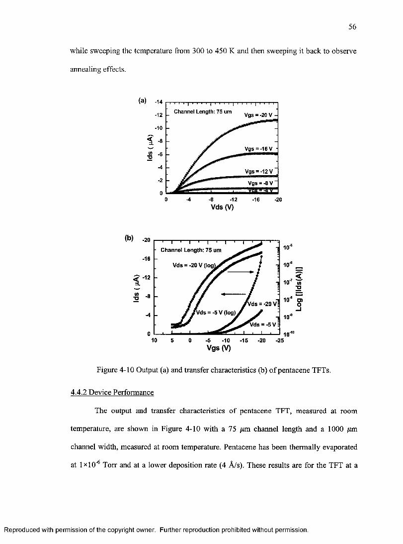
56
while sweeping the temperature from 300 to 450 K and then sweeping it back to observe
annealing effects.
(a)Channel Length: 75 um
-12 Vgs = -20 V -
-10
1Vgs = -16 V -
(A■O
Vgs = -12 V
Vgs = -8 V “
0 -4 -8 -12 -16 -20V d s (V )
-20
- Channel Length: 75 um-16
Vds = -20 V (log’
-12
-8
'ds = -2 0 VVds = -5 V (log)-4
Vds = -5V,-100
10 05 -5 -10 -15 -20 -25V g s ( V )
Figure 4-10 Output (a) and transfer characteristics (b) o f pentacene TFTs.
4.4.2 Device Performance
The output and transfer characteristics o f pentacene TFT, measured at room
temperature, are shown in Figure 4-10 with a 75 /xm channel length and a 1000 /xm
chaimel width, measured at room temperature. Pentacene has been thermally evaporated
at 1x10'^ Torr and at a lower deposition rate (4 A/s). These results are for the TFT at a
Reproduced with permission of the copyright owner. Further reproduction prohibited without permission.
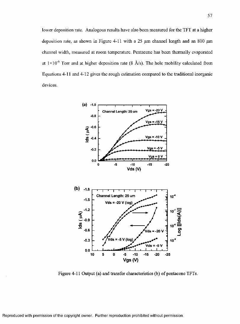
57
lower deposition rate. Analogous results have also been measured for the TFT at a higher
deposition rate, as shown in Figure 4-11 with a 25 [xm channel length and an 800 jum
channel width, measured at room temperature. Pentacene has been thermally evaporated
at 1 x 1 0 ' Torr and at higher deposition rate ( 8 A/s). The hole mobility calculated from
Equations 4-11 and 4-12 gives the rough estimation compared to the traditional inorganic
devices.
■1.0
Vgs = - 2 0 V -Channel Length: 25 um- 0.8
Vgs = -1Sy -- 0.6
Vgs = -10 V _« -0.4
- 0.2
Vgs = OV •0.0
-5 -10 -15Vds(V)
-20
1 0
Channel Length: 25 um
Vds = -20 V (log) .-1.5
- 1.2
1-0.9
- 0.6 Vds = -20 V
Vds = -5 V (log)-0.3Vds = -5 V
0.0
1 0 -
10’ g(0
2
io-* = O)o
1 0 -
-5 -10 -15 -20 -25
Vgs (V)
Figure 4-11 Output (a) and transfer characteristics (b) o f pentacene TFTs.
Reproduced with permission of the copyright owner. Further reproduction prohibited without permission.
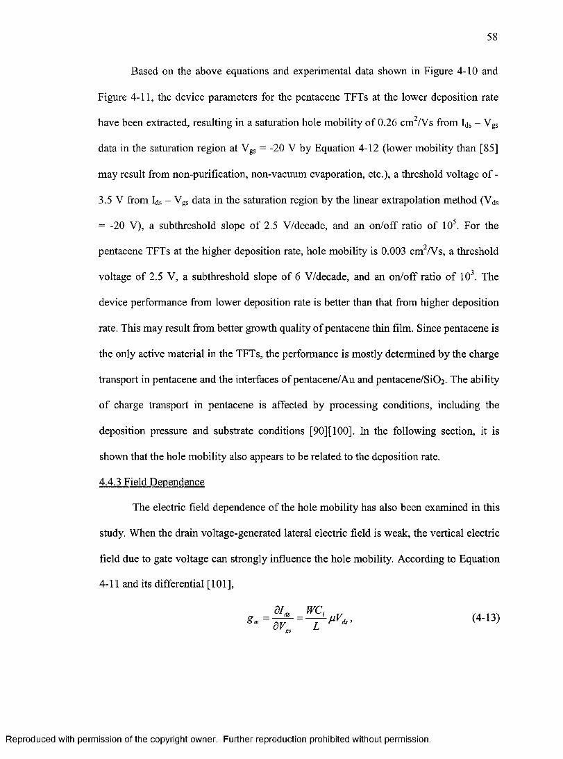
58
Based on the above equations and experimental data shown in Figure 4-10 and
Figure 4-11, the device parameters for the pentacene TFTs at the lower deposition rate
have been extracted, resulting in a saturation hole mobility o f 0.26 cm /Vs from Ids ~ Vgs
data in the saturation region at Vgs = -20 V by Equation 4-12 (lower mobility than [85]
may result from non-purification, non-vacuum evaporation, etc.), a threshold voltage o f -
3.5 V from Ids - Vgs data in the saturation region by the linear extrapolation method (Vds
= -20 V), a subthreshold slope o f 2.5 V/decade, and an on/off ratio o f 10 . For the
pentacene TFTs at the higher deposition rate, hole mobility is 0.003 cm^/Vs, a threshold
voltage o f 2.5 V, a subthreshold slope o f 6 V/decade, and an on/off ratio o f 10^. The
device performance from lower deposition rate is better than that from higher deposition
rate. This may result from better growth quality o f pentacene thin film. Since pentacene is
the only active material in the TFTs, the performance is mostly determined by the charge
transport in pentacene and the interfaces o f pentacene/Au and pentacene/Si0 2 . The ability
o f charge transport in pentacene is affected by processing conditions, including the
deposition pressure and substrate conditions [90][100]. In the following section, it is
shown that the hole mobility also appears to be related to the deposition rate.
4.4.3 Field Dependence
The electric field dependence o f the hole mobility has also been examined in this
study. When the drain voltage-generated lateral electric field is weak, the vertical electric
field due to gate voltage can strongly influence the hole mobility. According to Equation
4-11 and its differential [101],
dl WC= (4-13)
gs
Reproduced with permission of the copyright owner. Further reproduction prohibited without permission.
59
where gm is the transconductanee. Using the above equation and experimental data, the
field dependence o f mobility can be determined. Figure 4-12 shows the field dependent
hole mobility in pentacene TFTs at room temperature and Vds = -5 V. The two sets o f
results presented are for TFTs fabricated at lower and higher deposition rates,
respectively. In both cases, the mobility is noticeably increased by the increase in electric
field at higher gate voltages, while, as observed earlier, the pentacene deposition rate also
plays a major role in influencing mobility. The breakdown of the device occurs at a gate
voltage o f -90 V and a drain voltage of -105 V, which is high enough for a FET.
Unlike inorganic semiconductors, pentacene shows an increase in mobility with
an increase in the gate voltage, as shown in Figure 4-12. This phenomenon is also
reported in [88][102] for polycrystalline sexithiophene (6 T). This gate-voltage dependent
mobility is attributed to the trapping o f charge carriers by the interfacial and bulk traps at
lower values o f the gate voltage [103]. As the gate voltage increases and more traps are
filled, additional charge carriers move more freely through the channel, resulting in an
increase in mobility.
0.18 0.010
Vds = -5 V0.15
0.12
0.008 ^
Lower deposition rate0.006
0.090.004 ^
0.06
0.002 S0.03Higher deposition rate
0.00 0.0000 -4 -8 -16-12 -20
V g s (V )
Figure 4-12 Gate voltage dependent mobility in pentacene TFTs at room temperature.
Reproduced with permission of the copyright owner. Further reproduction prohibited without permission.
60
4.5 Temperature Dependence of Mobility
Temperature and electric field dependence o f the hole mobility in pentacene thin
film transistors has been studied. Mobility is the key device parameter affecting
performance in TFTs. The extracted plot o f the hole mobility (from Ids - Vgs data in the
linear or saturation region by Equations 4-11 and 4-12) as a function o f temperature is
shown in Figure 4-13 at Yds = -20 V (saturation region) and Yds = -5 Y (linear region) for
different gate voltages for pentacene TFTs at lower deposition rate (4 A/s). It is found
that over the temperature range of 300 to 450 K, the hole mobility increases to a peak
value and then decreases to very low values. Previous experiments and analyses have
indicated that thermally activated hopping transport occurs in some organic materials
below room temperature [87][104]. Here, the hole mobility increases with temperature,
displaying the Arrhenius behavior. But above room temperature, as the temperature is
increased, the mobility in pentacene eventually decreases. This is attributed to the higher
carrier scattering occurring at more elevated temperatures. Scattering phenomena
increasingly dominate the behavior o f transistors and thus determine the performance of
the devices with the increase in temperature. Moreover, at higher temperatures,
eventually pentacene ceases acting as an active material.
As illustrated in Figure 4-14, by fabricating the TFTs with higher pentacene
deposition rate, a similar type o f result and behavior is obtained at Yds = -30 Y (saturation
region) and Vds = -5 V (linear region) for different gate voltages for pentacene TFTs at a
higher deposition rate (8 A/s) as in Figure 4-13, except that there is over twenty times a
reduction in the extracted hole mobility values. This is attributed to the change in the
Reproduced with permission of the copyright owner. Further reproduction prohibited without permission.
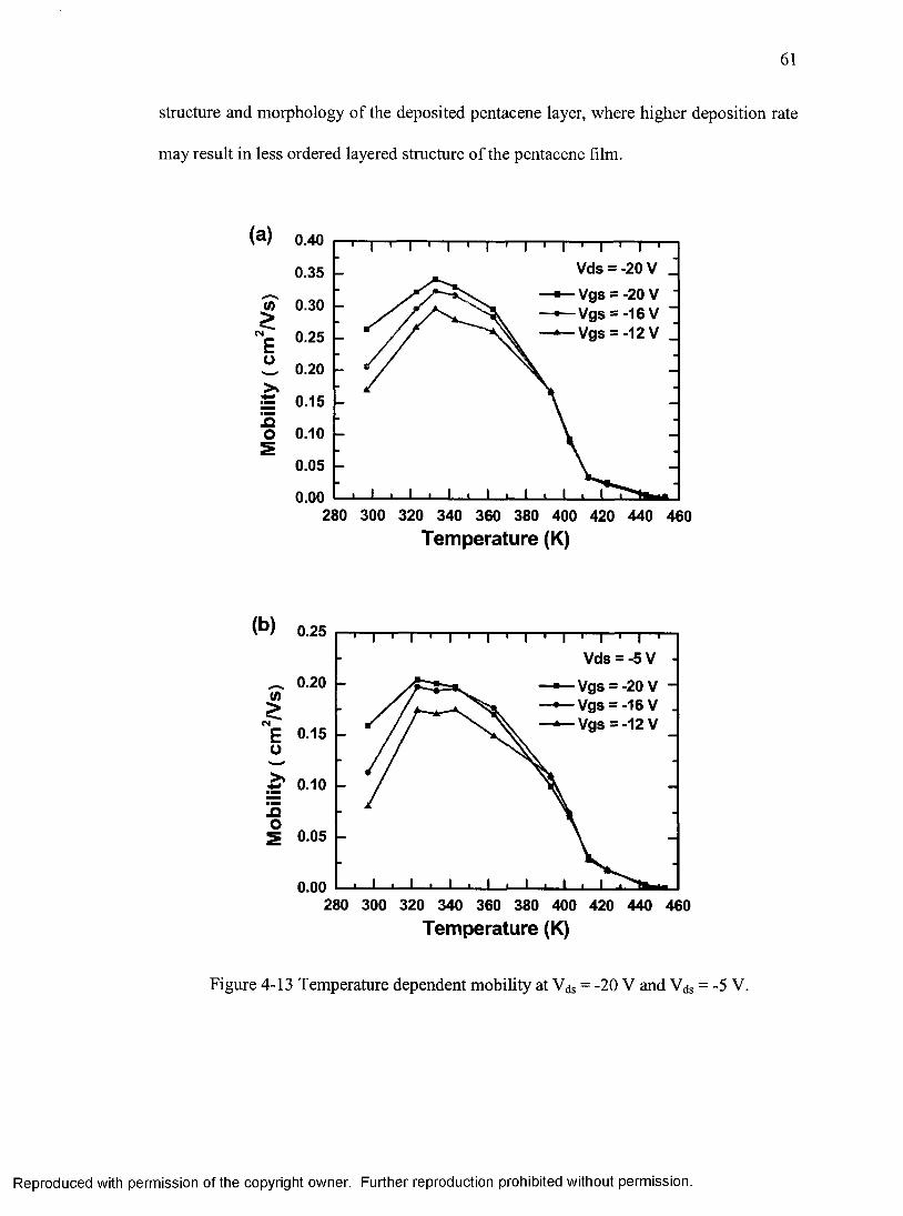
61
structure and morphology o f the deposited pentacene layer, where higher deposition rate
may result in less ordered layered structure o f the pentacene fdm.
(a)
(A
CM
Eo
o
0.40Vds = -20 V _Vgs = -20 V ■ Vgs = -16 V “ Vgs = -12 V J
0.35
0.30
0.25
0.20
0.15
0.10
0.05
0.00280 300 320 340 360 380 400 420 440 460
Temperature (K)
(1 ) 0.25Vds = -5 V
Vgs = -20 V Vgs = -16 V Vgs = -12 V
^ 0.20 (A
. 5E 0.15 o
0.00280 300 320 340 360 380 400 420 440 460
Temperature (K)
Figure 4-13 Temperature dependent mobility at Vds - -20 V and Yds = -5 V.
Reproduced with permission of the copyright owner. Further reproduction prohibited without permission.
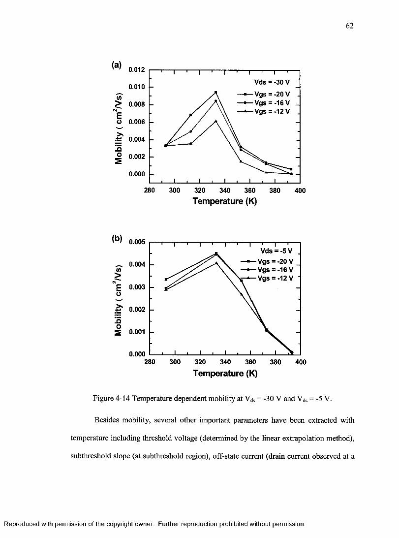
62
(a) 0.012
0.010 hV>^ 0.008
CM
£O 0.006
0.004 I-!5O 0.002 -
0.000 -
1 ' rVds = -30 V
— Vgs = -20V ^ V g s = -16V -^Vgs = -12 V
280 300 320 340 360 380 400Temperature (K)
(b) 0.005
^ 0.004 (0
0.003o^ 0.002 I-
!os 0.001
0.000
Vds = -5 VVgs = -20 V Vgs = -16V Vgs = -12 V
- I 1 I I I I I I I I L
280 300 320 340 360 380 400Temperature (K)
Figure 4-14 Temperature dependent mobility at Vds = -30 V and Yds = -5 V.
Besides mobility, several other important parameters have been extracted with
temperature including threshold voltage (determined by the linear extrapolation method),
subthreshold slope (at subthreshold region), off-state current (drain current observed at a
Reproduced with permission of the copyright owner. Further reproduction prohibited without permission.
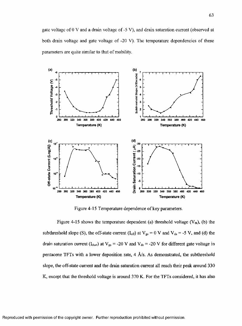
63
gate voltage o f 0 V and a drain voltage o f -5 V), and drain saturation current (observed at
both drain voltage and gate voltage o f -20 V). The temperature dependencies o f these
parameters are quite similar to that o f mobility.
■6
•5>Q>O)re •4
O -3 > ^ ■oO -2£i/iOL.£
I -
•1
0280 300 320 340 360 380 400 420 440 460
70)<0o 6 QS ' 5 o a oV) 42o■S 3
2
1280 300 320 340 360 380 400 420 440 460
Temperature (K) Temperature (K)
280 300 320 340 360 380 400 420 440 460
-30
-25
-15
Q 280 300 320 340 360 380 400 420
Temperature (K)460
Temperature (K)
Figure 4-15 Temperature dependence o f key parameters.
Figure 4-15 shows the temperature dependent (a) threshold voltage (Vth), (b) the
subthreshold slope (S), the off-state current (loff) at Vgs = 0 V and Yds = -5 V, and (d) the
drain saturation current (Idsat) at Vgs = -20 V and Vds = -20 V for different gate voltage in
pentacene TFTs with a lower deposition rate, 4 A/s. As demonstrated, the subthreshold
slope, the off-state current and the drain saturation current all reach their peak around 330
K, except that the threshold voltage is around 370 K. For the TFTs considered, it has also
Reproduced with permission of the copyright owner. Further reproduction prohibited without permission.
64
been observed that by sweeping back the temperature and re-testing the devices again,
almost the same device characteristics are measured up to a temperature of about 410 K,
demonstrating no apparent thermal annealing effects below this temperature.
4.6 Modeling and Simulation
4.6.1 Introduction
With the development o f organic microelectronics, Technology Computer-Aided
Design (TCAD) based simulations are carried out to describe the behaviors o f organic
TFTs numerically based on different emphases: The effects o f traps
[105][106][107][108], field-dependent mobility models [83][109], device structures
(bottom contact and top contact) [1 1 0 ], a variety o f channel length [1 1 1 ], electrode
contact [1 1 2 ], etc.
Since pentacene thin film are normally formed by deposition (such as
evaporation) rather than grown as a single crystal, the thin film is o f an amorphous or a
polycrystalline nature with a great number o f defects, which give rise to a continuous
distribution o f traps within the band gap [113]. The trap states exert strong effects on the
electrical behavior o f the device by trapping and holding carriers located within the
channel. At the same time, interfacial charges are also introduced during the formation of
pentacene thin film. Unlike the interface o f Si/SiOa formed by thermal oxidation, the
interface charges are significant due to the deposition process for organic/inorganic
heterostructures. The interface charges contribute to the distribution o f carriers near the
interface o f the channel/insulator, the most important region to field effect transistors. In
the following parts o f this section, we report a two-dimensional modeling and simulation
o f pentacene field effect transistors by the influence o f bulk traps and interface charges.
Reproduced with permission of the copyright owner. Further reproduction prohibited without permission.
65
Moreover, a model for field dependent mobility will be applied to the fabricated device
as demonstrated before. The TCAD tool Taurus-Device (Synopsys®) is employed to
simulate the transfer characteristics and output characteristics of the fabricated devices.
4.6.2 Models
The simulated structure of the thin film transistor is shown in Figure 4-1. Two-
dimensional simulations have been carried out using the standard drift-diffusion model
implemented in the numerical program Taurus-Dcvicc [114]. The program solves the
Poisson equation for the intrinsic potential,
fV V = -q {p - n - N - , + N ; , ) - p , (4-14)
with the ionized acceptor and donor concentrations Na' and Nd^, surface charge density
Ps, electrostatic potential (j>, and the continuity equations for the hole and electron
densities p and n,
^ = (4-15)ot q
dt q^ = — V - -U ^ = F ^ { (p ,n ,p ) (4-16)
where Un and Up represent net electron and hole recombination, respectively. From
Boltzmann transport theory, both the electron and hole current densities J„ and Jp and the
charge carrier densities in the nondegenerate case are related to the quasi-Fermi potentials
0 Fn and 0 Fp,
Jn = -<inp„'^9Fn + = qnp^E„ + q D ^ n (4-17)
Jp = -qPFp^(pFp - ^DpVp = qpPpEp - qD^Vp (4-18)
and
Reproduced with permission of the copyright owner. Further reproduction prohibited without permission.
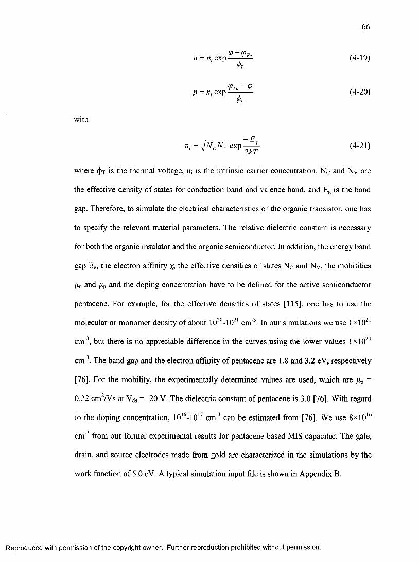
66
n = w,. exp —— (4-19)(f)j
(Pp -(Pp - exp — ------ (4-20)
<!>t
with
(4-21)
where (J)t is the thermal voltage, rii is the intrinsic carrier concentration, Nc and Ny are
the effective density o f states for conduction band and valence band, and Eg is the band
gap. Therefore, to simulate the electrical characteristics of the organic transistor, one has
to specify the relevant material parameters. The relative dielectric constant is necessary
for both the organic insulator and the organic semiconductor. In addition, the energy band
gap Eg, the electron affinity %, the effective densities o f states Nc and Ny, the mobilities
Pa and /Xp and the doping concentration have to be defined for the active semiconductor
pentacene. For example, for the effective densities o f states [115], one has to use the
molecular or monomer density o f about 1 0 - 1 0 cm' . In our simulations we use 1 x 1 0
cm'^, but there is no appreciable difference in the curves using the lower values 1 x 1 0 *
cm' . The band gap and the electron affinity o f pentacene are 1.8 and 3.2 eV, respectively
[76]. For the mobility, the experimentally determined values are used, which are /Xp =
0.22 cm^A^s at V<js = -20 V. The dielectric constant o f pentacene is 3.0 [76]. With regard
to the doping concentration, lO'^-lO'^ cm'^ can be estimated from [76]. We use 8x10*^
cm'^ from our former experimental results for pentacene-based MIS capacitor. The gate,
drain, and source electrodes made from gold are characterized in the simulations by the
work fimction o f 5.0 eV. A typical simulation input file is shown in Appendix B.
Reproduced with permission of the copyright owner. Further reproduction prohibited without permission.
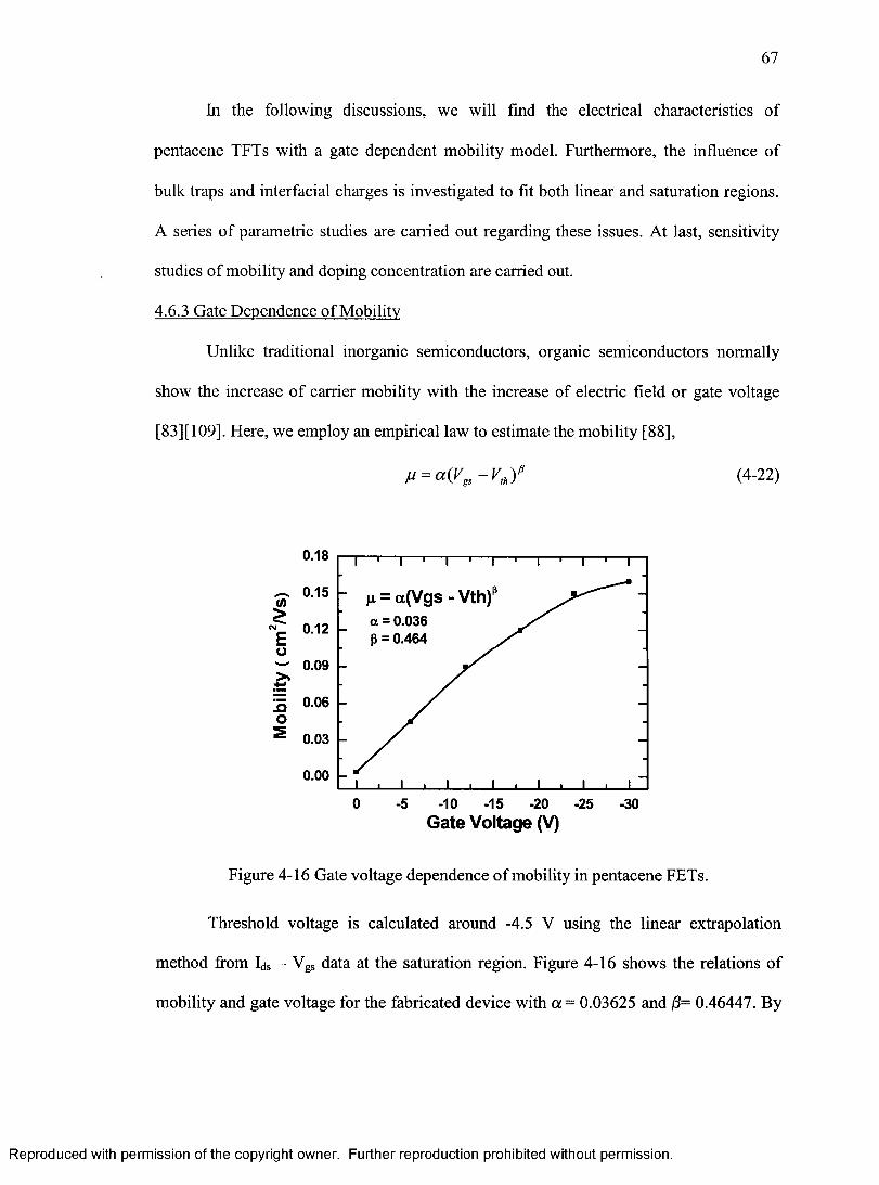
67
In the following discussions, we will find the electrical characteristics of
pentacene TFTs with a gate dependent mohility model. Furthermore, the influence of
bulk traps and interfacial charges is investigated to fit both linear and saturation regions.
A series o f parametric studies are carried out regarding these issues. At last, sensitivity
studies o f mobility and doping concentration are carried out.
4.6.3 Gate Dependence o f Mobilitv
Unlike traditional inorganic semiconductors, organic semiconductors normally
show the increase o f carrier mobility with the increase of electric field or gate voltage
[83][109]. Here, we employ an empirical law to estimate the mobility [8 8 ],
= (4-22)
(0
CMEui!5o
0.18
0.15
0.12
0.09
0.06
0.03
0.00
0 ■5 -10 -15 -20 -25 -30Gate Voltage (V)
Figure 4-16 Gate voltage dependence o f mobility in pentacene FETs.
Threshold voltage is calculated around -4.5 V using the linear extrapolation
method from Ids - Vgs data at the saturation region. Figure 4-16 shows the relations of
mobility and gate voltage for the fabricated device with a = 0.03625 and /3= 0.46447. By
Reproduced with permission of the copyright owner. Further reproduction prohibited without permission.
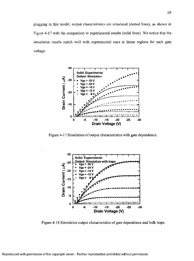
68
plugging in this model, output characteristics arc simulated (dotted lines), as shown in
Figure 4-17 with the comparison to experimental results (solid lines). We notice that the
simulation results match well with experimental ones at linear regions for each gate
voltage.
-40 - I 1- - - - - - - - - 1-- - - - - - - - 1- - - - - - - - - 1- - - - - - - - - 1- - - - - - - - - 1- - - - - - - - - 1- - - - - - - - - 1- - - - - - - - - 1-- - - - - - - - r
Solid: ExperimentalDotted: Simulation
1 -30 - ■ Vgs = -30 V-—' • Vgs = -24 Vc • i Vgs = -18 V ,0)b.L.3
-20 T Vgs = -12 V , V » Vgs= - 6 V , ^ ,
o ■x • —cn -10O
• •
, A A A ^
0 -5 -10 -15 -20 -25 -30Drain Voltage (V)
Figure 4-17 Simulation o f output characteristics with gate dependence.
1
c£L.3oC5Q
T— '— I— '— r . Solid: Experimental.Dotted: Simulation with traps
■ Vgs = -30 V• Vgs = -24 V
- * Vgs = -18 V . T Vgs = -12 V _♦ Vgs= -6
W
yim 4 »
-10 -15 -20 -25Drain Voltage (V)
Figure 4-18 Simulation output characteristics o f gate dependence and bulk traps.
Reproduced with permission of the copyright owner. Further reproduction prohibited without permission.
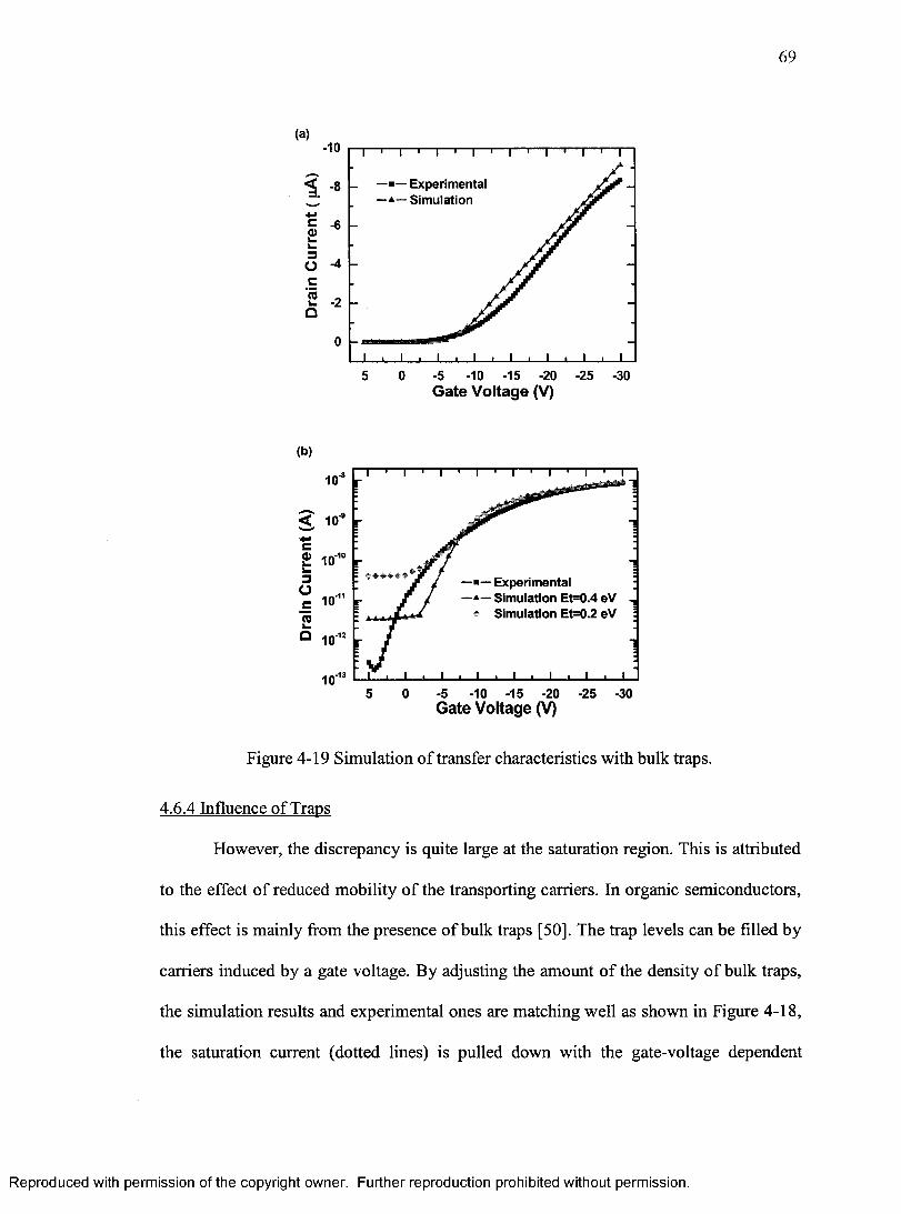
69
(a)-10
1— Experimental — Simulation
c1.1-3Oc■«5o
5 0 -5 -10 -15 -20 -25 -30Gate Voltage (V)
(b)
<c£ ,-10
3o — Experimental
— Simulation Et=0.4 eV ♦ Simulation Et=0.2 eV(QL .
Q ,-12
,-13
0 -5 -10 -15 -20 -25 -30Gate Voltage (V)
Figure 4-19 Simulation o f transfer characteristics with bulk traps.
4.6.4 Influence o f Traps
However, the discrepancy is quite large at the saturation region. This is attributed
to the effect o f reduced mobility o f the transporting carriers. In organic semiconductors,
this effect is mainly from the presence o f bulk traps [50]. The trap levels can be filled by
carriers induced by a gate voltage. By adjusting the amount o f the density o f bulk traps,
the simulation results and experimental ones are matching well as shown in Figure 4-18,
the saturation current (dotted lines) is pulled down with the gate-voltage dependent
Reproduced with permission of the copyright owner. Further reproduction prohibited without permission.
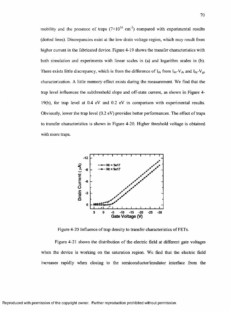
70
mobility and the presence of traps (7 xlo'^ cm'^) compared with experimental results
(dotted lines). Discrepancies exist at the low drain voltage region, which may result from
higher current in the fabricated device. Figure 4-19 shows the transfer characteristics with
both simulation and experiments with linear scales in (a) and logarithm scales in (b).
There exists little discrepancy, which is from the difference of Ids from Ids-Vds and Ids-Vgs
characterization. A little memory effect exists during the measurement. We find that the
trap level influences the subthreshold slope and off-state current, as shown in Figure 4-
19(b), for trap level at 0.4 eV and 0.2 eV in comparison with experimental results.
Obviously, lower the trap level (0.2 eV) provides better performances. The effect o f traps
to transfer characteristics is shown in Figure 4-20. Higher threshold voltage is obtained
with more traps.
-12
Nt = 5e17 ■ ^ N t = 9e171
+-•c0>1-l-3Oc
Q
05 -5 -10 -15 -20 -25 -30Gate Voltage (V)
Figure 4-20 Influence o f trap density to transfer characteristics o f FETs.
Figure 4-21 shows the distribution o f the electric field at different gate voltages
when the device is working on the saturation region. We find that the electric field
increases rapidly when closing to the semiconductor/insulator interface from the
Reproduced with permission of the copyright owner. Further reproduction prohibited without permission.
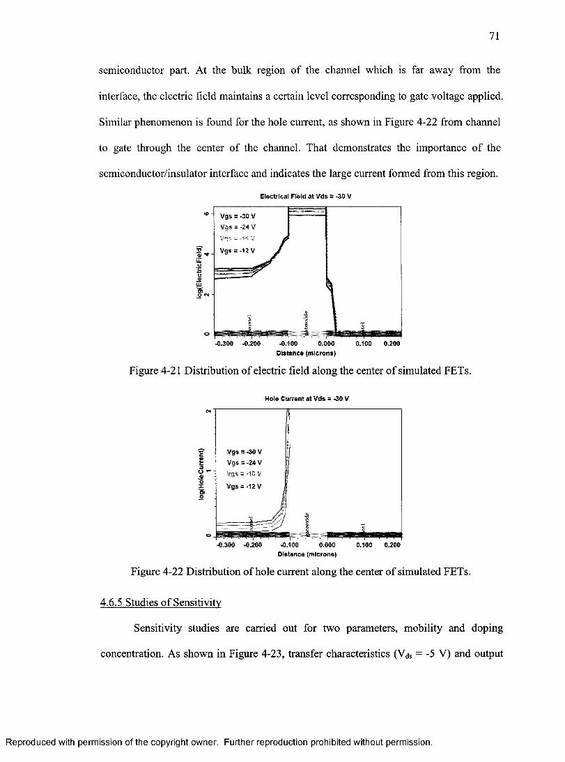
71
semiconductor part. At the bulk region o f the channel which is far away from the
interface, the electric field maintains a certain level corresponding to gate voltage applied.
Similar phenomenon is found for the hole current, as shown in Figure 4-22 from channel
to gate through the center o f the charmel. That demonstrates the importance o f the
semiconductor/insulator interface and indicates the large current formed from this region.
Electrical Field at Vds = -30 V
- Vgs = -30 VVgs = -24 V
Vgs = -12 V j filo•C
m 1o w -
1 t 1 $o . . .
-0.300 -0.200 -0.100 0.000 0.100 0.200Distance (microns)
Figure 4-21 Distribution o f electric field along the center o f simulated FETs.
Hole Current at Vds = -30 V
fc3U 'OoX
Vgs = -30 V 1Vgs = -24 V
: Vgs = -18 V 1Vgs = -12 V 1
J lm - '^ 7 IS
1 1
-0.300 -0.200 -0.100 0.000 0.100 0.200Distance (microns)
Figure 4-22 Distribution o f hole current along the center o f simulated FETs.
4.6.5 Studies o f Sensitivitv
Sensitivity studies are carried out for two parameters, mobility and doping
concentration. As shown in Figure 4-23, transfer characteristics (Vds = -5 V) and output
Reproduced with permission of the copyright owner. Further reproduction prohibited without permission.
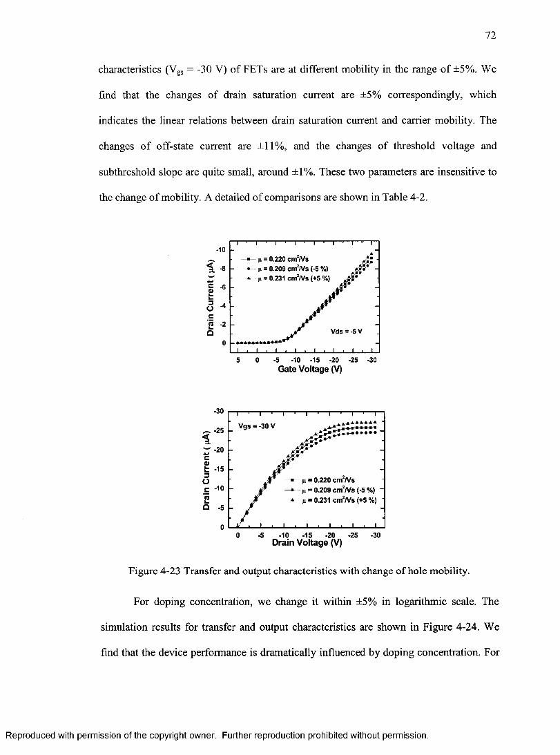
72
characteristics (Vgs = -30 V) of FETs are at different mobility in the range o f ±5%. We
find that the changes o f drain saturation current are ±5% correspondingly, which
indicates the linear relations between drain saturation current and carrier mobility. The
changes o f off-state current are ± 1 1 %, and the changes o f threshold voltage and
subthreshold slope are quite small, around ±1%. These two parameters are insensitive to
the change o f mobility. A detailed o f comparisons are shown in Table 4-2.
-10^ H = 0.220 cnfNs » H = 0.209 cmWs (-5 %) * H = 0.231 cmWs (+5 %)
1c0)L_fc-3oc
Vds = -5VQ
■10 -15 -20 -25 -305 0 ■5Gate Voltage (V)
T '---1—'—I—'---TVgs = -30 V
^ = 0.220 cm A/s H = 0.209 cmW s (-5 %) ^ = 0.231 cmW s (-f5 %)
J 1 I ■ I 1 I 1 I 1 L0 -5 -10 -15 -20 -25 -30
Drain Voltage (V)
Figure 4-23 Transfer and output characteristics with change of hole mobility.
For doping concentration, we change it within ±5% in logarithmic scale. The
simulation results for transfer and output characteristics are shown in Figure 4-24. We
find that the device performance is dramatically influenced by doping concentration. For
Reproduced with permission of the copyright owner. Further reproduction prohibited without permission.
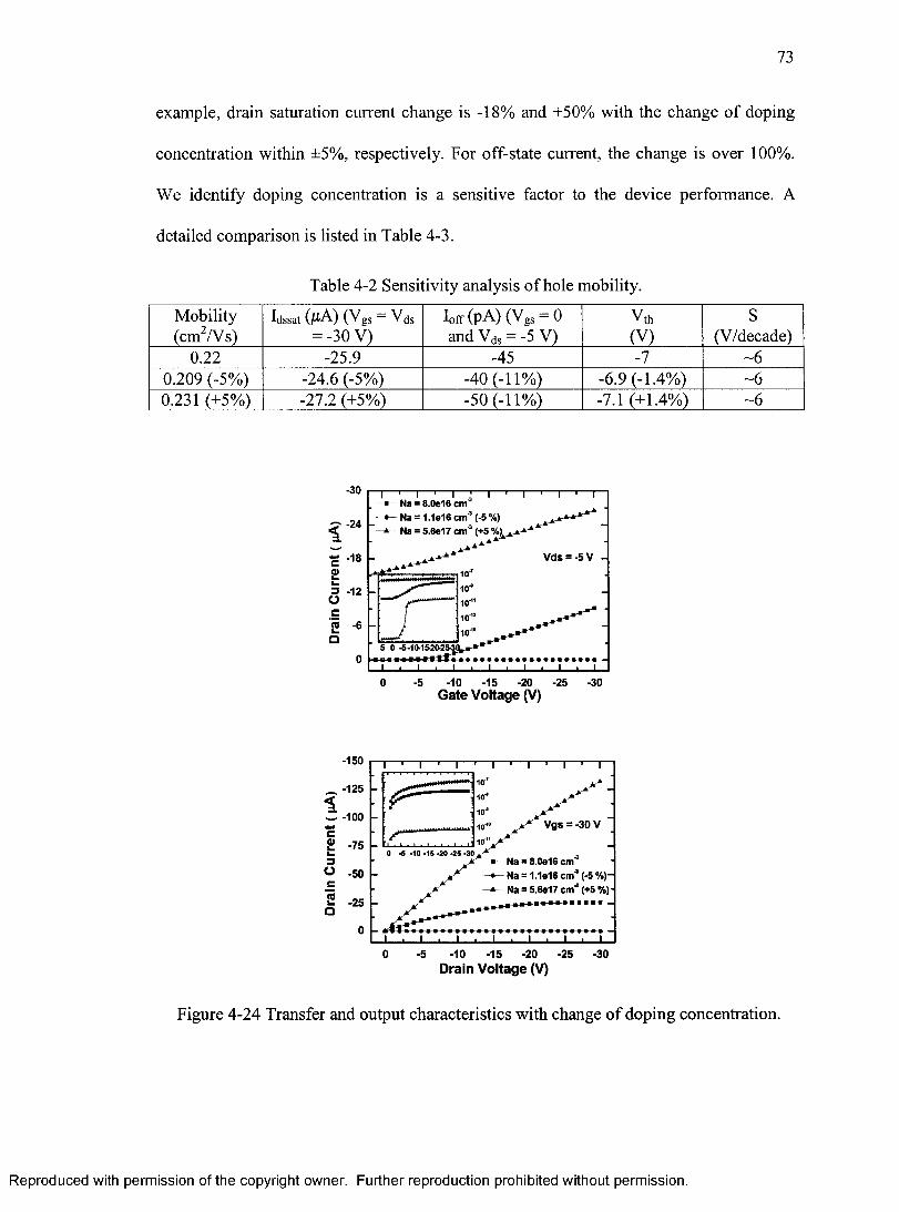
73
example, drain saturation current change is -18% and +50% with the change o f doping
concentration within ±5%, respectively. For off-state current, the change is over 100%.
We identify doping concentration is a sensitive factor to the device performance. A
detailed comparison is listed in Table 4-3.
Table 4-2 Sensitivity analysis o f hole mobility.
Mobility Idssat (M'A) (Vgs V(3s loff (pA) (Vgs = 0 Vth S(cm^/Vs) = -30 V) and Yds = -5 V) (V) (V/decade)
0 . 2 2 -25.9 -45 -7 ~ 6
0.209 (-5%) -24.6 (-5%) -40 (-11%) -6.9 (-1.4%) ~ 6
0.231 (+5%) -27.2 (+5%) -50 (-11%) -7.1 (+1.4%) ~ 6
1 —'—I—'—r n —I—'—I—— Na = S.0e16 cm
• Na = 1.1e16 cm"* (.5 %)* Na = 5.6e17 cm"’ (+5 %).
■ A-A*
C
£W3ac
Q
"I—'—rk-*
Vds = -5V
5 0 .5-10.1&20.2Sa
0 -5 -10 -15 -20 -25 -30Gate Voltage (V)
-150
^ -125
1— -100
£ -75
1—■—I—'—I—'—r1 0 '
10-1010 ’“
10” V
A'* Vgs = -30 V
O .500 .5 -10 -15 -20 -25 -30 i '* '
-.X * Na = 5.6e17 cm^ (+5 %)
Na = 8.0e16 cm Na = I . I 0 I 6 cm"* (-5 % )-
0 -J I I I L
-5 -10 -15 -20 -25 -30Drain Voltage (V)
Figure 4-24 Transfer and output characteristics with change o f doping concentration.
Reproduced with permission of the copyright owner. Further reproduction prohibited without permission.
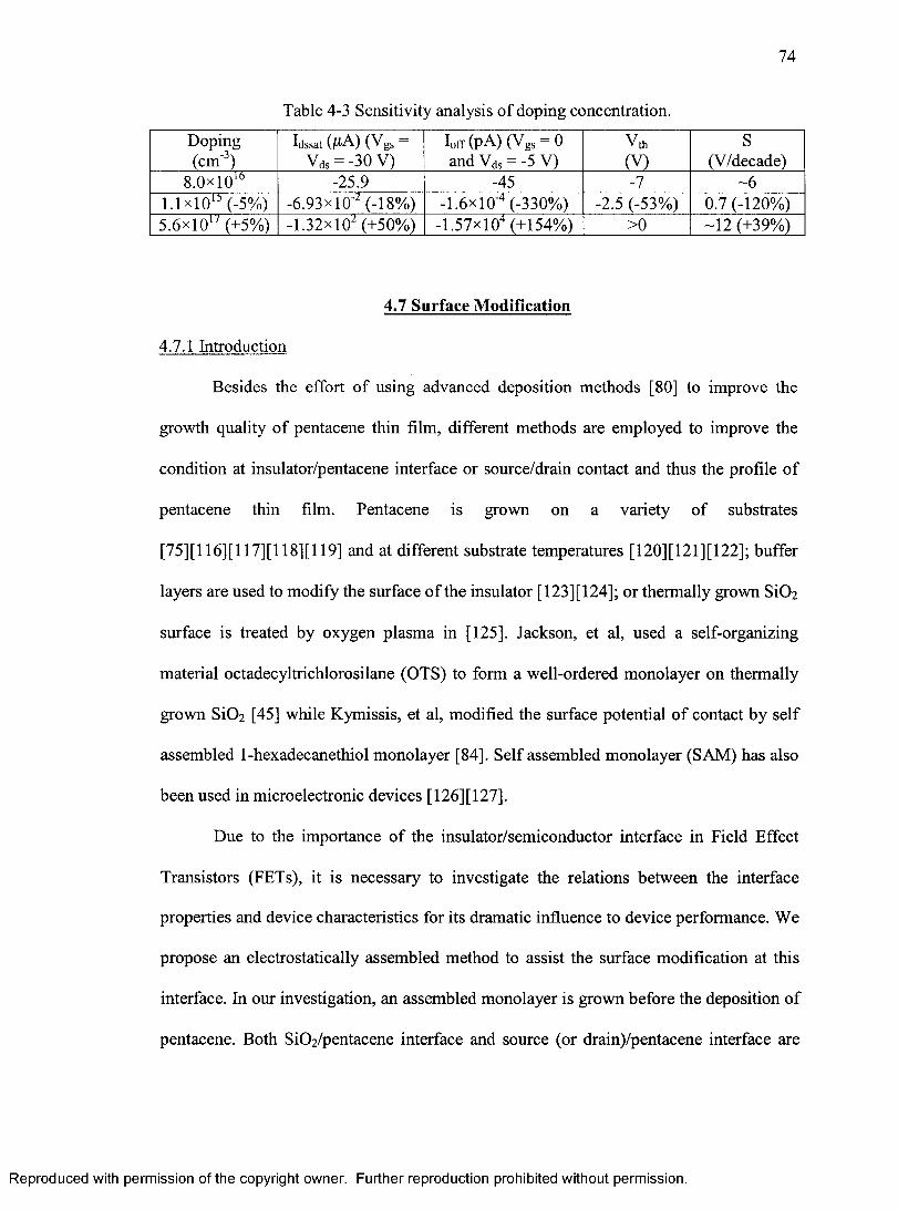
74
Table 4-3 Sensitivity analysis o f doping concentration.
Doping(cm‘ )
Idssat (/^A) (Vgs Yds = -30 V)
loff (pA) (Vgs = 0
and Yds = -5 V)Vth(V)
S(V/decade)
8 .0 x 1 0 *’ -25.9 -45 -7 ~ 6
1.1x10*" (-5%) -6.93x10'^ (-18%) -1.6x10'^ (-330%) -2.5 (-53%) 0.7 (-120%)5.6x10" (+5%) -1.32x10" (+50%) -1.57x10^ (+154%) > 0 -12 (+39%)
4.7 Surface Modiflcation
4.7.1 Introduction
Besides the effort o f using advanced deposition methods [80] to improve the
growth quality o f pentacene thin film, different methods are employed to improve the
condition at insulator/pentacene interface or source/drain contact and thus the profile of
pentacene thin film. Pentacene is grown on a variety o f substrates
[75][116][117][118][119] and at different substrate temperatures [120][121][122]; buffer
layers are used to modify the surface o f the insulator [123][124]; or thermally grown Si0 2
surface is treated by oxygen plasma in [125]. Jackson, et al, used a self-organizing
material octadecyltrichlorosilane (OTS) to form a well-ordered monolayer on thermally
grown Si0 2 [45] while Kymissis, et al, modified the surface potential o f contact by self
assembled 1-hexadecanethiol monolayer [84]. Self assembled monolayer (SAM) has also
been used in microelectronic devices [126] [127].
Due to the importance o f the insulator/semiconductor interface in Field Effect
Transistors (FETs), it is necessary to investigate the relations between the interface
properties and device characteristics for its dramatic influence to device performance. We
propose an electrostatically assembled method to assist the surface modification at this
interface. In our investigation, an assembled monolayer is grown before the deposition of
pentacene. Both Si0 2 /pentacene interface and source (or drain)/pentacene interface are
Reproduced with permission of the copyright owner. Further reproduction prohibited without permission.
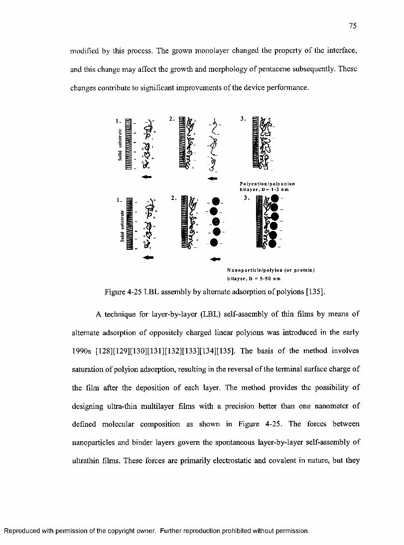
75
modified by this process. The grown monolayer changed the property o f the interface,
and this change may affect the growth and morphology o f pentacene subsequently. These
changes contribute to significant improvements of the device performance.
1 .
3.
P o l y c a t i o n / p o l y an ion b i l a y e r , D = 1- 2 nm
N a n o p a r t i c l e / p o l y i o n ( o r p r o t e i n )
b i l a y e r , D = 5 - 5 0 n m
Figure 4-25 LBL assembly by altemate adsorption o f polyions [135].
A technique for layer-by-layer (LBL) self-assembly o f thin films by means o f
altemate adsorption o f oppositely charged linear polyions was introduced in the early
1990s [128][129][130][131][132][133][134][135]. The basis o f the method involves
saturation o f polyion adsorption, resulting in the reversal o f the terminal surface charge o f
the film after the deposition o f each layer. The method provides the possibility o f
designing ultra-thin multilayer films with a precision better than one nanometer o f
defined molecular composition as shown in Figure 4-25. The forces between
nanoparticles and binder layers govem the spontaneous layer-by-layer self-assembly o f
ultrathin films. These forces are primarily electrostatic and covalent in nature, but they
Reproduced with permission of the copyright owner. Further reproduction prohibited without permission.
76
can also involve hydrogen bonding, hydrophobic and other types o f interactions. The
properties o f the self-assembled multilayers depend on the choice o f building blocks used
and their rational organization and integration along the axis perpendicular to the
substrate. Poly(dimethyldiallylammonium chloride) (PDDA) and poly(styrenesulfonate)
(PSS) are positive and negative polyions, respectively, which are commonly used
nanoparticles in self assembly technique as a precursor. By immersing the wafer in their
solution alternatively, a thin self assembled film can be obtained. Normally, PDDA is
grown firstly due to its good adhesion with substrates.
4.7.2 Experimental
A bottom-contact structure o f the fabricated devices is schematically shown in
Figure 4-9. Fabrication steps are similar except the presence o f the assembled monolayer.
First o f all, heavily-doped n-type silicon wafers were prepared and cleaned as the gate
electrode as well as the substrate. Second, 100 nm-thick layer o f Si0 2 is grown on the
silicon by thermal oxidation, and serving as the gate dielectric material. Subsequently, a
layer o f Au/Ti (80 nm/30 nm) is deposited by sputtering, followed by photolithography
and wet etching to pattern the Au/Ti source and drain (S/D) contacts.
Samples are then separated into two groups. Group One labeled as “without
assembled monolayer” is ready for pentacene evaporation. Samples in Group Two are
then treated with sulfuric acid and hydrogen peroxide solution (3:7) at 70°C for 3 minutes.
After that samples in Group Two are immersed in aqueous poly(dimethyldiallyl
ammonium chloride) (PDDA, MW 200,000, Sigma) solution at a concentration o f 15
mg/mL and pH 8 for 20 minutes. PDDA is the positively charged polyion, while Si0 2
surface is hydrophilic and shows negative charged after the treatment by the sulfliric acid
Reproduced with permission of the copyright owner. Further reproduction prohibited without permission.
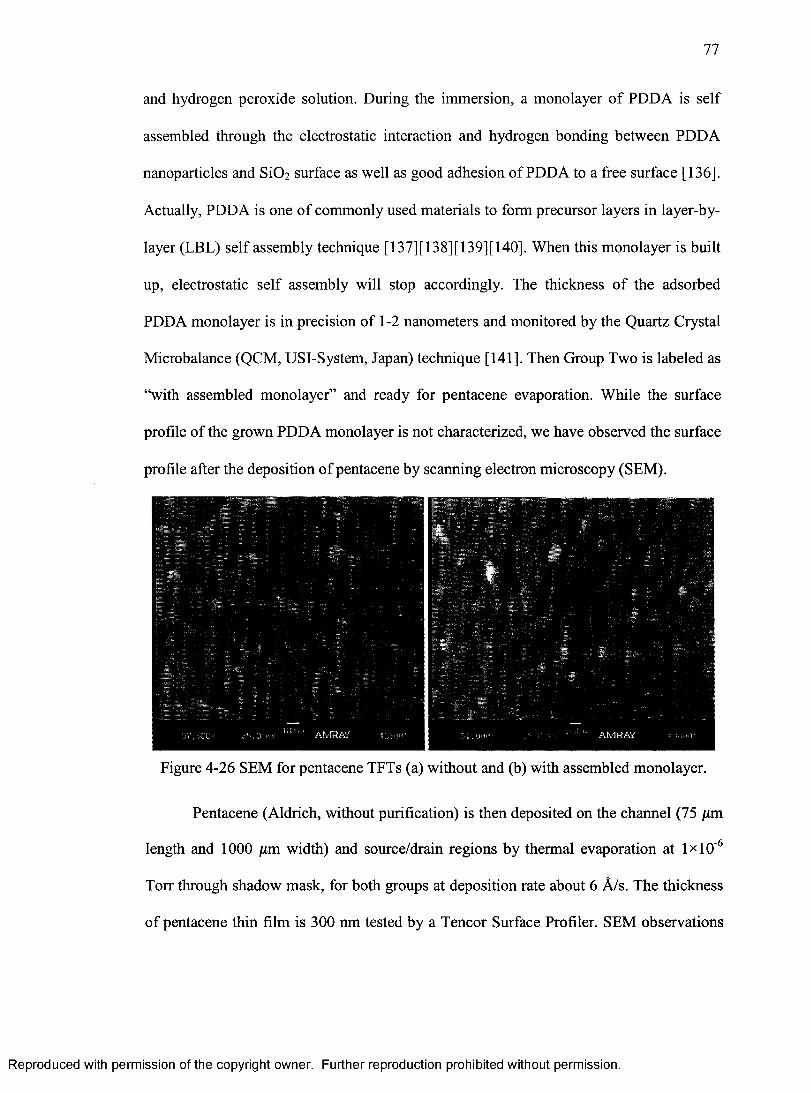
77
and hydrogen peroxide solution. During the immersion, a monolayer o f PDDA is self
assembled through the electrostatic interaction and hydrogen bonding between PDDA
nanoparticles and S1 0 2 surface as well as good adhesion of PDDA to a free surface [136].
Actually, PDDA is one o f commonly used materials to form precursor layers in layer-by-
layer (LBL) self assembly technique [137][138][139][140]. When this monolayer is built
up, electrostatic self assembly will stop accordingly. The thickness o f the adsorbed
PDDA monolayer is in precision o f 1-2 nanometers and monitored by the Quartz Crystal
Microbalance (QCM, USI-System, Japan) technique [141]. Then Group Two is labeled as
“with assembled monolayer” and ready for pentacene evaporation. While the surface
profile o f the grown PDDA monolayer is not characterized, we have observed the surface
profile after the deposition o f pentacene by scanning electron microscopy (SEM).
Figure 4-26 SEM for pentacene TFTs (a) without and (b) with assembled monolayer.
Pentacene (Aldrich, without purification) is then deposited on the charmel (75 jmx
length and 1 0 0 0 jam width) and source/drain regions by thermal evaporation at 1 x 1 0 ’
Torr through shadow mask, for both groups at deposition rate about 6 A/s. The thickness
o f pentacene thin film is 300 nm tested by a Tencor Surface Profiler. SEM observations
Reproduced with permission of the copyright owner. Further reproduction prohibited without permission.
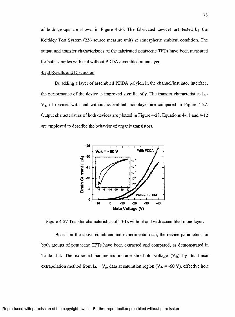
78
of both groups are shown in Figure 4-26. The fabricated devices are tested by the
Keithley Test System (236 source measure unit) at atmospheric ambient condition. The
output and transfer characteristics o f the fabricated pentacene TFTs have been measured
for both samples with and without PDDA assembled monolayer.
4.7.3 Results and Discussion
Be adding a layer o f assembled PDDA polyion in the channel/insulator interface,
the performance o f the device is improved significantly. The transfer characteristics Ids-
Vgs of devices with and without assembled monolayer are compared in Figure 4-27.
Output characteristics o f both devices are plotted in Figure 4-28. Equations 4-11 and 4-12
are employed to describe the behavior o f organic transistors.
-25With PDDA• Vds = - 60 V
^ -20
-15
-10
Without PDDA
10 0 -30 ■40-10 -20
Gate Voltage (V)
Figure 4-27 Transfer characteristics o f TFTs without and with assembled monolayer.
Based on the above equations and experimental data, the device parameters for
both groups o f pentacene TFTs have been extracted and compared, as demonstrated in
Table 4-4. The extracted parameters include threshold voltage (Vth) by the linear
extrapolation method from Ids - Vgs data at saturation region (Yds = -60 V), effective hole
Reproduced with permission of the copyright owner. Further reproduction prohibited without permission.
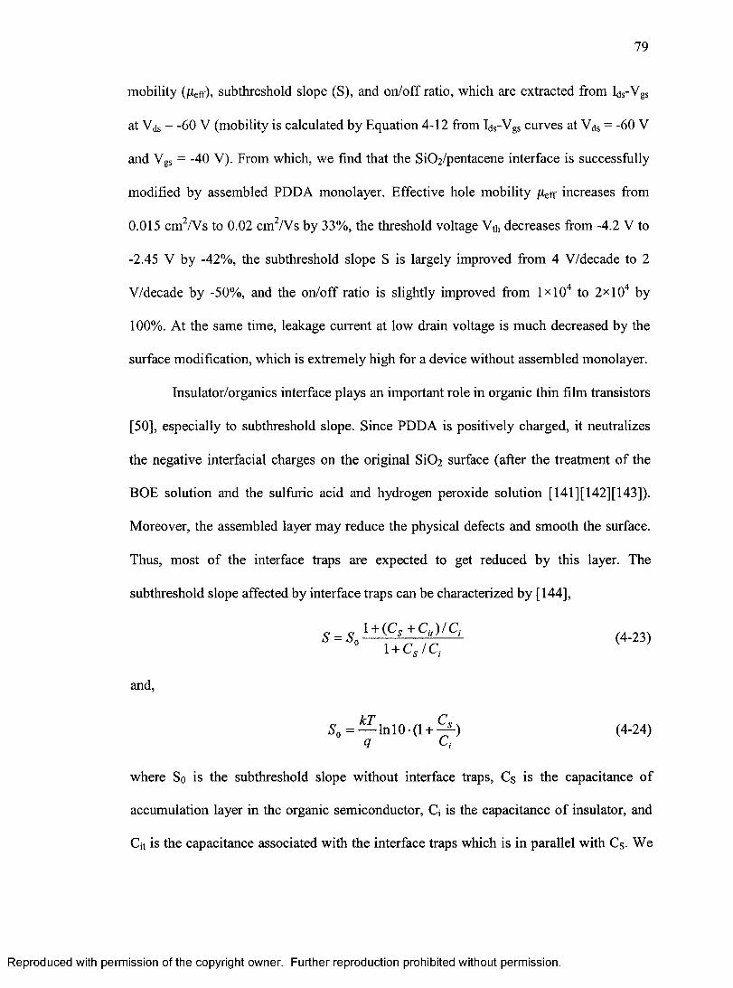
79
mobility (jiteff), subthreshold slope (S), and on/off ratio, which are extracted from Ids-Vgs
at Yds = -60 V (mobility is calculated by Equation 4-12 from Ids-Vgs curves at Yds = -60 Y
and Ygs = -40 Y). From which, we find that the Si0 2 /pentacene interface is successfully
modified by assembled PDDA monolayer. Effective hole mobility jUeff increases from
0.015 cm^/Ys to 0.02 cm^/Ys by 33%, the threshold voltage Yth decreases from -4.2 Y to
-2.45 Y by -42%, the subthreshold slope S is largely improved from 4 Y/decade to 2
Y/decade by -50%, and the on/off ratio is slightly improved from IxlO"* to 2x10" by
100%. At the same time, leakage current at low drain voltage is much decreased by the
surface modification, which is extremely high for a device without assembled monolayer.
Insulator/organics interface plays an important role in organic thin film transistors
[50], especially to subthreshold slope. Since PDDA is positively charged, it neutralizes
the negative interfaeial charges on the original Si0 2 surface (after the treatment o f the
BOE solution and the sulfuric acid and hydrogen peroxide solution [141][142][143]).
Moreover, the assembled layer may reduce the physical defects and smooth the surface.
Thus, most o f the interface traps are expected to get reduced by this layer. The
subthreshold slope affeeted by interface traps can be characterized by [144],
5 = ■S£Ll9ltlL£L (4_23)l + Q /C ,.
and,
kT C5 o = — lnlO -(l + ^ ) (4-24)
q C,
where So is the subthreshold slope without interface traps, Cs is the capacitance o f
accumulation layer in the organic semiconductor, Ci is the capacitance o f insulator, and
Cit is the capacitance associated with the interface traps which is in parallel with Cs- We
Reproduced with permission of the copyright owner. Further reproduction prohibited without permission.
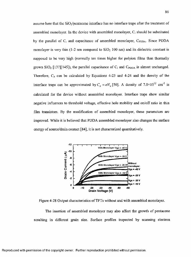
80
assume here that the Si0 2 /pentacene interface has no interface traps after the treatment of
assembled monolayer. In the device with assembled monolayer, Ci should be substituted
by the parallel o f C i and capacitance o f assembled monolayer, C p d d a - Since PDDA
monolayer is very thin ( 1 - 2 nm compared to SiOa 1 0 0 nm) and its dielectric constant is
supposed to be very high (normally ten times higher for polyion films than thermally
grown Si0 2 [ 1 3 7 ] [ 1 4 5 ] ) , the parallel capacitance of C i and C p d d a is almost unchanged.
Therefore, C i t can be calculated by Equations 4 - 2 3 and 4 - 2 4 and the density o f the
interface traps can be approximated byC,-, [ 5 0 ] . A density o f 7 . 0 x 1 0 ' ^ cm'^ is
calculated for the device without assembled monolayer. Interface traps show similar
negative influences to threshold voltage, effective hole mobility and on/off ratio in thin
film transistors. By the modification o f assembled monolayer, these parameters are
improved. While it is believed that PDDA assembled monolayer also changes the surface
energy o f source/drain contact [84], it is not characterized quantitatively.
-12 1 — '— I— '— rWith Monolayer: Vgs = -40 V'
Monolayer
Monolayer:Vgs
With Monolayer:Vgs = -10 V
Without monolayer: Vgs = -40 V
Vgs = -30 V
Vgs = -20 V Vgs = -10 V
-10 -20 -30 -40 -50 -60Drain Voltage (V)
Figure 4-28 Output characteristics o f TFTs without and with assembled monolayer.
The insertion o f assembled monolayer may also affect the growth o f pentacene
resulting in different grain size. Surface profiles inspected by scanning electron
Reproduced with permission of the copyright owner. Further reproduction prohibited without permission.
81
microscopy (SEM) are shown in Figure 4-26. Surface profile without assembled
monolayer shows irregular grain size with clear grain boundaries (Figure 4-26(a)), caused
by an untreated surface. After the treatment o f assembled monolayer, the surface
condition are much improved and yield better surface profile o f pentacene, as
demonstrated in Figure 4-26(b), with smoother grain, more uniform grain size, and blurry
grain boundaries though smaller.
The investigations and results presented here show that PDDA nano-scaled
polyion can be used to modify the surface between insulator and active material in thin
film transistors. By the immersion in the aqueous solution, PDDA nanoparticles form an
ordered monolayer on Si0 2 through electrostatic self assembly. By the influence to the
Si0 2 /pentacene interface, the device performance is improved including higher effective
mobility, lower threshold voltage, and lower subthreshold slope, etc.
Table 4-4 Comparison o f pentacene TFTs without and with assembled monolayer.
Vth(V) jaeff(cm^Ws) S (V/decade) on/off ratioWithout assembled
monolayer -4.20 0.015 4 1 0 ^
With assembled -2.45 0 . 0 2 0 2 2 x 1 0 ^monolayer (-42%) (33%) (-50%) ( 1 0 0 %)
Reproduced with permission of the copyright owner. Further reproduction prohibited without permission.
CHAPTER FIVE
CONCLUSIONS AND FUTURE WORK
5.1 Conclusions
In this project, organic microelectronic devices including capacitors, Schottky
diodes, and field-effect transistors have been fabricated, characterized, and modeled.
Main fabrication techniques used here include spin-coating, thermal evaporation, photo
lithography, electrostatic self assembly, and reactive ion etching. Numerical simulation
tools, Taurus-Device and Medici (Synopsys®) are employed to model and simulate the
fabricated devices.
From the capacitance-voltage (C-V) characteristics o f the fabricated organic
capacitors, consisting o f insulating polymer poly(4-vinylphenol) (PVP), the dielectric
constant o f PVP is determined in both metal-insulator-metal (MIM) and metal-insulator-
semiconductor (MIS) structures, and the dielectric constant is found to be in the range of
5.6 - 5.94. The MIS structure is preferred over the MIM structure due to relatively
simpler fabrication process steps and higher stability o f the device characteristics.
Pentacene is a commonly used organic semiconductor, whose hole density is determined
to be about 8x10^^ cm'^ from the MIS structure.
Based on the fabrication and characterization o f Poly[2-methoxy-5-(2’-ethyl-
hexyloxy)-!,4-phenylene vinylene] MEH-PPY Schottky diodes, electrical characteristics
82
Reproduced with permission of the copyright owner. Further reproduction prohibited without permission.
83
including temperature-dependent mobility have been experimentally and theoretically
investigated based on the current density-voltage (J-V) and capacitance-voltage (C-V)
characteristics. To the best of our knowledge, this is the first investigation on the
temperature dependence of mobility for MEH-PPY above the room temperature. As a
part of this work, the space-charge limited conduction model and the field-dependent
mobility model have been examined. They can describe the behavior o f the fabricated
Schottky diodes. The highest measured hole mobility o f MEH-PPY is 0.013 cm^A^s at
353 K from the fabricated Schottky diodes. The effective carrier density o f MEH-PPY is
calculated to be 2.24x10^^ cm'^, which is useful for the simulation o f the MEH-PPY
based Schottky diodes. Several important factors, including barrier height and bulk traps
are derived from simulations, which should be considered in the design o f experiments
and structures for Schottky diodes.
The organic field-effect transistors are investigated for n-type oligomer
Naphthalene-tetracarboxylic-dianhydride (NTCDA). The NTCDA based transistors work
on the depletion mode with a novel design consisting o f organic dielectric, channel, and
source/drain regions. The device characteristics have displayed the electron mobility o f
0.016 cm^A^s, threshold voltage o f -32 Y, and on/off ratio of 2.25 x 10 .
For field-effect transistors consisting of p-type organic semiconductor pentacene,
the temperature dependence o f mobility is studied experimentally, which also seems to be
the first investigation for mobility above the room temperature. The deposition rate o f
pentacene affects the performance o f the field-effect transistors. At room temperature, the
device characteristics have displayed the hole mobility o f 0.26 cm N s, threshold voltage
o f -3.5 Y, subthreshold slope o f 2.5 Y/decade, and on/off ratio o f 10^ for the lower
Reproduced with permission of the copyright owner. Further reproduction prohibited without permission.
84
2deposition rate o f pentacene, and the hole mobility is 0.003 cm N s, threshold voltage of
2.5 V, subthreshold slope of 6 V/decade, and on/off ratio of 10 for the higher deposition
rate of pentacene. The transistors with the lower deposition rate o f pentacene offer better
device performance. This demonstrates the importance of process control. Numerical
simulations identify the effect o f field dependence o f mohility and the influence o f bulk
traps, which are crucial to the operation o f organic field-effect transistors.
At last, the insulator/semiconductor interface is modified by electrostatically
assembled monolayer (Poly(dimethyldiallylammonium chloride) (PDDA)). With the
treatment o f this assembled monolayer, the performance of pentacene FETs is improved
significantly including higher effective hole mobility by 33%, lower threshold voltage by
-42%, and lower subthreshold slope by -50%. This appears to be the first application of
electrostatically assembled monolayer in field-effect transistors to our knowledge. This
technique can be extended to other devices such as capacitors and diodes for the
performance improvement.
5.2 Future Work
The field o f organic electronics is still under development. Though conducting
polymer/oligomer has disadvantages, such as high resistivity and low carrier mobility,
these parameters have been much improved during the last three decades. The
performance o f organic electronic devices and circuits will be further improved
continually with the studies in material properties, device structures, and fabrication
techniques.
Several works can be considered for the extension of this project in the future. For
organic capacitors, electrostatically assembled monolayer can be introduced to
Reproduced with permission of the copyright owner. Further reproduction prohibited without permission.
85
organic/metal or insulator/organic interface to improve the device performance.
Furthermore, new and better materials can take the place o f PVP as an insulator and
pentacene as an active layer. The frequency dependence o f capacitance o f organic
capacitors can be investigated. Further simulations can be carried out based on better
understanding o f the conduction mechanism o f organics.
For Schottky diodes, an electrostatically assembled monolayer can be introduced
to organic/metal or insulator/organic interface o f MEH-PPY Schottky diodes for
improvement. The space-charge limited conduction model and field-dependent mobility
model can be developed and applied in numerical simulation, which will benefit the
studies o f conduction mechanism in organic materials. New models can be generated
with the aid o f simulation and modeling. Furthermore, light-emitting diodes and solar
cells can be developed based on the fabricated Schottky diodes. More than one layer of
organics can be involved in the light-emitting diodes and solar cells to improve the
performance o f devices.
Since the reactive ion etching technique is employed in the experiments, the
degradation o f organics may be introduced by this process. By etching organics other
than oxygen in reactive ion etching, the degradation can be estimated or determined.
For field-effect transistors, fabrication techniques like the ink-jet printing and
novel device structures such the dual-gate and three dimensional structures can be
proposed to improve the device performance. The investigation on temperature
dependence o f mobility can be extended to a wider range. Numerical simulation can be
employed for device performance optimization. Experiments can be performed to verify
the optimal design.
Reproduced with permission of the copyright owner. Further reproduction prohibited without permission.
86
The experiments can be proposed to characterize the properties o f the
electrostatically assembled monolayer. Electrostatically assembled monolayer can be
further studied to yield better improvements. Other nanoparticles, like
poly(styrenesulfonate) (PSS), and more layers o f assembled nanoparticles can be tested
for their effects on the device performance.
Furthermore, organic light-emitting diodes and organic field-effect transistors can
be combined together to realize organic active-matrix displays. All o f these investigations
may contribute and benefit the development o f organic electronics.
Reproduced with permission of the copyright owner. Further reproduction prohibited without permission.
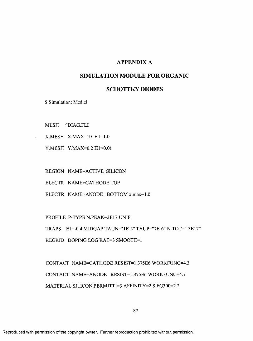
APPENDIX A
SIMULATION MODULE FOR ORGANIC
SCHOTTKY DIODES
$ Simulation: Medici
MESH ^DIAG.FLI
X.MESH X.MAX=10 Hl=1.0
Y.MESH Y.MAX=0.2 Hl=0.01
REGION NAME=ACTIVE SILICON
ELECTR NAME=CATHODE TOP
ELECTR NAME=ANODE BOTTOMx.max=I.O
PROFILE P-TYPEN.PEAK=3E17UNIF
TRAPS El=-0.4 MIDGAP TAUN=’TE-5" TAUP='TE-6 " N.TOT="-3E17"
REGRID DOPING LOG RAT=3 SM 00TH=1
CONTACT NAME=CATHODE RESIST=1.375E6 WORKFUNC=4.3
CONTACT NAME=ANODE RESIST=1.375E6 WORKFUNC=4.7
MATERIAL SILICON PERMITTI=3 AFFINITY=2.8 EG300=2.2
87
Reproduced with permission of the copyright owner. Further reproduction prohibited without permission.
88
MATERIAL SILICON NC300=1E21 NV300=IE21
MOBILITY SILICON MUP0=0.00006
MODELS SRH AUGER
SYMB NEWTON CARRIERS=1 HOLE
LOG OUT.FILE-iv_50.ivl
SOLVE V(CATHODE)=0.0
SOLVE V(ANODE)=-5.0 ELEC-ANODE VSTEP-0.1 NSTEP-IGG
SAVE 0UT.FILE-SI-5G
$ END OF INPUT.
Reproduced with permission of the copyright owner. Further reproduction prohibited without permission.
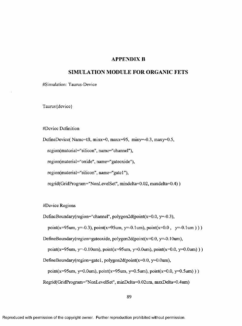
APPENDIX B
SIMULATION MODULE FOR ORGANIC FETS
#Simulation: Taurus-Device
Taurus {device}
#DeYice Definition
DefineDevice( Name=tft, minx=0, maxx=95, miny=-0.3, maxy=0.5,
region(material=" silicon", name="channel"),
region(material="oxide", name="gateoxide"),
region(material="silicon", name="gatel"),
regrid(GridProgram="NonLevelSet", mindelta=0.02, maxdelta=0.4))
#Device Regions
DefineBoundary(region="channel", polygon2d(point(x=0.0, y=-0.3),
point(x=95um, y=-0.3), point(x=95um, y=-0.1um), point(x=0.0 , y=-0.1um ) ) )
DefineBoundary(region=gateoxide, polygon2d(point(x==0.0, y=-0.1 Oum),
point(x=95um, y=-0.10um), point(x=95um, y=O.Oum), point(x=0.0, y=O.Oum) ) )
DefineBoundary(region=gatel, polygon2d(point(x=0.0, y=O.Oum),
point(x=95um, y=O.Oum), point(x=95um, y=0.5um), point(x=0.0, y=0.5um) ) )
Regrid(GridProgram="NonLevelSet", minDelta=0.02um, maxDelta=0.4um)
89
Reproduced with permission of the copyright owner. Further reproduction prohibited without permission.
90
Regrid(GridProgram="NonLevelSet", minDelta=0.01 um, maxDelta=0.2um)
Regrid(GridProgram="NonLevelSet", minDelta=0.02um, maxDelta=0.2um,
minY=0.0,maxY=0.1um, minX=7.5um, maxX=12.5um)
Regrid(GridProgram="NonLevelSet", minDelta=0.02um, maxDelta=0.2um,
minY=0.0um,maxY=0.1um, minX=82.5um, maxX=87.5um)
#Flat Contacts
DefineContact(name=source, X(min=0.0, max=10um), Y(min=-0.21, max=-0.1um))
DefineContact(name=drain, X(min=85um, max=95um), Y(min=-0.21um, max=-0.1um))
DefineContact(name=gate, X(mm=0.0, max=95um), Y(min=0.5um, m ax=0.5um))
Contact(name=drain, workfunction=5.0)
Contact(name=source, workfunction=5.0)
Contact(name=gate, workfunction=4.1)
#Doping
Profile(name=Ptype, uniform(value=8 e l 6 ), region=channel)
Profile(name=Ntype, uniform(value=2e20), region^gatel)
setBias(value= 0.0) {Contact(name=drain, type=contactVoltage){tft} }
setBias(value= 0.0) {Contact(name=source, type=contactVoltage){tft} }
setBias(value= 0.0) {Contact(name=gate, type=contactVoltage){tft} }
setAttributes {Traps(material=silicon, region=channel,
Reproduced with permission of the copyright owner. Further reproduction prohibited without permission.
91
trap(ilevel=0, dgen=2, et=-0.4, n t= -le l6 , taup= le-5))}
Physics(silicon(HoleContinuity(Mobility (Constant=trae, mup0=0.045)))
Physics(Global(Global(ConductionDensityOfStates (AtRoomTemperature= 1 e21),
ValenceDensityOfStates (AtRoomTemperature=le21), Bandgap (Eg300=1.8)) ) )
Physics(Silicon(Global(Permittivity=^3, ElectronAffinit)F=3.2, WorkEunction==4.6)) )
# Specify zero-carrier solution
Solve{couple(iterations=50, LinearSolvei^direct){Poissons} }
# Specify one-carrier solution with electrons
Symbolic (carriers=2)
# Solve Output Characteristics
Solve {Ramp(RampSpecification( endValue=-6 , nsteps=6 )
{BiasObject(name=gate, type=ContactVoltage){tft} } )
{couple( iterations=20, LinearSolver=direct)
{Poissons, ElectronContinuity, HoleContinuity} } }
solve {ramp(rampSpecification(endValue=-31, nsteps=31)
{BiasObject(type=contactVoltage, nam e=drain)} )}
# End o f program.
Reproduced with permission of the copyright owner. Further reproduction prohibited without permission.
REFERENCES
[1] J. M. Shaw, P. F. Seidler, “Organic electronics: Introduction,” IBM J. Res. & Dev. 45 (2001) 3-9.
[2] M. Angelopoulos, “Conducting polymers in microelectronics,” IBM J. Res. & Dev. 45 (2001) 57-75.
[3] C. D. Dimitrakopoulos, D. J. Mascaro, “Organic thin-film transistors: A review of recent advances,” IBM J. Res. & Dev. 45 (2001) 11-27.
[4] G. Horowitz, D. Fichou, X. Peng, Z. Xu, F. Gamier, “A field-effect transistor based on conjugated alpha-sexithienyl,” Solid State Commun. 72 (1989) 381.
[5] F. Gamier, R. Hajlaoui, A. Yasser, P. Srivastava, “All polymer field-effect transistors realized by printing techniques,” Science 265 (1994) 1684.
[6 ] J. H. Burroughes, C. A. Jones, R. H. Friend, “New semiconductor device physics in polymer diodes and transistors,” Nature 335 (1988) 137.
[7] Z. Bao, A. Dodabalapur, A. Lovinger, “Soluble and processable regioregular poly(3- hexylthiophene) for thin film transistor applications with high mobility,” Appl. Phys. Lett. 69 (1996) 4108.
[8 ] R. Brown, A. Pomp, C. M. Hart, D. M. de Leeuw, “Logic gates made from polymer transistors and their use in ring oscillators,” Science 270 (1995) 972.
[9] Y. Lin, D. J. Gundlach, S. Nelson, T. N. Jackson, “Stacked pentacene layer organic thin-film transistor with improved characteristics,” IEEE Electron Device Lett. 18 (1997) 606.
[10] A. Dodabalapur, L. Torsi, H. E. Katz, “Organic transistors: Two-dimensional transport and improved electrical characteristics,” Science 268 (1995) 270.
[11] D. Dimitrakopoulos, S. Pumshothaman, J. Kymissis, A. Callegari, J. M. Shaw, “Low voltage transistors on plastic comprising high-dielectric-constant gate insulators,” Science 283 (1999) 822.
[12] J. W. Gardner, P. N. Bartlett, “Applications o f conducting polymer technology in microsystems,” Sources and Actuators A 51 (1995) 57-66.
92
Reproduced with permission of the copyright owner. Further reproduction prohibited without permission.
93
13] D. E. Bomside, C. W. Macosko, L. E. Scriven, “Modeling o f spin coating,” J. Imaging Technology 13 (1987) 122-130.
14] H. Klauk, D. J. Gundlach, T. N. Jackson, “Fast organic thin film transistor circuits,”IEEE Electron Device Lett. 20 (1999) 289-291.
15] E[. Klauk, D. J. Gundlach, et al., “Pentacene organic thin-film transistors and ICs,”Solid State Technology 43 (2000) 63-77.
16] T. R. Hebner, C. C. Wu, D. Marcy, M. H. Lu, J. C. Sturm, “Ink-jet printing of doped polymers for organic light emitting devices,” Appl. Phys. Lett. 72 (1998) 519-521.
17] S. C. Chang, J. Liu, J. Bharathan, Y. Yang, J. Onohara, J. Kido, “Multicolor organic light-emitting diodes processed by hybrid inkjet printing,” Adv. Mater. 11 (1999) 734.
18] Z. Bao, J. A. Rogers, H. E. Katz, “Printable organic and polymeric semiconducting materials and devices,” J. Mater. Chem. 9 (1999) 1895-1904.
19] C. N. Sayre, D. M. Collard, “Deposition o f polyaniline on micro-contact printed selfassembled monolayers o f w-fimctionalized alkanethiols,” J. Mater. Chem. 7 (1997) 909-912.
20] J. A. Rogers, Z. Bao, A. Makhija, P. Braun, “Printing process suitable for reel-to-reel production o f high-performance organic transistors and circuits,” Adv. Mater. 11 (1999)741.
21] A. J. Heeger, “Nobel lecture: Semiconducting and metallic polymers: The fourthgeneration o f polymeric materials,” Rev. Mod. Phys. 73 (2001) 681.
22] L. I. Malysheva, A. I. Onipko, “Exact solution for the Huckel model of hetropolyenes,” Synthetic Metals 80 (1996) 11-23.
23] B. Norden, E. Krutmeijer, “The Nobel prize in chemistry, 2000: Conductive polymers,” Kungl. Vetenskapsakademien, The Royal Swedish Academy o f Sciences.
24] A. G. MacDiarmid, “Nobel lecture: “Synthetic metals”: A novel role for organic polymers,” Rev. Mod. Phys. 73 (2001) 701-712.
25] R. A. Marcus, “Theory o f oxidation-reduction reactions involving electron-transfer,” J. Chem. Phys. 24 (1956) 966-978.
26] R. W. Dutton, “TCAD - Yesterday, today and tomorrow,” lEICE Trans. Electron. E82-C (1999) 791-799.
27] H. K. Gummel, “A self-consistent iterative scheme for one-dimensional steady state transistor calculations,” IEEE Trans. Electron Devices 11 (1964) 455-465.
Reproduced with permission of the copyright owner. Further reproduction prohibited without permission.
94
[28] P. E. Cottrell, E. M. Buturla, “Steady-state analysis of field effect transistors via thefinite element method,” lEDM Tech. Digest, (1975) 51-54.
[29] S. Selberherr, A. Schutz, H. W. Potzl, “MINIMOS— A two-dimensional MOS transistor analyzer,” IEEE Trans. Electron Devices ED-27 (1980).
[30] M. R. Pinto, C. S. Rafferty, R. W. Dutton, “PISCES II: Poisson and continuityequation solver,” Stanford Electronics Laboratories (1984).
[31] T. Mori; A. Shibuya, S. Yamamichi, “High-capacitance thin-film capacitors on a polymer film,” Japanese Joumal o f Applied Physics, Part 1: Regular Papers and Short Notes and Review Papers 42 (2003) 7432-7435.
[32] Y. Liu, T. Cui, K. Varahramyan, “All-polymer capacitor fabricated with inkjet printing technique,” Solid-State Electronics 47 (2003) 1543-1548.
[33] Y. Xu, P. Berger, J. Cho, R. B. Timmons, “Capacitance-voltage characterization o f pulsed plasma polymerized allylamine dielectrics,” Materials Research Society Symposium - Proceedings 736 (2002) 195-200.
[34] Y. Liu, T. Cui, K. Varahramyan, “Fabrication and characteristics o f polymeric thin-film capacitor,” Solid-State Electronics 47 (2003) 811-814.
[35] M. White, R. C. T. Slade, “Polymer electrodes doped with heteropolymetallates and their use within solid-state supercapacitors,” Synthetic Metals 139 (2003) 123-131.
[36] B. Chen, T. Cui, Y. Liu, K. Varahramyan, “All-polymer RC filter circuits fabricated with inkjet printing technology,” Solid-State Electronics 47 (2003) 841-847.
[37] Polysciences, Inc. http://www.poIysciences.com/
[38] M. Halik, H. Klauk, U. Zschieschang, G. Schmid, W. Radlik, S. Ponomarenko, S. Kirchmeyer, W. Weber, “High-mobility organic thin-film transistors based on oc,a’- didecyloligothiophenes,” J. Appl. Phys. 93 (2003) 2977-2981.
[39] S. Scheinert, G. Paasch, M. Schrodner, H. -K. Roth, S. SensfuB, Th. Doll, “Subthreshold characteristics o f field effect transistors based on poly(3- dodecylthiophene) and an organic insulator,” J. Appl. Phys. 92 (2002) 330-337.
[40] D. B. Wolfe, J. Christopher, B. D. Gates, G. M. Whitesides, R. S. Conroy, M. Prentiss, “Fabrication o f planar optical waveguides by electrical microcontact printing,” Appl. Phys. Lett. 84 (2004) 1623-1625.
[41] K. K. Ng, Complete Guide to Semiconductor Devices, 2nd edition, John Wiley & Sons, 2002.
[42] E. S. Yang, Microelectronic Devices, McGraw-Hill, 1988.
Reproduced with permission of the copyright owner. Further reproduction prohibited without permission.
95
[43] N. Arora, MOSFET models for VLSI circuit simulation: theory and practice, Springer Verlag, 1993.
[44] H. C. Casey, Devices for Integrated Circuits: Silicon and III-V CompoundSemiconductors, John Wiley & Sons, 1999.
[45] T. N. Jackson, Y. Y. Lin, D. J. Gundlach, H. Klauk, “Organic thin-film transistors for organic light-emitting flat-panel display backplanes,” IEEE Joumal o f Selected Topics in Quantum Electronics 4 (1998) 100-104.
[46] Y. S. Lee, J. H. Park, J. S. Choi, “Electrical characteristics o f pentacene-basedSchottky diodes,” Optical Materials 21 (2002) 433-437.
[47] G. Paasch, S. Scheinert, “Simulation and modeling of C-V curves o f OLEDs with traps states for the holes,” Synthetic Metals 122 (2001) 145-147.
[48] S. Scheinert, G. Paasch, S. Pohlmann, H. -H . Horhold, R. Stockmann, “Field effect in organic devices with solution-doped arylamino-poly-(phenylene-vinylene),” Solid- State Electronics 44 (2000) 845-853.
[49] E. J. Meijer, C. Tanase, P. W. M. Blom, E. van Veenendaal, B. -H . Huisman, D. M. de Leeuw, “Switch-on voltage in disordered organic field-effect transistors,” Appl. Phys. Lett. 80 (2002) 3838.
[50] J. H. Schon, B. Batlogg, “Trapping in organic field-effect transistors,” J. Appl. Phys.89 (2001) 336-342.
[51] J. Yoon, J. Kim, T. Lee, O. Park, “Evidence of band bending observed by electroabsorption studies in polymer light emitting device with ionomer/Al or LiF/Al cathode,” Appl. Phys. Lett. 76 (2000) 2152-2154.
[52] T. P. Nguyen, P. L. Rendu, N. N. Dihn, M. Fourmigue, C. Meziere, “Thermal and chemical treatment o f ITO substrates for improvement o f OLED performance,” Synth. Met. 138 (2003) 229-232.
[53] Y. Roichman, N. Tessler, “Stmctures o f polymer field-effect transistor: Experimental and numerical analyses,” Appl. Phys. Lett. 80 (2002) 151-153.
[54] S. J. Martin, J. M. Lupton, 1. D. W. Samuel, A. B. Walker, “Modeling temperature- dependent current-voltage characteristics o f an MEH-PPV organic light emitting device,” J. Phys.: Condens. Matter. 14 (2002) 9925-9933.
[55] J. C. Scott, G. G. Malliaras, W. D. Chen, J. Breach, J. R. Salem, P. J. Brock, S. B. Sachs, C. E. D. Chidsey, “Hole limited recombination in polymer light-emitting diodes,” Appl. Phys. Lett. 74 (1999) 1510-1512.
Reproduced with permission of the copyright owner. Further reproduction prohibited without permission.
96
[56] J. Yang, I. Shalish, Y. Shapira, “Photoinduced charge earriers at surfaces andinterfaces o f poly[2-methoxy-5-(2’-ethyl-hexyloxy)-l,4-phenylenevinylene] with Au and GaAs,” Phys. Rev. B 64 (2001) 035325.
[57] P. W. M. Blom, M. J. M. de Jong, M. G. van Munster, “Electrie-field and temperaturedependence o f the hole mobility in poly(p-phenylene vinylene),” Phys. Rev. B 55 (1997) R656-R659.
[58] J. M. Lupton, I. D. W. Samuel, “Temperature-dependent device model for polymer light-emitting diodes: significance o f barrier height,” Synth. Met. 111-112 (2000) 381-384.
[59] J. Campbell, D. D. C. Bradley, D. G. Lidzey, “Space-charge limited conduction with traps in poly(phenylene vinylene) light emitting diodes,” J. Appl. Phys. 82 (1997) 6326-6342.
[60] P. W. M. Blom, M. J. M. De Jong, J. J. M. Vleggaar, “Electron and hole transport in poly(p-phenylene vinylene) devices,” Appl. Phys. Lett. 68 (1996) 3308-3310.
[61] P. S. Davids, I. H. Campbell, D. L. Smith, “Device model for single carrier organicdiodes,” J. Appl. Phys. 82 (1997) 6319-6325.
[62] Y. S. Lee, J. H. Park, J. S. Choi, “Electrical characteristics o f pentacene-basedSchottky diodes,” Opt. Mater. 21 (2002) 433-437.
[63] J. D. McNeill, D. B. O’Connor, D. M. Adams, P. F. Barbara, S. B. Kammer, “Field-induced photoluminescenee modulation o f MEH-PPV under near-field optical excitation,” J. Phys. Chem. B 105 (2001) 76-82.
[64] G. Liang, T. Cui, K. Varahramyan, “Fabrication and electrical characteristics of polymer-based Sehottky diode,” Solid-State Electron. 47 (2003) 691-694.
[65] H. Campbell, T. W. Hagler, D. L. Smith, J. P. Ferraris, “Direct measurement of conjugated polymer electronic excitation energies using metal/polymer/metal structures,” Phys. Rev. Lett. 76 (1996) 1900-1903.
[66] C. D. J. Blades, A. B Walker, “Simulation o f organic light-emitting diodes,” Synth. Met. 111-112(2000)335-340.
[67] A. Bolognesi, A. D. Carlo, P. Lugli, T. Kampen, D. R. T. Zahn, “Experimentalinvestigation and simulation o f hybrid organic/inorganic Schottky diodes,” J. Phys: Condens. Matter. 15 (2003) S2719-S2728.
[68] A. Nesterov, G. Paasch, S. Scheinert, T. Lindner, “Simulation study o f the influenceof polymer modified anodes on organic LED performance,” Synth. Met. 130 (2002) 165-175.
[69] Medici User Guide, Version 2003.06, Synopsys®, 2003.
Reproduced with permission of the copyright owner. Further reproduction prohibited without permission.
97
[70] J. Breeze, Z. Schlesinger, S. A. Carter, “Charge transport in Ti02/MEH-PPV polymer photovoltaics,” Phys. Rev. B 64 (2001) 125205.
[71] R. H. Friend, “Conjugated polymers. New materials for optoelectronic devices,” Pure Appl. Chem. 73 (2001) 425-430.
[72] G. Yu, C. Zhang, A. J. Heeger, “Dual-function semiconducting polymer devices; Light-emitting and photodetecting diodes,” Appl. Phys. Lett. 64 (1994) 1540-1542.
[73] D. J. Pinner, R. H. Friend, N. Tessler, “Transient electroluminescence o f polymer light emitting diodes using electrical pulses,” J. Appl. Phys. 86 (1999) 5116-5130.
[74] G. Paasch, S. Scheinert, “Simulation and modeling of C-V curves o f OLEDs with trap states for the holes,” Synth. Met. 122 (2001) 145-147.
[75] H. Klauk, D. J. Gundlach, J. A. Nichols, T. N. Jackson, “Pentacene organic thin-film transistors for circuit and display applications,” IEEE Transactions on Electron Devices 46 (1999) 1258-1263.
[76] Y. S. Lee, J. H. Park, J. S. Choi, “Electrical characteristics o f pentacene-basedSchottky diodes,” Optical Materials 21 (2002) 433-437.
[77] S. Kuniyoshi, S. Naruge, M. lizuka, M. Nakamura, K. Kudo, K. Tanaka, “Thermally stimulated current o f pentacene Schottky diode,” Synthetic Metals 137 (2000) 895- 896.
[78] Y. Y. Lin, D. J. Gundlach, T. N. Jackson, S. F. Nelson, “Pentacene-based organic thinfilm transistors,” IEEE Transactions on Electron Devices, 44 (1997) 1325-1331.
[79] J. H. Lee, S. H. Kim, G. H. Kim, S. C. Lim, H. Lee, J. Jang, T. Zyung, “Pentacene thin film transistors fabricated on plastic substrates,” Synthetic Metals 139 (2003) 445-451.
[80] D. Dimitrakopoulos, A. R. Brown, A. Pomp, “Molecular beam deposited thin films of pentacene for organic field effect transistor applications,” J. Appl. Phys. 80 (1996) 2501-2508.
[81] Y. L. Loo, T. Someya, K. W. Baldwin, Z. Bao, P. Ho, A. Dodabalapur, H. E. Katz, J. A. Roger, “Soft, conformable electrical contacts for organic semiconductors: High- resolution plastic circuits by lamination,” PNAS 99 (2002) 10252-10256.
[82] J. Kohler, A. J. C. Brouwer, E. J. J. Groenen, J. Schmidt, “Isotropomer selective spectroscopy on pentacene,” J. Am. Chem. Soc. 120 (1998) 1900-1905.
[83] P. V. Necliudov, M. S. Shur, D. J. Gundlach, T. N. Jackson, “Modeling o f organic thin film transistors o f different designs,” J. Appl. Phys. 88 (2000) 6594-6597.
Reproduced with permission of the copyright owner. Further reproduction prohibited without permission.
98
[84] I. Kymissis, C. D. Dimitrakopoulos, S. Pumshothaman, “High-performance bottomelectrode organic thin-film transistors,” IEEE Transactions on Electron Devices 48 (2001) 1060-1064.
[85] H. Klauk, M. Halik, U. Zschieschang, G. Schmid, W. Radlik, “Polymer gatedielectric pentacene TFTs and circuits on flexible substrates,” Intemational Electron Devices Meeting, San Francisco, CA, (2002) 557-560.
[86] S. F. Nelson, Y. Y. Lin, D. J. Gundlach, T. N. Jackson, “Temperature-independent transport in hole-mobility pentacene transistors,” Appl. Phys. Lett. 72 (1998) 1854- 1856.
[87] P. W. M. Blom, M. J. M. de Jong, M. G. van Munster, “Electric-field and temperature dependence o f the hole mobility in poly(p-phenylene vinylene),” Phys. Rev. B 52 (1997)R656-R659.
[88] G. Horowitz, M. E. Hajlaoui, R. Hajlaoui, “Temperature and gate voltage dependence of hole mobility in polycrystalline oligothiophene thin film transistors,” J. Appl. Phys. 87 (2000) 4456-4463.
[89] R. Tecklenburg, G. Paasch, S. Scheinert, “Theory o f organic field effect transistors,” Advanced Materials for Optics and Electronics 8 (1998) 285-294.
[90] D. Dimitrakopoulos, P. R. L. Malenfant, “Organic thin film transistors for large areaelectronics,” Advanced Materials 14 (2002) 99-117.
[91] P. K. Weimer, “The TFT-A new thin-film transistors,” Proc. IRE 50 (1962) 1462.
[92] M. Shur, Physics o f Semiconductor Devices, Prentice-Hall, Englewood Cliffs, NJ, 437-446,1990.
[93] E. Katz, et al, “A soluble and air-stable organic semiconductor with high electron mobility,” Nature 404 (2000) 478-480.
[94] L. Torsi, et al, “NTCDA organic thin-film-transistor as humidity sensor: Weaknesses and strengths,” Sensors and Actuators B 3830 (2001) 1-5.
[95] G. Liang, T. Cui, K. Varahramyan, “Electrical characteristics o f diodes fabricated with organic semiconductors,” Microelectronic Engineering 65 (2003) 279-284.
[96] G. Laquindanum, H. E. Katz, A. Dodabalapur, A. J. Lovinger, “N-channel organic transistor materials based on naphthalene frameworks,” J. Am. Chem. Soc. 118 (1996)11331-11332.
[97] G. Horowitz, “Organic field-effect transistors,” Advanced Materials 10 (1998) 365- 377.
Reproduced with permission of the copyright owner. Further reproduction prohibited without permission.
99
[98] A. Nollau, M. Pfeiffer, T. Fritz, K. Leo, “Controlled n-type doping o f a molecular organic semiconductor: Naphthalenetetracarboxylic dianhydride (NTCDA) doped with bis(ethylenedithio)-tetrathiafulvalene (BEDT-TTF),” J. Appl. Phys. 87 (2000) 4340-4343.
[99] T. Cassagneau, T. E. Mallouk, J. H. Fendler, “Layer-by-layer assembly o f thin film Zener diodes from conducting polymers and CdSe nanopartieles,” J. Am. Chem. Soc. 120(1998) 7848-7859.
[100] H. Klauk, D. J. Gundlach, J. A. Nichols, C. D. Sheraw, M. Bonse, T. N. Jackson, “Pentacene organic thin-film transistors and ICs,” Solid State Technology 43 (2000) 63-77.
[101] G. Horowitz, R. Hajlaoui, R. Bourguiga, M. Hajlaoui, “Theory o f the organic filed- effect transistors,” Synthetic Metals 101 (1999) 401-404.
[102] G. Horowitz, “Field-effect transistors based on short organic molecules,” J. Mat. Chem. 9 (1999) 2021-2026.
[103] R. V. R. Balakrishnan, A. K. Kapoor, V. Kumar, S. C. Jain, R. Mertens, S. Armapoomi, “Effect o f field dependent trap occupancy on organic thin film transistor characteristics,” J. Appl. Phys. 94 (2003) 5302-5306.
[104] K. Waragai, H. Akimichi, S. Hotta, H. Kano, “Charge transport in thin films of semiconducting oligothiophenes,” Phys. Rev. B 52 (1995) 1786-1792.
[105] G. Horowitz, P. Delannoy, “An analytical model for organic-based thin-film transistors,” J. Appl. Phys. 70 (1991) 469-475.
[106] S. Scheinert, G. Paasch, M. Schrodner, H. -K, Roth, S. SensfuB, Th. Doll, “Subthreshold characteristics o f field effect transistors based on poly(3- dodecylthiophene) and an organic insulator,” J. Appl. Phys. 92 (2002) 330-337.
[107] S. Scheinert, G. Paasch, T. Doll, “The influence o f bulk traps on the subthreshold characteristics o f an organic field effect transistor,” Synthetic Metals 139 (2003) 233-237.
[108] R. Bourguiga, F. Gamier, G. Horowitz, R. Hajlaoui, P. Delannoy, M. Hajlaoui, H. Bouchriha, “Simulation o f I-V characteristics o f organic thin film transistor: Application to the dihexylquaterthiophene,” The European Physical Joumal: Applied Physics 14(2001) 121-125.
[109] M. A. Alam, A. Dodabalapur, M. R. Pinto, “A two-dimensional simulation o f organic transistors,” IEEE Transactions on Electron Devices 44 (1997) 1332-1337.
[110] Y. Roichman, N. Tessler, “Stracture o f polymer field-effect transistor: Experimental and numerical analyses,” Appl. Phys. Lett. 80 (2002) 151-153.
Reproduced with permission of the copyright owner. Further reproduction prohibited without permission.
100
[111]L. Torsi, A. Dodabalapur, H. E. Katz, “An analytical model for short-channel organic thin-film transistors,” J. Appl. Phys. 78 (1995) 1088-1093.
[112]T. Li, P. P. Ruden, I. H. Campbell, D. L. Smith, “Two-dimensional modeling of organic field effect transistors,” Mat. Res. Symp. Proc. 725 (2002) P I0.2.
[113] Medici User Guide, Version 2003.06, Synopsys®, 15-1, 2003.
[114] Taurus-Device User Guide, Version 2003.06, Synopsys®, 2003.
[115] G. Paasch, P. H. Nguyen, S. -L . Drechsler, “Equilibrium theory o f space charge layers in conjugated polymers I. Non-degenerate limit,” Synth. Met. 97 (1998) 255- 265.
[116]Y. Y. Lin, D. J. Gundlach, T. N. Jackson, S. F. Nelson, “Pentacene-based organic thin film transistors,” IEEE Transactions on Electron Devices 44 (1997) 1325-1331.
[117]H. Klauk, M. Halik, U. Zschieschang, G. Schmid, W. Radlik, “High-mohility polymer gate dielectric pentacene thin film transistors,” J. Appl. Phys. 92 (2002) 5259-5263.
[118] D. Knipp, R. A. Street, A. Volkel, J. Ho, “Pentacene thin film transistors on inorganic dielectrics: Morphology, structural properties, and electronic transport,” J. Appl. Phys. 93 (2003) 347-355.
[119]J. Puigdollers, C. Voz, A. Orpella, R. Quidant, I. Martin, M. Vetter, R. Alcuhilla, “Pentacene thin-film transistors with polymeric gate dielectric,” Organic Electronics 5 (2004) 67-71.
[120] G. Wang, D. Moses, A. J. Heeger, H. -M. Zhang, M. Narasimhan, R. E. Demaray, “Poly(3-hexylthiophene) field-effect transistors with high dielectric constant gate insulator,” J. Appl. Phys. 95 (2004) 316-322.
[121] J. H. Lee, S. H. Kim, G. H. Kim, S. C. Lim, H. Lee, J. Jang, T. Zyung, “Pentacene thin film transistors fabricated on plastic substrates,” Synthetic Metals 139 (2003) 445-451.
[122] J. -W. Chang, H. Kim, J. -K. Kim, B. K. Ju, J. Jang, Y. -H. Lee, “Structure and morphology o f vacuum-evaporated pentacene as a function o f the substrate temperature,” J. Korean Physical Society 42 (2003) S268-S272.
[123] S. H. Jin, J. S. Yu, J. W. Kim, C. A. Lee, B. -G. Park, J. D. Lee, J. H. Lee, “PMMA buffer-layer effects on Electrical performance o f pentacene OTFTs with a cross- linked PVA gate insulator on a flexible substrate,” Society for Information Display 2003 Digest, Baltimore, Maryland, USA (2003) 1088-1091.
Reproduced with permission of the copyright owner. Further reproduction prohibited without permission.
101
[124] S. Uemura, M. Yoshida, S. Hoshino, T. Kodzasa, T. Kamata, “Investigation for surface modification o f polymer as an insulator layer o f organic FET,” Thin Solid Films 438-439 (2003) 378-381.
[125] G. Liang, Organic diodes, field-effect transistors, and an inverter circuit by micro fabrication techniques, Ph.D. Dissertation, Louisiana Tech University, 2003.
[126] B. A. Parviz, D. Ryan, G. M. Whitesides, “Using self-assembly for the fabrication of nano-scale electronic and photonic devices,” IEEE Transactions on Advanced Packaging 26 (2003) 233-241.
[127] A. Ulman, “Formation and structure o f self-assembled monolayers,” Chemical Reviews 96 (1996) 1533-1554.
[128] G. Decher, “Fuzzy nanoassemblies: Toward layered polymeric multicomposites,” Science 227 (1997) 1232-1237.
[129] Y. Lvov, G. Decher, H. Mohwald, "Assembly, structural characterization and thermal behavior o f layer-by-layer deposited ultrathin films o f polyvinylsulfonate and polyallylamine," Langmuir 9 (1993) 481-486.
[130] Y. Lvov, G. Decher, G. Sukhorukov, "Assembly o f thin films by means of successive deposition o f alternate layers o f DNA and poIy(alIylamine),” Macromolecules 26 (1993) 5396-5399.
[131] Y. Lvov, K. Ariga, I. Ichinose, T. Kunitake, "Assembly o f multicomponent protein films by means o f electrostatic layer-by-layer adsorption,” J. Am. Chem. Soc. 117 (1995)6117-6122.
[132] Y. Lvov, Z. Lu, J. Schenkman, J. Rusling, “Direct electrochemistry o f myoglobin and cytochrome P450 in alternate layer-by-layer films with DNA,” J. Am. Chem. Soc. 120 (1998) 4073-4080.
[133] J. Cheung, W. Stockton, M.Rubner, “Molecular-level processing o f conjugated poljuners. 3. Layer-by-layer manipulation o f polyaniline via electrostatic interactions,” Macromolecules 30 (1997) 2712-2716.
[134] D. Yoo, S. Shiratori, M. Rubner, “Controlling bilayer composition and surface wettability o f sequentially adsorbed multilayers o f weak polyelectrolyte,” Macromolecules 31 (1998) 4309-4318.
[135] A. Antipov, G. B. Sukhorukov, E. Donath, H. Mohwald, “Sustained release properties o f polyelectrolyte multilayer capsules,” J. Phys. Chem. B 105 (2001) 2281-2284.
[136] H. Ai, M. Fang, Y. Lvov, D. K. Mills, S. A. Jones, “Applications o f the electrostatic layer-by-layer self-assembly technique in biomedical engineering,” Annual
Reproduced with permission of the copyright owner. Further reproduction prohibited without permission.
102
Intemational Conference o f the IEEE Engineering in Medicine and Biology Proceedings 1 (2002) 502-503.
[137] F. Hua, J. Shi, Y. Lvov, T. Cui, “Fabrication and characterization o f metal-oxide- semiconductor capacitor based on layer-by-layer self-assembled thin film,” Nanotechnology 14 (2003) 453-457.
[138] T. Cui, G. Liang, J. Shi, “Fabrication o f pentacene organic field-effect transistors containing Si02 nanoparticle thin film as the gate dielectric,” Intemational Electron Device Meeting (2003) 207-210.
[139] J. Shi, T. Cui, “Fabrication of indium resistors by layer-by-layer nanoassembly and microlitbograpby techniques,” Solid-State Electronics 47 (2003) 2085-2088.
[140] F. Hua, Y. Lvov, T. Cui, “A lithographic approach of spatial separation for multiple types o f layer-by-layer self-assembled nanoparticles,” Thin Solid Films 449 (2004) 222-225.
[141] T. Cui, F. Hua, Y. Lvov, “FET fabricated by layer-by-layer nanoassembly,” IEEE Transactions on Electron Devices 51 (2004) 503-506.
[142]?. A. Cbiarelli, M. S. Jobal, J. L. Casson, J. B. Roberts, J. M. Robinson, H. -L . Wang, “Controlled fabrication o f polyelectrolyte multilayer thin films using spin- assembly,” Adv. Mater. 13 (2001) 1167-1171.
[143] J. Puiso, S. Lindroos, S. Tamulevicius, M. Leskela, V. Snitka, “The influence o f the pretreatment o f Si substrate on the growth o f PbS thin films in the SILAR technique,” Solid State Phenomena 94 (2003) 261-264.
[144] S. M. Sze, Physics o f Semiconductor Devices, Wiley, New York, 1981.
[145] C. Tedescbi, H. Mohwald, S. Kirstein, “Polarity o f layer-by-layer deposited polyelectrolyte films as determined by pyrene fluorescence,” J. Am. Chem. Soc. 123 (2001) 954-960.
Reproduced with permission of the copyright owner. Further reproduction prohibited without permission.
Related Documents