POUR L'OBTENTION DU GRADE DE DOCTEUR ÈS SCIENCES acceptée sur proposition du jury: Dr J.-M. Sallese, président du jury Prof. Y. Leblebici, directeur de thèse Dr A. Sebastian, rapporteur Dr K. H. Kyung, rapporteur Prof. G. De Micheli, rapporteur Fabrication, Characterization and Integration of Resistive Random Access Memories THÈSE N O 8097 (2017) ÉCOLE POLYTECHNIQUE FÉDÉRALE DE LAUSANNE PRÉSENTÉE LE 7 NOVEMBRE 2017 À LA FACULTÉ DES SCIENCES ET TECHNIQUES DE L'INGÉNIEUR LABORATOIRE DE SYSTÈMES MICROÉLECTRONIQUES PROGRAMME DOCTORAL EN MICROSYSTÈMES ET MICROÉLECTRONIQUE Suisse 2017 PAR Jury SANDRINI

Welcome message from author
This document is posted to help you gain knowledge. Please leave a comment to let me know what you think about it! Share it to your friends and learn new things together.
Transcript
POUR L'OBTENTION DU GRADE DE DOCTEUR ÈS SCIENCES
acceptée sur proposition du jury:
Dr J.-M. Sallese, président du juryProf. Y. Leblebici, directeur de thèse
Dr A. Sebastian, rapporteurDr K. H. Kyung, rapporteur
Prof. G. De Micheli, rapporteur
Fabrication, Characterization and Integration of Resistive Random Access Memories
THÈSE NO 8097 (2017)
ÉCOLE POLYTECHNIQUE FÉDÉRALE DE LAUSANNE
PRÉSENTÉE LE 7 NOVEMBRE 2017 À LA FACULTÉ DES SCIENCES ET TECHNIQUES DE L'INGÉNIEUR
LABORATOIRE DE SYSTÈMES MICROÉLECTRONIQUESPROGRAMME DOCTORAL EN MICROSYSTÈMES ET MICROÉLECTRONIQUE
Suisse2017
PAR
Jury SANDRINI


Nullius in verba.
— Epistle, Orace
To my family. . .


AcknowledgementsFirst, I would like to express my gratitude to my advisor Prof. Yusuf Leblebici for giving me the
opportunity to work in his lab and for always allowing me to explore new technologies and
paths. He encouraged me to try new ideas, without ever complaining about my clean room
expenses.
I would like also to thank the jury members, Prof. Giovanni De Micheli and Prof. Jean-Michel
Sallese from EPFL, Dr. Abu Sebastian from IBM Zurich and Dr. Kye Hyun Kyung from Samsung
Electronics, for their useful feedbacks which helped in improving this manuscript.
This work would not have been possible without the precious help of several people. I am
particularly grateful to the master students I had the opportunity to supervise: Michele
Pezzarossa, for his work on single memory cells, Marios Barlas, for the e-beam and etching
process development, and Eleonora Testa, for her work in CMOS integration. Moreover, I wish
to thank Igor Krawczuk for the development of the Python library and Sebastian Blanc for
the probe station automatization. I would like to express my gratitude to Elmira Shahrabi
for all the useful discussions we had in these years. I am also extremely grateful to Maxime
Thammasack and Prof. Pierre-Emmanuel Gaillardon for their precious help, guidance and
comments during the first years of this work. I thank Michail Zervas for the fruitful discussions
on fabrication processes. Moreover, I wish to thank Anna Krammer and Prof. Andreas Schueler
for the depositions of VO2, Mahmoudand Hadad and Prof. Paul Muralt for the depositions of
CGO ans YSZ.
The major part of this work was accomplished in the EPFL-CMi clean room. I would like
to thank all the clean room staff for their guidance and support, particularly Cyrille Hibert,
Didier Bouvet, Zdenek Benes, Patrick Madliger, Remy Juttin, Giovanni Monteduro, Giancarlo
Corradini and Anthony Guillet.
Additionally, I would like to thank all former and current members of LSM. Special thank goes
to my office-mates Cosimo and Jonathan for their friendships and for all the laughs we had over
the years. I would like to thank Elmira for her patience and support. Thanks to the LSM staff,
Sylvain, Melinda, Prof. Alexandre Schmid and Prof. Alain Vachoux, for their professionalism
and dedication – this lab could not work without you – and to my colleagues Clemens, Kiarash,
Navid, Sebastian, Can, Selman, Seniz, Gain, Radisav, Nikola, Davide, Alessandro for all the
funny and joyful moments we shared.
Thanks to Mariazel, Emanuele, Niccolo, Jacopo, Rachele, Luca Baldassarre, Luca Pirro, Mor-
gane, Mino, Raffaele, Ioulia and Valentine for their friendship and for the moments spent
together.
i

Acknowledgements
I also wish to thanks all the Samsung friends who helped during this work: Doohyun Kim,
Wook Ghee (Tony) Hahn, Woo Yeong (Bruno) Cho, Jin Lee (KJ) Kwang, Oh Suk Kwon, Chi-Weon
(Jason) Yoon and Hyangja (Elen) Yang.
Last but foremost, I am extremely thankful to my parents, Oscar and Ines, my sister, Anais,
and other family members who have always believed in me and supported my studies with
patience and encouragement.
Lausanne, 20 September 2017 J. S.
ii

AbstractThe functionalities and performances of today’s computing systems are increasingly depen-
dent on the memory block. This phenomenon, also referred as the Von Neumann bottleneck,
is the main motivation for the research on memory technologies. Despite CMOS technology
has been improved in the last 50 years by continually increasing the device density, today’s
mainstream memories, such as SRAM, DRAM and Flash, are facing fundamental limitations
to continue this trend. These memory technologies, based on charge storage mechanisms, are
suffering from the easy loss of the stored state for devices scaled below 10 nm. This results in a
degradation of the performance, reliability and noise margin. The main motivation for the
development of emerging non volatile memories is the study of a different mechanism to store
the digital state in order to overcome this challenge. Among these emerging technologies, one
of the strongest candidate is Resistive Random Access Memory (ReRAM), which relies on the
formation or rupture of a conductive filament inside a dielectric layer.
This thesis focuses on the fabrication, characterization and integration of ReRAM devices. The
main subject is the qualitative and quantitative description of the main factors that influence
the resistive memory electrical behavior. Such factors can be related either to the memory
fabrication or to the test environment.
The first category includes variations in the fabrication process steps, in the device geometry
or composition. We discuss the effect of each variation, and we use the obtained database to
gather insights on the ReRAM working mechanism and the adopted methodology by using
statistical methods.
The second category describes how differences in the electrical stimuli sent to the device
change the memory performances. We show how these factors can influence the memory
resistance states, and we propose an empirical model to describe such changes. We also
discuss how it is possible to control the resistance states by modulating the number of input
pulses applied to the device.
In the second part of this work, we present the integration of the fabricated devices in a CMOS
technology environment. We discuss a Verilog-A model used to simulate the device charac-
teristics, and we show two solutions to limit the sneak-path currents for ReRAM crossbars:
a dedicated read circuit and the development of selector devices. We describe the selector
fabrication, as well as the electrical characterization and the combination with our ReRAMs in
a 1S1R configuration. Finally, we show two methods to integrate ReRAM devices in the BEoL
of CMOS chips.
iii

Acknowledgements
Key words: nanotechnology, emerging memory technology, non volatile memory, resistive
random access memory, ReRAM, bipolar resistive switching, selector device, CMOS integra-
tion.
iv
SommarioNei moderni sistemi di calcolo le funzionalità e le prestazioni dipendono sempre più dal
blocco di memoria. Questo fenomeno, chiamato anche "Von Neumann bottleneck", è la
motivazione principale che anima la ricerca di nuove tecnologie. Nonostante la tecnologia
CMOS ha continuamente evoluto negli ultimi 50 anni aumentando la densità dei dispositivi,
le principali tipologie di memorie, come SRAM, DRAM e Flash, stanno affrontando dei limiti
fondamentali che impediscono di continuare questo ritmo d’innovazione. Queste tecnologie
di memoria, basate sui meccanismi di accumulo di carica, soffrono della facile perdita dello
stato memorizzato per dispositivi scalati sotto i 10 nm. Ciò comporta un degrado del rendi-
mento, dell’affidabilità e del margine di rumore. La motivazione principale per lo sviluppo di
nuovi tipi di memorie non volatili è quindi lo studio di nuovi meccanismi per memorizzare lo
stato digitale che permetterebbero di superare queste difficoltà. Tra le tecnologie emergenti
piu promettenti ci sono le Memorie Resistive ad Accesso Casule (ReRAM), il cui meccanismo di
commutazione é basato sulla formazione o rottura di un filamento conduttivo all’interno di
uno strato dielettrico.
Questa tesi si concentra sulla fabricazione, caratterizzazione e integrazione di ReRAM. Il
soggetto principale di questo lavoro è la descrizione qualitativa e quantitativa dei principali
fattori che influenzano il comportamento elettrico delle memorie resistive. Tali fattori pos-
sono essere collegati alla fabbricazione della memoria stessa o ai parametri usati duarnte la
caratterizzazione elettrica.
La prima categoria include variazioni nei passaggi del processo di fabbricazione, nella geo-
metria o nella composizione del dispositivo. In questo lavoro, discutiamo nei dettagli gli
effetti di ogni variazione. Inoltre utilizziamo i dati ottenuti per ottenere delle informazioni
sul meccanismo di funzionamento delle ReRAM e sulla metodologia adottata utilizzando dei
metodi statistici.
La seconda categoria descrive come le differenze negli stimoli elettrici inviati al dispositivo
modificano le prestazioni della memoria. Mostriamo come questi fattori possono influenzare
gli stati di resistenza della memoria e proponiamo un modello empirico per descrivere tali
cambiamenti. Discutiamo anche come è possibile controllare gli stati di resistenza modulando
il numero di impulsi di ingresso applicati al dispositivo.
Nella seconda parte di questo lavoro, presentiamo l’integrazione dei dispositivi fabbricati in
un sistema di tecnologia CMOS. Discutiamo un modello Verilog-A utilizzato per emulare le
caratteristiche dei dispositivi, e mostriamo due soluzioni per limitare le correnti parassite
per configurazioni di ReRAM ad alta densità: un circuito di lettura dedicato e lo sviluppo
v

Acknowledgements
di dispositivi di selezione. Descriviamo quindi la fabbricazione del selettore, così come la
caratterizzazione elettrica e la combinazione con le ReRAM in una configurazione 1S1R. Infine
mostriamo due metodi per integrare i dispositivi ReRAM nei metalli superiori di chip CMOS.
Parole chiave: nanotecnologia, nuove tecnologie di memoria, memorie non volatili, memorie
resistive ad accesso casuale, ReRAM, commutazione resistiva bipolare, selettori, integrazione
CMOS.
vi

ContentsAcknowledgements i
Abstract (English/Italiano) iii
List of Figures xi
List of Tables xix
List of Acronyms xxi
1 Introduction 1
1.1 Thesis goal . . . . . . . . . . . . . . . . . . . . . . . . . . . . . . . . . . . . . . . . . 4
1.2 Thesis overview . . . . . . . . . . . . . . . . . . . . . . . . . . . . . . . . . . . . . . 5
2 ReRAM introduction 7
2.1 Memory technology overview . . . . . . . . . . . . . . . . . . . . . . . . . . . . . . 7
2.2 Emerging memory technologies . . . . . . . . . . . . . . . . . . . . . . . . . . . . 9
2.2.1 Energy efficiency . . . . . . . . . . . . . . . . . . . . . . . . . . . . . . . . . 11
2.2.2 Data integrity . . . . . . . . . . . . . . . . . . . . . . . . . . . . . . . . . . . 11
2.2.3 Switching time . . . . . . . . . . . . . . . . . . . . . . . . . . . . . . . . . . 14
2.2.4 Performance comparison . . . . . . . . . . . . . . . . . . . . . . . . . . . . 14
2.3 Resistive Random Access Memories . . . . . . . . . . . . . . . . . . . . . . . . . . 14
3 Device fabrication 21
3.1 General considerations . . . . . . . . . . . . . . . . . . . . . . . . . . . . . . . . . 21
3.2 Fabrication process types . . . . . . . . . . . . . . . . . . . . . . . . . . . . . . . . 23
3.3 Mask design and fabrication . . . . . . . . . . . . . . . . . . . . . . . . . . . . . . 25
3.4 Wafer-based process . . . . . . . . . . . . . . . . . . . . . . . . . . . . . . . . . . . 26
3.4.1 Substrate . . . . . . . . . . . . . . . . . . . . . . . . . . . . . . . . . . . . . . 29
3.4.2 Bottom electrode deposition . . . . . . . . . . . . . . . . . . . . . . . . . . 29
3.4.3 Bottom electrode lithography . . . . . . . . . . . . . . . . . . . . . . . . . . 29
3.4.4 Bottom electrode etching . . . . . . . . . . . . . . . . . . . . . . . . . . . . 32
3.4.5 Resist strip . . . . . . . . . . . . . . . . . . . . . . . . . . . . . . . . . . . . . 37
3.4.6 Passivation deposition . . . . . . . . . . . . . . . . . . . . . . . . . . . . . . 38
3.4.7 Passivation lithography and etching . . . . . . . . . . . . . . . . . . . . . . 38
vii
Contents
3.4.8 Switching oxide deposition . . . . . . . . . . . . . . . . . . . . . . . . . . . 39
3.4.9 Buffer layer and top electrode deposition . . . . . . . . . . . . . . . . . . . 43
3.4.10 Top electrode lithography and etching . . . . . . . . . . . . . . . . . . . . 44
3.5 Die-based process . . . . . . . . . . . . . . . . . . . . . . . . . . . . . . . . . . . . 45
3.5.1 Die preparation . . . . . . . . . . . . . . . . . . . . . . . . . . . . . . . . . . 45
3.5.2 Switching oxide, buffer layer and top electrode deposition . . . . . . . . . 46
3.5.3 Top electrode lithography . . . . . . . . . . . . . . . . . . . . . . . . . . . . 46
3.5.4 Top electrode etching . . . . . . . . . . . . . . . . . . . . . . . . . . . . . . 47
3.6 Shadow mask-based process . . . . . . . . . . . . . . . . . . . . . . . . . . . . . . 50
3.6.1 Shadow mask fabrication . . . . . . . . . . . . . . . . . . . . . . . . . . . . 50
3.6.2 Die preparation and device fabrication . . . . . . . . . . . . . . . . . . . . 53
3.7 E-beam lithography process . . . . . . . . . . . . . . . . . . . . . . . . . . . . . . . 53
3.7.1 E-beam process: first version . . . . . . . . . . . . . . . . . . . . . . . . . . 54
3.7.2 E-beam process: second version . . . . . . . . . . . . . . . . . . . . . . . . 57
3.8 Summary . . . . . . . . . . . . . . . . . . . . . . . . . . . . . . . . . . . . . . . . . . 61
4 Device characterization: DC analysis 63
4.1 DC characterization methodology . . . . . . . . . . . . . . . . . . . . . . . . . . . 63
4.2 Process variations and measured ReRAM parameters . . . . . . . . . . . . . . . . 64
4.3 Device DC characteristics . . . . . . . . . . . . . . . . . . . . . . . . . . . . . . . . 68
4.4 Influence of the process modifications on the ReRAM parameters . . . . . . . . 72
4.4.1 Process type . . . . . . . . . . . . . . . . . . . . . . . . . . . . . . . . . . . . 73
4.4.2 Resistive material . . . . . . . . . . . . . . . . . . . . . . . . . . . . . . . . . 76
4.4.3 Buffer layer . . . . . . . . . . . . . . . . . . . . . . . . . . . . . . . . . . . . 76
4.4.4 Passivation . . . . . . . . . . . . . . . . . . . . . . . . . . . . . . . . . . . . . 80
4.4.5 Top electrode etching . . . . . . . . . . . . . . . . . . . . . . . . . . . . . . 82
4.4.6 Post metallization annealing . . . . . . . . . . . . . . . . . . . . . . . . . . 84
4.4.7 VIA size . . . . . . . . . . . . . . . . . . . . . . . . . . . . . . . . . . . . . . . 86
4.4.8 Bottom electrode, top electrode and capping layer . . . . . . . . . . . . . 88
4.5 Correlation between the ReRAM characteristics . . . . . . . . . . . . . . . . . . . 89
4.5.1 Forming, set and reset voltage relation . . . . . . . . . . . . . . . . . . . . 90
4.5.2 Voltages and resistance states relation . . . . . . . . . . . . . . . . . . . . . 94
4.5.3 All switching parameters relation . . . . . . . . . . . . . . . . . . . . . . . 97
4.6 Retention tests . . . . . . . . . . . . . . . . . . . . . . . . . . . . . . . . . . . . . . . 97
4.7 Summary . . . . . . . . . . . . . . . . . . . . . . . . . . . . . . . . . . . . . . . . . . 101
5 Device characterization: pulse analysis 105
5.1 Pulse characterization methodology . . . . . . . . . . . . . . . . . . . . . . . . . . 105
5.2 Test parameter variations and measured ReRAM parameters . . . . . . . . . . . 106
5.3 Device pulse characteristics . . . . . . . . . . . . . . . . . . . . . . . . . . . . . . . 111
5.4 Failure analysis . . . . . . . . . . . . . . . . . . . . . . . . . . . . . . . . . . . . . . 114
5.5 Influence of the test parameters on the ReRAM resistance states . . . . . . . . . 121
5.5.1 Qualitative description . . . . . . . . . . . . . . . . . . . . . . . . . . . . . . 122
viii

Contents
5.5.2 Analysis of variance . . . . . . . . . . . . . . . . . . . . . . . . . . . . . . . 126
5.5.3 Empirical model . . . . . . . . . . . . . . . . . . . . . . . . . . . . . . . . . 131
5.6 Pulse number modulation . . . . . . . . . . . . . . . . . . . . . . . . . . . . . . . . 133
5.7 Summary . . . . . . . . . . . . . . . . . . . . . . . . . . . . . . . . . . . . . . . . . . 137
6 CMOS system integration 139
6.1 Background . . . . . . . . . . . . . . . . . . . . . . . . . . . . . . . . . . . . . . . . 139
6.2 Verilog-A model . . . . . . . . . . . . . . . . . . . . . . . . . . . . . . . . . . . . . . 141
6.3 Circuit strategies for sneak-path current reduction . . . . . . . . . . . . . . . . . 143
6.4 Selector devices . . . . . . . . . . . . . . . . . . . . . . . . . . . . . . . . . . . . . . 147
6.4.1 Introduction . . . . . . . . . . . . . . . . . . . . . . . . . . . . . . . . . . . . 148
6.4.2 Fabrication . . . . . . . . . . . . . . . . . . . . . . . . . . . . . . . . . . . . . 152
6.4.3 Electrical characterization . . . . . . . . . . . . . . . . . . . . . . . . . . . . 153
6.5 ReRAM chip-level integration . . . . . . . . . . . . . . . . . . . . . . . . . . . . . . 156
6.5.1 MMC-based approach . . . . . . . . . . . . . . . . . . . . . . . . . . . . . . 156
6.5.2 Top-metal integration approach . . . . . . . . . . . . . . . . . . . . . . . . 161
6.6 Summary . . . . . . . . . . . . . . . . . . . . . . . . . . . . . . . . . . . . . . . . . . 163
7 Conclusion and future work 165
A Characterization methodology 169
A.1 Electrical test setups . . . . . . . . . . . . . . . . . . . . . . . . . . . . . . . . . . . 169
A.2 Data treatment functions . . . . . . . . . . . . . . . . . . . . . . . . . . . . . . . . 173
A.3 Measurement database . . . . . . . . . . . . . . . . . . . . . . . . . . . . . . . . . 176
A.4 Data analysis functions . . . . . . . . . . . . . . . . . . . . . . . . . . . . . . . . . 177
A.4.1 Pearson’s correlation coefficient . . . . . . . . . . . . . . . . . . . . . . . . 177
A.4.2 Analysis of variance . . . . . . . . . . . . . . . . . . . . . . . . . . . . . . . 179
A.4.3 Data regression . . . . . . . . . . . . . . . . . . . . . . . . . . . . . . . . . . 182
B SKILL code for mask layout 185
C Single cell process flow 191
Bibliography 210
Curriculum Vitae 211
ix

List of Figures1.1 Examples of early memory technologies: (a) ERA founders with various magnetic
drum memories, (b) Manchester Mark I Williams-Kilburn tube, (c) detail of
Whirlwind core memory, (d) RAMAC 305 disks and head assembly, (e) close
up shot of Apollo Guidance Computer read-only rope memory, (f) DEC VAX
memory board with Intel 1103 memory chips. Images taken from [2]. . . . . . . 2
2.1 Charge based memories: (a) evolution of electrons required per level in NAND
technology (adapted from [4]) and (b) capacitor trenches in IBM Power 7+ e-
DRAM (32 nm) [5]. . . . . . . . . . . . . . . . . . . . . . . . . . . . . . . . . . . . . 8
2.2 (a) Memory capacity trends and (b) read/write bandwidth comparison for NVMs
(adapted from [7]). . . . . . . . . . . . . . . . . . . . . . . . . . . . . . . . . . . . . 10
2.3 (a) Schematic representation of the ReRAM structure and (b) I-V curve. . . . . . 17
2.4 Schematic representation of the ReRAM switching mechanism (adapted from
[38]). . . . . . . . . . . . . . . . . . . . . . . . . . . . . . . . . . . . . . . . . . . . . 18
3.1 Schematic representation of the developed fabrication process flows: (a) shadow
mask-based process, (b) die process, (c) wafer process and (d) e-beam process. 23
3.2 Mask layout for (a) wafer scale process and (b) parametric ReRAM cell with
numbers for the via dimension, the row and the column position of the device. 26
3.3 Summary of the wafer-based device fabrication steps. . . . . . . . . . . . . . . . 27
3.4 ReRAM device micrograph. . . . . . . . . . . . . . . . . . . . . . . . . . . . . . . . 27
3.5 Schematic representation of the wafer-process devices: (a) BE deposition and
patterning, (b) device passivation, (c) passivation etching, (d) resistive and buffer
layer deposition and (e) TE deposition and patterning. . . . . . . . . . . . . . . . 28
3.6 Spincurve for (a) AZ ECI 3007 and (b) AZ ECI 3027 resists obtained from the CMI
website [45]. . . . . . . . . . . . . . . . . . . . . . . . . . . . . . . . . . . . . . . . . 30
3.7 Example of g-line swing curve for AZ 3312 Photoresist on Si (λ=435 nm). Taken
from product datasheet [46]. . . . . . . . . . . . . . . . . . . . . . . . . . . . . . . 31
3.8 Scanning electron micrograph for TiN etching test structures under Ar/Cl2 and
Ar/Cl2/BCl3 chemistries. . . . . . . . . . . . . . . . . . . . . . . . . . . . . . . . . . 34
3.9 Scanning electron micrograph for TiN etching test structures under Ar/Cl2/BCl3
and O/Cl2/BCl3 chemistries. . . . . . . . . . . . . . . . . . . . . . . . . . . . . . . 35
xi
List of Figures
3.10 (a) Etch rate and selectivity with respect to photoresist for the tested TiN etch-
ing chemistries and (b) sidewall profile angle trends for TiN with CSAR-62 for
Ar/Cl2/BCl3 and O/Cl2/BCl3 chemistries. . . . . . . . . . . . . . . . . . . . . . . . 36
3.11 (a) TiN BE after etching and photoresist removal step and (b) close-up image. . 38
3.12 (a) SiO2 VIA for Pt BE device after wet etching and photoresist removal step, (b)
close-up image of the VIA for a TiN BE device. . . . . . . . . . . . . . . . . . . . . 40
3.13 XRD analysis for the HfO2 material deposited by ALD. (a) Shows two major peaks
corresponding to the Pt (111) and Si (400) substrates, and two minor ones, which
have been investigated by a high resolution scan. (b) Shows that the peaks
corresponds to HfO2(211) and HfO2 (123). . . . . . . . . . . . . . . . . . . . . . . 41
3.14 Material analysis for the TiN-TaO2 material stack showing (a) TEM micrograph,
(b) EDX analysis for the Ti and Ta atoms and (c) line profile. The line profile
has been obtained along the line scan shown in (a). The TaO2 layer has been
deposited by reactive sputtering from a Ta2O5 target at 1000 W, 15 sccm Ar, and
3 sccm O. . . . . . . . . . . . . . . . . . . . . . . . . . . . . . . . . . . . . . . . . . . 42
3.15 Summary of the die-based device fabrication steps. . . . . . . . . . . . . . . . . . 45
3.16 Micrograph of the TE after the TiN etching: (a) shows the misalignment for
a 10μm VIA device, which is about 5 um, (b) shows the effects of wrong WEC
settings for a 2μm device. . . . . . . . . . . . . . . . . . . . . . . . . . . . . . . . . 48
3.17 (a) Scanning electron micrograph of the W TE after the IBE etching and (b)
close-up image. . . . . . . . . . . . . . . . . . . . . . . . . . . . . . . . . . . . . . . 49
3.18 (a) Mask layout for the shadow mask process die, (b) schematic representation
of the TE patterning by shadow mask and (c) schematic representation of the
final ReRAM devices. . . . . . . . . . . . . . . . . . . . . . . . . . . . . . . . . . . . 51
3.19 Summary of the shadow mask fabrication steps. . . . . . . . . . . . . . . . . . . . 51
3.20 Micrograph of the shadow mask after DRIE and resist strip: (a) TE trenches for
the TE openings and (b) trenches for the die separations. . . . . . . . . . . . . . 52
3.21 Summary of the shadow mask-based device fabrication steps. . . . . . . . . . . 53
3.22 Summary of the fabrication steps for the first e-beam process. . . . . . . . . . . 54
3.23 (a) Exposure pattern for the large BE features (in yellow color), (b) exposure
pattern for the BE features below 1μm (in blue color) and (c) transferred pattern
after the BE etching and the passivation opening. . . . . . . . . . . . . . . . . . . 55
3.24 (a) 780 nm and (b) 45 nm VIAs after LTO dry etching. . . . . . . . . . . . . . . . . 57
3.25 Summary of the second e-beam process fabrication steps. . . . . . . . . . . . . . 58
3.26 Crosspoint devices after Pt lift off: (a) 100 nm BE and (b) 30 nm BE. . . . . . . . 60
3.27 Crosspoint devices after the TE lithography: (a) 30 nm TE patterning and (b)
detail view. . . . . . . . . . . . . . . . . . . . . . . . . . . . . . . . . . . . . . . . . . 61
4.1 Schematization of the DC characterization methodology. DC tests are used to
characterize ReRAMs fabricated with different process variations with a stan-
dardized test procedure that is common for all the devices. The goal is to study
how the fabrication steps influence the ReRAM behavior. . . . . . . . . . . . . . 64
xii
List of Figures
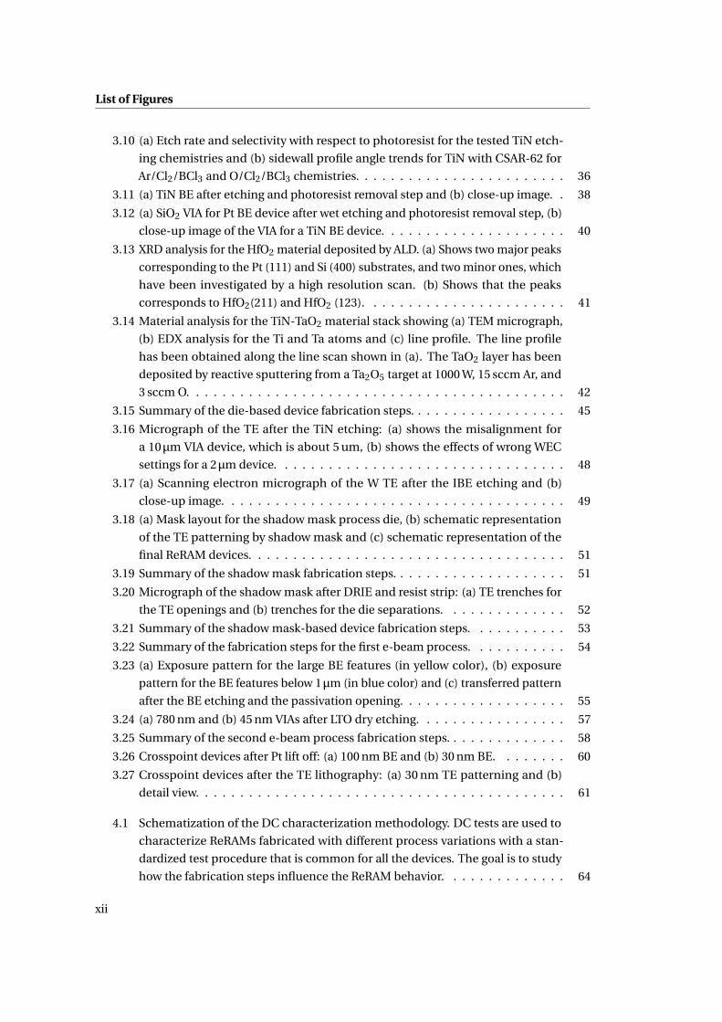
4.2 Schematic representation of the process variations analyzed with the DC tests. 65
4.3 Schematic representation of the measured quantities for the DC tests. . . . . . 65
4.4 DC electrical results for Pt/HfO2 (5 nm)/Ti (3 nm)/TiN, with SiN passivation
and IBE for the TE definition: (a) I-V curve, (b) R-V curve, (c) cycle-to-cycle
resistance, (d) relative frequency and (e) cumulative probability of the resistance
states, relative frequency for the (f) set and (g) reset voltages, (h) set voltage
versus reset voltage plot. . . . . . . . . . . . . . . . . . . . . . . . . . . . . . . . . . 69
4.5 DC electrical results in current mode for Pt/HfO2 (5 nm)/Ti (3 nm)/TiN, with
SiN passivation and IBE for the TE definition: (a) I-V curve, (b) R-V curve, (c)
cycle-to-cycle resistance, (d) cumulative probability of the resistance states. . . 71
4.6 Process type influence on the electrical characteristics of Pt/HfO2 (5 nm)/Hf
(3 nm)/TiN devices: the boxplots show (a) the forming voltage, (b) the resistance
state and (c) the switching voltage measurements. . . . . . . . . . . . . . . . . . 74
4.7 Results for Pt/HfO2 (5 nm)/TiN devices devices fabricated with the e-beam
process: (a) 800 nm VIA and (b) 45 nm VIA diameter device. . . . . . . . . . . . . 75
4.8 Resistive material influence on the electrical characteristics of Pt/x/Hf (3 nm)/TiN,
Pt/x/TiN, TiN/x/TiN and Pt/x/Ti (3 nm)/TiN devices. The boxplot shows (a) the
forming voltage, (b) the resistance state and (c) the switching voltage measure-
ments. . . . . . . . . . . . . . . . . . . . . . . . . . . . . . . . . . . . . . . . . . . . 77
4.9 Buffer layer influence on the electrical characteristics of Pt/HfO2 (3 nm)/x/TiN
and Pt/HfO2 (5 nm)/x/TiN devices. (a) Shows the device representative DC
cycles; while the boxplots show (b) the forming voltage, (c) the resistance state
and (d) the switching voltage measurements. . . . . . . . . . . . . . . . . . . . . 79
4.10 Passivation influence on the electrical characteristics of Pt/HfO2 (5 nm)/TiN
and Pt/HfO2 (5 nm)/Ti (3 nm)/TiN devices. The boxplots show (a) the forming
voltage, (b) the resistance state and (c) the switching voltage measurements. . . 81
4.11 Top electrode etching influence on the electrical characteristics of Pt/HfO2
(5 nm)/TiN, Pt/HfO2 (5 nm)/Hf (3 nm)/TiN and Pt/HfO2 (5 nm)/Ti (3 nm)/TiN
devices. The boxplots show (a) the forming voltage, (b) the resistance state and
(c) the switching voltage measurements. . . . . . . . . . . . . . . . . . . . . . . . 83
4.12 Annealing influence on the electrical characteristics of Pt/HfO2 (5 nm)/Hf (3 nm)/TiN
devices. (a) Shows the device representative DC cycles; while the boxplots show
(b) the forming voltage, (c) the resistance state and (d) the switching voltage
measurements. . . . . . . . . . . . . . . . . . . . . . . . . . . . . . . . . . . . . . . 85
4.13 VIA size influence on the electrical characteristics of Pt/HfO2 (5 nm)/Hf (3 nm)/TiN
devices with IBE TE etching. The boxplots show (a) the forming voltage, (b) the
resistance state and (c) the switching voltage measurements. . . . . . . . . . . . 87
4.14 Correlation analysis between forming, set and reset voltages for all the fabri-
cated ReRAM cells. The diagonal elements show the density plots obtained
from the data distribution. The lower elements are the scatterplot matrix plots
between forming, set and reset, while the upper elements report the correlation
coefficient values. . . . . . . . . . . . . . . . . . . . . . . . . . . . . . . . . . . . . . 91
xiii

List of Figures
4.15 Correlation analysis between forming, set and reset voltages for the HfO2 (5 nm)
fabricated ReRAM cells. The diagonal elements show the density plots obtained
from the data distribution. The lower elements are the scatterplot matrix plots
between forming, set and reset, while the upper elements report the correlation
coefficient values. . . . . . . . . . . . . . . . . . . . . . . . . . . . . . . . . . . . . . 92
4.16 Cycle-to-cycle relation for set and reset voltage of a Pt/HfO2 (5 nm)/Ti (3 nm)/TiN
cell with Si3N4 passivation. The bottom right data point shows the forming and
the first reset. . . . . . . . . . . . . . . . . . . . . . . . . . . . . . . . . . . . . . . . 94
4.17 Scatterplot of (a) LRS - reset voltage and (b) LRS - reset current for HfO2 (5 nm)-
based ReRAMs. . . . . . . . . . . . . . . . . . . . . . . . . . . . . . . . . . . . . . . 95
4.18 Correlation analysis between forming, set, reset, LRS and HRS for (a) all the
fabricated cells and (b) the HfO2 (5 nm) based ReRAMs. . . . . . . . . . . . . . . 96
4.19 Correlation analysis between all the measured electrical characteristics for all
the fabricated ReRAM cells. . . . . . . . . . . . . . . . . . . . . . . . . . . . . . . . 98
4.20 Correlation analysis between all the measured electrical characteristics for the
HfO2 (5 nm) ReRAM cells. . . . . . . . . . . . . . . . . . . . . . . . . . . . . . . . . 99
4.21 (a) HRS, (b) LRS and (c) LRS at 85˚ C retention tests for Pt/HfO2 (5 nm)/TiN devices.100
5.1 Schematization of the pulse characterization methodology. Pulse tests are used
to characterize ReRAMs fabricated from a fixed process flow with pulses with
different electrical characteristics. The goal is to study how the test parameters
influence the ReRAM behavior. . . . . . . . . . . . . . . . . . . . . . . . . . . . . . 106
5.2 Schematic representation of (a) pulse test setup and (b) characterization param-
eters varied during the pulse tests. . . . . . . . . . . . . . . . . . . . . . . . . . . . 107
5.3 Representation of the measured quantities for the pulse tests. . . . . . . . . . . 109
5.4 Scatterplot matrix showing the input domain for the pulse test parameters.
The quantities varied during the analysis are the reset voltage, set voltage, gate
voltage, pulse width and pulse slope. The diagonal elements show the density
plots obtained from the data distribution, while the lower elements are the
scatterplot between the modified quantities. The x-axis is common for all the
plots on the same column, while the y-axis is in common for all the plots in the
same row. . . . . . . . . . . . . . . . . . . . . . . . . . . . . . . . . . . . . . . . . . . 110
5.5 Scatterplot between the LRS and HRS obtained from the pulse analysis. The
figure shows that is not possible to obtain all the possible resistance configurations.111
5.6 Example of speed and retention tests for Pt/HfO2 (5 nm)/Ti (3 nm)/TiN devices:
(a) 30 ns write pulse and (b) 50 k cycles. . . . . . . . . . . . . . . . . . . . . . . . . 112
5.7 Example of pulse distortion for sub-50 ns inputs: (a) 50 ns and (b) 20 ns write
pulse. . . . . . . . . . . . . . . . . . . . . . . . . . . . . . . . . . . . . . . . . . . . . 113
5.8 Current transient behavior for Pt/HfO2 (5 nm)/Hf (3 nm)/TiN ReRAM devices.
The current is measured from the voltage drop of a series 1 kΩ resistor. The test
conditions are 1.15 V set voltage, −2.25 V reset, 1.9 V gate, 1 ms pulse width and
20% slope. . . . . . . . . . . . . . . . . . . . . . . . . . . . . . . . . . . . . . . . . . 114
xiv
List of Figures
5.9 Representation of the BER for input pulses with width larger that 800 ns and a
slope of 20%: (a) 3D scatterplot of the BER with respect to set, reset and gate
voltage, (b) 2D scatterplot of the LRS BER and (c) the HRS BER with respect to
reset and gate voltage. . . . . . . . . . . . . . . . . . . . . . . . . . . . . . . . . . . 116
5.10 Representation of the BER for input with gate voltage of 1.9 V and a slope of 20%:
(a) 3D scatterplot of the BER with respect to set, reset voltage and pulse width, (b)
2D scatterplot of the LRS BER and (c) the HRS BER with respect to reset voltage
and pulse width. . . . . . . . . . . . . . . . . . . . . . . . . . . . . . . . . . . . . . . 118
5.11 Scatterplot matrix showing the relation between the input test parameters and
the LRS BER. The quantities varied during the analysis are the reset voltage, set
voltage, gate voltage, pulse width and pulse slope. The x-axis is common for all
the plots on the same column, while the y-axis is in common for all the plots in
the same row. . . . . . . . . . . . . . . . . . . . . . . . . . . . . . . . . . . . . . . . 119
5.12 Scatterplot matrix showing the relation between the input test parameters and
the HRS BER. The quantities varied during the analysis are the reset voltage, set
voltage, gate voltage, pulse width and pulse slope. The x-axis is common for all
the plots on the same column, while the y-axis is in common for all the plots in
the same row. . . . . . . . . . . . . . . . . . . . . . . . . . . . . . . . . . . . . . . . 120
5.13 Influence of the set and reset pulse voltages on the memory resistance states
with 1.9 V gate voltage, 10μs pulse and 20% slope. (a) Resistance states obtained
by changing the reset pulse level every 2 k cycles from −1.95 V to −1.5 V, and the
set pulse level, color coded in the image, every 500 cycles from 1.5 V to 1.15 V.
(b) HRS cumulative resistance probability plot for different reset voltage values,
while the set voltage pulse is fixed at 1.38 V. (c) Modulation of the LRS with a
reset pulse voltage of −1.8 V . . . . . . . . . . . . . . . . . . . . . . . . . . . . . . . 123
5.14 Influence of the pulse width and reset voltages on the memory resistance states
with 1.35 V set pulse, 1.9 V gate voltage and 20% slope. The reset pulse level
changes every 3 k cycles from 800μs to 10μs, while the reset pulse, color coded
in the image, varies every 500 cycles from −1.55 V to −1.95 V. . . . . . . . . . . . 124
5.15 Influence of the gate and set voltages on the memory resistance states with−1.8 V
reset pulse, 10μs pulse width and 20% slope. The gate voltage level changes
every 3 k cycles from 1.7 V to 1.9 V, while the set voltage, color coded in the image,
varies every 500 cycles from 1 V to 1.4 V. . . . . . . . . . . . . . . . . . . . . . . . . 125
5.16 ANOVA dot plot for the test input influence over the (a) log(LRS) and (b) log(HRS).128
5.17 ANOVA diagnostic plots for the test input influence over the log(LRS): (a) fitted
values with respect to the residuals, (b) residuals normal Q-Q plot, (c) fitted
values with respect to the standardized residuals, (d) Cook’s distance for the data
points. . . . . . . . . . . . . . . . . . . . . . . . . . . . . . . . . . . . . . . . . . . . 129
5.18 ANOVA diagnostic plots for the test input influence over the log(HRS), (a) fitted
values with respect to the residuals, (b) residuals normal Q-Q plot, (c) fitted
values with respect to the standardized residuals, (d) Cook’s distance for the data
points. . . . . . . . . . . . . . . . . . . . . . . . . . . . . . . . . . . . . . . . . . . . 130
xv

List of Figures
5.19 Calculated coefficients with 2.5% and 97.5% confidence levels for the (a) log(LRS)
and (b) log(HRS) models. . . . . . . . . . . . . . . . . . . . . . . . . . . . . . . . . 133
5.20 Diagnostic plots for the log(LRS) model: (a) fitted values with respect to the
residuals, (b) residuals normal Q-Q plot, (c) fitted values with respect to the
standardized residuals, (d) leverage with respect to the standardized residuals. 134
5.21 Diagnostic plots for the log(HRS) model: (a) fitted values with respect to the
residuals, (b) residuals normal Q-Q plot, (c) fitted values with respect to the
standardized residuals, (d) leverage with respect to the standardized residuals. 135
5.22 Example of pulse number resistance modulation. The reset pulses have 1μs
width, 20% slope, a period of 100 ms and a width of (a) −1.15 V and (b) −1 V. . . 137
6.1 Schematic representation of the sneak-path current. The total current has two
components: one is the current flowing through the selected device, in blue in
the figure, and one resulting from the unselected memory components in a LRS. 141
6.2 I-V curve measurement for the fabricated TiN/TaO2 (25 nm)/TiN ReRAM cells
and Verilog-A model. . . . . . . . . . . . . . . . . . . . . . . . . . . . . . . . . . . . 142
6.3 Read/Write circuit block diagram. The system is composed by row and column
drivers, a digital controller and a reference voltage generator. . . . . . . . . . . . 144
6.4 Schematic representation of (a) the row driver and (b) the column driver. . . . . 145
6.5 Chip micrograph. The systems includes different size of ReRAM arrays (up to
128×8), a read/write circuitry and single cell test areas. . . . . . . . . . . . . . . . 146
6.6 Post layout simulation of the voltage drop across an unselected ReRAM cell
(a) with and (b) without the calibration circuit during the read operation. The
voltage difference between the column (blue) and row (red) voltages, directly
proportional to the cell sneak-path current, is reduced by more than one order
of magnitude when the calibration circuit is active. . . . . . . . . . . . . . . . . . 147
6.7 Representative I-V characteristic for ReRAM, threshold type selector and 1S1R
device (adapted from [29]). . . . . . . . . . . . . . . . . . . . . . . . . . . . . . . . 148
6.8 DC characteristics for the Pt/VO2/Pt selector devices. (a) Shows the represen-
tative DC cycles; while the boxplots show (b) the resistance state and (c) the
switching voltage measurements. . . . . . . . . . . . . . . . . . . . . . . . . . . . 154
6.9 I-V characteristic for the 1S1R device stack. The Pt/VO2/Pt selector is in series
with the Pt/HfO2 (5 nm)/Ti (3 nm)/TiN ReRAM. . . . . . . . . . . . . . . . . . . . 155
6.10 (a) Scanning electron micrograph of the MMC capacitor and (b) FIB-SEM cross
section. . . . . . . . . . . . . . . . . . . . . . . . . . . . . . . . . . . . . . . . . . . . 156
6.11 Process flow representation for the carrier wafer fabrication: (a) Si substrate, (b)
Si DRIE, (c) chip mounting, (d) parylene deposition, (e) photolithography, (f)
parylene RIE. . . . . . . . . . . . . . . . . . . . . . . . . . . . . . . . . . . . . . . . 157
6.12 Micrograph of the carrier wafer with embedded the CMOS chip. The visible
notch is used to facilitate the chip release. . . . . . . . . . . . . . . . . . . . . . . 157
xvi
List of Figures
6.13 Process flow representation for ReRAM post-processing: (a) parylene layer coat-
ing, (b) photolithography, (c) parylene RIE, (d) passivation BHF, (e) TaOx sputter-
ing, (f) parylene lift off. . . . . . . . . . . . . . . . . . . . . . . . . . . . . . . . . . . 158
6.14 Scanning electron micrograph of an 8 Bit line-8 Word line crossbar array with
Word and Bit lines in M6 and M5. Inset shows a TEM cross section of the memory
cross point. One of the ReRAM cells is highlighted in yellow. . . . . . . . . . . . . 159
6.15 Transmission electron micrograph of the MMC-M5 interface. (a) Bright field
image and (b) EDX elemental analysis. . . . . . . . . . . . . . . . . . . . . . . . . 159
6.16 Electrical results for the TiN/TaO2/TiN ReRAM integrated cell. Set voltage is
−1 V, Reset voltage is 1.3 V. The operating voltages are compatible for low-voltage
applications. . . . . . . . . . . . . . . . . . . . . . . . . . . . . . . . . . . . . . . . . 160
6.17 (a) Micrograph of the 2×2 ReRAM array integrated on the chip. (b) I-V curve of
the TiN/TaOTaOx/TiN integrated ReRAM. . . . . . . . . . . . . . . . . . . . . . . . 162
A.1 Setup for the (a) DC and (b) pulse measurements. . . . . . . . . . . . . . . . . . . 170
A.2 (a) Pulse measurement procedure and (b) single pulse parameters. . . . . . . . 171
A.3 Oscilloscope data of a 50Ω resistor in series to TiN/TaO2 (25 nm)/TiN ReRAM
cell during the forming operation: the parameter analyzer 500μA current com-
pliance is reached just after 70μs and with a peak current of 1.2 mA. . . . . . . . 172
A.4 DC data analysis example: (a) I-V curve, (b) R-V curve, (c) cycle-to-cycle resis-
tance, (d) relative frequency and (e) cumulative probability of the resistance
states, relative frequency for the (f) set and (g) reset voltages, (h) set voltage
versus reset voltage plot. . . . . . . . . . . . . . . . . . . . . . . . . . . . . . . . . . 174
A.5 Pulse data analysis example. . . . . . . . . . . . . . . . . . . . . . . . . . . . . . . 175
A.6 ANOVA diagnostic plot example: (a) fitted values with respect to the residuals,
(b) residuals normal Q-Q plot, (c) fitted values with respect to the standardized
residuals, (d) Cook’s distance for the data points. . . . . . . . . . . . . . . . . . . 181
A.7 ANOVA plot example: (a) fitted values with respect to the residuals, (b) residuals
normal Q-Q plot, (c) fitted values with respect to the standardized residuals, (d)
Cook’s distance for the data points. . . . . . . . . . . . . . . . . . . . . . . . . . . 182
xvii


List of Tables2.1 Number of particles per bit for memory technologies (adapted from [4]). . . . . 9
2.2 Emerging memory products. . . . . . . . . . . . . . . . . . . . . . . . . . . . . . . 10
2.3 Energy efficiency for memory technologies (adapted from [4]). . . . . . . . . . . 12
2.4 Barrier heights for memory technologies (adapted from [4]). . . . . . . . . . . . 13
2.5 Switching time for memory technologies (adapted from [4]). . . . . . . . . . . . 15
2.6 Device characteristics of mainstream and emerging memory technologies [12]. 15
3.1 Investigated recipes for TiN dry plasma etching. . . . . . . . . . . . . . . . . . . . 33
3.2 TaOx compositions. . . . . . . . . . . . . . . . . . . . . . . . . . . . . . . . . . . . . 41
4.1 Process variations and measured quantities during the DC tests. . . . . . . . . . 65
4.2 Process variations. . . . . . . . . . . . . . . . . . . . . . . . . . . . . . . . . . . . . 68
4.3 Summary of the DC electrical characteristics for Pt/HfO2 (5 nm)/TiN devices
fabricated with die and ebeam process. . . . . . . . . . . . . . . . . . . . . . . . . 75
5.1 Test variations and measured quantities for the pulse tests. . . . . . . . . . . . . 108
5.2 ANOVA table for the test input influence over the log(LRS). . . . . . . . . . . . . 127
5.3 ANOVA table for the test input influence over the log(HRS). . . . . . . . . . . . . 127
5.4 Regression model summary for the LRS. . . . . . . . . . . . . . . . . . . . . . . . 131
5.5 Regression model summary for the log(LRS). . . . . . . . . . . . . . . . . . . . . . 132
5.6 Regression model summary for the log(HRS). . . . . . . . . . . . . . . . . . . . . 132
6.1 Verilog-A model fitting parameters. . . . . . . . . . . . . . . . . . . . . . . . . . . 143
7.1 Summary and comparison of the fabricated device performances. . . . . . . . . 166
A.1 Example of a regression model summary. . . . . . . . . . . . . . . . . . . . . . . . 183
xix


List of Acronyms
AES Auger Electron Spectroscopy
AFM Atomic Force Microscope
ALD Atomic Layer Deposition
ANOVA Analysis of Variance
BE Bottom Electrode
BEoL Back End of the Line
BER Bit Error Ratio
BHF Buffered Hydrofluoric Acid
CMI Center of MicroNanoTechnology of EPFL
CMOS Complementary Metal Oxide Semiconductor
DRAM Dynamic Random Access Memory
DRIE Deep Reactive Ion Etching
EBR Edge Bead Removal
EDX Energy-Dispersive X-Ray Spectroscopy
FeRAM Ferroelectric Random Access Memory
FIB Focused Ion Beam
HRS High Resistance State
IBE Ion Beam Etching
LER Line Edge Roughness
LPCVD Low Pressure Chemical Vapor Deposition
xxi

List of Acronyms
LRS Low Resistance State
LTO Low Temperature Oxide
MIEC Mixed Ionic Electronic Conduction
MIT Metal-Insulator Transition
MMC Metal to Metal Capacitor
MRAM Magnetoresistive Random Access Memory
NVM Non Volatile Memory
OTS Ovonic Threshold Switch
OxRAM Oxide-Based Random Access Memory
PAM Pre Alignment Marker
PCRAM Phase Change Random Access Memory
PEC Proximity Effect Correction
PECVD Plasma Enhanced Chemical Vapor Deposition
RAM Random Access Memory
ReRAM Resistive Random Access Memory
RIE Reactive Ion Etching
RTP Rapid Thermal Processing
SEM Scanning Electron Microscope
SIMS Secondary Ions Mass Spectroscopy
SMU Source Measure Unit
SPGU Semiconductor Pulse Generator Unit
SRAM Static Random Access Memory
SRD Spin Rinse Dryer
SSD Solid-State Drive
STTRAM Spin-Transfer Torque Random Access Memory
TE Top Electrode
TEM Transmission Electron Microscope
xxii

List of Acronyms
WEC Wedge Error Compensation
XPS X-Ray Photoemission Spectroscopy
XRD X-Ray Diffraction
xxiii

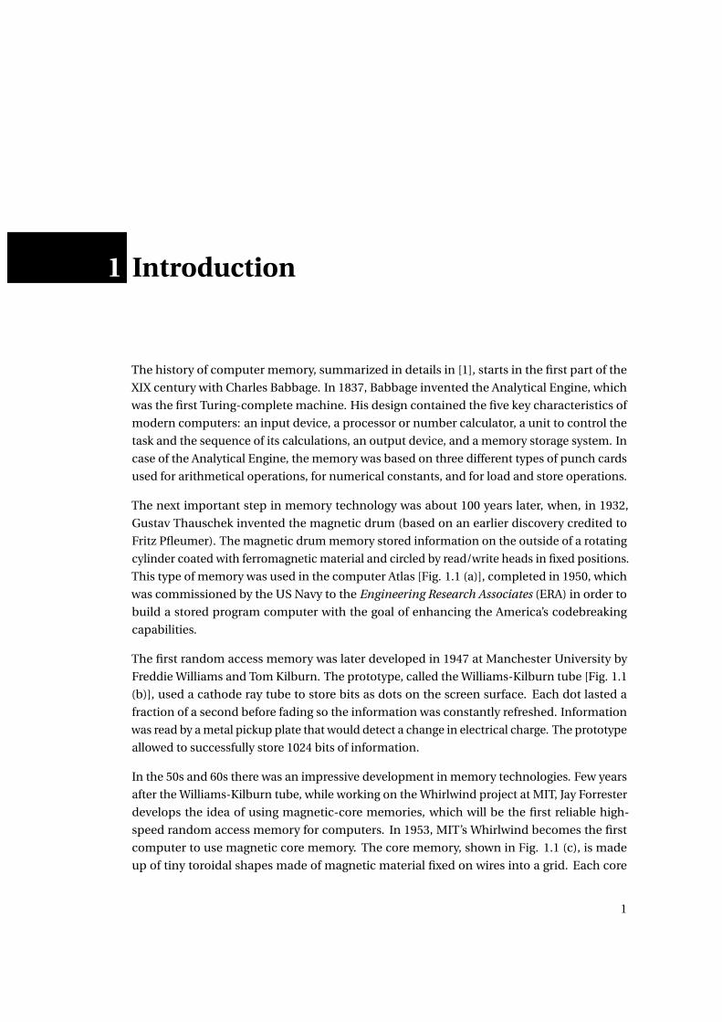
1 Introduction
The history of computer memory, summarized in details in [1], starts in the first part of the
XIX century with Charles Babbage. In 1837, Babbage invented the Analytical Engine, which
was the first Turing-complete machine. His design contained the five key characteristics of
modern computers: an input device, a processor or number calculator, a unit to control the
task and the sequence of its calculations, an output device, and a memory storage system. In
case of the Analytical Engine, the memory was based on three different types of punch cards
used for arithmetical operations, for numerical constants, and for load and store operations.
The next important step in memory technology was about 100 years later, when, in 1932,
Gustav Thauschek invented the magnetic drum (based on an earlier discovery credited to
Fritz Pfleumer). The magnetic drum memory stored information on the outside of a rotating
cylinder coated with ferromagnetic material and circled by read/write heads in fixed positions.
This type of memory was used in the computer Atlas [Fig. 1.1 (a)], completed in 1950, which
was commissioned by the US Navy to the Engineering Research Associates (ERA) in order to
build a stored program computer with the goal of enhancing the America’s codebreaking
capabilities.
The first random access memory was later developed in 1947 at Manchester University by
Freddie Williams and Tom Kilburn. The prototype, called the Williams-Kilburn tube [Fig. 1.1
(b)], used a cathode ray tube to store bits as dots on the screen surface. Each dot lasted a
fraction of a second before fading so the information was constantly refreshed. Information
was read by a metal pickup plate that would detect a change in electrical charge. The prototype
allowed to successfully store 1024 bits of information.
In the 50s and 60s there was an impressive development in memory technologies. Few years
after the Williams-Kilburn tube, while working on the Whirlwind project at MIT, Jay Forrester
develops the idea of using magnetic-core memories, which will be the first reliable high-
speed random access memory for computers. In 1953, MIT’s Whirlwind becomes the first
computer to use magnetic core memory. The core memory, shown in Fig. 1.1 (c), is made
up of tiny toroidal shapes made of magnetic material fixed on wires into a grid. Each core
1
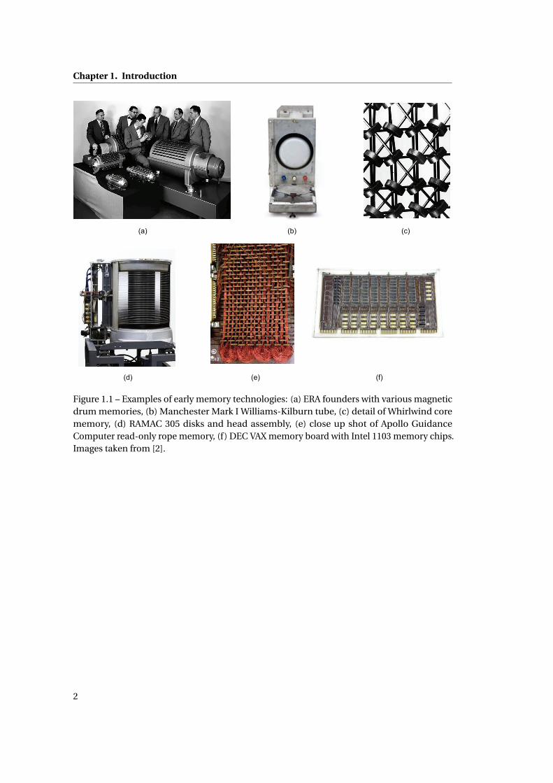
Chapter 1. Introduction
Figure 1.1 – Examples of early memory technologies: (a) ERA founders with various magneticdrum memories, (b) Manchester Mark I Williams-Kilburn tube, (c) detail of Whirlwind corememory, (d) RAMAC 305 disks and head assembly, (e) close up shot of Apollo GuidanceComputer read-only rope memory, (f) DEC VAX memory board with Intel 1103 memory chips.Images taken from [2].
2

stored a bit, magnetized one way for a “zero,” and the other way for a “one.” The wires could
both detect and change the state of a bit. Magnetic core memory was widely used as the
main memory technology for computers well into the 1970s, when Intel introduced the 1103
Dynamic Random Access Memory (DRAM) integrated circuit, which signaled the beginning of
the end for magnetic core memory in computers.
Few years later, the era of magnetic disk storage dawns in 1956 with IBM’s RAMAC 305 com-
puter system. The computer was based on the new technology of the hard disk drive. The
RAMAC disk drive [Fig. 1.1 (d)] consisted of 50 magnetically coated metal platters capable
of storing about 5 million characters of data. RAMAC allowed real-time random access to
large amounts of data, unlike magnetic tape or punched cards. A working RAMAC hard disk
assembly is still demonstrated regularly at the Computer History Museum in Mountain View
(California).
When Bell Labs introduces in 1955 its first transistor computer revolutionizing electronics,
memories were affected as well. Transistors are indeed faster, smaller, and create less heat
than traditional vacuum tubs, making these computers more reliable and efficient. In 1964,
John Schmidt designs a 64-bit MOS p-channel Static RAM while at Fairchild, and later, the
1966 issue of Electronics magazine features an 8-bit RAM designed by Signetics for the SDS
Sigma 7 mainframe computer. The article, titled “Integrated scratch pads sire new generation
of computers” [3], describes one of the earliest uses of dedicated semiconductor memory
devices in computer systems.
In the same years, a very interesting memory prototype is the read-only rope memory used
in the Apollo Guidance Computer [Fig. 1.1 (e)]. This was launched into space aboard the
Apollo 11 mission in 1969, which carried American astronauts to the Moon and back. This
rope memory was made by hand, and was equivalent to 72 KB of storage. Manufacturing rope
memory was laborious and slow, and it could take months to weave a program into the rope
memory. If a wire went through one of the circular cores it represented a binary one, and those
that went around a core represented a binary zero.
The next breakthrough in memory technology was in 1968, when Robert Dennard at the IBM
T.J. Watson Research center is granted a U.S. patent describing a one-transistor DRAM cell. In
1970, the introduction of the 1 kb Intel 1103 memory chip [Fig. 1.1 (f)] marks the beginning
of the end for magnetic core memory and ushers in the era of DRAM integrated circuits for
main memory in computers. The 1103 sold slowly at first, however, at a price of 1 cent per bit
and with a speed compatible with existing logic circuits, sales skyrocketed after several design
revisions.
As sales soared when DRAMs entered commercial production in the early 1970s, the Japanese
Trade Ministry sees a chance to make Japan a leader in the DRAM chip industry. With customer
demand in the millions, DRAMs became the first mass market chip, sparking fierce interna-
tional competition. In 1976, the Japanese Trade Ministry funded Fujitsu, Hitachi, Mitsubishi,
NEC, and Toshiba to develop 64 k DRAMs. The consortium triumphed, decimating American
3
Chapter 1. Introduction
memory suppliers and provoking the U.S. government to threaten trade sanctions. Although
tensions eased between Japanese and American manufacturers, Korea soon overtook them
both.
Flash memory was later invented in 1984 by Fujio Masuoka while working for Toshiba. Capable
of being erased and re-programmed multiple times, Flash memory quickly gained a loyal
following in the computer memory industry. Although Masuoka’s idea won praise, he quickly
left Toshiba to become a professor at Tohoku University. Later, a Flash-based prototype Solid
State Disk (SSD) module is made for evaluation by IBM in 1992. SanDisk, which at time
was known as SunDisk, manufactured the module which used non-volatile memory chips to
replace the spinning disks of a hard disk drive. SanDisk recognized that hand-held devices
and computers were becoming lighter and smaller, and that Flash memory offered powerful
advantages over hard disks. Next, in 2000, USB Flash drives are introduced. Sometimes
referred to as jump drives or memory sticks, these drives consisted of Flash memory encased
in a small form factor container with a USB interface. They could be used for data storage and
in the backing up and transferring of files between various devices. They were faster and had
greater data capacity than earlier storage media. Also, they could not be scratched like optical
discs and were resilient to magnetic erasure, unlike floppy disks. Drives for floppy disks and
optical discs faded in popularity for desktop PCs and laptops in favor of USB ports after Flash
drives were introduced.
In the last years, the technological evolution continued by the investigation of new types of
memory devices, which are also referred as emerging memory technologies. Among these
technologies there are Resistive Random Access Memory (ReRAM) devices, which are the main
subject of this dissertation.
1.1 Thesis goal
This thesis focuses on the development of ReRAM devices. The main subject is the qualitative
and quantitative description of the main factors that influence the resistive memory elec-
trical behavior. Such factors can be related either to the memory fabrication or to the test
environment.
The first category includes variations in the fabrication process steps, in the device geometry
or composition. The second one describes how differences in the electrical stimuli sent to
the device change the memory performances. The results obtained through this analysis are
tailored not only for standard memory applications, but also for new memory paradigms, such
as non-Von Neumann architectures.
The second subject of this work is the integration of the fabricated devices in a Complementary
Metal Oxide Semiconductor (CMOS) technology environment. As discussed in this thesis, this
includes the modeling of the fabricated devices and their integration on the back end of the
line of a CMOS chip. Furthermore, we show auxiliary devices, i.e., selectors, that can be used
4
1.2. Thesis overview
in order to improve the ReRAM performances for high-density configurations.
1.2 Thesis overview
Chapter 2: ReRAM introduction
In Chapter 2, we give an overview of the mainstream memory technologies and the reasons that
lead to the study of alternative device solutions. This will be followed by a comparison between
the emerging technologies with respect to the mainstream memories, first by considering
their different working mechanisms, then by comparing the state-of-the-art performances.
The final part of the chapter focuses on ReRAMs. We review the device taxonomy, structure,
switching mechanism and available models. This chapter presents the basic information
needed for the remainder of the document.
Chapter 3 - Device fabrication
In Chapter 3, we describe the ReRAMs fabrication processes. We present the adopted process
flows in details, describing every fabrication step, as well as the process development and the
material characterization of the fabricated devices.
Chapter 4 - Device characterization: DC analysis
Chapter 4 provides the electrical data obtained for DC tests. The goal of the analysis is to
show how different process flow variations and device compositions reflect on the memory
electrical characteristics, and to gather insights about the ReRAM working mechanism and
the adopted methodology approach. First, we present the factors analyzed during this study.
We then present some examples from the measured data, obtained either by forcing a voltage
or a current into the device. Next, we highlight and discuss the influence of each specific fabri-
cation process variation over the obtained memory characteristics. Afterwards, we perform a
correlation analysis on the result database, analyzing the features that are common among all
the fabricated devices, regardless of the process differences. The target is to highlight the rela-
tions that are intrinsic for ReRAM devices, and to validate the characterization methodology.
Finally, we conclude with the results obtained from retention tests.
Chapter 5 - Device characterization: pulse analysis
Chapter 5 shows the electrical data obtained for pulse tests. The goal of this analysis is to show
how the test conditions can modify the device behavior. First, we describe the factors analyzed
during the experiments. Then, we present some examples from the measurement data, such as
endurance and write speed tests. Next, we report the failure analysis of the fabricated devices,
which discusses the correct test parameters for the memories. We subsequently discuss the
5

Chapter 1. Introduction
influence of the test conditions on the ReRAM characteristics, and we propose an empirical
model to describe such changes. Finally, we show how it is possible to control the memory
resistance state by modulating the number of input pulses.
Chapter 6 - CMOS system integration
Chapter 6 describes the integration of the fabricated resistive memories within standard
CMOS technology. The intent is to obtain a hybrid ReRAM-CMOS system in a passive crossbar
array configuration. We first start by introducing the main memory arrangements and the
sneak-path current issue. Then, we show a Verilog-A model used to simulate the device
electrical behavior. Subsequently, we present a CMOS read circuit implementation to reduce
the sneak-current path in passive crossbar memory arrays. Next, we discuss the fabrication
and characterization of selector devices. Finally, we show two methods to integrate resistive
memories in the back end of the line of CMOS chips.
Chapter 7 - Conclusion and future work
The conclusion of the work is presented in Chapter 7. The main results and the contributions
of this work are summarized in this chapter, and a perspective on future works is given.
6
2 ReRAM introduction
In this chapter, we first give an overview of the mainstream memory technologies and the
reasons that lead to the study of alternative device solutions in Section 2.1. This will follow by
a comparison between the emerging technologies with respect to the mainstream memories,
first by considering their different working mechanisms, then by comparing the state-of-the-
art performances in Section 2.2. The final part of the chapter, presented in Section 2.3, focuses
on Resistive Random Access Memories. We review the device taxonomy, structure, switching
mechanism and available models.
2.1 Memory technology overview
The functionalities and performances of today’s computing systems are increasingly depen-
dent on the memory block. This phenomenon, also referred as the Von Neumann bottleneck,
is the main motivation for the research on memory technologies. The memory subsystem is
classically arranged in a hierarchy with several different levels. The top level is occupied by
Static Random Access Memories (SRAMs), serving as cache. The step below in the hierarchy is
taken by Dynamic Random Access Memories (DRAMs), which are used as the main memory of
a computer system. One level below there is Flash memory, which is the technology used for
Solid-State Drive (SSD) memory. The two main types of Flash memory are named NAND and
NOR, as the cells exhibit internal characteristics similar to the corresponding gates. Finally,
in older systems, magnetic memory constitute the hard drive mass storage. Moving down
the hierarchy, the cost per bit decreases and the memory capacity increases. On the contrary,
moving up the hierarchy, the speed of the devices increases.
All the mainstream technologies described above (SRAM, DRAM, Flash) are based on charge
storage mechanisms. In SRAMs, the charge is stored at the nodes between two cross-coupled
inverters. In DRAMs, the charge is accumulated on the cell capacitor, while for Flash technol-
ogy the charges are trapped in the floating gate. All these charge-based memories are facing
challenges to be scaled below the 10 nm technology node due to the easy loss of the stored
charge. This results in a degradation of the memory performance, reliability and noise margin.
7
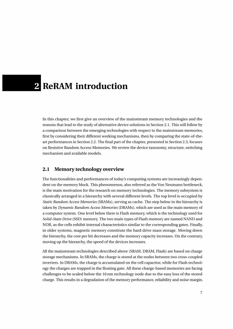
Chapter 2. ReRAM introduction
Figure 2.1 – Charge based memories: (a) evolution of electrons required per level in NANDtechnology (adapted from [4]) and (b) capacitor trenches in IBM Power 7+ e-DRAM (32 nm)[5].
An example of the charge needed per memory level in NAND Flash memories is reported in
Fig. 2.1 (a), where it can be seen that for the planar 16 nm technology node, each bit level
requires approximately only 16 electrons. In DRAM the main challenge is the creation of
capacitors with high enough capacitance to store the charge. With the reduction of the space
in the lateral dimension, due to the technology progress, the only possibility is using deeper
and deeper trenches to store the charge. This solution, due to the requirement of an extremely
high etching aspect ratio, is not applicable for deeply scales technology nodes. An example of
the capacitor trenches for embedded DRAM cells in the IBM power 7+ processor is shown in
Fig. 2.1 (b). Moreover, SRAM is inherently difficult to be scaled down because it is generally
composed by six transistors.
The main motivation for the development of emerging Non Volatile Memories (NVMs) is
the study of a different mechanism to store the digital state in order to overcome the chal-
lenges that the mainstream memories are facing for scaled nodes. Among these emerging
technologies, the ones that seem more promising are Phase Change Memories (PCRAMs), Re-
sistive Random Access Memories (ReRAMs) and Spin-Transfer Torque Random Access Memories
(STTRAMs). These memory technologies are two terminal devices, and the information is
stored by different defined resistance states. In PCRAM, information is stored as a result of
the resistance difference between the crystalline and the amorphous phase of a chalcogenide
material. ReRAM switching mechanism is based on the formation or rupture of a conduc-
tive filament inside a dielectric layer. STTRAM relies on the difference between parallel and
anti-parallel configuration of two ferromagnetic layers separated by a thin tunneling insulator
layer. An estimation of the number of particles required to store one bit of information for the
different memory technologies is reported in Table 2.1. For the same cell volume, the emerging
NVMs have a number of particle several order of magnitude higher than NAND Flash. The
main incentive for emerging NVM development is to have a high number of particles paired
8
2.2. Emerging memory technologies
Technology Memory mechanism Fundamental particleParticles in a 20 nmcell
DRAMElectrons stored in acapacitor
Electron ~105 (∗)
NANDElectrons stored in afloating gate
Electron ~50/state
PCRAMCrystalline state, amor-phous state
Atomic bond, bond an-gle, bond configura-tion, Ge octaedral/te-tragonal coordination
~5×10⁴
ReRAMConductive filament,broken filament
Cu ions or oxygen va-cancies
10-1000
STTRAMCorrelated electronspins (Bohr mag-netrons)
Bohr magnetron ~4×10⁴ (∗∗)
(∗) 25 fF×0.6 V.(∗∗) 20 nm diameter × 2 nm thick free layer, 2μb/Co, Fe atom.
Table 2.1 – Number of particles per bit for memory technologies (adapted from [4]).
with the low pitch resulting from the two terminal structure.
In earlier years, researchers in emerging memory technologies were looking for a "universal"
memory, or, in other words, a memory device that could serve as a replacement for SRAM,
DRAM and Flash. The desired characteristics for such technology would be a fast read/write
speed (< ns), low operating voltage (< 1 V), low energy consumption (~ fJ/bit), long data
retention (> 10 years), long write and read endurance (> 107 cycles) and excellent scalability
(<10 nm). With time, it becomes clear that a device with such characteristics may not exist,
even thought emerging memory technologies were able to satisfy part of the ideal charac-
teristics listed above. Today, beside trying to be the replacement for one of the mainstream
memories, emerging devices have the potential to change the current memory hierarchy by
adding one or more levels. For example, IBM proposed to use these technologies to create
a "storage class" memory cathegory [6], i.e., a level in between the main memory and the
storage memory.
2.2 Emerging memory technologies
Today’s commercial products based on emerging memories are mostly limited to niche mar-
kets with a relatively low density. A list of the main companies and products is reported
in Table 2.2. In the table, the acronym MRAM stands for Magnetoresistive Random Access
Memory, which is an predecessor of STTRAM, while FeRAM stands for Ferroelectric Random
Access Memory, a technology based on magnetic materials.
9
Chapter 2. ReRAM introduction
Technology Company Niche market
ReRAM Adesto EEPROM replacementReRAM Adesto medical - sterilization tolerant memoryReRAM Fujitsu EEPROM replacementReRAM Panasonic Smoke detectorMRAM Everspin Ultra high reliability BBSRAM replacementSTTRAM Crocus Embedded securityFeRAM TI EmbeddedFeRAM Cypress Low density - power meters
Table 2.2 – Emerging memory products.
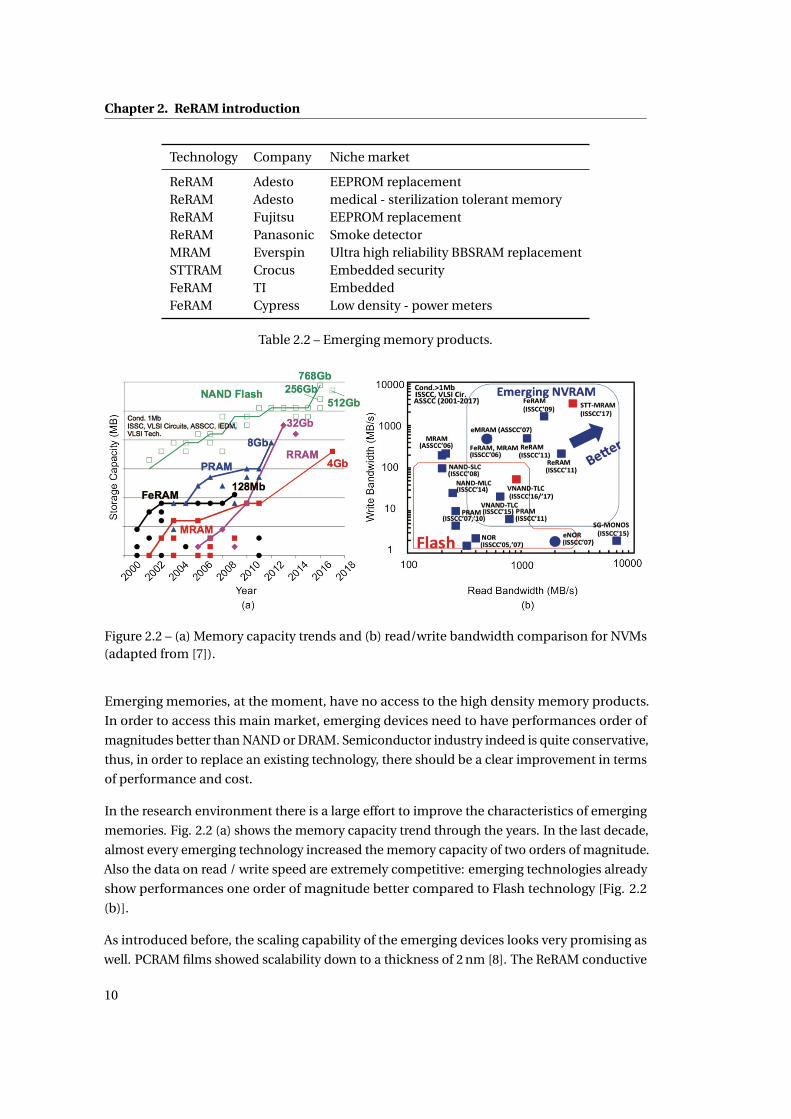
Figure 2.2 – (a) Memory capacity trends and (b) read/write bandwidth comparison for NVMs(adapted from [7]).
Emerging memories, at the moment, have no access to the high density memory products.
In order to access this main market, emerging devices need to have performances order of
magnitudes better than NAND or DRAM. Semiconductor industry indeed is quite conservative,
thus, in order to replace an existing technology, there should be a clear improvement in terms
of performance and cost.
In the research environment there is a large effort to improve the characteristics of emerging
memories. Fig. 2.2 (a) shows the memory capacity trend through the years. In the last decade,
almost every emerging technology increased the memory capacity of two orders of magnitude.
Also the data on read / write speed are extremely competitive: emerging technologies already
show performances one order of magnitude better compared to Flash technology [Fig. 2.2
(b)].
As introduced before, the scaling capability of the emerging devices looks very promising as
well. PCRAM films showed scalability down to a thickness of 2 nm [8]. The ReRAM conductive
10
2.2. Emerging memory technologies
filament has been measured to be about 5 nm wide [9], and 10 nm × 10 nm cells have been
demonstrated [10]. STTRAM devices of 20 nm have been presented as well [11].
In the next paragraphs, we attempt to make a comparison between the existing memory
technologies. This will be based on the energy efficiency, data integrity and switching time.
2.2.1 Energy efficiency
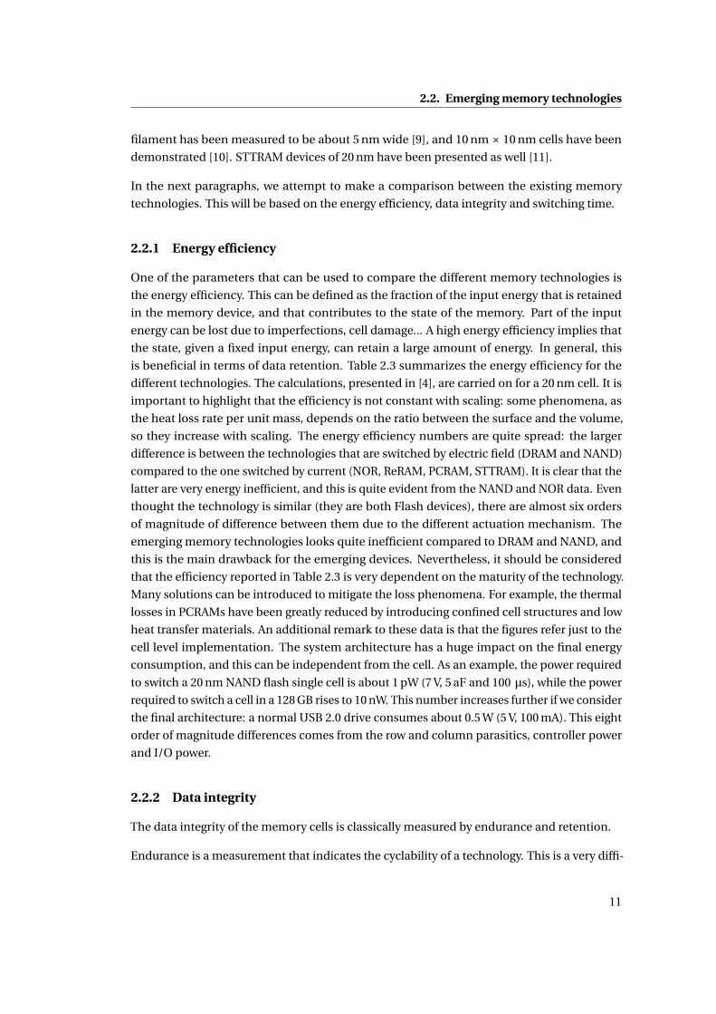
One of the parameters that can be used to compare the different memory technologies is
the energy efficiency. This can be defined as the fraction of the input energy that is retained
in the memory device, and that contributes to the state of the memory. Part of the input
energy can be lost due to imperfections, cell damage... A high energy efficiency implies that
the state, given a fixed input energy, can retain a large amount of energy. In general, this
is beneficial in terms of data retention. Table 2.3 summarizes the energy efficiency for the
different technologies. The calculations, presented in [4], are carried on for a 20 nm cell. It is
important to highlight that the efficiency is not constant with scaling: some phenomena, as
the heat loss rate per unit mass, depends on the ratio between the surface and the volume,
so they increase with scaling. The energy efficiency numbers are quite spread: the larger
difference is between the technologies that are switched by electric field (DRAM and NAND)
compared to the one switched by current (NOR, ReRAM, PCRAM, STTRAM). It is clear that the
latter are very energy inefficient, and this is quite evident from the NAND and NOR data. Even
thought the technology is similar (they are both Flash devices), there are almost six orders
of magnitude of difference between them due to the different actuation mechanism. The
emerging memory technologies looks quite inefficient compared to DRAM and NAND, and
this is the main drawback for the emerging devices. Nevertheless, it should be considered
that the efficiency reported in Table 2.3 is very dependent on the maturity of the technology.
Many solutions can be introduced to mitigate the loss phenomena. For example, the thermal
losses in PCRAMs have been greatly reduced by introducing confined cell structures and low
heat transfer materials. An additional remark to these data is that the figures refer just to the
cell level implementation. The system architecture has a huge impact on the final energy
consumption, and this can be independent from the cell. As an example, the power required
to switch a 20 nm NAND flash single cell is about 1 pW (7 V, 5 aF and 100 μs), while the power
required to switch a cell in a 128 GB rises to 10 nW. This number increases further if we consider
the final architecture: a normal USB 2.0 drive consumes about 0.5 W (5 V, 100 mA). This eight
order of magnitude differences comes from the row and column parasitics, controller power
and I/O power.
2.2.2 Data integrity
The data integrity of the memory cells is classically measured by endurance and retention.
Endurance is a measurement that indicates the cyclability of a technology. This is a very diffi-
11
Chapter 2. ReRAM introduction
TechnologyInput energy,20 nm cell
Typical inputenergy, 20 nmcell [J]
Energyefficiency
Calculationfor retentionloss
Loss mecha-nism duringwriting
DRAM
E =1/2CV 2 =1/2 × 25 f F ×(1.2V )2
1.8×10⁻¹⁴ ~1 Zero lossRelaxation, di-electric leak-age and loss
NAND E = 1/2CV 2 1×10-16 ~1 Zero loss
Electronstrapped out-side floatinggate
NOR E = I ×V × t~1×10⁻⁹
(50 nm cell)~1×10⁻⁶ E = 1/2CV 2
Very few elec-trons injectedin the floatinggate
PCRAME = I × V ×t = 100u A ×2.5V ×250ns
6.25×10⁻¹¹~1×10⁻³ (Re-set), ~1×10⁻⁵
(Set)
Phase transi-tion barrier(amorphousto crystalline2.3 eV, 5 nm)
Thermalenergy lossoutside thechalcogenite
ReRAME = I ×V × t =50u A×2.5V ×50ns
6.25×10⁻¹² ~2×10⁻³-~1.2×10⁻⁴
Activationenergy forchargedvacancy diffu-sion in HfO2,0.5 eV
Thermalenergy loss,parasiticcurrents
STTRAME = I ×V × t =40u A×0.4V ×10ns
1×10-13 ~1×10⁻⁶ 60 KT/inputenergy
Spin relatedthermalagitation,tunnellingefficiency,stochasticswitching
Table 2.3 – Energy efficiency for memory technologies (adapted from [4]).
12
2.2. Emerging memory technologies
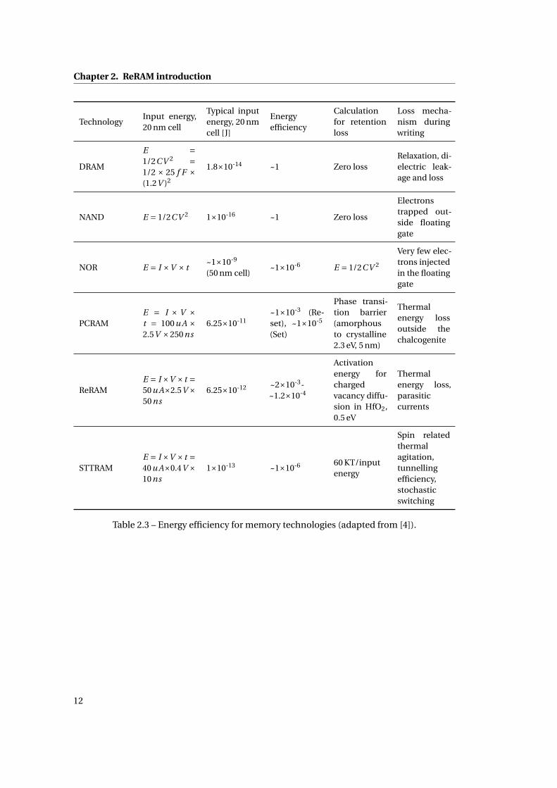
Technology Barrier between states Ea Retention limitation
DRAMMinority carriers re-combination rate
0.55 eV
Charge leakagethrough junctionof charge stored incapacitor
NAND Tunnel oxide barrier
0.1 eV stress inducedleackage current, 1 eVdetrapping, 1.2 eVthermionic emission
Charge leakagethrough tunnel oxideto neutral Vt
PCRAM
Difference in Gibbsfree energy plus ther-mal energy to reach ac-tivated state
2.4 eV Ea of GST 225
ReRAMPosition of metal oroxygen ions
1.4-1.8 eVThermal diffusionfrom ion to or fromfilament
STTRAMMagnetic anisotropyof free layer
1.55 eVRandom thermal fluc-tuations
Table 2.4 – Barrier heights for memory technologies (adapted from [4]).
cult parameter to be determined for emerging memories. Indeed, there is a huge discrepancy
between the figures reported by industry and by academic publications. For example, PCRAM
products have achieved 106 cycles, while the record for published cells is about 1013 cycles.
The endurance number that defines a product indeed requires a large volume of data (i.e., 3σ
or 6σ, where σ is the standard deviation), and it depends on the Bit Error Ratio (BER) target
and the error correction capability. Keeping this in mind, a larger endurance is one of the
advantages of the emerging memory technologies over Flash. A summary of the endurance
numbers are reported later in Table 2.6.
Retention is the ability of the memory to retain a memory state in time. It is measured in years,
and usually it is calculated from the energy stored in the cell and the energy barrier height
between states. Generally the barrier height is measured by temperature accelerated activation
energy Ea , and a high Ea is usually preferable. It should be noted that Ea is also an indication
of a device temperature sensitivity, and that retention measurements should generally include
a large volume of data. A summary of the Ea for different memory technologies is reported
in Table 2.4. As indicated before, a low Ea usually corresponds to a low retention rime. As an
example, DRAM, with a Ea of 0.55 eV, has a retention time around 50 ms. According to these
calculations, emerging memories could be as performing as mainstream memories, or even
outperform them.
Another issue worsening the data integrity is the read disturbance. The read disturbance is a
phenomena that limits the time that a read operation can be performed on a cell. This is quite
13
Chapter 2. ReRAM introduction
difficult to be predicted and it should be addressed experimentally. Every technology has its
own peculiar source of disturbance mechanism, so it is not possible to draw a comparison
between the different device types. For example, ReRAM disturbance is due to the speed of
ion drift, while PCRAMs suffer from the crystallization of the reset state.
2.2.3 Switching time
The minimum switching time for a specific memory technology can be calculated from
the physical mechanism involved in the different switching process. Table 2.5 shows the
estimated minimum switching time for the memory technologies. The emerging NVMs looks
quite promising, due to the fact that their switching time limit is better than Flash and almost
comparable with DRAM. It should be highlighted that usually the switching time is related with
a negative trade-off to some other characteristics, so, in practice, the minimum switching time
may not be achieved for normal operations. Another important factor is the ability to write
multiple cells at the same time, in order to have a higher bandwidth. This is quite important
for many applications, and the emerging memories, at the moment, have a disadvantage if
compared to DRAM or Flash. It should also be highlighted that STTRAMs and ReRAMs have a
non-deterministic switching component: the mechanisms involve some stochastic processes,
therefore the switching time cannot be perfectly determined a priori.
2.2.4 Performance comparison
A summary of what has been discussed so far is presented in Table 2.6. Despite being young
technologies, emerging memories have characteristics that are comparable with mainstream
technologies. In general, they have performances that could place them between the main
memory (DRAM) and the storage memory (Flash). Compared to DRAM, they are non volatile
and more scalable, while they have worse performances in terms of endurance and energy
consumption. If compared to NAND, they are more scalable, require lower voltages, are faster
and, probably, have a better endurance. On the other hand, they consume more energy and
they have less storage capacity (mainly due to the multi bit capability of NAND). Considering
the disadvantage in terms of research time for the emerging memories, there is a huge potential
for improvements, which could lead to a further increase in the performances.
In the next section we will focus on ReRAM, describing more in details their working mecha-
nisms and characteristics.
2.3 Resistive Random Access Memories
The first description of switching phenomena in thin insulator films was reported in 1962 for
thin anodic oxide films [13]. Later in the 1990s and 2000s, the focus on resistive switching
was directed mainly towards perovskite materials such as Pr0.7Ca0.3MnO3 [14], SrZrO3 [15] or
14
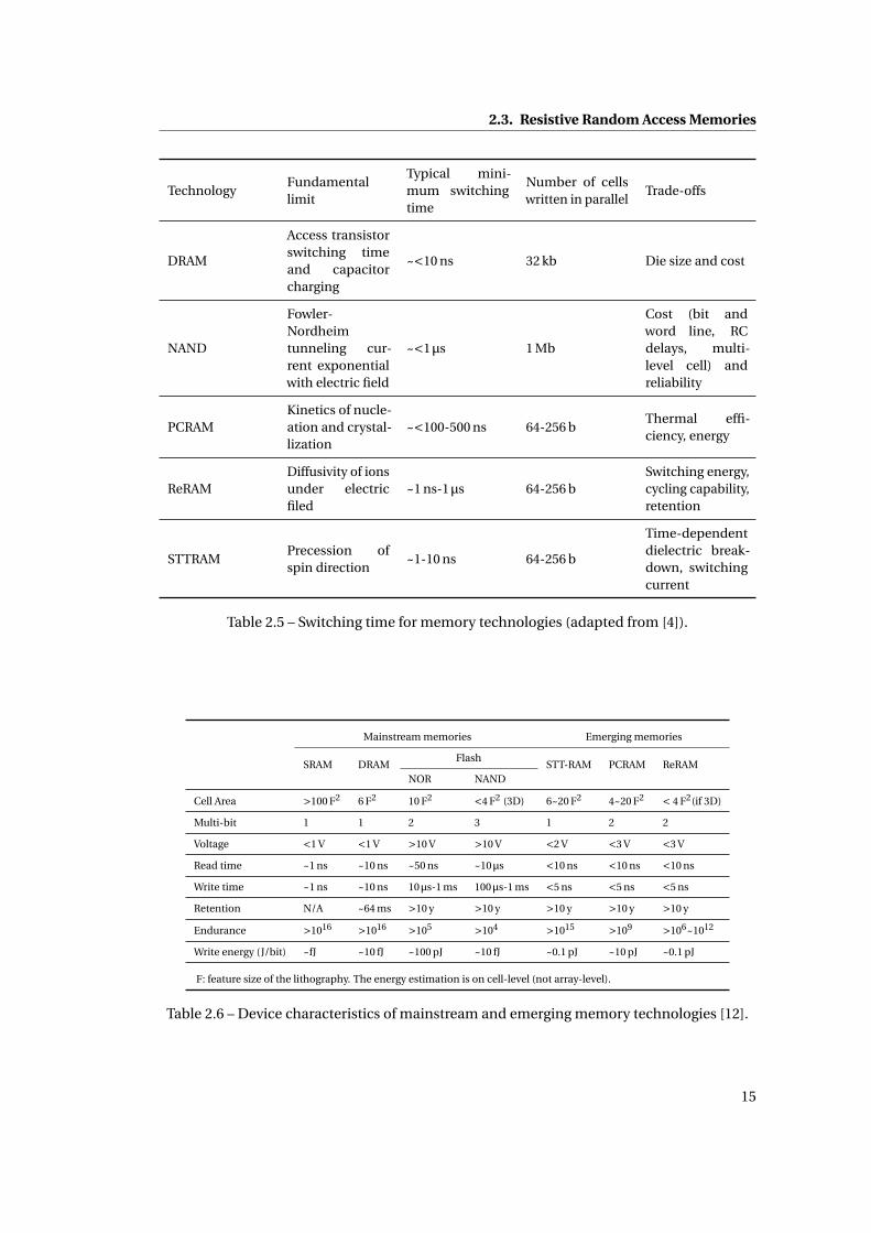
2.3. Resistive Random Access Memories
TechnologyFundamentallimit
Typical mini-mum switchingtime
Number of cellswritten in parallel
Trade-offs
DRAM
Access transistorswitching timeand capacitorcharging
~<10 ns 32 kb Die size and cost
NAND
Fowler-Nordheimtunneling cur-rent exponentialwith electric field
~<1μs 1 Mb
Cost (bit andword line, RCdelays, multi-level cell) andreliability
PCRAMKinetics of nucle-ation and crystal-lization
~<100-500 ns 64-256 bThermal effi-ciency, energy
ReRAMDiffusivity of ionsunder electricfiled
~1 ns-1μs 64-256 bSwitching energy,cycling capability,retention
STTRAMPrecession ofspin direction
~1-10 ns 64-256 b
Time-dependentdielectric break-down, switchingcurrent
Table 2.5 – Switching time for memory technologies (adapted from [4]).
Mainstream memories Emerging memories
SRAM DRAMFlash
STT-RAM PCRAM ReRAMNOR NAND
Cell Area >100 F2 6 F2 10 F2 <4 F2 (3D) 6~20 F2 4~20 F2 < 4 F2(if 3D)
Multi-bit 1 1 2 3 1 2 2
Voltage <1 V <1 V >10 V >10 V <2 V <3 V <3 V
Read time ~1 ns ~10 ns ~50 ns ~10μs <10 ns <10 ns <10 ns
Write time ~1 ns ~10 ns 10μs-1 ms 100μs-1 ms <5 ns <5 ns <5 ns
Retention N/A ~64 ms >10 y >10 y >10 y >10 y >10 y
Endurance >1016 >1016 >105 >104 >1015 >109 >106~1012
Write energy (J/bit) ~fJ ~10 fJ ~100 pJ ~10 fJ ~0.1 pJ ~10 pJ ~0.1 pJ
F: feature size of the lithography. The energy estimation is on cell-level (not array-level).
Table 2.6 – Device characteristics of mainstream and emerging memory technologies [12].
15
Chapter 2. ReRAM introduction
SrTiO3 [16]. The research activity on ReRAMs increased dramatically after Samsung demon-
strated in 2004 an array of NiO ReRAM cells integrated in 180 nm CMOS technology [17]. From
that moment, the research activity on resistive switching focused on binary transition metal
oxides such as NiO [18], TiOx [19], CuOx [20], ZrOx [21], ZnOx [22], HfOx [23], TaOx [24], AlOx
[25]. In 2008, HP labs made the connection between ReRAM and the mathematical concept
of memristor [26], which was introduced in the 70s by Chua [27]. Since 2010s, the research
on ReRAMs continued rising. An updated list of the main publications on ReRAMs (and the
other emerging non volatile memories) from 2001 up to date can be found on the webpage of
Wong’s research group in Stanford [28].
As anticipated before, in ReRAMs the memory state relies on the formation or rupture of
conductive filaments in an insulator layer. Based on the nature of the filament, ReRAMs are
classically divided into two categories: Oxide-Based ReRAM (OxRAMs) and programmable
metallization cell (or conductive-bridging RAM, CBRAM®, a registered trademark from Adesto
technologies). In OxRAMs, the oxygen vacancies in the oxide layer form conductive filaments,
which can be controlled by applying an electrical stimulus. In CBRAM, the conductive fila-
ments are created by the fast diffusion of metal ions (such as Ag or Cu) from the top electrode
into the insulating layer. In the literature, OxRAMs have been extensively reviewed by Yu [29],
while a comprehensive conductive-bridging RAM review can be found in [30].
Moreover, ReRAMs can be categorized as unipolar or bipolar according to their switching
characteristics. If the resistance state transition occurs all at one voltage polarity, the cell is
classified as unipolar. Usually unipolar cells have a symmetric structure, and the switching
mechanisms are prevalently thermally driven phenomena. On the contrary, if the resistance
state transitions require both a positive and a negative voltage polarity, the cell is referred
as bipolar. In term of performances, unipolar cells require usually larger currents and show
higher variability.
In this work we focus exclusively on bipolar oxide-based ReRAMs. For simplicity, in the
remainder of the document, the term ReRAM will be used as a synonym of bipolar OxRAM.
The ReRAM basic structure is quite simple as it consists of a stack of three or more material
layers, as it is represented in Fig. 2.3 (a). The Bottom Electrode (BE) is usually made of metals
or conductive nitrites such as TiN, TaN, Pt or W. The oxide film can consist of a large variety of
materials. The main oxides used for the resistive memories are the one described previously
(TaOx, HfOx, TiOx, AlOx...). Usually, on top of the metal oxide, it is possible to include a metallic
layer that has the function of improving the memory performances by increasing the number
of oxygen vacancies in the oxide film. This film can be constituted for example by Ta, Hf, Ti or
Zr. Finally, the Top Electrode (TE) layer is made of metallic or conductive nitride films, similarly
to the BE ones.
A schematization of the ReRAM electrical characteristics is reported in Fig. 2.3 (b). The I-V
plot shows that the memory can operate in two distinct resistance states. The red curve shows
the High Resistance State (HRS), while the blue one shows the Low Resistance State (LRS). The
16
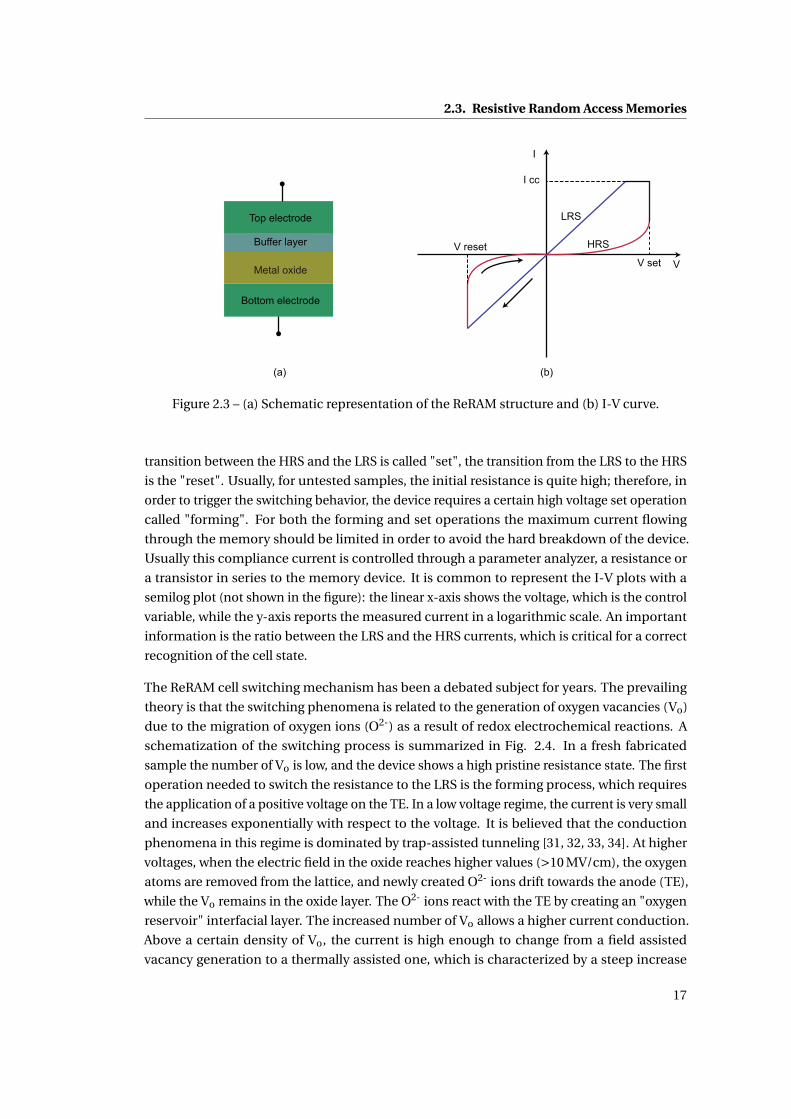
2.3. Resistive Random Access Memories
Figure 2.3 – (a) Schematic representation of the ReRAM structure and (b) I-V curve.
transition between the HRS and the LRS is called "set", the transition from the LRS to the HRS
is the "reset". Usually, for untested samples, the initial resistance is quite high; therefore, in
order to trigger the switching behavior, the device requires a certain high voltage set operation
called "forming". For both the forming and set operations the maximum current flowing
through the memory should be limited in order to avoid the hard breakdown of the device.
Usually this compliance current is controlled through a parameter analyzer, a resistance or
a transistor in series to the memory device. It is common to represent the I-V plots with a
semilog plot (not shown in the figure): the linear x-axis shows the voltage, which is the control
variable, while the y-axis reports the measured current in a logarithmic scale. An important
information is the ratio between the LRS and the HRS currents, which is critical for a correct
recognition of the cell state.
The ReRAM cell switching mechanism has been a debated subject for years. The prevailing
theory is that the switching phenomena is related to the generation of oxygen vacancies (Vo)
due to the migration of oxygen ions (O2-) as a result of redox electrochemical reactions. A
schematization of the switching process is summarized in Fig. 2.4. In a fresh fabricated
sample the number of Vo is low, and the device shows a high pristine resistance state. The first
operation needed to switch the resistance to the LRS is the forming process, which requires
the application of a positive voltage on the TE. In a low voltage regime, the current is very small
and increases exponentially with respect to the voltage. It is believed that the conduction
phenomena in this regime is dominated by trap-assisted tunneling [31, 32, 33, 34]. At higher
voltages, when the electric field in the oxide reaches higher values (>10 MV/cm), the oxygen
atoms are removed from the lattice, and newly created O2- ions drift towards the anode (TE),
while the Vo remains in the oxide layer. The O2- ions react with the TE by creating an "oxygen
reservoir" interfacial layer. The increased number of Vo allows a higher current conduction.
Above a certain density of Vo, the current is high enough to change from a field assisted
vacancy generation to a thermally assisted one, which is characterized by a steep increase
17
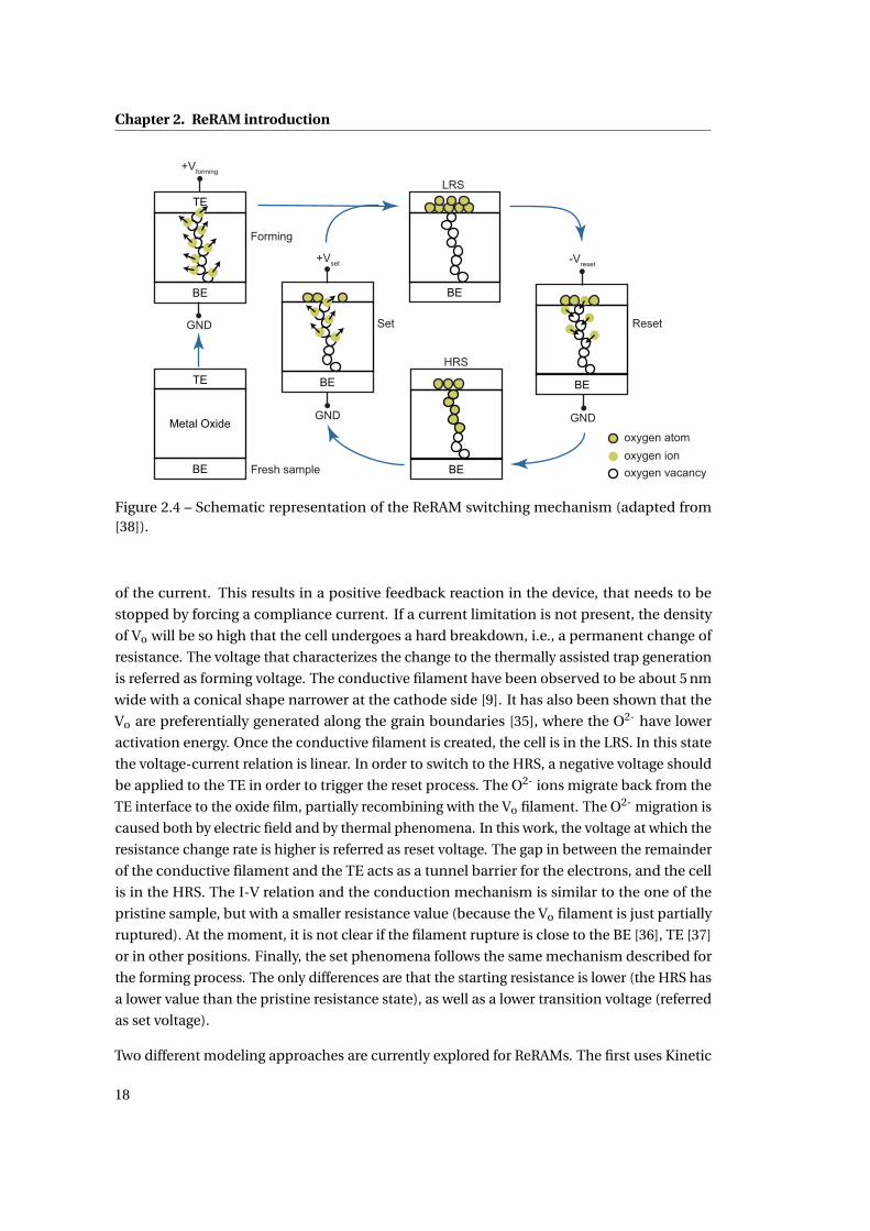
Chapter 2. ReRAM introduction
Figure 2.4 – Schematic representation of the ReRAM switching mechanism (adapted from[38]).
of the current. This results in a positive feedback reaction in the device, that needs to be
stopped by forcing a compliance current. If a current limitation is not present, the density
of Vo will be so high that the cell undergoes a hard breakdown, i.e., a permanent change of
resistance. The voltage that characterizes the change to the thermally assisted trap generation
is referred as forming voltage. The conductive filament have been observed to be about 5 nm
wide with a conical shape narrower at the cathode side [9]. It has also been shown that the
Vo are preferentially generated along the grain boundaries [35], where the O2- have lower
activation energy. Once the conductive filament is created, the cell is in the LRS. In this state
the voltage-current relation is linear. In order to switch to the HRS, a negative voltage should
be applied to the TE in order to trigger the reset process. The O2- ions migrate back from the
TE interface to the oxide film, partially recombining with the Vo filament. The O2- migration is
caused both by electric field and by thermal phenomena. In this work, the voltage at which the
resistance change rate is higher is referred as reset voltage. The gap in between the remainder
of the conductive filament and the TE acts as a tunnel barrier for the electrons, and the cell
is in the HRS. The I-V relation and the conduction mechanism is similar to the one of the
pristine sample, but with a smaller resistance value (because the Vo filament is just partially
ruptured). At the moment, it is not clear if the filament rupture is close to the BE [36], TE [37]
or in other positions. Finally, the set phenomena follows the same mechanism described for
the forming process. The only differences are that the starting resistance is lower (the HRS has
a lower value than the pristine resistance state), as well as a lower transition voltage (referred
as set voltage).
Two different modeling approaches are currently explored for ReRAMs. The first uses Kinetic
18

2.3. Resistive Random Access Memories
Monte-Carlo methods to model the atomistic processes involved in the ReRAM switching
dynamic. This method is particularly indicated to study intrinsically stochastic mechanisms,
such as the ReRAM switching. Usually the simulator first calculate a 3D electric field map
from a given starting configuration of Vo and O2-. This is used to calculate the electric current
and the generated heat. The total energy is then used to update the diffusion, generation
and recombination rates of the O ions and vacancies. If this results in a change of the atom
configuration, the simulation loops back to the calculation of the electric field, and repeats
the procedure. It has been calculated that, during switching, the cell temperature rises locally
in the filament region up to 200° C [36].
The second approach for describing the ReRAM behavior is based on compact models. These
models are based on physic simplifications that allow their use in circuit design softwares.
This is required in order to enable the design of the peripheral circuit used for driving the
memory cells. Examples of models are reported in [39, 40, 41, 42]. In general, compact models
are based on relations such as the one reported in Equation 2.1:
I = I0e
(− g
g0
)sinh
(V
V0
)(2.1)
where the current I is proportional to the exponential of the gap g between the TE and the
filament. The relation between I and V is generally expressed by a hyperbolic sine function,
which allows to express a linear dependence for small values of V, and an exponential one for
high values of V. I0, g0 and V0 are fitting parameters. This equation is usually coupled with
an expression that describes the evolution of g in time, which depends exponentially on the
applied voltage, vacancy generation and the recombination energies, oxide thickness and
atomic hopping distance.
19

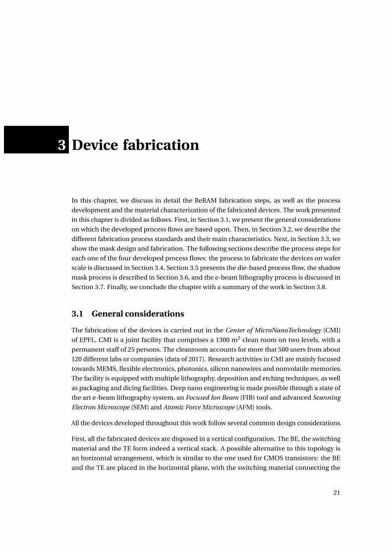
3 Device fabrication
In this chapter, we discuss in detail the ReRAM fabrication steps, as well as the process
development and the material characterization of the fabricated devices. The work presented
in this chapter is divided as follows. First, in Section 3.1, we present the general considerations
on which the developed process flows are based upon. Then, in Section 3.2, we describe the
different fabrication process standards and their main characteristics. Next, in Section 3.3, we
show the mask design and fabrication. The following sections describe the process steps for
each one of the four developed process flows: the process to fabricate the devices on wafer
scale is discussed in Section 3.4, Section 3.5 presents the die-based process flow, the shadow
mask process is described in Section 3.6, and the e-beam lithography process is discussed in
Section 3.7. Finally, we conclude the chapter with a summary of the work in Section 3.8.
3.1 General considerations
The fabrication of the devices is carried out in the Center of MicroNanoTechnology (CMI)
of EPFL. CMI is a joint facility that comprises a 1300 m2 clean room on two levels, with a
permanent staff of 25 persons. The cleanroom accounts for more that 500 users from about
120 different labs or companies (data of 2017). Research activities in CMI are mainly focused
towards MEMS, flexible electronics, photonics, silicon nanowires and nonvolatile memories.
The facility is equipped with multiple lithography, deposition and etching techniques, as well
as packaging and dicing facilities. Deep nano engineering is made possible through a state of
the art e-beam lithography system, an Focused Ion Beam (FIB) tool and advanced Scanning
Electron Microscope (SEM) and Atomic Force Microscope (AFM) tools.
All the devices developed throughout this work follow several common design considerations.
First, all the fabricated devices are disposed in a vertical configuration. The BE, the switching
material and the TE form indeed a vertical stack. A possible alternative to this topology is
an horizontal arrangement, which is similar to the one used for CMOS transistors: the BE
and the TE are placed in the horizontal plane, with the switching material connecting the
21

Chapter 3. Device fabrication
two. For ReRAMs, the horizontal configuration, if compared to the vertical one, has several
disadvantages. The current paths are are generally not straight, because the electrodes usually
sit on top of the resistive material. If not, that is the electrodes and the resistive material are
adjacent on an horizontal plane, the process is extremely complex and the interface between
the electrode and the resistive material is not controllable. Furthermore, the devices have
a lower scalability because of the loss in resolution caused by proximity effects during the
electrode lithography. Finally, for horizontal devices, the ReRAM requires a final passivation
step after the deposition of the resistive layer.
A second important point accumunating the four processes is that the resistive material is
not exposed to air. All the devices are passivated, as it is demosntrated that the switching
phenomena is sensitive to the environment [43], therefore the switching layer must be isolated
from it. As it will be discussed in Chapter 4, the type of the passivation material can also
influence the switching properties.
As a third consideration, the switching material is covered right away with the buffer layer, and
the TE is deposited immediately on top of it, without breaking the vacuum. This is needed
in order to avoid any oxidation or contamination that the films could undergo if exposed to
air. For the same reason, we do not perform any lithography process directly on top of the
switching or buffer layer. The exposure to the photoresist or solvents could indeed modify
the material properties, therefore introducing an uncontrollable variability in the fabrication
process. Furthermore, no high temperature process steps are performed after the switching
material is deposited, if not on purpose, not to induce changes in the switching material
structure.
Regarding the device topology, two type of vertical ReRAM devices are generally used: VIA and
crosspoint structures. In VIA-based devices, the passivation is deposited after the BE, and it is
patterned in order to obtain an opening (VIA) that will define the device area. On the contrary,
for crosspoint devices the device area is defined by the crossing of the TE and the BE, and not
by the passivation opening. From our experimental data, we noticed almost no difference
in performance between these two device geometries for μm-large devices. Nevertheless, in
this work, for all the optical lithography processes we focused on VIA-based devices because
it makes possible to use a self-aligned shadow mask to pattern the TE, and because it allows
more flexibility in the choice of the passivation material (there are fewer temperature budget
limitations as the passivation is deposited before the oxide material). Furthermore, in case of
devices with different active areas, the VIA-based structures ensure to have the same electrode
series resistance, which will not be the case for a crosspoint structure. Finally, for VIA devices,
the resistive material is in contact with the center of the BE, allowing a better control of the
interface and no risks for edge or sidewall effects. In crosspoint structures is indeed possible
that the switching occurs on the edge or on the sidewall of the BE.
As a final consideration, we should underline that all the fabricated ReRAMs are decoupled
from each other. We did not investigate device arrays or the cross effects that connected
22
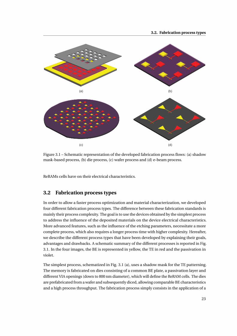
3.2. Fabrication process types
Figure 3.1 – Schematic representation of the developed fabrication process flows: (a) shadowmask-based process, (b) die process, (c) wafer process and (d) e-beam process.
ReRAMs cells have on their electrical characteristics.
3.2 Fabrication process types
In order to allow a faster process optimization and material characterization, we developed
four different fabrication process types. The difference between these fabrication standards is
mainly their process complexity. The goal is to use the devices obtained by the simplest process
to address the influence of the deposited materials on the device electrical characteristics.
More advanced features, such as the influence of the etching parameters, necessitate a more
complete process, which also requires a longer process time with higher complexity. Hereafter,
we describe the different process types that have been developed by explaining their goals,
advantages and drawbacks. A schematic summary of the different processes is reported in Fig.
3.1. In the four images, the BE is represented in yellow, the TE in red and the passivation in
violet.
The simplest process, schematized in Fig. 3.1 (a), uses a shadow mask for the TE patterning.
The memory is fabricated on dies consisting of a common BE plate, a passivation layer and
different VIA openings (down to 800 nm diameter), which will define the ReRAM cells. The dies
are prefabricated from a wafer and subsequently diced, allowing comparable BE characteristics
and a high process throughput. The fabrication process simply consists in the application of a
23

Chapter 3. Device fabrication
shadow mask used to define the top electrode and by the deposition of the memory oxide and
top electrode materials. The goal of this process is to allow a rapid prototyping of the different
ReRAM materials. The fabrication time is, once the bottom electrode die is ready, as short
as one day. The main drawback of this method is the high cell capacitance. In order to allow
a proper shadow mask alignment, the TE dimensions are considerably large (300μm). This
creates, together with the common bottom electrode plate, a cell capacitance of about 35 pF.
The presence of a large parasitic capacitor in parallel to the memory electrodes makes difficult
to limit the device current: current overshoots during fast transient are indeed proportional to
the cell parasitic capacitance.
The second process flow, shown in Fig. 3.1 (b), uses optical lithography on a die to define
the TE. The prefabricated dies consist of several BEs, which are separated for each cell, and
a VIA (down to 800 nm diameter size). The memory is created at the crossing between the
BE and the TE. The TE deposition is patterned with standard lithography and subsequently
etched. The advantage of this process is a lower cell capacitance (below pF), a reasonable
process time (about a couple of days), while the main challenges derive from the TE etch. The
etch parameters need to be adjusted taking into account the small surface of the die and the
low temperature conductance with the chuck (the die lays on a wafer, and it is attached to it
by a wax). If the etch parameters are not controlled properly, they may induce damages in
the ReRAM dielectric because of charge accumulations. This usually results in a low pristine
resistance state.
The third process type is performed on a full wafer, shown in Fig. 3.1 (c). In this case, there
are no prefabricated dies or structures, and all the process is carried at the wafer-scale. The
resulting devices are the same as the one described in the previous paragraph. The ability
to work on a full wafer allows a large number of devices and a better control of the etching
parameters, while it requires a much longer fabrication time (in the order of a couple of weeks).
The forth and last process [Fig. 3.1 (d)] is also based on a full wafer, but it employs e-beam
lithography. This allows to fabricate devices with much smaller dimensions. With this process,
we created working devices at dimensions as small as 40 nm×40 nm. The main drawback is
the time to develop such a process flow, and the large number of optimizations required each
time that the cell structure is modified (change of materials, thicknesses...). The exposure dose
and the etching recipes need to be calibrated and modified for every material selection.
During this work, we used different process flow for the different stages of the technology
development. New materials were first explored using the shadow mask process in order to
establish the basic working parameters. These are refined further using the more advanced
processes. The main results presented in this work are based on the die process, while the
wafer process is used mainly for retention analysis. The e-beam process has been principally
used to demonstrate the technology scalability.
24

3.3. Mask design and fabrication
3.3 Mask design and fabrication
The photolithography masks used for the optical lithography processes have been designed
and fabricated internally. The mask design is realized with Cadence Virtuoso, a software dedi-
cated to designing full-custom integrated circuits. In this section, we proceed by describing
just the wafer-based process masks, as the die-based process and the shadow mask one are
designed and fabricated in a very similar way.
The top view of the wafer-level layout is reported in Fig. 3.2 (a). The design is modular and
it consists of the main blocks highlighted in the figure. The characterization die is used as a
substrate for optional tests on the material structure and properties. It includes features for
the resistivity measurements of the electrode materials and areas dedicated to the sample
preparation for Transmission Electron Microscope (TEM) or X-Ray Photoemission Spectroscopy
(XPS) analysis. The alignment mark areas include alignment marks for the optical lithography,
resolution test patterns to determine the lithography resolution, alignment tests patterns to
quantify the misalignment and e-beam alignment marks. Finally the ReRAM die ares hosts
the memory devices. Due to the complexity of the layout, a semi-automatic approach has
been adopted for the ReRAM die composition. First, we designed a basic ReRAM cell with a
parametric VIA diameter. Then, a custom procedure written in SKILL programming language
allows the placement, alignment and parametrization of the ReRAM cell. More in detail, the
software automatically generates devices with different diameter dimensions, and to insert
reference numbers to indicate the VIA diameter, the device row and column number. The
SKILL code for the wafer layout is given in Appendix B. The basic block that constitutes the
ReRAM dies, obtained by the SKILL procedure, is shown in Fig. 3.2 (b). The BE and TE pads
are 100μm × 100μm, while the electrodes adjacent to the VIA measure 20μm in width. The
mask VIA diameters were set to 1.5μm, 2μm, 3μm, 5μm and 10μm. During the mask design,
we accounted for an alignment tolerance of 5μm, and for a minimum feature of 1.5μm. By
underexposing the patterns we were able to scale down the minimum feature to 800 nm, which
is about the limit for optical lithography in CMI.
Regarding the electrode dimensions, it is believed that the parasitic capacitance of the metal
lines do not significantly affect the device electrical characteristics. For our design, the passi-
vation layer thickness is typically hundred times higher than the resistive layer thickness, and
the metal line capacitance is at worst case comparable to the memory element capacitance.
The design patterns, after conversion, are transferred on 5” Cr blanks (Cr 90 nm, PR AZ1512
530 nm) using a 5 mm head on a Heidelberg VPG 200 mask laser writer. The fragmentation
parameters and laser writing head can render up to 700 nm resolution of critical features
without significant stitching errors between the design fragments. An increased Line Edge
Roughness (LER) of features with critical dimension close to the resolution limit has been
observed. It is believed that LER does not play any significant role for VIAs with a μm critical
dimension.
Following exposure, the Cr blanks are developed in diluted AZ 351B and etched in a mixture of
25
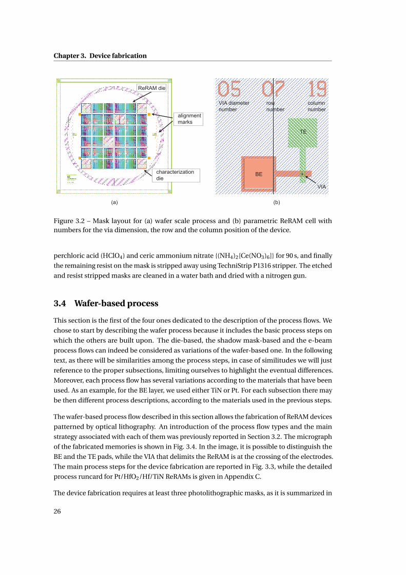
Chapter 3. Device fabrication
Figure 3.2 – Mask layout for (a) wafer scale process and (b) parametric ReRAM cell withnumbers for the via dimension, the row and the column position of the device.
perchloric acid (HClO4) and ceric ammonium nitrate {(NH4)2[Ce(NO3)6]} for 90 s, and finally
the remaining resist on the mask is stripped away using TechniStrip P1316 stripper. The etched
and resist stripped masks are cleaned in a water bath and dried with a nitrogen gun.
3.4 Wafer-based process
This section is the first of the four ones dedicated to the description of the process flows. We
chose to start by describing the wafer process because it includes the basic process steps on
which the others are built upon. The die-based, the shadow mask-based and the e-beam
process flows can indeed be considered as variations of the wafer-based one. In the following
text, as there will be similarities among the process steps, in case of similitudes we will just
reference to the proper subsections, limiting ourselves to highlight the eventual differences.
Moreover, each process flow has several variations according to the materials that have been
used. As an example, for the BE layer, we used either TiN or Pt. For each subsection there may
be then different process descriptions, according to the materials used in the previous steps.
The wafer-based process flow described in this section allows the fabrication of ReRAM devices
patterned by optical lithography. An introduction of the process flow types and the main
strategy associated with each of them was previously reported in Section 3.2. The micrograph
of the fabricated memories is shown in Fig. 3.4. In the image, it is possible to distinguish the
BE and the TE pads, while the VIA that delimits the ReRAM is at the crossing of the electrodes.
The main process steps for the device fabrication are reported in Fig. 3.3, while the detailed
process runcard for Pt/HfO2/Hf/TiN ReRAMs is given in Appendix C.
The device fabrication requires at least three photolithographic masks, as it is summarized in
26
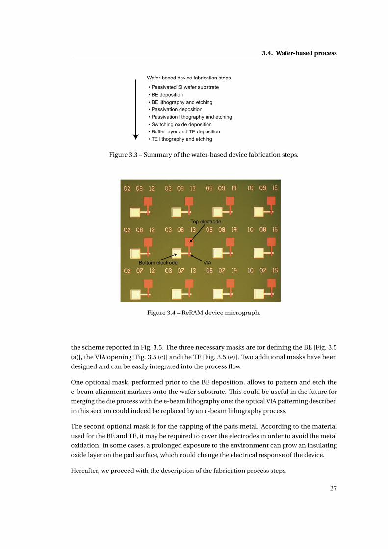
3.4. Wafer-based process
Figure 3.3 – Summary of the wafer-based device fabrication steps.
Figure 3.4 – ReRAM device micrograph.
the scheme reported in Fig. 3.5. The three necessary masks are for defining the BE [Fig. 3.5
(a)], the VIA opening [Fig. 3.5 (c)] and the TE [Fig. 3.5 (e)]. Two additional masks have been
designed and can be easily integrated into the process flow.
One optional mask, performed prior to the BE deposition, allows to pattern and etch the
e-beam alignment markers onto the wafer substrate. This could be useful in the future for
merging the die process with the e-beam lithography one: the optical VIA patterning described
in this section could indeed be replaced by an e-beam lithography process.
The second optional mask is for the capping of the pads metal. According to the material
used for the BE and TE, it may be required to cover the electrodes in order to avoid the metal
oxidation. In some cases, a prolonged exposure to the environment can grow an insulating
oxide layer on the pad surface, which could change the electrical response of the device.
Hereafter, we proceed with the description of the fabrication process steps.
27
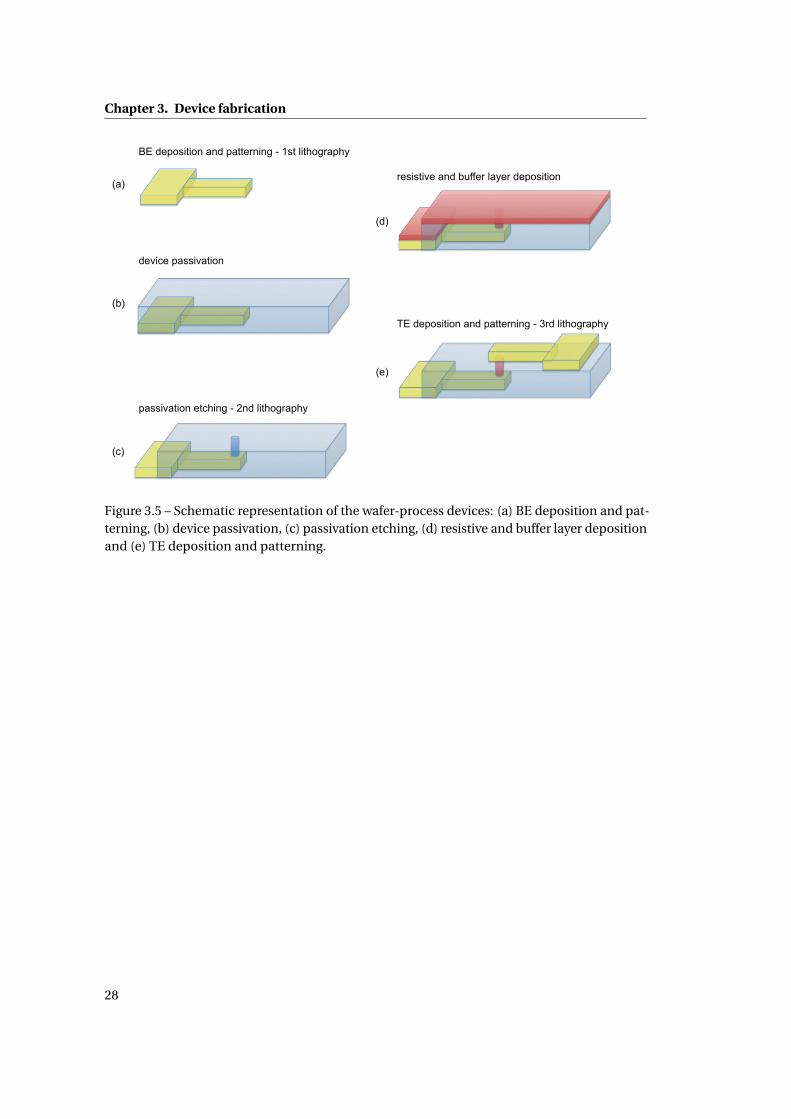
Chapter 3. Device fabrication
Figure 3.5 – Schematic representation of the wafer-process devices: (a) BE deposition and pat-terning, (b) device passivation, (c) passivation etching, (d) resistive and buffer layer depositionand (e) TE deposition and patterning.
28
3.4. Wafer-based process
3.4.1 Substrate
All memories are fabricated on 4” Si <100> test wafers. The top side of the wafer is polished,
and the substrate has a thickness of 525μm. The wafers are p-doped (B) with a resistivity in the
range of 0.1 - 100Ω·cm. Because the Si substrate is not a part of the device, a relatively large
variation in the resitivity does not affect the device characteristics. A 500 nm SiO2 film grown
by wet oxidation is pre-processed on the wafer, which main purpose is to provide electrical
insulation between the devices and the wafer substrate.
3.4.2 Bottom electrode deposition
Before the electrode metal depositions, the wafer is rinsed with deionized water in a Spin
Rinse Dryer (SRD) machine. It is then exposed to a 5 min O plasma (1000 W, 300 sccm O2) at
low vacuum (700 mTorr) in order to remove eventual traces of organic materials. The electrode
metal layer (Pt or TiN) is deposited by sputtering at room temperature in a Pfeiffer SPIDER 600
cluster system.
For Pt BE, 5 nm Ti adhesion layer is deposited by DC sputtering with a 9 sccm Ar flow as
ionizing gas in a 1000 W plasma. The Ti layer is critical in order to allow the adhesion of the
BE onto the underlying SiO2 layer. A thinner Ti film would result in poor adhesion promoting
properties, while diffusion of Ti into Pt films when exposed to high-temperature annealing
steps are reported for Ti thicknesses above 10 nm [44].
The Pt BE is deposited right after the adhesion layer without breaking the vacuum. The
electrode is deposited using DC sputtering and Ar as the ionizing gas (15 sccm) in a 1000 W
plasma. The Pt film thickness is fixed to 125 nm, with a measured deposition rate of 46 Å/s.
The calibration of the deposition rate was performed by using a high-resolution profilometer
both on dummy samples and on the ReRAM devices, measured after the BE pattering. The
deposition rate showed less than a 7% deviation of the mean thickness with respect to the
nominal values.
TiN is deposited by RF magnetron reactive sputtering from a Ti target with Ar (40 sccm) and N2
(40 sccm) gases in a 1000 W plasma. The TiN film thickness is fixed to 200 nm, with a measured
deposition rate of 2.46 Å/s calibrated by profilometer. A 9% deviation of the mean thickness
values has been measured with respect to the target deposition rate. The resistivity of the TiN
film, measured by a four-point measurement resistivity meter, was 3.5-6.4×10⁻⁸ Ω·m.
3.4.3 Bottom electrode lithography
Prior to the photoresist coating, a surface preparation step is needed to improve the adhesion
of the photoresist material to the substrate. According to the type of the BE material, different
techniques can be adopted. In case of Pt, we exposed the wafer to an O2 plasma (1000 W,
300 sccm O2, 0.7 mTorr) for 30 s. For TiN, the wafer is dehydrated at 125° C for 5 min. These
29
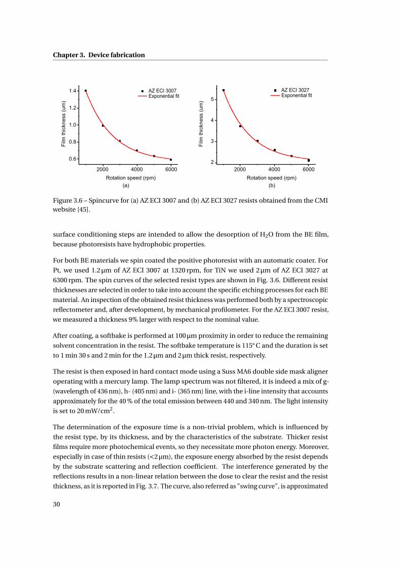
Chapter 3. Device fabrication
Figure 3.6 – Spincurve for (a) AZ ECI 3007 and (b) AZ ECI 3027 resists obtained from the CMIwebsite [45].
surface conditioning steps are intended to allow the desorption of H2O from the BE film,
because photoresists have hydrophobic properties.
For both BE materials we spin coated the positive photoresist with an automatic coater. For
Pt, we used 1.2μm of AZ ECI 3007 at 1320 rpm, for TiN we used 2μm of AZ ECI 3027 at
6300 rpm. The spin curves of the selected resist types are shown in Fig. 3.6. Different resist
thicknesses are selected in order to take into account the specific etching processes for each BE
material. An inspection of the obtained resist thickness was performed both by a spectroscopic
reflectometer and, after development, by mechanical profilometer. For the AZ ECI 3007 resist,
we measured a thickness 9% larger with respect to the nominal value.
After coating, a softbake is performed at 100μm proximity in order to reduce the remaining
solvent concentration in the resist. The softbake temperature is 115° C and the duration is set
to 1 min 30 s and 2 min for the 1.2μm and 2μm thick resist, respectively.
The resist is then exposed in hard contact mode using a Suss MA6 double side mask aligner
operating with a mercury lamp. The lamp spectrum was not filtered, it is indeed a mix of g-
(wavelength of 436 nm), h- (405 nm) and i- (365 nm) line, with the i-line intensity that accounts
approximately for the 40 % of the total emission between 440 and 340 nm. The light intensity
is set to 20 mW/cm2.
The determination of the exposure time is a non-trivial problem, which is influenced by
the resist type, by its thickness, and by the characteristics of the substrate. Thicker resist
films require more photochemical events, so they necessitate more photon energy. Moreover,
especially in case of thin resists (<2μm), the exposure energy absorbed by the resist depends
by the substrate scattering and reflection coefficient. The interference generated by the
reflections results in a non-linear relation between the dose to clear the resist and the resist
thickness, as it is reported in Fig. 3.7. The curve, also referred as "swing curve", is approximated
30
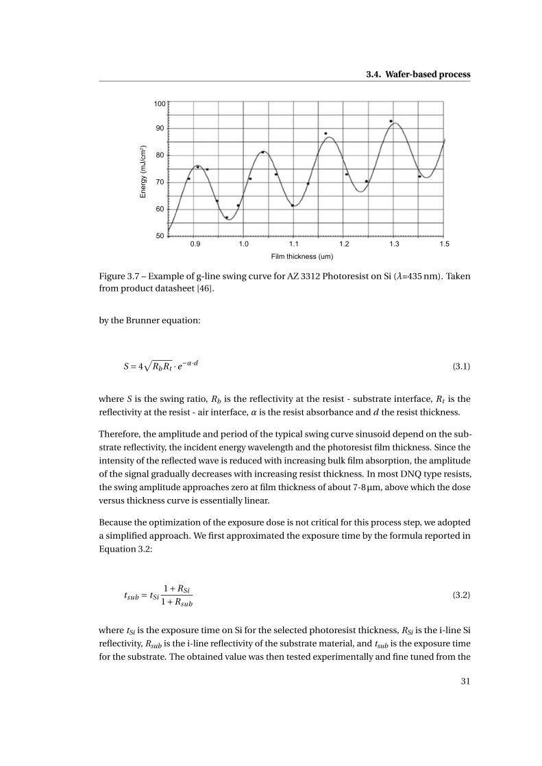
3.4. Wafer-based process
Figure 3.7 – Example of g-line swing curve for AZ 3312 Photoresist on Si (λ=435 nm). Takenfrom product datasheet [46].
by the Brunner equation:
S = 4√
RbRt ·e−α·d (3.1)
where S is the swing ratio, Rb is the reflectivity at the resist - substrate interface, Rt is the
reflectivity at the resist - air interface, α is the resist absorbance and d the resist thickness.
Therefore, the amplitude and period of the typical swing curve sinusoid depend on the sub-
strate reflectivity, the incident energy wavelength and the photoresist film thickness. Since the
intensity of the reflected wave is reduced with increasing bulk film absorption, the amplitude
of the signal gradually decreases with increasing resist thickness. In most DNQ type resists,
the swing amplitude approaches zero at film thickness of about 7-8μm, above which the dose
versus thickness curve is essentially linear.
Because the optimization of the exposure dose is not critical for this process step, we adopted
a simplified approach. We first approximated the exposure time by the formula reported in
Equation 3.2:
tsub = tSi1+RSi
1+Rsub(3.2)
where tSi is the exposure time on Si for the selected photoresist thickness, RSi is the i-line Si
reflectivity, Rsub is the i-line reflectivity of the substrate material, and tsub is the exposure time
for the substrate. The obtained value was then tested experimentally and fine tuned from the
31
Chapter 3. Device fabrication
result of the exposure test structures transferred on the wafer. The exposure times used for the
lithography are 9 s for the lithography on TiN (2μm resist), and 6.5 s for the lithography on Pt
(1.2μm resist). These exposure time are maximum 8% different from the ones obtained from
the simplified model reported in Equation 3.2.
After exposure, the resist is developed in an automatic developer line with an initial spray
dispense followed by puddle method using AZ 726 MIF developer. An hardbake with a large
gap between the wafer and the heater is finally applied in order to improve the resist thermal
stability.
The highest resolution achievable for this lithography line was about 800 nm (which was
obtained for the VIA lithography, while the BE lithography resolution was around 1.2μm).
This limit comes from the spectrum of exposure light (which is a broadband spectrum, as it
is not just composed of the i-line spectrum), from the mask resolution, from the thickness
of the photoresist film, from the type of exposure and from the high reflectivity of the metal
substrates. The BE lithography step was not optimized excessively because the minimum
features were quite large, and because the BE resolution does not have a real impact on
VIA-based devices. Possible improvements would have been the use of a thinner photoresist
film (and, by consequence, a thinner BE metal) or the implementation of bottom and top
antireflective coatings.
3.4.4 Bottom electrode etching
The BE metal is etched by a Reactive Ion Etching (RIE) process in a STS Multiplex ICP dry
etcher. First, the chamber is cleaned with a 5 min O-based plasma (50 sccm O2, 20 mTorr) at
800 W performed on a dummy wafer passivated with SiO2. This operation allows cleaning
the chamber from organic residues. Next, a chamber pre-conditioning step is run on a SiO2
passivated dummy wafer for 5 min. This second etching is based on an O2 (16 sccm) and
SF6 (100 sccm) plasma at 800 W and 30 mTorr. The aim of this process is the redeposition of
fluorite compounds, generated from the etching of the SiO2 film, on the chamber sidewalls.
This allows having a controlled chamber condition prior to the BE etching. The two indicators
that can be used in order to determine the status of the cleaning and conditioning steps
are the plasma color and the APC angle. The plasma color should be violet-pink during the
conditioning step, white for the Pt etching and white for the TiN etch. A second indicator is
the automatic pressure controller valve, or APC, which controls the pressure in the reactor.
For clean chamber conditions, the APC angle should drop below 65°during the cleaning step.
In case of Pt, the etching plasma is composed of Ar (70 sccm) and Cl2 (20 sccm) at 3 mTorr,
with a power of 800 W and 150 W applied on the coil and on the platen, respectively. The Pt
etching recipe is quite isotropic and physical. The process is stopped by a laser end point
detection. The intensity of the laser beam reflected by the substrate is monitored, and, as the
highly reflective BE is etched, the laser signal drops. The etching time is typically 3 min 05 s,
taking into account the overetching. This time increases of about 10 s for each consecutive
32
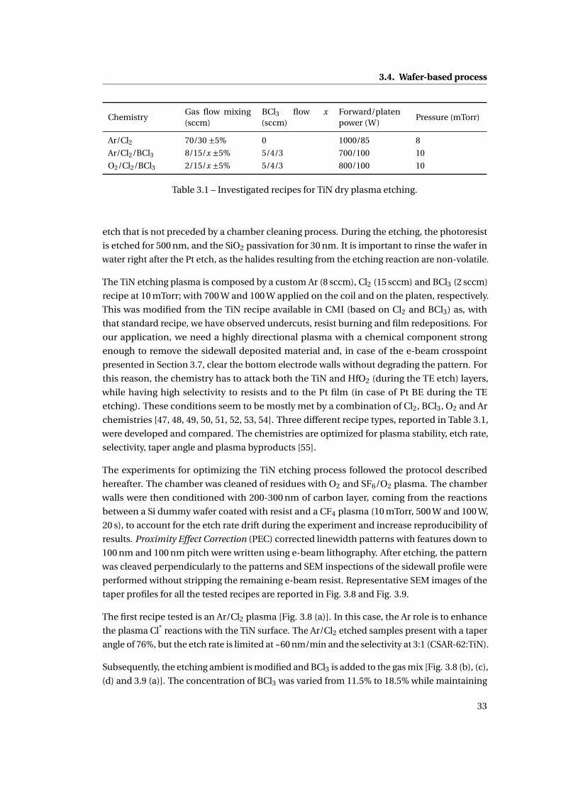
3.4. Wafer-based process
ChemistryGas flow mixing(sccm)
BCl3 flow x(sccm)
Forward/platenpower (W)
Pressure (mTorr)
Ar/Cl2 70/30 ±5% 0 1000/85 8
Ar/Cl2/BCl3 8/15/x ±5% 5/4/3 700/100 10
O2/Cl2/BCl3 2/15/x ±5% 5/4/3 800/100 10
Table 3.1 – Investigated recipes for TiN dry plasma etching.
etch that is not preceded by a chamber cleaning process. During the etching, the photoresist
is etched for 500 nm, and the SiO2 passivation for 30 nm. It is important to rinse the wafer in
water right after the Pt etch, as the halides resulting from the etching reaction are non-volatile.
The TiN etching plasma is composed by a custom Ar (8 sccm), Cl2 (15 sccm) and BCl3 (2 sccm)
recipe at 10 mTorr; with 700 W and 100 W applied on the coil and on the platen, respectively.
This was modified from the TiN recipe available in CMI (based on Cl2 and BCl3) as, with
that standard recipe, we have observed undercuts, resist burning and film redepositions. For
our application, we need a highly directional plasma with a chemical component strong
enough to remove the sidewall deposited material and, in case of the e-beam crosspoint
presented in Section 3.7, clear the bottom electrode walls without degrading the pattern. For
this reason, the chemistry has to attack both the TiN and HfO2 (during the TE etch) layers,
while having high selectivity to resists and to the Pt film (in case of Pt BE during the TE
etching). These conditions seem to be mostly met by a combination of Cl2, BCl3, O2 and Ar
chemistries [47, 48, 49, 50, 51, 52, 53, 54]. Three different recipe types, reported in Table 3.1,
were developed and compared. The chemistries are optimized for plasma stability, etch rate,
selectivity, taper angle and plasma byproducts [55].
The experiments for optimizing the TiN etching process followed the protocol described
hereafter. The chamber was cleaned of residues with O2 and SF6/O2 plasma. The chamber
walls were then conditioned with 200-300 nm of carbon layer, coming from the reactions
between a Si dummy wafer coated with resist and a CF4 plasma (10 mTorr, 500 W and 100 W,
20 s), to account for the etch rate drift during the experiment and increase reproducibility of
results. Proximity Effect Correction (PEC) corrected linewidth patterns with features down to
100 nm and 100 nm pitch were written using e-beam lithography. After etching, the pattern
was cleaved perpendicularly to the patterns and SEM inspections of the sidewall profile were
performed without stripping the remaining e-beam resist. Representative SEM images of the
taper profiles for all the tested recipes are reported in Fig. 3.8 and Fig. 3.9.
The first recipe tested is an Ar/Cl2 plasma [Fig. 3.8 (a)]. In this case, the Ar role is to enhance
the plasma Cl* reactions with the TiN surface. The Ar/Cl2 etched samples present with a taper
angle of 76%, but the etch rate is limited at ~60 nm/min and the selectivity at 3:1 (CSAR-62:TiN).
Subsequently, the etching ambient is modified and BCl3 is added to the gas mix [Fig. 3.8 (b), (c),
(d) and 3.9 (a)]. The concentration of BCl3 was varied from 11.5% to 18.5% while maintaining
33
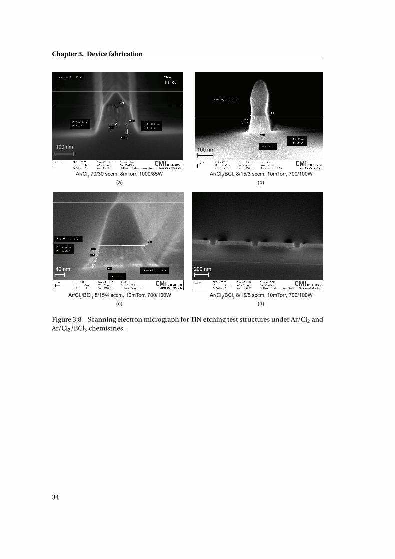
Chapter 3. Device fabrication
Figure 3.8 – Scanning electron micrograph for TiN etching test structures under Ar/Cl2 andAr/Cl2/BCl3 chemistries.
34
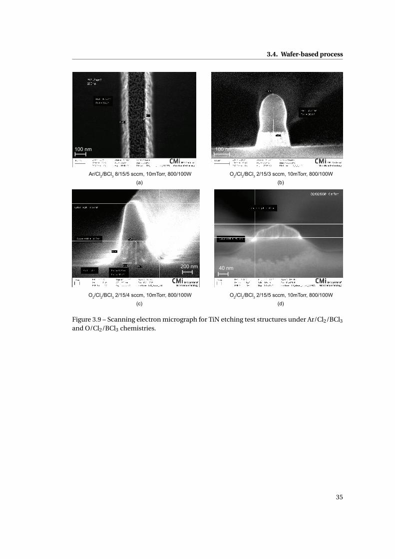
3.4. Wafer-based process
Figure 3.9 – Scanning electron micrograph for TiN etching test structures under Ar/Cl2/BCl3
and O/Cl2/BCl3 chemistries.
35
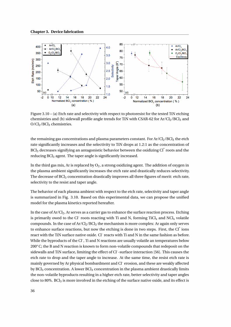
Chapter 3. Device fabrication
Figure 3.10 – (a) Etch rate and selectivity with respect to photoresist for the tested TiN etchingchemistries and (b) sidewall profile angle trends for TiN with CSAR-62 for Ar/Cl2/BCl3 andO/Cl2/BCl3 chemistries.
the remaining gas concentrations and plasma parameters constant. For Ar/Cl2/BCl3 the etch
rate significantly increases and the selectivity to TiN drops at 1.2:1 as the concentration of
BCl3 decreases signifying an antagonistic behavior between the oxidizing Cl* roots and the
reducing BCl3 agent. The taper angle is significantly increased.
In the third gas mix, Ar is replaced by O2, a strong oxidizing agent. The addition of oxygen in
the plasma ambient significantly increases the etch rate and drastically reduces selectivity.
The decrease of BCl3 concentration drastically improves all three figures of merit: etch rate,
selectivity to the resist and taper angle.
The behavior of each plasma ambient with respect to the etch rate, selectivity and taper angle
is summarized in Fig. 3.10. Based on this experimental data, we can propose the unified
model for the plasma kinetics reported hereafter.
In the case of Ar/Cl2, Ar serves as a carrier gas to enhance the surface reaction process. Etching
is primarily owed to the Cl- roots reacting with Ti and N, forming TiClx and NClx volatile
compounds. In the case of Ar/Cl2/BCl3 the mechanism is more complex: Ar again only serves
to enhance surface reactions, but now the etching is done in two steps. First, the Cl* ions
react with the TiN surface native oxide. Cl- reacts with Ti and N in the same fashion as before.
While the byproducts of the Cl-, Ti and N reactions are usually volatile an temperatures below
200° C; the B and N reaction is known to form non-volatile compounds that redeposit on the
sidewalls and TiN surface, limiting the effect of Cl--surface interaction [56]. This causes the
etch rate to drop and the taper angle to increase. At the same time, the resist etch rate is
mainly governed by Ar physical bombardment and Cl- erosion, and these are weakly affected
by BCl3 concentration. A lower BCl3 concentration in the plasma ambient drastically limits
the non-volatile byproducts resulting in a higher etch rate, better selectivity and taper angles
close to 80%. BCl3 is more involved in the etching of the surface native oxide, and its effect is
36
3.4. Wafer-based process
critical only in the first stage of the etching process. On the contrary, the bulk of the material is
etched by the Ar activated Cl2. Replacing Ar with O2 creates an additional reaction forming
TiOx and NOx volatile compounds, resulting in boosting of the etch rate. The mask erosion
also increases but at a slower rate hence the optimal selectivity values. All recipes are limited
to a maximum angle signifying that either BCl3 has to further decrease or Cl2 concentration
increase.
The TiN BE etching process, as for Pt, is stopped by laser end point detection. The etching time
is typically 3 min, taking into account some overetching. For TiN, the process time increases
about 5 s for each consecutive etch, and the photoresist etching rate increases as well. The
photoresist is etched for 650 nm, and the SiO2 passivation for 100 nm, with a roughness of
about 20 nm. For both Pt and TiN RIEs, the etching rate is faster on the outside part of the
wafer than on the center. This phenomena, a well-known uniformity problem for dry etchings,
is also referred as "bull’s eye" effect. This derive from the relative selectivity of the wafer
surface with respect to the cathode material, and it is deteriorated further from the use of
barrel reactors (as the STS Multiplex ICP dry etcher). In this case, circular interference patterns
result due to the lower or higher consumption of the reactants between the regions above the
wafer and cathode material.
After the etching process, the wafer is right away rinsed in water.
3.4.5 Resist strip
For both RIE recipes, the resist undergoes some hardening due to the prolonged exposure to
the plasma. In case of Pt bottom electrode, the procedure to strip the resist is the following.
First, the wafer is exposed to a 3 min O plasma (1000 W, 300 sccm O2) at low vacuum (700 mTorr)
in order to crack the resist hard skin. The photoresist etching rate is 35 nm/min, so the bulk
of the resist is still present after this plasma step. The photoresist removal is complete with
a 15 min wet etching in a MICROPOSIT® Remover 1165 solution at 70° C. The wafer is then
rinsed and dried.
In case of TiN, it is not possible to proceed with the O plasma etching, because this would
heavily oxidize the BE. Moreover, a photoresist strip uniquely based on wet etching was not a
sufficiently reliable method. Occasionally, the bulk of the resist is dissolved by the remover
solution, but the resist hard skin falls onto the BE surface contaminating it irreversibly. The
most reliable process to remove the resist was a H-based RIE. The plasma is created in a
SPTS APS dielectric etcher with 50 sccm of H2 at 50 mTorr, and with a power of 1000 W and
30 W on the coil and on the platen, respectively. The He pressure for the backside cooling
has been limited on purpose to 5 Torr in order to increase the temperature of the wafer, and,
consequently, the etching rate. The photoresist etch rate is 70 nm/min, and the total process
time 18 min 30 s. The wafer is finally rinsed and dried.
A SEM image of a TiN BE after the etching and the photoresist strip with a H plasma is shown
37
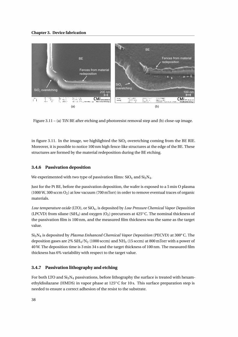
Chapter 3. Device fabrication
Figure 3.11 – (a) TiN BE after etching and photoresist removal step and (b) close-up image.
in figure 3.11. In the image, we highlighted the SiO2 overetching coming from the BE RIE.
Moreover, it is possible to notice 100 nm high fence-like structures at the edge of the BE. These
structures are formed by the material redeposition during the BE etching.
3.4.6 Passivation deposition
We experimented with two type of passivation films: SiOx and Si3N4.
Just for the Pt BE, before the passivation deposition, the wafer is exposed to a 5 min O plasma
(1000 W, 300 sccm O2) at low vacuum (700 mTorr) in order to remove eventual traces of organic
materials.
Low temperature oxide (LTO), or SiOx, is deposited by Low Pressure Chemical Vapor Deposition
(LPCVD) from silane (SiH4) and oxygen (O2) precursors at 425° C. The nominal thickness of
the passivation film is 100 nm, and the measured film thickness was the same as the target
value.
Si3N4 is deposited by Plasma Enhanced Chemical Vapor Deposition (PECVD) at 300° C. The
deposition gases are 2% SiH4/N2 (1000 sccm) and NH3 (15 sccm) at 800 mTorr with a power of
40 W. The deposition time is 3 min 34 s and the target thickness of 100 nm. The measured film
thickness has 6% variability with respect to the target value.
3.4.7 Passivation lithography and etching
For both LTO and Si3N4 passivations, before lithography the surface is treated with hexam-
ethyldisilazane (HMDS) in vapor phase at 125° C for 10 s. This surface preparation step is
needed to ensure a correct adhesion of the resist to the substrate.
38
3.4. Wafer-based process
An AZ ECI 3007 resist of nominal thickness of 600 nm is coated on the wafer at 6700 rpm,
followed by a 1 min softbake at 115° C. The exposure is performed with the same modality
described for the BE in the Subsection 3.4.3, with an exposure time of 4.8 s. The wafer is on
purpose underexposed in order to obtain feature smaller than the mask resolution. As for the
BE lithography, after exposure the resist is developed in AZ 726 MIF developer. A hardbake
is finally applied to the wafer in order to improve the resist thermal stability. The measured
photoresist thickness, after the development step, is 520 nm. The alignment error with respect
to the previous mask is below 3μm.
The LTO substrates are then exposed to a 30 s O plasma etching (200 sccm O2, 0.5 mbar, 200 W)
in order to remove the non developed photoresist residuals. The passivation is then etched
by wet etching using a Buffered Hydrofluoric Acid (BHF) solution composed of seven parts of
40% NH4F in water and one part of 49% HF in water. A 22 s etching is sufficient to completely
remove the LTO layer, while, because of the different etching rate, there is almost no etching of
the underlying SiO2 layer grown by wet oxidation.
In case of the Si3N4 passivation film, the etching process is a RIE in a SPTS APS dielectric
etcher. The plasma is created from CHF3 (50 sccm) and SF6 (10 sccm) gases at 15 mTorr
applying 950 W and 20 W on the coil and platen, respectively. The Si3N4 is etched after 35 s,
with a 42 nm overetch of the underlying SiO2 layer grown by wet oxidation, and 80 nm etching
of the photoresist.
The photoresist is then stripped similarly to what has been described in Subsection 3.4.5. For
Pt BE devices, the strip method consists of a O plasma etching followed by a wet etching, while
for TiN BE devices, the photoresist strip consist of a 8 min 30 s H plasma.
A SEM image of a VIA after the wet etching and the photoresist strip is reported in Fig. 3.12.
Fig. 3.12 (a) shows a 10μm diameter VIA wet etched in a SiO2 passivation of a Pt BE device.
The close-up image of a 3μm diameter VIA sidewall for a TiN BE device is shown in Fig. 3.12
(b).
3.4.8 Switching oxide deposition
Before the deposition of the switching oxide layer, we cleaned the surface of the BE. For Pt BEs,
the wafer is exposed to a 1 min O plasma (1000 W, 300 sccm O2) at low vacuum (700 mTorr).
For TiN BEs, we introduced a wet etching cleaning step to remove the oxide formed on TiN.
TiN, when exposed to air, forms a native oxide about 2 nm thick [57]. A possible method to
remove the native TiN oxide is a wet etching using a diluted SC1 solution [58]. We etched the
wafer in a solution of one part of NH4OH (30%), two parts of H2O2 (30%) and eighty parts of
H2O. The etching time is set to 2 min, and the etching rate is 1.7 nm/min.
In this work, we mainly worked with four switching materials: HfOx, TaOx, CGO and YSZ.
39
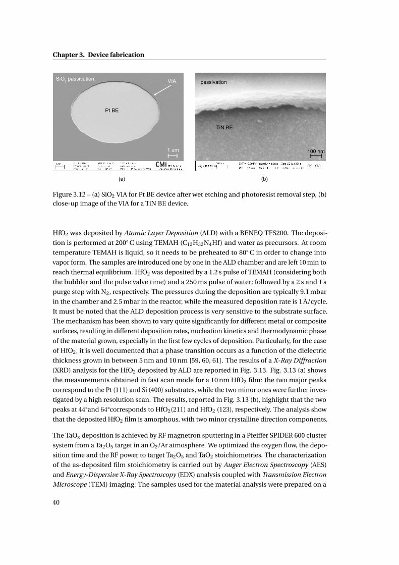
Chapter 3. Device fabrication
Figure 3.12 – (a) SiO2 VIA for Pt BE device after wet etching and photoresist removal step, (b)close-up image of the VIA for a TiN BE device.
HfO2 was deposited by Atomic Layer Deposition (ALD) with a BENEQ TFS200. The deposi-
tion is performed at 200° C using TEMAH (C12H32N4Hf) and water as precursors. At room
temperature TEMAH is liquid, so it needs to be preheated to 80° C in order to change into
vapor form. The samples are introduced one by one in the ALD chamber and are left 10 min to
reach thermal equilibrium. HfO2 was deposited by a 1.2 s pulse of TEMAH (considering both
the bubbler and the pulse valve time) and a 250 ms pulse of water; followed by a 2 s and 1 s
purge step with N2, respectively. The pressures during the deposition are typically 9.1 mbar
in the chamber and 2.5 mbar in the reactor, while the measured deposition rate is 1 Å/cycle.
It must be noted that the ALD deposition process is very sensitive to the substrate surface.
The mechanism has been shown to vary quite significantly for different metal or composite
surfaces, resulting in different deposition rates, nucleation kinetics and thermodynamic phase
of the material grown, especially in the first few cycles of deposition. Particularly, for the case
of HfO2, it is well documented that a phase transition occurs as a function of the dielectric
thickness grown in between 5 nm and 10 nm [59, 60, 61]. The results of a X-Ray Diffraction
(XRD) analysis for the HfO2 deposited by ALD are reported in Fig. 3.13. Fig. 3.13 (a) shows
the measurements obtained in fast scan mode for a 10 nm HfO2 film: the two major peaks
correspond to the Pt (111) and Si (400) substrates, while the two minor ones were further inves-
tigated by a high resolution scan. The results, reported in Fig. 3.13 (b), highlight that the two
peaks at 44°and 64°corresponds to HfO2(211) and HfO2 (123), respectively. The analysis show
that the deposited HfO2 film is amorphous, with two minor crystalline direction components.
The TaOx deposition is achieved by RF magnetron sputtering in a Pfeiffer SPIDER 600 cluster
system from a Ta2O5 target in an O2/Ar atmosphere. We optimized the oxygen flow, the depo-
sition time and the RF power to target Ta2O5 and TaO2 stoichiometries. The characterization
of the as-deposited film stoichiometry is carried out by Auger Electron Spectroscopy (AES)
and Energy-Dispersive X-Ray Spectroscopy (EDX) analysis coupled with Transmission Electron
Microscope (TEM) imaging. The samples used for the material analysis were prepared on a
40
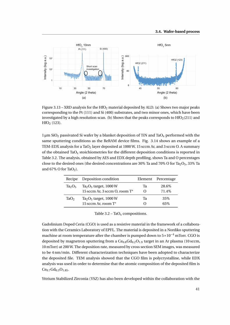
3.4. Wafer-based process
Figure 3.13 – XRD analysis for the HfO2 material deposited by ALD. (a) Shows two major peakscorresponding to the Pt (111) and Si (400) substrates, and two minor ones, which have beeninvestigated by a high resolution scan. (b) Shows that the peaks corresponds to HfO2(211) andHfO2 (123).
1μm SiO2 passivated Si wafer by a blanket deposition of TiN and TaOx performed with the
same sputtering conditions as the ReRAM device films. Fig. 3.14 shows an example of a
TEM-EDX analysis for a TaO2 layer deposited at 1000 W, 15 sccm Ar, and 3 sccm O. A summary
of the obtained TaOx stoichiometries for the different deposition conditions is reported in
Table 3.2. The analysis, obtained by AES and EDX depth profiling, shows Ta and O percentages
close to the desired ones (the desired concentrations are 30% Ta and 70% O for Ta2O5, 33% Ta
and 67% O for TaO2).
Recipe Deposition condition Element Percentage
Ta2O5 Ta2O5 target, 1000 W Ta 28.6%15 sccm Ar, 3 sccm O, room T° O 71.4%
TaO2 Ta2O5 target, 1000 W Ta 35%15 sccm Ar, room T° O 65%
Table 3.2 – TaOx compositions.
Gadolinium Doped Ceria (CGO) is used as a resistive material in the framework of a collabora-
tion with the Ceramics Laboratory of EPFL. The material is deposited in a Nordiko sputtering
machine at room temperature after the chamber is pumped down to 5×10⁻⁴ mTorr. CGO is
deposited by magnetron sputtering from a Ce0.8Gd0.2O1.9 target in an Ar plasma (10 sccm,
10 mTorr) at 200 W. The deposition rate, measured by cross section SEM images, was measured
to be 4 nm/min. Different characterization techniques have been adopted to characterize
the deposited file. TEM analysis showed that the CGO film is polycrystalline, while EDX
analysis was used in order to determine that the atomic composition of the deposited film is
Ce0.7Gd0.3O1.85.
Yttrium Stabilized Zirconia (YSZ) has also been developed within the collaboration with the
41
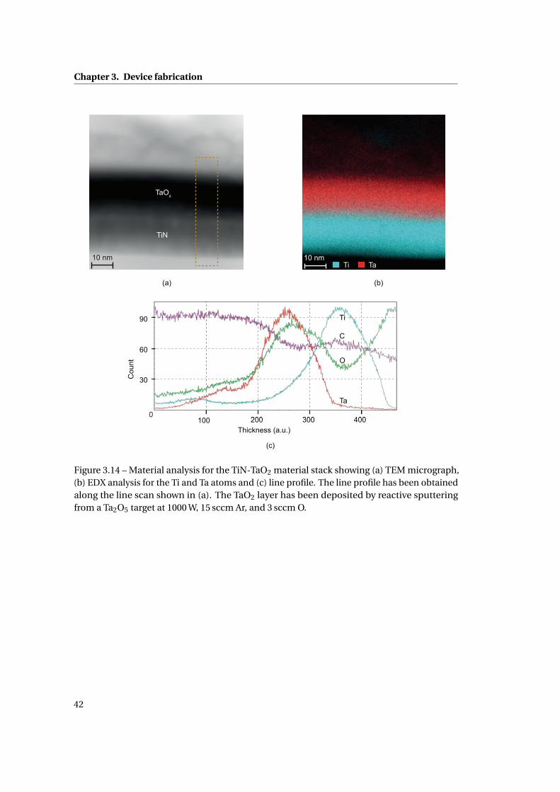
Chapter 3. Device fabrication
Figure 3.14 – Material analysis for the TiN-TaO2 material stack showing (a) TEM micrograph,(b) EDX analysis for the Ti and Ta atoms and (c) line profile. The line profile has been obtainedalong the line scan shown in (a). The TaO2 layer has been deposited by reactive sputteringfrom a Ta2O5 target at 1000 W, 15 sccm Ar, and 3 sccm O.
42
3.4. Wafer-based process
Ceramics Laboratory of EPFL. The material is deposited in a Nordiko sputtering machine at
room temperature from a base pressure of 5×10⁻⁴ mTorr. YSZ is deposited by magnetron
sputtering from a (Y2O3)0.08/(ZrO2)0.92 target in an Ar plasma (30 sccm, 15 mTorr) at 200 W.
The deposition rate is 5 nm/min. EDX analysis on the deposited samples showed an atomic
composition of 68.66% O, 23.32% Zr and 4.10% Y.
3.4.9 Buffer layer and top electrode deposition
Different materials have been tested as buffer layers in between the switching oxide and the
electrodes. In detail, we deposited Ti, Ta, Ni, Al, Hf and Al2O3. The depositions of Ti, Ta, Ni and
Al are obtained with an Alliance-Concept DP 650 sputtering machine, the Hf deposition with
a Balzers BAS 450 multi-target cluster sputtering system, and the Al2O3 by ALD in a BENEQ
TFS200 machine.
The Ti deposition is performed by DC sputtering at room temperature. Before deposition the
chamber is pumped to a high vacuum (1×10⁻⁶ mbar). The Ti target is set quite far from the
wafer (80 mm), in order to ensure a good deposition uniformity and a slower deposition rate.
The plasma is generated by 30 sccm Ar gas at 5×10⁻³ mbar and 400 W. The deposition rate,
measured on a test sample by profilometer, is 3.503 Å/s.
The Ta deposition is realized by DC sputtering at room temperature. The Ta target is set at
80 mm from the substrate, and the chamber base pressure is at high vacuum. The plasma is
generated by 30 sccm Ar gas at 5×10⁻³ mbar and 200 W. The deposition rate, calibrated from
the CMI staff, is 2.9 Å/s.
The Ni deposition is performed by RF sputtering at room temperature. The Ni target is set
at 80 mm from the substrate, and, before the deposition, the chamber is at high vacuum.
The plasma is generated by 30 sccm Ar gas at 5×10⁻³ mbar and 300 W. The deposition rate,
measured on a test sample by profilometer, is 3.809 Å/s.
The Al deposition is performed by DC sputtering at room temperature. For this deposition,
the Al target is set at 30 mm from the substrate. This allows obtaining a film with higher
conductivity: even if the chamber is under a high vacuum (1×10⁻⁶ mbar), residuals gases
can react with the Al ions and oxidize them. The oxidized compounds are non metallic, and
their conduction is lower than the pure Al one. In order to limit this effect, the target can be
placed close to the substrate, so that the possibility for oxidation is reduced. A drawback is that
the deposition is less conformal and the deposition rate is faster. For Al, the deposition rate
rises from 5 nm/s to 12 nm/s, while the resistivity drops from 4.88μΩ·cm to 3.7μΩ·cm. For Ni
and Ta we did not implement this solution because there is not an appreciable difference in
conductivity with respect to the target distance. For Ti, the difference in conductivity is about
8%, but, for a close target position, the deposition rate would be too high for the required
film thicknesses. The plasma is generated by 30 sccm Ar gas at 5×10⁻³ mbar and 400 W. The
deposition rate, measured on a test sample by profilometer, is 18.08 Å/s.
43

Chapter 3. Device fabrication
Hf is deposited by RF sputtering from a Hf target at room temperature. Before deposi-
tion, the chamber is pumped down to 2×10⁻⁶ mbar. The plasma is created by Ar (33 sccm,
4.9×10⁻³ mbar) at 500 W, and, before deposition, the target is cleaned for 600 s. The deposition
rate, measured on a test sample by profilometer, is 0.7465 Å/s
Finally, the Al2O3 layer is deposited by ALD. The deposition is performed at 200° C using TMA
(Al(CH3)3) and water as precursors. As for the HfO2 deposition, the samples are introduced
one by one in the ALD chamber and are left 10 min to reach thermal equilibrium. Al2O3 was
deposited with 150 ms pulse of TMA and a 150 ms pulse of water, followed by a 500 s and
750 s purge with N2, respectively. The deposition pressures during the deposition are typically
9.2 mbar in the chamber and 2.3 mbar in the reactor. The deposition rate is 1.25 Å/cycle.
We used mainly two materials for the TE deposition: TiN or W. For both layers, the TE thickness
is fixed to 56 nm. This is thinner than the BE in order to avoid long TE etching resulting in
possible charge up problems. Moreover, the BE pad should be thick enough to withstand the
overetching during the TE RIE.
TiN can be deposited using two machines. The first option is the same as the one used for
the BE (Subsection 3.4.2). A Pfeiffer SPIDER 600 is used to deposit the film by RF magnetron
reactive sputtering from a Ti target with Ar (40 sccm) and N2 (40 sccm) gases in a 1000 W
plasma. The second possibility for the TiN deposition is an Alliance-Concept DP 650 sputtering
machine. A TiN target, placed at 30 mm from the substrate, is sputtered by the plasma
generated by 30 sccm Ar at 5×10⁻³ mbar and an RF power of 200 W. The deposition rate,
measured on a test sample by profilometer, is 1.872 Å/s. The resistivity of the film, obtained by
a four-point measurement resistivity meter, is 2.02×10⁻⁶ Ω·m.
The W deposition is performed with an Alliance-Concept DP 650 sputtering machine by DC
sputtering at room temperature. The W target is set at 80 mm from the substrate, and the
chamber is at high vacuum. The plasma is generated by 30 sccm Ar gas at 5×10⁻³ mbar and
250 W. The deposition rate, measured on a test sample by profilometer, is 3.79 Å/s.
3.4.10 Top electrode lithography and etching
In order to dehydrate the surface before the resist coating, the wafer is heated at 125° C for
5 min.
We then use 2μm of AZ ECI 3027 at 6300 rpm followed by a softbake at 115° C. The exposure
is performed with the same modality described for the BE in the Subsection 3.4.3, with an
exposure time of 12.5 s. As for the BE lithography, after exposure the resist is developed in AZ
726 MIF developer. A hardbake is finally applied to the wafer in order to improve the resist
thermal stability. The measured photoresist thickness, after the development step, is 2.09μm.
The alignment error with respect to the previous mask is below 3μm.
TiN is etched by RIE in a STS Multiplex ICP dry etcher with a plasma composed by Ar (8 sccm),
44
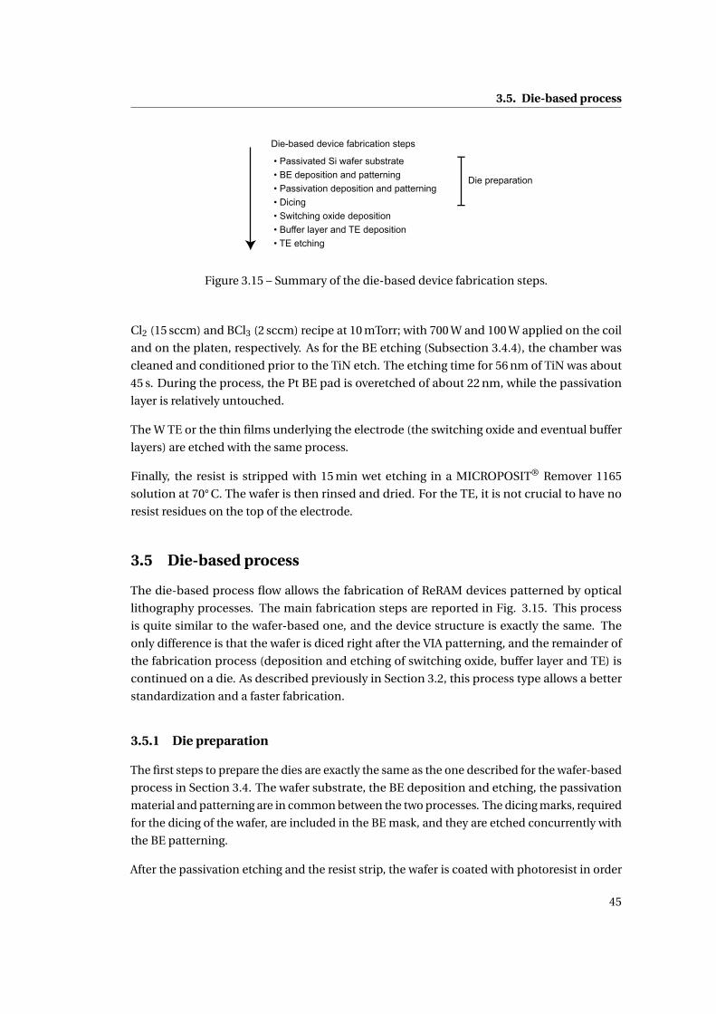
3.5. Die-based process
Figure 3.15 – Summary of the die-based device fabrication steps.
Cl2 (15 sccm) and BCl3 (2 sccm) recipe at 10 mTorr; with 700 W and 100 W applied on the coil
and on the platen, respectively. As for the BE etching (Subsection 3.4.4), the chamber was
cleaned and conditioned prior to the TiN etch. The etching time for 56 nm of TiN was about
45 s. During the process, the Pt BE pad is overetched of about 22 nm, while the passivation
layer is relatively untouched.
The W TE or the thin films underlying the electrode (the switching oxide and eventual buffer
layers) are etched with the same process.
Finally, the resist is stripped with 15 min wet etching in a MICROPOSIT® Remover 1165
solution at 70° C. The wafer is then rinsed and dried. For the TE, it is not crucial to have no
resist residues on the top of the electrode.
3.5 Die-based process
The die-based process flow allows the fabrication of ReRAM devices patterned by optical
lithography processes. The main fabrication steps are reported in Fig. 3.15. This process
is quite similar to the wafer-based one, and the device structure is exactly the same. The
only difference is that the wafer is diced right after the VIA patterning, and the remainder of
the fabrication process (deposition and etching of switching oxide, buffer layer and TE) is
continued on a die. As described previously in Section 3.2, this process type allows a better
standardization and a faster fabrication.
3.5.1 Die preparation
The first steps to prepare the dies are exactly the same as the one described for the wafer-based
process in Section 3.4. The wafer substrate, the BE deposition and etching, the passivation
material and patterning are in common between the two processes. The dicing marks, required
for the dicing of the wafer, are included in the BE mask, and they are etched concurrently with
the BE patterning.
After the passivation etching and the resist strip, the wafer is coated with photoresist in order
45
Chapter 3. Device fabrication
to protect its surface during the dicing process. First, the substrate is dehydrated for 10 min at
120° C, then a 4μm AZ 9207 resist is spun at 1100 rpm, followed by a softbake step at 115° C. AZ
9207 resist is preferred to AZ ECI because of the better adhesion, and the resist is coated as
thick as possible in order to better protect the substrate.
The dicing process is done with a Disco DAD321 automatic dicing saw. The wafer is attached
to a UV tape carrier, and it is subsequently diced with a 100μm thick Ni blade with a rotation
speed of 3000 rpm and a cut speed of 5 mm/s. The cut width is about 100μm, with a misalign-
ment of few tenth of microns. The depth of the cut is calibrated so that the blade dices all the
Si wafer thickness as well as part of the tape (which is about 120μm thick). After dicing, the
UV taped is cured for 2 min under a UV light in order to facilitate the detaching of the 1 cm
×1 cm dies.
3.5.2 Switching oxide, buffer layer and top electrode deposition
Before proceeding with the next process steps, the information to identify each sample is
scribed on the backside of each die. The photoresist used as a protection for the dicing process
is stripped in a 5 min wet etch in acetone [(CH3)2CO] in a sonication bath, followed by a 5 min
rinse in isopropyl alcohol, or IPA [(CH3)2CHOH] and a final clean in deionized water. For the
dies, acetone is preferred to the Remover 1165 solution because it is easier to handle. The IPA
rinse is needed because acetone, due to its low vapor pressure, if not promptly rinsed by IPA
can quickly evaporate and leave behind photoresist redeposition stripes.
The materials, the techniques and the recipes for the switching oxide, buffer layer and TE
deposition are exactly the same as the one described for the wafer-based process. For their
description we therefore refer to Subsection 3.4.8 and Subsection 3.4.9.
3.5.3 Top electrode lithography
In order to dehydrate the surface before the resist coating, the die is heated at 125° C for 10 min.
The photoresist coating is performed with a manual coater. We spun 1μm AZ ECI 3007 first
at 500 rpm with an acceleration of 250 rpm/s for 5 s in order to distribute the resist, then at
2000 rpm with an acceleration of 500 rpm/s for 45 s to complete the coating procedure. The die
is then baked at 90° C for 60 s. The measured photoresist thickness, after the development step,
is 907 nm. The main drawback of coating small substrates is that resist may accumulate at the
edge of the die for several times the nominal thickness. Normally, on wafers, it is possible to
overcome this issue by an Edge Bead Removal (EBR) step which normally uses chemicals to
remove the resist on the edges of the sample. For small dies this is not possible, because of the
shape and the size of the substrate. The resist accumulated on the edge of the die can be too
thick to be exposed at the nominal dose, and it can contaminate or stick to the mask during
the exposure.
46
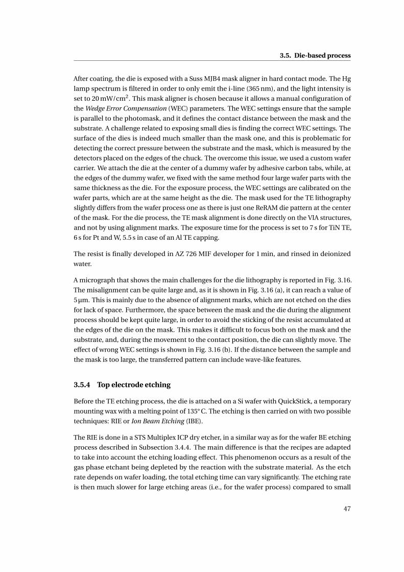
3.5. Die-based process
After coating, the die is exposed with a Suss MJB4 mask aligner in hard contact mode. The Hg
lamp spectrum is filtered in order to only emit the i-line (365 nm), and the light intensity is
set to 20 mW/cm2. This mask aligner is chosen because it allows a manual configuration of
the Wedge Error Compensation (WEC) parameters. The WEC settings ensure that the sample
is parallel to the photomask, and it defines the contact distance between the mask and the
substrate. A challenge related to exposing small dies is finding the correct WEC settings. The
surface of the dies is indeed much smaller than the mask one, and this is problematic for
detecting the correct pressure between the substrate and the mask, which is measured by the
detectors placed on the edges of the chuck. The overcome this issue, we used a custom wafer
carrier. We attach the die at the center of a dummy wafer by adhesive carbon tabs, while, at
the edges of the dummy wafer, we fixed with the same method four large wafer parts with the
same thickness as the die. For the exposure process, the WEC settings are calibrated on the
wafer parts, which are at the same height as the die. The mask used for the TE lithography
slightly differs from the wafer process one as there is just one ReRAM die pattern at the center
of the mask. For the die process, the TE mask alignment is done directly on the VIA structures,
and not by using alignment marks. The exposure time for the process is set to 7 s for TiN TE,
6 s for Pt and W, 5.5 s in case of an Al TE capping.
The resist is finally developed in AZ 726 MIF developer for 1 min, and rinsed in deionized
water.
A micrograph that shows the main challenges for the die lithography is reported in Fig. 3.16.
The misalignment can be quite large and, as it is shown in Fig. 3.16 (a), it can reach a value of
5μm. This is mainly due to the absence of alignment marks, which are not etched on the dies
for lack of space. Furthermore, the space between the mask and the die during the alignment
process should be kept quite large, in order to avoid the sticking of the resist accumulated at
the edges of the die on the mask. This makes it difficult to focus both on the mask and the
substrate, and, during the movement to the contact position, the die can slightly move. The
effect of wrong WEC settings is shown in Fig. 3.16 (b). If the distance between the sample and
the mask is too large, the transferred pattern can include wave-like features.
3.5.4 Top electrode etching
Before the TE etching process, the die is attached on a Si wafer with QuickStick, a temporary
mounting wax with a melting point of 135° C. The etching is then carried on with two possible
techniques: RIE or Ion Beam Etching (IBE).
The RIE is done in a STS Multiplex ICP dry etcher, in a similar way as for the wafer BE etching
process described in Subsection 3.4.4. The main difference is that the recipes are adapted
to take into account the etching loading effect. This phenomenon occurs as a result of the
gas phase etchant being depleted by the reaction with the substrate material. As the etch
rate depends on wafer loading, the total etching time can vary significantly. The etching rate
is then much slower for large etching areas (i.e., for the wafer process) compared to small
47
Chapter 3. Device fabrication
Figure 3.16 – Micrograph of the TE after the TiN etching: (a) shows the misalignment for a10μm VIA device, which is about 5 um, (b) shows the effects of wrong WEC settings for a 2μmdevice.
etching areas (i.e., the die process). As an example, the TiN etching (Ar/Cl2/BCl3 8/15/2 sccm,
10 mTorr, 700 W and 100 W on the coil and on the plated) has an etching time of 3 min for
the wafer process, while it takes less than 50 s if it is performed on a die. Additionally, if we
consider that the TE is generally much thinner than the BE, this process would lead to an
etching time for a 40 nm thick TiN of less than 10 s. Because of these reasons, the power of
the etching recipe is decreased: the TiN etching recipe is then Ar/Cl2/BCl3 at 8/15/2 sccm and
10 mTorr, with a power of 350 W and 50 W on the coil and on the plated. The etching time is
1 min 15 s for the 56 nm TiN TE, while it takes 1 min 45 s to etch 56 nm TiN capped with 66 nm
of Al. During the process, the Pt BE pad is overetched of about 22 nm, while the passivation
layer is relatively untouched. As for the BE etching, the process time increases about 5-10 s for
each consecutive etch. The W TE (62 nm) is etched with SF6 gas at 50 sccm and 5 mTorr with
800 W on the coil and 100 W on the platen. The etching time for the process is 20 s.
An issue related to the die etching is the charging effect. Because the die is not electrically
connected to the substrate (the QuickStick is a poor electrical conductor), and because the
plasma density can be very high with respect to the etching surface, it is possible to damage
the switching oxide during the TE etching. This is especially valid for recipes with a very high
etching rate. For example, a large number of the ReRAM cells measured after the Ar/Cl2/BCl3
at 700 W and 100 W etching were formless, i.e., the pristine resistance state was low. The
interaction of the TE with the charged plasma can indeed build up a potential difference
between the TE and the BE, which, if it is high enough, can induce a breakdown in the
switching oxide. During the electrical characterizations, we observed a clear relation between
a low pristine resistance state and the etching time and power. It is then really important to use
a fixed etching recipe for all the samples and to have a good control of the chamber conditions
before the etching process (using the clean and conditioning process steps presented before).
The IBE is done in a Veeco Nexus IBE350 ion beam etcher with an Ar source. First, the machine
is warmed up with a 5 min etching on a Si dummy wafer. The plasma is generated by a
48
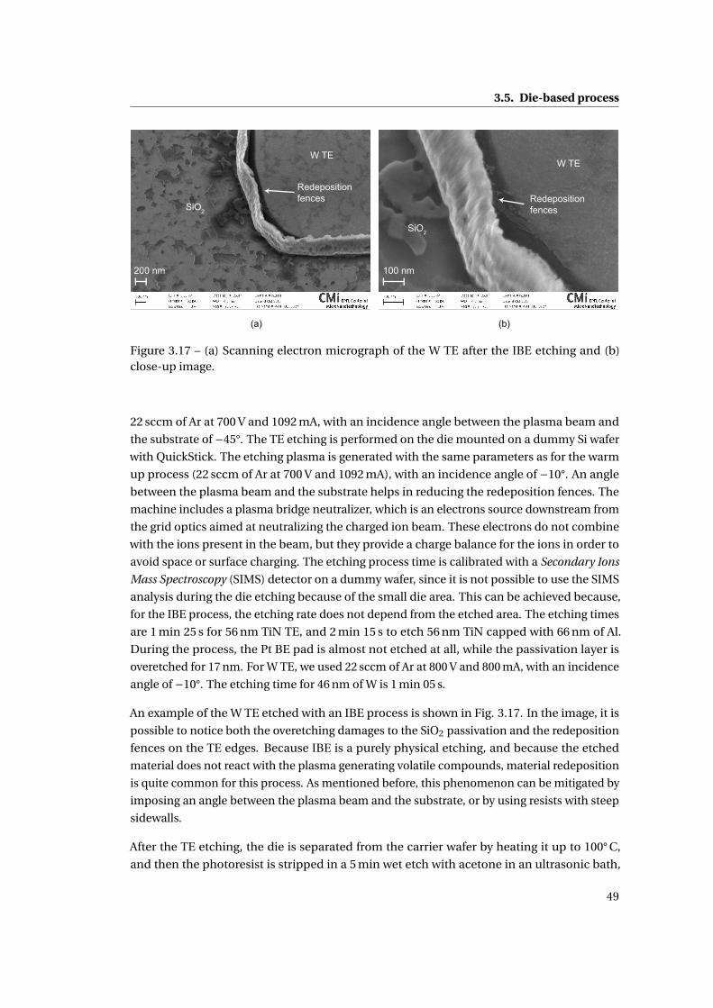
3.5. Die-based process
Figure 3.17 – (a) Scanning electron micrograph of the W TE after the IBE etching and (b)close-up image.
22 sccm of Ar at 700 V and 1092 mA, with an incidence angle between the plasma beam and
the substrate of −45°. The TE etching is performed on the die mounted on a dummy Si wafer
with QuickStick. The etching plasma is generated with the same parameters as for the warm
up process (22 sccm of Ar at 700 V and 1092 mA), with an incidence angle of −10°. An angle
between the plasma beam and the substrate helps in reducing the redeposition fences. The
machine includes a plasma bridge neutralizer, which is an electrons source downstream from
the grid optics aimed at neutralizing the charged ion beam. These electrons do not combine
with the ions present in the beam, but they provide a charge balance for the ions in order to
avoid space or surface charging. The etching process time is calibrated with a Secondary Ions
Mass Spectroscopy (SIMS) detector on a dummy wafer, since it is not possible to use the SIMS
analysis during the die etching because of the small die area. This can be achieved because,
for the IBE process, the etching rate does not depend from the etched area. The etching times
are 1 min 25 s for 56 nm TiN TE, and 2 min 15 s to etch 56 nm TiN capped with 66 nm of Al.
During the process, the Pt BE pad is almost not etched at all, while the passivation layer is
overetched for 17 nm. For W TE, we used 22 sccm of Ar at 800 V and 800 mA, with an incidence
angle of −10°. The etching time for 46 nm of W is 1 min 05 s.
An example of the W TE etched with an IBE process is shown in Fig. 3.17. In the image, it is
possible to notice both the overetching damages to the SiO2 passivation and the redeposition
fences on the TE edges. Because IBE is a purely physical etching, and because the etched
material does not react with the plasma generating volatile compounds, material redeposition
is quite common for this process. As mentioned before, this phenomenon can be mitigated by
imposing an angle between the plasma beam and the substrate, or by using resists with steep
sidewalls.
After the TE etching, the die is separated from the carrier wafer by heating it up to 100° C,
and then the photoresist is stripped in a 5 min wet etch with acetone in an ultrasonic bath,
49

Chapter 3. Device fabrication
followed by a 5 min rinse in IPA and a final cleaning in deionized water.
3.6 Shadow mask-based process
The shadow mask process flow allows the fabrication of ReRAM devices with the TE patterned
directly by the shadow mask. The first part of the process, up to the VIA opening, is performed
on a wafer, which is subsequently diced. The process finishes then on a die by using a shadow
mask-assisted process. The device structure and the masks are different with respect to the
wafer or die process ones. The mask layout for the shadow mask die is shown in Fig. 3.18
(a). The devices have a common BE that extends through all the 1 cm×1 cm die. The BE is
accessible from an opening of the device passivation which lies on top of it. The passivation
is opened to form several VIAs, which, as for the wafer and die processes, have a diameter of
1.5μm, 2μm, 3μm, 5μm and 10μm. The TEs, which measure 300μm × 300μm, are placed on
top of the VIAs. The probes for the electric testing are then connected on the common BE
and on the TE. As mentioned before, the TE is deposited on the dies by means of a shadow
mask, as shown in Fig. 3.18 (b). A schematization of the final device, highlighting its main
components, is shown in Fig. 3.18 (c).
3.6.1 Shadow mask fabrication
The shadow mask used to pattern the TE is fabricated by the fabrication steps summarized in
Fig. 3.19. The Si substrate is similar to the one used for the ReRAM devices. The only difference
is that the shadow mask substrate is not passivated with SiO2.
Before the lithography used to pattern the shadow mask, the wafer surface is treated with
HMDS in vapor phase at 125° C for 10 s. This surface preparation step is needed to ensure a
correct adhesion of the resist to the substrate. We then spincoat 8μm of AZ9260 at 2800 rpm
for 1 min with an automatic coater. The wafer is then softbacked at 115° C for 3 min. The actual
resist thickness, measured by a profilometer, is 8.2μm. The wafer is exposed with a Heidelberg
MLA150 direct LASER writer. The system uses a 405 nm laser diode, achieving a minimum
feature size of 1μm and an alignment accuracy below 500 nm. The resist is exposed with a
dose of 300mJ/cm2 and with a defocus of 1.8μm. Finally, the resist is developed in a AZ9260
developer.
Prior to the shadow mask etching, the resist is exposed to a 20 s O plasma etching (200 sccm
O2, 0.5 mbar, 200 W) in order to remove the non developed photoresist residuals. This step
remove about 100 nm of the photoresist layer. Finally, the substrate is hardbacked at 88 C
for 7 h 30 min. A hardbake is performed in order to increase the thermal, chemical, and
physical stability of developed resist structures in order to withstand the following dry etching.
Without this backing step, the resist would harden excessively when exposed to a long plasma
etching, becoming almost impossible to be stripped away. The resist, after the bake, reduces
its thickness to 8.06 nm mainly due to the solvent evaporation and the resist reflow.
50
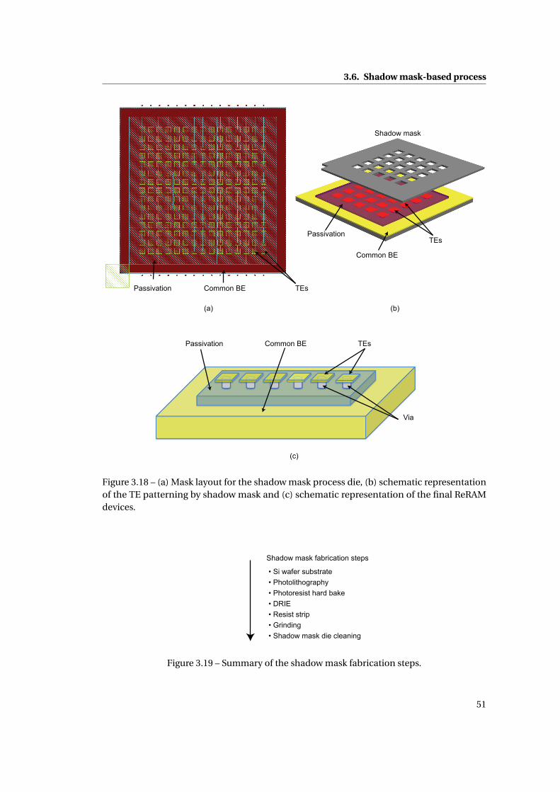
3.6. Shadow mask-based process
Figure 3.18 – (a) Mask layout for the shadow mask process die, (b) schematic representationof the TE patterning by shadow mask and (c) schematic representation of the final ReRAMdevices.
Figure 3.19 – Summary of the shadow mask fabrication steps.
51
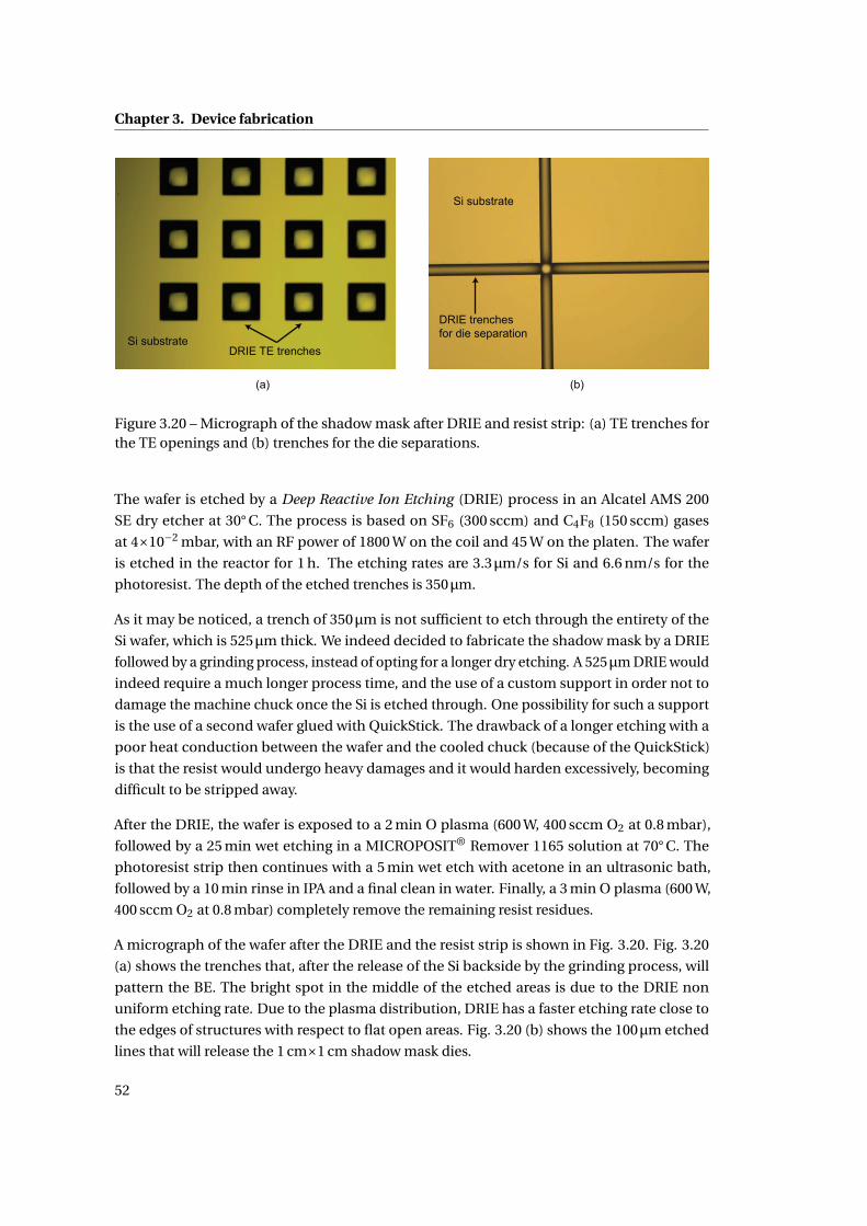
Chapter 3. Device fabrication
Figure 3.20 – Micrograph of the shadow mask after DRIE and resist strip: (a) TE trenches forthe TE openings and (b) trenches for the die separations.
The wafer is etched by a Deep Reactive Ion Etching (DRIE) process in an Alcatel AMS 200
SE dry etcher at 30° C. The process is based on SF6 (300 sccm) and C4F8 (150 sccm) gases
at 4×10⁻² mbar, with an RF power of 1800 W on the coil and 45 W on the platen. The wafer
is etched in the reactor for 1 h. The etching rates are 3.3μm/s for Si and 6.6 nm/s for the
photoresist. The depth of the etched trenches is 350μm.
As it may be noticed, a trench of 350μm is not sufficient to etch through the entirety of the
Si wafer, which is 525μm thick. We indeed decided to fabricate the shadow mask by a DRIE
followed by a grinding process, instead of opting for a longer dry etching. A 525μm DRIE would
indeed require a much longer process time, and the use of a custom support in order not to
damage the machine chuck once the Si is etched through. One possibility for such a support
is the use of a second wafer glued with QuickStick. The drawback of a longer etching with a
poor heat conduction between the wafer and the cooled chuck (because of the QuickStick)
is that the resist would undergo heavy damages and it would harden excessively, becoming
difficult to be stripped away.
After the DRIE, the wafer is exposed to a 2 min O plasma (600 W, 400 sccm O2 at 0.8 mbar),
followed by a 25 min wet etching in a MICROPOSIT® Remover 1165 solution at 70° C. The
photoresist strip then continues with a 5 min wet etch with acetone in an ultrasonic bath,
followed by a 10 min rinse in IPA and a final clean in water. Finally, a 3 min O plasma (600 W,
400 sccm O2 at 0.8 mbar) completely remove the remaining resist residues.
A micrograph of the wafer after the DRIE and the resist strip is shown in Fig. 3.20. Fig. 3.20
(a) shows the trenches that, after the release of the Si backside by the grinding process, will
pattern the BE. The bright spot in the middle of the etched areas is due to the DRIE non
uniform etching rate. Due to the plasma distribution, DRIE has a faster etching rate close to
the edges of structures with respect to flat open areas. Fig. 3.20 (b) shows the 100μm etched
lines that will release the 1 cm×1 cm shadow mask dies.
52

3.7. E-beam lithography process
Figure 3.21 – Summary of the shadow mask-based device fabrication steps.
The backside of the wafer is finally ground for 200μm in order to open the shadow mask
trenches, releasing the TE openings and the dies. Finally, the shadow mask dies are rinsed in
IPA and deionized water.
3.6.2 Die preparation and device fabrication
The shadow mask-based device fabrication steps are summarized in Fig. 3.21. The processes
for the die preparation are exactly the same as the one for the die-based process reported
in Subsection 3.5.1. The different mask used for defining the common BE does not have an
impact on the other process parameters.
The switching oxide deposition is carried on the dies in the same way as for the die-based
process (Subsection 3.5.2). Before the metal depositions, the shadow mask needs to be applied
to the die. The die is placed on a dummy Si wafer, and the shadow mask is placed on it. The
two are then secured with Kapton tape dots. The alignment of the shadow mask is performed
manually, and the alignment is checked by an optical microscope. The large size of the TE is
needed to compensate the alignment error, which can be about 100μm.
The buffer layer and the TE depositions are then performed with the same recipes reported for
the wafer (Subsection 3.4.9) and die processes (Subsection 3.5.2). Finally, the shadow mask is
removed and the devices are ready for testing.
3.7 E-beam lithography process
The e-beam process flow allows the fabrication of nm-scale ReRAM devices patterned by
e-beam lithography. Two different approaches for the process development were applied.
In the first one, the nano-patterning is based on an all-positive resist approach. The second
approach features different resist tones and a different BE pattering, resulting in an improved
device miniaturization.
The two e-beam processes include, on the same wafer, both VIA and crosspoint ReRAMs. As
reported in Section 3.1, for crossbar ReRAMs the device area is defined by the crossing of the
53
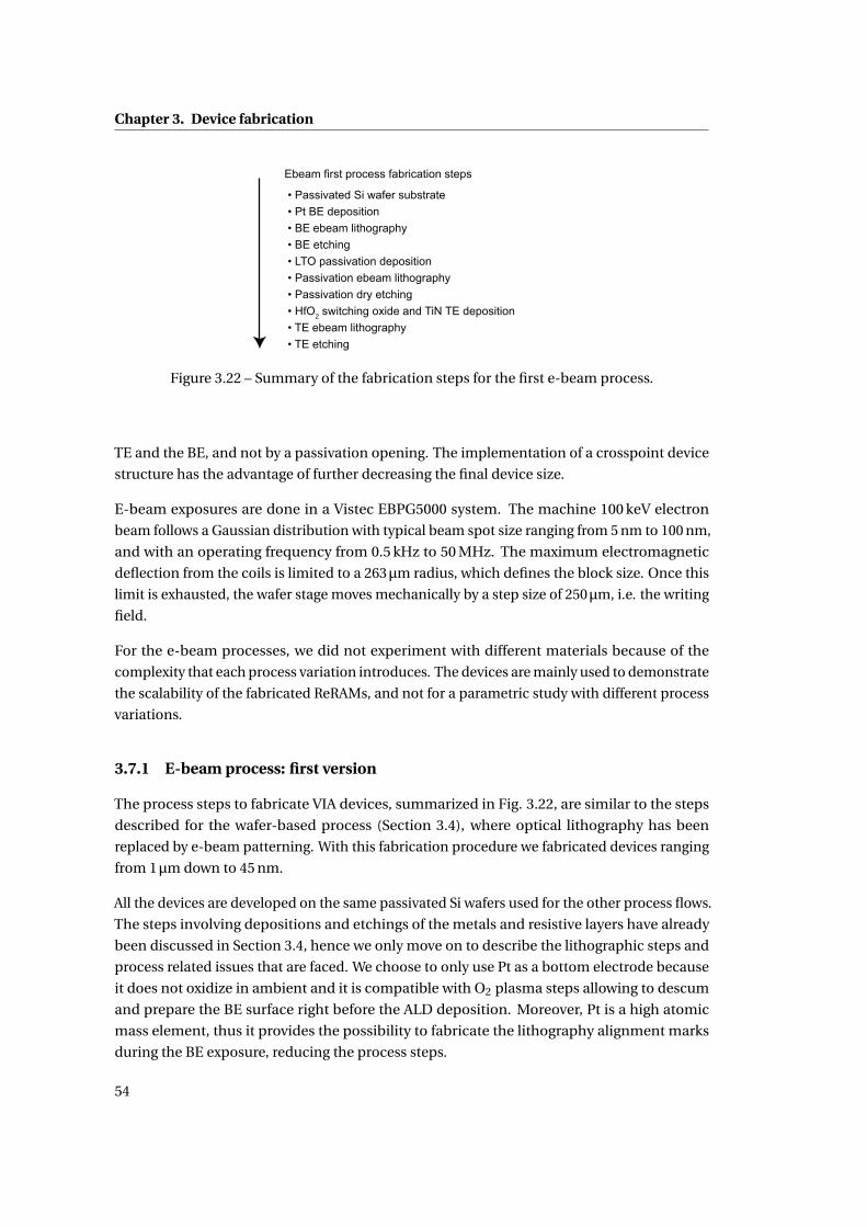
Chapter 3. Device fabrication
Figure 3.22 – Summary of the fabrication steps for the first e-beam process.
TE and the BE, and not by a passivation opening. The implementation of a crosspoint device
structure has the advantage of further decreasing the final device size.
E-beam exposures are done in a Vistec EBPG5000 system. The machine 100 keV electron
beam follows a Gaussian distribution with typical beam spot size ranging from 5 nm to 100 nm,
and with an operating frequency from 0.5 kHz to 50 MHz. The maximum electromagnetic
deflection from the coils is limited to a 263μm radius, which defines the block size. Once this
limit is exhausted, the wafer stage moves mechanically by a step size of 250μm, i.e. the writing
field.
For the e-beam processes, we did not experiment with different materials because of the
complexity that each process variation introduces. The devices are mainly used to demonstrate
the scalability of the fabricated ReRAMs, and not for a parametric study with different process
variations.
3.7.1 E-beam process: first version
The process steps to fabricate VIA devices, summarized in Fig. 3.22, are similar to the steps
described for the wafer-based process (Section 3.4), where optical lithography has been
replaced by e-beam patterning. With this fabrication procedure we fabricated devices ranging
from 1μm down to 45 nm.
All the devices are developed on the same passivated Si wafers used for the other process flows.
The steps involving depositions and etchings of the metals and resistive layers have already
been discussed in Section 3.4, hence we only move on to describe the lithographic steps and
process related issues that are faced. We choose to only use Pt as a bottom electrode because
it does not oxidize in ambient and it is compatible with O2 plasma steps allowing to descum
and prepare the BE surface right before the ALD deposition. Moreover, Pt is a high atomic
mass element, thus it provides the possibility to fabricate the lithography alignment marks
during the BE exposure, reducing the process steps.
54
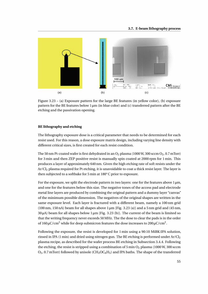
3.7. E-beam lithography process
Figure 3.23 – (a) Exposure pattern for the large BE features (in yellow color), (b) exposurepattern for the BE features below 1μm (in blue color) and (c) transferred pattern after the BEetching and the passivation opening.
BE lithography and etching
The lithography exposure dose is a critical parameter that needs to be determined for each
resist used. For this reason, a dose exposure matrix design, including varying line density with
different critical sizes, is first created for each resist condition.
The 50 nm Pt-coated wafer is first dehydrated in an O2 plasma (1000 W, 300 sccm O2, 0.7 mTorr)
for 3 min and then ZEP positive resist is manually spin coated at 2000 rpm for 1 min. This
produces a layer of approximately 640 nm. Given the high etching rate of soft resists under the
Ar/Cl2 plasma required for Pt etching, it is unavoidable to coat a thick resist layer. The layer is
then subjected to a softbake for 5 min at 180° C prior to exposure.
For the exposure, we split the electrode pattern in two layers: one for the features above 1μm,
and one for the features below this size. The negative tones of the access pad and electrode
metal line layers are produced by combining the original pattern and a dummy layer “canvas”
of the minimum possible dimension. The negatives of the original shapes are written in the
same exposure level. Each layer is fractured with a different beam, namely a 100 nm grid
(100 nm, 150 nA) beam for all shapes above 1μm [Fig. 3.23 (a)] and a 5 nm grid and (45 nm,
30μA) beam for all shapes below 1μm [Fig. 3.23 (b)]. The current of the beam is limited so
that the writing frequency never exceeds 50 MHz. The the dose to clear the pads is in the order
of 160μC/cm2 while for deep submicron features the dose increases to 200μC/cm2.
Following the exposure, the resist is developed for 1 min using a 90:10 MiBK:IPA solution,
rinsed in IPA (1 min) and dried using nitrogen gun. The BE etching is performed under Ar/Cl2
plasma recipe, as described for the wafer process BE etching in Subsection 3.4.4. Following
the etching, the resist is stripped using a combination of 5 min O2 plasma (1000 W, 300 sccm
O2, 0.7 mTorr) followed by anisole (CH3OC6H5) and IPA baths. The shape of the transferred
55

Chapter 3. Device fabrication
patterns is reported in Fig. 3.23.
On this lithographic level a 29×29 Pre Alignment Marker (PAM) array and four (three global
and a keystone) 3×3 negative alignment marker arrays comprising of 20μm×20μm square
marks are created. Field centering is applied to minimize stitching errors.
Because of the use of a positive tone resist, it was not possible to achieve a high resolution in
the BE pattering. This means that the BE metal line features cannot be well controlled, thus
the crosspoint devices, for this version of the e-beam process, are not going to be well defined.
Passivation lithography and etching
After deposition of the 100 nm LTO passivation layer, the second lithographic level is patterned
in the same fashion. Positive ZEP resist is spincoated at 4000 rpm resulting in a 120 nm layer
coated. VIAs with critical dimension from 1μm down to 45 nm are patterned. The pads are
released using a 100 nm grid and a 150 nA beam (100 nm), while the VIAs are patterned with a
5 nm grid, and 15 nA beam (5 nm). An alignment protocol is performed by centering the VIAs
on their respective electrodes. The strategy to determine the optimal dose is the same as for
the BE.
The nanoscale etching of the LTO VIAs cannot be reliably performed with BHF solution, such as
for the other process flows. The bath local pH variations and flow as well as the etching kinetics
in nanoscale dimensions result in a rather unpredictable etching behavior and significant
differences between the etching times between micron to deep nano scale dimensions. For
this reason the LTO layer is etched using a RIE with He/C4F8 gases in a SPTS APS dielectric
etcher. Finally, the resist is stripped by a combination of 5 min O2 plasma (1000 W, 300 sccm
O2, 0.7 mTorr) followed by anisole and IPA baths. An example of the passivation etching result
is shown in Fig. 3.23. A 780 nm VIA with the Pt TE is shown in Fig. 3.24 (a), while a 45 nm LTO
VIA opening is reported in Fig. 3.23 (b).
For the crosspoint device part of the wafer, the resist is simply removed from the device area,
so that the passivation is completely etched away.
Oxide and TE deposition and etching
After the passivation opening, 5 nm of HfO2 and 50 nm of TiN are deposited. The Pt metal
markers are now covered with LTO (100 nm), HfO2 (5 nm) and TiN (50 nm). Whereas the LTO
layer does not significantly decrease the material contrast between Pt and substrate under a
100 kV beam, the TiN deposition dramatically lower the contrast for determining the alignment
markers, resulting in the failure of the top level alignment. The contrast loss is possibly owed
to the overall deposited thickness (~150 nm) exceeding by far that of the Pt layer (50 nm). To
circumvent that, we add an additional photolithographic layer on top of the marker sites
followed by a TiN dry etch step to remove some of the TiN and oxide materials. Following that,
56
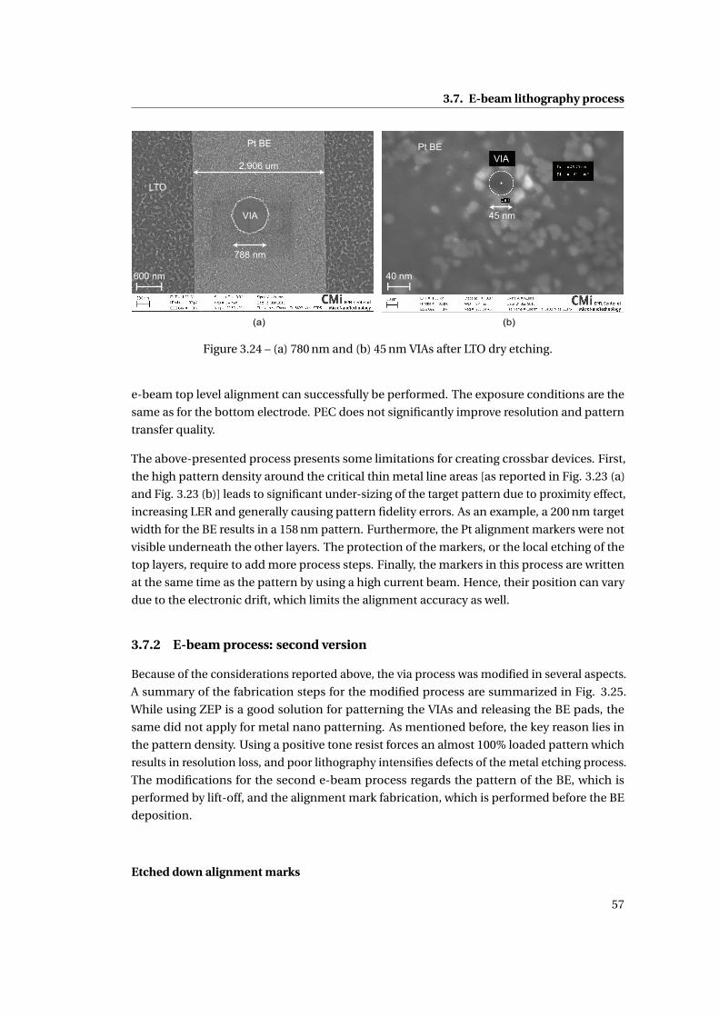
3.7. E-beam lithography process
Figure 3.24 – (a) 780 nm and (b) 45 nm VIAs after LTO dry etching.
e-beam top level alignment can successfully be performed. The exposure conditions are the
same as for the bottom electrode. PEC does not significantly improve resolution and pattern
transfer quality.
The above-presented process presents some limitations for creating crossbar devices. First,
the high pattern density around the critical thin metal line areas [as reported in Fig. 3.23 (a)
and Fig. 3.23 (b)] leads to significant under-sizing of the target pattern due to proximity effect,
increasing LER and generally causing pattern fidelity errors. As an example, a 200 nm target
width for the BE results in a 158 nm pattern. Furthermore, the Pt alignment markers were not
visible underneath the other layers. The protection of the markers, or the local etching of the
top layers, require to add more process steps. Finally, the markers in this process are written
at the same time as the pattern by using a high current beam. Hence, their position can vary
due to the electronic drift, which limits the alignment accuracy as well.
3.7.2 E-beam process: second version
Because of the considerations reported above, the via process was modified in several aspects.
A summary of the fabrication steps for the modified process are summarized in Fig. 3.25.
While using ZEP is a good solution for patterning the VIAs and releasing the BE pads, the
same did not apply for metal nano patterning. As mentioned before, the key reason lies in
the pattern density. Using a positive tone resist forces an almost 100% loaded pattern which
results in resolution loss, and poor lithography intensifies defects of the metal etching process.
The modifications for the second e-beam process regards the pattern of the BE, which is
performed by lift-off, and the alignment mark fabrication, which is performed before the BE
deposition.
Etched down alignment marks
57
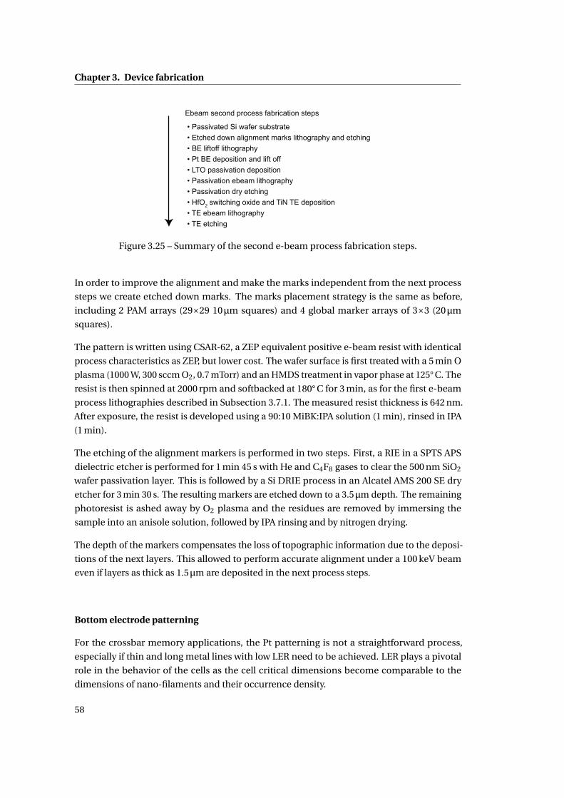
Chapter 3. Device fabrication
Figure 3.25 – Summary of the second e-beam process fabrication steps.
In order to improve the alignment and make the marks independent from the next process
steps we create etched down marks. The marks placement strategy is the same as before,
including 2 PAM arrays (29×29 10μm squares) and 4 global marker arrays of 3×3 (20μm
squares).
The pattern is written using CSAR-62, a ZEP equivalent positive e-beam resist with identical
process characteristics as ZEP, but lower cost. The wafer surface is first treated with a 5 min O
plasma (1000 W, 300 sccm O2, 0.7 mTorr) and an HMDS treatment in vapor phase at 125° C. The
resist is then spinned at 2000 rpm and softbacked at 180° C for 3 min, as for the first e-beam
process lithographies described in Subsection 3.7.1. The measured resist thickness is 642 nm.
After exposure, the resist is developed using a 90:10 MiBK:IPA solution (1 min), rinsed in IPA
(1 min).
The etching of the alignment markers is performed in two steps. First, a RIE in a SPTS APS
dielectric etcher is performed for 1 min 45 s with He and C4F8 gases to clear the 500 nm SiO2
wafer passivation layer. This is followed by a Si DRIE process in an Alcatel AMS 200 SE dry
etcher for 3 min 30 s. The resulting markers are etched down to a 3.5μm depth. The remaining
photoresist is ashed away by O2 plasma and the residues are removed by immersing the
sample into an anisole solution, followed by IPA rinsing and by nitrogen drying.
The depth of the markers compensates the loss of topographic information due to the deposi-
tions of the next layers. This allowed to perform accurate alignment under a 100 keV beam
even if layers as thick as 1.5μm are deposited in the next process steps.
Bottom electrode patterning
For the crossbar memory applications, the Pt patterning is not a straightforward process,
especially if thin and long metal lines with low LER need to be achieved. LER plays a pivotal
role in the behavior of the cells as the cell critical dimensions become comparable to the
dimensions of nano-filaments and their occurrence density.
58

3.7. E-beam lithography process
Several approaches have been taken towards that goal. First, the original pattern and not its
negative is used. In this approach, we used a negative tone HSQ (hydrogen silsequioxane)
6% to pattern the BE. However the completely unreactive Pt surface creates serious adhesion
issues of HSQ on Pt. This results in less than 40% of pattern transfer on the wafer and significant
scumming of the lithographic pattern. The application of surface treatment techniques before
coating, such as plasma O2 , dehydration and HMDS functionalization could not mitigate the
problem.
The second approach relies on a Pt lift-off process based on an MMA (8.5) (methyl methacry-
late) and PMMA [Poly(methyl methacrylate)] positive resist bilayer. The low molecular weight
MMA can easily be solved by acetone whereas the high molecular weight PMMA can sustain
the mechanical stress during the exposure and lithographic processes. First, the wafer surface
is dehydrated and cleaned with a 3 min O2 plasma (1000 W, 300 sccm O2, 0.7 mTorr) followed
by surface functionalization with HMDS adhesion promoter. Second, 150 nm of MMA resist
is spin coated at 4000 rpm. The coated film is then softbaked at 180° C for 5 min to remove
excess moisture from the resist and improve adhesion. PMMA (495k A2) at 50 nm nominal
thickness is then spin-coated at 8000 rpm and baked again at 180° C for 5 min. The target BE
thickness is in the order of 50 nm, so the MMA/PMMA bilayer is engineered to have a 4:1 ratio
with respect to the film thickness to facilitate the lift-off process.
To achieve high alignment accuracy and high resolution a “zero-level” alignment strategy is
followed. First, the pattern is split in two exposure jobs which are performed back to back
in the same lithographic step. In the first exposure, all sub 1μm features are aligned with
respect to the etched down markers already present on wafer and then written using a 5 nm
grid and 20 nA beam. No PEC needs to be applied, and the dose is 4400 μC/cm2. Linearity
error has been characterized and a 5 nm positive bias in the critical dimension direction has
been applied for all sub-100 nm features.
The same concept is used for micron scale features. All micron scale features are proximity
effect corrected (β = 33, η = 0.6). To reduce writing time, a 150 nA beam and 100 nm grid
are used. However, high current beams are affected by electronic drift. In order to eliminate
electronic drift, the beam is loaded two times. In the first run, initial calibrations are performed
and 4 dummy sites are written in the edges of the wafer. This allows enough time for the beam
to stabilize. The beam is loaded anew, an alignment protocol is executed and the features of
interest are written. Writing field centering is applied to all patterns written, and exposure
is done at 1250 μC/cm2 for all features. A solution of 1:3 MIBK:IPA is used to maximize the
developed resist contrast at the expense of an elevated dose to clear, followed by an IPA rinse.
Prior to deposition, the developed resist film is exposed to a short 13 s O2 plasma (1000 W,
300 sccm O2, 0.7 mTorr) in order to clear out any resist residues from the exposed sites. A
10 nm Ti adhesion layer and a 45 nm Pt layer are deposited back to back without breaking
vacuum by Leybold Optics LAB 600H e-beam thermal evaporation. Lift-off is performed in
acetone solution for 4 h, followed by a sonication step to release the final structures.
59
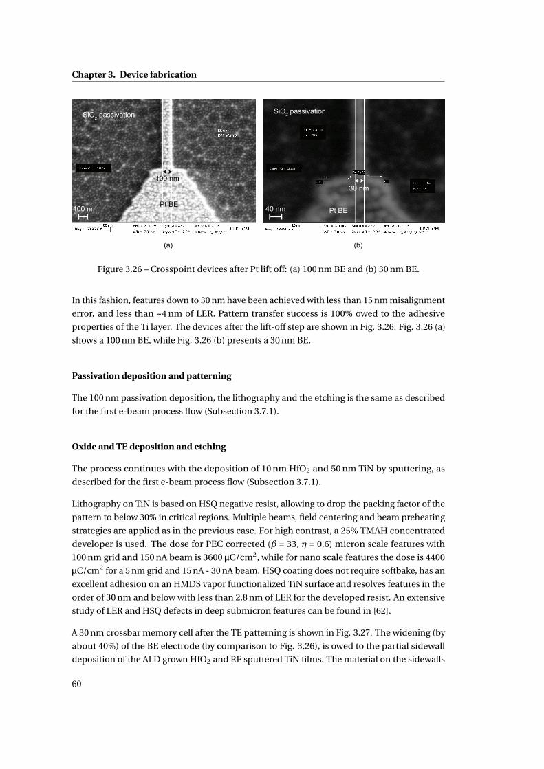
Chapter 3. Device fabrication
Figure 3.26 – Crosspoint devices after Pt lift off: (a) 100 nm BE and (b) 30 nm BE.
In this fashion, features down to 30 nm have been achieved with less than 15 nm misalignment
error, and less than ~4 nm of LER. Pattern transfer success is 100% owed to the adhesive
properties of the Ti layer. The devices after the lift-off step are shown in Fig. 3.26. Fig. 3.26 (a)
shows a 100 nm BE, while Fig. 3.26 (b) presents a 30 nm BE.
Passivation deposition and patterning
The 100 nm passivation deposition, the lithography and the etching is the same as described
for the first e-beam process flow (Subsection 3.7.1).
Oxide and TE deposition and etching
The process continues with the deposition of 10 nm HfO2 and 50 nm TiN by sputtering, as
described for the first e-beam process flow (Subsection 3.7.1).
Lithography on TiN is based on HSQ negative resist, allowing to drop the packing factor of the
pattern to below 30% in critical regions. Multiple beams, field centering and beam preheating
strategies are applied as in the previous case. For high contrast, a 25% TMAH concentrated
developer is used. The dose for PEC corrected (β = 33, η = 0.6) micron scale features with
100 nm grid and 150 nA beam is 3600 μC/cm2, while for nano scale features the dose is 4400
μC/cm2 for a 5 nm grid and 15 nA - 30 nA beam. HSQ coating does not require softbake, has an
excellent adhesion on an HMDS vapor functionalized TiN surface and resolves features in the
order of 30 nm and below with less than 2.8 nm of LER for the developed resist. An extensive
study of LER and HSQ defects in deep submicron features can be found in [62].
A 30 nm crossbar memory cell after the TE patterning is shown in Fig. 3.27. The widening (by
about 40%) of the BE electrode (by comparison to Fig. 3.26), is owed to the partial sidewall
deposition of the ALD grown HfO2 and RF sputtered TiN films. The material on the sidewalls
60
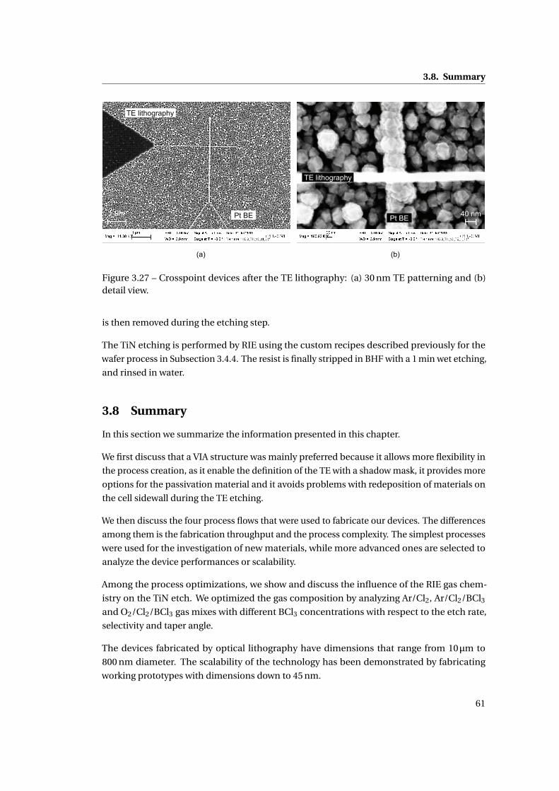
3.8. Summary
Figure 3.27 – Crosspoint devices after the TE lithography: (a) 30 nm TE patterning and (b)detail view.
is then removed during the etching step.
The TiN etching is performed by RIE using the custom recipes described previously for the
wafer process in Subsection 3.4.4. The resist is finally stripped in BHF with a 1 min wet etching,
and rinsed in water.
3.8 Summary
In this section we summarize the information presented in this chapter.
We first discuss that a VIA structure was mainly preferred because it allows more flexibility in
the process creation, as it enable the definition of the TE with a shadow mask, it provides more
options for the passivation material and it avoids problems with redeposition of materials on
the cell sidewall during the TE etching.
We then discuss the four process flows that were used to fabricate our devices. The differences
among them is the fabrication throughput and the process complexity. The simplest processes
were used for the investigation of new materials, while more advanced ones are selected to
analyze the device performances or scalability.
Among the process optimizations, we show and discuss the influence of the RIE gas chem-
istry on the TiN etch. We optimized the gas composition by analyzing Ar/Cl2, Ar/Cl2/BCl3
and O2/Cl2/BCl3 gas mixes with different BCl3 concentrations with respect to the etch rate,
selectivity and taper angle.
The devices fabricated by optical lithography have dimensions that range from 10μm to
800 nm diameter. The scalability of the technology has been demonstrated by fabricating
working prototypes with dimensions down to 45 nm.
61

4 Device characterization: DC analysis
This chapter discusses the electrical data obtained for DC tests. The goal of the analysis
reported hereafter is to show how different process flow variations and device compositions
reflect on the memory electrical characteristics. Moreover, the analyzed data shows insights
about the ReRAM working mechanism and the adopted methodology approach.
The remainder of the chapter is organized as follows. First, in Section 4.1, we highlight the
methodology and the goal of the analysis. Afterward, in Section 4.2, we discuss the factors
analyzed during this study. Then, in Section 4.3 we present some examples from the measured
data, obtained either by forcing a voltage or a current into the device. In Section 4.4, we
discuss the influence of each specific fabrication process variation over the obtained memory
characteristics. Afterward, in Section 4.5, we perform a correlation analysis on the database,
analyzing the features that are common among all the fabricated devices, regardless of the
process differences. The target of this analysis is to highlight the relations that are intrinsic for
ReRAM devices, and to validate the characterization methodology. We then show in Section
4.6 the results obtained from retention tests. Finally, we conclude the chapter with a summary
of the work in Section 4.7.
4.1 DC characterization methodology
We have decided to investigate the factors that influence the ReRAM memory characteristics
with two complementary characterization approaches: DC and pulse tests.
We use DC tests to determine the effects that variations in the fabrication steps, device geome-
try or composition has on the ReRAM electrical behavior. This type of electrical test, discussed
in detail in this chapter, is used to drive the device optimization. The characterization method-
ology is represented in Fig. 4.1. The devices are fabricated with several different process
variations, and they are subsequently tested in DC with a standardized test procedure that is
common for all the devices. After the extraction of the main electrical parameters, the data are
analyzed in order to extract the dependencies of the ReRAM characteristics with respect to the
63
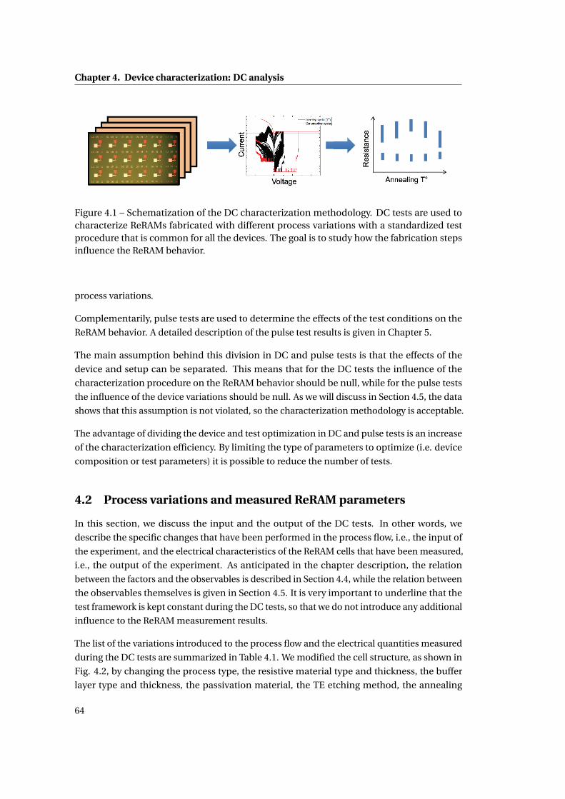
Chapter 4. Device characterization: DC analysis
Figure 4.1 – Schematization of the DC characterization methodology. DC tests are used tocharacterize ReRAMs fabricated with different process variations with a standardized testprocedure that is common for all the devices. The goal is to study how the fabrication stepsinfluence the ReRAM behavior.
process variations.
Complementarily, pulse tests are used to determine the effects of the test conditions on the
ReRAM behavior. A detailed description of the pulse test results is given in Chapter 5.
The main assumption behind this division in DC and pulse tests is that the effects of the
device and setup can be separated. This means that for the DC tests the influence of the
characterization procedure on the ReRAM behavior should be null, while for the pulse tests
the influence of the device variations should be null. As we will discuss in Section 4.5, the data
shows that this assumption is not violated, so the characterization methodology is acceptable.
The advantage of dividing the device and test optimization in DC and pulse tests is an increase
of the characterization efficiency. By limiting the type of parameters to optimize (i.e. device
composition or test parameters) it is possible to reduce the number of tests.
4.2 Process variations and measured ReRAM parameters
In this section, we discuss the input and the output of the DC tests. In other words, we
describe the specific changes that have been performed in the process flow, i.e., the input of
the experiment, and the electrical characteristics of the ReRAM cells that have been measured,
i.e., the output of the experiment. As anticipated in the chapter description, the relation
between the factors and the observables is described in Section 4.4, while the relation between
the observables themselves is given in Section 4.5. It is very important to underline that the
test framework is kept constant during the DC tests, so that we do not introduce any additional
influence to the ReRAM measurement results.
The list of the variations introduced to the process flow and the electrical quantities measured
during the DC tests are summarized in Table 4.1. We modified the cell structure, as shown in
Fig. 4.2, by changing the process type, the resistive material type and thickness, the buffer
layer type and thickness, the passivation material, the TE etching method, the annealing
64
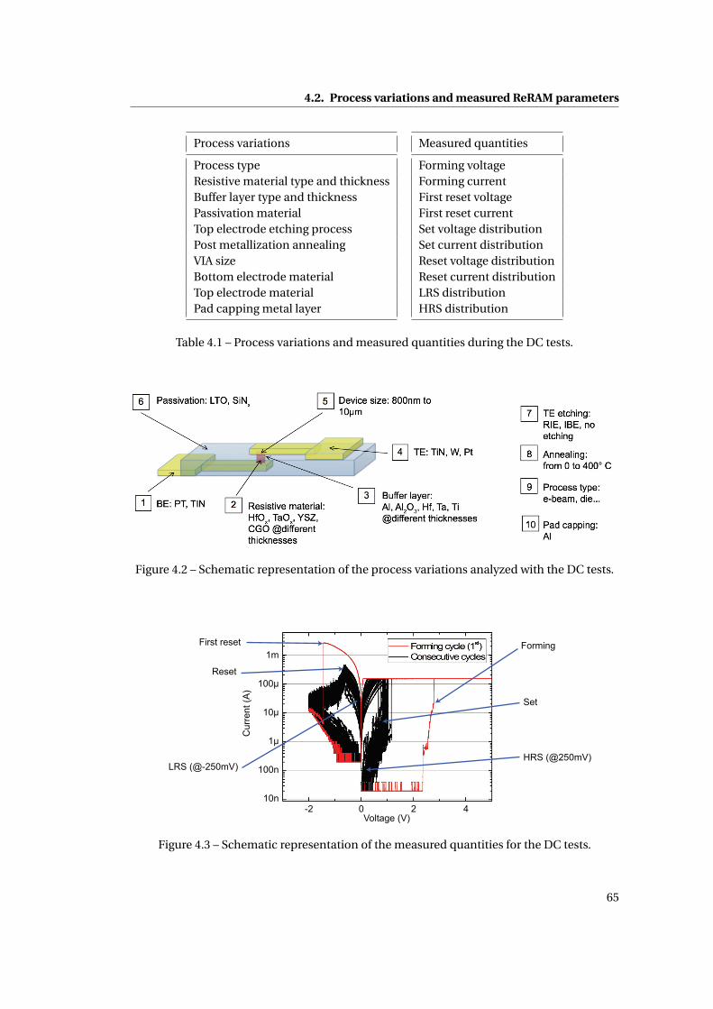
4.2. Process variations and measured ReRAM parameters
Process variations Measured quantities
Process type Forming voltageResistive material type and thickness Forming currentBuffer layer type and thickness First reset voltagePassivation material First reset currentTop electrode etching process Set voltage distributionPost metallization annealing Set current distributionVIA size Reset voltage distributionBottom electrode material Reset current distributionTop electrode material LRS distributionPad capping metal layer HRS distribution
Table 4.1 – Process variations and measured quantities during the DC tests.
Figure 4.2 – Schematic representation of the process variations analyzed with the DC tests.
Figure 4.3 – Schematic representation of the measured quantities for the DC tests.
65
Chapter 4. Device characterization: DC analysis
temperature, the VIA size, the BE, the TE material and the electrode capping layer. The
measured quantities during the DC tests, as shown in Fig. 4.3, are the forming (voltage and
current), the first reset (voltage and current), and the distribution of set (voltage and current),
reset (voltage and current), LRS and HRS.
Because the main target for the process variations was the optimization of the ReRAM char-
acteristics, the experiments are not optimally designed to extract a compact model for the
description of the measured behaviors. For example, we did not test every possible combina-
tion of process variations, and we do not perform the same amount of test for all the specific
ReRAM structures.
In the DC database, we reported more than 230 ReRAMs tests, each one based on 50 DC cycles,
from about 90 different fabrication run. The details of the different process variations are
reported in Table 4.2, in which we show, for each process change, the specific modifications.
This relative high number of tested devices was made possible thanks to the possibility of
sharing the die substrates among different process runs, and because of a highly standardized
measurement and data analysis procedure. The devices with the higher number of tests (about
70) are based on Pt/HfO2 (5 nm)/Ti (3 nm)/TiN, because, according to our data, they have the
better trade off between the measured characteristics.
Process variation First level modification Second level modification
Process typeDie process
Shadow mask process
Resistive material thick-
ness and typeHfO2
3 nm
5 nm
6 nm
10 nm
TaOx
4 min Ta2O5 (45 nm)
45 s TaO2 (25 nm)
1 min 30 s Ta2O5 @500 W (ca.
6.3 nm)1 min Ta2O5 @500 W (ca.
3.7 nm)45 s Ta2O5 @500 W (ca.
2.5 nm)
CGO
3 min
4 min
5 min
YSZ 5 min
66
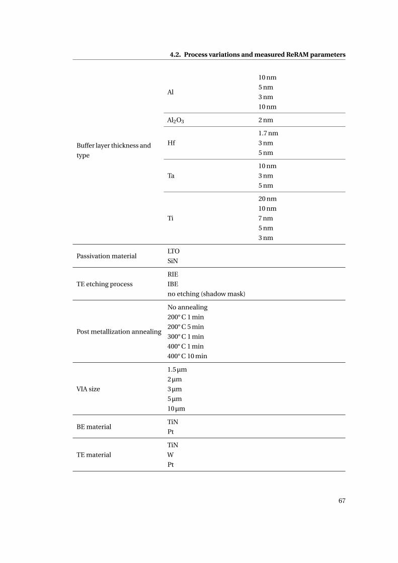
4.2. Process variations and measured ReRAM parameters
Buffer layer thickness and
type
Al
10 nm
5 nm
3 nm
10 nm
Al2O3 2 nm
Hf
1.7 nm
3 nm
5 nm
Ta
10 nm
3 nm
5 nm
Ti
20 nm
10 nm
7 nm
5 nm
3 nm
Passivation materialLTO
SiN
TE etching process
RIE
IBE
no etching (shadow mask)
Post metallization annealing
No annealing
200° C 1 min
200° C 5 min
300° C 1 min
400° C 1 min
400° C 10 min
VIA size
1.5μm
2μm
3μm
5μm
10μm
BE materialTiN
Pt
TE material
TiN
W
Pt
67
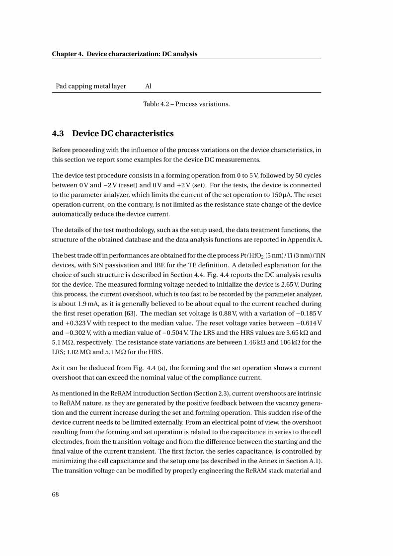
Chapter 4. Device characterization: DC analysis
Pad capping metal layer Al
Table 4.2 – Process variations.
4.3 Device DC characteristics
Before proceeding with the influence of the process variations on the device characteristics, in
this section we report some examples for the device DC measurements.
The device test procedure consists in a forming operation from 0 to 5 V, followed by 50 cycles
between 0 V and −2 V (reset) and 0 V and +2 V (set). For the tests, the device is connected
to the parameter analyzer, which limits the current of the set operation to 150μA. The reset
operation current, on the contrary, is not limited as the resistance state change of the device
automatically reduce the device current.
The details of the test methodology, such as the setup used, the data treatment functions, the
structure of the obtained database and the data analysis functions are reported in Appendix A.
The best trade off in performances are obtained for the die process Pt/HfO2 (5 nm)/Ti (3 nm)/TiN
devices, with SiN passivation and IBE for the TE definition. A detailed explanation for the
choice of such structure is described in Section 4.4. Fig. 4.4 reports the DC analysis results
for the device. The measured forming voltage needed to initialize the device is 2.65 V. During
this process, the current overshoot, which is too fast to be recorded by the parameter analyzer,
is about 1.9 mA, as it is generally believed to be about equal to the current reached during
the first reset operation [63]. The median set voltage is 0.88 V, with a variation of −0.185 V
and +0.323 V with respect to the median value. The reset voltage varies between −0.614 V
and −0.302 V, with a median value of −0.504 V. The LRS and the HRS values are 3.65 kΩ and
5.1 MΩ, respectively. The resistance state variations are between 1.46 kΩ and 106 kΩ for the
LRS; 1.02 MΩ and 5.1 MΩ for the HRS.
As it can be deduced from Fig. 4.4 (a), the forming and the set operation shows a current
overshoot that can exceed the nominal value of the compliance current.
As mentioned in the ReRAM introduction Section (Section 2.3), current overshoots are intrinsic
to ReRAM nature, as they are generated by the positive feedback between the vacancy genera-
tion and the current increase during the set and forming operation. This sudden rise of the
device current needs to be limited externally. From an electrical point of view, the overshoot
resulting from the forming and set operation is related to the capacitance in series to the cell
electrodes, from the transition voltage and from the difference between the starting and the
final value of the current transient. The first factor, the series capacitance, is controlled by
minimizing the cell capacitance and the setup one (as described in the Annex in Section A.1).
The transition voltage can be modified by properly engineering the ReRAM stack material and
68
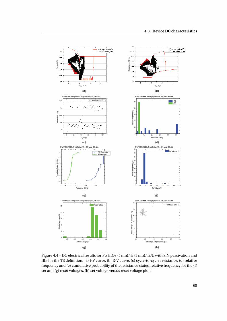
4.3. Device DC characteristics
Figure 4.4 – DC electrical results for Pt/HfO2 (5 nm)/Ti (3 nm)/TiN, with SiN passivation andIBE for the TE definition: (a) I-V curve, (b) R-V curve, (c) cycle-to-cycle resistance, (d) relativefrequency and (e) cumulative probability of the resistance states, relative frequency for the (f)set and (g) reset voltages, (h) set voltage versus reset voltage plot.
69
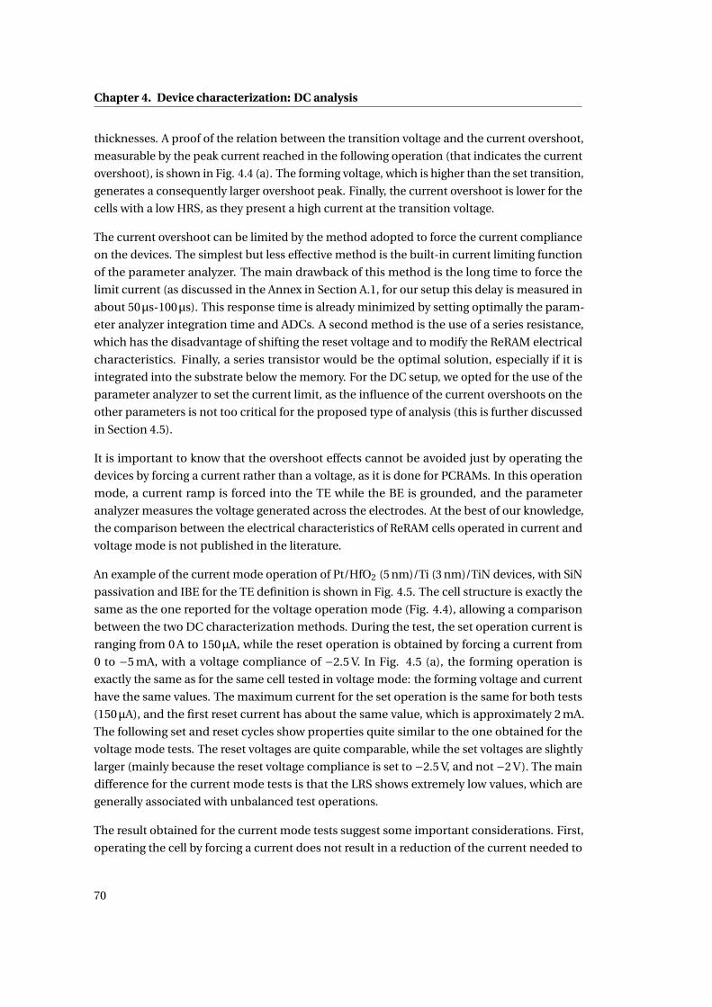
Chapter 4. Device characterization: DC analysis
thicknesses. A proof of the relation between the transition voltage and the current overshoot,
measurable by the peak current reached in the following operation (that indicates the current
overshoot), is shown in Fig. 4.4 (a). The forming voltage, which is higher than the set transition,
generates a consequently larger overshoot peak. Finally, the current overshoot is lower for the
cells with a low HRS, as they present a high current at the transition voltage.
The current overshoot can be limited by the method adopted to force the current compliance
on the devices. The simplest but less effective method is the built-in current limiting function
of the parameter analyzer. The main drawback of this method is the long time to force the
limit current (as discussed in the Annex in Section A.1, for our setup this delay is measured in
about 50μs-100μs). This response time is already minimized by setting optimally the param-
eter analyzer integration time and ADCs. A second method is the use of a series resistance,
which has the disadvantage of shifting the reset voltage and to modify the ReRAM electrical
characteristics. Finally, a series transistor would be the optimal solution, especially if it is
integrated into the substrate below the memory. For the DC setup, we opted for the use of the
parameter analyzer to set the current limit, as the influence of the current overshoots on the
other parameters is not too critical for the proposed type of analysis (this is further discussed
in Section 4.5).
It is important to know that the overshoot effects cannot be avoided just by operating the
devices by forcing a current rather than a voltage, as it is done for PCRAMs. In this operation
mode, a current ramp is forced into the TE while the BE is grounded, and the parameter
analyzer measures the voltage generated across the electrodes. At the best of our knowledge,
the comparison between the electrical characteristics of ReRAM cells operated in current and
voltage mode is not published in the literature.
An example of the current mode operation of Pt/HfO2 (5 nm)/Ti (3 nm)/TiN devices, with SiN
passivation and IBE for the TE definition is shown in Fig. 4.5. The cell structure is exactly the
same as the one reported for the voltage operation mode (Fig. 4.4), allowing a comparison
between the two DC characterization methods. During the test, the set operation current is
ranging from 0 A to 150μA, while the reset operation is obtained by forcing a current from
0 to −5 mA, with a voltage compliance of −2.5 V. In Fig. 4.5 (a), the forming operation is
exactly the same as for the same cell tested in voltage mode: the forming voltage and current
have the same values. The maximum current for the set operation is the same for both tests
(150μA), and the first reset current has about the same value, which is approximately 2 mA.
The following set and reset cycles show properties quite similar to the one obtained for the
voltage mode tests. The reset voltages are quite comparable, while the set voltages are slightly
larger (mainly because the reset voltage compliance is set to −2.5 V, and not −2 V). The main
difference for the current mode tests is that the LRS shows extremely low values, which are
generally associated with unbalanced test operations.
The result obtained for the current mode tests suggest some important considerations. First,
operating the cell by forcing a current does not result in a reduction of the current needed to
70
4.3. Device DC characteristics
Figure 4.5 – DC electrical results in current mode for Pt/HfO2 (5 nm)/Ti (3 nm)/TiN, withSiN passivation and IBE for the TE definition: (a) I-V curve, (b) R-V curve, (c) cycle-to-cycleresistance, (d) cumulative probability of the resistance states.
71
Chapter 4. Device characterization: DC analysis
reset the device. This implies that the current overshoots during forming and set operations
in voltage-mode tests cannot be just attributed to the delay of the feedback loop of the com-
pliance controller. To be more specific, we fully agree that a faulty control in the compliance
current reflects on the reset current and the LRS, as we measured this trend both for DC and
pulse measurements. However, we suggest that, after a certain optimization of the setup and
devices structure, the possible higher reset current with respect to the compliance one may be
a property of the device itself generated by the nature of the switching mechanism, and not a
simple result from a current overshoot.
A second consideration is that ReRAMs shows better characteristics if controlled by voltage
rather than by current. Even if currents and voltages are obviously related to each other, the
mechanism triggering the forming and set operations are controlled by the voltage, while
the ones responsible of the reset are both field and thermally assisted. Then, we believe the
sweep variable should be the voltage, and not the current. Furthermore, ReRAMs shows a
high variability in the operating current, resulting from the exponential relation with the
conduction mechanisms, making it unsuitable as control variable.
For example, the set transition in voltage-mode occurs between about 0.7 V and 1 V, which
corresponds to a current between 2μA and 10μA [Fig. 4.4 (a)]. For this reasons, we believe that
a control of the device by current mode, even if feasible, is quite unreliable and not correct
from a cell mechanism point of view.
Finally, a ReRAM operated in current mode requires a limitation method as well. This is
generally valid for each ReRAM device: the state transitions are triggered by one variable,
while the resulting resistance state is controlled by the complementary one (this is further
discussed in Subsection 4.5). The set operation starts at a certain field, while the resulting LRS
is controlled by the current compliance. Complementary, the reset is triggered by Joule effects
(mainly due to the current), and the resulting HRS is controlled by the sweep voltage. This
implies that, in current mode, the voltage during the reset operation should be controlled in
order to avoid the application of hundreds of volts across the device.
4.4 Influence of the process modifications on the ReRAM parame-
ters
In this section, we present the influence of the process modifications on the ReRAM measured
characteristics. The following text is divided into several subsections, each one describing the
effect of specific process modifications. The list of the variations introduced during the device
fabrication is reported in Table 4.1 and Table 4.2. If not specified differently, the following
devices are fabricated with the die process, the TE etch is performed by RIE and the passivation
material is LTO.
72
4.4. Influence of the process modifications on the ReRAM parameters
4.4.1 Process type
The influence of the process type on the devices characteristics is summarized in the box-
plots reported in Fig. 4.6, which show the results for Pt/HfO2 (5 nm)/Hf (3 nm)/TiN devices
fabricated by the shadow mask or the die based process.
A boxplot is a method for graphically depicting groups of numerical data through their quar-
tiles. In this work, the horizontal line within the box shows the median value, while the
extension of the box represents the data included between the first and third quartile (in-
terquartile range). The vertical lines (whiskers) indicates the variability outside the upper
and lower quartiles. Finally, eventual outliers data, corresponding to a value 1.5 times the
interquartile range, are shown as separate points.
We remind that the shadow mask process has a larger TE that is defined by means of a shadow
mask, while the die process uses standard lithography on a die. The first difference between
these process types is that the forming voltage is quite lower for the die-based process [Fig. 4.6
(a)]. This is attributed to the defects generated in the HfO2 film during the TE etching and from
the activation of the buffer scavenging layer during the lithography bake steps. We noticed
indeed that the etching power and the etching time during the TE RIE process have an impact
on the cell forming voltage, most probably due to the generation of vacancies in the HfO2 film
due to charge up effects. Doubling the etching power results indeed in having about 50% of the
devices with a low pristine resistance state (formless memories). Also, prolonging the etching
time, thus increasing the device over-etching, results in a lowering of the forming voltage. In
the literature, a recent study [64] attributes the effect of RIE on the memory characteristics
to the metal redepositions. However, for our device structure, this interpretation cannot be
valid, as the devices are confined in VIA structures (i.e. there is no redeposition on the device
sidewalls). The hypothesis of the forming voltage reduction related to the lithography bake
steps is supported by the impact of the annealing steps on the memory devices, as reported in
Subsection 4.4.6.
The shadow mask-based ReRAMs requires also a higher current during the first reset: the
devices need 10 mA, while for the die based ReRAMs this value lower to 300μA. This rather large
difference comes from both a larger forming voltage and an electrode parasitic capacitance
about 225 times larger for the shadow mask process. The TE measures indeed 300μm×300μm,
versus the 20μm×20μm of the die process.
We think that, as a result of a large forming overshoot, there is possibly the formation of
permanent vacancies in switching layer, which cannot be recombined during the reset process.
This leads to a "leaky" HRS, as a high HRS cannot be recovered under normal test conditions.
The difference between the resistance states for these two different processes types, reported
in Fig. 4.6 (b), supports this theory. In the graph, as for the resistance plots in the remainder of
the chapter, each boxplot corresponds to a different device. Moreover, the lower boxplots are
for the LRS, while the upper ones reports the HRS distribution.
73
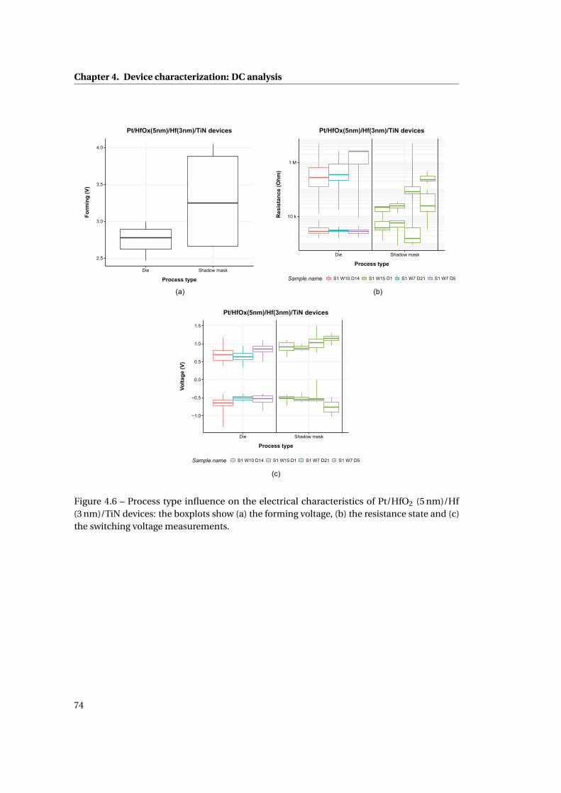
Chapter 4. Device characterization: DC analysis
Figure 4.6 – Process type influence on the electrical characteristics of Pt/HfO2 (5 nm)/Hf(3 nm)/TiN devices: the boxplots show (a) the forming voltage, (b) the resistance state and (c)the switching voltage measurements.
74
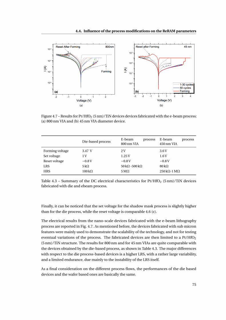
4.4. Influence of the process modifications on the ReRAM parameters
(a) (b)
Figure 4.7 – Results for Pt/HfO2 (5 nm)/TiN devices devices fabricated with the e-beam process:(a) 800 nm VIA and (b) 45 nm VIA diameter device.
Die-based processE-beam process800 nm VIA
E-beam process450 nm VIA
Forming voltage 3.47 V 2 V 3.6 V
Set voltage 1 V 1.25 V 1.6 V
Reset voltage −0.8 V −0.8 V −0.8 V
LRS 5 kΩ 50 kΩ -500 kΩ 80 kΩ
HRS 100 kΩ 5 MΩ 250 kΩ-1 MΩ
Table 4.3 – Summary of the DC electrical characteristics for Pt/HfO2 (5 nm)/TiN devicesfabricated with die and ebeam process.
Finally, it can be noticed that the set voltage for the shadow mask process is slightly higher
than for the die process, while the reset voltage is comparable 4.6 (c).
The electrical results from the nano-scale devices fabricated with the e-beam lithography
process are reported in Fig. 4.7. As mentioned before, the devices fabricated with sub micron
features were mainly used to demonstrate the scalability of the technology, and not for testing
eventual variations of the process. The fabricated devices are then limited to a Pt/HfO2
(5 nm)/TiN structure. The results for 800 nm and for 45 nm VIAs are quite comparable with
the devices obtained by the die-based process, as shown in Table 4.3. The major differences
with respect to the die process-based devices is a higher LRS, with a rather large variability,
and a limited endurance, due mainly to the instability of the LRS itself.
As a final consideration on the different process flows, the performances of the die based
devices and the wafer based ones are basically the same.
75

Chapter 4. Device characterization: DC analysis
4.4.2 Resistive material
The impact of the resistive material type and thickness on the fabricated ReRAMs cells are
reported in Fig. 4.8.
As it is expected, the forming voltage has a clear dependence with respect to the material
used and its thickness. Fig. 4.8 (a) reports the measurement results for several ReRAM devices
with TiN or Pt BE, TiN TE and, when present, Ti 3 nm or Hf 3 nm buffer layers. We decided
to include in the analysis devices with some variation in the cell structure (e.g., considering
different buffer layers) in order to increase the data points for the graph. However, ANOVA
on the forming voltage shows that the resistive material type and thickness is by far the most
important factor for the forming voltage, definitely influencing it more than the BE, TE or an
eventual buffer layer. The graph is then significant even if the device structures are not exactly
the same. The forming voltage increases both for thicker films of the same material, as for the
HfO2 3 nm, 5 nm, 6 nm and 10 nm data points, and for different depositions techniques of the
same material. For example, 10 nm HfO2 deposited by sputtering [HfOx 10 nm (BAS) in the
image] is formless, while the same thickness deposited by ALD (HfOx 10 nm) has a forming
voltage of about 5 V. Also the material type itself influences the forming voltage: 5 min YSZ
and 5 min CGO has similar deposition technique and thicknesses, but quite different forming
values.
The influence on the LRS and HRS is reported in Fig. 4.8 (b). Despite the image has a large
number of information, it is possible to draw two general considerations. First, devices with
thick resistive layers have a smaller resistance window with a larger device-to-device variability.
Examples in the graph are TaOx 25 nm and HfOx 10 nm. This is probably caused by the large
value of the forming voltage, which makes the forming process uncontrollable, resulting into
permanent damages in the resistive oxide film. A second consideration is that devices with
small resistive layer thicknesses, as for HfOx 3 nm, cannot reach very large HRS values, as the
maximum resistance that can be built up in the film is limited by the film thickness.
Similar considerations are valid for the evolution of the set and reset voltage, reported in Fig.
4.8 (c). Thick materials require larger set (positive) and reset (negative) voltages, as the forming
is not optimally controlled, therefore the memories require higher energies to operate. Very
thin materials tend to work at lower operating voltages.
For this work, we decided to mostly focus on 5 nm HfO2. The HfO2 material has been chosen
mainly for the ALD deposition technique, which guarantees good reproducibility and process
control, while the thickness has been optimized with respect to the forming voltage and the
HRS trade-off.
4.4.3 Buffer layer
The buffer layer is a key component in the ReRAM fabrication, and its type and thickness have
a large impact on the cell characteristics. Part of this study has been presented in [65, 66],
76
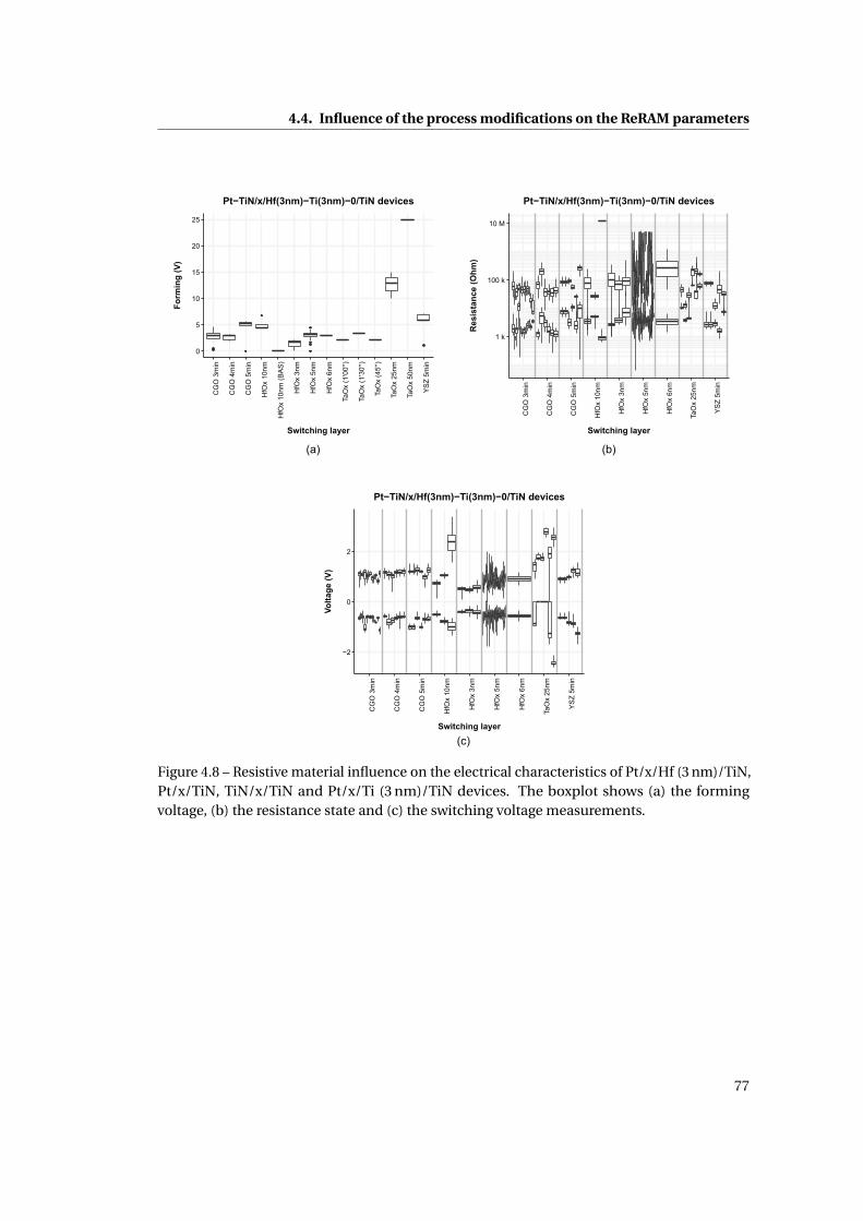
4.4. Influence of the process modifications on the ReRAM parameters
Figure 4.8 – Resistive material influence on the electrical characteristics of Pt/x/Hf (3 nm)/TiN,Pt/x/TiN, TiN/x/TiN and Pt/x/Ti (3 nm)/TiN devices. The boxplot shows (a) the formingvoltage, (b) the resistance state and (c) the switching voltage measurements.
77
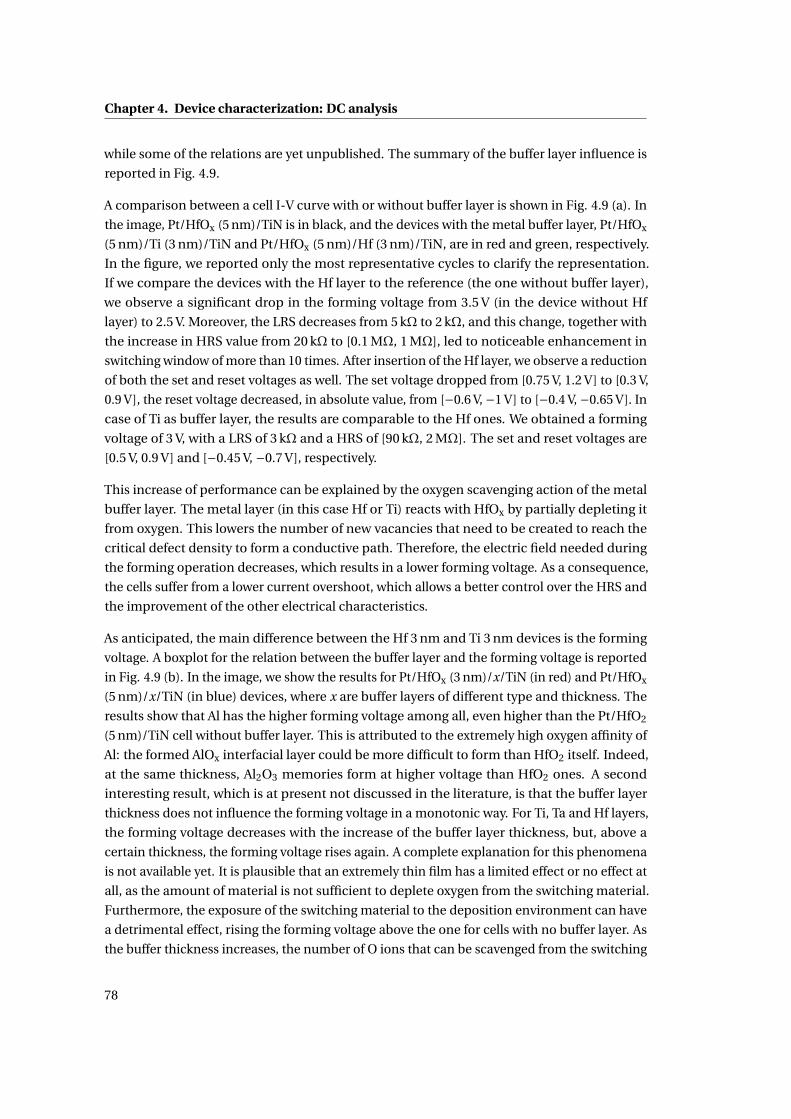
Chapter 4. Device characterization: DC analysis
while some of the relations are yet unpublished. The summary of the buffer layer influence is
reported in Fig. 4.9.
A comparison between a cell I-V curve with or without buffer layer is shown in Fig. 4.9 (a). In
the image, Pt/HfOx (5 nm)/TiN is in black, and the devices with the metal buffer layer, Pt/HfOx
(5 nm)/Ti (3 nm)/TiN and Pt/HfOx (5 nm)/Hf (3 nm)/TiN, are in red and green, respectively.
In the figure, we reported only the most representative cycles to clarify the representation.
If we compare the devices with the Hf layer to the reference (the one without buffer layer),
we observe a significant drop in the forming voltage from 3.5 V (in the device without Hf
layer) to 2.5 V. Moreover, the LRS decreases from 5 kΩ to 2 kΩ, and this change, together with
the increase in HRS value from 20 kΩ to [0.1 MΩ, 1 MΩ], led to noticeable enhancement in
switching window of more than 10 times. After insertion of the Hf layer, we observe a reduction
of both the set and reset voltages as well. The set voltage dropped from [0.75 V, 1.2 V] to [0.3 V,
0.9 V], the reset voltage decreased, in absolute value, from [−0.6 V, −1 V] to [−0.4 V, −0.65 V]. In
case of Ti as buffer layer, the results are comparable to the Hf ones. We obtained a forming
voltage of 3 V, with a LRS of 3 kΩ and a HRS of [90 kΩ, 2 MΩ]. The set and reset voltages are
[0.5 V, 0.9 V] and [−0.45 V, −0.7 V], respectively.
This increase of performance can be explained by the oxygen scavenging action of the metal
buffer layer. The metal layer (in this case Hf or Ti) reacts with HfOx by partially depleting it
from oxygen. This lowers the number of new vacancies that need to be created to reach the
critical defect density to form a conductive path. Therefore, the electric field needed during
the forming operation decreases, which results in a lower forming voltage. As a consequence,
the cells suffer from a lower current overshoot, which allows a better control over the HRS and
the improvement of the other electrical characteristics.
As anticipated, the main difference between the Hf 3 nm and Ti 3 nm devices is the forming
voltage. A boxplot for the relation between the buffer layer and the forming voltage is reported
in Fig. 4.9 (b). In the image, we show the results for Pt/HfOx (3 nm)/x/TiN (in red) and Pt/HfOx
(5 nm)/x/TiN (in blue) devices, where x are buffer layers of different type and thickness. The
results show that Al has the higher forming voltage among all, even higher than the Pt/HfO2
(5 nm)/TiN cell without buffer layer. This is attributed to the extremely high oxygen affinity of
Al: the formed AlOx interfacial layer could be more difficult to form than HfO2 itself. Indeed,
at the same thickness, Al2O3 memories form at higher voltage than HfO2 ones. A second
interesting result, which is at present not discussed in the literature, is that the buffer layer
thickness does not influence the forming voltage in a monotonic way. For Ti, Ta and Hf layers,
the forming voltage decreases with the increase of the buffer layer thickness, but, above a
certain thickness, the forming voltage rises again. A complete explanation for this phenomena
is not available yet. It is plausible that an extremely thin film has a limited effect or no effect at
all, as the amount of material is not sufficient to deplete oxygen from the switching material.
Furthermore, the exposure of the switching material to the deposition environment can have
a detrimental effect, rising the forming voltage above the one for cells with no buffer layer. As
the buffer thickness increases, the number of O ions that can be scavenged from the switching
78
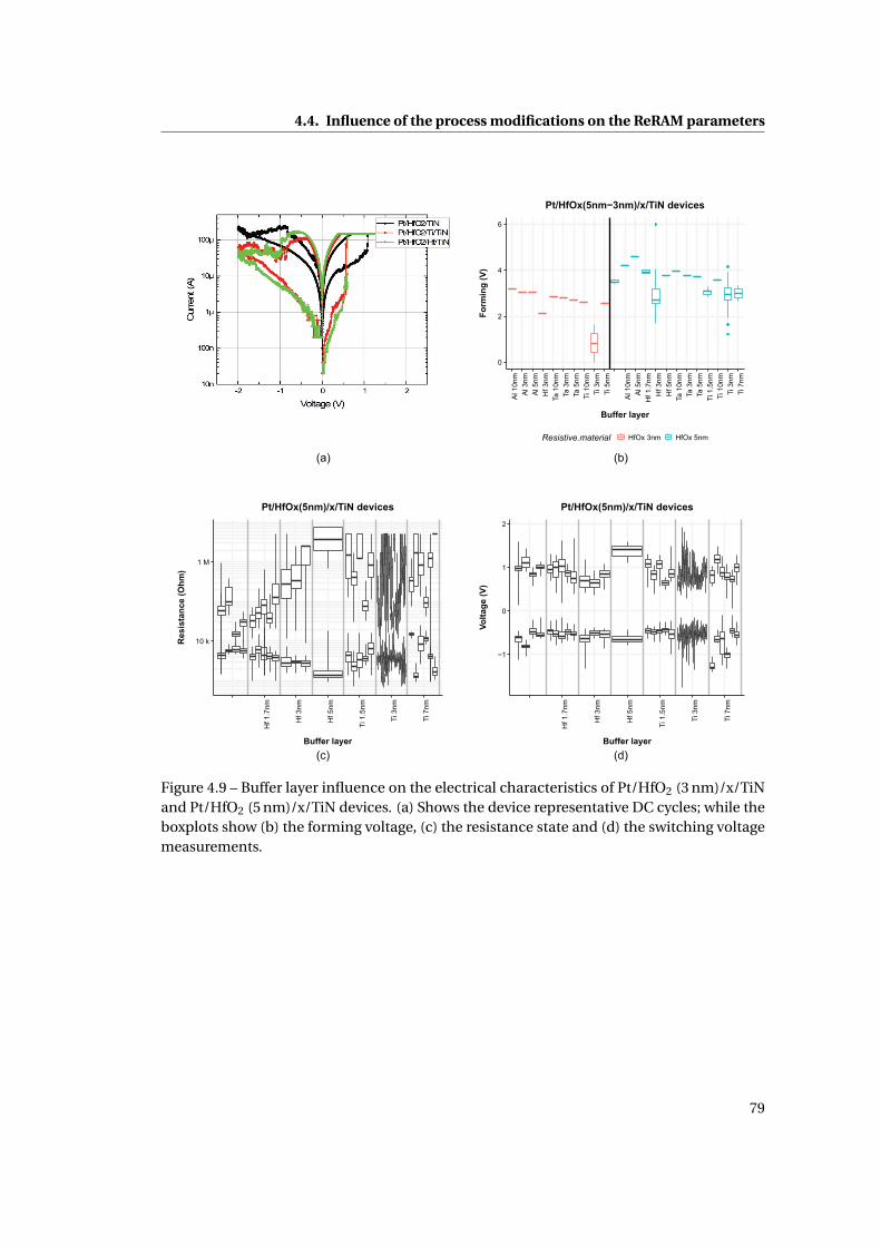
4.4. Influence of the process modifications on the ReRAM parameters
Figure 4.9 – Buffer layer influence on the electrical characteristics of Pt/HfO2 (3 nm)/x/TiNand Pt/HfO2 (5 nm)/x/TiN devices. (a) Shows the device representative DC cycles; while theboxplots show (b) the forming voltage, (c) the resistance state and (d) the switching voltagemeasurements.
79
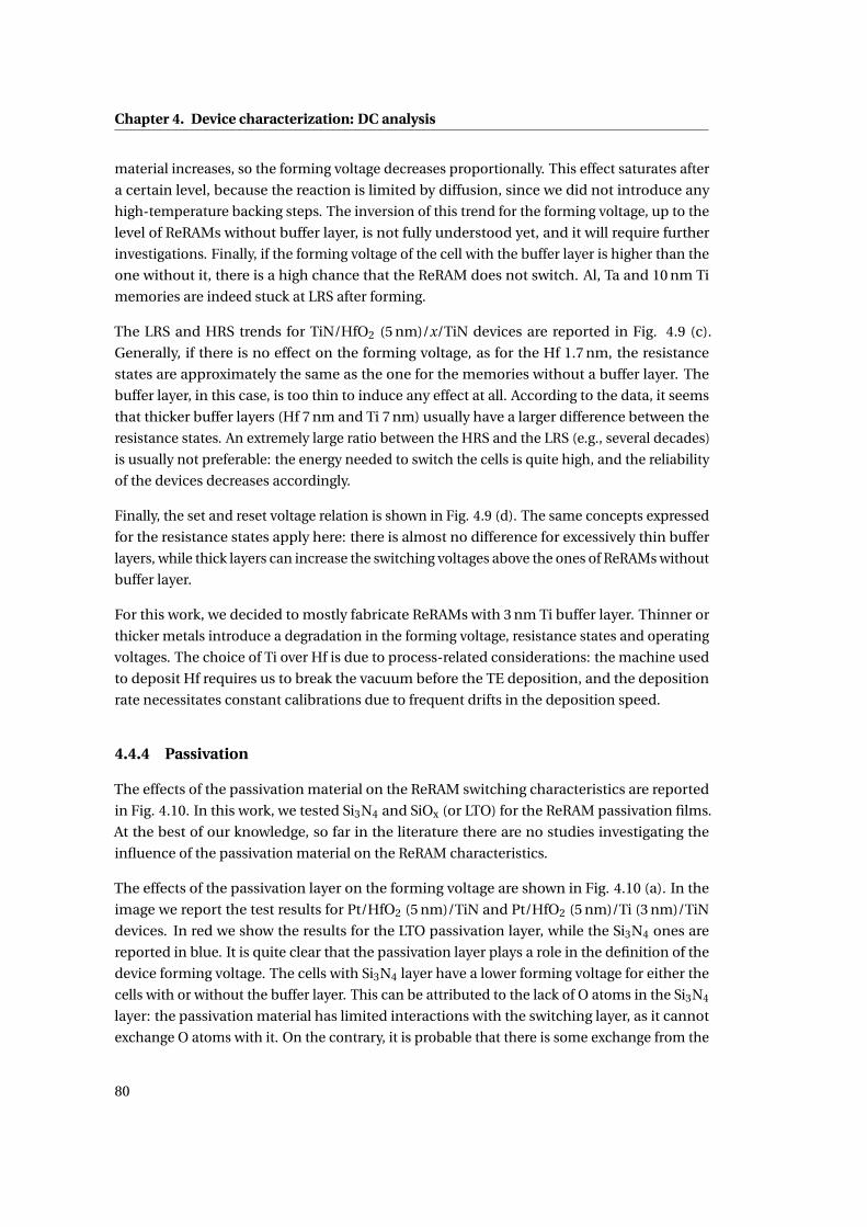
Chapter 4. Device characterization: DC analysis
material increases, so the forming voltage decreases proportionally. This effect saturates after
a certain level, because the reaction is limited by diffusion, since we did not introduce any
high-temperature backing steps. The inversion of this trend for the forming voltage, up to the
level of ReRAMs without buffer layer, is not fully understood yet, and it will require further
investigations. Finally, if the forming voltage of the cell with the buffer layer is higher than the
one without it, there is a high chance that the ReRAM does not switch. Al, Ta and 10 nm Ti
memories are indeed stuck at LRS after forming.
The LRS and HRS trends for TiN/HfO2 (5 nm)/x/TiN devices are reported in Fig. 4.9 (c).
Generally, if there is no effect on the forming voltage, as for the Hf 1.7 nm, the resistance
states are approximately the same as the one for the memories without a buffer layer. The
buffer layer, in this case, is too thin to induce any effect at all. According to the data, it seems
that thicker buffer layers (Hf 7 nm and Ti 7 nm) usually have a larger difference between the
resistance states. An extremely large ratio between the HRS and the LRS (e.g., several decades)
is usually not preferable: the energy needed to switch the cells is quite high, and the reliability
of the devices decreases accordingly.
Finally, the set and reset voltage relation is shown in Fig. 4.9 (d). The same concepts expressed
for the resistance states apply here: there is almost no difference for excessively thin buffer
layers, while thick layers can increase the switching voltages above the ones of ReRAMs without
buffer layer.
For this work, we decided to mostly fabricate ReRAMs with 3 nm Ti buffer layer. Thinner or
thicker metals introduce a degradation in the forming voltage, resistance states and operating
voltages. The choice of Ti over Hf is due to process-related considerations: the machine used
to deposit Hf requires us to break the vacuum before the TE deposition, and the deposition
rate necessitates constant calibrations due to frequent drifts in the deposition speed.
4.4.4 Passivation
The effects of the passivation material on the ReRAM switching characteristics are reported
in Fig. 4.10. In this work, we tested Si3N4 and SiOx (or LTO) for the ReRAM passivation films.
At the best of our knowledge, so far in the literature there are no studies investigating the
influence of the passivation material on the ReRAM characteristics.
The effects of the passivation layer on the forming voltage are shown in Fig. 4.10 (a). In the
image we report the test results for Pt/HfO2 (5 nm)/TiN and Pt/HfO2 (5 nm)/Ti (3 nm)/TiN
devices. In red we show the results for the LTO passivation layer, while the Si3N4 ones are
reported in blue. It is quite clear that the passivation layer plays a role in the definition of the
device forming voltage. The cells with Si3N4 layer have a lower forming voltage for either the
cells with or without the buffer layer. This can be attributed to the lack of O atoms in the Si3N4
layer: the passivation material has limited interactions with the switching layer, as it cannot
exchange O atoms with it. On the contrary, it is probable that there is some exchange from the
80
4.4. Influence of the process modifications on the ReRAM parameters
Figure 4.10 – Passivation influence on the electrical characteristics of Pt/HfO2 (5 nm)/TiN andPt/HfO2 (5 nm)/Ti (3 nm)/TiN devices. The boxplots show (a) the forming voltage, (b) theresistance state and (c) the switching voltage measurements.
81

Chapter 4. Device characterization: DC analysis
LTO to the switching material, and, as a result, the density of vacancies in the switching film
before forming is reduced.
The resistance state characteristics also show a different behavior, as it is shown in Fig. 4.10
(b). The devices with Si3N4 passivation are, in general, more stable across different devices.
In particular, the HRS range shows less fluctuations for both the Ti 3 nm cells and the one
without buffer layer. On the contrary, few memories with LTO passivation report an HRS much
lower than the device average. Again, this can be attributed to the influence of the LTO oxygen
on the switching behavior, which is a destabilizing factor for the ReRAM operation. According
to the location of the switching process, the reset process could indeed be influenced by the
passivation layer. Some of the O ions generated during the set process and out diffusing from
the filament could be trapped in the interface with the passivation layer. This may result in a
limited availability of O atoms for the reset process, which imply in a lower HRS.
Finally, the trend of the passivation layer with respect to the set and reset voltages is shown
in Fig. 4.10 (c). As for the resistance states, the LTO cells show a higher variation in the set
voltages. The two phenomena are most likely related: a higher HRS requires usually a higher
set voltage, as it will be described in Section 4.5.
To summarize, devices with Si3N4 passivation were preferred to the LTO ones because of a
better stability, lower variations and lower operating voltages.
4.4.5 Top electrode etching
In this subsection, we describe the effects of the TE definition on the ReRAM behavior. In the
literature, two studies describes the impact of IBE [67] and RIE [64] on the ReRAM behavior for
cross-point structures. These researches focus mainly on the material sidewall redeposition
and its effect on the memory characteristics. These results are not applicable to our structures,
as the VIA-based structures do not suffer from sidewall redeposition, as the device active area
is embedded in the passivation far away from the etching sidewall. The phenomena described
hereafter are therefore not discussed in the literature.
The effects of etching for the TE definition on the ReRAM behavior is reported in Fig. 4.11.
In the images, we show the patterning of the TE by shadow mask in red (with the label "Not
done"), by RIE in green (with the label "STS", which is the name of the etcher) and by IBE
in blue. The devises considered for this analysis are Pt/HfO2 (5 nm)/TiN, Pt/HfO2 (5 nm)/Hf
(3 nm)/TiN and Pt/HfO2 (5 nm)/Ti (3 nm)/TiN memories.
The effects on the forming voltage are shown in Fig. 4.11 (a). The difference between the
shadow mask and the RIE patterning has been previously described while discussing the
process type effect on the ReRAM characteristics (Subsection 4.4.1). The discrepancy is
attributed to the etching damages related to charge-up effects during the RIE. It is interesting
to notice the difference between the IBE and RIE. The samples with IBE show a lower forming
voltage and, when the number of tested samples becomes large enough, as for the cells with
82
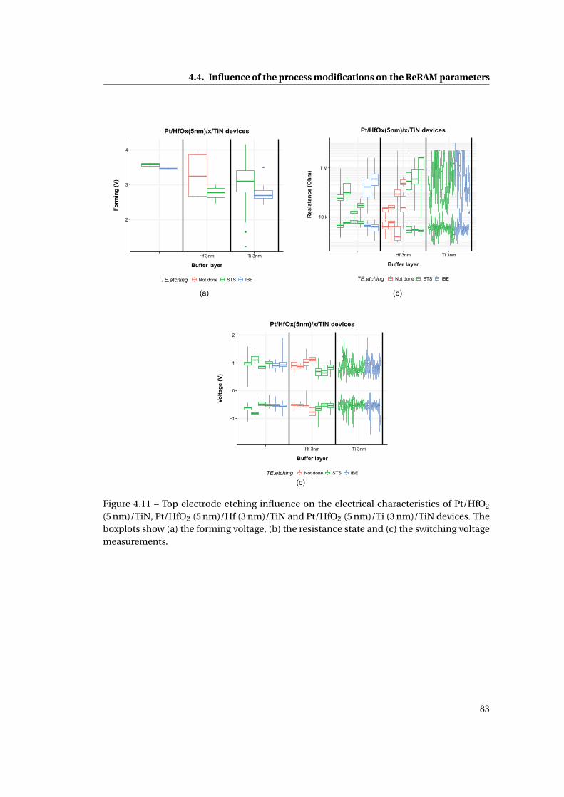
4.4. Influence of the process modifications on the ReRAM parameters
Figure 4.11 – Top electrode etching influence on the electrical characteristics of Pt/HfO2
(5 nm)/TiN, Pt/HfO2 (5 nm)/Hf (3 nm)/TiN and Pt/HfO2 (5 nm)/Ti (3 nm)/TiN devices. Theboxplots show (a) the forming voltage, (b) the resistance state and (c) the switching voltagemeasurements.
83
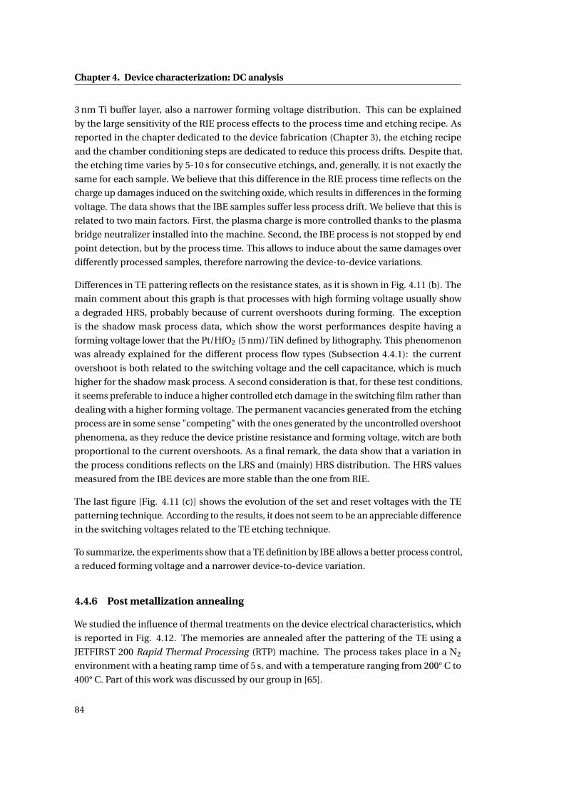
Chapter 4. Device characterization: DC analysis
3 nm Ti buffer layer, also a narrower forming voltage distribution. This can be explained
by the large sensitivity of the RIE process effects to the process time and etching recipe. As
reported in the chapter dedicated to the device fabrication (Chapter 3), the etching recipe
and the chamber conditioning steps are dedicated to reduce this process drifts. Despite that,
the etching time varies by 5-10 s for consecutive etchings, and, generally, it is not exactly the
same for each sample. We believe that this difference in the RIE process time reflects on the
charge up damages induced on the switching oxide, which results in differences in the forming
voltage. The data shows that the IBE samples suffer less process drift. We believe that this is
related to two main factors. First, the plasma charge is more controlled thanks to the plasma
bridge neutralizer installed into the machine. Second, the IBE process is not stopped by end
point detection, but by the process time. This allows to induce about the same damages over
differently processed samples, therefore narrowing the device-to-device variations.
Differences in TE pattering reflects on the resistance states, as it is shown in Fig. 4.11 (b). The
main comment about this graph is that processes with high forming voltage usually show
a degraded HRS, probably because of current overshoots during forming. The exception
is the shadow mask process data, which show the worst performances despite having a
forming voltage lower that the Pt/HfO2 (5 nm)/TiN defined by lithography. This phenomenon
was already explained for the different process flow types (Subsection 4.4.1): the current
overshoot is both related to the switching voltage and the cell capacitance, which is much
higher for the shadow mask process. A second consideration is that, for these test conditions,
it seems preferable to induce a higher controlled etch damage in the switching film rather than
dealing with a higher forming voltage. The permanent vacancies generated from the etching
process are in some sense "competing" with the ones generated by the uncontrolled overshoot
phenomena, as they reduce the device pristine resistance and forming voltage, witch are both
proportional to the current overshoots. As a final remark, the data show that a variation in
the process conditions reflects on the LRS and (mainly) HRS distribution. The HRS values
measured from the IBE devices are more stable than the one from RIE.
The last figure [Fig. 4.11 (c)] shows the evolution of the set and reset voltages with the TE
patterning technique. According to the results, it does not seem to be an appreciable difference
in the switching voltages related to the TE etching technique.
To summarize, the experiments show that a TE definition by IBE allows a better process control,
a reduced forming voltage and a narrower device-to-device variation.
4.4.6 Post metallization annealing
We studied the influence of thermal treatments on the device electrical characteristics, which
is reported in Fig. 4.12. The memories are annealed after the pattering of the TE using a
JETFIRST 200 Rapid Thermal Processing (RTP) machine. The process takes place in a N2
environment with a heating ramp time of 5 s, and with a temperature ranging from 200° C to
400° C. Part of this work was discussed by our group in [65].
84
4.4. Influence of the process modifications on the ReRAM parameters
Figure 4.12 – Annealing influence on the electrical characteristics of Pt/HfO2 (5 nm)/Hf(3 nm)/TiN devices. (a) Shows the device representative DC cycles; while the boxplots show(b) the forming voltage, (c) the resistance state and (d) the switching voltage measurements.
85
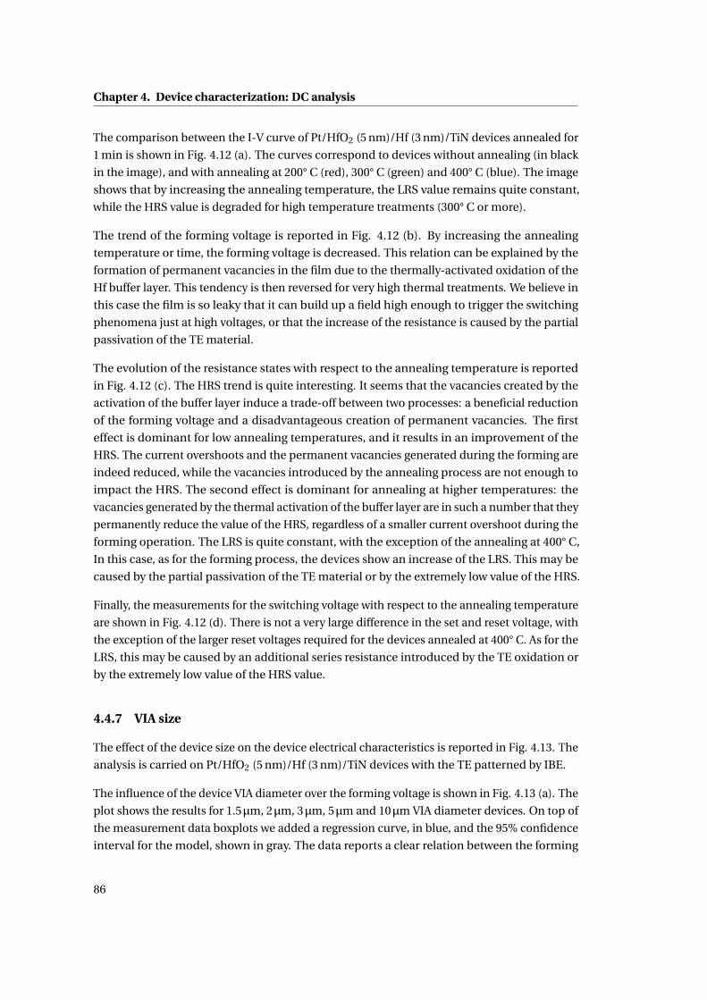
Chapter 4. Device characterization: DC analysis
The comparison between the I-V curve of Pt/HfO2 (5 nm)/Hf (3 nm)/TiN devices annealed for
1 min is shown in Fig. 4.12 (a). The curves correspond to devices without annealing (in black
in the image), and with annealing at 200° C (red), 300° C (green) and 400° C (blue). The image
shows that by increasing the annealing temperature, the LRS value remains quite constant,
while the HRS value is degraded for high temperature treatments (300° C or more).
The trend of the forming voltage is reported in Fig. 4.12 (b). By increasing the annealing
temperature or time, the forming voltage is decreased. This relation can be explained by the
formation of permanent vacancies in the film due to the thermally-activated oxidation of the
Hf buffer layer. This tendency is then reversed for very high thermal treatments. We believe in
this case the film is so leaky that it can build up a field high enough to trigger the switching
phenomena just at high voltages, or that the increase of the resistance is caused by the partial
passivation of the TE material.
The evolution of the resistance states with respect to the annealing temperature is reported
in Fig. 4.12 (c). The HRS trend is quite interesting. It seems that the vacancies created by the
activation of the buffer layer induce a trade-off between two processes: a beneficial reduction
of the forming voltage and a disadvantageous creation of permanent vacancies. The first
effect is dominant for low annealing temperatures, and it results in an improvement of the
HRS. The current overshoots and the permanent vacancies generated during the forming are
indeed reduced, while the vacancies introduced by the annealing process are not enough to
impact the HRS. The second effect is dominant for annealing at higher temperatures: the
vacancies generated by the thermal activation of the buffer layer are in such a number that they
permanently reduce the value of the HRS, regardless of a smaller current overshoot during the
forming operation. The LRS is quite constant, with the exception of the annealing at 400° C,
In this case, as for the forming process, the devices show an increase of the LRS. This may be
caused by the partial passivation of the TE material or by the extremely low value of the HRS.
Finally, the measurements for the switching voltage with respect to the annealing temperature
are shown in Fig. 4.12 (d). There is not a very large difference in the set and reset voltage, with
the exception of the larger reset voltages required for the devices annealed at 400° C. As for the
LRS, this may be caused by an additional series resistance introduced by the TE oxidation or
by the extremely low value of the HRS value.
4.4.7 VIA size
The effect of the device size on the device electrical characteristics is reported in Fig. 4.13. The
analysis is carried on Pt/HfO2 (5 nm)/Hf (3 nm)/TiN devices with the TE patterned by IBE.
The influence of the device VIA diameter over the forming voltage is shown in Fig. 4.13 (a). The
plot shows the results for 1.5μm, 2μm, 3μm, 5μm and 10μm VIA diameter devices. On top of
the measurement data boxplots we added a regression curve, in blue, and the 95% confidence
interval for the model, shown in gray. The data reports a clear relation between the forming
86
4.4. Influence of the process modifications on the ReRAM parameters
R2 0.774
2.98
0.22
Figure 4.13 – VIA size influence on the electrical characteristics of Pt/HfO2 (5 nm)/Hf(3 nm)/TiN devices with IBE TE etching. The boxplots show (a) the forming voltage, (b)the resistance state and (c) the switching voltage measurements.
87
Chapter 4. Device characterization: DC analysis
voltage and the device size: as the device area increases, the forming voltage decreases. This
dependance has been described by a first order analytical model based on percolation theory
by Chen [68]. As described in the introduction (Section 2.3), the forming process triggers when
there is a path from the TE to the BE with a sufficiently high density of oxygen vacancies. This
problem can be described by the percolation theory, a branch of statistics that describes the
behavior of connected clusters. Intuitively, it can be understood that the smaller the device
area, the less the probability that exists vacancy clusters which are close enough to trigger the
forming process. This is a statistical characteristics which is independent of specific materials
thicknesses and defect densities. The dependence between the forming voltage and the device
area can be simplified by Equation 4.1:
Vf =α+β ln
(A
a2
)(4.1)
where Vf is the forming voltage, A the device area and a2 the size of the side of the small cubic
cells in which the switching volume is divided into in order to carry on the analysis (more
details in [68]). We fit our data with the expression reported in Equation 4.1, and the result of
the regression is plotted in blue on top of the data measurements. We obtained a value for α
of 2.98 and β value of −0.22, with a model R2 of 0.774. This first order analytical model seems
to be consistent with our results.
The resistance state and the switching voltage variations with respect to the device area are
shown in Fig. 4.13 (b) and Fig. 4.13 (c), respectively. At this device sizes, the data do not show
any clear dependence with the VIA diameter.
4.4.8 Bottom electrode, top electrode and capping layer
In this work, we fabricated devices with TiN and Pt BE. We were aiming at replacing the Pt BE
in Pt/HfO2 (5 nm)/Ti (3 nm)/TiN with TiN, in order to make it easier to integrate the ReRAM
cells into a CMOS process. Unfortunately, the attempts were unsatisfactory, and further
optimizations are required. Even if the forming voltage of the Pt/HfO2 (5 nm)/Ti (3 nm)/TiN
and TiN/HfO2 (5 nm)/Ti (3 nm)/TiN cells is the same, the latter devices were quite difficult to
test. The cells show a reverse breakdown at −1 V, i.e., when the reset voltage exceeds this value,
the polarity of the cell changes and the memory goes into a LRS. The reverse breakdown value
for the ReRAMs with Pt BE is between −2.5 V and −3 V. Limiting the reset voltage at small values
allowed to cycle the TiN cells, with the drawback of an extremely limited resistance window.
Treatments of the BE surface with SC1 solution couldn’t mitigate this problem, and slightly
increased the forming voltage. We believe that the problem is the excessive device symmetry.
The low reverse breakdown voltage can be attributed to the reaction of the TiN BE with the
O atoms ejected from the oxide material lattice, once the field reaches a certain threshold.
Furthermore, an additional factor may be the difference in the device band structure due to the
88
4.5. Correlation between the ReRAM characteristics
presence of TiN or Pt on the BE. Indeed, at a defined applied voltage, due to the band structure
the tunnel distance is smaller for the TiN BE than for Pt one. This may allow, while the cell is
in the HRS, a sudden increase of the current flow through the cell while it reaches the reverse
breakdown voltage. A reverse field coupled with a relatively high current could then induce a
reverse set, changing the resistance state to the LRS. Possible solutions to this phenomena
could be using a thicker buffer layer and introducing a post metallization annealing step, in
order to try to make the memory properties more asymmetric, or to insert a barrier above the
BE.
We tested three type of TE on Pt/HfO2 (5 nm)/x devices: the standard TiN, TiN deposited by
reactive sputtering and W. Both W and the reactively sputtered TiN devices showed very large
currents for the first reset (usually about 10 mA). It is quite interesting to compare the two TiN
films deposited by different techniques (normal or reactive sputtering). Despite the measured
forming voltages are the same, the reactive-sputtered TiN shows large current overshoots
during the forming operation, which result on a small resistance window (about 5) and a large
voltage required for the first reset (between −2 V and −3 V). At present, we do not have an
explanation for this phenomena, especially considering the TiN resistivity is lower for the
reactive-sputtered films.
Finally, we discuss the capping of the electrode pad for the fabricated cells. We tested Pt/HfO2
(5 nm)/Ti (3 nm)/TiN with and without an Al capping layer covering the TE. The test shows that
the forming voltage is slightly reduced for the cells with the Al layer, but the overall switching
performances are slightly degraded. The resistance window is reduced, especially because
of a low HRS. The decrease of the switching voltage could be explained by the effect of the
Al barrier against the TiN oxidation, while the performance degradation is not yet clearly
understood. A possible cause could be the longer RIE TE etch, needed to pattern both the TiN
and the Al, but further experiments should be performed in order to validate this theory.
4.5 Correlation between the ReRAM characteristics
In this section, we discuss the relation between the ReRAM electrical characteristics measured
during the DC tests. In the previous section (Section 4.4) we described how the process
modifications (the test inputs) relates with the ReRAM electrical parameters (the test outputs).
The aim is now to show how the outputs are intercorrelated for a large selection of memory
cells that differ in materials, size and fabrication steps. This study target to demonstrate the
validity of the characterization methodology and the intrinsic relations between the ReRAM
key switching parameters. For the second goal, it is important to highlight the aim is to
investigate the bipolar OxRAM category in general, beyond a specific device material or size.
This is particularly relevant as the described relations may have a universal value, since they
are obtained from a varied population of memory devices.
Recently a comparable study on unipolar devices by modifying the test conditions (e.g., the
current compliance) has been reported in [69], however, it mainly focused on the relation
89
Chapter 4. Device characterization: DC analysis
between switching power and resistance. Regarding bipolar OxRAM devices, the relation
between two of these factors for a single device type is presented in [70, 71]. So far in the
literature, a systematic study covering all these factors with a large variation in materials and
fabrication procedure has not been reported. This analysis has been submitted for publication
in [72].
In order to simplify the dissertation, the text is divided into subsections based on the number
of observable considered in the analysis. First, Subsection 4.5.1 shows the relation between
the forming, set and reset voltages. Then, Subsection 4.5.2 reports on the relation between the
forming, set and reset voltages with the resistance states. Finally, Subsection 4.5.3 discuss the
correlation between all the measured characteristics.
4.5.1 Forming, set and reset voltage relation
The relation between the forming voltage, the median set voltage and the median reset voltage
is reported in Fig. 4.14 and Fig. 4.15 for all the ReRAM cells and the cells based on HfO2 (5 nm),
respectively. The figures are composed by nine elements each. The diagonal elements show
the density plots obtained from the data distribution. For example, the data reports that a high
number of ReRAM cells that have a forming voltage around 3 V (Fig. 4.14, top left graph). The
numbers in the graph elements above the diagonal are the calculated Pearson’s correlation
coefficients. The correlation number refers to the two quantities reported on the x- and y-axis.
For example, in case of the HfO2 (5 nm) devices, the correlation between the forming voltage
and the set voltage is 0.354 (Fig. 4.15, top row, middle column). The remaining plots below the
diagonal elements are the scatterplots of the measured quantities. The x-axis is common for
all the plots on the same column, while the y-axis is in common for all the plots in the same
row. For instance, the middle plot in the bottom row shows the datapoints for the set voltage
(x-axis) and the reset voltage (y-axis). Above the datapoints we added the linear regression
of the data, in blue, and the local polynomial regression fitting line, in red. The color band
indicates the 95% confidence level interval of predictions for the two models.
Before proceeding with the discussion of the results, we should make two general considera-
tions about the calculated correlation coefficients and the data points.
First, it should be noted that the coefficients may be quite different according to the considered
group of devices. Even if the HfO2 (5 nm) ReRAM is a subgroup of the whole fabricated ReRAM
devices, the analysis on such a group leads to different results. The reason lies mainly in
the quality of the data available. As the device fabrication was tailored to the optimization
of the ReRAM performances, the data tends to be clustered around some optimal values.
This results in a strongly uneven distribution of the datapoints, especially for the plots that
consider all the fabricated devices. This is evident from the density plots, which are more
sharp for the global ReRAM devices (Fig. 4.14) with respect to the HfO2 (5 nm) based ones
(Fig. 4.15). As a consequence, for the ReRAM devices reported in the Fig. Fig. 4.14, few points
at the extremes of the domain can have a very high leverage in the analysis, resulting in very
90
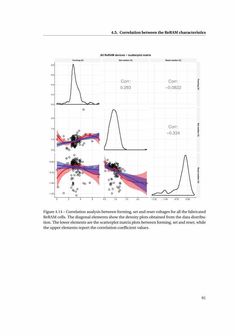
4.5. Correlation between the ReRAM characteristics
Corr:0.283
Corr:
Corr:
Figure 4.14 – Correlation analysis between forming, set and reset voltages for all the fabricatedReRAM cells. The diagonal elements show the density plots obtained from the data distribu-tion. The lower elements are the scatterplot matrix plots between forming, set and reset, whilethe upper elements report the correlation coefficient values.
91
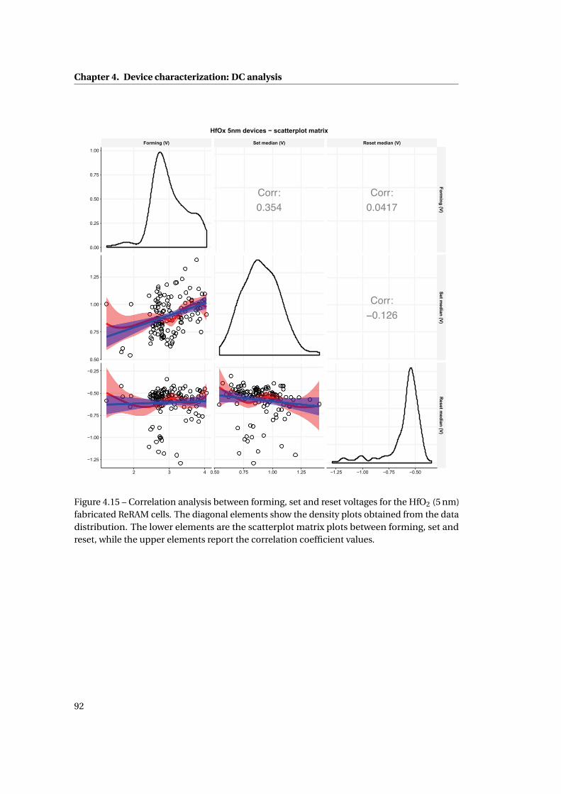
Chapter 4. Device characterization: DC analysis
Corr:0.354
Corr:0.0417
Corr:
Figure 4.15 – Correlation analysis between forming, set and reset voltages for the HfO2 (5 nm)fabricated ReRAM cells. The diagonal elements show the density plots obtained from the datadistribution. The lower elements are the scatterplot matrix plots between forming, set andreset, while the upper elements report the correlation coefficient values.
92
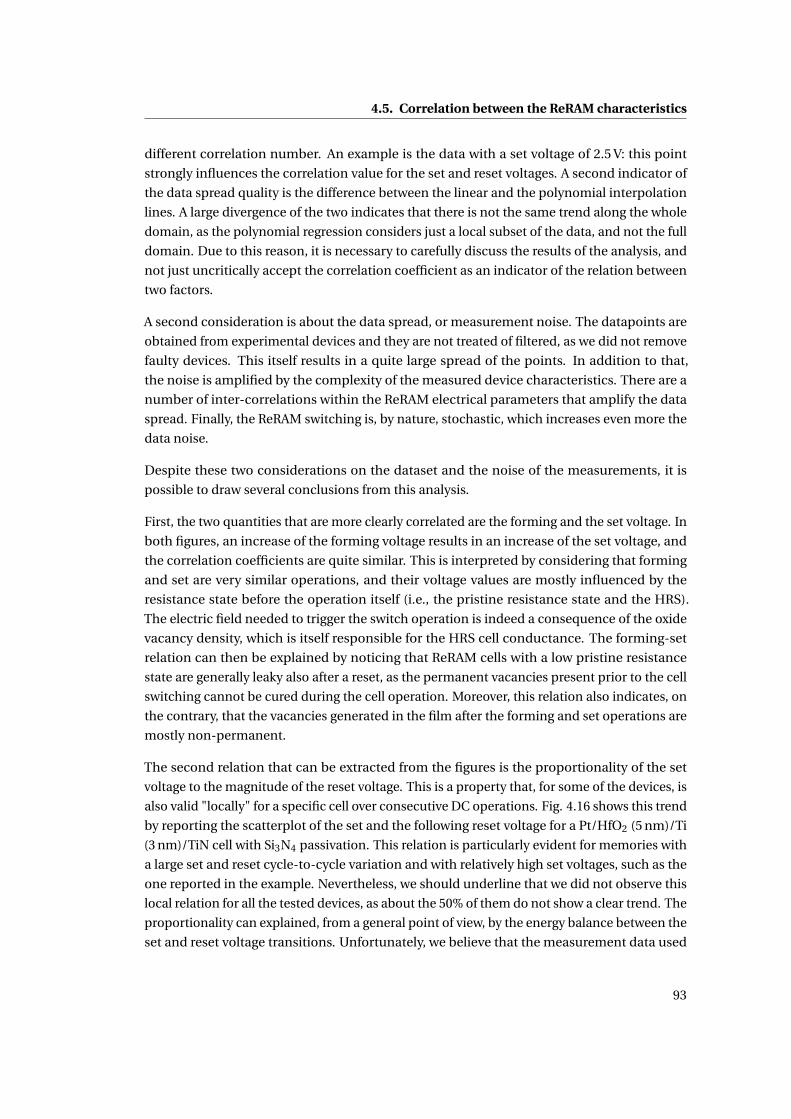
4.5. Correlation between the ReRAM characteristics
different correlation number. An example is the data with a set voltage of 2.5 V: this point
strongly influences the correlation value for the set and reset voltages. A second indicator of
the data spread quality is the difference between the linear and the polynomial interpolation
lines. A large divergence of the two indicates that there is not the same trend along the whole
domain, as the polynomial regression considers just a local subset of the data, and not the full
domain. Due to this reason, it is necessary to carefully discuss the results of the analysis, and
not just uncritically accept the correlation coefficient as an indicator of the relation between
two factors.
A second consideration is about the data spread, or measurement noise. The datapoints are
obtained from experimental devices and they are not treated of filtered, as we did not remove
faulty devices. This itself results in a quite large spread of the points. In addition to that,
the noise is amplified by the complexity of the measured device characteristics. There are a
number of inter-correlations within the ReRAM electrical parameters that amplify the data
spread. Finally, the ReRAM switching is, by nature, stochastic, which increases even more the
data noise.
Despite these two considerations on the dataset and the noise of the measurements, it is
possible to draw several conclusions from this analysis.
First, the two quantities that are more clearly correlated are the forming and the set voltage. In
both figures, an increase of the forming voltage results in an increase of the set voltage, and
the correlation coefficients are quite similar. This is interpreted by considering that forming
and set are very similar operations, and their voltage values are mostly influenced by the
resistance state before the operation itself (i.e., the pristine resistance state and the HRS).
The electric field needed to trigger the switch operation is indeed a consequence of the oxide
vacancy density, which is itself responsible for the HRS cell conductance. The forming-set
relation can then be explained by noticing that ReRAM cells with a low pristine resistance
state are generally leaky also after a reset, as the permanent vacancies present prior to the cell
switching cannot be cured during the cell operation. Moreover, this relation also indicates, on
the contrary, that the vacancies generated in the film after the forming and set operations are
mostly non-permanent.
The second relation that can be extracted from the figures is the proportionality of the set
voltage to the magnitude of the reset voltage. This is a property that, for some of the devices, is
also valid "locally" for a specific cell over consecutive DC operations. Fig. 4.16 shows this trend
by reporting the scatterplot of the set and the following reset voltage for a Pt/HfO2 (5 nm)/Ti
(3 nm)/TiN cell with Si3N4 passivation. This relation is particularly evident for memories with
a large set and reset cycle-to-cycle variation and with relatively high set voltages, such as the
one reported in the example. Nevertheless, we should underline that we did not observe this
local relation for all the tested devices, as about the 50% of them do not show a clear trend. The
proportionality can explained, from a general point of view, by the energy balance between the
set and reset voltage transitions. Unfortunately, we believe that the measurement data used
93
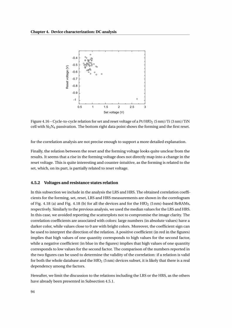
Chapter 4. Device characterization: DC analysis
Figure 4.16 – Cycle-to-cycle relation for set and reset voltage of a Pt/HfO2 (5 nm)/Ti (3 nm)/TiNcell with Si3N4 passivation. The bottom right data point shows the forming and the first reset.
for the correlation analysis are not precise enough to support a more detailed explanation.
Finally, the relation between the reset and the forming voltage looks quite unclear from the
results. It seems that a rise in the forming voltage does not directly map into a change in the
reset voltage. This is quite interesting and counter-intuitive, as the forming is related to the
set, which, on its part, is partially related to reset voltage.
4.5.2 Voltages and resistance states relation
In this subsection we include in the analysis the LRS and HRS. The obtained correlation coeffi-
cients for the forming, set, reset, LRS and HRS measurements are shown in the correlogram
of Fig. 4.18 (a) and Fig. 4.18 (b) for all the devices and for the HfO2 (5 nm)-based ReRAMs,
respectively. Similarly to the previous analysis, we used the median values for the LRS and HRS.
In this case, we avoided reporting the scatterplots not to compromise the image clarity. The
correlation coefficients are associated with colors: large numbers (in absolute values) have a
darker color, while values close to 0 are with bright colors. Moreover, the coefficient sign can
be used to interpret the direction of the relation. A positive coefficient (in red in the figures)
implies that high values of one quantity corresponds to high values for the second factor,
while a negative coefficient (in blue in the figures) implies that high values of one quantity
corresponds to low values for the second factor. The comparison of the numbers reported in
the two figures can be used to determine the validity of the correlation: if a relation is valid
for both the whole database and the HfO2 (5 nm) devices subset, it is likely that there is a real
dependency among the factors.
Hereafter, we limit the discussion to the relations including the LRS or the HRS, as the others
have already been presented in Subsection 4.5.1.
94
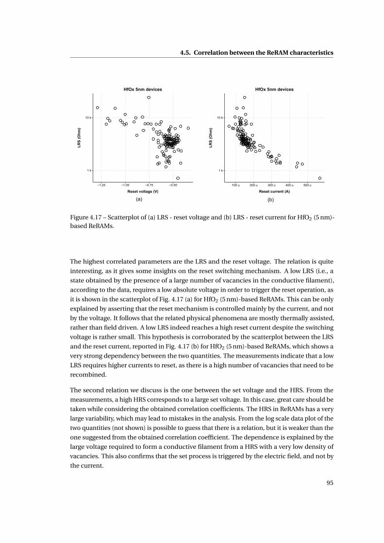
4.5. Correlation between the ReRAM characteristics
Figure 4.17 – Scatterplot of (a) LRS - reset voltage and (b) LRS - reset current for HfO2 (5 nm)-based ReRAMs.
The highest correlated parameters are the LRS and the reset voltage. The relation is quite
interesting, as it gives some insights on the reset switching mechanism. A low LRS (i.e., a
state obtained by the presence of a large number of vacancies in the conductive filament),
according to the data, requires a low absolute voltage in order to trigger the reset operation, as
it is shown in the scatterplot of Fig. 4.17 (a) for HfO2 (5 nm)-based ReRAMs. This can be only
explained by asserting that the reset mechanism is controlled mainly by the current, and not
by the voltage. It follows that the related physical phenomena are mostly thermally assisted,
rather than field driven. A low LRS indeed reaches a high reset current despite the switching
voltage is rather small. This hypothesis is corroborated by the scatterplot between the LRS
and the reset current, reported in Fig. 4.17 (b) for HfO2 (5 nm)-based ReRAMs, which shows a
very strong dependency between the two quantities. The measurements indicate that a low
LRS requires higher currents to reset, as there is a high number of vacancies that need to be
recombined.
The second relation we discuss is the one between the set voltage and the HRS. From the
measurements, a high HRS corresponds to a large set voltage. In this case, great care should be
taken while considering the obtained correlation coefficients. The HRS in ReRAMs has a very
large variability, which may lead to mistakes in the analysis. From the log scale data plot of the
two quantities (not shown) is possible to guess that there is a relation, but it is weaker than the
one suggested from the obtained correlation coefficient. The dependence is explained by the
large voltage required to form a conductive filament from a HRS with a very low density of
vacancies. This also confirms that the set process is triggered by the electric field, and not by
the current.
95
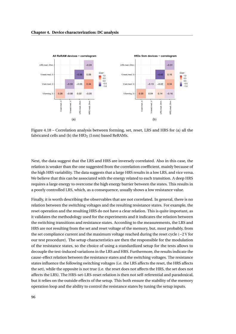
Chapter 4. Device characterization: DC analysis
0.35 0.04 0.14
0.340.44
Figure 4.18 – Correlation analysis between forming, set, reset, LRS and HRS for (a) all thefabricated cells and (b) the HfO2 (5 nm) based ReRAMs.
Next, the data suggest that the LRS and HRS are inversely correlated. Also in this case, the
relation is weaker than the one suggested from the correlation coefficient, mainly because of
the high HRS variability. The data suggests that a large HRS results in a low LRS, and vice versa.
We believe that this can be associated with the energy related to each transition. A deep HRS
requires a large energy to overcome the high energy barrier between the states. This results in
a poorly controlled LRS, which, as a consequence, usually shows a low resistance value.
Finally, it is worth describing the observables that are not correlated. In general, there is no
relation between the switching voltages and the resulting resistance states. For example, the
reset operation and the resulting HRS do not have a clear relation. This is quite important, as
it validates the methodology used for the experiments and it indicates the relation between
the switching transitions and resistance states. According to the measurements, the LRS and
HRS are not resulting from the set and reset voltage of the memory, but, most probably, from
the set compliance current and the maximum voltage reached during the reset cycle (−2 V for
our test procedure). The setup characteristics are then the responsible for the modulation
of the resistance states, so the choice of using a standardized setup for the tests allows to
decouple the test-induced variations in the LRS and HRS. Furthermore, the results indicate the
cause-effect relation between the resistance states and the switching voltages. The resistance
states influence the following switching voltages (i.e. the LRS affects the reset, the HRS affects
the set), while the opposite is not true (i.e. the reset does not affects the HRS, the set does not
affects the LRS). The HRS-set-LRS-reset relation is then not self-referential and paradoxical,
but it relies on the outside effects of the setup. This both ensure the stability of the memory
operation loop and the ability to control the resistance states by tuning the setup inputs.
96
4.6. Retention tests
4.5.3 All switching parameters relation
To conclude the correlation analysis, we report in Fig. 4.19 and Fig. 4.20 the full correlogram
that includes all the observables for the whole database and for the HfO2 (5 nm) subset,
respectively. The additional observables are the forming current, the first reset voltage and
current, the log value for the LRS and HRS, the set and reset currents, and the set and reset
power. This last item is calculated by multiplying the voltage and the current fro the set and
reset.
Because of the high number of information, we did not report the data correlogram, and
hereafter we just limit the discussion to the main features.
From the analysis, one of the most interesting relation is the one describing the current
overshoot. As reported before, the current reached during the first reset is believed to be about
the same as the one reached during the forming current overshoot. Current overshoots are
intrinsic to ReRAM nature, as they are generated by the positive feedback between the vacancy
generation and the current increase during the set and forming operation. This sudden rise of
the device current needs to be limited externally. As reported in Section 4.3, from an electrical
point of view, the overshoot effects resulting from the forming and set operation is related
to the capacitance in series to the cell electrodes, the transition voltage and the difference
between the starting and the final value of the current transient. The measurements confirm
these dependencies, as the first reset current is highly correlated to the forming voltage (r is
0.33 and 0.42 for all the devices and the HfO2 (5 nm) ones, respectively). Moreover, it should
be highlighted that the first reset current is weakly correlated with the LRS (r is 0.17 and
0.16 for the two datasets). This suggests that the forming overshoot effect, for our setup
and for the type of memories that we fabricated, does not have a large influence on the cell
characteristics. This is especially valid for the HfO2 (5 nm) memories, which, because of lower
forming voltages, shows a minor dependency between the first reset current and the other
parameters.
Finally, it should be noted that the set and reset power are highly correlated (r is −0.52 for the
whole database). This is in accordance with the hypothesis that the memory cell tends to find
an energy balance for resistance states, as reported in Subsection 4.5.2 and Subsection 4.5.1.
4.6 Retention tests
We performed data retention tests for the Pt/HfO2 (5 nm)/TiN devices. The setup is similar to
the one used for the DC tests, with the difference that we used a motorized probe station, a
thermal chuck and a different parameter analyzer (with slightly different settings). The whole
system is run by a custom Matlab program, which controls the different instruments via GPIB.
First, the tests are carried on 19 devices on the same wafer at room temperature. The results
for the HRS and LRS are reported in Fig. 4.21 (a) and Fig. 4.21 (b), respectively. The memories
97

Chapter 4. Device characterization: DC analysis
Figure 4.19 – Correlation analysis between all the measured electrical characteristics for all thefabricated ReRAM cells.
98
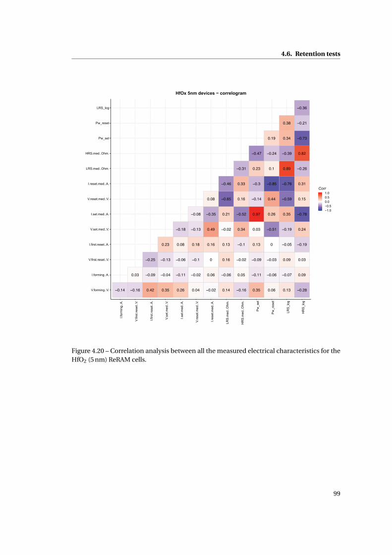
4.6. Retention tests
Figure 4.20 – Correlation analysis between all the measured electrical characteristics for theHfO2 (5 nm) ReRAM cells.
99
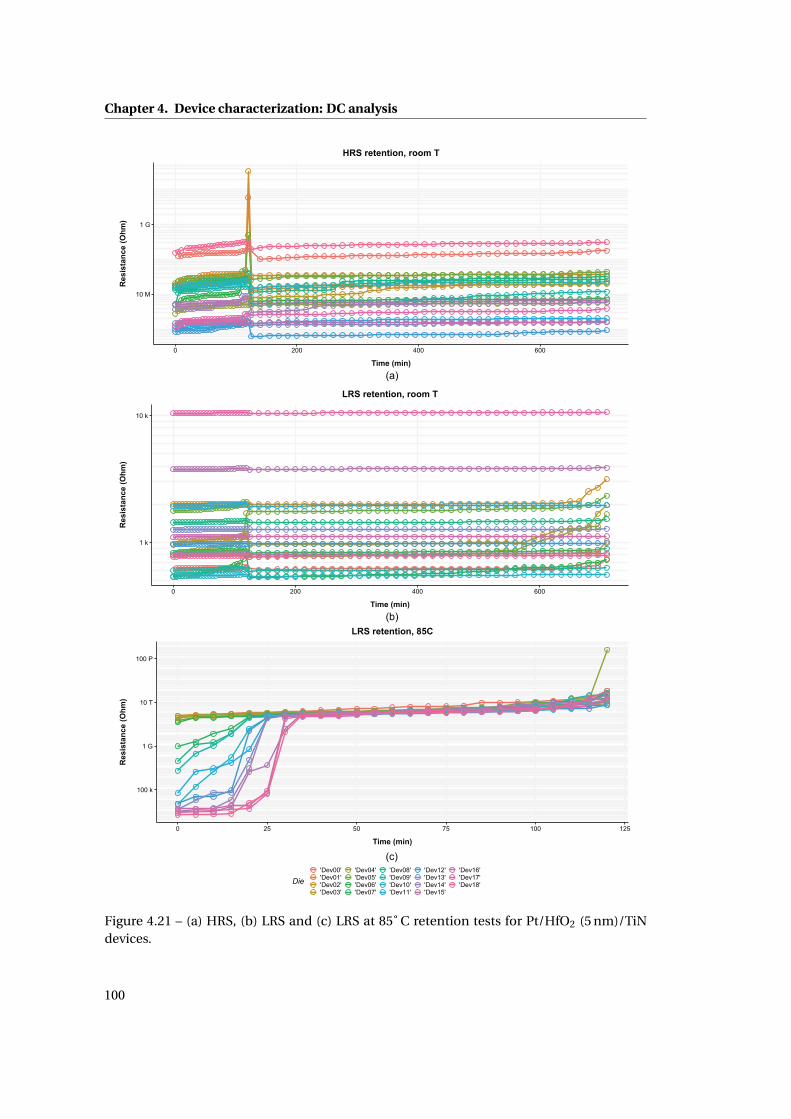
Chapter 4. Device characterization: DC analysis
Figure 4.21 – (a) HRS, (b) LRS and (c) LRS at 85˚ C retention tests for Pt/HfO2 (5 nm)/TiNdevices.
100
4.7. Summary
are formed and then cycled for 50 cycles. For the first experiment, the devices were left in HRS
after resetting at -2.5 V. Then, a read operation was performed sequentially on each cell for
the next 11 hours. All devices tested exhibited good data retention characteristics under room
temperature conditions as shown in Fig. 4.21 (a). The difference in the data sampling at the
120 min mark and the measured resistance spike is caused by the launch of a new test. The
next day, the devices were set and left in the LRS. Again, a read was performed for the next
11 hours. The data retention was confirmed, as shown in Fig. 4.21 (b). As for the HRS, the
difference in the data sampling at about 120 min is related to the launch of a new test.
The same experiment was then performed at 85° C as shown in Fig. 4.21 (c). In this case,
each of the devices was set to LRS after being cycled for 50 times at 85° C. As the DC cycling
operation is sequential, the time elapsed to cycle and set the devices to the LRS between the
first and last die is measured to be about about 10 min, which justifies why some of the devices
are already set to HRS when the retention test starts. More importantly, we observe a loss
of the LRS state which naturally reverts to a high HRS, 4-5 orders of magnitude higher than
the HRS under room temperature ambient, in a timescale of 20 min at elevated temperature.
This time can be used to have an estimation of the memory retention at room temperature by
using an approximation model.
The model used is the Arrhenius model, which is an industry standard for estimating data
retention life of floating gate technologies. It is used to find the acceleration factor between a
stress temperature and an applied condition. The acceleration factor AF is defined in Equation
4.2 as:
AF = e
[Eak ∗
(1
Tuse− 1
Tstr ess
)], (4.2)
where k is the Boltzmanns’ constant [eV/K], Tuse is the use temperature [K], Tstr ess is the stress
temperature [K] and Ea is the activation energy [eV]. Replacing the values, a 20 min retention
at 85° C for an activation energy of 1.8 eV (estimated from Table 2.4), gives a projected room
temperature retention of more than 4 years. We should nevertheless remind the considerations
reported in the introduction chapter about retention tests (Subsection 2.2.2). An accurate
retention estimation should be calculated from a statistical analysis, moreover the classic
models used in the industry may be not accurate for emerging memories, as they do not
take into account the device temperature sensitivity. Finally, we do not have enough data to
experimentally determine Ea for our devices, so we needed to estimate the parameter from
the literature.
4.7 Summary
In this section we summarize the information presented in this chapter.
101

Chapter 4. Device characterization: DC analysis
We divided the electrical analysis of the samples into DC and pulse tests. The first are used
to investigate the fabrication variations on the ReRAM behavior, while the latter are used to
determine the test condition influences. The main assumption behind this division is that
it is possible to separate the effects of the device fabrication and setup. This hypothesis is
validated by a correlation analysis on the result database. The division between DC and pulse
tests allows to increase the characterization efficiency.
We showed that the devices can be operated either by forcing a current or a voltage. The current
operation showed worst performances as the resistance states were pinned at extremely
low and high values. We believe that operating the cells in a voltage mode is preferable for
two reasons. First, ReRAMs show a high variability in the operating currents due to their
conduction mechanism. This means that a voltage control on the cell can be more accurate,
as the cell have intrinsically lower fluctuations in the transition voltages with respect to the
transition currents. Second, the set operation is triggered by voltage, while the reset is both a
thermally and field assisted phenomenon. This suggest that it is more advantageous to chose
the voltage as the control variable rather than the current.
We experimented with several variations in the device structure and composition. Hereafter
we report, for each process modification, the optimal parameters:
• Switching material: HfO2 5 nm
HfO2 was mainly selected due to deposition technique (ALD), which ensures a better
thickness control and film quality with respect to other materials of deposition methods.
The thickness is a good trade-off between a low forming voltage and a good resistance
ratio. Thicker films have a higher forming voltage, while for thinner ones the HRS value
decreases, as the film tunnel current becomes higher.
• Buffer layer: Ti 3 nm
Ti was chosen due to his O affinity. Metals with higher affinity increase the forming
voltage and make the cell difficult to reset. Moreover, Ti was selected over Hf as the
sputtering machine used for its deposition was more reliable. The film thickness has
an optimal value considering the trade off between the forming voltage value, and the
LRS and HRS ratio and distribution. Thinner films have a higher forming voltage, as the
buffer layer does not scavenge enough oxygen, while thicker films have a larger spread
in the HRS distribution, resulting from the high number of permanent vacancies in the
switching film, and a higher forming voltage.
• Passivation: Si3N4
Si3N4 was preferred to SiOx as it contains no O which can interfere with the switching
mechanism. This reduces the forming voltage and ameliorate ratio and distribution of
the resistance states.
• TE: TiN with no Al capping layer
102
4.7. Summary
TiN deposited by RF sputtering shows the better performances, as it has the lowest
current overshoots during forming and set operations with respect to other materials or
other deposition techniques. Moreover, it was possible to develop an optimized etching
recipe to pattern the material. Recent results showed that TaN could also be a good
material candidate to limit the current overshoots.
• TE etching: IBE
Devices fabricate with IBE for the TE definition resulted in a lower forming voltage with
a reduced device-to-device variability with respect to other pattern techniques, such as
RIE or shadow mask. This results from a more controlled etching damage of the cells
due to a better process control.
• Annealing: No annealing or 200° C 1 min
We obtained the best results from devices with no annealing, or with an annealing up
to 200° C for 1 min. This process allows to activate the buffer layer by incrementing the
number of vacancies in the switching oxide. This allows to reduce the forming voltage
and increase the resistance ratio. An exposure to a higher temperature results into
the creation of too many permanent vacancies in the oxide film. As a result, the HRS
decreases in value and shows a larger distribution.
• BE: Pt
The best characteristics are obtained for Pt as BE. The catalytic effect and the inertness
of Pt increase the switching performances. Because it is difficult to integrate Pt in a
standard CMOS process, we experimented also with TiN BE. The fabrication process is
more complex, as TiN is easily oxidizable, and the main issue limiting the performances
is a reverse breakdown voltage of −1 V.
The best results are obtained for Pt/HfO2 (5 nm)/Ti (3 nm)/TiN memories, with SiN passivation
and IBE for the TE definition. The devices show a forming voltage of 2.65 V. The median set
voltage is 0.88 V, with a variation of −0.185 V and +0.323 V with respect to the median value.
The reset voltage varies between −0.614 V and −0.302 V, with a median value of −0.504 V. The
LRS and the HRS values are 3.65 kΩ and 5.1 MΩ, respectively. The resistance state variations
are between 1.46 kΩ and 106 kΩ for the LRS; 1.02 MΩ and 5.1 MΩ for the HRS.
We perform a correlation analysis on the result database. The first goal of the analysis is to
investigate the ReRAM intrinsic relations, which can be used in order to explain the switching
mechanism. We show that the reset process is triggered by a current driven phenomenon, as
the LRS is related to the reset current and not to the reset voltage. On the other way, the set
process is triggered when the electric field reach a certain value, as the HRS is related to the set
voltage. The analysis also suggests that the LRS and HRS are inversely correlated. A deep HRS
requires a large energy to overcome the high energy barrier between the states, and this results
in a poorly controlled LRS, which, as a consequence, usually shows a low resistance value.
Finally, set and forming show a similar trend, as they share the same physical mechanisms.
103

Chapter 4. Device characterization: DC analysis
The second goal of the correlation analysis is to validate the test setup and methodology. We
controlled that there is no correlation between the first reset current, which is proportional to
the current overshot during forming, and the other parameters. This ensures that the analysis
is not invalidated by the current overshoot that may arise due to the setup configuration.
Moreover, we determined that the LRS is not related to the set voltage, while the HRS is not
defined by the reset voltage or current. This suggest that the main factors controlling the
ReRAM resistance states are the compliance current during the set and the final voltage forced
during the reset cycle, which are constant for the DC tests. As a result, the assumption behind
the separation of DC and pulse tests is valid.
We finally show an example of retention test. The main failure mechanism is the loss of the
LRS: the O ions diffuse back in the oxide and annihilate the conductive filament. We could not
measure a retention failure at room temperature, while tests at 85° C shows a retention time of
20 min. This can be used to approximate, by hypothesizing an activation energy of 1.8 eV and
by using an Arrhenius model, a retention time of about 4 years.
104
5 Device characterization: pulse analy-sis
This chapter discusses the results obtained for the pulse tests. The goal of this analysis is to
show how the test conditions modify the device behavior. First, in Section 5.1, we highlight the
methodology and the goal of the analysis. Afterward, in Section 5.2, we describe the factors
analyzed during the experiments. This includes the changes in the input test parameters and
the measured output quantities. Then, in Section 5.3, we present some examples from the
measurement data, such as endurance and write speed tests. In Section 5.4, we report the
failure analysis of the fabricated devices, which discusses the correct test parameters for the
memories. In Section 5.5, we describe the influence of the test conditions on the ReRAM
characteristics, and we propose an empirical model to describe such changes. Next, in Section
5.6, we show how it is possible to control the memory resistance state by modulating the
number of input pulses. Finally, we conclude the chapter with a summary of the work in
Section 5.7.
5.1 Pulse characterization methodology
As mentioned in Section 4.1, we investigate the factors that influence the ReRAM memory
characteristics with two complementary characterization approaches: DC and pulse tests.
Pulse tests are used to determine the effects of the test conditions on the ReRAM behavior. This
type of electrical test, discussed in detail in this chapter, was used to drive the test optimization.
The characterization methodology is represented in Fig. 5.1. In this case, we only tested the
devices fabricated from an optimized process flow. The ReRAMs are then tested with pulses
with different electrical characteristics. After the extraction of the main electrical parameters,
the data are analyzed in order to extract the dependencies of the ReRAM characteristics with
respect to the test parameters.
Complementarily, DC tests are used to determine the effects of the fabrication variations on
the ReRAM behavior. A detailed description of the pulse test results is given in Chapter 4.
We remind that the main assumption behind this division, i.e. it is possible to separate the
105
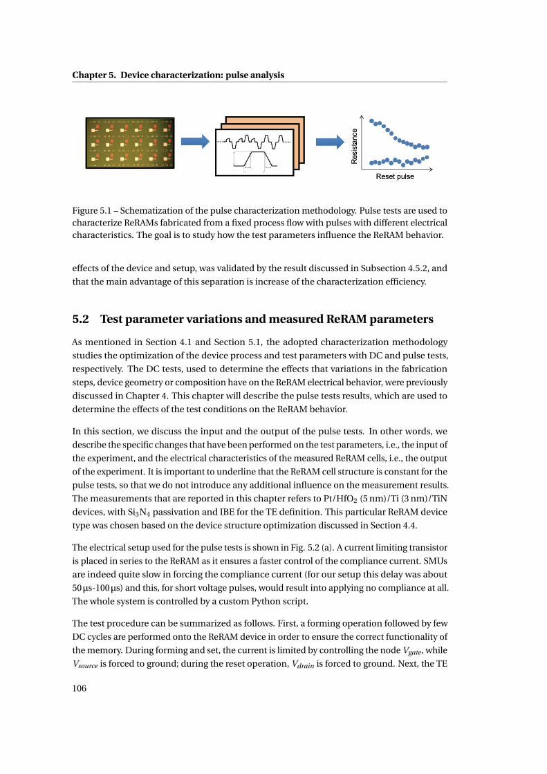
Chapter 5. Device characterization: pulse analysis
Figure 5.1 – Schematization of the pulse characterization methodology. Pulse tests are used tocharacterize ReRAMs fabricated from a fixed process flow with pulses with different electricalcharacteristics. The goal is to study how the test parameters influence the ReRAM behavior.
effects of the device and setup, was validated by the result discussed in Subsection 4.5.2, and
that the main advantage of this separation is increase of the characterization efficiency.
5.2 Test parameter variations and measured ReRAM parameters
As mentioned in Section 4.1 and Section 5.1, the adopted characterization methodology
studies the optimization of the device process and test parameters with DC and pulse tests,
respectively. The DC tests, used to determine the effects that variations in the fabrication
steps, device geometry or composition have on the ReRAM electrical behavior, were previously
discussed in Chapter 4. This chapter will describe the pulse tests results, which are used to
determine the effects of the test conditions on the ReRAM behavior.
In this section, we discuss the input and the output of the pulse tests. In other words, we
describe the specific changes that have been performed on the test parameters, i.e., the input of
the experiment, and the electrical characteristics of the measured ReRAM cells, i.e., the output
of the experiment. It is important to underline that the ReRAM cell structure is constant for the
pulse tests, so that we do not introduce any additional influence on the measurement results.
The measurements that are reported in this chapter refers to Pt/HfO2 (5 nm)/Ti (3 nm)/TiN
devices, with Si3N4 passivation and IBE for the TE definition. This particular ReRAM device
type was chosen based on the device structure optimization discussed in Section 4.4.
The electrical setup used for the pulse tests is shown in Fig. 5.2 (a). A current limiting transistor
is placed in series to the ReRAM as it ensures a faster control of the compliance current. SMUs
are indeed quite slow in forcing the compliance current (for our setup this delay was about
50μs-100μs) and this, for short voltage pulses, would result into applying no compliance at all.
The whole system is controlled by a custom Python script.
The test procedure can be summarized as follows. First, a forming operation followed by few
DC cycles are performed onto the ReRAM device in order to ensure the correct functionality of
the memory. During forming and set, the current is limited by controlling the node Vgate, while
Vsource is forced to ground; during the reset operation, Vdrain is forced to ground. Next, the TE
106
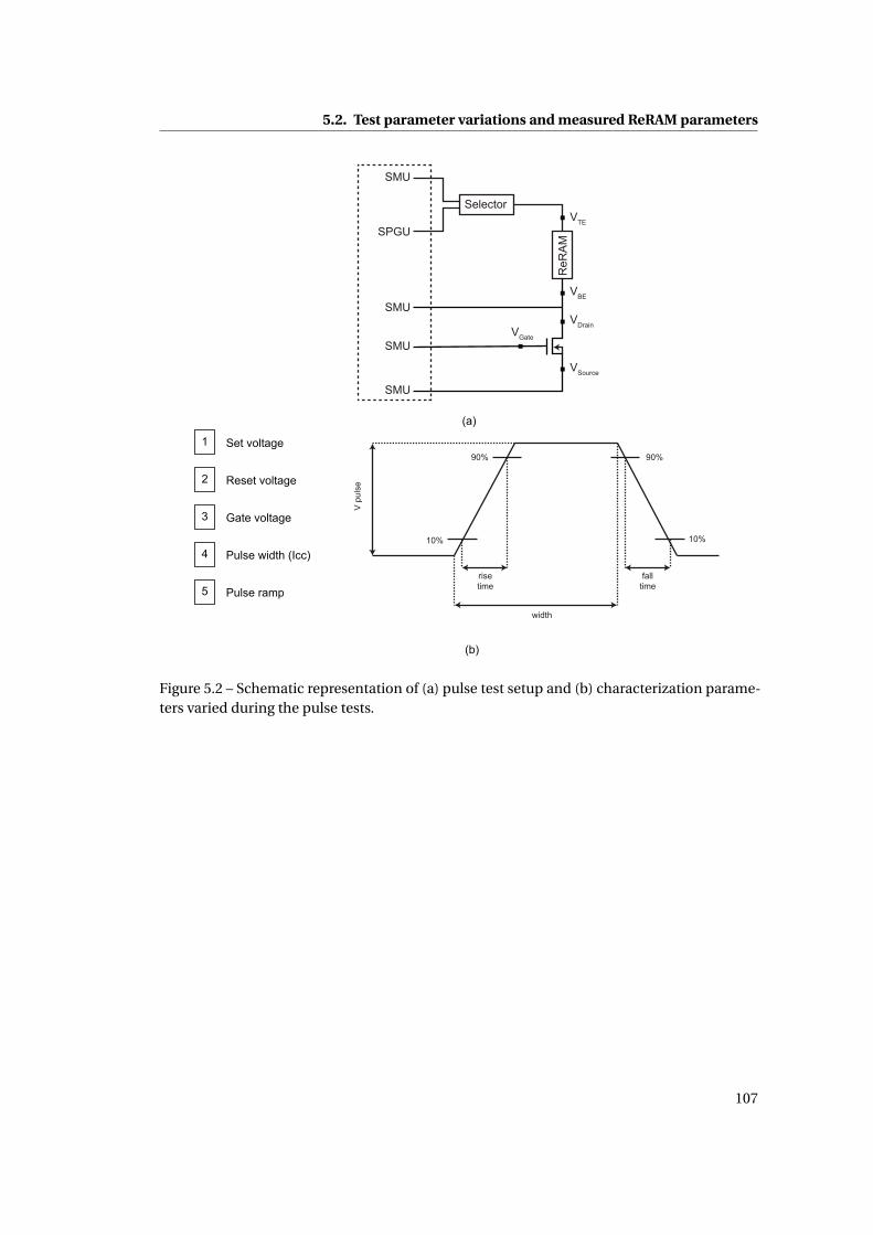
5.2. Test parameter variations and measured ReRAM parameters
Figure 5.2 – Schematic representation of (a) pulse test setup and (b) characterization parame-ters varied during the pulse tests.
107

Chapter 5. Device characterization: pulse analysis
Test variations Measured quantities
Set pulse voltage LRS medianReset pulse voltage HRS medianGate voltage (i.e., current compliance) LRS BERPulse width HRS BERPulse slope
Table 5.1 – Test variations and measured quantities for the pulse tests.
receives a sequence of reset and set pulses. During the set pulse, the Vgate node controls the
compliance current through the transistor, while the Vsource is set to ground. During the reset
pulse, Vgate node is set to 0 V, and the Vdrain node is forced to ground. After the sequence of the
write operations, the test continues with a reset and set pulse coupled with DC read ramps,
which are used to evaluate the device resistances. The test continues then with another series
of write operations, and the procedure repeats itself until the end of the test.
The details of the test methodology, such as the setup used, the data treatment functions, the
structure of the obtained database and the data analysis functions are reported in Appendix A.
The list of the test condition variations and the electrical quantities measured during the pulse
tests are reported in Table 5.1. We modify the test parameters, as shown in Fig 5.2 (b), by
changing the set voltage, the reset voltage, the gate voltage of the current limiting transistor
(which controls the current compliance), the pulse width and the pulse slope (i.e., the pulse
rise and fall time, measured in percentage with respect to the pulse width). The measured
quantities during the pulse tests, represented in Fig. 5.3, are the median values of the LRS
and HRS, and the final BER for the LRS and HRS. A different type of resistance modulation is
obtained by modulating the number of pulses sent to the memory. In this case, the test does
not consist of a sequence of binary switching pulses (a sequence of set and reset operations),
but it relies on sending the same pulse several times to the memory device. This method, as it
is quite different from the normal pulse measurements, is discussed exclusively in Section 5.6.
In the pulse-result database, we reported more than 500 ReRAMs tests. Normally, each test
corresponds to 500 or more set and reset cycles. We tried to test the input domain as completely
as possible, especially the factors which strongly influence the resistance sates. It should be
highlighted that here by "input domain" we refer to the input parameters that allow obtaining
acceptable memory performances. This has been set arbitrarily by considering as acceptable
the devices with a final BER smaller than 20%. This section exclusively discusses the tests
from devices with an acceptable BER (about 330 memory tests), as only these tests have been
considered to study the dependence of the resistance states with respect to the test parameters,
and to extract a compact model that describes the cell behavior (Section 5.5). A discussion
of the totality of the test inputs, as well as the failure analysis for the devices, is reported in
Section 5.4.
108
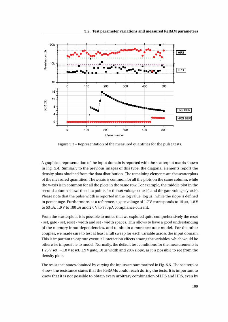
5.2. Test parameter variations and measured ReRAM parameters
Figure 5.3 – Representation of the measured quantities for the pulse tests.
A graphical representation of the input domain is reported with the scatterplot matrix shown
in Fig. 5.4. Similarly to the previous images of this type, the diagonal elements report the
density plots obtained from the data distribution. The remaining elements are the scatterplots
of the measured quantities. The x-axis is common for all the plots on the same column, while
the y-axis is in common for all the plots in the same row. For example, the middle plot in the
second column shows the data points for the set voltage (x-axis) and the gate voltage (y-axis).
Please note that the pulse width is reported in the log value [log μs], while the slope is defined
in percentage. Furthermore, as a reference, a gate voltage of 1.7 V corresponds to 15μA, 1.8 V
to 53μA, 1.9 V to 180μA and 2.0 V to 730μA compliance current.
From the scatterplots, it is possible to notice that we explored quite comprehensively the reset
- set, gate - set, reset - width and set - width spaces. This allows to have a good understanding
of the memory input dependencies, and to obtain a more accurate model. For the other
couples, we made sure to test at least a full sweep for each variable across the input domain.
This is important to capture eventual interaction effects among the variables, which would be
otherwise impossible to model. Normally, the default test conditions for the measurements is
1.25 V set, −1.8 V reset, 1.9 V gate, 10μs width and 20% slope, as it is possible to see from the
density plots.
The resistance states obtained by varying the inputs are summarized in Fig. 5.5. The scatterplot
shows the resistance states that the ReRAMs could reach during the tests. It is important to
know that it is not possible to obtain every arbitrary combination of LRS and HRS, even by
109
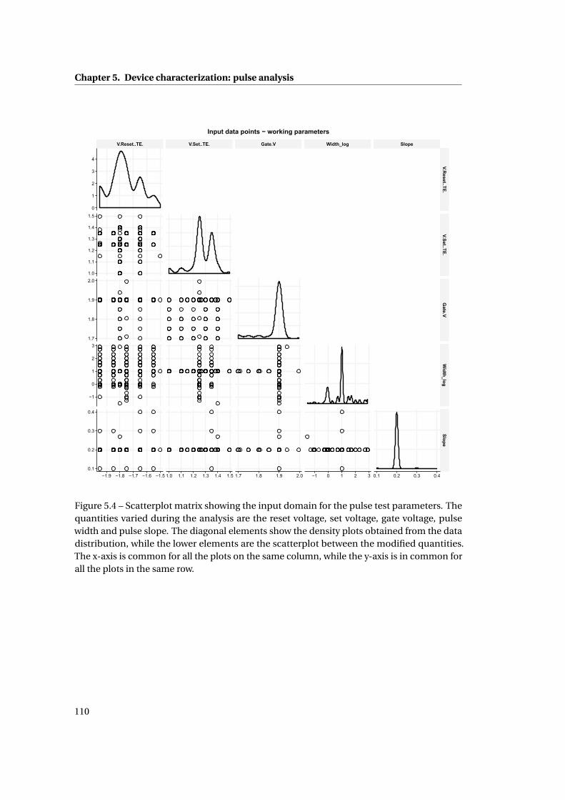
Chapter 5. Device characterization: pulse analysis
Figure 5.4 – Scatterplot matrix showing the input domain for the pulse test parameters. Thequantities varied during the analysis are the reset voltage, set voltage, gate voltage, pulsewidth and pulse slope. The diagonal elements show the density plots obtained from the datadistribution, while the lower elements are the scatterplot between the modified quantities.The x-axis is common for all the plots on the same column, while the y-axis is in common forall the plots in the same row.
110
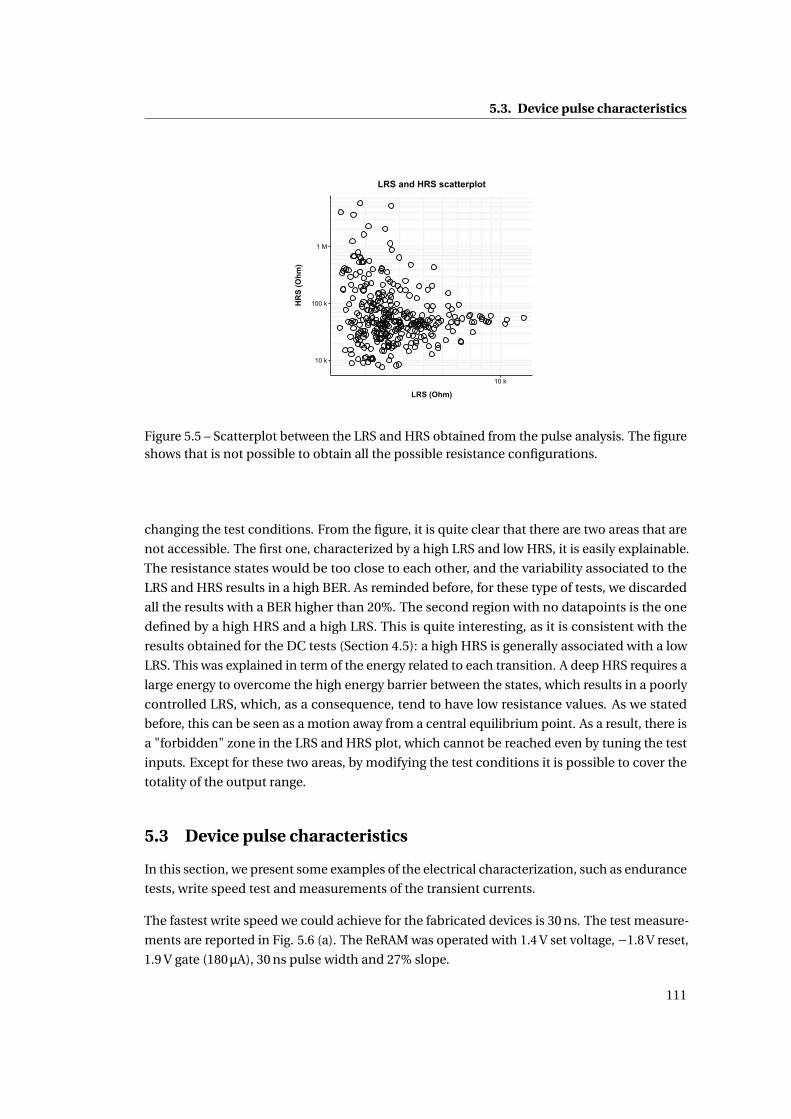
5.3. Device pulse characteristics
Figure 5.5 – Scatterplot between the LRS and HRS obtained from the pulse analysis. The figureshows that is not possible to obtain all the possible resistance configurations.
changing the test conditions. From the figure, it is quite clear that there are two areas that are
not accessible. The first one, characterized by a high LRS and low HRS, it is easily explainable.
The resistance states would be too close to each other, and the variability associated to the
LRS and HRS results in a high BER. As reminded before, for these type of tests, we discarded
all the results with a BER higher than 20%. The second region with no datapoints is the one
defined by a high HRS and a high LRS. This is quite interesting, as it is consistent with the
results obtained for the DC tests (Section 4.5): a high HRS is generally associated with a low
LRS. This was explained in term of the energy related to each transition. A deep HRS requires a
large energy to overcome the high energy barrier between the states, which results in a poorly
controlled LRS, which, as a consequence, tend to have low resistance values. As we stated
before, this can be seen as a motion away from a central equilibrium point. As a result, there is
a "forbidden" zone in the LRS and HRS plot, which cannot be reached even by tuning the test
inputs. Except for these two areas, by modifying the test conditions it is possible to cover the
totality of the output range.
5.3 Device pulse characteristics
In this section, we present some examples of the electrical characterization, such as endurance
tests, write speed test and measurements of the transient currents.
The fastest write speed we could achieve for the fabricated devices is 30 ns. The test measure-
ments are reported in Fig. 5.6 (a). The ReRAM was operated with 1.4 V set voltage, −1.8 V reset,
1.9 V gate (180μA), 30 ns pulse width and 27% slope.
111
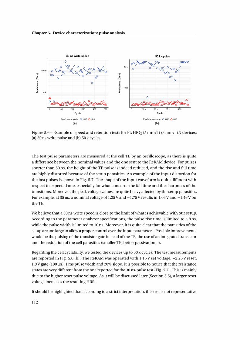
Chapter 5. Device characterization: pulse analysis
Figure 5.6 – Example of speed and retention tests for Pt/HfO2 (5 nm)/Ti (3 nm)/TiN devices:(a) 30 ns write pulse and (b) 50 k cycles.
The test pulse parameters are measured at the cell TE by an oscilloscope, as there is quite
a difference between the nominal values and the one sent to the ReRAM device. For pulses
shorter than 50 ns, the height of the TE pulse is indeed reduced, and the rise and fall time
are highly distorted because of the setup parasitics. An example of the input distortion for
the fast pulses is shown in Fig. 5.7. The shape of the input waveform is quite different with
respect to expected one, especially for what concerns the fall time and the sharpness of the
transitions. Moreover, the peak voltage values are quite heavy affected by the setup parasitics.
For example, at 35 ns, a nominal voltage of 1.25 V and −1.75 V results in 1.06 V and −1.46 V on
the TE.
We believe that a 30 ns write speed is close to the limit of what is achievable with our setup.
According to the parameter analyzer specifications, the pulse rise time is limited to a 8 ns,
while the pulse width is limited to 10 ns. Moreover, it is quite clear that the parasitics of the
setup are too large to allow a proper control over the input parameters. Possible improvements
would be the pulsing of the transistor gate instead of the TE, the use of an integrated transistor
and the reduction of the cell parasitics (smaller TE, better passivation...).
Regarding the cell cyclability, we tested the devices up to 50 k cycles. The test measurements
are reported in Fig. 5.6 (b). The ReRAM was operated with 1.15 V set voltage, −2.25 V reset,
1.9 V gate (180μA), 1 ms pulse width and 20% slope. It is possible to notice that the resistance
states are very different from the one reported for the 30 ns-pulse test (Fig. 5.7). This is mainly
due to the higher reset pulse voltage. As it will be discussed later (Section 5.5), a larger reset
voltage increases the resulting HRS.
It should be highlighted that, according to a strict interpretation, this test is not representative
112
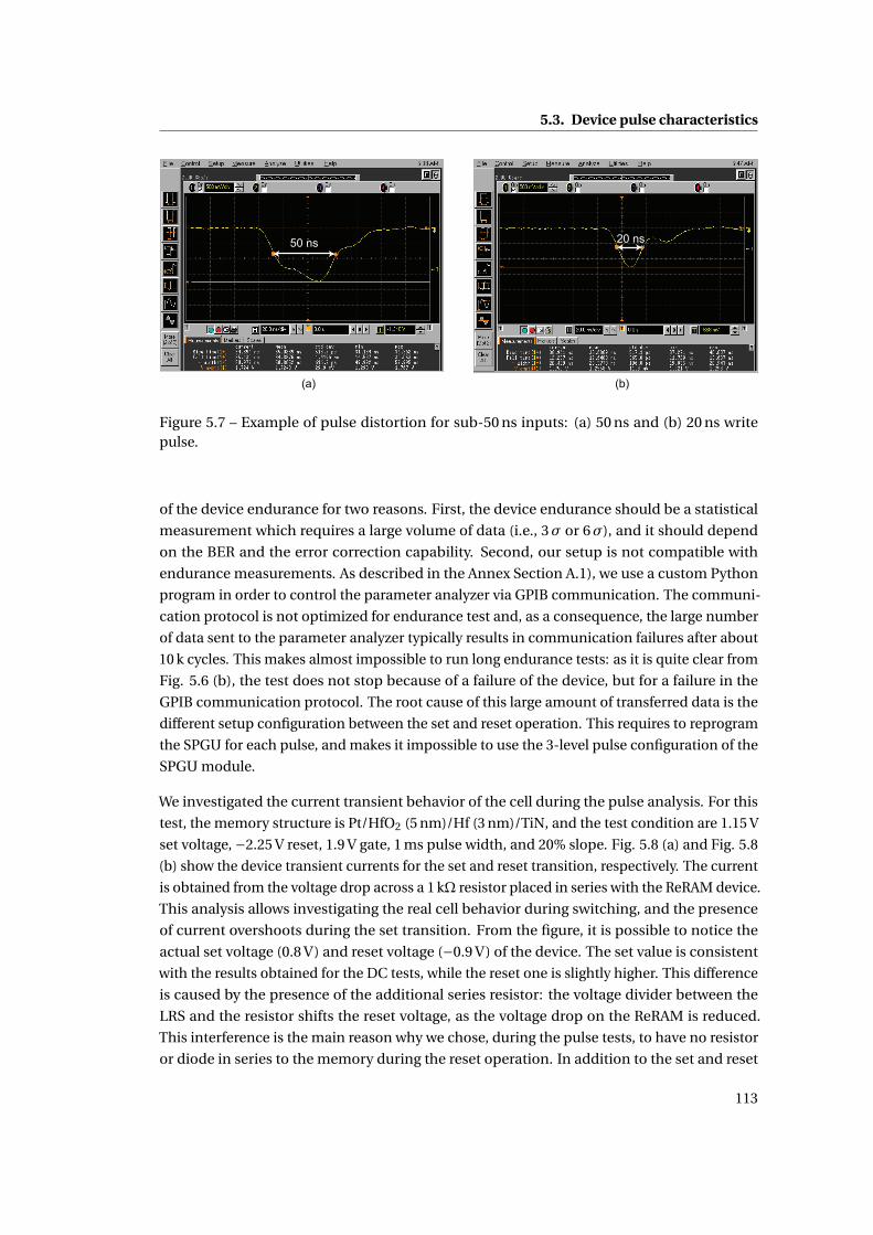
5.3. Device pulse characteristics
Figure 5.7 – Example of pulse distortion for sub-50 ns inputs: (a) 50 ns and (b) 20 ns writepulse.
of the device endurance for two reasons. First, the device endurance should be a statistical
measurement which requires a large volume of data (i.e., 3σ or 6σ), and it should depend
on the BER and the error correction capability. Second, our setup is not compatible with
endurance measurements. As described in the Annex Section A.1), we use a custom Python
program in order to control the parameter analyzer via GPIB communication. The communi-
cation protocol is not optimized for endurance test and, as a consequence, the large number
of data sent to the parameter analyzer typically results in communication failures after about
10 k cycles. This makes almost impossible to run long endurance tests: as it is quite clear from
Fig. 5.6 (b), the test does not stop because of a failure of the device, but for a failure in the
GPIB communication protocol. The root cause of this large amount of transferred data is the
different setup configuration between the set and reset operation. This requires to reprogram
the SPGU for each pulse, and makes it impossible to use the 3-level pulse configuration of the
SPGU module.
We investigated the current transient behavior of the cell during the pulse analysis. For this
test, the memory structure is Pt/HfO2 (5 nm)/Hf (3 nm)/TiN, and the test condition are 1.15 V
set voltage, −2.25 V reset, 1.9 V gate, 1 ms pulse width, and 20% slope. Fig. 5.8 (a) and Fig. 5.8
(b) show the device transient currents for the set and reset transition, respectively. The current
is obtained from the voltage drop across a 1 kΩ resistor placed in series with the ReRAM device.
This analysis allows investigating the real cell behavior during switching, and the presence
of current overshoots during the set transition. From the figure, it is possible to notice the
actual set voltage (0.8 V) and reset voltage (−0.9 V) of the device. The set value is consistent
with the results obtained for the DC tests, while the reset one is slightly higher. This difference
is caused by the presence of the additional series resistor: the voltage divider between the
LRS and the resistor shifts the reset voltage, as the voltage drop on the ReRAM is reduced.
This interference is the main reason why we chose, during the pulse tests, to have no resistor
or diode in series to the memory during the reset operation. In addition to the set and reset
113
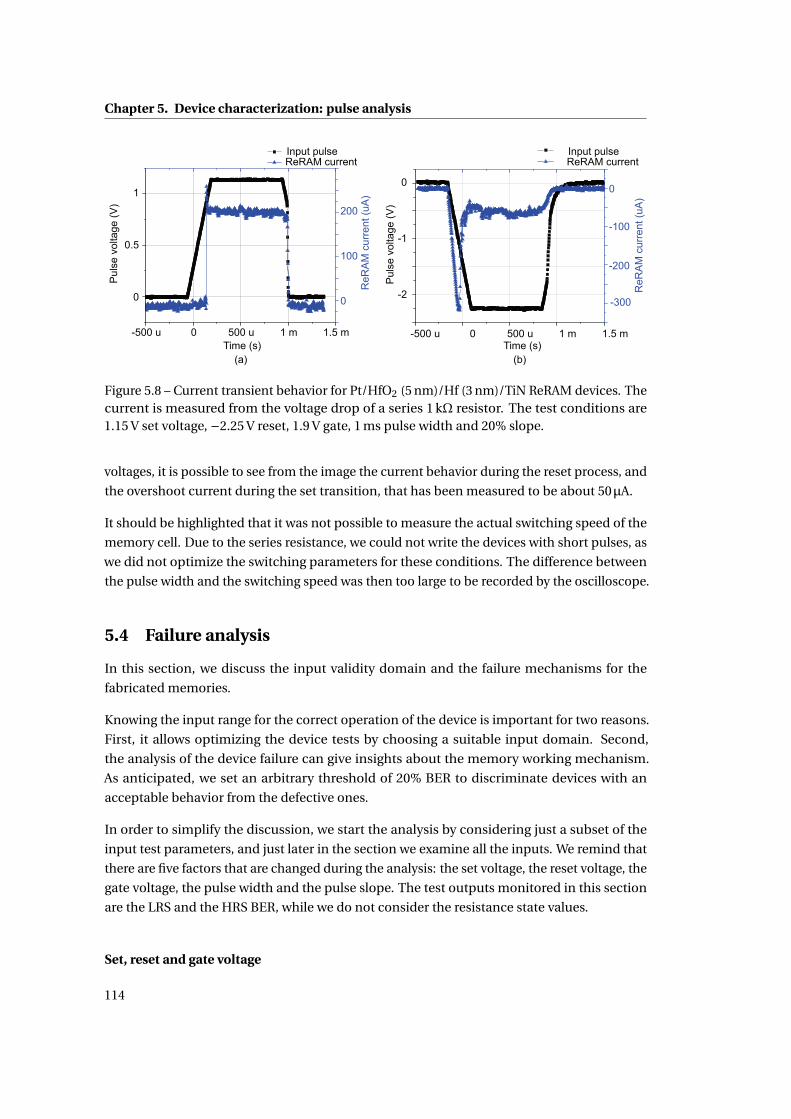
Chapter 5. Device characterization: pulse analysis
Figure 5.8 – Current transient behavior for Pt/HfO2 (5 nm)/Hf (3 nm)/TiN ReRAM devices. Thecurrent is measured from the voltage drop of a series 1 kΩ resistor. The test conditions are1.15 V set voltage, −2.25 V reset, 1.9 V gate, 1 ms pulse width and 20% slope.
voltages, it is possible to see from the image the current behavior during the reset process, and
the overshoot current during the set transition, that has been measured to be about 50μA.
It should be highlighted that it was not possible to measure the actual switching speed of the
memory cell. Due to the series resistance, we could not write the devices with short pulses, as
we did not optimize the switching parameters for these conditions. The difference between
the pulse width and the switching speed was then too large to be recorded by the oscilloscope.
5.4 Failure analysis
In this section, we discuss the input validity domain and the failure mechanisms for the
fabricated memories.
Knowing the input range for the correct operation of the device is important for two reasons.
First, it allows optimizing the device tests by choosing a suitable input domain. Second,
the analysis of the device failure can give insights about the memory working mechanism.
As anticipated, we set an arbitrary threshold of 20% BER to discriminate devices with an
acceptable behavior from the defective ones.
In order to simplify the discussion, we start the analysis by considering just a subset of the
input test parameters, and just later in the section we examine all the inputs. We remind that
there are five factors that are changed during the analysis: the set voltage, the reset voltage, the
gate voltage, the pulse width and the pulse slope. The test outputs monitored in this section
are the LRS and the HRS BER, while we do not consider the resistance state values.
Set, reset and gate voltage
114
5.4. Failure analysis
We start the discussion on the failure analysis by considering the set voltage, the reset voltage,
the gate voltage.
The 3D representation of the input variables with respect to the ReRAM BER is shown in Fig. 5.9
(a). In the graph, the x-axis represents the set voltage pulse, the y-axis the reset voltage pulse,
and the z-axis the gate voltage (i.e., the current compliance control). The data symbols are
coded according to the measured BER: the orange crosses represents the test measurements
with a BER higher than 20%, while the green circles show the test measurements with a BER
smaller that 20%. In this case, the BER value represents both the LRS and the HRS: if a test
shows a LRS BER higher than 20% or a HRS BER higher than 20%, we marked the result as
faulty (BER >20%). As mentioned before, in this case, we limited the input space to just three
variables in order to graphically represent the data in a simple way. More specifically, the
results reported in the figure are only the one with a pulse width larger that 800 ns, and with a
slope of 20%. We fixed these two parameters in order to minimize their negative influence on
the cell performances, allowing to carry on the failure analysis of the three selected factors
(set, reset and gate voltages).
Fig. 5.9 (a) shows that there is a quite clear dependence of the failure rate with respect to the
gate voltage. For values above 2 V the devices do not work properly anymore. This is quite
interesting, as it shows that the device endurance is highly reduced for very energetic state
transitions. It is also clear that the device failure rate increases for reset voltages higher that
−1.5 V. This phenomena is explained by the fact that the reset pulse does not carry enough
energy to switch the resistance state from the LRS to the HRS. Finally, we measured a slight
increase of the device failure for set voltages below 1.1 V, most likely because the set pulse is
not high enough to trigger a state transition.
As a general remark, it should be highlighted that the working domain of the devices is usually
not precisely defined. For example, it is possible to see several test failures at a gate voltage of
1.9 V and a set voltage of 1.25 V. There are two reasons for this behavior. First, the device yield
and variability can influence negatively the test BER, even for optimal input test characteristics.
Second, the graph does not show the number of different tests obtained for each symbol. If for
a specific point there are both a cross and a circle, it means that, for that specific configuration,
there is at least one working and one defective device. This does not mean that the failure
rate of the test is 50%: because equal symbols overlap, the graph does not indicate how many
tests are actually performed for each input configuration. This is quite noticeable especially
along the lines defined by the default inputs values, which are 1.25 V set, −1.8 V reset, 1.9 V
gate, 10μs width and 20% slope. As we performed a large number of tests with these values, it
is very likely to obtain at least a test results with a BER higher that 20%.
A different representation of the data is shown in Fig. 5.9 (b) and Fig. 5.9 (c). The plots show a
2D representation of the 3D space discussed before in Fig. 5.9 (a). The figures are obtained by
projecting all the data points over the gate and reset voltage plane. Moreover, we separated
the BER for the LRS and the HRS, and reported them in Fig. 5.9 (b) and Fig. 5.9 (c), respectively.
115
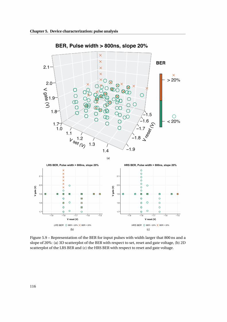
Chapter 5. Device characterization: pulse analysis
V set (V)
1.01.1
1.21.3
1.4V
reset
(V)
V gate (V)
2.0
2.1
BER, Pulse width > 800ns, slope 20%
< 20%
> 20%
BER
(a)
(b) (c)
Figure 5.9 – Representation of the BER for input pulses with width larger that 800 ns and aslope of 20%: (a) 3D scatterplot of the BER with respect to set, reset and gate voltage, (b) 2Dscatterplot of the LRS BER and (c) the HRS BER with respect to reset and gate voltage.
116
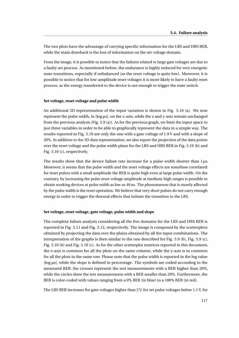
5.4. Failure analysis
The two plots have the advantage of carrying specific information for the LRS and HRS BER,
while the main drawback is the loss of information on the set voltage domain.
From the image, it is possible to notice that the failures related to large gate voltages are due to
a faulty set process. As mentioned before, the endurance is highly reduced for very energetic
state transitions, especially if unbalanced (as the reset voltage is quite low). Moreover, it is
possible to notice that for low-amplitude reset voltages it is more likely to have a faulty reset
process, as the energy transferred to the device is not enough to trigger the state switch.
Set voltage, reset voltage and pulse width
An additional 3D representation of the input variation is shown in Fig. 5.10 (a). We now
represent the pulse width, in [log μs], on the z-axis, while the x and y-axis remain unchanged
from the previous analysis [Fig. 5.9 (a)]. As for the previous graph, we limit the input space to
just three variables in order to be able to graphically represent the data in a simple way. The
results reported in Fig. 5.10 are only the one with a gate voltage of 1.9 V and with a slope of
20%. In addition to the 3D data representation, we also report the projection of the data points
over the reset voltage and the pulse width plane for the LRS and HRS BER in Fig. 5.10 (b) and
Fig. 5.10 (c), respectively.
The results show that the device failure rate increase for a pulse width shorter than 1μs.
Moreover, it seems that the pulse width and the reset voltage effects are somehow correlated:
for reset pulses with a small amplitude the BER is quite high even at large pulse width. On the
contrary, by increasing the pulse reset voltage amplitude at medium-high ranges is possible to
obtain working devices at pulse width as low as 40 ns. The phenomenon that is mostly affected
by the pulse width is the reset operation. We believe that very short pulses do not carry enough
energy in order to trigger the thermal effects that initiate the transition to the LRS.
Set voltage, reset voltage, gate voltage, pulse width and slope
The complete failure analysis considering all the five domains for the LRS and HRS BER is
reported in Fig. 5.11 and Fig. 5.12, respectively. The image is composed by the scatterplots
obtained by projecting the data over the plains obtained by all the input combinations. The
interpretation of the graphs is then similar to the one described for Fig. 5.9 (b), Fig. 5.9 (c),
Fig. 5.10 (b) and Fig. 5.10 (c). As for the other scatterplot matrices reported in this document,
the x-axis is common for all the plots on the same column, while the y-axis is in common
for all the plots in the same row. Please note that the pulse width is reported in the log value
[log μs], while the slope is defined in percentage. The symbols are coded according to the
measured BER: the crosses represent the test measurements with a BER higher than 20%,
while the circles show the test measurements with a BER smaller than 20%. Furthermore, the
BER is color-coded with values ranging from a 0% BER (in blue) to a 100% BER (in red).
The LRS BER increases for gate voltages higher than 2 V, for set pulse voltages below 1.1 V, for
117
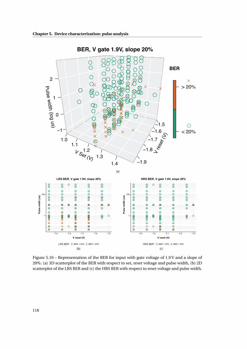
Chapter 5. Device characterization: pulse analysis
V Set (V)
1.01.1
1.21.3
1.4V
reset
(V)
Pulse width (log us)
0
1
2
BER, V gate 1.9V, slope 20%
< 20%
> 20%
BER
(a)
(b) (c)
Figure 5.10 – Representation of the BER for input with gate voltage of 1.9 V and a slope of20%: (a) 3D scatterplot of the BER with respect to set, reset voltage and pulse width, (b) 2Dscatterplot of the LRS BER and (c) the HRS BER with respect to reset voltage and pulse width.
118
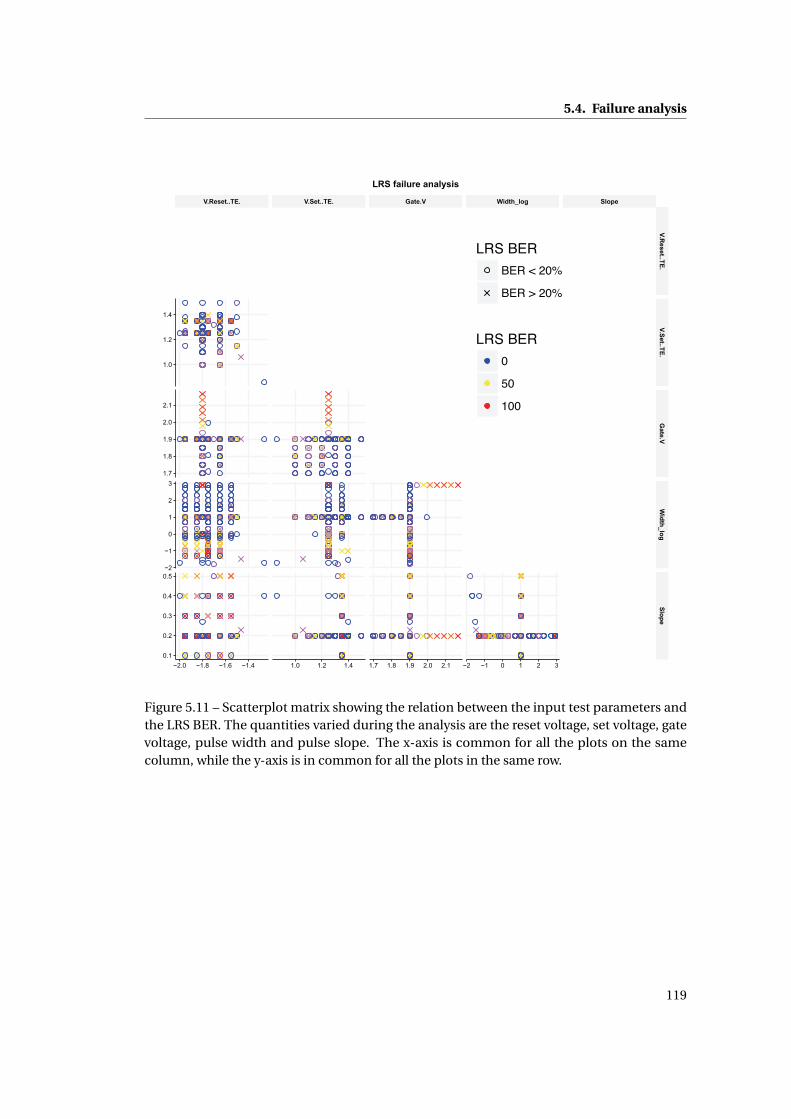
5.4. Failure analysis
LRS BERBER < 20%BER > 20%
LRS BER050100
Figure 5.11 – Scatterplot matrix showing the relation between the input test parameters andthe LRS BER. The quantities varied during the analysis are the reset voltage, set voltage, gatevoltage, pulse width and pulse slope. The x-axis is common for all the plots on the samecolumn, while the y-axis is in common for all the plots in the same row.
119
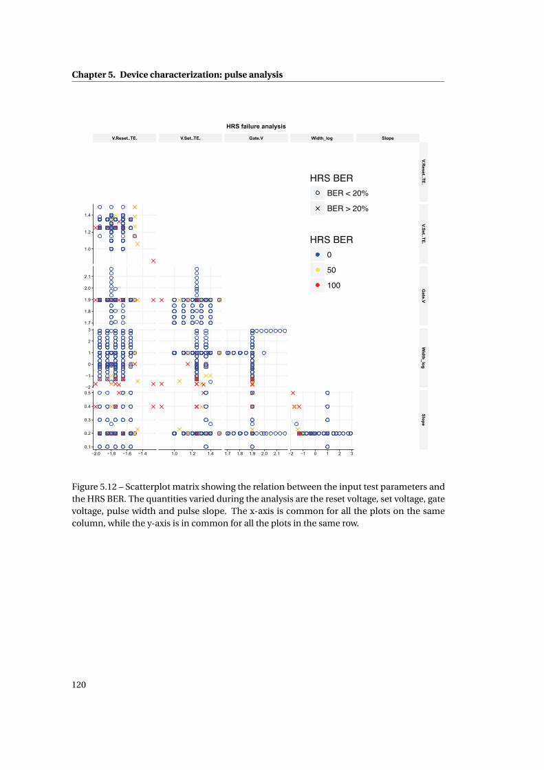
Chapter 5. Device characterization: pulse analysis
HRS BERBER < 20%BER > 20%
HRS BER050100
Figure 5.12 – Scatterplot matrix showing the relation between the input test parameters andthe HRS BER. The quantities varied during the analysis are the reset voltage, set voltage, gatevoltage, pulse width and pulse slope. The x-axis is common for all the plots on the samecolumn, while the y-axis is in common for all the plots in the same row.
120
5.5. Influence of the test parameters on the ReRAM resistance states
pulse width shorter than 1μs and slope values of more than 40%. The reset pulse voltage does
not have a clear influence on the LRS BER. These failures are generally attributed to the set
process. A low set pulse cannot build up enough field into the device to trigger the switching
mechanism. Moreover, once the set process is initiated, it requires enough time to trigger the
resistance change. Very short pulses, or pulses with a limited time above the set voltage (i.e.,
with a large slope) may result in the set process failure. Finally, the impact of the gate voltage
is quite counter-intuitive. We may need more data to clearly access this phenomenon, but
we think that the BER increase is related to the very high energy associated to the set state
transition, especially if it is associated with a weak reset.
The HRS BER increases for set pulses below 1.1 V, and for reset pulses higher that −1.5 V.
Moreover, there is an increasing number of failures for pulse width shorter than 100 ns and for
slopes above 40%. The gate voltage does not appear to have a clear influence on the HRS BER.
Complementarily to what has been discussed in the previous paragraph, these failures are
attributed to the reset process. A low reset pulse (in absolute value) cannot build up enough
current into the device to trigger the switching mechanism, and short pulses, or pulses with a
limited time above the reset voltage (i.e., with a large slope) may result in the reset process
failure. Finally, the impact of a low set voltage is quite counter-intuitive. Similarly to what
discussed for the LRS, we believe that the BER increase is related to an unbalanced switching
mechanism, as the set voltage is too low with respect to the reset one.
As a final remark, we should comment on the distinction between the LRS and HRS BER.
For very weak transitions (e.g., low set and reset voltage pulses), it may be impossible to
discriminate between a LRS or a HRS failure. The resistance states are extremely close to each
other, and the device resistance gets usually stacked at a medium-level value. According to the
definitions of the resistance thresholds, this could be interpreted either as a LRS failure or a
HRS failure. An example of this phenomenon is discussed in Section 5.5, while describing Fig.
5.13. Nevertheless, these are limited cases, so they do not invalidate the discussion presented
above.
5.5 Influence of the test parameters on the ReRAM resistance states
In this section, we discuss how the test parameters affect the resistance states. In the literature,
the modulation of the resistance state by changing some of the setup characteristics, such
as the reset pulse voltage and duration, is shown for example in [10]. The main difference
compared to this work is that we considered a larger number of test parameters for a larger
number of test conditions. This allows us to discuss the statistical significance of each input on
the LRS and HRS, and to evaluate and model the effects of the setup parameter interactions.
The section is divided as follows. First, in Subsection 5.5.1, we show some examples of input
modulation and we qualitatively discuss the effects on the LRS and HRS. Then, in Subsection
5.5.2, we perform an analysis of variance to determine which input mainly contributes to
each state. Finally, in Subsection 5.5.3, we propose an empirical model that relates the test
121
Chapter 5. Device characterization: pulse analysis
parameters to the resistance states.
As discussed before, the analytical part of this section (Subsection 5.5.2 and Subsection 5.5.3)
is obtained by analyzing exclusively the test results with a BER lower than 20%.
5.5.1 Qualitative description
The following text is divided in paragraphs according to the modified test inputs.
Set and reset pulse voltage
The effect of the set and reset pulse voltage on the resistance states is summarized in Fig.
5.13. Fig. 5.13 (a) reports the test results obtained on a single device with 1.9 V gate voltage,
10μs pulse width and 20% slope. The reset pulse level changes every 2 k cycles with values
of −1.95 V, −1.8 V, −1.65 V, −1.5 V. The set pulse, color coded in the image, varies every 500
cycles with values of 1.5 V, 1.38 V, 1.26 V and 1.15 V. The results show quite clearly that the reset
pulse have a large influence on the HRS: as the reset pulse amplitude decreases, the HRS
decreases accordingly. A large reset pulse allows indeed to induce more energy in the reset
process, which results in a higher HRS. The set pulse impacts mostly the LRS value: as the
pulse decreases the LRS increases, as there is less energy induced into the set operation. It
is quite interesting to notice that this influence is not constant over all the test. It is indeed
almost zero for very large HRS, while it is amplified for the regions with a low HRS. We think
that this results from the relation between the HRS and the LRS. As discussed both for the
DC tests (Subsection 4.5.2) and the pulse-result summary (Section 5.5), the LRS and the HRS
influence each other. In particular, a memory with a very high HRS also shows a very low LRS.
We believe this intra-state relation limits, for some operating regions, the control of the test
inputs over the resistance state. As a consequence, we think that for multi-bit applications it
would be more beneficial to modulate just one of the resistance state, and not both.
Fig. 5.13 (b) shows the modulation of the HRS for a set pulse voltage of 1.38 V. According
to the reset pulse amplitude, color coded in the figure, the HRS changes both in value and
distribution. Large HRS values are generally associated with a much larger resistance variability.
The variation of the set pulse does not influence much the HRS values. The same plot including
all the set voltages, and not just 1.38 V, differs exclusively in the distribution tails (not shown).
According to the results, it seems feasible to store multiple resistance levels in the same device.
Considering also the LRS, the memory can reach at least 4 defined resistance levels (the LRS,
and the red, the blue and the black HRS from the image).
Fig. 5.13 (c) shows the modulation of the set voltage with a reset pulse voltage of −1.8 V. The
figure highlights how the LRS increases for a decrease of the set pulse amplitude.
Reset pulse voltage and pulse width
122
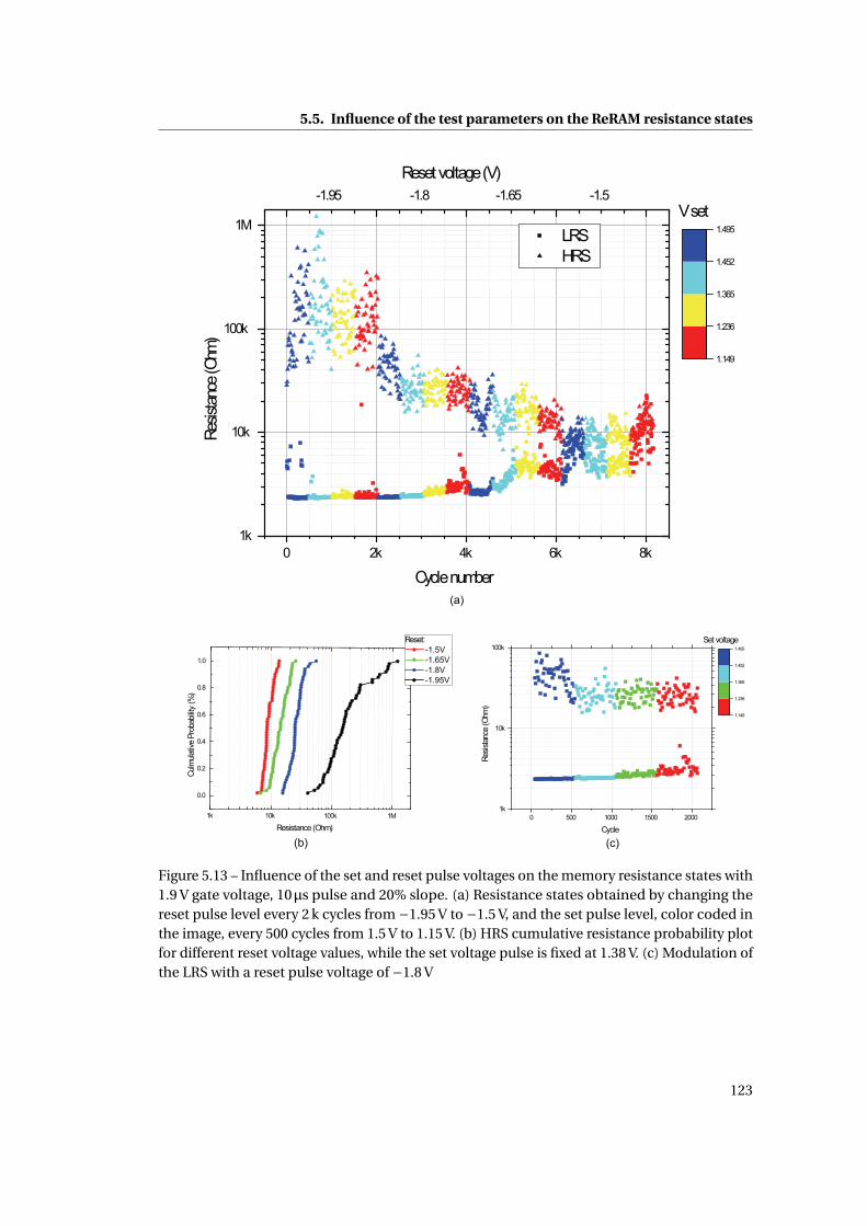
5.5. Influence of the test parameters on the ReRAM resistance states
Figure 5.13 – Influence of the set and reset pulse voltages on the memory resistance states with1.9 V gate voltage, 10μs pulse and 20% slope. (a) Resistance states obtained by changing thereset pulse level every 2 k cycles from −1.95 V to −1.5 V, and the set pulse level, color coded inthe image, every 500 cycles from 1.5 V to 1.15 V. (b) HRS cumulative resistance probability plotfor different reset voltage values, while the set voltage pulse is fixed at 1.38 V. (c) Modulation ofthe LRS with a reset pulse voltage of −1.8 V
123
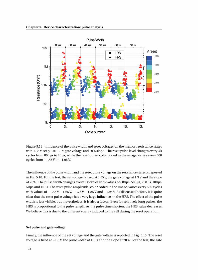
Chapter 5. Device characterization: pulse analysis
Figure 5.14 – Influence of the pulse width and reset voltages on the memory resistance stateswith 1.35 V set pulse, 1.9 V gate voltage and 20% slope. The reset pulse level changes every 3 kcycles from 800μs to 10μs, while the reset pulse, color coded in the image, varies every 500cycles from −1.55 V to −1.95 V.
The influence of the pulse width and the reset pulse voltage on the resistance states is reported
in Fig. 5.10. For the test, the set voltage is fixed at 1.35 V, the gate voltage at 1.9 V and the slope
at 20%. The pulse width changes every 3 k cycles with values of 800μs, 500μs, 200μs, 100μs,
50μs and 10μs. The reset pulse amplitude, color coded in the image, varies every 500 cycles
with values of −1.55 V, −1.65 V, −1.75 V, −1.85 V and −1.95 V. As discussed before, it is quite
clear that the reset pulse voltage has a very large influence on the HRS. The effect of the pulse
width is less visible, but, nevertheless, it is also a factor. Even for relatively long pulses, the
HRS is proportional to the pulse length. As the pulse time shorten, the HRS value decreases.
We believe this is due to the different energy induced to the cell during the reset operation.
Set pulse and gate voltage
Finally, the influence of the set voltage and the gate voltage is reported in Fig. 5.15. The reset
voltage is fixed at −1.8 V, the pulse width at 10μs and the slope at 20%. For the test, the gate
124
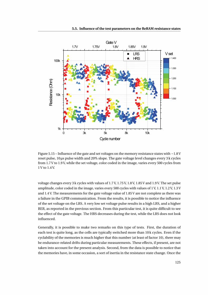
5.5. Influence of the test parameters on the ReRAM resistance states
Figure 5.15 – Influence of the gate and set voltages on the memory resistance states with −1.8 Vreset pulse, 10μs pulse width and 20% slope. The gate voltage level changes every 3 k cyclesfrom 1.7 V to 1.9 V, while the set voltage, color coded in the image, varies every 500 cycles from1 V to 1.4 V.
voltage changes every 3 k cycles with values of 1.7 V, 1.75 V, 1.8 V, 1.85 V and 1.9 V. The set pulse
amplitude, color coded in the image, varies every 500 cycles with values of 1 V, 1.1 V, 1.2 V, 1.3 V
and 1.4 V. The measurements for the gate voltage value of 1.85 V are not complete as there was
a failure in the GPIB communication. From the results, it is possible to notice the influence
of the set voltage on the LRS. A very low set voltage pulse results in a high LRS, and a higher
BER, as reported in the previous section. From this particular test, it is quite difficult to see
the effect of the gate voltage. The HRS decreases during the test, while the LRS does not look
influenced.
Generally, it is possible to make two remarks on this type of tests. First, the duration of
each test is quite long, as the cells are typically switched more than 10 k cycles. Even if the
cyclability of the memories is much higher that this number (at least of factor 10), there may
be endurance-related drifts during particular measurements. These effects, if present, are not
taken into account for the present analysis. Second, from the data is possible to notice that
the memories have, in some occasion, a sort of inertia in the resistance state change. Once the
125
Chapter 5. Device characterization: pulse analysis
test input conditions are changed, it may take several cycles to stabilize the cell to the new
conditions. This is particularly evident if the input is changed from a high energy transition
to a low level one. For example, if the reset pulse changes from −1.9 V to −1.5 V, the first HRS
measurements for the new input condition will still be quite high.
5.5.2 Analysis of variance
We performed an analysis of variance on the measurement results to determine which input
affects more each resistance state. Table 5.2 and Table 5.3 report the ANOVA results considering
the set voltage, reset voltage, gate voltage, pulse width and pulse slope with respect to the
logarithm of the LRS and HRS, respectively. The details about the table interpretation are
reported in the Annex Section A.4. In summary, the significant codes in the last column can
be used in order to determine whether an input influences the resistance state or not. We
decided to use the logarithmic value of the resistances because, according to the diagnostic
plots, the result of the analysis are much more reliable. In particular, for the nominal LRS and
HRS values, the data are quite heteroscedastic, and the residuals are not normal.
From Table 5.2 it looks quite clear that the log(LRS) is mainly influenced by the set voltage
and the gate voltage. The p-values of the other inputs are quite high, so they do not clearly
contribute in defining the resistance value. This is quite expected, as the set voltage pulse and
the current compliance are the main controllers of the set process. As demonstrated in Chapter
4 for the analysis, the set pulse voltage triggers the set process, while the compliance current
controls the second part of the transition to the HRS. Despite the non-optimal compliance
control of the setup used, the gate voltage is still an important factor for the LRS definition.
Interestingly, the reset pulse does not clearly influence the LRS: this is quite promising, as
it suggests the possibility to freely change the reset pulse without influencing the LRS. The
same is valid for the pulse width and slope. We believe that the pulse width does not influence
the LRS as the phenomena involved are not strictly defined by thermal processes (i.e., heat
generation). The set process is first triggered by field effects, and then controlled by the
maximum current value flowing into the device, and not much by the total time for which the
current is applied.
Table 5.3 shows the analysis results for the log(HRS). The input can be classified into two
groups, according to their influence on the resistance value. The most influencing factors are
the reset voltage and the pulse width. This may be expected, as the reset process is mainly
controlled by the reset pulse voltage. Moreover, considering the reset as a thermally assisted
process, the pulse time influence is quite high. The other inputs have a smaller control over
the HRS. The p-values are above 5%, which is about the threshold used in engineering to
define a factor as an acceptable one. As a consequence, we can state that the set voltage,
the gate voltage and the pulse slope do not strongly affect the resistance value. Nevertheless,
probably because of the relation between the resistant states, these factors play a secondary
and minor role in the HRS definition.
126
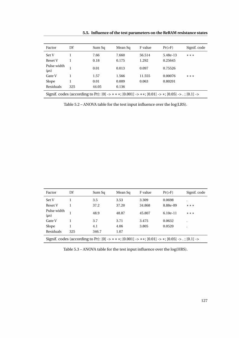
5.5. Influence of the test parameters on the ReRAM resistance states
Factor Df Sum Sq Mean Sq F value Pr(>F) Signif. code
Set V 1 7.66 7.660 56.514 5.48e-13 ∗∗∗Reset V 1 0.18 0.175 1.292 0.25645
Pulse width(μs)
1 0.01 0.013 0.097 0.75526
Gate V 1 1.57 1.566 11.555 0.00076 ∗∗∗Slope 1 0.01 0.009 0.063 0.80201
Residuals 325 44.05 0.136
Signif. codes (according to Pr): [0] -> ∗∗∗; [0.001] -> ∗∗; [0.01] -> ∗; [0.05] -> . ; [0.1] ->
Table 5.2 – ANOVA table for the test input influence over the log(LRS).
Factor Df Sum Sq Mean Sq F value Pr(>F) Signif. code
Set V 1 3.5 3.53 3.309 0.0698 .
Reset V 1 37.2 37.20 34.868 8.88e-09 ∗∗∗Pulse width(μs)
1 48.9 48.87 45.807 6.10e-11 ∗∗∗Gate V 1 3.7 3.71 3.475 0.0632 .
Slope 1 4.1 4.06 3.805 0.0520 .
Residuals 325 346.7 1.07
Signif. codes (according to Pr): [0] -> ∗∗∗; [0.001] -> ∗∗; [0.01] -> ∗; [0.05] -> . ; [0.1] ->
Table 5.3 – ANOVA table for the test input influence over the log(HRS).
127
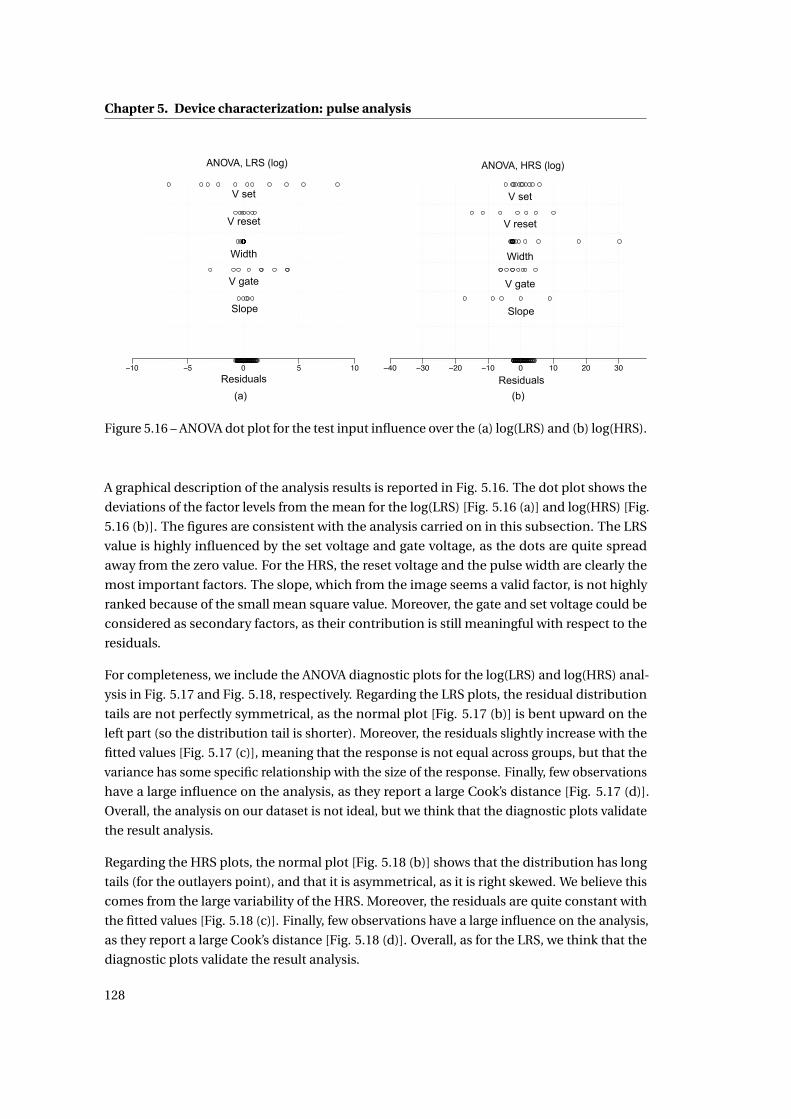
Chapter 5. Device characterization: pulse analysis
Figure 5.16 – ANOVA dot plot for the test input influence over the (a) log(LRS) and (b) log(HRS).
A graphical description of the analysis results is reported in Fig. 5.16. The dot plot shows the
deviations of the factor levels from the mean for the log(LRS) [Fig. 5.16 (a)] and log(HRS) [Fig.
5.16 (b)]. The figures are consistent with the analysis carried on in this subsection. The LRS
value is highly influenced by the set voltage and gate voltage, as the dots are quite spread
away from the zero value. For the HRS, the reset voltage and the pulse width are clearly the
most important factors. The slope, which from the image seems a valid factor, is not highly
ranked because of the small mean square value. Moreover, the gate and set voltage could be
considered as secondary factors, as their contribution is still meaningful with respect to the
residuals.
For completeness, we include the ANOVA diagnostic plots for the log(LRS) and log(HRS) anal-
ysis in Fig. 5.17 and Fig. 5.18, respectively. Regarding the LRS plots, the residual distribution
tails are not perfectly symmetrical, as the normal plot [Fig. 5.17 (b)] is bent upward on the
left part (so the distribution tail is shorter). Moreover, the residuals slightly increase with the
fitted values [Fig. 5.17 (c)], meaning that the response is not equal across groups, but that the
variance has some specific relationship with the size of the response. Finally, few observations
have a large influence on the analysis, as they report a large Cook’s distance [Fig. 5.17 (d)].
Overall, the analysis on our dataset is not ideal, but we think that the diagnostic plots validate
the result analysis.
Regarding the HRS plots, the normal plot [Fig. 5.18 (b)] shows that the distribution has long
tails (for the outlayers point), and that it is asymmetrical, as it is right skewed. We believe this
comes from the large variability of the HRS. Moreover, the residuals are quite constant with
the fitted values [Fig. 5.18 (c)]. Finally, few observations have a large influence on the analysis,
as they report a large Cook’s distance [Fig. 5.18 (d)]. Overall, as for the LRS, we think that the
diagnostic plots validate the result analysis.
128
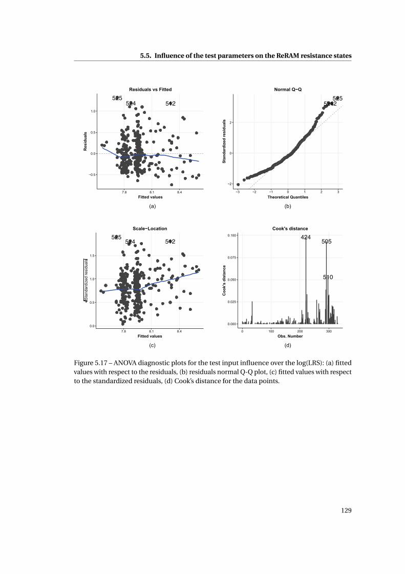
5.5. Influence of the test parameters on the ReRAM resistance states
525524 512
525524512
525 524 512 424 505
510
Figure 5.17 – ANOVA diagnostic plots for the test input influence over the log(LRS): (a) fittedvalues with respect to the residuals, (b) residuals normal Q-Q plot, (c) fitted values with respectto the standardized residuals, (d) Cook’s distance for the data points.
129
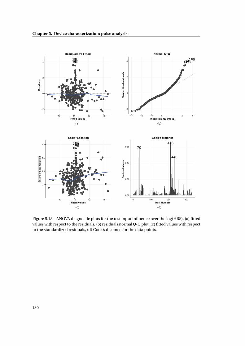
Chapter 5. Device characterization: pulse analysis
116143142 116143142
116143142 41370
443
Figure 5.18 – ANOVA diagnostic plots for the test input influence over the log(HRS), (a) fittedvalues with respect to the residuals, (b) residuals normal Q-Q plot, (c) fitted values with respectto the standardized residuals, (d) Cook’s distance for the data points.
130
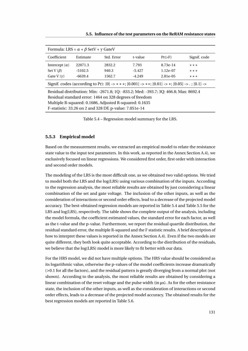
5.5. Influence of the test parameters on the ReRAM resistance states
Formula: LRS = α + β SetV + γ GateV
Coefficient Estimate Std. Error t-value Pr(>F) Signif. code
Intercept (α) 22071.3 2832.2 7.793 8.73e-14 ∗∗∗Set V (β) -5102.5 940.3 -5.427 1.12e-07 ∗∗∗Gate V (γ) -6639.4 1562.7 -4.249 2.81e-05 ∗∗∗Signif. codes (according to Pr): [0] -> ∗∗∗; [0.001] -> ∗∗; [0.01] -> ∗; [0.05] -> . ; [0.1] ->
Residual distribution: Min: -2671.8; 1Q: -833.2; Med: -393.7; 3Q: 466.8; Max: 8692.4Residual standard error: 1464 on 328 degrees of freedomMultiple R-squared: 0.1686, Adjusted R-squared: 0.1635F-statistic: 33.26 on 2 and 328 DF, p-value: 7.051e-14
Table 5.4 – Regression model summary for the LRS.
5.5.3 Empirical model
Based on the measurement results, we extracted an empirical model to relate the resistance
state value to the input test parameters. In this work, as reported in the Annex Section A.4), we
exclusively focused on linear regressions. We considered first order, first order with interaction
and second order models.
The modeling of the LRS is the most difficult one, as we obtained two valid options. We tried
to model both the LRS and the log(LRS) using various combination of the inputs. According
to the regression analysis, the most reliable results are obtained by just considering a linear
combination of the set and gate voltage. The inclusion of the other inputs, as well as the
consideration of interactions or second order effects, lead to a decrease of the projected model
accuracy. The best-obtained regression models are reported in Table 5.4 and Table 5.5 for the
LRS and log(LRS), respectively. The table shows the complete output of the analysis, including
the model formula, the coefficient estimated values, the standard error for each factor, as well
as the t-value and the p-value. Furthermore, we report the residual quartile distribution, the
residual standard error, the multiple R-squared and the F statistic results. A brief description of
how to interpret these values is reported in the Annex Section A.4). Even if the two models are
quite different, they both look quite acceptable. According to the distribution of the residuals,
we believe that the log(LRS) model is more likely to fit better with our data.
For the HRS model, we did not have multiple options. The HRS value should be considered as
its logarithmic value, otherwise the p-values of the model coefficients increase dramatically
(>0.1 for all the factors), and the residual pattern is greatly diverging from a normal plot (not
shown). According to the analysis, the most reliable results are obtained by considering a
linear combination of the reset voltage and the pulse width (in μs). As for the other resistance
state, the inclusion of the other inputs, as well as the consideration of interactions or second
order effects, leads to a decrease of the projected model accuracy. The obtained results for the
best regression models are reported in Table 5.6.
131
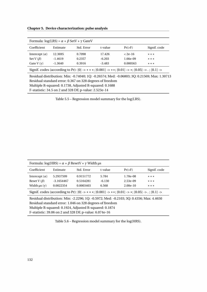
Chapter 5. Device characterization: pulse analysis
Formula: log(LRS) = α + β SetV + γ GateV
Coefficient Estimate Std. Error t-value Pr(>F) Signif. code
Intercept (α) 12.3695 0.7098 17.426 < 2e-16 ∗∗∗Set V (β) -1.4619 0.2357 -6.203 1.66e-09 ∗∗∗Gate V (γ) -1.3640 0.3916 -3.483 0.000563 ∗∗∗Signif. codes (according to Pr): [0] -> ∗∗∗; [0.001] -> ∗∗; [0.01] -> ∗; [0.05] -> . ; [0.1] ->
Residual distribution: Min: -0.74040; 1Q: -0.26574; Med: -0.06803; 3Q: 0.21569; Max: 1.30713Residual standard error: 0.367 on 328 degrees of freedomMultiple R-squared: 0.1738, Adjusted R-squared: 0.1688F-statistic: 34.5 on 2 and 328 DF, p-value: 2.523e-14
Table 5.5 – Regression model summary for the log(LRS).
Formula: log(HRS) = α + β ResetV + γ Width μs
Coefficient Estimate Std. Error t-value Pr(>F) Signif. code
Intercept (α) 5.2937599 0.9151772 5.784 1.70e-08 ∗∗∗Reset V (β) -3.1654467 0.5164281 -6.130 2.53e-09 ∗∗∗Width μs (γ) 0.0022354 0.0003403 6.568 2.00e-10 ∗∗∗Signif. codes (according to Pr): [0] -> ∗∗∗; [0.001] -> ∗∗; [0.01] -> ∗; [0.05] -> . ; [0.1] ->
Residual distribution: Min: -2.2296; 1Q: -0.5972; Med: -0.2103; 3Q: 0.4356; Max: 4.4650Residual standard error: 1.046 on 328 degrees of freedomMultiple R-squared: 0.1924, Adjusted R-squared: 0.1874F-statistic: 39.06 on 2 and 328 DF, p-value: 6.074e-16
Table 5.6 – Regression model summary for the log(HRS).
132

5.6. Pulse number modulation
Figure 5.19 – Calculated coefficients with 2.5% and 97.5% confidence levels for the (a) log(LRS)and (b) log(HRS) models.
The obtained regression coefficients are graphically represented in Fig. 5.19. The rectangle
shows the estimated value of the coefficients, while the error bar reports the 97.5% and 2.5%
coefficient confidence intervals. For the log(LRS) model [Fig. 5.19 (a)], the coefficients for the
intercept, the set voltage and the gate voltage are 12.37, −1.46 and −1.36, while the confidence
intervals are, respectively, [10.97, 13.76], [−1.92, −1.00] and [−2.13, −0.59]. For the log(HRS)
model [Fig. 5.19 (a)], the coefficients for the intercept, the reset voltage and the pulse width are
5.29, −3.16 and 0.00224, while the confidence intervals are, respectively, [3,49, 7.09], [−4.18,
−2.15] and [0.00156, 0.00290]. We should highlight that a small coefficient value does not
automatically imply that the input effect on the resistance state is null. The factor should be
indeed considered with respect to the range and the typical value of the corresponding input.
Finally, for completeness, we report the diagnostic plots in Fig. 5.20 and Fig. 5.21 for the
log(LRS) and the log(HRS) models, respectively. We will not discuss the images, as they are
very similar to the one obtained from the ANOVA analysis reported in Subsection 5.5.2.
5.6 Pulse number modulation
An additional type of resistance modulation has been obtained by controlling the number
of pulses sent to the memory device. In this case, the device is first set to a predetermined
resistance state. Subsequently, a train of reset (or set) pulses are sent to the memory, each
one typically preceded and followed by a read operation. The pulse triggers just a partial
switch operation, allowing to obtain an analog-like resistance behavior. The device resistance
is monitored before and after the pulse application, in order to ensure that the pulse induces a
change in the resistance state and that there are no time-related drift effects in between the
133
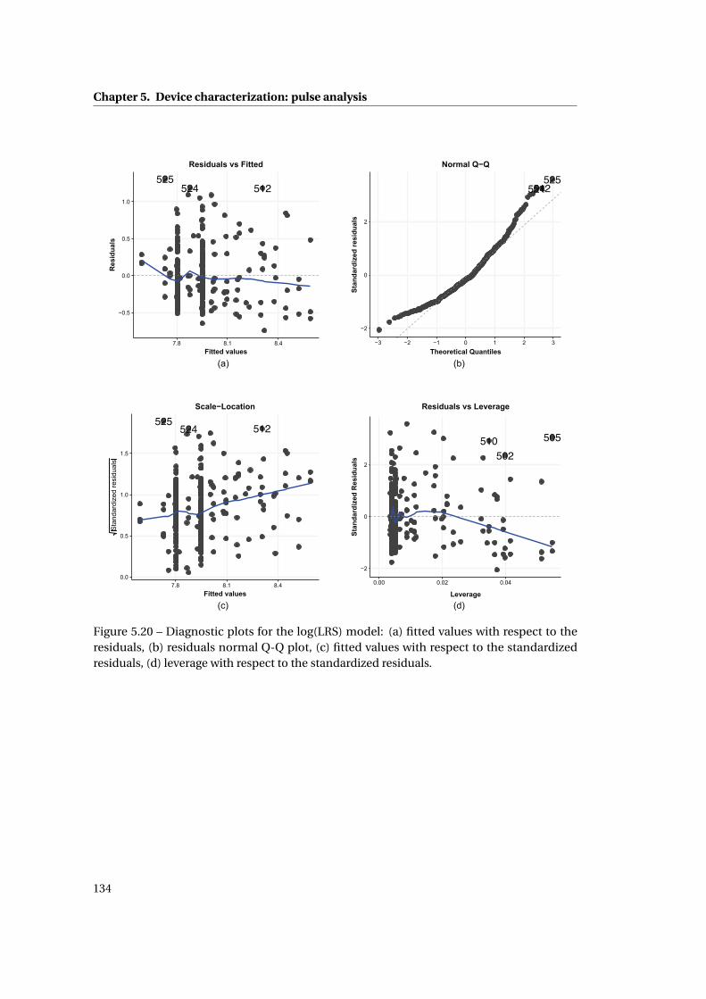
Chapter 5. Device characterization: pulse analysis
525524 512
525524512
525 524 512505510
502
Figure 5.20 – Diagnostic plots for the log(LRS) model: (a) fitted values with respect to theresiduals, (b) residuals normal Q-Q plot, (c) fitted values with respect to the standardizedresiduals, (d) leverage with respect to the standardized residuals.
134
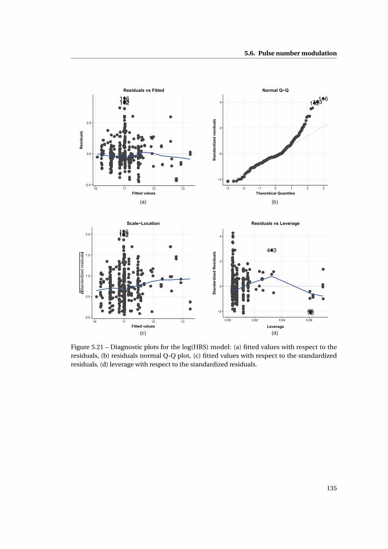
5.6. Pulse number modulation
116143142 116143142
116143142
70
443
69
Figure 5.21 – Diagnostic plots for the log(HRS) model: (a) fitted values with respect to theresiduals, (b) residuals normal Q-Q plot, (c) fitted values with respect to the standardizedresiduals, (d) leverage with respect to the standardized residuals.
135

Chapter 5. Device characterization: pulse analysis
pulses.
Fig. 5.22 (a) and Fig. 5.22 (b) show the result for subsequent reset pulses of −1.15 V and −1 V,
respectively. The reset pulses have 1μs width, 20% slope and a period of 100 ms (i.e., the time
between a pulse and the subsequent one, in case it is not followed by a read operation).
It is possible to draw several conclusions from the test results. First, the operating voltages
are lower than the normal reset pulse values used for the standard reset operations. As we
target a partial reset operation, the memory cell input pulse needs to be outside the input
validity domain: it should carry enough energy to induce a change, but not too much in order
to obtain just a gradual increase of the resistance, and not a unique switch to the HRS. Second,
the resistance value saturates after a certain number of pulses: once this value is reached,
the HRS varies around it. Third, the reset pulse voltage controls two key aspects of the tests:
the resistance saturation voltage and the maximum pulse number that induces a resistance
change. A very small reset pulse does not induce any change in the memory. On the contrary,
a large one (<−1.25 V) results in a large resistance change, but over a very short amount of
pulses. For example, if we apply a −1.25 V pulse, the resistance goes up to 100 kΩ after just one
pulse, and then it saturates at that value. The best results are obtained for moderate voltage
values (around −1 V), which allows obtaining a good resistance ratio over a relatively large
number of pulses. In the figure, −1.15 V pulse allows modulating the resistance over about 20
pulses, while a −1 V pulse allows modulating the resistance over 100 pulses. In both cases, the
resistance ratio is more than one decade. In summary, it appears to exist a trade-off between
the resistance saturation value and the number of pulses that induce a change in the memory,
which is highly influenced by the reset voltage.
Furthermore, it should be noticed that the resistance change is definitely non-linear, and
sometimes even not locally monotonic. We believe that the non-linearity comes from the
physical mechanisms behind the reset process, while the fluctuations are resulting from the
intrinsic stochasticity of the devices.
We did not attempt to extract a model to describe the resistance change with respect to the
number of pulses. These tests are meant to be a proof of concept, so they were not planned
in such a way to produce a complete database. Moreover, more characterizations should be
performed in order to assert the stability of the parameters and the variations in the resistance
results.
Finally, we did not try the same test procedure to induce a modulation of the LRS. As demon-
strated in the previous section, the control of the set process is much more complex, and it is
extremely dependent on the setup used. We believe that, regarding the LRS pulse modulation,
our setup does not allow the precision required to perform meaningful tests.
136
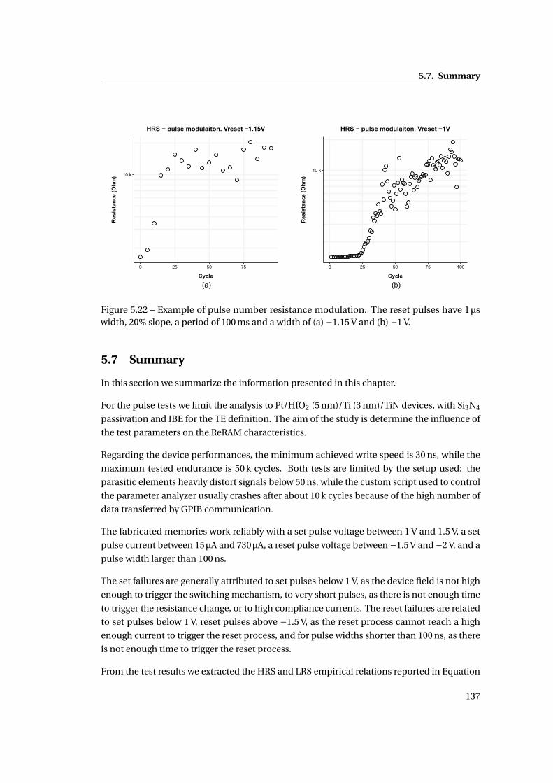
5.7. Summary
Figure 5.22 – Example of pulse number resistance modulation. The reset pulses have 1μswidth, 20% slope, a period of 100 ms and a width of (a) −1.15 V and (b) −1 V.
5.7 Summary
In this section we summarize the information presented in this chapter.
For the pulse tests we limit the analysis to Pt/HfO2 (5 nm)/Ti (3 nm)/TiN devices, with Si3N4
passivation and IBE for the TE definition. The aim of the study is determine the influence of
the test parameters on the ReRAM characteristics.
Regarding the device performances, the minimum achieved write speed is 30 ns, while the
maximum tested endurance is 50 k cycles. Both tests are limited by the setup used: the
parasitic elements heavily distort signals below 50 ns, while the custom script used to control
the parameter analyzer usually crashes after about 10 k cycles because of the high number of
data transferred by GPIB communication.
The fabricated memories work reliably with a set pulse voltage between 1 V and 1.5 V, a set
pulse current between 15μA and 730μA, a reset pulse voltage between −1.5 V and −2 V, and a
pulse width larger than 100 ns.
The set failures are generally attributed to set pulses below 1 V, as the device field is not high
enough to trigger the switching mechanism, to very short pulses, as there is not enough time
to trigger the resistance change, or to high compliance currents. The reset failures are related
to set pulses below 1 V, reset pulses above −1.5 V, as the reset process cannot reach a high
enough current to trigger the reset process, and for pulse widths shorter than 100 ns, as there
is not enough time to trigger the reset process.
From the test results we extracted the HRS and LRS empirical relations reported in Equation
137

Chapter 5. Device characterization: pulse analysis
5.1 and Equation 5.2:
Log (HRS) = 5.294–3.165×Vr eset +0.022× tpul se (5.1)
Log (LRS) = 12.369–1.462×Vset –1.364×Vg ate . (5.2)
The models show that the HRS is mainly controlled by the reset pulse voltage and the pulse
width. This is well explained if we consider that the reset is mainly a thermally assisted process.
On the contrary, the set pulse and the set compliance current do not influence the HRS as they
mainly play a role during the set process, while the pulse slope has no effect as it accounts for
a small change in time compared to the pulse width.
The LRS is mainly controlled by the set pulse voltage and the compliance current. This can be
explained considering that the set voltage is the parameter which triggers the set process, while
the compliance current is the main controller of the set phenomenon, as the maximum current
defines the width of the filament and the ReRAM final LRS resistance. On the contrary, the reset
pulse voltage and the pulse time do not influence the LRS. The reset pulse plays mostly a role
for the reset mechanism, while the pulse time does not influence the LRS as the phenomena
involved are much faster than the pulse width. Once the set process is triggered, the cell
current rises extremely fast due to a positive feedback, and the resulting atom configuration is
already quite stable. As a result, a longer of shorter pulse does not make a large difference.
The test results show that we can vary independently the LRS or the HRS for normal energy
regimes. If, on the contrary, we have a very large HRS or a small LRS, then we obtain an inverse
proportionality between the two resistance states. As noticed for the DC tests, a deep HRS
requires a large energy to overcome the high energy barrier between the states, and this results
in a poorly controlled LRS, which, as a consequence, usually shows a low resistance value.
Finally, we showed that is possible to operate the devices by modulating the number of write
operations. As a result, the resistance state shows an analogue behavior with a continuity
between the states.
138

6 CMOS system integration
This chapter describes the integration of the fabricated resistive memories within standard
CMOS technology. The intent is to obtain a hybrid ReRAM-CMOS system in a passive crossbar
array configuration. This chapter is divided as follows. First, in Section 6.1, we introduce the
main memory arrangements and the sneak-path current issue. Then, in Section 6.2, we show
a Verilog-A model used to simulate the device electrical behavior. Subsequently, in Section 6.3,
we present a CMOS read circuit implementation to reduce the sneak-current path in passive
crossbar memory arrays. In Section 6.4, we discuss the fabrication and characterization
of selector devices. Afterward, in Section 6.5, we show two methods to integrate resistive
memories in the back end of the line of CMOS chips. Finally, we conclude the chapter with a
summary of the work in Section 6.6.
6.1 Background
As mentioned in the ReRAM introduction chapter (Section 2.3), high-performance ReRAM
cells have been demonstrated with CMOS compatible materials [73] and low thermal budget
processes, making it possible to integrate the technology in the CMOS Back-End-of-Line
(BEoL). Few examples of such materials are TiN, used in CMOS technology as a barrier layer
for the metal lines, HfOx, used as high-κ dielectric for the CMOS gate oxide and TaOx, also
employed as an high-κ dielectric. Past demonstrations of ReRAM-CMOS integration mainly
came from CMOS foundries and were performed at wafer level [74, 75, 76, 77, 78]. The main
problems with this approach are a very low accessibility (just few fabs have hybrid ReRAM-
CMOS processes) and a high fabrication cost, because it requires a dedicated CMOS foundry.
Embedded ReRAMs are classically arranged in 1T1R, vertical 3D, passive 1R or 1S1R crossbar
configurations. In the 1T1R topology [79], each ReRAM cell is in series with a selector transistor,
which can optimally control the current flowing through the memory device. This configura-
tion is adopted for embedded applications in which the area is less a concern compared to the
performance.
139

Chapter 6. CMOS system integration
The vertical 3D topologies, like vertical ReRAMs (vReRAMs), enable a vertical stacking of the
memory layers [80]. The major drawback is the difficulty to integrate a selector device. The
film depositions need to be carefully optimized and it is challenging to use additional metals.
For these reasons the ReRAM cell usually requires, in this configuration, to be self-rectifying.
Finally, in a passive crossbar configuration, the top and bottom electrodes are directly con-
nected to the bit and word line of the memory array. In this case, the desired cell is selected by
activating the bit and word lines corresponding to the selected ReRAM cell. Two arrangements
are possible: 1R or 1S1R. In the first case, just the ReRAM element is in between the metal lines
[81], while for 1S1R the ReRAM is in series with a selector device. The passive crossbar config-
uration is desirable for storage class memory applications, where a trade-off of density and
performance is needed for applications in between DRAM and Flash. The major advantage of
this configuration is the small feature size (4F 2, where F is the lithography critical dimension)
and the possibility for stacking multiple memory layers.
Although the crossbar configuration is desirable for the above-mentioned reasons, it has
the inherent disadvantage of the presence of sneak-path current. The sneak-path current
originates from the leakage current of unselected devices in the LRS. This unwanted current,
proportional to the applied voltages and the size of the array, can compromise the read
operation.
Fig. 6.1 shows a schematic representation of the sneak-path current problem. In the example,
the current resulting from a read operation performed on the device in the HRS, reported in
blue in Fig. 6.1, is composed of two elements. The first one is the desired output current and
results from the voltage drop on the selected device, while the second term is the sneak-path
current. If the magnitude of this second term is comparable or larger than the one flowing
through the selected device, the circuit periphery may be led to an incorrect interpretation
of the addressed bit. The sneak-path current is dependent on the memory array size and
the resistance configuration of the cells. This leakage current is the major limitation for the
fabrication of large passive crossbar arrays. This limitation is even more severe in case we
consider in this analysis the CMOS technology variations.
The sneak-path current carries three negative effects for the system. First, it degrades the
sensing margin, which is defined as the difference of the outputs obtained for the LRS and
the HRS cells. The sensed current during the read operation is indeed influenced by the
sneak current. Second, sneak-path current imply an unwanted current consumption during
the write and read operations. The current flowing through the unselected cells in the LRS
increases the power consumption. Third, the sneak-current path effects make the system less
predictable, as they are related to the bit memory pattern.
Among the possible ways to target this problem, it is possible to mention the insertion of
proper selector devices [82], the use of special device configurations, like complementary
switching ReRAMs [83], and the design of dedicated read and write circuits [84].
140
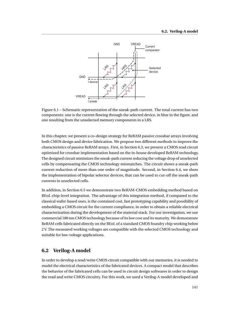
6.2. Verilog-A model
Figure 6.1 – Schematic representation of the sneak-path current. The total current has twocomponents: one is the current flowing through the selected device, in blue in the figure, andone resulting from the unselected memory components in a LRS.
In this chapter, we present a co-design strategy for ReRAM passive crossbar arrays involving
both CMOS design and device fabrication. We propose two different methods to improve the
characteristics of passive ReRAM arrays. First, in Section 6.3, we present a CMOS read circuit
optimized for crossbar implementation based on the in-house developed ReRAM technology.
The designed circuit minimizes the sneak-path current reducing the voltage drop of unselected
cells by compensating the CMOS technology mismatches. The circuit shows a sneak-path
current reduction of more than one order of magnitude. Second, in Section 6.4, we show
the implementation of bipolar selector devices, that can be used to cut-off the sneak-path
currents in unselected cells.
In addition, in Section 6.5 we demonstrate two ReRAM-CMOS embedding method based on
BEoL chip-level integration. The advantage of this integration method, if compared to the
classical wafer-based ones, is the contained cost, fast prototyping capability and possibility of
embedding a CMOS circuit for the current compliance, in order to obtain a reliable electrical
characterization during the development of the material stack. For our investigation, we use
commercial 180 nm CMOS technology because of its low cost and its maturity. We demonstrate
ReRAM cells fabricated directly on the BEoL of a standard CMOS foundry chip working below
2 V. The measured working voltages are compatible with the selected CMOS technology and
suitable for low-voltage applications.
6.2 Verilog-A model
In order to develop a read/write CMOS circuit compatible with our memories, it is needed to
model the electrical characteristics of the fabricated devices. A compact model that describes
the behavior of the fabricated cells can be used in circuit design softwares in order to design
the read and write CMOS circuitry. For this work, we used a Verilog-A model developed and
141
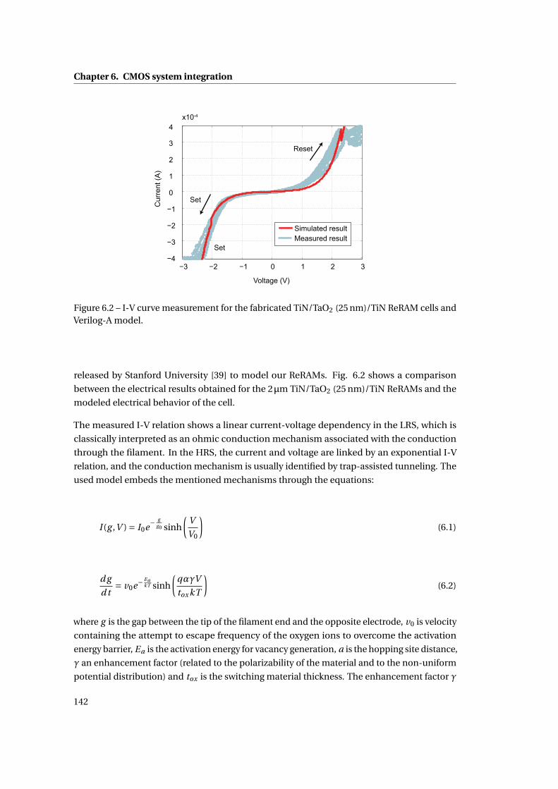
Chapter 6. CMOS system integration
Figure 6.2 – I-V curve measurement for the fabricated TiN/TaO2 (25 nm)/TiN ReRAM cells andVerilog-A model.
released by Stanford University [39] to model our ReRAMs. Fig. 6.2 shows a comparison
between the electrical results obtained for the 2μm TiN/TaO2 (25 nm)/TiN ReRAMs and the
modeled electrical behavior of the cell.
The measured I-V relation shows a linear current-voltage dependency in the LRS, which is
classically interpreted as an ohmic conduction mechanism associated with the conduction
through the filament. In the HRS, the current and voltage are linked by an exponential I-V
relation, and the conduction mechanism is usually identified by trap-assisted tunneling. The
used model embeds the mentioned mechanisms through the equations:
I (g ,V ) = I0e−g
g0 sinh
(V
V0
)(6.1)
d g
d t= v0e−
EakT sinh
(qαγV
tox kT
)(6.2)
where g is the gap between the tip of the filament end and the opposite electrode, v0 is velocity
containing the attempt to escape frequency of the oxygen ions to overcome the activation
energy barrier, Ea is the activation energy for vacancy generation, a is the hopping site distance,
γ an enhancement factor (related to the polarizability of the material and to the non-uniform
potential distribution) and tox is the switching material thickness. The enhancement factor γ
142

6.3. Circuit strategies for sneak-path current reduction
is calculated by the equation:
γ= γ0 −β
(g
10−9
)3
. (6.3)
Equation 6.1, which defines the current as an exponential function of the voltage and the
gap, describes both the linear and the exponential regimes of the ReRAM resistances. The
simulation results, shown in Fig. 6.2 together with the measured result, fit well the electrical
characteristic of the device, corroborating the hypothesis that the HRS I-V behavior is related
to tunneling-based phenomena. The fitting parameters used in the model are summarized in
Table 6.1. The Verilog-A model simulation is limited to −2.5 V because the cell current attains
the compliance value. In the simulation test bench there is no current limiter component, so
the maximum current flowing through the cell is limited by controlling the applied voltage.
This is possible in a simulation environment because of the deterministic behavior of the
model, while it is not suitable for electrical tests of real components due to the set voltage
variations. Furthermore, it is not possible to exactly simulate the cell behavior during the
reset process. This is due to the stochastic nature of the reset, which is caused by the random
probability associated to the filament breakdown phenomena.
Parameter name Value Unit Description
tox 20.55 nm Oxide thicknessgmax 455 pm Maximum gap valuegmi n 430 pm Maximum gap valueg0 125 pm Gap scaling factorV0 413.9 mV Voltage scaling factorv0 19 nm/ns Escape velocityI0 91.3 μA Current scaling factorβ 0.8 1 Gamma scaling factorγ0 16.2 1 Gamma initial valueδg 0 20 mm Random variations parameterFmi n 1.6 GV/m Minimum field for gap enhancement
Table 6.1 – Verilog-A model fitting parameters.
6.3 Circuit strategies for sneak-path current reduction
In order to limit the sneak-path current, we designed a read circuit that forces the potential
drop across the unselected devices to a value close to zero. This is obtained applying the same
voltage value at the device electrodes and compensating the technological mismatches with a
calibration circuit. This work has been reported in [85].
We designed the read/write circuit reported in Fig. 6.3. The system includes a digital controller,
143
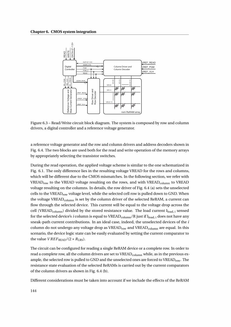
Chapter 6. CMOS system integration
Colume Driver and Column Decoder
Figure 6.3 – Read/Write circuit block diagram. The system is composed by row and columndrivers, a digital controller and a reference voltage generator.
a reference voltage generator and the row and column drivers and address decoders shown in
Fig. 6.4. The two blocks are used both for the read and write operation of the memory arrays
by appropriately selecting the transistor switches.
During the read operation, the applied voltage scheme is similar to the one schematized in
Fig. 6.1. The only difference lies in the resulting voltage VREAD for the rows and columns,
which will be different due to the CMOS mismatches. In the following section, we refer with
VREADrow to the VREAD voltage resulting on the rows, and with VREADcolumn to VREAD
voltage resulting on the columns. In details, the row driver of Fig. 6.4 (a) sets the unselected
cells to the VREADrow voltage level, while the selected cell row is pulled down to GND. When
the voltage VREADcolumn is set by the column driver of the selected ReRAM, a current can
flow through the selected device. This current will be equal to the voltage drop across the
cell (VREADcolumn) divided by the stored resistance value. The load current Iload, i sensed
for the selected device’s i column is equal to VREADcolumn/R just if Iload, i does not have any
sneak-path current contributions. In an ideal case, indeed, the unselected devices of the i
column do not undergo any voltage drop as VREADrow and VREADcolumn are equal. In this
scenario, the device logic state can be easily evaluated by setting the current comparator to
the value V REF READ/(2×RLRS).
The circuit can be configured for reading a single ReRAM device or a complete row. In order to
read a complete row, all the column drivers are set to VREADcolumn while, as in the previous ex-
ample, the selected row is pulled to GND and the unselected ones are forced to VREADrow. The
resistance state evaluation of the selected ReRAMs is carried out by the current comparators
of the column drivers as shown in Fig. 6.4 (b).
Different considerations must be taken into account if we include the effects of the ReRAM
144
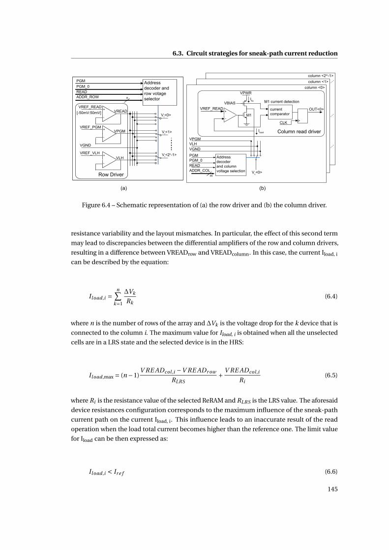
6.3. Circuit strategies for sneak-path current reduction
Figure 6.4 – Schematic representation of (a) the row driver and (b) the column driver.
resistance variability and the layout mismatches. In particular, the effect of this second term
may lead to discrepancies between the differential amplifiers of the row and column drivers,
resulting in a difference between VREADrow and VREADcolumn. In this case, the current Iload, i
can be described by the equation:
Iload ,i =n∑
k=1
ΔVk
Rk(6.4)
where n is the number of rows of the array and ΔVk is the voltage drop for the k device that is
connected to the column i. The maximum value for Iload, i is obtained when all the unselected
cells are in a LRS state and the selected device is in the HRS:
Iload ,max = (n −1)V RE ADcol ,i −V RE ADr ow
RLRS+ V RE ADcol ,i
Ri(6.5)
where Ri is the resistance value of the selected ReRAM and RLRS is the LRS value. The aforesaid
device resistances configuration corresponds to the maximum influence of the sneak-path
current path on the current Iload, i. This influence leads to an inaccurate result of the read
operation when the load total current becomes higher than the reference one. The limit value
for Iload can be then expressed as:
Iload ,i < Ir e f (6.6)
145
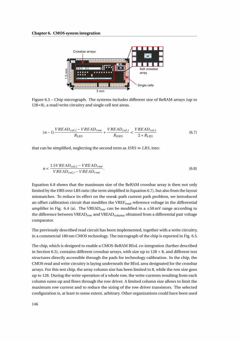
Chapter 6. CMOS system integration
Figure 6.5 – Chip micrograph. The systems includes different size of ReRAM arrays (up to128×8), a read/write circuitry and single cell test areas.
(n −1)V RE ADcol ,i −V RE ADr ow
RLRS+ V RE ADcol ,i
RHRS< V RE ADcol ,i
2×RLRS(6.7)
that can be simplified, neglecting the second term as HRS � LRS, into:
n < 1.5V RE ADcol ,i −V RE ADr ow
V RE ADcol ,i −V RE ADr ow. (6.8)
Equation 6.8 shows that the maximum size of the ReRAM crossbar array is then not only
limited by the HRS over LRS ratio (the term simplified in Equation 6.7), but also from the layout
mismatches. To reduce its effect on the sneak-path current path problem, we introduced
an offset calibration circuit that modifies the VREFread reference voltage in the differential
amplifier in Fig. 6.4 (a). The VREADrow can be modified in a ±50 mV range according to
the difference between VREADrow and VREADcolumn obtained from a differential pair voltage
comparator.
The previously described read circuit has been implemented, together with a write circuitry,
in a commercial 180 nm CMOS technology. The micrograph of the chip is reported in Fig. 6.5.
The chip, which is designed to enable a CMOS-ReRAM BEoL co-integration (further described
in Section 6.5), contains different crossbar arrays, with size up to 128 × 8, and different test
structures directly accessible through the pads for technology calibration. In the chip, the
CMOS read and write circuitry is laying underneath the BEoL area designated for the crossbar
arrays. For this test chip, the array column size has been limited to 8, while the row size goes
up to 128. During the write operation of a whole row, the write currents resulting from each
column sums up and flows through the row driver. A limited column size allows to limit the
maximum row current and to reduce the sizing of the row driver transistors. The selected
configuration is, at least to some extent, arbitrary. Other organizations could have been used
146
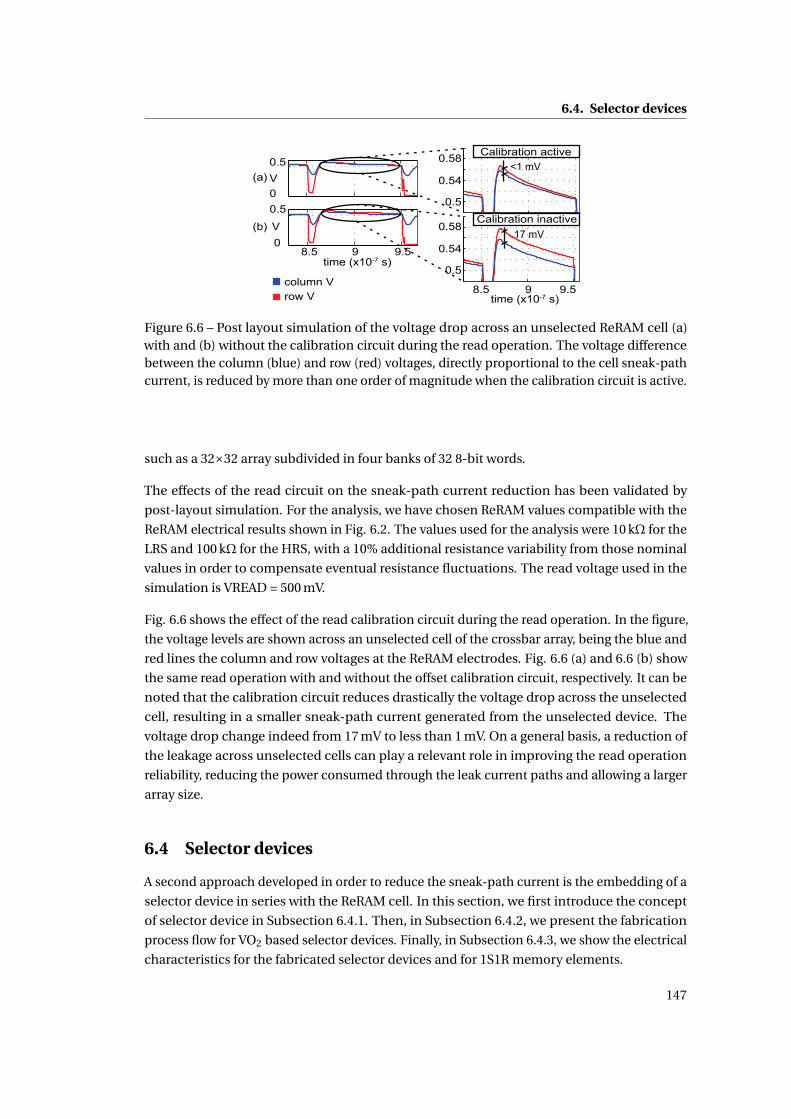
6.4. Selector devices
Figure 6.6 – Post layout simulation of the voltage drop across an unselected ReRAM cell (a)with and (b) without the calibration circuit during the read operation. The voltage differencebetween the column (blue) and row (red) voltages, directly proportional to the cell sneak-pathcurrent, is reduced by more than one order of magnitude when the calibration circuit is active.
such as a 32×32 array subdivided in four banks of 32 8-bit words.
The effects of the read circuit on the sneak-path current reduction has been validated by
post-layout simulation. For the analysis, we have chosen ReRAM values compatible with the
ReRAM electrical results shown in Fig. 6.2. The values used for the analysis were 10 kΩ for the
LRS and 100 kΩ for the HRS, with a 10% additional resistance variability from those nominal
values in order to compensate eventual resistance fluctuations. The read voltage used in the
simulation is VREAD = 500 mV.
Fig. 6.6 shows the effect of the read calibration circuit during the read operation. In the figure,
the voltage levels are shown across an unselected cell of the crossbar array, being the blue and
red lines the column and row voltages at the ReRAM electrodes. Fig. 6.6 (a) and 6.6 (b) show
the same read operation with and without the offset calibration circuit, respectively. It can be
noted that the calibration circuit reduces drastically the voltage drop across the unselected
cell, resulting in a smaller sneak-path current generated from the unselected device. The
voltage drop change indeed from 17 mV to less than 1 mV. On a general basis, a reduction of
the leakage across unselected cells can play a relevant role in improving the read operation
reliability, reducing the power consumed through the leak current paths and allowing a larger
array size.
6.4 Selector devices
A second approach developed in order to reduce the sneak-path current is the embedding of a
selector device in series with the ReRAM cell. In this section, we first introduce the concept
of selector device in Subsection 6.4.1. Then, in Subsection 6.4.2, we present the fabrication
process flow for VO2 based selector devices. Finally, in Subsection 6.4.3, we show the electrical
characteristics for the fabricated selector devices and for 1S1R memory elements.
147
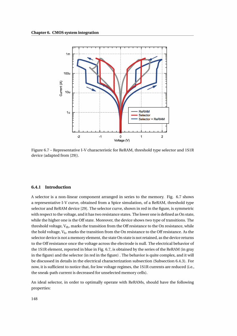
Chapter 6. CMOS system integration
Figure 6.7 – Representative I-V characteristic for ReRAM, threshold type selector and 1S1Rdevice (adapted from [29]).
6.4.1 Introduction
A selector is a non-linear component arranged in series to the memory. Fig. 6.7 shows
a representative I-V curve, obtained from a Spice simulation, of a ReRAM, threshold type
selector and ReRAM device [29]. The selector curve, shown in red in the figure, is symmetric
with respect to the voltage, and it has two resistance states. The lower one is defined as On state,
while the higher one is the Off state. Moreover, the device shows two type of transitions. The
threshold voltage, Vth, marks the transition from the Off resistance to the On resistance, while
the hold voltage, Vh, marks the transition from the On resistance to the Off resistance. As the
selector device is not a memory element, the state On state is not retained, as the device returns
to the Off resistance once the voltage across the electrode is null. The electrical behavior of
the 1S1R element, reported in blue in Fig. 6.7, is obtained by the series of the ReRAM (in gray
in the figure) and the selector (in red in the figure) . The behavior is quite complex, and it will
be discussed in details in the electrical characterization subsection (Subsection 6.4.3). For
now, it is sufficient to notice that, for low voltage regimes, the 1S1R currents are reduced (i.e.,
the sneak-path current is decreased for unselected memory cells).
An ideal selector, in order to optimally operate with ReRAMs, should have the following
properties:
148
6.4. Selector devices
Ion current density. The selector device should carry a high enough current density in order
to ensure the reset operation. For highly scaled devices (∼10 nm), supposing a 10μA reset
current, the current density should be higher than 10 MA/cm2. It is important to underline
that the ReRAM writing current does not scale with the device area, which may eventually
limit the memory scaling. These current values are close to the maximum current delivered by
a 10 nm Cu wire, which is 2μA (due to electromigration effects, calculated for a 10 years life
time [86]).
On-Off ratio or rectification ratio. Selector devices need to have large enough difference in
the conductive-state and blocking-state resistances. The parameter known as On-Off ratio
(e.g., for switch-based selector devices) or rectification ratio (e.g., for diode-based selector
devices) defines this difference. The On-Off ratio is an important factor to determine the size
of the memory array. Although this relation depends by many other factors (e.g., the resistance
of the metal lines, the minimum read margin, the ReRAM resistance values . . . ), a reference
value for the On-Off ratio is 105 for a one Gb array [82]. It is important to notice that the On-Off
ratio varies with the measurement voltage, so the ratio needs to be defined at appropriate
forward and reverse voltages.
Scalability. Selector devices should have similar scalability as the memory element, other-
wise the scaling advantage of emerging memories and crossbar arrays may be compromised
by selector devices. ReRAM functionality has been demonstrated down to 10 nm [10]. Today,
it appears that selector device represents a challenge for memory scaling down to 10 nm and
below.
Threshold voltage. It is defined as the turn-on voltage of the selector. It affects the effective
voltage passed to the memory elements. A target value is ∼1 V.
Other properties. Other properties should be the possibility of allowing bipolar operations,
high switching speed, endurance comparable to ReRAMs, manufacturability (compatible
processing temperature and materials) and low device variability.
In the literature, several devices have been proposed as selectors. Hereafter we present a short
survey of the main alternatives.
Transistor. So far transistors have been a natural choice for selector devices. Flash memory
is a good example of a memory element (charge storage in the floating gate) and a selector
device (transistor) combined in one device. The most reported ReRAM test chips use 1T1R
configuration where an access transistor is connected in series with a two-terminal memory
element to provide both device selection and switching control functions. The transistor Vg
149

Chapter 6. CMOS system integration
controls the current supplied to the memory element during the switching process, which
has been shown to play critical roles in the switching properties of ReRAM. Transistor charac-
teristics and their scaling trend are well understood, therefore their compatibility for future
generation memories can be better projected than other less mature selector devices.
The major disadvantages of transistors as selector devices are the >4F2 footprint of planar
transistors and the high processing temperature that limits transistors in stackable memories.
Due to these challenges associated with transistors as the selector device, 1T1R does not
appear competitive against 3D NAND. The role of transistors can be changed from a selector
device for each memory element inside of an array to an access device in the peripheral to a
block of small crossbar array. The peripheral transistors will control the access to the block
and limit the voltage/current during operation. The memory elements inside of the array can
be connected to two-terminal nonlinear devices. Since peripheral transistors do not need
to scale as aggressively as the memory element and can be made much bigger, transistor
resistance is less a problem.
Si diode. Diodes as selector devices have advantages, with respect to transistors, in scalability
and simplicity. The major challenge of Si diode is the high processing temperature required to
crystallize Si to reduce contact resistivity and off-current. This limits the use of single-crystal
Si diode as selector devices in multi-layer memory arrays. Recent results of Si diodes has
demonstrated scalability down to 20 nm [87]. A further scaling of diodes is problematic due to
doping fluctuations. As an example, a 10 nm×10 nm×10 nm diode with a doping concentration
of 1018 will result in a single dopant atoms (this intermediate doping concentration is needed
in ’standard’ diodes to avoid a low breakdown voltage). Therefore, for highly scaled diodes,
doping fluctuation may be a serious issue. Another issue is the contact resistance: a resistivity
of 10-6 Ω/cm2, with a device size of 10 nm2, will result in a 1 MΩ contact. The voltage drop on
such a large resistance will result in a 1 V drop with a current of 1μA. Moreover, in order to
ensure bipolar characteristics, diodes needs to allow high enough current in the off-state to
allow the cell switching.
Poly Si diode. Using poly Si diodes may enable stackable memory layer above peripheral
circuits built on Si wafers. An On-Off ratio of 108 has been demonstrated in poly Si diodes,
with a Jon of 10 MA at 2 V [88]. A poly Si diode has the same disadvantages as the Si diodes,
but, in general, in poly Si diodes it is more difficult to control the junction diffusion. Another
disadvantage is the variability in polycrystalline scaled devices with respect to the grain size.
The most significant problem of Si diode is the rather high process temperature. Silicon should
be crystallized to reduce resistivity and off current density.
Oxide diode. Oxide diode materials are interesting for low-temperature processing of se-
lector devices. However, these diodes are not yet able to provide the same level of switching
150
6.4. Selector devices
current and On-Off ratio as Si diodes. Oxide diode performance is mainly determined by
carrier density (defect related) and mobility, which are usually both lower than these in Si.
Therefore, oxide diodes are probably not going to be better than Si diodes. In addition, the con-
tact resistance of oxide diodes may be worse. Moreover, the Off current should be high enough
in order to ensure ReRAM bipolar characteristics. The forward current can be increased by
reducing the band gap of the materials. A Jon current of 0.1 MA has been demonstrated with
CuO/InZnO junctions [89].Their advantages are on low processing temperature and suitability
for stackable structures.
Symmetric oxide Schottky diodes. Symmetric metal-oxide Schottky diodes consist of two
adjacent Schottky barriers. This has been demonstrated with materials such as Ni/TiO2/Ni.
The device shows an On-Off ratio of 103 and good area scaling. The On current (0.1 MA/cm2)
can be increased by reducing the barrier height [82]. Similar results have been shown with
TaN/SiNx/TaN [90]. In general a Schottky diode, compared to a p-n diode, has the following
characteristics: it is faster, as there is no need to extract the minority carriers, it has an ideality
factor close to 1, as there is no recombination in the depletion region (for p-n diodes this
value is around two), and it has a higher leakage current, as the thermionic prefactor is ∼107,
around 103 times more than the p-n diode one. Moreover, it has a lower turn-on voltage (0.3 V
compared to 0.7 V), it is less sensitive to the temperature, as the temperature affects principally
the minority carriers, and, finally, it is more difficult to fabricate, as it is critical to obtain a
good interface with no defects.
Metal-insulator Transition. Metal-Insulator Transition (MIT) is an thermal-electronic effect
that switch the resistance of the device. A well-known MIT material is VOx. Pt/VO2/Pt selector
devices have been demonstrated with on-current densities of 106 A/cm2, with a Vth of 0.35 V
and with an on-off ratio of 50 [91]. VO2 has a transition temperature of 67° C, which can be
problematic in CMOS circuits for certain applications. Nevertheless, this temperature can be
increased by doping the MIT material. Others materials that show MIT properties are NbOx
and NiOx.
Mixed Ionic Electronic Conduction. Mixed Ionic Electronic Conduction (MIEC) is a selector
developed by IBM. Its exact composition is undisclosed. The only information available is that
it is composed of a metal-insulator-metal structure with a Cu-based inter-layer. The layer is in
between a top electrode (e.g., TiN, W) and a bottom electrode. The demonstrated electrical
characteristics are an On-Off ratio of 107, a maximum On current of 50 MA/cm2, a Vth of 0.75 V,
scalability to 28 nm and good endurance [92].
Ovonic Threshold Switch. Ovonic Threshold Switch (OTS) refers to the reversible threshold
switching of amorphous chalcogenide materials. OTS is interesting because Ron does not
151
Chapter 6. CMOS system integration
follow the simple Ohm’s law. In other words, it does not linearly decrease with 1/A while Roff
does. Instead, the dependence of Ron is described by 1/w, rather than 1/A, where w is the
width of the top or bottom electrode. This property makes OTS appealing for the property of
conducting a high current also at small technological nodes [93]. The On current of Ge/Se-
based OTS devices is estimated to be over 0.3 MA/cm2. However, the threshold voltage (Vth) is
observed to increase with the decrease of the device thickness laying challenges to be resolved.
Standard values for the Vth in Ge/Se materials are around 2 V.
For this work, we decided to focus on MIT material-based selectors as they are bipolar, they
can carry a large current density and they are relatively easy to fabricate. In the following
subsection we describe the fabrication process (Subsection 6.4.2) and the electrical results
(Subsection 6.4.3) for VO2-based selector devices. Moreover, we also show the results for a
1S1R configuration with the selector device and our ReRAM memories (Subsection 6.4.3).
The aim of this experiment is to fabricate a working 1S1R prototype, and to show the effective
reduction of the sneak-path current for unselected devices. Unfortunately, due to the timing
constraints of this work, there was not enough time to further develop and improve the selector
characteristics. In the literature, the use of VO2-based selector devices has been previously
reported in [91, 94].
6.4.2 Fabrication
As the process for the selector fabrication has not been previously optimized, we decided to
take a conservative approach by using the shadow mask process (Section 3.6), i.e., by avoiding
the VO2 etching. This allowed a simplification of the fabrication steps, and, as we used a
process previously developed for ReRAMs, it will help a future integration of 1S1R structures
on the same substrate. Moreover, we deposited a relatively thick VO2 film at high temperature.
This ensures a good crystallinity level in the VO2 film, and reduces the risk of failure of the
selector device. Eventual optimization of the process flow, such as the VO2 etching recipe and
the use of thinner films at lower deposition temperatures, can be further developed in future
studies. As mentioned before, this is an exploratory process run to determine the feasibility of
the process and the general electrical characteristics of the obtained devices.
The device fabrication is carried on with the shadow mask-based process described in Section
3.6. The substrates have Pt BE and SiO2 passivation, and the MIT material is patterned by
means of a shadow mask, as well as the TE.
The VO2 deposition is performed in the framework of a collaboration with the Solar Energy
and Building Physics Laboratory (LESO-PB) of EPFL. The material is deposited by reactive
magnetron sputtering in a custom-made machine from a V target after the chamber is pumped
down to 8×10⁻⁸ mbar. The substrate is annealed at a heating rate of 30° C/min up to 600° C
and kept at a constant temperature during the deposition. The deposition is performed in
an Ar plasma (12.5 sccm, 2×10⁻³ mbar) at 150 W. The O flow, set to 2.40 sccm, is monitored
152
6.4. Selector devices
by a lambda probe and adjusted by a PID controller. The deposition time is 2 h, which
results in a 300 nm thick film, and the substrate is brought back to room temperature at a
cooling rate of 30° C/min. During our fabrication run, unfortunately, while starting the VO2
deposition, a power glitch shut off the heater, which was not able to maintain the selected
temperature during the deposition. In order to ensure the film crystallization, we added a 1 h
post deposition bake at 500° C.
The process finishes with the deposition of the Pt TE by sputtering, as described for the shadow
mask-based process in Section 3.6.
6.4.3 Electrical characterization
The Pt/VO2/Pt selector devices are tested in DC with the same setup used for the ReRAMs. A
summary of the test results for the 2μm VIA selectors is shown in Fig. 6.8. Fig. 6.8 (a) reports
the I-V curve for 50 cycles on the same device. The results show a Vth and Vh of 1.42 V and
0.26 V, respectively. The resistance states, measured at 0.9 V and 0.45 V, are 89Ω and 1.2 kΩ.
Moreover, the device shows perfectly symmetric characteristics for positive and negative
actuation voltages. This is extremely interesting, as it allows to operate bipolar memories, such
as ReRAMs. The On and Off resistance state distribution is reported in Fig. 6.8 (b). From the
figure, it is possible to notice that the resistance variability is quite low both for different cycles
and different devices. It should be highlighted that the On resistance value results "pinned"
because it is measured by a script at the current compliance (0.9 V). The actual resistance
is probably below the number reported in the graph. Fig. 6.8 (c) show the threshold and
hold voltages for the measured samples. In this case, the device-to-device variability is more
important, while the cycle-to-cycle changes are quite small. It must be highlighted that for
MIT devices the variable that induces the state transitions is the current, and not the voltage.
This means that both the threshold and the hold transitions are triggered from a current. This
happens because the state transition is generated by thermal effect, and not field effect. For
our devices, the threshold transition is at 2 mA, while the hold transition is at 5 mA.
These device electrical properties may be adjusted by properly engineering the MIT material,
as from the literature it is suggested that the atomic radius of the dopant is determinant in
this context [95]. For instance, it might be possible to modify the transition temperature by
doping it with Al3+, Ga3+, Ge3+, Fe3+ and Cr3+, as these ions behave as acceptors in VO2 and
they may raise the transition temperature [96]. On the contrary, ions such as W6+, Ru4+, Nb5+,
Ta5+, Mo6+ mostly behave as donors in VO2 and they may lower the transition temperature
[97].
The electrical results for the 1S1R configuration with the Pt/VO2/Pt selector and the Pt/HfO2
(5 nm)/Ti (3 nm)/TiN ReRAM are shown in Fig. 6.9. In this proof of concept, the memory
and the selector are physically wired to each other, so they are not integrated on the same
substrate. For the image it is possible to notice that the stack electrical behavior is quite
complex. Starting from 0 V, the two devices are in the high resistive state. The ReRAM device
153
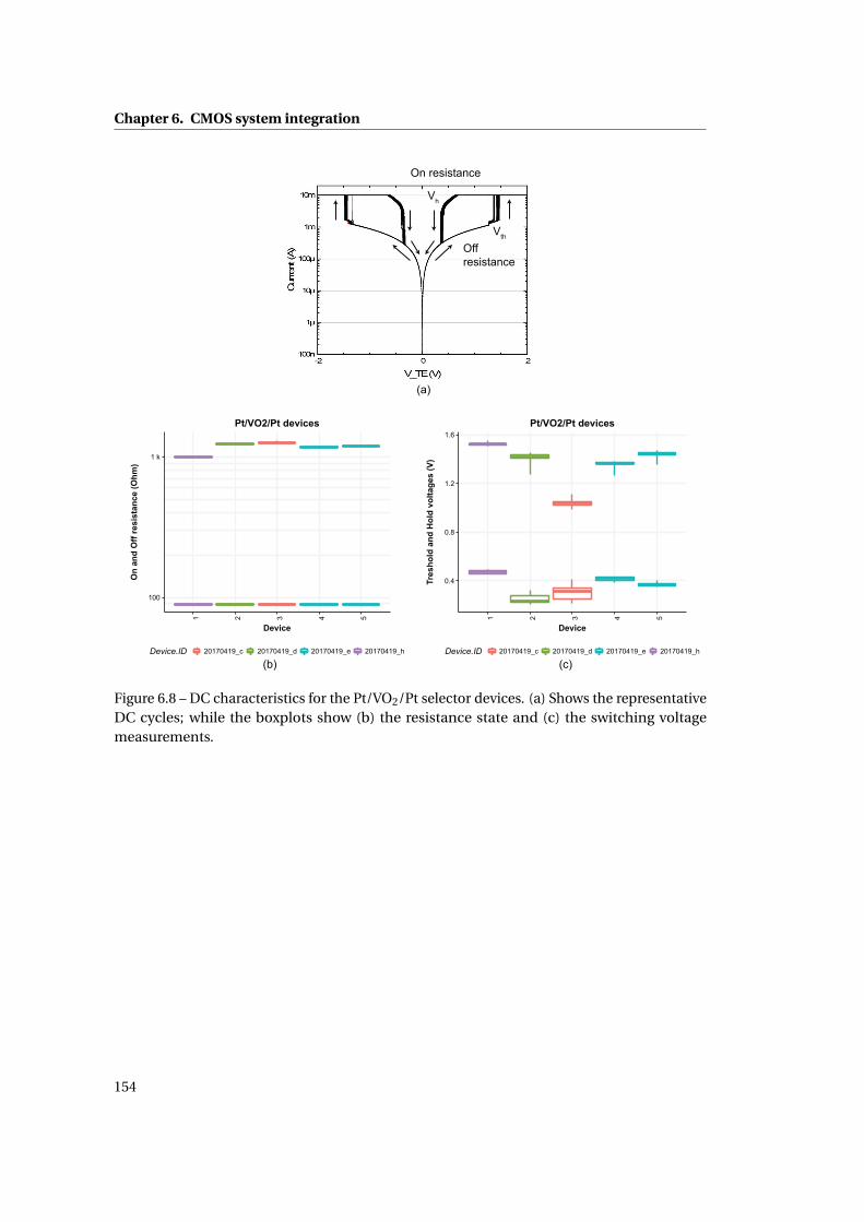
Chapter 6. CMOS system integration
Figure 6.8 – DC characteristics for the Pt/VO2/Pt selector devices. (a) Shows the representativeDC cycles; while the boxplots show (b) the resistance state and (c) the switching voltagemeasurements.
154
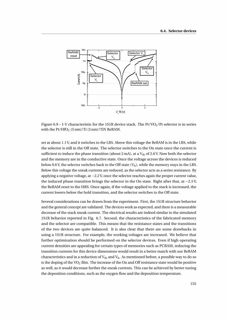
6.4. Selector devices
Figure 6.9 – I-V characteristic for the 1S1R device stack. The Pt/VO2/Pt selector is in serieswith the Pt/HfO2 (5 nm)/Ti (3 nm)/TiN ReRAM.
set at about 1.1 V, and it switches to the LRS. Above this voltage the ReRAM is in the LRS, while
the selector is still in the Off state. The selector switches to the On state once the current is
sufficient to induce the phase transition (about 2 mA), at a Vth of 2.6 V. Now both the selector
and the memory are in the conductive state. Once the voltage across the devices is reduced
below 0.6 V, the selector switches back to the Off state (Vh), while the memory stays in the LRS.
Below this voltage the sneak currents are reduced, as the selector acts as a series resistance. By
applying a negative voltage, at −2.2 V, once the selector reaches again the proper current value,
the induced phase transition brings the selector in the On state. Right after that, at −2.5 V,
the ReRAM reset to the HRS. Once again, if the voltage applied to the stack is increased, the
current lowers below the hold transition, and the selector switches to the Off state.
Several considerations can be drawn from the experiment. First, the 1S1R structure behavior
and the general concept are validated. The devices work as expected, and there is a measurable
decrease of the stack sneak current. The electrical results are indeed similar to the simulated
1S1R behavior reported in Fig. 6.7. Second, the characteristics of the fabricated memory
and the selector are compatible. This means that the resistance states and the transitions
of the two devices are quite balanced. It is also clear that there are some drawbacks in
using a 1S1R structure. For example, the working voltages are increased. We believe that
further optimization should be performed on the selector devices. Even if high operating
current densities are appealing for certain types of memories such as PCRAM, reducing the
transition currents for this device dimensions would result in a better match with our ReRAM
characteristics and in a reduction of Vth and Vh. As mentioned before, a possible way to do so
is the doping of the VO2 film. The increase of the On and Off resistance state would be positive
as well, as it would decrease further the sneak currents. This can be achieved by better tuning
the deposition conditions, such as the oxygen flow and the deposition temperature.
155

Chapter 6. CMOS system integration
Figure 6.10 – (a) Scanning electron micrograph of the MMC capacitor and (b) FIB-SEM crosssection.
6.5 ReRAM chip-level integration
In this section, two methods to integrate ReRAM on the BEoL of fully finished 180 nm CMOS
foundry chip are presented. As mentioned before, the ability to achieve chip level ReRAM co-
integration is a key factor in order to lower fabrication costs and to speed up the prototyping
ability. The main challenges of this methodology, rather than working at the wafer-level, are the
chip handling and the lithography steps. The solution adopted to overcome these difficulties
is the embedding of the CMOS chip in a carrier wafer. A wafer carrier helps indeed with
the chip handling, enabling the use of machines that are designed to operate with standard
Si wafers, and helps the lithography process, permitting the use of standard Cr-glass masks.
Subsequently to the chip embedding, the die is processed to integrate the ReRAM memories on
the CMOS chip. The two proposed integration methods, based on a metal-to-metal capacitor
and top-metal integration, are discussed in the following subsections.
6.5.1 MMC-based approach
The first integration technique, reported by our group in [98, 99, 100], is based on a feature
called Metal to Metal Capacitor (MMC), which is commonly used in standard CMOS technol-
ogy to create small embedded capacitors.
A scanning electron micrograph of a MMC structure is reported in Fig. 6.10. The MMC layer,
in blue in the picture, is electrically connected to the Metal 6 (M6) by means of internal VIA,
and insulated from the Metal 5 (M5) by a 50 nm thick dielectric layer. The structure acts as a
capacitor with the MMC layer and M5 being the top and bottom electrode, respectively.
In the following text, we present the integration process flow and the electrical results for the
MMC-based integration approach.
Integration process flow
The developed process flow to create the carrier wafer is summarized in Fig. 6.11. The
carrier wafer is fabricated starting from a standard 4-inch Si wafer [Fig. 6.11 (a)]. After a
156
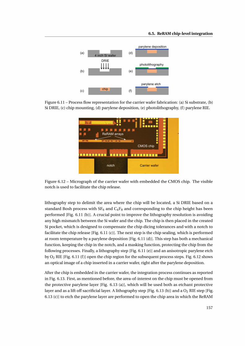
6.5. ReRAM chip-level integration
Figure 6.11 – Process flow representation for the carrier wafer fabrication: (a) Si substrate, (b)Si DRIE, (c) chip mounting, (d) parylene deposition, (e) photolithography, (f) parylene RIE.
Figure 6.12 – Micrograph of the carrier wafer with embedded the CMOS chip. The visiblenotch is used to facilitate the chip release.
lithography step to delimit the area where the chip will be located, a Si DRIE based on a
standard Bosh process with SF6 and C4F8 and corresponding to the chip height has been
performed [Fig. 6.11 (b)]. A crucial point to improve the lithography resolution is avoiding
any high mismatch between the Si wafer and the chip. The chip is then placed in the created
Si pocket, which is designed to compensate the chip dicing tolerances and with a notch to
facilitate the chip release [Fig. 6.11 (c)]. The next step is the chip sealing, which is performed
at room temperature by a parylene deposition [Fig. 6.11 (d)]. This step has both a mechanical
function, keeping the chip in the notch, and a masking function, protecting the chip from the
following processes. Finally, a lithography step [Fig. 6.11 (e)] and an anisotropic parylene etch
by O2 RIE [Fig. 6.11 (f)] open the chip region for the subsequent process steps. Fig. 6.12 shows
an optical image of a chip inserted in a carrier wafer, right after the parylene deposition.
After the chip is embedded in the carrier wafer, the integration process continues as reported
in Fig. 6.13. First, as mentioned before, the area-of-interest on the chip must be opened from
the protective parylene layer [Fig. 6.13 (a)], which will be used both as etchant protective
layer and as a lift off sacrificial layer. A lithography step [Fig. 6.13 (b)] and a O2 RIE step [Fig.
6.13 (c)] to etch the parylene layer are performed to open the chip area in which the ReRAM
157
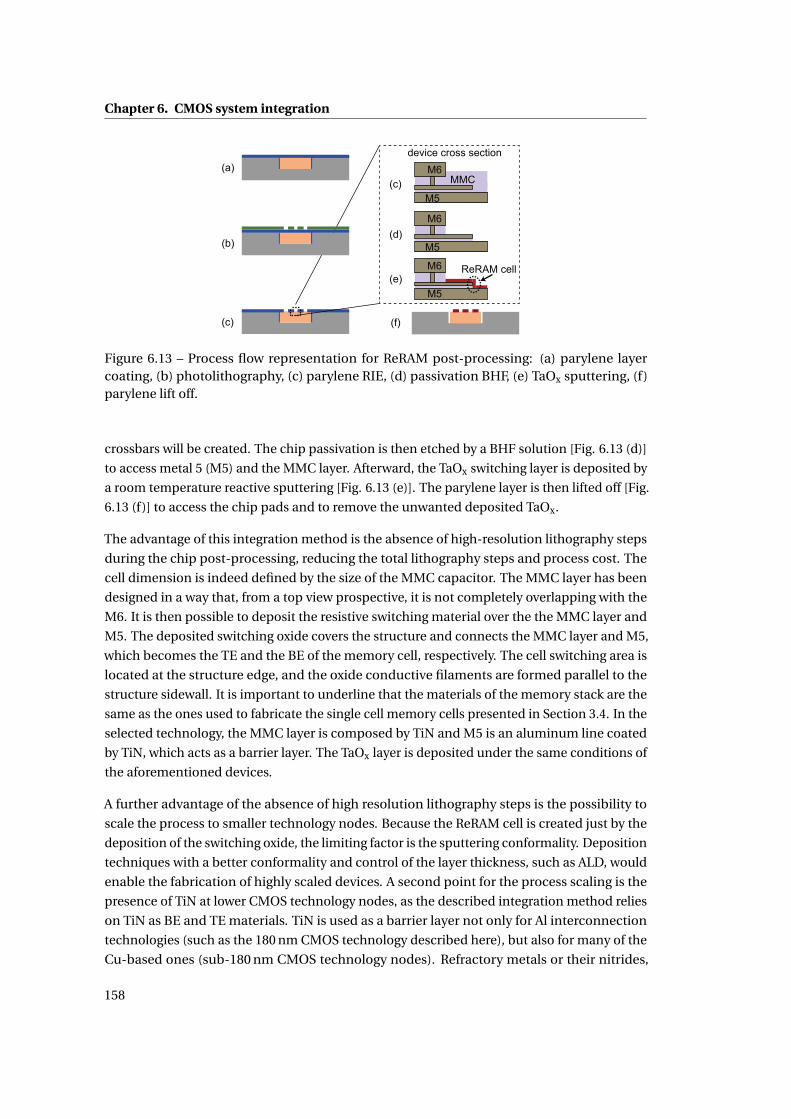
Chapter 6. CMOS system integration
Figure 6.13 – Process flow representation for ReRAM post-processing: (a) parylene layercoating, (b) photolithography, (c) parylene RIE, (d) passivation BHF, (e) TaOx sputtering, (f)parylene lift off.
crossbars will be created. The chip passivation is then etched by a BHF solution [Fig. 6.13 (d)]
to access metal 5 (M5) and the MMC layer. Afterward, the TaOx switching layer is deposited by
a room temperature reactive sputtering [Fig. 6.13 (e)]. The parylene layer is then lifted off [Fig.
6.13 (f)] to access the chip pads and to remove the unwanted deposited TaOx.
The advantage of this integration method is the absence of high-resolution lithography steps
during the chip post-processing, reducing the total lithography steps and process cost. The
cell dimension is indeed defined by the size of the MMC capacitor. The MMC layer has been
designed in a way that, from a top view prospective, it is not completely overlapping with the
M6. It is then possible to deposit the resistive switching material over the the MMC layer and
M5. The deposited switching oxide covers the structure and connects the MMC layer and M5,
which becomes the TE and the BE of the memory cell, respectively. The cell switching area is
located at the structure edge, and the oxide conductive filaments are formed parallel to the
structure sidewall. It is important to underline that the materials of the memory stack are the
same as the ones used to fabricate the single cell memory cells presented in Section 3.4. In the
selected technology, the MMC layer is composed by TiN and M5 is an aluminum line coated
by TiN, which acts as a barrier layer. The TaOx layer is deposited under the same conditions of
the aforementioned devices.
A further advantage of the absence of high resolution lithography steps is the possibility to
scale the process to smaller technology nodes. Because the ReRAM cell is created just by the
deposition of the switching oxide, the limiting factor is the sputtering conformality. Deposition
techniques with a better conformality and control of the layer thickness, such as ALD, would
enable the fabrication of highly scaled devices. A second point for the process scaling is the
presence of TiN at lower CMOS technology nodes, as the described integration method relies
on TiN as BE and TE materials. TiN is used as a barrier layer not only for Al interconnection
technologies (such as the 180 nm CMOS technology described here), but also for many of the
Cu-based ones (sub-180 nm CMOS technology nodes). Refractory metals or their nitrides,
158
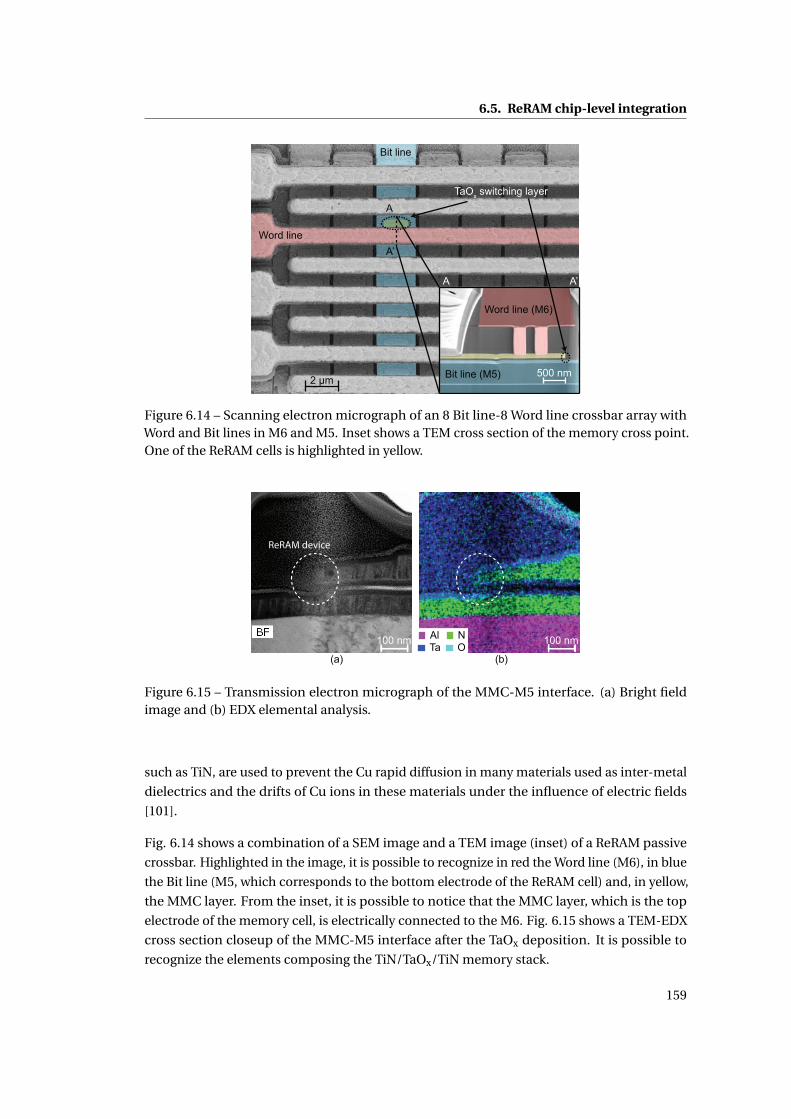
6.5. ReRAM chip-level integration
Figure 6.14 – Scanning electron micrograph of an 8 Bit line-8 Word line crossbar array withWord and Bit lines in M6 and M5. Inset shows a TEM cross section of the memory cross point.One of the ReRAM cells is highlighted in yellow.
ReRAM device
Figure 6.15 – Transmission electron micrograph of the MMC-M5 interface. (a) Bright fieldimage and (b) EDX elemental analysis.
such as TiN, are used to prevent the Cu rapid diffusion in many materials used as inter-metal
dielectrics and the drifts of Cu ions in these materials under the influence of electric fields
[101].
Fig. 6.14 shows a combination of a SEM image and a TEM image (inset) of a ReRAM passive
crossbar. Highlighted in the image, it is possible to recognize in red the Word line (M6), in blue
the Bit line (M5, which corresponds to the bottom electrode of the ReRAM cell) and, in yellow,
the MMC layer. From the inset, it is possible to notice that the MMC layer, which is the top
electrode of the memory cell, is electrically connected to the M6. Fig. 6.15 shows a TEM-EDX
cross section closeup of the MMC-M5 interface after the TaOx deposition. It is possible to
recognize the elements composing the TiN/TaOx/TiN memory stack.
159
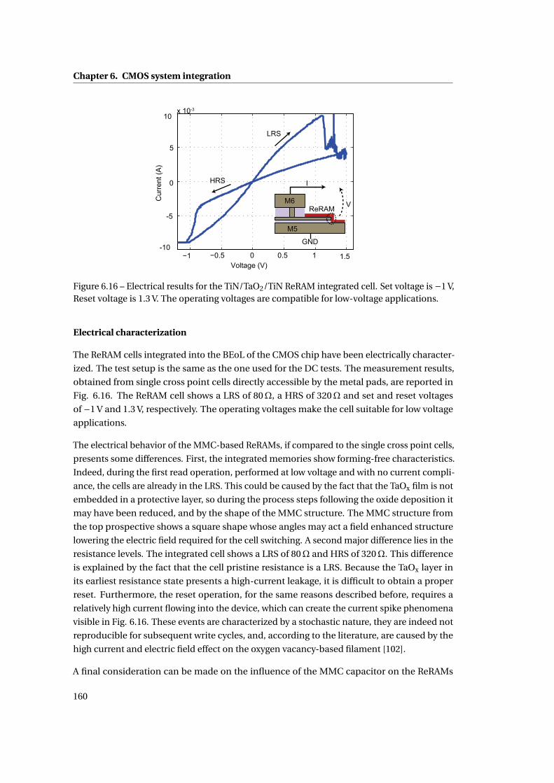
Chapter 6. CMOS system integration
Figure 6.16 – Electrical results for the TiN/TaO2/TiN ReRAM integrated cell. Set voltage is −1 V,Reset voltage is 1.3 V. The operating voltages are compatible for low-voltage applications.
Electrical characterization
The ReRAM cells integrated into the BEoL of the CMOS chip have been electrically character-
ized. The test setup is the same as the one used for the DC tests. The measurement results,
obtained from single cross point cells directly accessible by the metal pads, are reported in
Fig. 6.16. The ReRAM cell shows a LRS of 80Ω, a HRS of 320Ω and set and reset voltages
of −1 V and 1.3 V, respectively. The operating voltages make the cell suitable for low voltage
applications.
The electrical behavior of the MMC-based ReRAMs, if compared to the single cross point cells,
presents some differences. First, the integrated memories show forming-free characteristics.
Indeed, during the first read operation, performed at low voltage and with no current compli-
ance, the cells are already in the LRS. This could be caused by the fact that the TaOx film is not
embedded in a protective layer, so during the process steps following the oxide deposition it
may have been reduced, and by the shape of the MMC structure. The MMC structure from
the top prospective shows a square shape whose angles may act a field enhanced structure
lowering the electric field required for the cell switching. A second major difference lies in the
resistance levels. The integrated cell shows a LRS of 80Ω and HRS of 320Ω. This difference
is explained by the fact that the cell pristine resistance is a LRS. Because the TaOx layer in
its earliest resistance state presents a high-current leakage, it is difficult to obtain a proper
reset. Furthermore, the reset operation, for the same reasons described before, requires a
relatively high current flowing into the device, which can create the current spike phenomena
visible in Fig. 6.16. These events are characterized by a stochastic nature, they are indeed not
reproducible for subsequent write cycles, and, according to the literature, are caused by the
high current and electric field effect on the oxygen vacancy-based filament [102].
A final consideration can be made on the influence of the MMC capacitor on the ReRAMs
160
6.5. ReRAM chip-level integration
switch characteristic. The capacitance has a value of 3.6 fF and it is electrically connected in
parallel to the ReRAM cell. The resulting RC time constant is less than 1 ps, making it negligible
if compared with the time scale of the observed phenomena. This time is indeed much faster
than the voltage ramp time step used for the I-V sweep measurement and faster than any
reported value for the ReRAM switching time. Furthermore, there was no need for a forming
operation, which is the procedure that is the most sensitive to the current overshoots created
by the line parasitics and by the setup, and the set operation was limited by the parasitic
resistances in series with the ReRAM cell, so there was not an abrupt resistance change when
reaching the current compliance. Moreover, this device configuration is not different from the
VIA-based cell configuration. In that case, the capacitance created by the electrode surface was
also in parallel with the ReRAM cell, and in that case the analytically calculated capacitance
value is around 100 times larger than the MMC one. Because of these considerations we
can conclude that the influence of the MMC capacitor on the electrical characteristics of the
ReRAM cell are negligible.
6.5.2 Top-metal integration approach
The second integration method is based on a top-metal integration approach. The goal is
to reproduce the same process used for the VIA-based ReRAM cells described in Section 3.4
on the top metal of a CMOS chip. If compared to the integration method presented before,
this one allows more flexibility on parameters such as: ReRAM material thickness, electrode
material and cell geometry. This has been carried out on a chip containing just passive features,
which is used to validate the process flow and to characterize the integrated memories. This
process flow can be easily adapted to several ReRAMs material stacks. In order to calibrate
the process, we decided to fabricate TiN (100 nm)/TaOx (25 nm)/TiN (100 nm) memories. A
TiN BE is used because it is easier to etch with respect to a Pt one, and the TaOx switching film
is preferred to HfO2 as it gave better performances with the TiN BE. In the following text, we
present the integration process flow and the electrical results.
Integration process flow
The fabrication of the carrier wafer is similar to the one presented for the MMC-based ap-
proach described in Subsection 6.5.1. After the DRIE, instead of depositing the parylene layer,
we fixed the chip with Quickstick. The integration process continues then as follows.
First, the 1μm SiO2 passivation of the chip is selectively etched away by a C4F8-based ICP RIE.
Then, the TiN BE is deposited at room temperature by magnetron sputtering and patterned
via ICP RIE using the same recipe described before for the stand alone devices (Section 3.4). A
100 nm SiO2 passivation layer is then deposited by room temperature sputtering and etched
away by BHF. This passivation layer defines the shape and the size of the ReRAM memory.
We decided to pattern VIAs with diameters ranging from 2μm to 15μm. The ReRAM stack is
finally finished by the deposition and patterning of the TaOx resistive material and the TiN TE.
161
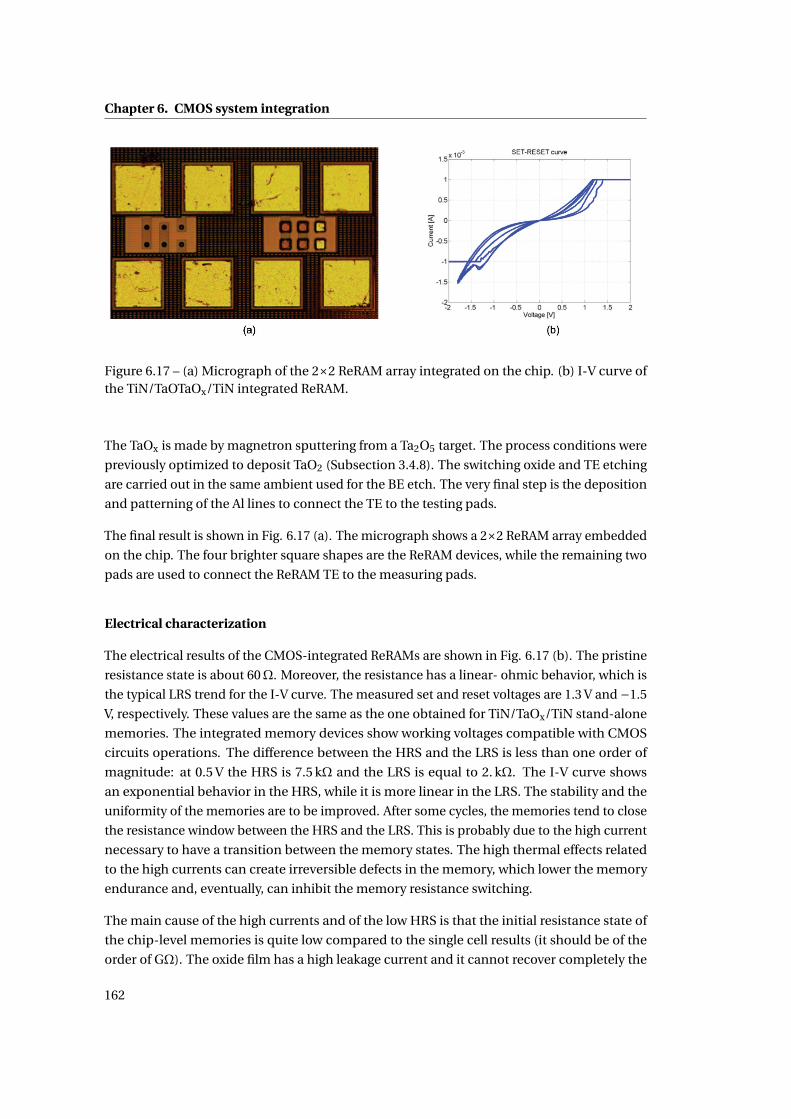
Chapter 6. CMOS system integration
Figure 6.17 – (a) Micrograph of the 2×2 ReRAM array integrated on the chip. (b) I-V curve ofthe TiN/TaOTaOx/TiN integrated ReRAM.
The TaOx is made by magnetron sputtering from a Ta2O5 target. The process conditions were
previously optimized to deposit TaO2 (Subsection 3.4.8). The switching oxide and TE etching
are carried out in the same ambient used for the BE etch. The very final step is the deposition
and patterning of the Al lines to connect the TE to the testing pads.
The final result is shown in Fig. 6.17 (a). The micrograph shows a 2×2 ReRAM array embedded
on the chip. The four brighter square shapes are the ReRAM devices, while the remaining two
pads are used to connect the ReRAM TE to the measuring pads.
Electrical characterization
The electrical results of the CMOS-integrated ReRAMs are shown in Fig. 6.17 (b). The pristine
resistance state is about 60Ω. Moreover, the resistance has a linear- ohmic behavior, which is
the typical LRS trend for the I-V curve. The measured set and reset voltages are 1.3 V and −1.5
V, respectively. These values are the same as the one obtained for TiN/TaOx/TiN stand-alone
memories. The integrated memory devices show working voltages compatible with CMOS
circuits operations. The difference between the HRS and the LRS is less than one order of
magnitude: at 0.5 V the HRS is 7.5 kΩ and the LRS is equal to 2. kΩ. The I-V curve shows
an exponential behavior in the HRS, while it is more linear in the LRS. The stability and the
uniformity of the memories are to be improved. After some cycles, the memories tend to close
the resistance window between the HRS and the LRS. This is probably due to the high current
necessary to have a transition between the memory states. The high thermal effects related
to the high currents can create irreversible defects in the memory, which lower the memory
endurance and, eventually, can inhibit the memory resistance switching.
The main cause of the high currents and of the low HRS is that the initial resistance state of
the chip-level memories is quite low compared to the single cell results (it should be of the
order of GΩ). The oxide film has a high leakage current and it cannot recover completely the
162
6.6. Summary
HRS. Typically, two ways are possible to increase the resistive state of the oxide: increasing the
thickness of the oxide layer or increasing the oxygen flux during the deposition of the oxide.
Both these solutions have been investigated by fabricating a chip with a TaO2 layer of 50 nm
deposited using a recipe with oxygen flux. Despite these modifications in the memory layer,
the initial state of these modified ReRAMs is still at a LRS (the value is not higher than few
hundreds of Ohms).
A FIB cross-section analysis has been carried out to spot eventual short circuits between the
electrode layers. The result suggests (not shown) a clear separation between the electrode
layers, so the reason for the memory low initial resistance state should be investigated else-
where. The oxide deposition conditions, the material stack, the device geometry and the
etching processes were the same as the process used for the stand-alone memories, so they
are probably not the direct cause of the low pristine resistance state. It is believed that the
most probable reason for the failure of the resistances is the TE RIE etching process. This
problem is similar to the one we have for the single cells fabricated on dies, and it could be
overcome by modifying the etching parameters.
6.6 Summary
In this section we summarize the information presented in this chapter.
We first model the electrical characteristics obtained from the fabricated devices with a Verilog-
A compact model. This is used for the design and simulation of the CMOS read and write
circuit.
We present a read circuit designed to reduce the sneak-path currents in a ReRAM crossbar array
configuration. The circuit forces the potential drop across the unselected devices to a value
close to zero, reducing the sneak-path currents by a factor 10. This is obtained applying the
same voltage value at the device electrodes and compensating the technological mismatches
with a calibration circuit.
A second approach to reduce the the sneak-path currents is add a selector device in series
to the memory cell. We show the fabrication and characterization of Pt/VO2/Pt selectors.
Moreover, we integrate the VO2-based devices in a 1S1R configuration together with the
fabricated ReRAMs, demonstrating a cut-off of the sneak-path currents of a factor 10.
Finally, we show the integration of ReRAM devices with standard CMOS chips. We discuss the
fabrication steps and the electrical results of two prototype approaches to obtain a heteroge-
neous integration of ReRAMs and CMOS.
163


7 Conclusion and future work
In this thesis we discussed the design, fabrication, characterization and integration of ReRAM
devices. The main subject is the qualitative and quantitative analysis of the main factors
that influence the resistive memory electrical behavior. Such factors are related either to the
memory fabrication, either to the test environment.
This is obtained by developing a fixed research framework that drives the device optimization
and allows to compare the results obtained from different ReRAMs. This methodology invests
the whole device development by introducing standards in the fabrication process, electrical
setups, data treatment and data analysis.
We first analyze the effects that variations in the fabrication process steps, device geometry and
composition have on the memory electrical characteristics. In details, several BEs, switching
materials, buffer layers, and TEs have been investigated and discussed. Furthermore, we
analyzed the effects of differed device sizes, passivation films, TE patterning and annealing
processes. After the discussion of each variation, we use the obtained database to gather in-
sights on the ReRAM working mechanism and the adopted methodology by using a correlation
analysts.
We then discuss the influence of the test conditions over the ReRAM behavior. We show how
the set pulse voltage, reset pulse voltage, current compliance, pulse width and pulse rising time
can influence the memory reliability. Furthermore, we show how these factors can influence
the memory resistance states, and we propose an empirical model to describe such changes.
We also show how it is possible to control the resistance states by modulating the number of
input pulses applied to the device.
The second subject of this work is the integration of the fabricated devices in a CMOS tech-
nology environment for passive crossbar configurations. We present a Verilog-A model used
to simulate the device characteristics. We also show two solutions to limit the sneak-path
currents for ReRAMs: a dedicated read circuit and the development of selector devices. We
describe the selector fabrication, as well as the electrical characterization and the combination
165

Chapter 7. Conclusion and future work
SRAM DRAMFlash
ReRAMNOR NAND
Cell Area >100 F2 6 F2 10 F2 4 F2 4 F2 - 45 nm
Voltage <1 V <1 V >10 V >10 V −2 V-1.5 V
Read time ~1 ns ~10 ns ~50 ns ~10μs <30 ns ?
Write time ~1 ns ~10 ns 10μs-1 ms 100μs-1 ms <30 ns
Retention N/A ~64 ms >10 y >10 y >4 y ?
Endurance >1016 >1016 >105 >104 >>104
Write energy (J/bit) ~fJ ~10 fJ ~100 pJ ~10 fJ ~0.9 pJ
Table 7.1 – Summary and comparison of the fabricated device performances.
with our ReRAMs in a 1S1R configuration. Finally, we show two methods to integrate ReRAM
devices in the BEoL of CMOS chips.
The performances of the fabricated ReRAMs are summarized in Table 7.1. The cell area,
endurance and retention are comparable to NAND Flash, while the device speed and operating
voltages are close to the DRAM ones. The only parameter that is higher compared to NAND
and DRAM is the write energy.
During the course of this thesis, the following novelties have been presented:
• The description of a research methodology that separate the effects on the device
characteristics of different cell structures and setup parameters by DC and pulse tests,
respectively (Section 4.1 and Section 5.1).
• The development of a custom TiN dry etching recipe with optimized selectivity and
taper angle (Subsection 3.4.4).
• The comparison between the electrical characteristics of ReRAM cells operated in cur-
rent and voltage mode (Section 4.3).
• The analysis of the effects of the buffer layer thickness on the forming voltage (Subsec-
tion 4.4.3).
• The effects of the memory passivation material on the ReRAM electrical behavior (Sub-
section 4.4.4).
• The effects of the post metallization annealing on the ReRAM electrical behavior (Sub-
section 4.4.6).
• The correlation analysis between the ReRAM electrical parameters (Section 4.5).
• The statistical analysis to determine the influence of the test conditions over the ReRAM
electrical behavior (Section 5.5).
166

• The integration or ReRAM memories in the BEoL of fully finished 180 nm CMOS foundry
chip (Section 6.5).
Future work
We believe that several additions could be implemented to further improve this work.
Regarding the test methodology, it may be beneficial to change the pulse setup by sending the
pulse signal to the transistor gate instead of to the TE. This would result in a better control
of the setup delays. Moreover, in order to obtain endurance data, it would be necessary to
optimize the parameters to switch the cell with the transistor in series also the reset operation.
This would allow to use 3-level pulses, which would greatly decrease the amount of GPIB
communication.
For the device fabrication, the next step would be to merge the die-based process and the
e-beam lithography one. This would allow to combine the benefit of the two, allowing a fast
prototyping and nanometer-size VIA openings. The die-based process was already designed
by taking into account this possibility, as we included a mask to make the e-beam alignment
marks. Regarding the ReRAM memory fabrication, more efforts should be dedicated in the
development of a reliable technology using TiN as BE.
The next step in the DC characterization would the modeling of the effects of the process
variations. These data were indeed just considered in a qualitative way. In order to extract an
empirical model, there is the need to link the process changes to physics-based variables. For
example, resistive layers of different materials and thicknesses could be described, in order to
model the forming voltage, by their tunnel probability and oxygen affinity. It is also possible
to expand the analysis to countless new materials or process combinations. Moreover, as
mentioned in the text, it would be interesting to compare the data obtained for the correlation
analysis with the available ReRAM models, in order to verify or improve them.
Regarding the pulse measurements and resistance modulation, more work can be done in
improving the models that describe the resistance changes with respect to the test inputs.
It would be interesting to consider exponential relations, and not limit the analysis to just
linear models. More characterization is also needed for the resistance change obtained by
modulating the number of input pulses applied to the device.
Finally, many improvements can be made on the selector and CMOS integration, as the work
on these topics can be considered as preliminary at most. The process flow for fabricating
VO2-based devices should be improved with regard to the device thickness, thermal budget
and by developing the film etching. Second order improvements can be considered the doping
of the VO2 film in order to improve the matching with the ReRAM characteristics. Finally, a
process to monolitically integrate the ReRAM with the selector should be developed. The
ReRAM-CMOS integration should also be improved, as currently there are issues with the TE
167

Chapter 7. Conclusion and future work
etching and the embedding of the die in the carrier wafer.
168

A Characterization methodology
This annex describes the research methodology followed for this work. Here the general
research flow and the adopted standardization are presented. The developed research frame-
work allows to drive the device optimization and to compare the results obtained from different
ReRAM cells and test conditions.
This chapter is divided as follows. First, in Section A.1, we discuss the electrical measurement
setups used to test the fabricated devices. This will follow by the description of the functions
used for the data treatment, which involve the extraction of the key memory parameters from
the test raw data, presented in Section A.2. Next, in Section A.3, we describe the structure of
the database obtained from the electrical tests. Finally, in Section A.4, we show the tools and
functions used for the data analysis.
A.1 Electrical test setups
The electrical characterization of the fabricated devices is carried out with a probe station in
a dark room environment. The great majority of the results presented in this document are
performed with the DC and pulse setup described in Fig. A.1.
The main objective of the DC tests, as it is described in details in Chapter 4, is to determine the
impact of the device material and structure on its electrical characteristics. In order to access
this, it is important to follow a determined test procedure. It is critical that the test is constant
for all the devices, so that it does not introduce unwanted variations in the ReRAM electrical
behavior.
The DC test setup, schematized in Fig. A.1 (a), includes a Keysight B1500 semiconductor device
analyzer controlled by the Keysight software EasyEXPERT. The voltage is applied on the ReRAM
TE, while the BE is set to ground. Triaxial cables are used to connect the high-resolution Source
Measure Unit (SMU) modules to the probes in order to lower the setup parasitics and to reduce
the current overshoots. The DC tests serve the following standard procedure. First, a forming
operation is performed on the device by a double voltage ramp from 0 to 5 V with a 5 mV step
169
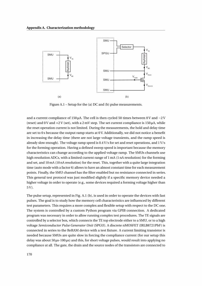
Appendix A. Characterization methodology
Figure A.1 – Setup for the (a) DC and (b) pulse measurements.
and a current compliance of 150μA. The cell is then cycled 50 times between 0 V and −2 V
(reset) and 0 V and +2 V (set), with a 2 mV step. The set current compliance is 150μA, while
the reset operation current is not limited. During the measurements, the hold and delay time
are set to 0 s because the output ramp starts at 0 V. Additionally, we did not notice a benefit
in increasing the delay time (there are not large voltage transients, and the ramp speed is
already slow enough). The voltage ramp speed is 0.4 V/s for set and reset operations, and 1 V/s
for the forming operation. Having a defined sweep speed is important because the memory
characteristics can change according to the applied voltage ramp. The SMUs channels use
high resolution ADCs, with a limited current range of 1 mA (1 nA resolution) for the forming
and set, and 10 mA (10 nA resolution) for the reset. This, together with a quite large integration
time (auto mode with a factor 6) allows to have an almost constant time for each measurement
points. Finally, the SMU channel has the filter enabled but no resistance connected in series.
This general test protocol was just modified slightly if a specific memory device needed a
higher voltage in order to operate (e.g., some devices required a forming voltage higher than
5 V).
The pulse setup, represented in Fig. A.1 (b), is used in order to operate the devices with fast
pulses. The goal is to study how the memory cell characteristics are influenced by different
test parameters. This requires a more complex and flexible setup with respect to the DC one.
The system is controlled by a custom Python program via GPIB connection. A dedicated
program was necessary in order to allow running complex test procedures. The TE signals are
controlled by a selector box, which connects the TE top electrode either to a SMU, or to a high
voltage Semiconductor Pulse Generator Unit (SPGU). A discrete nMOSFET (IRLB8721PbF) is
connected in series to the ReRAM device with a test fixture. A current limiting transistor is
needed because SMUs are quite slow in forcing the compliance current (for our setup this
delay was about 50μs-100μs) and this, for short voltage pulses, would result into applying no
compliance at all. The gate, the drain and the source nodes of the transistors are connected to
170
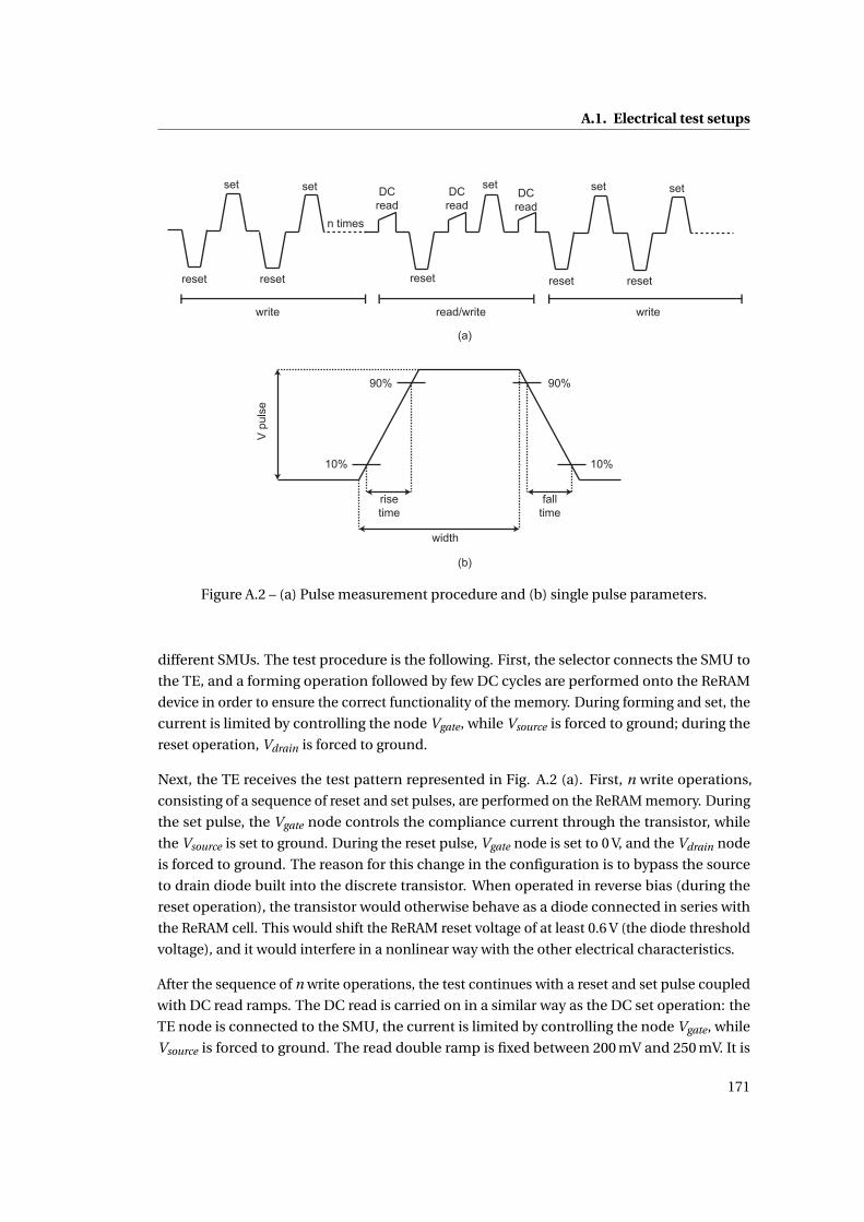
A.1. Electrical test setups
Figure A.2 – (a) Pulse measurement procedure and (b) single pulse parameters.
different SMUs. The test procedure is the following. First, the selector connects the SMU to
the TE, and a forming operation followed by few DC cycles are performed onto the ReRAM
device in order to ensure the correct functionality of the memory. During forming and set, the
current is limited by controlling the node Vgate, while Vsource is forced to ground; during the
reset operation, Vdrain is forced to ground.
Next, the TE receives the test pattern represented in Fig. A.2 (a). First, n write operations,
consisting of a sequence of reset and set pulses, are performed on the ReRAM memory. During
the set pulse, the Vgate node controls the compliance current through the transistor, while
the Vsource is set to ground. During the reset pulse, Vgate node is set to 0 V, and the Vdrain node
is forced to ground. The reason for this change in the configuration is to bypass the source
to drain diode built into the discrete transistor. When operated in reverse bias (during the
reset operation), the transistor would otherwise behave as a diode connected in series with
the ReRAM cell. This would shift the ReRAM reset voltage of at least 0.6 V (the diode threshold
voltage), and it would interfere in a nonlinear way with the other electrical characteristics.
After the sequence of n write operations, the test continues with a reset and set pulse coupled
with DC read ramps. The DC read is carried on in a similar way as the DC set operation: the
TE node is connected to the SMU, the current is limited by controlling the node Vgate, while
Vsource is forced to ground. The read double ramp is fixed between 200 mV and 250 mV. It is
171

Appendix A. Characterization methodology
Figure A.3 – Oscilloscope data of a 50Ω resistor in series to TiN/TaO2 (25 nm)/TiN ReRAM cellduring the forming operation: the parameter analyzer 500μA current compliance is reachedjust after 70μs and with a peak current of 1.2 mA.
important to define a standard read voltage because the ReRAM HRS varies exponentially with
respect to the voltage (the lower the read voltage, the higher the HRS). The read operation is
used in order to determine the resistance before and after each write pulse. The resistance is
calculated as the mean of the resistance values obtained by dividing the voltage by the current
for 50 measurement points in the 200 mV - 250 mV interval. The test continues then with
another series of n write operations, and the procedure repeats itself until the end of the test.
The definition of the pulse parameters that has been changed during the test are reported in
Fig. A.2 (b). These definitions are consistent with the one adopted by Keysight.The rise time
and the fall time are defined as the 10% to 90% variation of the signal, while the pulse width is
defined as the sum of the signal ramp plus the time the signal stays at the V pulse voltage level.
It is important to notice that the definition of the signal width and the rise time are related to
each other.
The two setups described above have the following limitations. The DC one is quite susceptible
to current overshoots during the forming operation due to the lack of a series transistor. An
example of the overshoot current for a TiN/TaO2 (25 nm)/TiN ReRAM is reported in Fig. A.3.
The current, monitored through a 50Ω resistor in series to the memory cell, shows that the
parameter analyzer 500μA current compliance is reached just after 70μs, and the current
reaches a peak of 1.2 mA. This result represents one of the limit cases: as the forming voltage
for this specific ReRAM is very high (12 V), the resulting current peak reaches high values.
The overshoot effects have been monitored and considered during the data statistic, as it is
described in details in Chapter 4.
The pulse setup has limits in the minimum pulse speed and the maximum number of pulses.
The fastest pulse we could send to the memory device has a width of 20 ns. Below 50 ns the
signal is highly distorted due to the setup parasitic, and it requires corrections both in the
signal shape and height. The maximum number of write operation we can send to the memory
172
A.2. Data treatment functions
is about 50 k cycles. This limit comes from the failure of the GPIB communication caused by
the large amount of communication needed for the different set and reset configurations. A
possible solution for this would be to adopt 3-level pulses, but this would imply to have the
same set and reset arrangements. Because we wanted to avoid having the transistor diode in
series during the reset operation, we decided not to implement this solution.
A.2 Data treatment functions
After the testing of the devices, the raw data need to be processed in order to extract the
parameters of interest. This process should be consistent throughout all the test results,
as the adopted standardization has an influence on the final outcome of the analysis. The
data processing is different between DC and pulse tests because both the raw data and the
parameters obtained are specific for each test type.
For the DC tests, the parameter analyzer creates one .csv file for each operation, i.e., forming,
set or reset. The file includes the parameter analyzer settings and, for each measurement
point, the time, the voltage and the current. We first process these files via a Matlab script by
removing all the information but the voltage and current data, and by converting the files into
a .dat format. The obtained collection of files is then ordered and loaded into the OriginLab
software. A custom OriginLab script reads the .dat files corresponding to a ReRAM device full
test procedure, which involves a forming operation and 50 set-reset cycles. The script then
launches a routine that results in the summary plots reported in Fig. A.4. From top left to
bottom right, the plots are described hereafter.
Fig. A.4 (a) shows the basic I-V curve of the ReRAM device. The forming and the first reset
are marked in red in order to highlight the forming voltage and an eventual effects of current
overshoots (typically considered about equal to the maximum current reached for the first
reset [63]). Fig. A.4 (b) shows the R-V curve of the device. The resistance data are obtained
for each measurement point by dividing the voltage by the corresponding current value. The
obtained number is then a static resistance, and not a differential one. From the figure it
is possible to observe the exponential relation between the HRS and the voltage, that was
described in Section 2.3. Fig. A.4 (c) shows the cycle-to-cycle resistance of the device. The
values are obtained by selecting the device resistance at 250 mV in order to be consistent with
the read voltage used during the pulse measurements (see Section A.1). More precisely, the
LRS is calculated at −250 mV, while the HRS is calculated at +250 mV, since the ADC used to
measure the current for the positive ramp (during set and forming) has a higher resolution, as
explained in Section A.1. An histogram with the relative frequency of the resistance states is
reported in Fig. A.4 (d). The plot shows how the resistance states are distributed in a linear
scale. A similar information is reported in the cumulative probability plot reported in Fig. A.4
(e). For this figure, each resistance measurement is plotted on the x-axis against the fraction
of all the the resistance values that are less than or equal to that measurement. This allows
to read off the probability of being above or below a particular value, or of being within, or
173
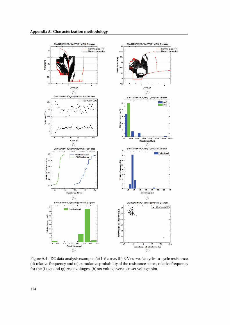
Appendix A. Characterization methodology
Figure A.4 – DC data analysis example: (a) I-V curve, (b) R-V curve, (c) cycle-to-cycle resistance,(d) relative frequency and (e) cumulative probability of the resistance states, relative frequencyfor the (f) set and (g) reset voltages, (h) set voltage versus reset voltage plot.
174
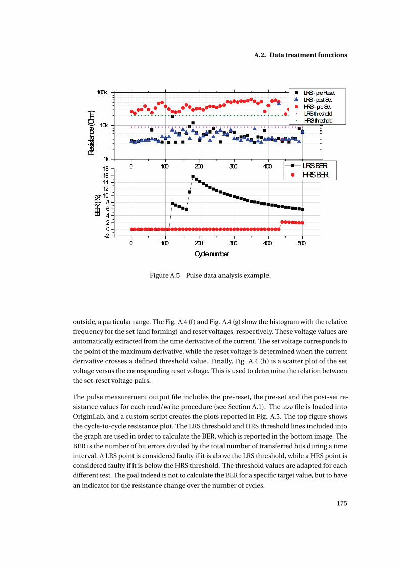
A.2. Data treatment functions
Figure A.5 – Pulse data analysis example.
outside, a particular range. The Fig. A.4 (f) and Fig. A.4 (g) show the histogram with the relative
frequency for the set (and forming) and reset voltages, respectively. These voltage values are
automatically extracted from the time derivative of the current. The set voltage corresponds to
the point of the maximum derivative, while the reset voltage is determined when the current
derivative crosses a defined threshold value. Finally, Fig. A.4 (h) is a scatter plot of the set
voltage versus the corresponding reset voltage. This is used to determine the relation between
the set-reset voltage pairs.
The pulse measurement output file includes the pre-reset, the pre-set and the post-set re-
sistance values for each read/write procedure (see Section A.1). The .csv file is loaded into
OriginLab, and a custom script creates the plots reported in Fig. A.5. The top figure shows
the cycle-to-cycle resistance plot. The LRS threshold and HRS threshold lines included into
the graph are used in order to calculate the BER, which is reported in the bottom image. The
BER is the number of bit errors divided by the total number of transferred bits during a time
interval. A LRS point is considered faulty if it is above the LRS threshold, while a HRS point is
considered faulty if it is below the HRS threshold. The threshold values are adapted for each
different test. The goal indeed is not to calculate the BER for a specific target value, but to have
an indicator for the resistance change over the number of cycles.
175
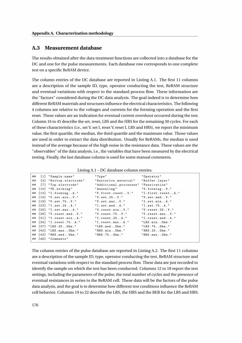
Appendix A. Characterization methodology
A.3 Measurement database
The results obtained after the data treatment functions are collected into a database for the
DC and one for the pulse measurements. Each database row corresponds to one complete
test on a specific ReRAM device.
The column entries of the DC database are reported in Listing A.1. The first 11 columns
are a description of the sample ID, type, operator conducting the test, ReRAM structure
and eventual variations with respect to the standard process flow. These information are
the "factors" considered during the DC data analysis. The goal indeed is to determine how
different ReRAM materials and structures influence the electrical characteristics. The following
4 columns are relative to the voltages and currents for the forming operation and the first
reset. These values are an indication for eventual current overshoot occurred during the test.
Column 16 to 45 describe the set, reset, LRS and the HRS for the remaining 50 cycles. For each
of these characteristics (i.e., set V, set I, reset V, reset I, LRS and HRS), we report the minimum
value, the first quartile, the median, the third quartile and the maximum value. Those values
are used in order to extract the data distribution. Usually for ReRAMs, the median is used
instead of the average because of the high noise in the resistance data. These values are the
"observables" of the data analysis, i.e., the variables that have been measured by the electrical
testing. Finally, the last database column is used for some manual comments.
Listing A.1 – DC database column entries.
## [1] "Sample.name" "Type" "Operator"## [4] "Bottom.electrode" "Resistive.material" "Buffer.layer"## [7] "Top.electrode" "Additional.processes" "Passivation"## [10] "TE.etching" "Annealing" "V.forming ..V."## [13] "I.forming ..A." "V.first.reset..V." "I.first.reset..A."## [16] "V.set.min..V." "V.set .25..V." "V.set.med..V."## [19] "V.set .75..V." "V.set.max..V." "I.set.min..A."## [22] "I.set .25..A." "I.set.med..A." "I.set .75..A."## [25] "I.set.max..A." "V.reset.min..V." "V.reset .25..V."## [28] "V.reset.med..V." "V.reset .75..V." "V.reset.max..V."## [31] "I.reset.min..A." "I.reset .25..A." "I.reset.med..A."## [34] "I.reset .75..A." "I.reset.max..A." "LRS.min..Ohm."## [37] "LRS .25.. Ohm." "LRS.med..Ohm." "LRS .75.. Ohm."## [40] "LRS.max..Ohm." "HRS.min..Ohm." "HRS .25.. Ohm."## [43] "HRS.med..Ohm." "HRS .75.. Ohm." "HRS.max..Ohm."## [46] "Comments"
The column entries of the pulse database are reported in Listing A.2. The first 11 columns
are a description of the sample ID, type, operator conducting the test, ReRAM structure and
eventual variations with respect to the standard process flow. These data are just recorded to
identify the sample on which the test has been conducted. Columns 12 to 18 report the test
settings, including the parameters of the pulse, the total number of cycles and the presence of
eventual resistances in series to the ReRAM cell. These data will be the factors of the pulse
data analysis, and the goal is to determine how different test conditions influence the ReRAM
cell behavior. Columns 19 to 22 describe the LRS, the HRS and the BER for the LRS and HRS.
176
A.4. Data analysis functions
These data describes the observables of the analysis. Finally, the last two columns are for the
read voltage value and for manual comments.
Listing A.2 – Pulse database entries.
## [1] "Sample.name" "Type" "Test.date"## [4] "Cell" "Test .." "Operator"## [7] "Bottom.electrode" "Resistive.material" "Buffer.layer"## [10] "Top.electrode" "Additional.processes" "V.Reset ..TE."## [13] "V.Set..TE." "Gate.V" "Width ..us."## [16] "Slope" "Series.R" "Cycle .."## [19] "LRS" "Final.LRS.BER" "HRS"## [22] "Final.HRS.BER" "Read.V" "Comments"
A.4 Data analysis functions
In order to determine if a factor is related to an observable it is needed to perform a statistical
analysis on the data. More in detail, we need to address which factor influences a particular
observable, what is the relevance of this relation, and how this relation can be quantified.
In this section we introduce the main statistical concepts and operations that are used in
this work. The detailed discussion of the data analysis results will be reported in Chapter 4
and Chapter 5. This section is divided as follows: Subsection A.4.1 describes the correlation
coefficient and the significance tests, Subsection A.4.2 introduces the analysis of variance and
Subsection A.4.3 reports the regression models that have been considered.
The whole data analysis for the DC and pulse database is carried on using the software R.
A.4.1 Pearson’s correlation coefficient
A correlation test has been used to determine if the factors or the observables are themselves
correlated. For example, we applied a correlation test on the set and reset voltages in order to
determine the relation of these two observables. More in details, we calculated the Pearson’s
product-moment correlation coefficient, which is a measure of the linear correlation between
two variables X and Y. This coefficient has a value between +1 and −1, where +1 is total
positive linear correlation, 0 is no linear correlation, and −1 is total negative linear correlation.
For a population, it is calculated using the Equation A.1, while for a sample is defined as
reported in Equation A.2.
ρ = cov(X ,Y )
σY σY(A.1)
177

Appendix A. Characterization methodology
r =
n∑i=1
(xi − x)(yi − y
)√
n∑i=1
(xi − x)2
√n∑
i=1
(yi − y
)2
, (A.2)
where ρ is the population correlation coefficient, cov is the covariance, σ is the standard
deviation, r is the sample correlation coefficient, n is the sample size, xi and yi are the entries
of the dataset, and x and y are the sample means.
ρ is the correlation among a population, which is a set of similar items, for example the set
and reset voltages in ReRAM cells. Because the tests we can perform on the devices are limited,
we can just access a subset, or sample, of the studied population. The number calculated from
the sample data is then r , i.e., the sample correlation coefficient. r can be interpreted as the
estimate of the unknown population correlation coefficient ρ. The reliability of this estimation
depends both on the coefficient value and the sample size.
In order to determine the significance of the obtained correlation coefficient, it is possible to
apply a t-test. This test allows to decide whether the value of ρ is "close to 0" or "significantly
different from 0" based on r and n. If the test determines that ρ is significantly different from 0,
we can conclude that the correlation coefficient is significant, and that we can use a regression
to model the relationship. In other words, the sample population can be representative of
the whole population, and ρ can be approximated with r . An example of t-test output for the
correlation between the set and reset voltage is reported in Listing A.3.
Listing A.3 – Correlation test example.
#### Pearson ’s product -moment correlation#### data: myData.subset$V.set.med..V. and myData.subset$V.reset.med..V.## t = -10.55, df = 103, p-value < 2.2e-16## alternative hypothesis: true correlation is not equal to 0## 95 percent confidence interval:## -0.8016165 -0.6137952## sample estimates:## cor## -0.7206776
The t-value is a standardized number that is calculated from the sample data during a t-test,
which compares the sample data to what is expected under the null hypothesis (i.e., the
population correlation ρ is close to zero). A t-value of 0 indicates that the sample results
exactly equal the population of the null hypothesis. As the difference between the sample data
and the null hypothesis increases, the absolute value of the t-value increases. The t-value is
178
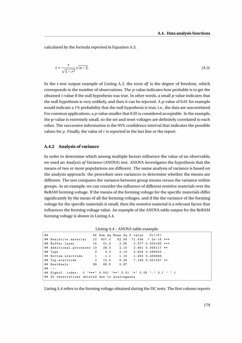
A.4. Data analysis functions
calculated by the formula reported in Equation A.3.
t = r�1− r 2
�n −2. (A.3)
In the t-test output example of Listing A.3, the term df is the degree of freedom, which
corresponds to the number of observations. The p-value indicates how probable is to get the
obtained t-value if the null hypothesis was true. In other words, a small p-value indicates that
the null hypothesis is very unlikely, and then it can be rejected. A p-value of 0.01 for example
would indicate a 1% probability that the null hypothesis is true, i.e., the data are uncorrelated.
For common applications, a p-value smaller that 0.05 is considered acceptable. In the example,
the p-value is extremely small, so the set and reset voltages are definitely correlated to each
other. The successive information is the 95% confidence interval that indicates the possible
values for ρ. Finally, the value of r is reported in the last line or the report.
A.4.2 Analysis of variance
In order to determine which among multiple factors influence the value of an observable,
we used an Analysis of Variance (ANOVA) test. ANOVA investigates the hypothesis that the
means of two or more populations are different. The name analysis of variance is based on
the analysis approach: the procedure uses variances to determine whether the means are
different. The test compares the variance between group means versus the variance within
groups. As an example, we can consider the influence of different resistive materials over the
ReRAM forming voltage. If the means of the forming voltage for the specific materials differ
significantly by the mean of all the forming voltages, and if the the variance of the forming
voltage for the specific materials is small, then the resistive material is a relevant factor that
influences the forming voltage value. An example of the ANOVA table output for the ReRAM
forming voltage is shown in Listing A.4.
Listing A.4 – ANOVA table example.
## Df Sum Sq Mean Sq F value Pr(>F)## Resistive.material 13 807.0 62.08 71.034 < 2e-16 ***## Buffer.layer 14 41.3 2.95 3.377 0.000185 ***## Additional.processes 13 28.0 2.15 2.461 0.006117 **## Type 2 4.2 2.10 2.404 0.095623 .## Bottom.electrode 1 1.1 1.10 1.263 0.263866## Top.electrode 2 12.5 6.26 7.169 0.001237 **## Residuals 99 86.5 0.87## ---## Signif. codes: 0 ’***’ 0.001 ’**’ 0.01 ’*’ 0.05 ’.’ 0.1 ’ ’ 1## 20 observations deleted due to missingness
Listing A.4 refers to the forming voltage obtained during the DC tests. The first column reports
179
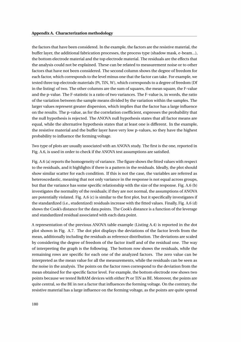
Appendix A. Characterization methodology
the factors that have been considered. In the example, the factors are the resistive material, the
buffer layer, the additional fabrication processes, the process type (shadow mask, e-beam...),
the bottom electrode material and the top electrode material. The residuals are the effects that
the analysis could not be explained. These can be related to measurement noise or to other
factors that have not been considered. The second column shows the degree of freedom for
each factor, which corresponds to the level minus one that the factor can take. For example, we
tested three top electrode materials (Pt, TiN, W), which corresponds to a degree of freedom (Df
in the listing) of two. The other columns are the sum of squares, the mean square, the F-value
and the p-value. The F-statistic is a ratio of two variances. The F-value is, in words, the ratio
of the variation between the sample means divided by the variation within the samples. The
larger values represent greater dispersion, which implies that the factor has a large influence
on the results. The p-value, as for the correlation coefficient, expresses the probability that
the null hypothesis is rejected. The ANOVA null hypothesis states that all factor means are
equal, while the alternative hypothesis states that at least one is different. In the example,
the resistive material and the buffer layer have very low p-values, so they have the highest
probability to influence the forming voltage.
Two type of plots are usually associated with an ANOVA study. The first is the one, reported in
Fig. A.6, is used in order to check if the ANOVA test assumptions are satisfied.
Fig. A.6 (a) reports the homogeneity of variance. The figure shows the fitted values with respect
to the residuals, and it highlights if there is a pattern in the residuals. Ideally, the plot should
show similar scatter for each condition. If this is not the case, the variables are referred as
heteroscedastic, meaning that not only variance in the response is not equal across groups,
but that the variance has some specific relationship with the size of the response. Fig. A.6 (b)
investigates the normality of the residuals; if they are not normal, the assumptions of ANOVA
are potentially violated. Fig. A.6 (c) is similar to the first plot, but it specifically investigates if
the standardized (i.e., studentized) residuals increase with the fitted values. Finally, Fig. A.6 (d)
shows the Cook’s distance for the data points. The Cook’s distance is a function of the leverage
and standardized residual associated with each data point.
A representation of the previous ANOVA table example (Listing A.4) is reported in the dot
plot shown in Fig. A.7. The dot plot displays the deviations of the factor levels from the
mean, additionally including the residuals as reference distribution. The deviations are scaled
by considering the degree of freedom of the factor itself and of the residual one. The way
of interpreting the graph is the following. The bottom row shows the residuals, while the
remaining rows are specific for each one of the analyzed factors. The zero value can be
interpreted as the mean value for all the measurements, while the residuals can be seen as
the noise in the analysis. The points on the factor rows correspond to the deviation from the
mean obtained for the specific factor level. For example, the bottom electrode row shows two
points because we tested ReRAM devices with either Pt or TiN as BE. Moreover, the points are
quite central, so the BE in not a factor that influences the forming voltage. On the contrary, the
resistive material has a large influence on the forming voltage, as the points are quite spread
180
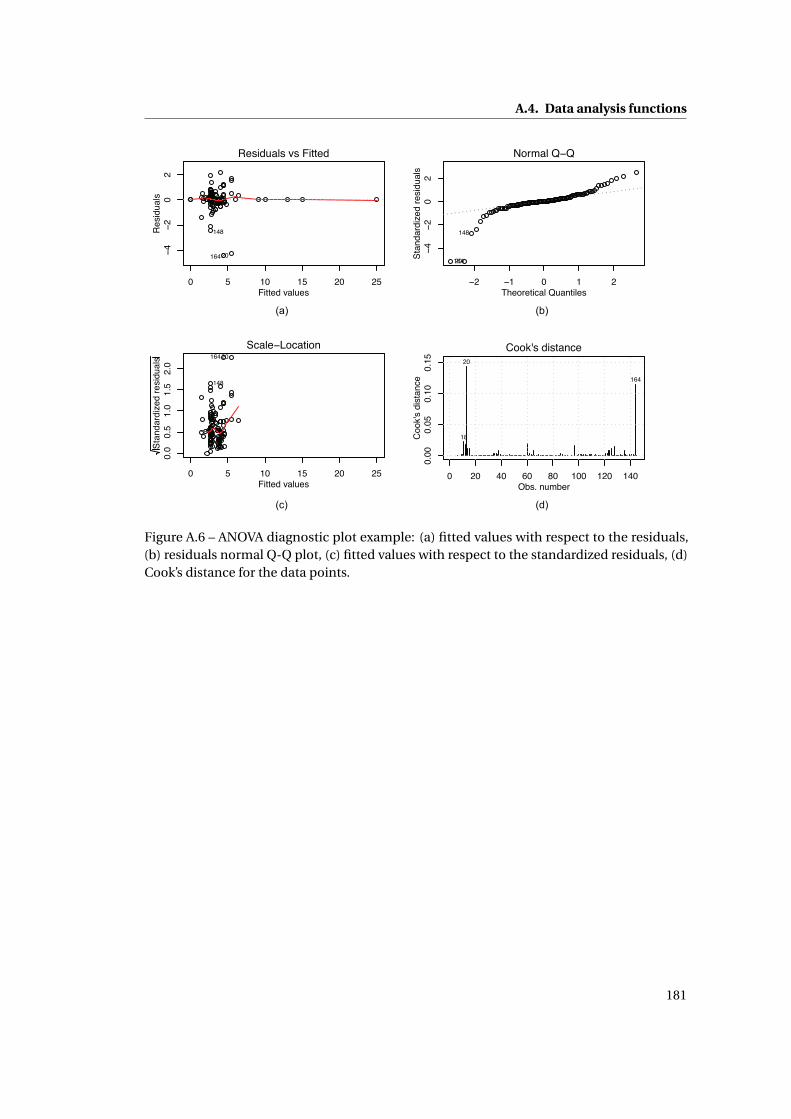
A.4. Data analysis functions
0 5 10 15 20 25
02
Fitted values
Res
idua
lsResiduals vs Fitted
20
0 1 2
02
Theoretical Quantiles
Stan
dard
ized
resi
dual
s
Nor
20
0 5 10 15 20 25
0.0
0.5
1.0
1.5
2.0
Fitted values
Stan
dard
ized
resi
dual
s 20
0 20 60 100 120
0.00
0.05
0.10
0.15
Obs. number
Coo
k's d
ista
nce
Cook's distance20
Figure A.6 – ANOVA diagnostic plot example: (a) fitted values with respect to the residuals,(b) residuals normal Q-Q plot, (c) fitted values with respect to the standardized residuals, (d)Cook’s distance for the data points.
181

Appendix A. Characterization methodology
ANOVA, forming V
Resistive material
Buffer layer
Additional process
Process type
Bottom electrode
Top electrode
Residuals
Figure A.7 – ANOVA plot example: (a) fitted values with respect to the residuals, (b) residualsnormal Q-Q plot, (c) fitted values with respect to the standardized residuals, (d) Cook’s distancefor the data points.
out. This is consistent with the ANOVA table results presented before.
A.4.3 Data regression
Once the main factors that influence a specific output are identified, it is possible to use a data
regression to quantify this relation. The obtained empirical models can be of different types,
but for this work we limit our investigation to linear models. In order to extract the final model
from the possible factors, we used the two algorithms described hereafter.
The first procedure is a stepwise regression. This is an automated tool used in the exploratory
stages of model building to identify a useful subset of predictors. The process systematically
adds the most significant factors or removes the least significant factors during each step.
The second model is a best subsets regression. This is an automated procedure that identifies
the best-fitting regression models with predictors that can be specified before the analysis.
The general approach is to select the smallest subset that fulfills certain statistical criteria.
In general, using a subset of variables instead of a complete set allows an estimate of the
regression coefficients and predict future responses with smaller variance.
The model resulting from the two previously described procedures is then diagnosed by using
182
A.4. Data analysis functions
Formula: log(LRS) = α + β SetV + γ GateV
Coefficient Estimate Std. Error t-value Pr(>F) Signif. code
Intercept (α) 12.3695 0.7098 17.426 < 2e-16 ∗∗∗Set V (β) -1.4619 0.2357 -6.203 1.66e-09 ∗∗∗Gate V (γ) -1.3640 0.3916 -3.483 0.000563 ∗∗∗Signif. codes (according to Pr): [0] -> ∗∗∗; [0.001] -> ∗∗; [0.01] -> ∗; [0.05] -> . ; [0.1] ->
Residual distribution: Min: -0.74040; 1Q: -0.26574; Med: -0.06803; 3Q: 0.21569; Max: 1.30713Residual standard error: 0.367 on 328 degrees of freedomMultiple R-squared: 0.1738, Adjusted R-squared: 0.1688F-statistic: 34.5 on 2 and 328 DF, p-value: 2.523e-14
Table A.1 – Example of a regression model summary.
plots similar to the one showed in Fig. A.6 for the ANOVA analysis. If the analysis validates the
model, the model coefficients and their relative confidence intervals can be extracted.
An example of a regression result summary is reported in Table A.1. The report includes the
model formula, the coefficient estimated values, the standard error for each factor, as well as
the t-value and the p-value. Furthermore, it contains the residual quartile distribution, the
residual standard error, the multiple R-squared values and the F statistic results. The residual
standard error represents the standard deviation of the residuals, so it is a measure of how
close the fit is to the points. The R-squared value is the proportion of the variance in the data
that is explained by the model, while the adjusted value describe the same information, but it
accounts for the number of variables in the model. Finally, The F statistic describes whether
the regression as a whole is performing better than you would expect if all your predictors had
no relationship with the response. This is used to test whether the model outperforms the
measurement noise as a predictor. The reported p-value, as for the previous cases, expresses
the probability that the null hypothesis is rejected.
Additionally, it is possible to estimate the confidence intervals for the coefficients. This is
calculated by multiplying the estimate plus or minus the product of the standard error and the
critical value under the t-distribution with right tail probability at α/2, where α is the lowest
confidence interval probability (e.g., 2.5%).
183


B SKILL code for mask layout
The following SKILL functions have been used for the fabrication mask design in Cadence
Virtuoso.
Listing B.1 – Top level SKILL procedure.
/*add library files*//*add library files*/load(" Procedure_placeCell.il")load(" Procedure_drawNumber.il")
/* project ReRAM -V2, creation of single ReRAM cells for cell charachterization *//* library: ReRAM_SingleCell_V2, cell: device_area_1cm*//* return ID cellview being edited */
cv = geGetEditCellView ()
/*********************************************************************
/* initialization global parameters */tileW = 500 /*tile is the cell area that will be repeated on the wafer */tileH = 500
shiftx_digit_VIA = 50 /* shift of the digit box x0y0 with respect to thecell xy; valid for ReRAM_FPGA: Cell and 200um digit*/
shifty_digit_VIA = 350
shiftx_digit_row = 200 /* shift of the digit box x0y0 with respect to thecell xy; valid for ReRAM_FPGA: Cell and 200um digit*/
shifty_digit_row = 350
shiftx_digit_col = 350 /* shift of the digit box x0y0 with respect to thecell xy; valid for ReRAM_FPGA: Cell and 200um digit*/
shifty_digit_col = 350
tile_dummyLayer = list( "L50" "drawing ") /*layer used for rectangle */cellList = list( "device_cell") /*list of cells to be placed */
/*list values of parametric variables */VIA_diameter_list = list( 1.5 2 3 5 10)
/* counters initialization */count_device = 1 /* counter for device label placement list*/
185
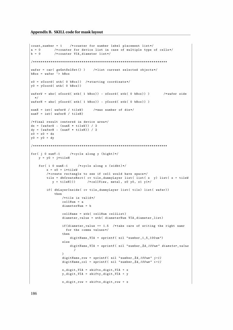
Appendix B. SKILL code for mask layout
count_number = 1 /* counter for number label placement list*/a = 0 /* counter for device list in case of multiple type of cells*/b = 0 /* counter VIA_diameter list*/
/*********************************************************************
wafer = car( geGetSelSet () ) /*list current selected objects */bBox = wafer ~> bBox
x0 = xCoord( nth( 0 bBox)) /* starting coordinate */y0 = yCoord( nth( 0 bBox))
waferW = abs( xCoord( nth( 1 bBox)) - xCoord( nth( 0 bBox)) ) /* wafer side*/
waferH = abs( yCoord( nth( 1 bBox)) - yCoord( nth( 0 bBox)) )
numX = int( waferW / tileW) /*max number of die*/numY = int( waferH / tileH)
/*final result centered in device area*/dx = (waferW - (numX * tileW)) / 2dy = (waferH - (numY * tileH)) / 2x0 = x0 + dxy0 = y0 + dy
/*********************************************************************
for( j 0 numY -1 /*cycle along y (hight)*/y = y0 + j*tileH
for( i 0 numX -1 /*cycle along x (widht)*/x = x0 + i*tileW/* create rectangle to see if cell would have space*/tile = dbCreateRect( cv tile_dummyLayer list( list( x y) list( x + tileW
y + tileH))) /*cellView , metal , x0 y0, x1 y1*/
if( dbLayerInside( cv tile_dummyLayer list( tile) list( wafer))then
/*tile is valid*/cellNum = adiameterNum = b
cellName = nth( cellNum cellList)diameter_value = nth( diameterNum VIA_diameter_list)
if(diameter_value == 1.5 /*take care of writing the right namrfor the comma values */
thendigitName_VIA = sprintf( nil "number _1_5_100 um")
elsedigitName_VIA = sprintf( nil "number_%d_100um" diameter_value
))digitName_row = sprintf( nil "number_%d_100um" j+1)digitName_col = sprintf( nil "number_%d_100um" i+1)
x_digit_VIA = shiftx_digit_VIA + xy_digit_VIA = shifty_digit_VIA + y
x_digit_row = shiftx_digit_row + x
186
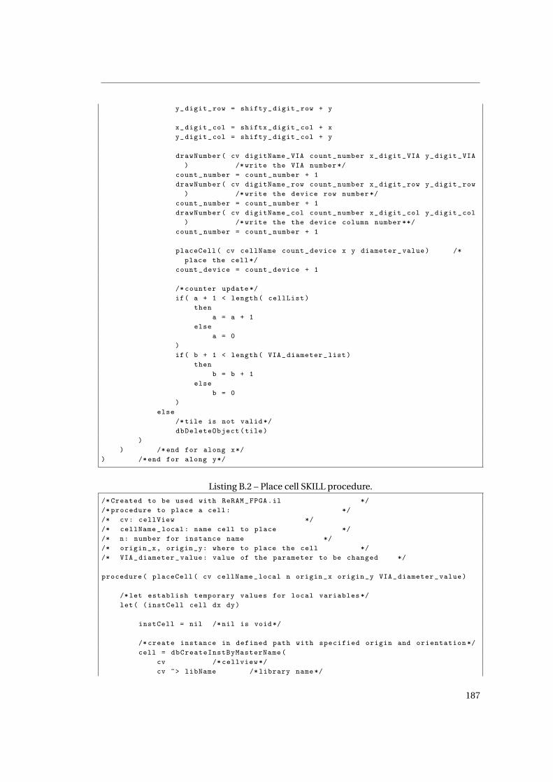
y_digit_row = shifty_digit_row + y
x_digit_col = shiftx_digit_col + xy_digit_col = shifty_digit_col + y
drawNumber( cv digitName_VIA count_number x_digit_VIA y_digit_VIA) /* write the VIA number */
count_number = count_number + 1drawNumber( cv digitName_row count_number x_digit_row y_digit_row
) /* write the device row number */count_number = count_number + 1drawNumber( cv digitName_col count_number x_digit_col y_digit_col
) /* write the the device column number **/count_number = count_number + 1
placeCell( cv cellName count_device x y diameter_value) /*place the cell*/
count_device = count_device + 1
/* counter update */if( a + 1 < length( cellList)
thena = a + 1
elsea = 0
)if( b + 1 < length( VIA_diameter_list)
thenb = b + 1
elseb = 0
)else
/*tile is not valid*/dbDeleteObject(tile)
)) /*end for along x*/
) /*end for along y*/
Listing B.2 – Place cell SKILL procedure.
/* Created to be used with ReRAM_FPGA.il *//* procedure to place a cell: *//* cv: cellView *//* cellName_local: name cell to place *//* n: number for instance name *//* origin_x, origin_y: where to place the cell *//* VIA_diameter_value: value of the parameter to be changed */
procedure( placeCell( cv cellName_local n origin_x origin_y VIA_diameter_value)
/*let establish temporary values for local variables */let( (instCell cell dx dy)
instCell = nil /*nil is void*/
/* create instance in defined path with specified origin and orientation */cell = dbCreateInstByMasterName(
cv /* cellview */cv ~> libName /* library name*/
187
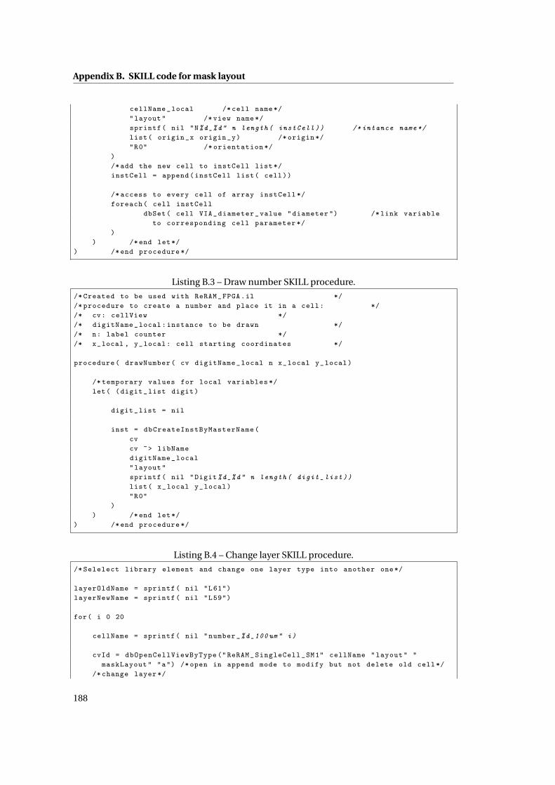
Appendix B. SKILL code for mask layout
cellName_local /*cell name*/"layout" /*view name*/sprintf( nil "N%d_%d" n length( instCell)) /* intance name*/list( origin_x origin_y) /* origin */"R0" /* orientation */
)/*add the new cell to instCell list*/instCell = append(instCell list( cell))
/* access to every cell of array instCell */foreach( cell instCell
dbSet( cell VIA_diameter_value "diameter ") /*link variableto corresponding cell parameter */
)) /*end let*/
) /*end procedure */
Listing B.3 – Draw number SKILL procedure.
/* Created to be used with ReRAM_FPGA.il *//* procedure to create a number and place it in a cell: *//* cv: cellView *//* digitName_local:instance to be drawn *//* n: label counter *//* x_local , y_local: cell starting coordinates */
procedure( drawNumber( cv digitName_local n x_local y_local)
/* temporary values for local variables */let( (digit_list digit)
digit_list = nil
inst = dbCreateInstByMasterName(cvcv ~> libNamedigitName_local"layout"sprintf( nil "Digit%d_%d" n length( digit_list))list( x_local y_local)"R0"
)) /*end let*/
) /*end procedure */
Listing B.4 – Change layer SKILL procedure.
/* Selelect library element and change one layer type into another one*/
layerOldName = sprintf( nil "L61")layerNewName = sprintf( nil "L59")
for( i 0 20
cellName = sprintf( nil "number_%d_100um" i)
cvId = dbOpenCellViewByType ("ReRAM_SingleCell_SM1" cellName "layout" "maskLayout" "a") /*open in append mode to modify but not delete old cell*/
/* change layer */
188

m1lpp = car(setof(lpp cvId~>lpps lpp~>layerName == layerOldName && lpp~>purpose==" drawing "))
foreach(shape m1lpp~>shapes shape~>lpp=list(layerNewName "drawing "))dbSave(cvId)
)
cvId = dbOpenCellViewByType ("ReRAM_SingleCell_SM1" "number _1_5_100 um" "layout" "maskLayout" "a") /*open in append mode to modify but not delete old cell*/
/* change layer */m1lpp = car(setof(lpp cvId~>lpps lpp~>layerName == layerOldName && lpp~>purpose
==" drawing "))foreach(shape m1lpp~>shapes shape~>lpp=list(layerNewName "drawing "))dbSave(cvId)
189


C Single cell process flow
The following table shows the die based process flow for Pt/HfO2/Hf/TiN ReRAMs with SiNx
passivation.
191

Appendix C. Single cell process flowP
roje
t:R
eRA
MP
tBE
HfO
x-
op
tio
nd
ie/w
afer
Op
erat
or
:jsa
nd
rin
i
Cre
ated
:02.
11.2
015
Last
revi
sio
n:2
3.05
.201
6
Sub
stra
tes
:SI
<100
>,10
0mm
,500
nm
wet
oxid
e,si
ngl
esi
de,
pty
pe
(B),
0.1-
100
Oh
mcm
Des
crip
tio
n:F
abri
cati
on
ofs
ingl
ecr
oss
po
intR
eRA
Mw
ith
PtB
E,o
pti
call
ith
o.T
he
last
par
t(af
ter
dic
ing)
iso
nch
ip.
Step
ND
escr
ipti
on
Eq
uip
emen
tP
rogr
am/
Par
amet
ers
Targ
etA
ctu
al
0W
AF
ER
PR
EPA
RA
TIO
N
0.1
Sto
cko
ut
0.2
Ch
eck
1W
AF
ER
CL
EA
N
1.1
SRD
Rin
se
1.2
Op
lasm
aO
xfo
rdP
RS9
00O
x5(5
min
,100
0W,
O30
0scc
m,
0.7T
orr
)
5min
2B
EM
ETA
LD
EP
OSI
TIO
N
2.1
Met
alSp
utt
erin
gP
feif
fer
Spid
er60
0T
i(P
M4,
DC
,
1000
W,9
sccm
Ar,
5sra
mp
)
5nm
(5s)
2.2
Met
alSp
utt
erin
gP
feif
fer
Spid
er60
0P
t(P
M3,
Pt,
RF,
1000
W,1
5scc
mA
r,
5sra
mp
)
25s
125
nm
3P
HO
TO
LIT
HO
GR
AP
HY
BE
DE
FIN
ITIO
N-
MA
SK2
(BE
)201
5102
8
192

3.1
Surf
ace
Pre
par
atio
n
Oxf
ord
PR
S900
Ox
(30s
,100
0W,O
300s
ccm
,0.7
Torr
)
30s
3.2
PR
Co
atin
gR
iteT
rack
Co
ater
C_A
Z_E
CI_
no_
EB
R_1
.2u
m
(AZ
3007
,132
0rp
m
1min
,1m
in
112.
5C)
1.2u
m1.
2um
3.3
Exp
osu
reM
A6
bro
adb
and
,har
d
con
tact
,CI1
,
20m
W/c
m2
6.5
over
exp
ose
d:
1.4u
m|c
a.2
(cro
ss
pat
tern
,NO
PR
|all
PR
)
3.4
Dev
elo
pm
ent
Rit
eTra
ck
Dev
elo
per
Dev
_AZ
_EC
I_1.
2um
3.5
SRD
Rin
se
3.6
Op
tica
lIn
spec
tio
n
3.7
Res
isti
vity
Ch
eck
PM
8P
rob
eSt
atio
n
4B
EM
ETA
LE
TC
HIN
G
4.1
Pla
sma
Stab
iliz
atio
n
STS
Mu
ltip
lex
ICP
Cle
an_O
2(O
50sc
cm,2
0mTo
rr,
800/
0W)
on
SiO
2w
afer
,
5min
4.2
Pla
sma
Stab
iliz
atio
n
STS
Mu
ltip
lex
ICP
Z_S
i_C
o(O
16sc
cm,S
F6
100s
ccm
,30m
Torr
,
800/
0W)
on
SiO
2w
afer
,
5min
193

Appendix C. Single cell process flow4.
3M
etal
Etc
hin
gST
SM
ult
iple
xIC
PP
t_E
tch
(Ar
70sc
cm,C
l2
20sc
cm,3
mTo
rr,
800/
150W
)
Lase
rE
PD
,3’0
5”.
Kee
pca
.5”
over
etch
.
4.4
Rin
se
4.5
Op
tica
lIn
spec
tio
n
5R
ESI
STST
RIP
5.1
Res
istS
trip
Oxf
ord
Ox
(3m
in,1
000W
,
O30
0scc
m,
0.7T
orr
)
3min
5.2
Res
istS
trip
Rem
over
1165
10m
in+
15m
in,
70C
5.3
SRD
Rin
se
5.4
Op
tica
lIn
spec
tio
n
6Si
NPA
SSIV
AT
ION
6.1
Surf
ace
Pre
par
atio
n
Oxf
ord
PR
S900
Ox5
(5m
in,1
000W
,
O30
0scc
m)
5min
6.2
SiN
PE
CV
DIC
MP
SiN
std
(30
0C,
800m
Torr
,
1000
sccm
2%Si
H4/
N2,
15sc
cmN
H3,
40W
)
100n
m(3
m34
s)10
6
6.3
Op
tica
lIn
spec
tio
n
7P
HO
TO
LIT
HO
GR
AP
HY
VIA
DE
FIN
ITIO
N-
MA
SK3
(VIA
)201
5102
8
194

7.1
Surf
ace
Pre
par
atio
n
HM
DS
abo
ut4
0m
in
7.2
PR
Co
atin
gR
iteT
rack
Co
ater
C_A
Z_E
CI_
no_
EB
R_0
.6u
m
(AZ
3027
,670
0rp
m
1min
,1m
in
112.
5C)
630n
m53
0um
7.3
Exp
osu
reM
A6
bro
adb
and
,har
d
con
tact
,CI1
,
20m
W/c
m2
4.8s
over
exp
ose
d:f
ull
PR
(1.8
dx,
2sx
)-
few
PR
(1.4
dx,
1.4
sx)
7.4
Dev
elo
pm
ent
Rit
eTra
ck
Dev
elo
per
Dev
_AZ
_EC
I_0.
6um
7.5
SRD
Rin
se
7.6
Op
tica
lIn
spec
tio
n
8PA
SSIV
AT
ION
LAY
ER
ET
CH
8.1
RIE
etch
SPT
SSi
3N4
smo
oth
[15m
Torr
,CH
F3
50sc
cm,S
F6-
7
10sc
cm,9
50W
,
20W
,10C
,He
10To
rr]
EP
D,3
5s
8.2
Op
tica
lIn
spec
tio
n
9R
ESI
STST
RIP
195

Appendix C. Single cell process flow9.
1R
esis
tStr
ipT
EP
LA
PR
_Str
ip_H
igh
_1m
in
(1m
in,O
400s
ccm
,
0.8m
bar
,600
W)
9.2
Res
istS
trip
Rem
over
1165
10m
in+
15m
in,
70C
9.3
SRD
Rin
se
9.4
Op
tica
lIn
spec
tio
n
10R
ESI
STC
OA
TIN
G-
skip
for
waf
er
10.1
Surf
ace
Pre
par
atio
n
Deh
ydra
tio
n10
min
120
C
10.2
PR
Co
atin
gR
iteT
rack
Co
ater
C_A
Z92
xx_n
o_E
BR
_4u
m
(AZ
92xx
7,11
00rp
m)
4um
11D
ICIN
G-
skip
for
waf
er
11.1
Dic
ing
BM
0229
UV
tap
e
11.2
Dic
ing
BM
0229
Nib
lad
e10
0um
,
3000
RP
M,5
mm
/s,
des
ign
1120
0um
rep
etit
ion
(110
788)
.Wo
rk
hei
ght0
.525
um
,
tap
e0.
120u
m,
bla
de
0.08
um
11.3
Dic
ing
BM
0229
UV
tap
ecu
rin
g2m
in
12R
ESI
STR
EM
OV
AL
-sk
ipfo
rw
afer
196

12.1
Scri
bin
g
12.2
Res
istS
trip
Ace
ton
e5m
inu
ntr
asou
nd
1
on
righ
t(Z
13)
5min
12.4
Res
istS
trip
IPA
5min
un
tras
oun
d1
on
righ
t(Z
13)
5min
12.5
Rin
seD
Iw
ater
12.6
Op
tica
lIn
spec
tio
n
13R
ER
AM
OX
IDE
DE
PO
SIT
ION
13.1
Oxf
ord
rem
ove
org
anic
sO
x1(1
min
,100
0W,
O30
0scc
m)
1min
13.2
Oxi
de
dep
osi
tio
nA
LDH
fOx
(50
cycl
es):
"HfO
2_20
0C_L
L"
(200
C,8
0C
TE
MA
H)
400m
s
bu
bb
ler,
wai
t
50m
s,40
0ms
pu
lse,
400m
sp
uls
ean
d
bu
bb
ler
-2s
pu
rge
-
250m
sp
uls
ew
ater
-1s
pu
rge.
N2
250s
ccm
and
600s
ccm
5nm
197

Appendix C. Single cell process flow13
.3B
uff
erla
yer
dep
osi
tio
n
(op
tio
nal
)
BA
SH
ftar
get(
RF,
33sc
cmA
r,4.
8E
-3m
bar
,500
W,
863|
407
Tun
e|lo
ad,
carr
ou
sel5
,Vca
.
-115
V)
600s
pre
spu
tter
ing
+40
sd
epo
(3n
m)
14T
ED
EP
OSI
TIO
N
14.1
Met
alSp
utt
erin
gD
PT
iN_f
ast(
1E
-6
mb
ar,3
0scc
mA
r,
po
siti
on
30m
m,5
E-3
mb
ard
epo,
RF,
200W
)
285s
(56n
m)
56n
m
14.2
Met
alSp
utt
erin
gD
P65
0D
P65
0A
ldep
o:
RT
F_A
l(40
0W,D
C,
5E-3
mb
ar,3
0
sccm
Ar,
1E-6
mb
ar,3
0mm
)
34”
66n
m
15P
HO
TO
LIT
HO
GR
AP
HY
TE
DE
FIN
ITIO
N-
MA
SK5
(TE
C)2
0151
028
15.1
Surf
ace
Pre
par
atio
n
Deh
ydra
tio
nab
ou
t10m
in12
5C
15.2
PR
Co
atin
gM
anu
alco
ater
AZ
EC
I30
07,5
”
500|
250,
45”
2000
|500
(sp
eed
|acc
)
1um
907|
974n
m[c
ente
r|ed
ge]
15.3
Soft
bak
e90
C60
sec
198

15.4
Exp
osu
reM
JB4
i-li
ne,
har
d
con
tact
,CI1
,
20m
W/c
m2
7s
15.5
Dev
elo
pm
ent
AZ
726
MIF
1min
15.6
SRD
Rin
se
15.7
Op
tica
lIn
spec
tio
n
16T
EM
ETA
LE
TC
HIN
G
16.1
Qu
icks
tick
16.2
Pla
sma
Stab
iliz
atio
n
STS
Mu
ltip
lex
ICP
O2_
clea
n(O
50sc
cm,2
0mTo
rr,
800/
0W)
on
SiO
2d
um
my
waf
er,5
min
16.3
Pla
sma
Stab
iliz
atio
n
STS
Mu
ltip
lex
ICP
Z_C
o_S
i(O
16sc
cm,S
F6
100s
ccm
,30m
Torr
,
800/
0W)
on
SiO
2d
um
my
waf
er,5
min
16.4
Met
alE
tch
ing
STS
Mu
ltip
lex
ICP
TIN
_Etc
h(N
YC
reci
pe,
or
Ar/
Cl/
BC
l8/1
5/2,
350|
50W
,10m
Torr
)
Lase
rE
PD
,
1min
15s
16.5
Rin
se
16.6
Op
tica
lIn
spec
tio
n
17R
ESI
STST
RIP
17.1
Res
istS
trip
Ace
ton
e5m
inu
ntr
asou
nd
1
on
righ
t(Z
13)
199
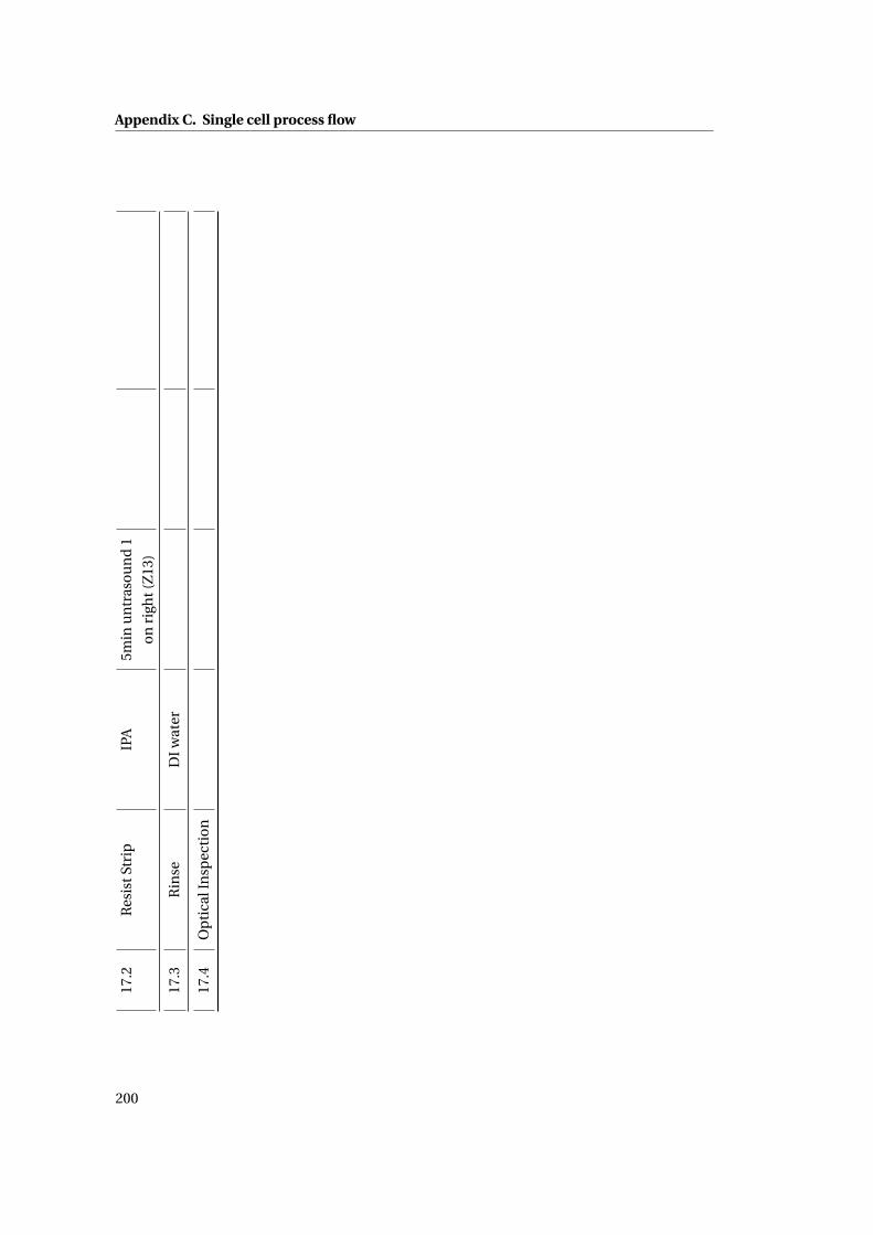
Appendix C. Single cell process flow17
.2R
esis
tStr
ipIP
A5m
inu
ntr
asou
nd
1
on
righ
t(Z
13)
17.3
Rin
seD
Iw
ater
17.4
Op
tica
lIn
spec
tio
n
200

Bibliography
[1] [Online]. Available: http://www.computerhistory.org/timeline/memory-storage/
[2] [Online]. Available: http://www.computerhistory.org/timeline/memory-storage/
[3] G. Potter, J. Mendelson, and S. Sirkin, “Integrated scratchpads sire new generation of
computers,” Electronics, vol. 39, pp. 118–126, 1966.
[4] K. Prall, “Metrics for emerging memories,” in Advances in ReRAM: Materials and Inter-
faces, 2015.
[5] [Online]. Available: http://chipworksrealchips.blogspot.ch/2014/02/
intels-e-dram-shows-up-in-wild.html
[6] R. F. Freitas and W. W. Wilcke, “Storage-class memory: The next storage system technol-
ogy,” IBM Journal of Research and Development, 2008.
[7] IEEE International Solid-States Circuits Conference Tech Trends, 2017.
[8] S. Raoux, J. L. Jordan-Sweet, and A. J. Kellock, “Crystallization properties of ultrathin
phase change films,” Journal of Applied Physics, vol. 103, no. 11, 2008.
[9] S. Privitera, G. Bersuker, B. Butcher, A. Kalantarian, S. Lombardo, C. Bongiorno, R. Geer,
D. Gilmer, and P. Kirsch, “Microscopy study of the conductive filament in hfo 2 resistive
switching memory devices,” Microelectronic Engineering, vol. 109, pp. 75–78, 2013.
[10] B.Govoreanu, G.S.Kar, Y-Y.Chen, V.Paraschiv, S. Kubicek, A.Fantini, I.P.Radu, L.Goux,
S.Clima, R.Degraeve, N.Jossart, O.Richard, T.Vandeweyer, K.Seo, P.Hendrickx, G. Pour-
tois, H.Bender, L.Altimime, D.J.Wouters, J.A.Kittl, and M.Jurczak, “10x10nm2 hf/hfox
crossbar resistive ram with excellent performance, reliability and low-energy operation,”
in International Electron Devices Meeting, 2011, pp. 729–732.
[11] J.-H. Park, Y. Kim, W. Lim, J. Kim, S. Park, W. Kim, K. Kim, J. Jeong, K. Kim, H. Kim
et al., “Enhancement of data retention and write current scaling for sub-20nm stt-mram
by utilizing dual interfaces for perpendicular magnetic anisotropy,” VLSI Technology
(VLSIT), 2012 Symposium on, pp. 57–58, 2012.
201
Bibliography
[12] S. Yu, “Resistive random access memory (rram),” Synthesis Lectures on Emerging Engi-
neering Technologies, vol. 2, no. 5, pp. 1–79, 2016.
[13] T. Hickmott, “Low-frequency negative resistance in thin anodic oxide films,” Journal of
Applied Physics, vol. 33, no. 9, pp. 2669–2682, 1962.
[14] A. Asamitsu, Y. Tomioka, H. Kuwahara, and Y. Tokura, “Current switching of resistive
states in magnetoresistive manganites,” Nature, vol. 388, no. 6637, pp. 50–52, 1997.
[15] A. Beck, J. Bednorz, C. Gerber, C. Rossel, and D. Widmer, “Reproducible switching effect
in thin oxide films for memory applications,” Applied Physics Letters, vol. 77, no. 1, pp.
139–141, 2000.
[16] Y. Watanabe, J. Bednorz, A. Bietsch, C. Gerber, D. Widmer, A. Beck, and S. Wind, “Current-
driven insulator–conductor transition and nonvolatile memory in chromium-doped
srtio 3 single crystals,” Applied Physics Letters, vol. 78, no. 23, pp. 3738–3740, 2001.
[17] I. Baek, M. Lee, S. Seo, M. Lee, D. Seo, D.-S. Suh, J. Park, S. Park, H. Kim, I. Yoo et al.,
“Highly scalable nonvolatile resistive memory using simple binary oxide driven by asym-
metric unipolar voltage pulses,” in Electron Devices Meeting, 2004. IEDM Technical
Digest. IEEE International. IEEE, 2004, pp. 587–590.
[18] S. Seo, M. Lee, D. Seo, E. Jeoung, D.-S. Suh, Y. Joung, I. Yoo, I. Hwang, S. Kim, I. Byun
et al., “Reproducible resistance switching in polycrystalline nio films,” Applied Physics
Letters, vol. 85, no. 23, pp. 5655–5657, 2004.
[19] B. Choi, D. Jeong, S. Kim, C. Rohde, S. Choi, J. Oh, H. Kim, C. Hwang, K. Szot, R. Waser
et al., “Resistive switching mechanism of tio 2 thin films grown by atomic-layer deposi-
tion,” Journal of Applied Physics, vol. 98, no. 3, p. 033715, 2005.
[20] A. Chen, S. Haddad, Y.-C. Wu, T.-N. Fang, Z. Lan, S. Avanzino, S. Pangrle, M. Buynoski,
M. Rathor, W. Cai et al., “Non-volatile resistive switching for advanced memory appli-
cations,” in Electron Devices Meeting, 2005. IEDM Technical Digest. IEEE International.
IEEE, 2005, pp. 746–749.
[21] C.-Y. Lin, C.-Y. Wu, C.-Y. Wu, T.-Y. Tseng, and C. Hu, “Modified resistive switching
behavior of zr o 2 memory films based on the interface layer formed by using ti top
electrode,” Journal of Applied Physics, vol. 102, no. 9, p. 094101, 2007.
[22] N. Xu, L. Liu, X. Sun, X. Liu, D. Han, Y. Wang, R. Han, J. Kang, and B. Yu, “Characteristics
and mechanism of conduction/set process in ti n/ zn o/ pt resistance switching random-
access memories,” Applied Physics Letters, vol. 92, no. 23, p. 232112, 2008.
[23] H. Lee, P. Chen, T. Wu, Y. Chen, C. Wang, P. Tzeng, C. Lin, F. Chen, C. Lien, and M.-J. Tsai,
“Low power and high speed bipolar switching with a thin reactive ti buffer layer in robust
hfo2 based rram,” in Electron Devices Meeting, 2008. IEDM 2008. IEEE International.
IEEE, 2008, pp. 1–4.
202
Bibliography
[24] Z. Wei, Y. Kanzawa, K. Arita, Y. Katoh, K. Kawai, S. Muraoka, S. Mitani, S. Fujii,
K. Katayama, M. Iijima et al., “Highly reliable taox reram and direct evidence of redox
reaction mechanism,” in Electron Devices Meeting, 2008. IEDM 2008. IEEE International.
IEEE, 2008, pp. 1–4.
[25] W. Kim, S. I. Park, Z. Zhang, Y. Yang-Liauw, D. Sekar, H.-S. P. Wong, and S. S. Wong,
“Forming-free nitrogen-doped alo x rram with sub-μa programming current,” in VLSI
Technology (VLSIT), 2011 Symposium on. IEEE, 2011, pp. 22–23.
[26] D. B. Strukov, G. S. Snider, D. R. Stewart, and R. S. Williams, “The missing memristor
found,” nature, vol. 453, no. 7191, pp. 80–83, 2008.
[27] L. Chua, “Memristor-the missing circuit element,” IEEE Transactions on circuit theory,
vol. 18, no. 5, pp. 507–519, 1971.
[28] H.-S. P. Wong, C. Ahn, J. Cao, H.-Y. Chen, S. B. Eryilmaz, S. W. Fong, J. A. Incorvia, Z. Jiang,
H. Li, C. Neumann, K. Okabe, S. Qin, J. Sohn, Y. Wu, and X. Z. S. Yu. Stanford memory
trends. [Online]. Available: https://nano.stanford.edu/stanford-memory-trends
[29] S. Yu and P.-Y. Chen, “Emerging memory technologies,” IEEE Solid-State Circuits Maga-
zine, pp. 43–56, 2016.
[30] I. Valov, R. Waser, J. R. Jameson, and M. N. Kozicki, “Electrochemical metallization
memories—fundamentals, applications, prospects,” Nanotechnology, vol. 22, no. 25, p.
254003, 2011.
[31] S. Yu, X. Guan, and H.-S. P. Wong, “Conduction mechanism of tin/hfox/pt resistive
switching memory: A trap-assisted-tunneling model,” Applied Physics Letters, vol. 99,
no. 6, p. 063507, 2011.
[32] S. Yu, R. Jeyasingh, Y. Wu, and H.-S. P. Wong, “Characterization of low-frequency noise
in the resistive switching of transition metal oxide hfo 2,” Physical Review B, vol. 85,
no. 4, p. 045324, 2012.
[33] G. Bersuker, D. Gilmer, D. Veksler, P. Kirsch, L. Vandelli, A. Padovani, L. Larcher,
K. McKenna, A. Shluger, V. Iglesias et al., “Metal oxide resistive memory switching
mechanism based on conductive filament properties,” Journal of Applied Physics, vol.
110, no. 12, p. 124518, 2011.
[34] S. Yu, R. Jeyasingh, Y. Wu, and H.-S. Philip Wong, “Ac conductance measurement and
analysis of the conduction processes in hfox based resistive switching memory,” Applied
Physics Letters, vol. 99, no. 23, p. 232105, 2011.
[35] G. Bersuker, D. Gilmer, D. Veksler, J. Yum, H. Park, S. Lian, L. Vandelli, A. Padovani,
L. Larcher, K. McKenna et al., “Metal oxide rram switching mechanism based on conduc-
tive filament microscopic properties,” in Electron Devices Meeting (IEDM), 2010 IEEE
International. IEEE, 2010, pp. 19–6.
203
Bibliography
[36] A. Padovani, L. Larcher, O. Pirrotta, L. Vandelli, and G. Bersuker, “Microscopic modeling
of hfo x rram operations: From forming to switching,” IEEE Transactions on electron
devices, vol. 62, no. 6, pp. 1998–2006, 2015.
[37] S. Yu, X. Guan, and H.-S. P. Wong, “Understanding metal oxide rram current overshoot
and reliability using kinetic monte carlo simulation,” in Electron Devices Meeting (IEDM),
2012 IEEE International. IEEE, 2012, pp. 26–1.
[38] H.-S. P. Wong, H.-Y. Lee, S. Yu, Y.-S. Chen, Y. Wu, P.-S. Chen, B. Lee, F. T. Chen, and M.-J.
Tsai, “Metal–oxide rram,” Proceedings of the IEEE, vol. 100, no. 6, pp. 1951–1970, 2012.
[39] X. Guan, S. Yu, and H.-S. P. Wong, “A spice compact model of metal oxide resistive
switching memory with variations,” IEEE electron device letters, vol. 33, no. 10, pp.
1405–1407, 2012.
[40] P. Huang, X. Y. Liu, B. Chen, H. T. Li, Y. J. Wang, Y. X. Deng, K. L. Wei, L. Zeng, B. Gao,
G. Du et al., “A physics-based compact model of metal-oxide-based rram dc and ac
operations,” IEEE Trans. Electron Devices, vol. 60, no. 12, pp. 4090–4097, 2013.
[41] M. Bocquet, D. Deleruyelle, H. Aziza, C. Muller, J.-M. Portal, T. Cabout, and E. Jalaguier,
“Robust compact model for bipolar oxide-based resistive switching memories,” IEEE
Transactions on Electron Devices, vol. 61, no. 3, pp. 674–681, 2014.
[42] L. Larcher, F. M. Puglisi, P. Pavan, A. Padovani, L. Vandelli, and G. Bersuker, “A compact
model of program window in hfo x rram devices for conductive filament characteristics
analysis,” IEEE Transactions on Electron Devices, vol. 61, no. 8, pp. 2668–2673, 2014.
[43] I. Valov, S. Tappertzhofen, E. Linn, and R. Waser, “(invited) the role of electrochemical
interfaces in reram memory cells,” ECS Transactions, vol. 58, no. 7, pp. 189–196, 2013.
[44] U. Schmid, “The impact of thermal annealing and adhesion film thickness on the
resistivity and the agglomeration behavior of titanium/platinum thin films,” Journal of
Applied Physics, vol. 103, no. 5, p. 054902, 2008.
[45] [Online]. Available: https://cmi.epfl.ch/
[46] [Online]. Available: http://www.imicromaterials.com/technical/
reflectivity-control-in-lithography
[47] J. Shoeb and M. J. Kushner, “Mechanisms for plasma etching of hfo 2 gate stacks with
si selectivity and photoresist trimming,” Journal of Vacuum Science & Technology A:
Vacuum, Surfaces, and Films, vol. 27, no. 6, pp. 1289–1302, 2009.
[48] P. Rai-Choudhury, Handbook of microlithography, micromachining, and microfabrica-
tion: microlithography. Iet, 1997, vol. 1.
204
Bibliography
[49] M. Darnon, T. Chevolleau, D. Eon, L. Vallier, J. Torres, and O. Joubert, “Etching charac-
teristics of tin used as hard mask in dielectric etch process,” Journal of Vacuum Science
& Technology B: Microelectronics and Nanometer Structures Processing, Measurement,
and Phenomena, vol. 24, no. 5, pp. 2262–2270, 2006.
[50] J. Tonotani, T. Iwamoto, F. Sato, K. Hattori, S. Ohmi, and H. Iwai, “Dry etching character-
istics of tin film using ar/chf 3, ar/cl 2, and ar/bcl 3 gas chemistries in an inductively
coupled plasma,” Journal of Vacuum Science & Technology B: Microelectronics and
Nanometer Structures Processing, Measurement, and Phenomena, vol. 21, no. 5, pp.
2163–2168, 2003.
[51] D.-P. Kim, X. Yang, J.-C. Woo, D.-S. Um, and C.-I. Kim, “Dry-etching properties of tin
for metal/high-k gate stack using b cl 3-based inductively coupled plasma a,” Journal
of Vacuum Science & Technology A: Vacuum, Surfaces, and Films, vol. 27, no. 6, pp.
1320–1325, 2009.
[52] E. Sungauer, E. Pargon, X. Mellhaoui, R. Ramos, G. Cunge, L. Vallier, O. Joubert, and
T. Lill, “Etching mechanisms of hf o 2, si o 2, and poly-si substrates in b cl 3 plasmas,”
Journal of Vacuum Science & Technology B: Microelectronics and Nanometer Structures
Processing, Measurement, and Phenomena, vol. 25, no. 5, pp. 1640–1646, 2007.
[53] S. A. Vitale, J. Kedzierski, and C. L. Keast, “High density plasma etching of titanium
nitride metal gate electrodes for fully depleted silicon-on-insulator subthreshold tran-
sistor integration,” Journal of Vacuum Science & Technology B: Microelectronics and
Nanometer Structures Processing, Measurement, and Phenomena, vol. 27, no. 6, pp.
2472–2479, 2009.
[54] H. Shin, W. Zhu, L. Liu, S. Sridhar, V. M. Donnelly, D. J. Economou, C. Lenox, and T. Lii,
“Selective etching of tin over tan and vice versa in chlorine-containing plasmas,” Journal
of Vacuum Science & Technology A: Vacuum, Surfaces, and Films, vol. 31, no. 3, p. 031305,
2013.
[55] K. Nojiri, Dry etching technology for semiconductors. Springer, 2014.
[56] S. Tabara, “Notch profile defect in aluminum alloy etching using high-density plasma,”
Japanese journal of applied physics, vol. 35, no. 4S, p. 2456, 1996.
[57] S. Logothetidis, E. Meletis, G. Stergioudis, and A. Adjaottor, “Room temperature oxida-
tion behavior of tin thin films,” Thin Solid Films, vol. 338, no. 1, pp. 304–313, 1999.
[58] L. Broussous, D. Krejcirova, K. Courouble, S. Zoll, A. Iwasaki, H. Ishikawa, F. Buisine,
A. Lamaury, and D. Fuard, “Tin hard mask cleans with sc1 solutions, for 64nm pitch beol
patterning,” in Solid State Phenomena, vol. 219. Trans Tech Publ, 2015, pp. 209–212.
[59] D. Triyoso, R. Liu, D. Roan, M. Ramon, N. Edwards, R. Gregory, D. Werho, J. Kulik,
G. Tam, E. Irwin et al., “Impact of deposition and annealing temperature on material
205
Bibliography
and electrical characteristics of ald hfo2,” Journal of The Electrochemical Society, vol.
151, no. 10, pp. F220–F227, 2004.
[60] H. Kim, P. C. McIntyre, and K. C. Saraswat, “Effects of crystallization on the electrical
properties of ultrathin hfo 2 dielectrics grown by atomic layer deposition,” Applied
physics letters, vol. 82, no. 1, pp. 106–108, 2003.
[61] M. Seo, S. K. Kim, K.-M. Kim, T. Park, J. H. Kim, C. S. Hwang, and H. J. Cho, “Crystalliza-
tion and wet etching characteristics of atomic layer deposited hfo2 films using hf ([n
(ch3)(c2h5)] 3 [oc (ch3) 3]) precursor and o3 oxidant,” ECS Transactions, vol. 1, no. 5, pp.
211–217, 2006.
[62] M. Zervas, “High throughput screening platform for ultra large scale integration based
on high-k silicon nanowire isfet and 3d integration,” 2013.
[63] H. Wan, P. Zhou, L. Ye, Y. Lin, T. Tang, H. Wu, and M. Chi, “In situ observation of
compliance-current overshoot and its effect on resistive switching,” IEEE Electron Device
Letters, vol. 31, no. 3, pp. 246–248, 2010.
[64] K. Beckmann, J. Holt, W. Olin-Ammentorp, Z. Alamgir, J. Van Nostrand, and N. C. Cady,
“The effect of reactive ion etch (rie) process conditions on reram device performance,”
Semiconductor Science and Technology, 2017.
[65] J. Sandrini, B. Attarimashalkoubeh, E. Shahrabi, I. Krawczuk, and Y. Leblebici, “Effect of
metal buffer layer and thermal annealing on hfo x-based rerams,” in Science of Electrical
Engineering (ICSEE), IEEE International Conference on the. Ieee, 2016, pp. 1–5.
[66] B. Attarimashalkoubeh, J. Sandrini, E. Shahrabi, M. Barlas, and Y. Leblebici, “Effect of
hf metal layer on the switching characteristic of hfox-based resistive random access
memory,” in Ph. D. Research in Microelectronics and Electronics (PRIME), 2016 12th
Conference on. Ieee, 2016, pp. 1–4.
[67] N. Srinivasan, K. Rook, I. Berry, B. Rubin, and F. Cerio, “Ion beam etch for patterning of
resistive ram (reram) devices,” MRS Advances, vol. 2, no. 4, pp. 247–252, 2017.
[68] A. Chen, “Area and thickness scaling of forming voltage of resistive switching memories,”
IEEE Electron Device Letters, vol. 35, no. 1, pp. 57–59, 2014.
[69] J. Kim, K. Jung, Y. Kim, Y. Jo, S. Cho, H. Woo, S. Lee, A. I. Inamdar, J. Hong, J.-K. Lee, H. Kim,
and H. Im, “Switching power universality in unipolar resistive switching memories,”
Nature Scientific Reports, vol. 6, 2016.
[70] G. Ghosh and M. K. Orlowski, “Correlation between set and reset voltages in resistive
ram cells,” Current Applied Physics, pp. 1124–1129, 2015.
[71] S. Larentis, F. Nardi, S. Balatti, D. C. Gilmer, and D. Ielmini, “Resistive switching by
voltage-driven ion migration in bipolar rram—part ii: Modeling,” IEEE Transactions on
Electron Devices, vol. 59, no. 9, pp. 2468–2475, 2012.
206
Bibliography
[72] J. Sandrini, E. Shahrabi, B. Attarimashalkoubeh, and Y. Leblebici, “Statistical correlation
between forming, set, reset, lrs and hrs in oxide-based rerams,” IEEE Transactions on
Nanotechnology, submitted.
[73] Y.-S. Chen, H.-Y. Lee, P.-S. Chen, T.-Y. Wu, C.-C. Wang, P.-J. Tzeng, F. Chen, M.-J. Tsai,
and C. Lien, “An ultrathin forming-free hfox resistance memory with excellent electrical
performance,” IEEE Electron Device Letters, pp. 1473 – 1475, 2010.
[74] Y. Liu, Z. Wang, A. Lee, F. Su, C.-P. Lo, Z. Yuan, C.-C. Lin, Q. Wei, Y. Wang, Y.-C. King et al.,
“4.7 a 65nm reram-enabled nonvolatile processor with 6× reduction in restore time and
4× higher clock frequency using adaptive data retention and self-write-termination
nonvolatile logic,” in Solid-State Circuits Conference (ISSCC), 2016 IEEE International.
IEEE, 2016, pp. 84–86.
[75] R. Fackenthal, M. Kitagawa, W. Otsuka, K. Prall, D. Mills, K. Tsutsui, J. Javanifard,
K. Tedrow, T. Tsushima, Y. Shibahara et al., “19.7 a 16gb reram with 200mb/s write
and 1gb/s read in 27nm technology,” in Solid-State Circuits Conference Digest of Techni-
cal Papers (ISSCC), 2014 IEEE International. IEEE, 2014, pp. 338–339.
[76] M.-F. Chang, J.-J. Wu, T.-F. Chien, Y.-C. Liu, T.-C. Yang, W.-C. Shen, Y.-C. King, C.-J. Lin,
K.-F. Lin, Y.-D. Chih et al., “19.4 embedded 1mb reram in 28nm cmos with 0.27-to-1v
read using swing-sample-and-couple sense amplifier and self-boost-write-termination
scheme,” in Solid-State Circuits Conference Digest of Technical Papers (ISSCC), 2014 IEEE
International. IEEE, 2014, pp. 332–333.
[77] A. Kawahara, R. Azuma, Y. Ikeda, K. Kawai, Y. Katoh, Y. Hayakawa, K. Tsuji, S. Yoneda,
A. Himeno, K. Shimakawa et al., “An 8 mb multi-layered cross-point reram macro with
443 mb/s write throughput,” IEEE Journal of Solid-State Circuits, vol. 48, no. 1, pp.
178–185, 2013.
[78] M.-F. Chang, C.-W. Wu, C.-C. Kuo, S.-J. Shen, K.-F. Lin, S.-M. Yang, Y.-C. King, C.-J. Lin,
and Y.-D. Chih, “A 0.5 v 4mb logic-process compatible embedded resistive ram (reram)
in 65nm cmos using low-voltage current-mode sensing scheme with 45ns random read
time,” in Solid-State Circuits Conference Digest of Technical Papers (ISSCC), 2012 IEEE
International. IEEE, 2012, pp. 434–436.
[79] J. Yi, H. Choi, S. Song, D. Son, S. Lee, J. Park, W. Kim, M. Sung, S. Lee, J. Moon, C. Kim,
J. Park, M. Joo, J. Roh, S. Park, S.-W. Chung, J. Jeong, S.-J. Hong, and S.-W. Park, “Re-
quirements of bipolar switching reram for 1t1r type high density memory array,” in IEEE
International Symposium on VLSI Technology, Systems and Applications, 2011, pp. 1–2.
[80] I. G. Baek, C. J. Park, H. Ju, D. J. Seong, H. S. Ahn, J. H. Kim, M. K. Yang, S. H. Song, E. M.
Kim, S. O. Park, C. H. Park, C. W. Song, G. T. Jeong, S. Choi, H. K. Kang, and C. Chung,
“Realization of vertical resistive memory (vrram) using cost effective 3d process,” in IEEE
International Electron Devices Meeting (IEDM), 2011.
207
Bibliography
[81] H. D. Lee, S. G. Kim, K. Cho, H. Hwang, H. Choi, J. Lee, S. H. Lee, H. J. Lee, J. Suh, S.-O.
Chung, Y. S. Kim, K. S. Kim, W. S. Nam, J. T. Cheong, J. T. Kim, S. Chae, E.-R. Hwang,
S. N. Park, Y. S. Sohn, C. G. Lee, H. S. Shin, K. J. Lee, K. Hong, H. G. Jeong, K. M. Rho,
Y. K. Kim, S. Chung, J.Nickel, J. J. Yang, H. S. Cho, F. Perner, R. S. Williams, J. H. Lee, S. K.
Park, and S.-J. Hong, “Integration of 4f2 selector-less crossbar array 2mb reram based
on transition metal oxides for high density memory applications,” in Symposium on
VLSI Technology, 2012.
[82] J.-J. Huang, Y.-M. Tseng, W.-C. Luo, C.-W. Hsu, and T.-H. Hou, “One selector-one re-
sistor (1s1r) crossbar array for high-density flexible memory applications,” in IEEE
International Electron Devices Meeting (IEDM), 2011, pp. 733–736.
[83] E. Linn, R. Rosezin, C. Kügeler, and R. Waser, “Complementary resistive switches for
passive nanocrossbar memories,” Nature Materials, vol. 9, pp. 403–406, 2010.
[84] A. Kawahara, R. Azuma, Y. Ikeda, K. Kawai, Y. Katoh, Y. Hayakawa, K. Tsuji, S. Yoneda,
A. Himeno, K. Shimakawa, T. Takagi, T. Mikawa, and K. Aono, “An 8 mb multi-layered
cross-point reram macro with 443 mb/s write throughput,” IEEE Journal of Solid-State
Circuits (JSSC), vol. 48, no. 1, pp. 178 – 185, 2013.
[85] J. Sandrini, T. Demirci, M. Thammasack, D. Sacchetto, and Y. Leblebici, “Low-voltage
read/write circuit design for transistorless reram crossbar arrays in 180nm cmos tech-
nology,” in Circuits and Systems (ISCAS), 2015 IEEE International Symposium on. IEEE,
2015, pp. 9–12.
[86] A. Chen, A. Kinoshita, G. Bourianoff, M. Garner, V. Zhirnov, and J. Hutchby, “Emerging
memory select device workshop,” ITRS Emerging Research Device Report, Tech. Rep.,
2012.
[87] M. J. Kanga, T. J. Parka, Y. W. Kwon, D. H. Ahnb, Y. S. Kanga, H. Jeonga, S. J. Ahna, Y. J.
Songa, B. C. Kima, S. Namb, H. K. Kangb, G. T. Jeonga, and C. H. Chung, “Pram cell
technology and characterization in 20nm node size,” in IEEE International Electron
Devices Meeting (IEDM), 2011.
[88] Y. Sasago, M. Kinoshita, T. Morikawa, K. Kurotsuchi, S. Hanzawa, T. Mine, A. Shima,
Y. Fujisaki, H. Kume, H. Moriya, N. Takaura, and K. Torii, “Cross-point phase change
memory with 4f2 cell size driven by cross-point phase change memory with 4f2 cell
size driven by low-contact-resistivity poly-si diode,” in Symposium on VLSI Technology
Digest of Technical Papers, 2009.
[89] M.-J. Lee, Y. Park, B.-S. Kang, S.-E. Ahn, C. Lee, K. Kim, W. Xianyu, G. Stefanovich,
Jung-HyunLee, Seok-JaeChung, Y.-H. Kim, Chang-SooLe, J.-B. P. , In-GyuBaek, and
In-KyeongYoo, “2-stack id-ir cross-point structure with oxide diodes as switch elements
for high density resistance ram applications,” in IEEE International Electron Devices
Meeting (IEDM), 2007.
208
Bibliography
[90] A. Kawahara, R. Azuma, Y. Ikeda, K. Kawai, Y. Katoh, K. Tanabe, T. Nakamura, Y. Sumi-
moto, N. Yamada, N. Nakai, S. Sakamoto, Y. Hayakawa, K. Tsuji, S. Yoneda, A. Himeno,
K. ichi Origasa, K. Shimakawa, T. Takagi, T. Mikawa, and K. Aono, “An 8mb multi-layered
cross-point reram macro with 443mb/s write throughput,” in International Solid-State
Circuits Conference (ISSCC), 2012.
[91] M. Son, J. Lee, J. Park, J. Shin, G. Choi, S. Jung, W. Lee, S. Kim, S. Park, and H. Hwang,
“Excellent selector characteristics of nanoscale vo2 for high-density bipolar reram appli-
cations,” IEEE Electron Device Letters, vol. 32, no. 11, pp. 1579–1581, 2011.
[92] K. Gopalakrishnan, R. S. Shenoy, C. T. Rettner, K. Virwani, D. S. Bethune, R. M. Shelby,
G. W. Burr, A. Kellock, R. S. King, K. Nguyen, A. N. Bowers, M. Jurich, B. Jackson, A. M.
Friz, T. Topuria, P. M. Rice, and B. N. Kurdi, “Highly-scalable novel access device based
on mixed ionic electronic conduction (miec) materials for high density phase change
memory (pcm) arrays,” in Symposium on VLSI Technology Digest of Technical Papers,
2010.
[93] H.-W. Ahn, D. S. J. andByung-ki Cheong, S. dong Kim, S.-Y. Shin, H. Lim, D. Kim, and
S. Leea, “A study on the scalability of a selector device using threshold switching in
pt/gese/pt,” in ECS Solid State Letters, 2013.
[94] K. Zhang, B. Wang, F. Wang, Y. Han, X. Jian, H. Zhang, and H. P. Wong, “Vo 2-based
selection device for passive resistive random access memory application,” IEEE Electron
Device Letters, vol. 37, no. 8, pp. 978–981, 2016.
[95] M.-H. Lee, M.-G. Kim, and H.-K. Song, “Thermochromism of rapid thermal annealed vo
2 and sn-doped vo 2 thin films,” Thin Solid Films, vol. 290, pp. 30–33, 1996.
[96] A. Paone, “Switchable selective absorber coatings for overheating protection of solar
thermal collectors,” 2013.
[97] J. B. Goodenough, “The two components of the crystallographic transition in vo2,”
Journal of Solid State Chemistry, vol. 3, no. 4, pp. 490–500, 1971.
[98] J. Sandrini, A. Cevrero, T. Demirci, P.-E. Gaillardon, D. Sacchetto, G. De Micheli, and
Y. Leblebici, “Heterogeneous integration of reram crossbars in a cmos foundry chip,” in
Proceedings of the 40th International Micro and Nano Engineering Conference (MNE),
no. EPFL-CONF-201908, 2014.
[99] J. Sandrini, M. Thammasack, T. Demirci, P.-E. Gaillardon, D. Sacchetto, G. De Micheli,
and Y. Leblebici, “Heterogeneous integration of reram crossbars in 180nm cmos beol
process,” Microelectronic Engineering, vol. 145, pp. 62–65, 2015.
[100] J. Sandrini, M. Barlas, M. Thammasack, T. Demirci, M. De Marchi, D. Sacchetto, P.-E.
Gaillardon, G. De Micheli, and Y. Leblebici, “Co-design of reram passive crossbar arrays
integrated in 180 nm cmos technology,” IEEE Journal on Emerging and Selected Topics
in Circuits and Systems, vol. 6, no. 3, pp. 339–351, 2016.
209

Bibliography
[101] K. Buchanan, “The evolution of interconnect technology for silicon integrated circuitry,”
in Proc. of International conference on compound semiconductor manufacturing GaAs-
MANTECH2002, vol. 15, 2002, pp. 50–52.
[102] S. Yu, X. Guan, and H.-S. P. Wong, “On the switching parameter variation of metal oxide
rram—part ii: Model corroboration and device design strategy,” IEEE Transactions on
Electron Devices, vol. 59, no. 4, pp. 1183–1188, April 2012.
210


Publications
[1] J. Sandrini, E. Shahrabi, B. Attarimashalkoubeh, and Y. Leblebici, “Statistical correlation
between forming, set, reset, lrs and hrs in oxide-based rerams,” IEEE Transactions on
Nanotechnology, submitted.
[2] B. Attarimashalkoubeh, J. Sandrini, E. Shahrabi, and Y. Leblebici, “Evolution of oxygen
vacancies under electrical characterization for hfox-based rerams,” in European Solid-
State Device Research Conference (ESSDERC), 2017.
[3] M. Pezzarossa, J. Sandrini, E. Shahrabi, B. Attarimashalkoubeh, and Y. Leblebici, “Cell
area and buffer layer thickness effects on hfox-based rerams,” in Proceedings of the 40th
International Micro and Nano Engineering Conference (MNE), 2017.
[4] E. Shahrabi, B. Attarimashalkoubeh, J. Sandrini, and Y. Leblebici, “Towards chip-level
reram-cmos co-integration,” in International Conference on Memristive Materials, Devices
and Systems (MEMRYSIS), April 2017.
[5] B. Attarimashalkoubeh, J. Sandrini, E. Shahrabi, and Y. Leblebici, “Effect of electrical
measurements on the evolution of conductive filaments composed of oxygen vacancies
in hfox-based reram,” in International Conference on Memristive Materials, Devices and
Systems (MEMRYSIS), April 2017.
[6] J. Sandrini, E. Shahrabi, B. Attarimashalkoubeh, and Y. Leblebici, “Correlation analysis be-
tween set, reset, forming, lrs and hrs in oxide-based rerams,” in International Conference
on Memristive Materials, Devices and Systems (MEMRYSIS), April 2017.
[7] J. Tranchant, J. Sandrini, E. Janod, D. Sacchetto, B. Corraze, M.-P. Besland, J. Ghanbaja,
G. De Micheli, P.-E. Gaillardon, and L. Cario, “Control of resistive switching in mott
memories based on tin/am4q8/tin mim devices,” ECS Transactions, vol. 75, no. 32, pp.
3–12, 2017.
[8] J. Sandrini, B. Attarimashalkoubeh, E. Shahrabi, I. Krawczuk, and Y. Leblebici, “Effect of
metal buffer layer and thermal annealing on hfo x-based rerams,” in Science of Electrical
Engineering (ICSEE), IEEE International Conference on the. Ieee, 2016, pp. 1–5.
[9] B. Attarimashalkoubeh, J. Sandrini, E. Shahrabi, M. Barlas, and Y. Leblebici, “Effect of
hf metal layer on the switching characteristic of hfox-based resistive random access
Publications
memory,” in Ph. D. Research in Microelectronics and Electronics (PRIME), 2016 12th
Conference on. Ieee, 2016, pp. 1–4.
[10] J. Sandrini, M. Barlas, M. Thammasack, T. Demirci, M. De Marchi, D. Sacchetto, P.-E.
Gaillardon, G. De Micheli, and Y. Leblebici, “Co-design of reram passive crossbar arrays
integrated in 180 nm cmos technology,” IEEE Journal on Emerging and Selected Topics in
Circuits and Systems, vol. 6, no. 3, pp. 339–351, 2016.
[11] E. Shahrabi, J. Sandrini, B. Attarimashalkoubeh, T. Demirci, M. Hadad, and Y. Leblebici,
“Chip-level cmos co-integration of reram-based non-volatile memories,” in Ph. D. Re-
search in Microelectronics and Electronics (PRIME), 2016 12th Conference on. Ieee, 2016,
pp. 1–4.
[12] I. Boybat, J. Sandrini, D. Sacchetto, G. W. Burr, and Y. Leblebici, “Cognitive computing
with non-volatile memory elements,” in MemoCIS Training School, May 2015.
[13] J. Sandrini, T. Demirci, M. Thammasack, D. Sacchetto, and Y. Leblebici, “Low-voltage
read/write circuit design for transistorless reram crossbar arrays in 180nm cmos tech-
nology,” in Circuits and Systems (ISCAS), 2015 IEEE International Symposium on. IEEE,
2015, pp. 9–12.
[14] J. Sandrini, M. Thammasack, T. Demirci, P.-E. Gaillardon, D. Sacchetto, G. De Micheli,
and Y. Leblebici, “Heterogeneous integration of reram crossbars in 180nm cmos beol
process,” Microelectronic Engineering, vol. 145, pp. 62–65, 2015.
[15] P.-E. Gaillardon, X. Tang, J. Sandrini, M. Thammasack, S. R. Omam, D. Sacchetto,
Y. Leblebici, and G. De Micheli, “A ultra-low-power fpga based on monolithically inte-
grated rrams,” in Proceedings of the 2015 Design, Automation & Test in Europe Conference
& Exhibition. EDA Consortium, 2015, pp. 1203–1208.
[16] J. Sandrini, A. Cevrero, T. Demirci, P.-E. Gaillardon, D. Sacchetto, G. De Micheli, and
Y. Leblebici, “Heterogeneous integration of reram crossbars in a cmos foundry chip,” in
Proceedings of the 40th International Micro and Nano Engineering Conference (MNE), no.
EPFL-CONF-201908, 2014.
[17] S. Raoux, H.-Y. Cheng, J. Sandrini, J. Li, and J. Jordan-Sweet, “Materials engineering for
phase change random access memory,” in Non-Volatile Memory Technology Symposium
(NVMTS), 2011 11th Annual. IEEE, 2011, pp. 1–5.

Related Documents


