Extending Synchronization from Super-threshold to Sub-threshold Region Jun Zhou, Maryam Ashouei, David Kinniment*, Jos Huisken and Gordon Russell* IMEC Netherlands & *Newcastle University

Welcome message from author
This document is posted to help you gain knowledge. Please leave a comment to let me know what you think about it! Share it to your friends and learn new things together.
Transcript

Extending Synchronization from
Super-threshold to Sub-threshold Region
Jun Zhou, Maryam Ashouei, David Kinniment*, Jos Huisken and Gordon Russell*
IMEC Netherlands & *Newcastle University

• Sub-threshold Operation
• Synchronization in Multi-Low-VDD Systems on Chip
• Low Voltage Synchronizer Design
• Sub-threshold Synchronizer Design
• Results
• Implementation
• Conclusion

• Sub-threshold Operation
• Synchronization in Multi-Low-VDD Systems on Chip
• Low Voltage Synchronizer Design
• Sub-threshold Synchronizer Design
• Results
• Implementation
• Conclusion
� 4© Holst Centre
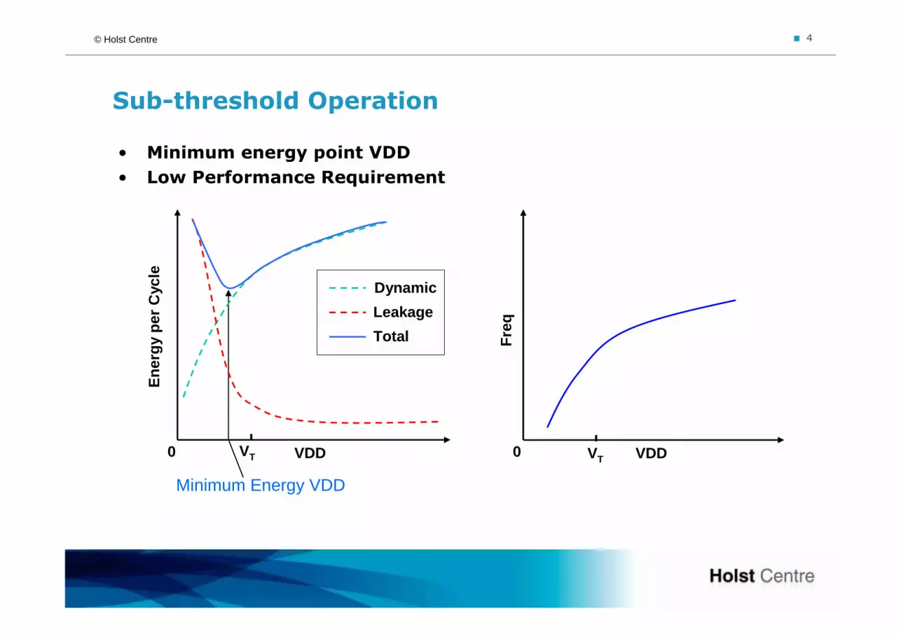
Sub-threshold Operation
• Minimum energy point VDD
• Low Performance Requirement
Minimum Energy VDDF
req
VDD
En
erg
y p
er C
ycle
Dynamic
Leakage
Total
VDD0 0VT VT

• Sub-threshold Operation
• Synchronization in Multi-Low-VDD Systems on Chip
• Low Voltage Synchronizer Design
• Sub-threshold Synchronizer Design
• Results
• Implementation
• Conclusion

� 6© Holst Centre
Multi-Low-VDD Systems on Chip
VDD/Clock Domain A
Norm VDD
VDD/Clock Domain B
Low VDD
VDD/Clock Domain C
Sub-threshold VDD
Network on Chip
S S
S
Synchronizers

• Sub-threshold Operation
• Synchronization in Multi-Low-VDD Systems on Chip
• Low Voltage Synchronizer Design
• Sub-threshold Synchronizer Design
• Results
• Implementation
• Conclusion

� 8© Holst Centre
Synchronizer Performance (MTBF)
dcw
Tt
ffT
eMTBF
ds
τ−
=
ts: Synchronization TimeTd : Normal Propagation Delayτ : Metastability Time Constant Tw : Metastability Windowfc : Clock Frequencyfd : Incoming Data Frequency
In the Super-threshold Region:
�
�
↓↓↑→↓→∝ MTBFTVDDVDDT dd ,
↓↓↑→↓→∝∝∝ MTBFVDDVDDIgandg
Cdm
m
ττ ,2
In the Sub-threshold Region:
�
�
↓↓↓↑↑→↓→∝ MTBFTVDDe
VDDT dVDDd ,
↓↓↓↑↑→↓→∝∝∝ MTBFVDDeIgandg
C VDD
dm
m
ττ ,
� 9© Holst Centre
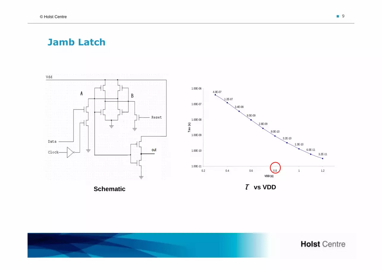
Jamb Latch
τ
9.5E-09
2.8E-09
9.0E-10
3.2E-10
1.3E-10
6.0E-11
3.2E-11
1.2E-07
4.0E-07
3.4E-08
1.00E-11
1.00E-10
1.00E-09
1.00E-08
1.00E-07
1.00E-06
0.2 0.4 0.6 0.8 1 1.2
VDD (v)
Tau
(s)
Schematic vs VDDτ
� 10© Holst Centre
Improved Latch
9.2E-08
8.4E-09
9.8E-10
1.9E-106.6E-11
3.4E-112.1E-11
1.5E-111.2E-11 9.6E-12
1.00E-12
1.00E-11
1.00E-10
1.00E-09
1.00E-08
1.00E-07
1.00E-06
0.2 0.4 0.6 0.8 1 1.2
VDD (v)
Tau
(s)
9.5E-09
2.8E-09
9.0E-10
3.2E-10
1.3E-10
6.0E-11
3.2E-11
1.2E-07
4.0E-07
3.4E-08
1.00E-11
1.00E-10
1.00E-09
1.00E-08
1.00E-07
1.00E-06
0.2 0.4 0.6 0.8 1 1.2
VDD (v)
Tau
(s)
Schematic
vs VDDτ
Jamb Latch
Improved Latch
� 11© Holst Centre
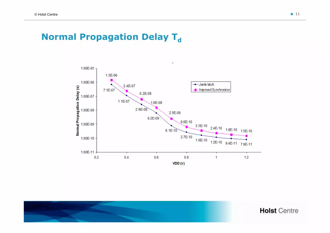
Normal Propagation Delay Td
� 12© Holst Centre
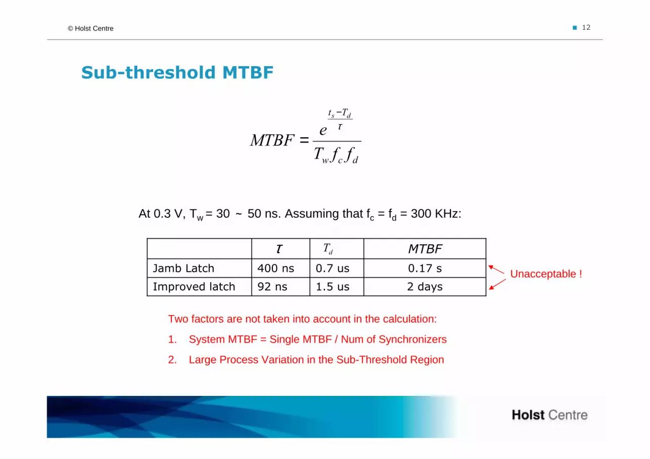
Sub-threshold MTBF
dcw
Tt
ffT
eMTBF
ds
τ−
=
2 days1.5 us92 nsImproved latch
0.17 s0.7 us400 nsJamb Latch
MTBFτ
At 0.3 V, Tw = 30 ~ 50 ns. Assuming that fc = fd = 300 KHz:
dT
Unacceptable !
Two factors are not taken into account in the calculation:
1. System MTBF = Single MTBF / Num of Synchronizers
2. Large Process Variation in the Sub-Threshold Region

� 13© Holst Centre
Process Variation
Mean: 440 nsStd: 230 ns
0
10
20
30
40
50
60
70
80
0 150 300 450 600 750 900 1050 1200 1350 1500 1650 1800
Tau (ns)
Nu
mb
er o
f Occ
ura
nce
Variation of Tau for Jamb Latch at 0.3 V
dcw
Tt
ffT
eMTBF
ds
τ−
=

• Sub-threshold Operation
• Synchronization in Multi-Low-VDD Systems on Chip
• Low Voltage Synchronizer Design
• Sub-threshold Synchronizer Design
• Results
• Implementation
• Conclusion
� 15© Holst Centre
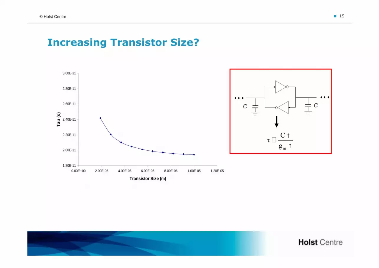
Increasing Transistor Size?
1.80E-11
2.00E-11
2.20E-11
2.40E-11
2.60E-11
2.80E-11
3.00E-11
0.00E+00 2.00E-06 4.00E-06 6.00E-06 8.00E-06 1.00E-05 1.20E-05
Transistor Size (m)
Tau
(s)
↑↑∝
mg
Cτ
� 16© Holst Centre
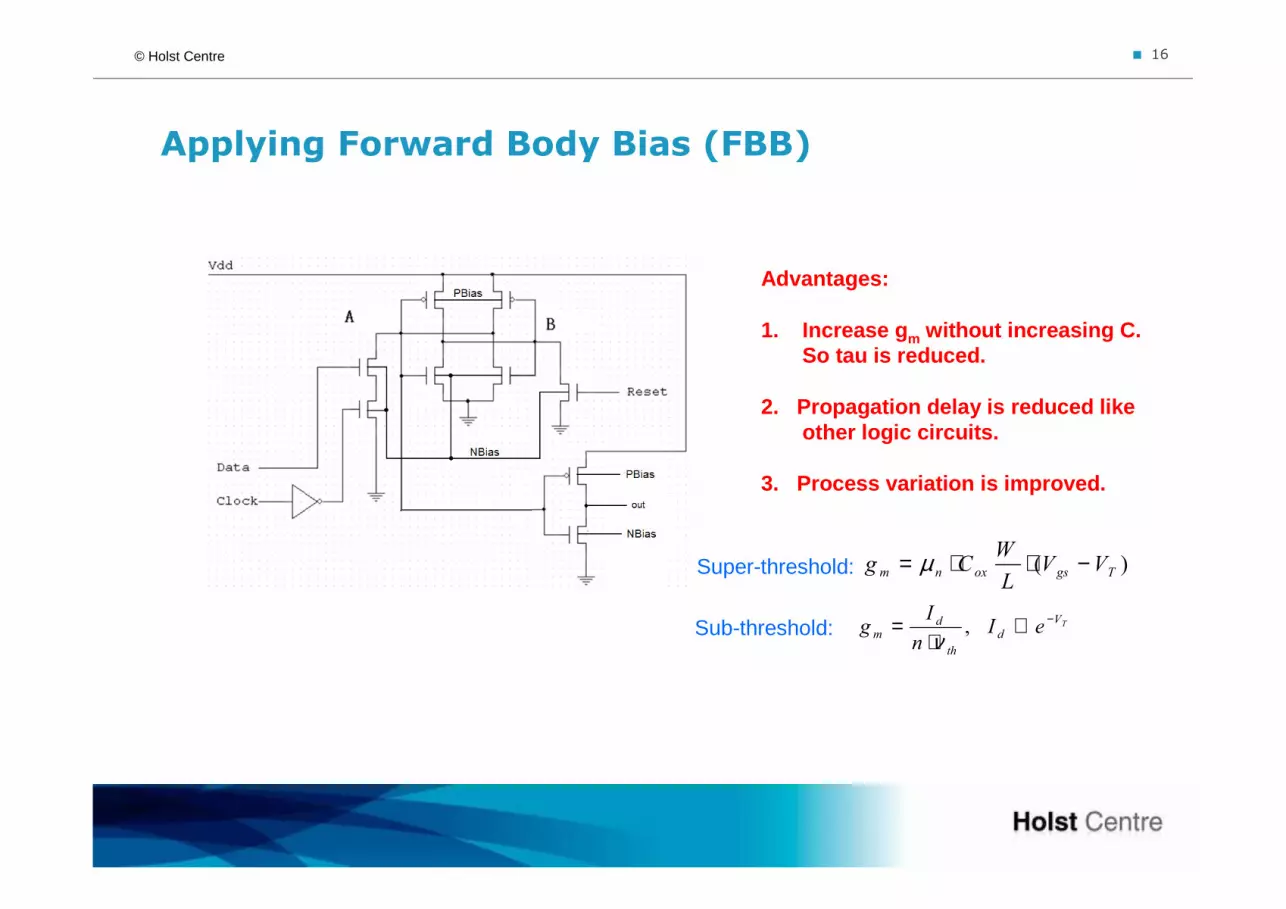
Applying Forward Body Bias (FBB)
Advantages:
1. Increase gm without increasing C. So tau is reduced.
2. Propagation delay is reduced like other logic circuits.
3. Process variation is improved.
)( Tgsoxnm VVL
WCg −⋅⋅= µ
TV
d
th
dm eI
n
Ig
−∝⋅
= ,ν
Super-threshold:
Sub-threshold:

• Sub-threshold Operation
• Synchronization in Multi-Low-VDD Systems on Chip
• Low Voltage Synchronizer Design
• Sub-threshold Synchronizer Design
• Results
• Implementation
• Conclusion
� 18© Holst Centre
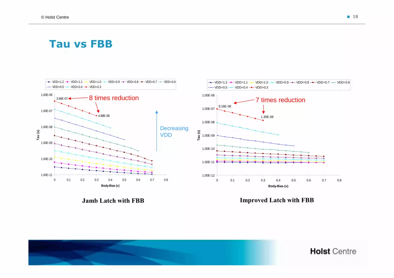
4.88E-08
3.96E-07
1.00E-11
1.00E-10
1.00E-09
1.00E-08
1.00E-07
1.00E-06
0 0.1 0.2 0.3 0.4 0.5 0.6 0.7 0.8
Body-Bias (v)
Tau
(s)
VDD=1.2 VDD=1.1 VDD=1.0 VDD=0.9 VDD=0.8 VDD=0.7 VDD=0.6
VDD=0.5 VDD=0.4 VDD=0.3
Jamb Latch with FBB
Tau vs FBB
1.30E-08
9.16E-08
1.00E-12
1.00E-11
1.00E-10
1.00E-09
1.00E-08
1.00E-07
1.00E-06
0 0.1 0.2 0.3 0.4 0.5 0.6 0.7 0.8
Body-Bias (v)
Tau
(s)
VDD=1.2 VDD=1.1 VDD=1.0 VDD=0.9 VDD=0.8 VDD=0.7 VDD=0.6
VDD=0.5 VDD=0.4 VDD=0.3
Improved Latch with FBB
8 times reduction 7 times reduction
DecreasingVDD
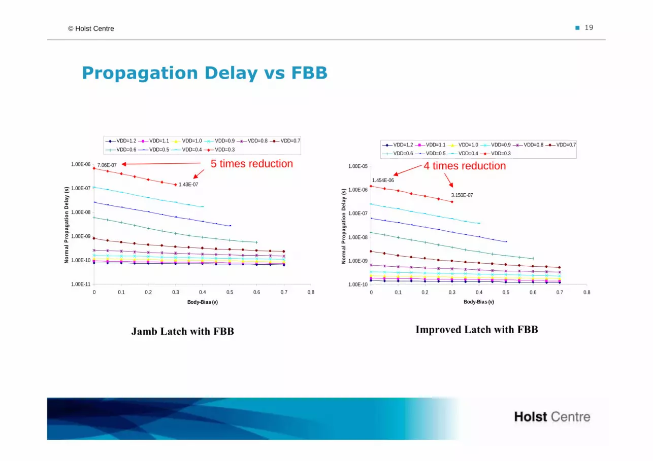
� 19© Holst Centre
3.150E-07
1.454E-06
1.00E-10
1.00E-09
1.00E-08
1.00E-07
1.00E-06
1.00E-05
0 0.1 0.2 0.3 0.4 0.5 0.6 0.7 0.8
Body-Bias (v)
No
rmal
Pro
pag
atio
n D
elay
(s)
VDD=1.2 VDD=1.1 VDD=1.0 VDD=0.9 VDD=0.8 VDD=0.7
VDD=0.6 VDD=0.5 VDD=0.4 VDD=0.3
1.43E-07
7.06E-07
1.00E-11
1.00E-10
1.00E-09
1.00E-08
1.00E-07
1.00E-06
0 0.1 0.2 0.3 0.4 0.5 0.6 0.7 0.8
Body-Bias (v)
No
rmal
Pro
pag
atio
n D
elay
(s)
VDD=1.2 VDD=1.1 VDD=1.0 VDD=0.9 VDD=0.8 VDD=0.7
VDD=0.6 VDD=0.5 VDD=0.4 VDD=0.3
Jamb Latch with FBB
Propagation Delay vs FBB
Improved Latch with FBB
5 times reduction 4 times reduction
� 20© Holst Centre
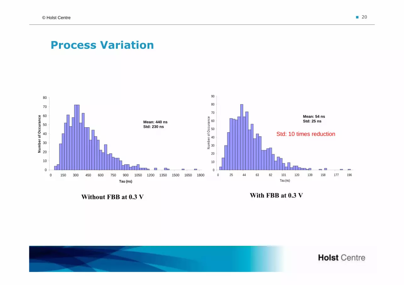
Process Variation
Mean: 440 nsStd: 230 ns
0
10
20
30
40
50
60
70
80
0 150 300 450 600 750 900 1050 1200 1350 1500 1650 1800
Tau (ns)
Nu
mb
er o
f Occ
ura
nce
Mean: 54 nsStd: 25 ns
0
10
20
30
40
50
60
70
80
90
0 25 44 63 82 101 120 139 158 177 196
Tau (ns)
Num
ber o
f Occ
uran
ce
Without FBB at 0.3 V With FBB at 0.3 V
Std: 10 times reduction
Mean: 54 nsStd: 25 nsMean: 440 ns
Std: 230 ns
� 21© Holst Centre
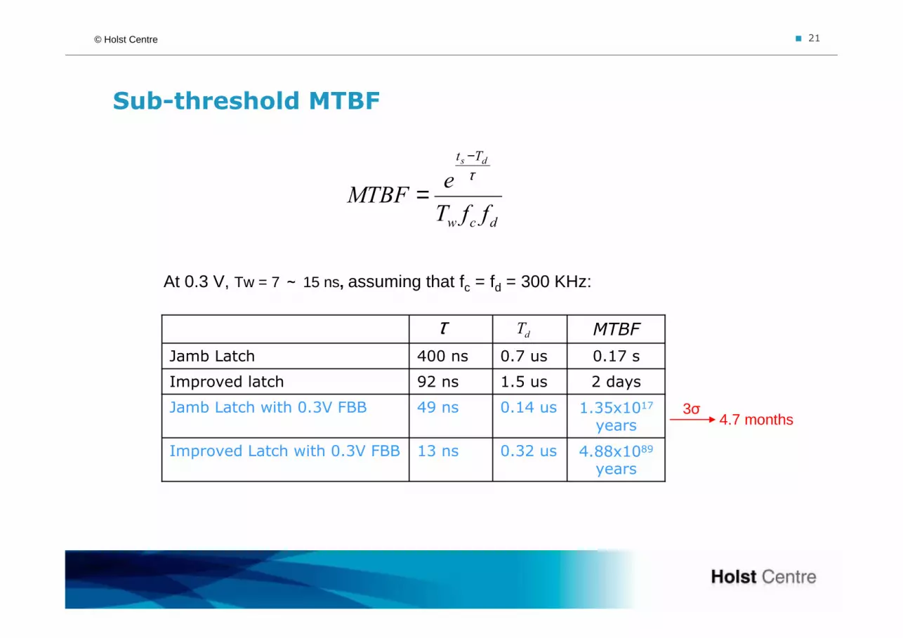
Sub-threshold MTBF
dcw
Tt
ffT
eMTBF
ds
τ−
=
1.35x10¹⁷
years0.14 us49 nsJamb Latch with 0.3V FBB
2 days1.5 us92 nsImproved latch
4.88x1089
years0.32 us13 nsImproved Latch with 0.3V FBB
0.17 s0.7 us400 nsJamb Latch
MTBFτ
At 0.3 V, Tw = 7 ~ 15 ns, assuming that fc = fd = 300 KHz:
dT
4.7 months3σ
• Sub-threshold Operation
• Synchronization in Multi-Low-VDD Systems on Chip
• Low Voltage Synchronizer Design
• Sub-threshold Synchronizer Design
• Results
• Implementation
• Conclusion
� 23© Holst Centre
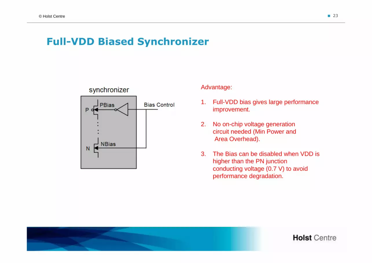
Full-VDD Biased Synchronizer
Advantage:
1. Full-VDD bias gives large performance improvement.
2. No on-chip voltage generation circuit needed (Min Power andArea Overhead).
3. The Bias can be disabled when VDD is higher than the PN junction conducting voltage (0.7 V) to avoid performance degradation.

• Sub-threshold Operation
• Synchronization in Multi-Low-VDD Systems on Chip
• Low Voltage Synchronizer Design
• Sub-threshold Synchronizer Design
• Results
• Implementation
• Conclusion
� 25© Holst Centre
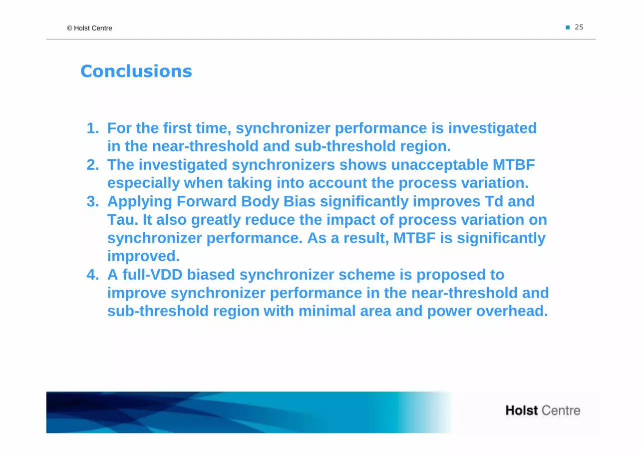
Conclusions
1. For the first time, synchronizer performance is investigated in the near-threshold and sub-threshold region.
2. The investigated synchronizers shows unacceptable MTBF especially when taking into account the process variation.
3. Applying Forward Body Bias significantly improves Td and Tau. It also greatly reduce the impact of process variation on synchronizer performance. As a result, MTBF is significantly improved.
4. A full-VDD biased synchronizer scheme is proposed to improve synchronizer performance in the near-threshold and sub-threshold region with minimal area and power overhead.

� 26© Holst Centre
Question?
Thank you !
Related Documents


![NetTM: Faster and Easier Synchronization for Soft ...steffan/talks/fpga11.pdf · Bloom filters [ARC10] Synch. Unit Conflict Detection Input mem. 18 Synch. Unit NetTM: extending NetThreads](https://static.cupdf.com/doc/110x72/5f346ad696d9a4257376de4c/nettm-faster-and-easier-synchronization-for-soft-steffantalksfpga11pdf.jpg)


