EXPERIMENT #7 PARALLEL INTERFACING USING THE PERIPHERAL INTERFACE ADAPTER (PIA) 1.0 Procedure The purpose of this experiment is to introduce the student to the following topics: • the Peripheral Interface Adapter IC (PIA, MC6821) • the MC68000’s Synchronous Bus Cycle • the MC68000’s Interrupt Generation Mechanism 2.0 Component Requirements Quantity: Description: (incl. Mfr., Mfr. Part No.) 1 Peripheral Interface Adapter (PIA); Motorola; MC6821 TBD Misc. TTL Logic Gates (AND, OR, inverters, buffers, decoders, etc.) 3.0 Background A. The Peripheral Interface Adapter (PIA) The Peripheral Interface Adapter or PIA, provides a general purpose means of interfacing peripheral equipment to the MC68000 and MC6800 family of microprocessors. This integrated circuit is capable of interfacing a microprocessor to peripheral devices through two 8-bit bi-directional peripheral data buses (PA0 to PA7, and PB0 to PB7) and four control lines (CA1, CA2, CB1, and CB2). The functional configuration of the PIA is programmable by the CPU during system initialization. Each of the sixteen peripheral data lines can be programmed to perform either as an input or an output line. Each of the peripheral control lines may be programmed to operate in one of several modes. The speed and ease of programmability provides a high degree of flexibility for the interface. Internal Architecture The PIA occupies four consecutive locations in the CPU’s memory map. The PIA contains six internal registers, three for Port A, and three for Port B. The two Register Select lines (RS1, RS0), are used to select one of the four registers inside the PIA. Saniie & Perich Experiment 7 - 1

Welcome message from author
This document is posted to help you gain knowledge. Please leave a comment to let me know what you think about it! Share it to your friends and learn new things together.
Transcript

EXPERIMENT #7
PARALLEL INTERFACING USING THE PERIPHERAL INTERFACE ADAPTER (PIA)
1.0 Procedure The purpose of this experiment is to introduce the student to the following topics:
• the Peripheral Interface Adapter IC (PIA, MC6821) • the MC68000’s Synchronous Bus Cycle • the MC68000’s Interrupt Generation Mechanism
2.0 Component Requirements Quantity: Description: (incl. Mfr., Mfr. Part No.)
1 Peripheral Interface Adapter (PIA); Motorola; MC6821 TBD Misc. TTL Logic Gates (AND, OR, inverters, buffers, decoders, etc.)
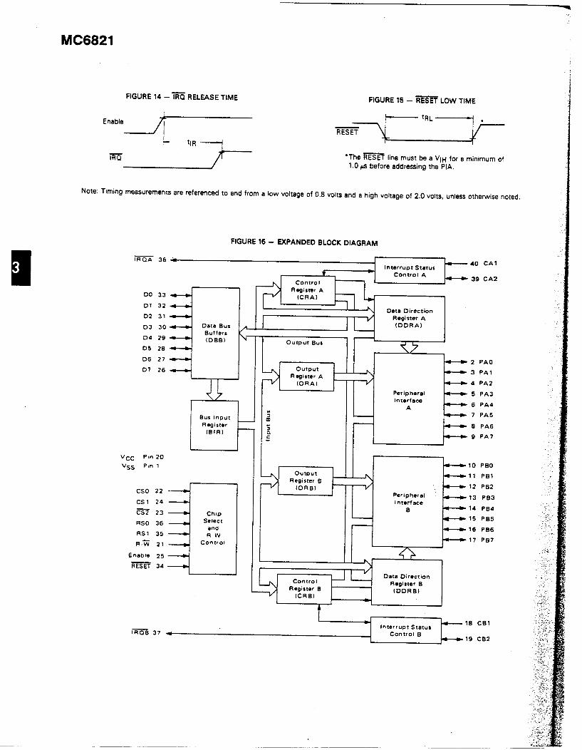
3.0 Background A. The Peripheral Interface Adapter (PIA) The Peripheral Interface Adapter or PIA, provides a general purpose means of interfacing peripheral equipment to the MC68000 and MC6800 family of microprocessors. This integrated circuit is capable of interfacing a microprocessor to peripheral devices through two 8-bit bi-directional peripheral data buses (PA0 to PA7, and PB0 to PB7) and four control lines (CA1, CA2, CB1, and CB2). The functional configuration of the PIA is programmable by the CPU during system initialization. Each of the sixteen peripheral data lines can be programmed to perform either as an input or an output line. Each of the peripheral control lines may be programmed to operate in one of several modes. The speed and ease of programmability provides a high degree of flexibility for the interface. Internal Architecture The PIA occupies four consecutive locations in the CPU’s memory map. The PIA contains six internal registers, three for Port A, and three for Port B. The two Register Select lines (RS1, RS0), are used to select one of the four registers inside the PIA.
Saniie & Perich Experiment 7 - 1

CR2 CRB2 RS1 RS0 PIA Register Selected 0 X 0 0 Data Direction Register, Port A 1 X 0 0 Peripheral Data Register, Port A X X 0 1 Control Register, Port A X 0 1 0 Data Direction Register, Port B X 1 1 0 Peripheral Data Register, Port B X X 1 1 Control Register, Port B These registers are defined as follows: 1. Data Direction Register (DDRA or DDRB)
This register programs each of the eight peripheral data lines (PA0 to PA7 or PB0 to PB7) to act as either an input or an output. Setting a bit equal to “1” defines its corresponding peripheral data line to be an output, while setting a bit equal to “0” defines its corresponding peripheral data line to be an input.
2. Peripheral Data Register (PDRA or PDRB)
Inputs
The signals from the peripheral data lines are input into this register. The CPU may then read this register to determine the status of the peripheral data lines. Outputs
The data written to this register by the CPU will appear on the peripheral data lines that are programmed as outputs. A “1” written into this register by the CPU causes a “high” level signal to appear on the corresponding peripheral data line. Similarly, a “0” written into this register by the CPU causes a “low” level signal to appear on the corresponding peripheral data line.
3. Control Register (CRA or CRB)
This register allows the CPU to configure the operation of the two peripheral control lines, CA1 and CA2 or CB1 and CB2. This register also allows the CPU to enable the interrupt lines and monitor the status of the interrupt flags. Bit 2 of this register is used, along with the Register Select lines (RS1, RS0), to determine whether the Data Direction Register or the Peripheral Data Register is to be accessed. A summary of the format of the control word is shown in the enclosed figures. The preceding discussion is meant to serve as a brief introduction to the PIA. For more detailed information about this device refer to the following texts:
Saniie & Perich Experiment 7 - 2

a. 8-Bit Microprocessor & Peripheral Data Book.
Series C. Austin, Texas: Motorola, Inc., 1983
b. Bishop, Ron. Basic Microprocessors and the 6800. Rochelle Park, NJ: Hayden Book Company, 1979. (refer specifically to Chapter 9)
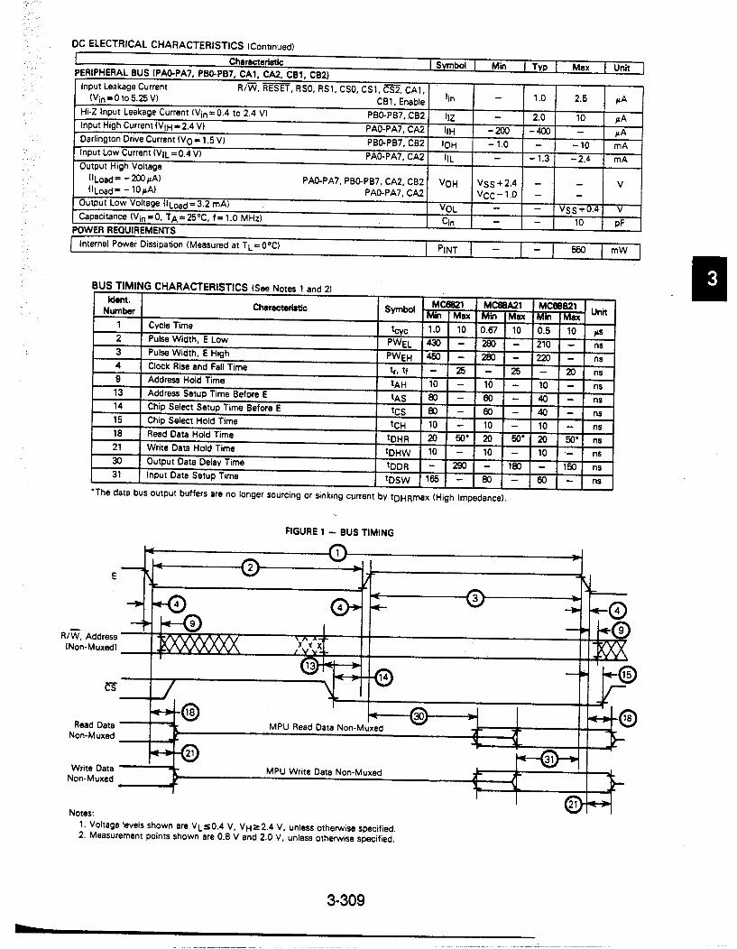
B. MC6800 Synchronous Bus Cycle In order for the 68000 to interface to 6800 type peripherals, the 68000 modifies its bus cycle to meet the 6800 bus cycle timing requirements whenever a 6800 type device is selected. This feature is possible because both types of processors use memory-mapped I/O. The 6800 interface is provided by three signals on the 68000. These signals are known as: Enable (E), Valid Peripheral Address (*VPA), and Valid Memory Address (*VMA). *VPA and *VMA are active-low signals. A description of each signal follows. 1. Enable (E)
Enable corresponds to the E or p2 (phase 2) signal in existing 6800 systems. It is the bus clock used by 6800 peripherals to synchronize data transfers. Enable is a free-running clock that is one-tenth the frequency of the 68000’s clock signal (CLK). It has a 60/40 duty cycle, which means that it is low for six of 68000 CLK cycles, and high for four of the 68000 CLK cycles. This extended duty cycle allows the 68000 to perform consecutive 6800 accesses.
2. Valid Peripheral Address (*VPA) This input signal informs the 68000 that the address on the bus is the address of a 6800 type device and that the bus should conform to the E clock transfer characteristics of the 6800 bus. VPA is derived by decoding the address bus, and qualifying it with Address Strobe (*AS).
3. Valid Memory Address (*VMA)
This output signal notifies any 6800 peripheral that the address on the address bus is valid, and that the 68000 is synchronized to the Enable (E) signal. The *VMA signal is used as part of the chip select circuitry for the peripheral. This ensures that 6800 type peripherals are selected and unselected at the proper time. The peripheral now runs its cycle during the high portion of the E signal. For more information about the 68000’s Synchronous Bus Cycle, refer to the chapter entitled “Signal and Bus Operation Description” in Motorola’s MC68000 8-/16-/32-Bit Microprocessors User’s Manual.
C. Interrupts
Saniie & Perich Experiment 7 - 3
Refer to the Background Section of Experiment #6. 4.0 Statement of Problem In this experiment the student will design and implement the hardware to interface the PIA to the SANPER-1 Educational Lab Unit. The student will also write software routines to write data to one port of the PIA and read it back on another port. 5.0 Preliminary Assignment 1. Draw a detailed schematic diagram of the hardware required to interface the PIA to
the SANPER-1 Educational Lab Unit.
The PIA must reside within the 64K address range of $050000 to $05FFFF. However, not all of this range is available. The following addresses are reserved for other hypothetical devices in the system. Device 1: $050000 - $050FFF Device 2: $053000 - $05407F Device 3: $055000 - $05603F Device 4: $059000 - $05A3FF Device 5: $05B000 - $05C0BF Device 6: $05E000 - $05FF00 The PIA may be placed in any non-occupied address locations within the 64K range. The user must decode around the above existing devices so that no other device is unintentionally selected. The user must initially use full address decoding to enter within the 64K address space at $50000. The user may then employ partial decoding and use a minimal number of address lines to select the PIA. HINT: Use one of the SANPER-1 ELU’s Block Select lines as part of your
address decoding implementation. The PIA’s Host or CPU interface must include all the signals shown on the left side of the PIA in Figure 7.1. Each of these signals should be connected to either the MC68000 or the address decoding logic. All unused inputs should be tied to +5V DC through a resistor. Connect the PIA *IRQ line(s) to the Interrupt Request Level 1 (*IRQ1) signal on the System Expansion Board of the SANPER-1 Educational Lab Unit. The PIA’s peripheral interface lines should be connected as shown on the right side of the PIA in Figure 7.1.
2. Build the hardware from Prelim #1 on breadboard strips.
Saniie & Perich Experiment 7 - 4

3. Write an initialization routine to configure the PIA for the following conditions:
• Port A lines (PA0 to PA7) are inputs • Port B lines (PB0 to PB7) are outputs • IRQA interrupt enabled and asserted by a high-to-low transition on CA1 • Port B uses pulse-mode handshaking
4. Write an Interrupt Service Routine (ISR) to read the peripheral data on PA0 to PA7
of Port A of the PIA whenever there is a high-to-low transition on CA1. Display the received character on the terminal.
Caution: Your ISR should not modify any registers unless they are first saved to the
stack. Restore the registers prior to exiting the ISR. 5. Write a program to continuously read a character from the keyboard and output it to
the peripheral data side of Port B of the PIA. 6. Write the main program, which executes the initialization subroutine of Prelim #2,
and then continuously executes the program of Prelim #5. 6.0 Procedure 1. Connect your hardware to the Breadboard Strip on the front panel of the SANPER-1
Educational Lab Unit. 2. Initialize the exception vector for the PIA interrupt request to point to the beginning
of the Interrupt Service Routine from Prelim #4. 3. Run the program from Prelim #6. 4. Press a key on the keyboard and record what happens at the terminal. You must be
able to explain the data that appears on the terminal. If no data is being displayed on the terminal, you have a problem, and you must
debug your hardware and software. If data is being displayed on the terminal, but you do not understand what is
happening, carefully review the functions of each of the preliminary assignments.
5. Demonstrate to your Lab Instructor that your hardware and software are working properly.
7.0 Discussion Submit the following to your Lab Instructor as a Final Report:
Saniie & Perich Experiment 7 - 5

Saniie & Perich Experiment 7 - 6
1. A fully commented listing of all programs and subroutines (they must include both global and local comments).
2. A schematic diagram of your hardware design. 3. Describe, in detail, the function of each of the programs from the Preliminary
Assignment. 4. Describe what type of interrupt acknowledge method (user or auto vectored) was
used for the PIA in this experiment and why? 5. Describe how a microprocessor determines which side of the PIA generated an
interrupt request? 6. If PIA Control Register A reads $3F, how has the PIA been configured? 7. Discuss three possible applications of the PIA. 8. Draw and discuss the timing diagram for a read operation using a MC68000
Synchronous Bus Cycle. Indicate the order in which the signals are asserted (and negated) and the timing relationships between them.


Related Documents