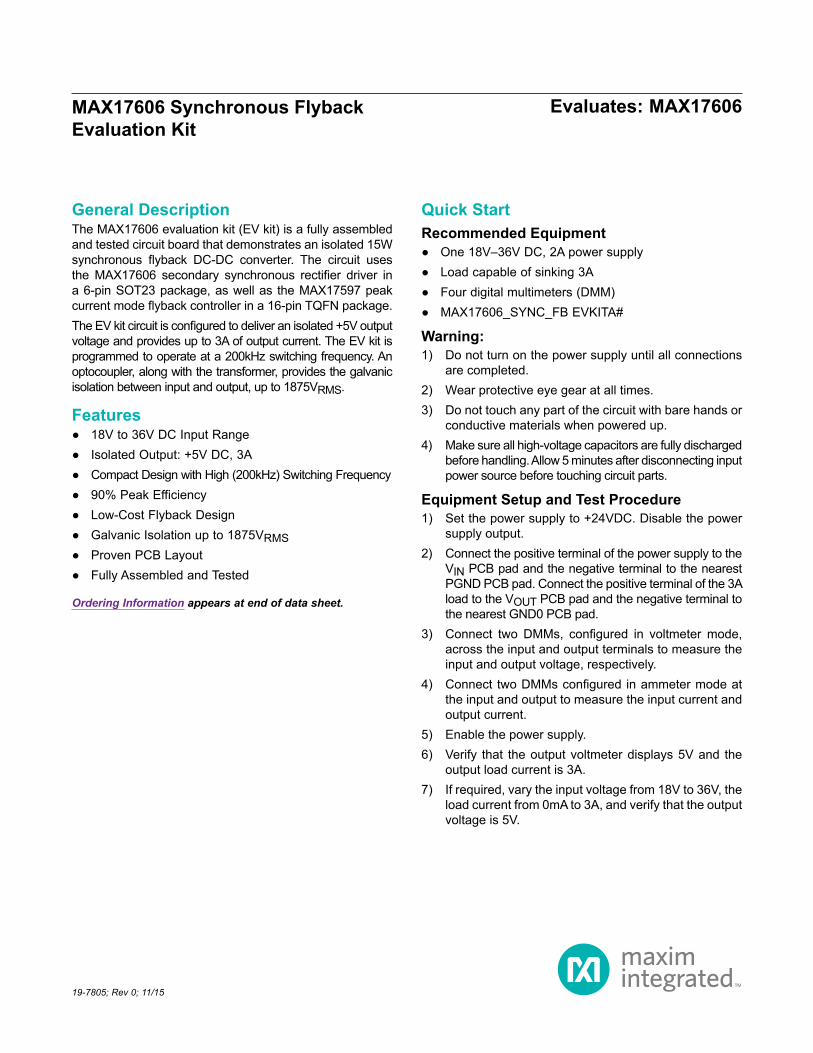
Evaluates: MAX17606 MAX17606 Synchronous Flyback Evaluation Kit General Description The MAX17606 evaluation kit (EV kit) is a fully assembled and tested circuit board that demonstrates an isolated 15W synchronous flyback DC-DC converter. The circuit uses the MAX17606 secondary synchronous rectifier driver in a 6-pin SOT23 package, as well as the MAX17597 peak current mode flyback controller in a 16-pin TQFN package. The EV kit circuit is configured to deliver an isolated +5V output voltage and provides up to 3A of output current. The EV kit is programmed to operate at a 200kHz switching frequency. An optocoupler, along with the transformer, provides the galvanic isolation between input and output, up to 1875V RMS . Features ● 18V to 36V DC Input Range ● Isolated Output: +5V DC, 3A ● Compact Design with High (200kHz) Switching Frequency ● 90% Peak Efficiency ● Low-Cost Flyback Design ● Galvanic Isolation up to 1875V RMS ● Proven PCB Layout ● Fully Assembled and Tested 19-7805; Rev 0; 11/15 Ordering Information appears at end of data sheet. Quick Start Recommended Equipment ● One 18V–36V DC, 2A power supply ● Load capable of sinking 3A ● Four digital multimeters (DMM) ● MAX17606_SYNC_FB EVKITA# Warning: 1) Do not turn on the power supply until all connections are completed. 2) Wear protective eye gear at all times. 3) Do not touch any part of the circuit with bare hands or conductive materials when powered up. 4) Make sure all high-voltage capacitors are fully discharged before handling. Allow 5 minutes after disconnecting input power source before touching circuit parts. Equipment Setup and Test Procedure 1) Set the power supply to +24VDC. Disable the power supply output. 2) Connect the positive terminal of the power supply to the V IN PCB pad and the negative terminal to the nearest PGND PCB pad. Connect the positive terminal of the 3A load to the V OUT PCB pad and the negative terminal to the nearest GND0 PCB pad. 3) Connect two DMMs, configured in voltmeter mode, across the input and output terminals to measure the input and output voltage, respectively. 4) Connect two DMMs configured in ammeter mode at the input and output to measure the input current and output current. 5) Enable the power supply. 6) Verify that the output voltmeter displays 5V and the output load current is 3A. 7) If required, vary the input voltage from 18V to 36V, the load current from 0mA to 3A, and verify that the output voltage is 5V.

Welcome message from author
This document is posted to help you gain knowledge. Please leave a comment to let me know what you think about it! Share it to your friends and learn new things together.
Transcript
Evaluates: MAX17606MAX17606 Synchronous Flyback Evaluation Kit
General DescriptionThe MAX17606 evaluation kit (EV kit) is a fully assembled and tested circuit board that demonstrates an isolated 15W synchronous flyback DC-DC converter. The circuit uses the MAX17606 secondary synchronous rectifier driver in a 6-pin SOT23 package, as well as the MAX17597 peak current mode flyback controller in a 16-pin TQFN package. The EV kit circuit is configured to deliver an isolated +5V output voltage and provides up to 3A of output current. The EV kit is programmed to operate at a 200kHz switching frequency. An optocoupler, along with the transformer, provides the galvanic isolation between input and output, up to 1875VRMS.
Features 18V to 36V DC Input Range Isolated Output: +5V DC, 3A Compact Design with High (200kHz) Switching Frequency 90% Peak Efficiency Low-Cost Flyback Design Galvanic Isolation up to 1875VRMS Proven PCB Layout Fully Assembled and Tested
19-7805; Rev 0; 11/15
Ordering Information appears at end of data sheet.
Quick StartRecommended Equipment
One 18V–36V DC, 2A power supply Load capable of sinking 3A Four digital multimeters (DMM) MAX17606_SYNC_FB EVKITA#
Warning: 1) Do not turn on the power supply until all connections
are completed. 2) Wear protective eye gear at all times. 3) Do not touch any part of the circuit with bare hands or
conductive materials when powered up. 4) Make sure all high-voltage capacitors are fully discharged
before handling. Allow 5 minutes after disconnecting input power source before touching circuit parts.
Equipment Setup and Test Procedure1) Set the power supply to +24VDC. Disable the power
supply output.2) Connect the positive terminal of the power supply to the
VIN PCB pad and the negative terminal to the nearest PGND PCB pad. Connect the positive terminal of the 3A load to the VOUT PCB pad and the negative terminal to the nearest GND0 PCB pad.
3) Connect two DMMs, configured in voltmeter mode, across the input and output terminals to measure the input and output voltage, respectively.
4) Connect two DMMs configured in ammeter mode at the input and output to measure the input current and output current.
5) Enable the power supply.6) Verify that the output voltmeter displays 5V and the
output load current is 3A.7) If required, vary the input voltage from 18V to 36V, the
load current from 0mA to 3A, and verify that the output voltage is 5V.

Maxim Integrated 2www.maximintegrated.com
Evaluates: MAX17606MAX17606 Synchronous Flyback Evaluation Kit
Detailed DescriptionThe MAX17606 EV kit provides a proven design to evaluate the MAX17606. The device is a secondary-side synchronous driver and controller specifically designed for the isolated flyback topology. By replacing the secondary diode with a MOSFET, the MAX17606 improves efficiency and makes thermal management easier. The device EV kit is configured for a 5V output voltage, supplying up to 3A of current.This EV kit uses the peak current mode, pulse-width modulating (PWM) controller IC MAX17597 in a 16-pin TQFN package with an exposed pad as the primary-side flyback controller. This PWM controller varies the duty cycle to compensate for the variation in input voltage (VIN) and the output load to maintain a constant output voltage.The detailed description of flyback design calculations are described in Application Note 5504, “Designing Flyback Converters Using Peak Current-Mode Controllers.” The details of soft-start time programming, programming output voltage, peak-current limit setting, switching frequency setting and the EN/UVLO, OVI settings are described in the MAX17595/6/7 data sheet.The MAX17606 has a wide range of input voltage from 4.5V to 36V. The input range makes it simple to drive using one of the following two methods. When the output voltage is 5V and greater, VOUT can be used to directly drive VIN. When the output voltage is less than 5V, use the rectified drain voltage of the secondary synchronous MOSFET to drive VIN. The EV kit circuit has an option for both of these configurations. By default, the EV kit is programmed to run from the rectified drain voltage of the synchronous MOSFET. When running the MAX17606 from the output voltage is required, remove R1 and set R31 to 10Ω.
The device has a provision to program the turn-off trip point of the secondary synchronous rectifier. An external resistor (R25) connects the drain of the external MOSFET to the IC’s DRN pin. This resistor sets the turn-off trip point with a precise internal current source. Once the synchronous rectifier is turned off, the MAX17606 uses resistor R26 (connected between the TOFF pin and GND0) to program the turn-off time in order to provide immunity from DCM ringing. For the selection of R25 and R26 resistors, refer to the MAX17606 data sheet.Note: The EV kit is shipped with frequency dithering disabled and the DITHER/SYNC pin shorted to SGND by a 0Ω resistor. To set the desired frequency dither, replace R23 with a capacitor of appropriate value, as detailed in the MAX17595/6/7 data sheet. The DITHER /SYNC PCB pad is available for monitoring the signal at the DITHER/SYNC pin.
Maxim Integrated 3www.maximintegrated.com
Evaluates: MAX17606MAX17606 Synchronous Flyback Evaluation Kit
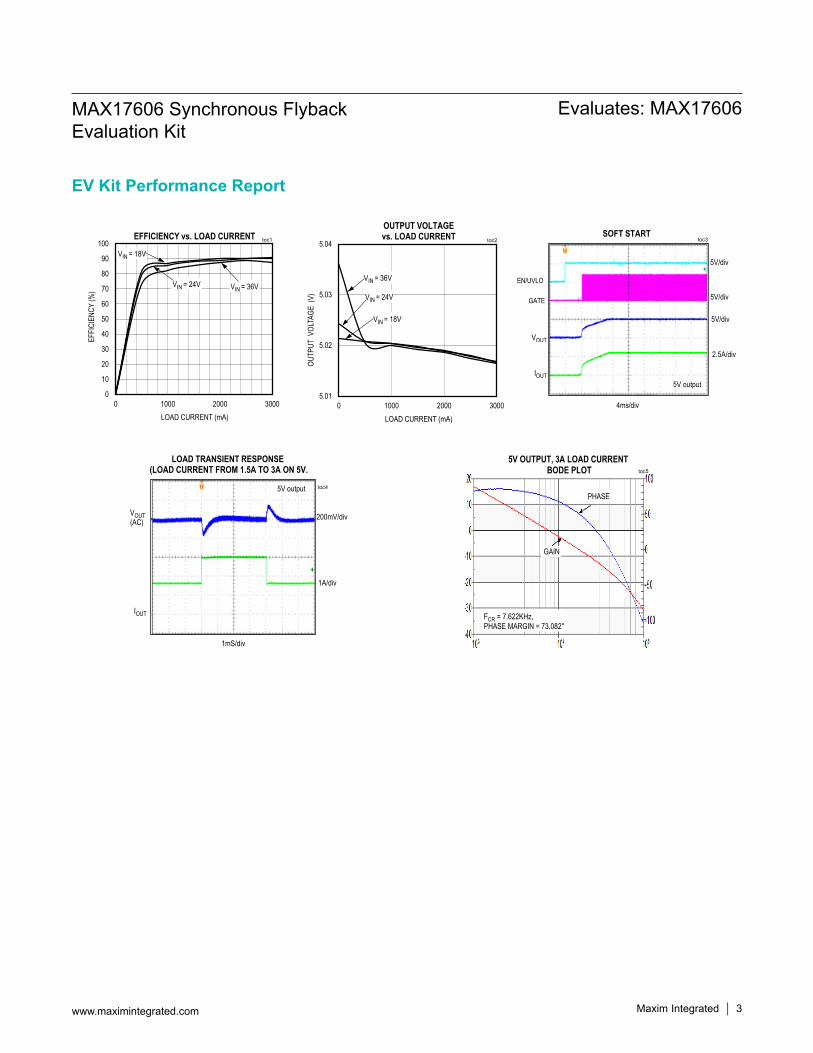
EV Kit Performance Report
0
10
20
30
40
50
60
70
80
90
100
0 1000 2000 3000
EFFI
CIEN
CY(%
)
LOAD CURRENT (mA)
EFFICIENCY vs. LOAD CURRENT toc1
VIN = 36VVIN = 24V
VIN = 18V
200mV/div
1A/div
toc4
1mS/div
VOUT(AC)
IOUT
LOAD TRANSIENT RESPONSE (LOAD CURRENT FROM 1.5A TO 3A ON 5V.
5V output
toc5
5V OUTPUT, 3A LOAD CURRENTBODE PLOT
F
PHASE
GAIN
CR = 7.622KHz,PHASE MARGIN = 73.082°
5V/div
2.5A/div
toc3
4ms/div
VOUT
IOUT
SOFT START
EN/UVLO
GATE
5V/div
5V/div
5V output5.01
5.02
5.03
5.04
0 1000 2000 3000
OUTP
UT V
OLTA
GE (
V)
LOAD CURRENT (mA)
OUTPUT VOLTAGEvs. LOAD CURRENT toc2
VIN = 36V
VIN = 24V
VIN = 18V
Maxim Integrated 4www.maximintegrated.com
Evaluates: MAX17606MAX17606 Synchronous Flyback Evaluation Kit
#Denotes RoHS compliant.
Note: Indicate that you are using the MAX17606SFBEVKIT when contacting these component suppliers.
Component Suppliers
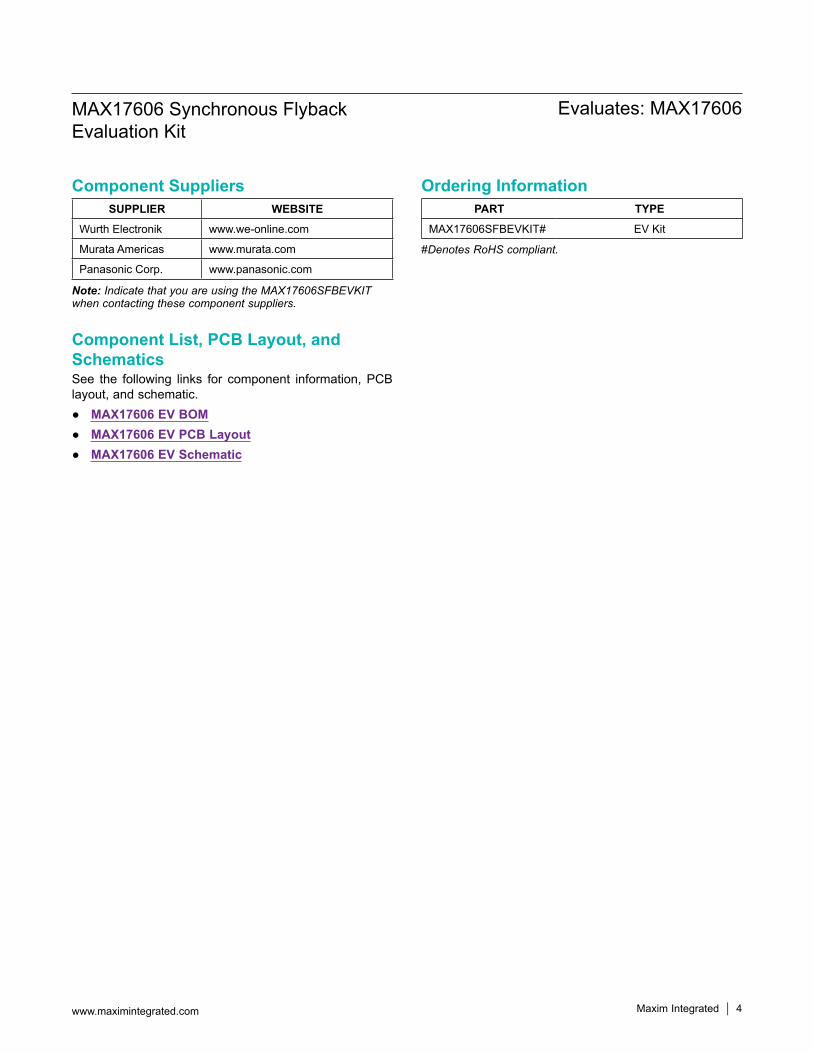
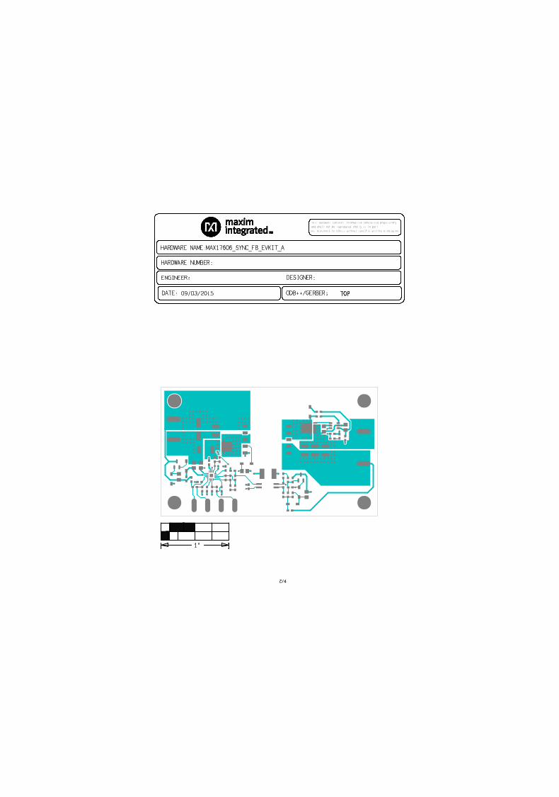
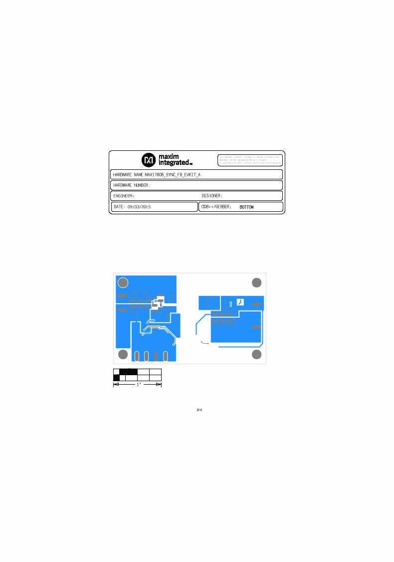
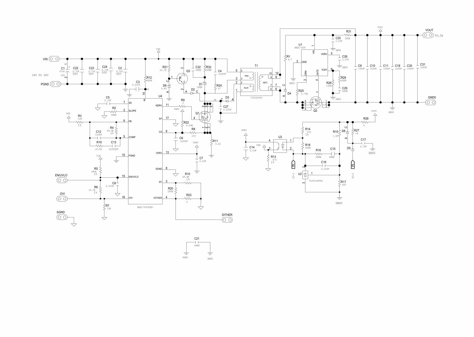
Component List, PCB Layout, and SchematicsSee the following links for component information, PCB layout, and schematic.
MAX17606 EV BOM MAX17606 EV PCB Layout MAX17606 EV Schematic
Ordering InformationSUPPLIER WEBSITE
Wurth Electronik www.we-online.com
Murata Americas www.murata.com
Panasonic Corp. www.panasonic.com
PART TYPE
MAX17606SFBEVKIT# EV Kit

Maxim Integrated cannot assume responsibility for use of any circuitry other than circuitry entirely embodied in a Maxim Integrated product. No circuit patent licenses are implied. Maxim Integrated reserves the right to change the circuitry and specifications without notice at any time.
Maxim Integrated and the Maxim Integrated logo are trademarks of Maxim Integrated Products, Inc. © 2015 Maxim Integrated Products, Inc. 5
Evaluates: MAX17606MAX17606 Synchronous Flyback Evaluation Kit
Revision HistoryREVISIONNUMBER
REVISIONDATE DESCRIPTION PAGES
CHANGED
0 11/15 Initial release —
For pricing, delivery, and ordering information, please contact Maxim Direct at 1-888-629-4642, or visit Maxim Integrated’s website at www.maximintegrated.com.

GND0
VOUT
SILK_TOP
R31
C25
C29
R25R1
U1
C26
R26
C9
R29
C17
REV-A
09/15 MS
and shall not be reproduced wholly or in part,
This document contains information considered proprietary,
nor disclosed to others without specific written permission.
D4
Q2
C11C18
U2
R27
D5
DESIGNER:
ODB++/GERBER:
C16
C15
R17
C21R18R16
R15
R14
D8
R28
1/4
D3
C27
U3
T1
R4
C12R3
C14
C13
R19
C2
Q1
R22
C5
R13C6
U4
R20 R23
DITHER
SGND
1-888-629-4642 www.maximintegrated.com
MAX17606_SYNC_FB EVKIT
R9R8
R5 C7
C8
R7R2
R10
OVI
1"
09/03/2015
C1
R11
D2 C3
R6
R12
R21
EN/UVLO
HARDWARE NUMBER:
HARDWARE NAME:MAX17606_SYNC_FB_EVKIT_A
ENGINEER:
DATE:
VIN
PGND
Q3
D6
TOP
and shall not be reproduced wholly or in part,
This document contains information considered proprietary,
nor disclosed to others without specific written permission.
DESIGNER:
ODB++/GERBER:
2/4
1"
09/03/2015
HARDWARE NUMBER:
HARDWARE NAME:MAX17606_SYNC_FB_EVKIT_A
ENGINEER:
DATE:
BOTTOM
and shall not be reproduced wholly or in part,
This document contains information considered proprietary,
nor disclosed to others without specific written permission.
DESIGNER:
ODB++/GERBER:
3/4
1"
09/03/2015
HARDWARE NUMBER:
HARDWARE NAME:MAX17606_SYNC_FB_EVKIT_A
ENGINEER:
DATE:
SILK_BOT
C31
and shall not be reproduced wholly or in part,
This document contains information considered proprietary,
nor disclosed to others without specific written permission.
C10
C30
DESIGNER:
ODB++/GERBER:
4/4
C32
C4
R32
R24 D1
C24
C23
1"
09/03/2015
C22
HARDWARE NUMBER:
HARDWARE NAME:MAX17606_SYNC_FB_EVKIT_A
ENGINEER:
DATE:

S NO Designation Qty Description Manufacturer Partnumber‐1 Manufacturer Partnumber‐2 Manufacturer Partnumber‐3
1 C1 147µF±20%, 50V,ALUMINUM‐ELECTROLYTIC
SMT(CASE_D8) PANASONIC EEEFK1H470XP
2 C2, C22‐C24 4 4.7µF±10% 50V X7R Ceramic capacitor (1210) Murata GRM32ER71H475KA88K KEMET C1210C475K5RAC
3 C3, C27 2 0.22µF±10%,50V, X7R ceramic capacitor (0805) Murata GRM21BR71H224KA KEMET C0805C224K5RAC TDK CGJ4J2X7R1H224K125AA
4 C4 1 1000pF±10%,100V,X7R ceramic capacitor (0402) Murata GRM155R72A102KA01
5 C5,C14 2 0.1µF±10%, 25V, X7R ceramic capacitor(0603) TDK C1608X7R1E104K080AA
6 C6 1 1000pF±5%,50V, X7R ceramic capacitor (0402) Murata GRM155R71H102JA01D
7 C7, C25, C26 3 2.2µF ±10%,50V, X7R ceramic capacitor (0805) TDK C2012X7R1H225K
8 C8 1 0.01µF±5%, 50V, X7R ceramic capacitor(0603) KEMET C0603X7R500103JNP KEMET C0603C103J5
9 C9‐C11, C18, C30, C31 6 100µF±20%, 6.3V, X5R ceramic capacitor (1210) Murata GRM32ER60J107ME20 KEMET C1210C107M9PAC VENKEL LTD C1210X5R6R3‐107MNE
10 C12 1 120pF, 1%, 50V, COG ceramic capacitor (0603) KEMET C0603C121K5GAC
11 C13 1 22000pF, 10%, 25V, X7R ceramic capacitor (0603) KEMET C0603C223K3RAC
12 C15,C29,C32 3 OPEN (0603)
13 C16 1 0.22uF±10%, 25V, X7R ceramic capacitor(0603) KEMET C0603C224K3RACMurata
GRM188R71E224KA8 KEMET C1608X7R1E224K08
14 C17 1 4.7µF ±10%,16V, X7R ceramic capacitor (0805) Murata GRM21BR71C475KA73
15 C21 1 OPEN (1812)
16 D1 1 OPEN (SOD‐123FL)
17 D2‐D5,D8 5 100V/0.3A, (SOD123), DIODE DIODES INCORPORATED 1N4148W‐7‐F
18 D6 1 6.8V/3UA, (SOD123), DIODE, ZENER ON SEMICONDUCTOR MMSZ5235BT1G
19 Q1 1100V/22A/69W, POWER‐56(8‐PQFN),POWER‐
TRANSISTORFAIRCHILD SEMICONDUCTOR
FDMS86102LZ
20 Q2 1 40V/73A/5W, TSDSON‐8 PACKAGE ,POWER‐TRANSISTOR INFINEON BSZ040N04LSG
21 Q3 1 60V/0.5A/0.35W, SOT‐23 ,HIGH VOLTAGE AMPLIFIERFAIRCHILD SEMICONDUCTOR
MMBTA05
22 R1 1 4.7Ω ±5% resistor (0603) VISHAY DALE CRCW06034R70JN
23 R2,R12,R16,R18, R20,R29,R31 7 OPEN (0603)
24 R3 1 22kΩ ±1% resistor (0603) VISHAY DALE CRCW060322K0FK
25 R4, R10 2 49.9kΩ ±1% resistor (0603) VISHAY DALE CRCW060349K9FK PANASONIC ERJ‐3EKF4992V

26 R5 1 280kΩ ±1% resistor (0603) VISHAY CRCW0603280KFK
27 R6 1 10.7kΩ ±5% resistor (0603) VISHAY CRCW060310K7FK PANASONIC ERJ‐3EKF1072V
28 R7 1 10kΩ ±1% resistor (0603) VISHAY DALE CHPHT0603K1002FGT
29 R8 1 220Ω ±1% resistor (0603) VISHAY DALE CRCW0603220RFK
30 R9, R23, R28 3 0Ω ±0% resistor (0603) VISHAY DALE CRCW06030000ZS ROHM MCR03EZPJ000 PANASONIC ERJ‐3GEY0R00
31 R11 1 0.02Ω ±1% resistor (2010) TT ELECTRONICS LRC‐LRF2010LF‐01‐
R020F
32 R13, R14 2 470Ω ±1% resistor (0603) VISHAY DALE CRCW0603470RFK PANASONIC ERJ‐3EKF4700
33 R15 1 1.5kΩ ±1% resistor (0603) VISHAY DALE CRCW06031K50FK
34 R17 1 487Ω ±1% resistor (0603) PANASONIC ERA‐3AEB4870
35 R19 1 10.5kΩ ±1% resistor (0603) VENKEL LTD CR0603‐16W‐1052FT
36 R21 1 22.1kΩ ±1% resistor (0805) VISHAY DALE CRCW080522K1FK
37 R22 1 4.99kΩ ±1% resistor (0603) VISHAY DALE CRCW06034K99FKPANASONIC ERJ‐ERJ‐
3EKF4991V
38 R24 1 47Ω ±1% resistor (1210) VISHAY DRALORIC
CRCW121047R0JNEAHP
39 R25 1 2.74kΩ ±1% resistor (0603) VISHAY DALE CRCW06032K74FK
40 R26 1 100kΩ ±1% resistor (0603) VISHAY DALE CRCW06031003FK PANASONIC ERJ‐3EKF1003
41 R27 1 1kΩ ±1% resistor (0603) VISHAY DALE CRCW06031001FK PANASONIC ERJ‐3EKF1001V
42 R32 1 OPEN (1210)
43 T1 1 EP13,10‐pin SMT, 9µH,5A, (3‐5):(10‐6):(2‐1) = 1:0.33:0.55 WURTH ELECTRONICS INC. 750342955
44 U1 1 MAX17606, 6L THIN SOT23, Flyback converters MAX17606AZT+
45 U2 1 Shunt regulator ,SOT23 DIODES INCORPORATED TLV431BFTA
46 U3 1 PHOTOTRANSISTOR OPTOCOUPLERAVAGO TECHNOLOGIES ACPL‐217‐
56AE
47 U4 1MAX17597 TQFN16‐EP,PEAK‐CURRENT‐MODE
CONTROLLERFOR FLYBACK MAX17597ATE+
18V TO 36V
PGND
GND0
5V,3A
GND0
GND0
OPEN
100UF 100UF 100UFC31
VOUT
C9100UF
C10 C11100UF
C18100UF
C30
GND0
C25
MAX17606
4.7
OPEN
0
22000PF
0.01UF
1%
OPEN6.8V
IN
22.1K
VDRV
OPEN
0.22UF
OPEN
GND0
0
OPEN OPEN
OPEN
VOUT
OPEN
2.2UF
1000PF
OPEN
OPEN
0.22UF
OPEN
OPEN
1%280K
MAX17597ATE+
120PF
4.7UF
50V
GND0
GND0
GND0
VIN
U3-2
VDRVVFB
IN
VFB
U3-2
VDRV
750342955
0.02
220
22K
0.1UF
0.1UF
2.74K
0.22UF
TLV431BFTA
2.2UF
1000PF
10K
4.7UF
1K
10.7K
10.5K
487
470
4.99K
100K
49.9K
0
49.9K
47
4.7UF4.7UF4.7UF47UF
470
1.5K
2.2UF
1%
1%
1%
1%
1%
50V50V50V50V
VIN
SGND
OVI
EN/UVLO
R6
R5
R3
PGND
VIN
R20
R10
R4
R2
C2
C3
C6
R9
D1
DITHER
C14
R13
U314
3 2R18
R16
GND0
VOUT
C15 D5
U4
5
9
4
15
176
11
16
10
8
2
7
13
14
C21
R12
R24
C4
D6
AC
R21Q3
1
32 D2
A C
D3AC
C27
C12
R19 C13
R8
R22
U2
32
1
C16
R14R15
R17
C17
R1
U1
3 4
2
6
5
1
D4
AC
R25
R26
R27
R31
C7
C26
R11
C8
C5
R29
C29
R7
R28
T1
1
23
5
67
910
C11
2C24C23C22
D8
AC
Q1
5 6 7 8
4
1 2 3
R32C32
Q2
5678
4
123
R23
3
TOFF
VDRV
GAT
E
DRN
GND
VIN
B
E
C
DITHER
EP
OVI
EN/UVLO
IN
VDRV
NDRV
PGND
CS
SGND
SS
FB
COMP
RT
SLOPE
ININ
SD G
S
D
G
+
SEC
AUX
PRI10
93
76
5
2
1
Related Documents