EVAL80960VH Evaluation Platform Board Manual December 1998 Order Number: 273194-003

Welcome message from author
This document is posted to help you gain knowledge. Please leave a comment to let me know what you think about it! Share it to your friends and learn new things together.
Transcript

EVAL80960VH Evaluation PlatformBoard Manual
December 1998
Order Number: 273194-003

EVAL80960VH Evaluation Platform Board Manual
Information in this document is provided in connection with Intel products. No license, express or implied, by estoppel or otherwise, to any intellectual property rights is granted by this document. Except as provided in Intel’s Terms and Conditions of Sale for such products, Intel assumes no liability whatsoever, and Intel disclaims any express or implied warranty, relating to sale and/or use of Intel products including liability or warranties relating to fitness for a particular purpose, merchantability, or infringement of any patent, copyright or other intellectual property right. Intel products are not intended for use in medical, life saving, or life sustaining applications.
Intel may make changes to specifications and product descriptions at any time, without notice.
Designers must not rely on the absence or characteristics of any features or instructions marked "reserved" or "undefined." Intel reserves these for future definition and shall have no responsibility whatsoever for conflicts or incompatibilities arising from future changes to them.
The EVAL80960VH Evaluation Platform may contain design defects or errors known as errata which may cause the product to deviate from published specifications. Current characterized errata are available on request.
Contact your local Intel sales office or your distributor to obtain the latest specifications and before placing your product order.
Copies of documents which have an ordering number and are referenced in this document, or other Intel literature may be obtained by calling 1-800-548-4725 or by visiting Intel’s website at http://www.intel.com.
Copyright © Intel Corporation, 1998
*Third-party brands and names are the property of their respective owners.

Contents1 Introduction
1.1 EVAL80960VH Features ....................................................................................1-21.2 CTOOLS Software Development Toolset ..........................................................1-2
1.2.1 CTOOLS and the MON960 Debug Monitor...........................................1-21.2.1.1 MON960 Host Communications...............................................1-31.2.1.2 Terminal Emulation Mode ........................................................1-31.2.1.3 Host Debugger Interface Library (HDI) Mode...........................1-3
1.3 About This Manual .............................................................................................1-31.4 Notational Conventions ......................................................................................1-41.5 Technical Support ..............................................................................................1-4
1.5.1 Intel Customer Electronic Mail Support .................................................1-51.5.2 Intel Customer Literature and Telephone Support ................................1-51.5.3 Related Information ...............................................................................1-5
2 Getting Started
2.1 Pre-installation Considerations...........................................................................2-12.1.1 Software Development Tools ................................................................2-1
2.2 Software Installation ...........................................................................................2-12.2.1 Installing Software Development Tools .................................................2-1
2.3 Hardware installation..........................................................................................2-22.3.1 Installing the EVAL80960VH Platforms in the Host System..................2-22.3.2 Verify EVAL80960VH Platform is Functional ........................................2-2
2.4 Creating and Downloading Executable Files......................................................2-22.4.1 Sample Download and Execution Using gdb960 ..................................2-2
3 Hardware Reference
3.1 Connectors, Switches and LEDs........................................................................3-13.2 Power Requirements..........................................................................................3-23.3 DRAM.................................................................................................................3-2
3.3.1 DRAM Performance ..............................................................................3-23.3.2 Upgrading DRAM ..................................................................................3-3
3.4 ROM and Flash ROM.........................................................................................3-33.5 Serial Port...........................................................................................................3-43.6 Logic Analyzer Headers .....................................................................................3-43.7 Expansion Connectors .......................................................................................3-63.8 JTAG Header .....................................................................................................3-83.9 Switch Settings...................................................................................................3-83.10 User LEDs ..........................................................................................................3-9
3.10.1 User LEDs During Initialization............................................................3-103.11 Serial EEPROM (I2C) .......................................................................................3-10
4 i960® VH Processor Overview
4.1 CPU Memory Map..............................................................................................4-14.1.1 Booting Out of DRAM on the EVAL80960VH Platform .........................4-3
4.2 Local Interrupts...................................................................................................4-34.3 CPU Counter/Timers ..........................................................................................4-5
EVAL80960VH Evaluation Platform Board Manual iii

4.4 PCI Interface ......................................................................................................4-54.5 DMA Channels ...................................................................................................4-5
5 MON960 Support for EVAL80960VH
5.1 MON960 Components .......................................................................................5-15.1.1 mon960 Initialization .............................................................................5-15.1.2 80960 JT Core Initialization...................................................................5-15.1.3 Memory Controller Initialization .............................................................5-25.1.4 PCI Interface Initialization .....................................................................5-2
5.1.4.1 Mode 0 .....................................................................................5-25.1.4.2 Mode 1 .....................................................................................5-35.1.4.3 Mode 2 .....................................................................................5-3
5.1.5 ATU Initialization ...................................................................................5-35.2 mon960 Kernel...................................................................................................5-45.3 Diagnostics.........................................................................................................5-4
5.3.1 Board Level Diagnostics .......................................................................5-4
A Bill of Materials ............................................................................................................... A-1
B Schematics..................................................................................................................... B-1
C PLD Code....................................................................................................................... C-1
D Backplane 0015 Interface .............................................................................................. D-1
D.1 Introduction ....................................................................................................... D-1D.2 Installing the EVAL80960VH into the Backplane 0015 ..................................... D-1D.3 Powering the EVAL80960VH/Backplane System ............................................. D-1D.4 Interrupt Routing and IDSELs on the Backplane 0015 ..................................... D-2D.5 PCI Host Detection and Configuration .............................................................. D-4D.6 PCI Initialization ................................................................................................ D-4D.7 PCI Bios Routines ............................................................................................. D-4D.8 Additional MON960 Commands........................................................................ D-9D.9 Bill of Material.................................................................................................... D-9D.10 Schematics...................................................................................................... D-11D.11 PAL Code ........................................................................................................ D-16
Figures
1-1 EVAL80960VH Platform Functional Block Diagram...........................................1-13-1 EVAL80960VH Platform Physical Diagram........................................................3-13-2 Expansion Connector Pin Numbering ................................................................3-63-3 LED Register Bitmap..........................................................................................3-94-1 i960® VH Processor Block Diagram ..................................................................4-14-2 EVAL80960VH Platform Memory Map...............................................................4-24-3 Interrupt Controller Connections ........................................................................4-44-4 i960® VH Processor DMA Controller .................................................................4-5D-1 EVAL80960VH Backplane Board Illustration .................................................... D-2D-2 EVAL80960VH/Backplane 0015 with Eval Board Installed ............................... D-3D-3 EVAL80960VH/Backplane 0015 Installation ..................................................... D-3
iv EVAL80960VH Evaluation Platform Board Manual

Tables
3-1 EVAL80960VH Connectors and LEDS ..............................................................3-13-2 EVAL80960VH Platform Power Requirements (Clock Mode DX4)....................3-23-3 DRAM Performance ...........................................................................................3-33-4 DRAM Configurations.........................................................................................3-33-5 ROM Select ........................................................................................................3-33-6 UART Register Addresses .................................................................................3-43-7 Logic Analyzer Header Definitions ....................................................................3-43-8 Expansion Connector Definitions .......................................................................3-63-9 JTAG Header Pinout, Connector J2..................................................................3-83-10 Switch S1 Settings .............................................................................................3-83-11 Startup LEDs MON960.....................................................................................3-104-1 DRAM Mapping ..................................................................................................4-34-2 DBAR Settings for Booting out of DRAM ...........................................................4-35-1 Initialization Modes.............................................................................................5-2A-1 EVAL80960VH Bill of Materials......................................................................... A-1D-1 PCI Interrupt Routing and IDSELs .................................................................... D-2D-2 Backplane 0015 Interface Bill of Material .......................................................... D-9
EVAL80960VH Evaluation Platform Board Manual v


d-
n, T core ler
Introduction 1
This manual describes the EVAL80960VH evaluation platform for Intel’s i960® VH embeddePCI processor. The i960 VH processor (“80960VH”) addresses the needs of I/O processor applications by enabling communications, through message passing and interrupt generatiobetween it and a host processor or external PCI device. The 80960VH combines an 80960Jwith a PCI bus interface, as well as a memory controller, DMA channels, an interrupt controlinterface, and an I2C Serial Bus. The EVAL80960VH evaluation platform is a half-length PCI adapter board. The board can be installed in any PCI host system that complies with the PCI Local Bus Specification, revision 2.1.
Figure 1-1. EVAL80960VH Platform Functional Block Diagram
Exp
ansi
on C
onne
ctor
Primary PCIInterface
i960® VHProcessor
FlashROM
I2C
LED UART
User LEDs
ConsolePort
SerialEEPROM
DRAM
RS-232
HostSystem
Local Bus
EVAL80960VH Evaluation Platform Board Manual 1-1

Introduction
ce, w and
for ovide bler, ent.
that
nning
1.1 EVAL80960VH Features
The i960® VH embedded-PCI processor serves as the main component of a high performanPCI-based I/O subsystem. The features of the EVAL80960VH platform are enumerated beloshown in Figure 1-1 and Figure 3-1.
• i960® VH embedded-PCI processor
• PCI short-card form factor
• 32-bit primary PCI bus interface
• 4 Mbytes DRAM expandable to 32Mbytes using 72-pin, 5V SIMM socket supporting EDO DRAM organized x32 or x36
• 2 DMA channels on PCI bus
• I2C Serial Bus
• IK byte serial EEPROM (24C08) (connected to I2C bus for developer application use)
• Serial console port based on 16C550 UART
• Eight user-programmable LEDs
• 2 Indicator LEDs: processor has failed self-test, and processor is running
• Socketed flash ROM and on-board flash ROM devices
• Logic analyzer connectors for ROM bus and processor interface signals
• Processor local bus expansion header
• SMT dip switch for setting processor configuration signal defaults
• JTAG header (supports JTAG debugger interface)
1.2 CTOOLS Software Development Toolset
Intel’s i960 processor software development toolset (CTOOLS) features advanced C/C++- language compilers for the i960 processor family. CTOOLS development toolset is availableWindows* 95/NT-based systems and a variety of UNIX workstation hosts. These products prexecution profiling and instruction scheduling optimizations. The tools also include an assemlinker, symbolic debugger, and utilities designed for embedded processor software developm
1.2.1 CTOOLS and the MON960 Debug Monitor
The EVAL80960VH platform is equipped with Intel’s mon960, an on-board software monitor allows you to execute and debug programs written for i960 processors. The monitor provides program download, breakpoint, single step, memory display, and other useful functions for ruand debugging a program.
The EVAL80960VH platform works with the source-level debuggers provided with CTOOLS,including gdb960 (command line version) and gdb960V (GUI version).
1-2 EVAL80960VH Evaluation Platform Board Manual

Introduction
al or r more
1.2.1.1 MON960 Host Communications
In a host system, mon960 allows you to communicate and download programs developed for the EVAL80960VH platform using the serial port, the PCI interface, or the JTAG interface. The EVAL80960VH platform supports two modes of serial connection: terminal emulation and Host Debugger Interface (HDI). The PCI and JTAG interfaces only support the HDI mode.
1.2.1.2 Terminal Emulation Mode
Terminal emulation software on your host system can communicate to mon960 on the EVAL80960VH platform via an RS-232 serial port. The EVAL80960VH platform supports port speeds from 300 to 115,200 bps. Downloading program code in this mode requires that the terminal emulation software support the XMODEM protocol.
Configure the serial port on the host system for 300-115,200 baud, 8 bits, one stop bit, no parity with XON/XOFF flow control. Six carriage returns must be sent to initiate this mode.
1.2.1.3 Host Debugger Interface Library (HDI) Mode
You may use a source-level debugger, such as Intel’s gdb960 and gdb960V to establish seriPCI, or JTAG communications with the EVAL80960VH platform. The mon960 Host DebuggeInterface (HDI) provides a defined messaging layer between mon960 and the debugger. Forinformation on this interface, see the MON960 Debug Monitor User’s Guide (Intel order number 484290).
HDI connection requests cannot be detected by mon960 if the user has already initiated a connection using a terminal emulator, or vice versa. Once one mode is initiated, the EVAL80960VH platform must be reset before a different mode can be selected.
1.3 About This Manual
A brief description of the contents of this manual follows.
Chapter 1, “Introduction”Introduces the EVAL80960VH evaluation board features. This chapter also describes Intel’s CTOOLS software development tools, and defines notational conventions and related documentation.
Chapter 2, “Getting Started”
Provides step-by-step instructions for installing the EVAL80960VH platform in a host system and downloading and executing an application program. This chapter also describes Intel’s software development tools, the MON960 Debug Monitor, software installation, and hardware configuration.
Chapter 3, “Hardware Reference”
Describes the locations of connectors, switches and LEDs on the EVAL80960VH. Header pinouts and register descriptions are also provided in this chapter.
Chapter 4, “i960® VH Processor Overview”
Presents an overview of the capabilities of the i960® VH embedded-PCI processor and includes the CPU memory map.
Chapter 5, “MON960 Support for EVAL80960VH”
Describes a number of features added to MON960 to support application development on the i960® VH embedded-PCI processor.
Appendix A, “Bill of Materials” Shows a complete parts list of the EVAL80960VH evaluation board.
EVAL80960VH Evaluation Platform Board Manual 1-3

Introduction
1.4 Notational Conventions
The following notation conventions are consistent with other i960 VH processor documentation and general industry standards.
1.5 Technical Support
Up-to-date product and technical information is available electronically from:
• Intel’s World-Wide Web (WWW) Location: http://www.intel.com
• EVAL80960VH product information: http://developer.intel.com/design/i960
For technical assistance, electronic mail (e-mail) provides the fastest route to reach engineers specializing in EVAL80960VH issues at the email address: [email protected]. Posting messages on the Embedded Microprocessor Forum at http://support.intel.com/newsgroups/ is also a direct route for EVAL80960VH technical assistance. See Section 1.5.1.
Appendix B, “Schematics” Complete set of schematics for the EVAL80960VH evaluation board.
Appendix C, “PLD Code” Example PLD code used on EVAL80960VH evaluation board.
Appendix D, “Backplane 0015 Interface”
# and overbar In code examples the pound symbol (#) or an overbar is appended to a signal name to indicate that the signal is active at a low voltage.
Bold Indicates user entry and/or commands. PLD signal names are in bold lowercase letters (for example, h_off, h_on).
Italics Indicates a reference to related documents; also used to show emphasis.
Courier font Indicates code examples and file directories and names.
Asterisks (*) On non-Intel company and product names, a trailing asterisk indicates the item is a trademark or registered trademark. Such brands and names are the property of their respective owners.
UPPERCASE In text, signal names are shown in uppercase. When several signals share a common name, each signal is represented by the signal name followed by a number; the group is represented by the signal name followed by a variable (n). In code examples, signal names are shown in the case required by the software development tool in use.
Designations for hexadecimal and binary numbers
In text instead of using subscripted “base” designators (for example, FF16) or leading “0x” (for example, 0xFF) hexadecimal numbers are represented by a string of hex digits followed by the letter H. A zero prefix is added to numbers that begin with A through F. (for example, FF is shown as 0FFH.) In examples of actual code, “0x” is used. Decimal and binary numbers are represented by their customary notations. (for example, 255 is a decimal number and 1111 1111 is a binary number. In some cases, the letter B is added to binary numbers for clarity.)
1-4 EVAL80960VH Evaluation Platform Board Manual

Introduction
.
Sales
Within the United States and Canada you may contact the Intel Technical Support Hotline. See Section 1.5.2 for a list of customer support sources for the US and other geographical areas.
1.5.1 Intel Customer Electronic Mail Support
For direct support from engineers specializing in i960® microprocessor issues, send email inenglish to [email protected].
Questions and other messages may be posted to the Embedded Microprocessor Forum at http://support.intel.com/newsgroups/.
1.5.2 Intel Customer Literature and Telephone Support
Contact Intel Corporation for technical assistance for the EVAL80960VH evaluation platform
1.5.3 Related Information
To order printed manuals from Intel, contact your local sales representative or Intel Literaturein the US at 1-800-548-4725.
Contact Cyclone Microsystems for additional information about their products and literature:
Country Literature Customer Support Number
United States 800-548-4725 800-628-8686
Canada 800-468-8118 or 303-297-7763 800-628-8686
Europe Contact local distributor Contact local distributor
Australia Contact local distributor Contact local distributor
Israel Contact local distributor Contact local distributor
Japan Contact local distributor Contact local distributor
Product Document Name Company/Order #
All Developers’ Insight CD-ROM Intel # 273000
80960VH i960® VH Processor Developer’s Manual Intel # 273173
80960VH i960® VH Processor Data Sheet Intel # 273179
MON960 MON960 Debug Monitor User’s Guide Intel #484290
PCI Local Bus Specification Revision 2.1 PCI Special Interest Group 1-800-433-5177
80960JX i960® Jx I/O Microprocessor User’s Manual Intel # 272483
Cyclone Microsystems
25 Science Park
New Haven CT 06511
Phone:203-786-5536
FAX:203-786-5025
e-mail:[email protected]
WWW:http://www.cyclone.com
EVAL80960VH Evaluation Platform Board Manual 1-5


ent
e a
tains a olic ed
er to
of how
to e renced
Getting Started 2
This chapter contains instructions for installing the EVAL80960VH platform in a host system, and downloading and executing an application program using Intel’s CTOOLS software developmtoolsets.
2.1 Pre-installation Considerations
This section provides a general overview of the components required to develop and executprogram on the EVAL80960VH platform. The MON960 Debug Monitor User’s Guide (Intel order number 484290) describes several of these components, including mon960 commands, the Host Debugger Interface Library (HDIL), and the mondb.exe utility.
2.1.1 Software Development Tools
A number of software development tools are available for the i960® processor family1. The installation instructions presented in this chapter were verified using CTOOLS - Intel’s i960 processor software development tools. CTOOLS is a complete C/C++ - language software development toolset for developing embedded applications to run on i960 processors. It conC/C++ compiler, the gcc960 and ic960 compiler driver programs, an assembler, linker, symbdebugger, runtime libraries, a collection of software development tools and utilities, and printand on-line documentation. The MON960 Debug Monitor User’s Guide fully describes the components of mon960, including mon960 commands, the Host Debugger Interface Library (HDIL), and the mondb.exe utility. If you are using mon960 and the CTOOLS toolset, then refSection 2.2.1, “Installing Software Development Tools” on page 2-1. If you are using other software development tools, then read through this example to gain a general understanding to use tools with this board.
2.2 Software Installation
2.2.1 Installing Software Development Tools
Install your development software as described in its manuals. All references in this manual CTOOLS assume that the default directories were selected during installation. If this is not thcase, then substitute the appropriate path for the default path wherever file locations are refein this manual.
1. Refer to Intel’s http://developer.intel.com web page catalog for a complete list of i960 processor software development and debug tools.
EVAL80960VH Evaluation Platform Board Manual 2-1

Getting Started
ard rn the I t is
host
rial
d its
up inal
at and
e at ss,
ia the
2.3 Hardware installation
Follow these instructions to get your new EVAL80960VH platform running. Be sure all items on the checklist provided in your kit’s customer letter were provided with your EVAL80960VH evaluation platform kit.
Warning: Static charges can severely damage the EVAL80960VH platforms. Be sure you are properlygrounded before removing the EVAL80960VH evaluation board from the anti-static bag.
2.3.1 Installing the EVAL80960VH Platforms in the Host System
If you are installing the EVAL80960VH platform for the first time, then visually inspect the bofor any damage that may have occurred during shipping. If there are visible defects, then retuboard for replacement. Follow the host system manufacturer’s instructions for installing a PCadapter. The EVAL80960VH platform is a half-length PCI adapter and requires a PCI slot thafree of obstructions.
2.3.2 Verify EVAL80960VH Platform is Functional
These instructions assume that you have already installed the EVAL80960VH platform in thesystem as described in Section 2.3.1.
1. To connect the serial port for communicating with and downloading to the EVAL80960VHplatform, connect the RS-232 cable (provided with the EVAL80960VH kit) from a free seport on a host system to the phone jack-style connector on the EVAL80960VH platform.
2. After power-up, the red FAIL LED should turn off, indicating that the processor has passeself-test.
3. Press <return> six times on a terminal connected to the EVAL80960VH platform to bringthe mon960 prompt. mon960 automatically adjusts its baud rate to match that of the termat start-up.
2.4 Creating and Downloading Executable Files
To download code to the EVAL80960VH platform, your compiler should produce an ELF-formobject file. Consult the CTOOLS documentation for information regarding compiling, linking, downloading applications.
During a download, mon960 checks the link address stored in the ELF file, and stores the filthat location on the EVAL80960VH platform. If the executable file is linked to an invalid addrethen mon960 will abort the download.
2.4.1 Sample Download and Execution Using gdb960
This example shows you how to use gdb960 to download and execute a file named myapp vserial port.
• Invoke gdb960. For example, from a Windows* 95/NT or UNIX command prompt, issue the command:
2-2 EVAL80960VH Evaluation Platform Board Manual

Getting Started
gdb960 -r com2 myapp
This command establishes communication and downloads the file myapp.
• To execute the program, enter the command from the gdb960 command prompt:(gdb960) run
More information on the gdb960 commands mentioned in this section can be found in the GDB960 User’s Manual.
EVAL80960VH Evaluation Platform Board Manual 2-3

Hardware Reference 3
This section describes the location and function of physical connectors, switches and LEDs. Refer to Figure 3-1, the physical diagram of the EVAL80960VH platform, for the locations of components discussed in this section.
3.1 Connectors, Switches and LEDs
Figure 3-1 shows the physical locations of the major components on the EVAL80960VH platform. Table 3-1 lists the functions of these components. For a complete list of components on the EVAL80960VH platform, refer to Appendix A, “Bill of Materials”.
Figure 3-1. EVAL80960VH Platform Physical Diagram
FLASH B
Test Reset Switchi960® VH processor FLASH A Logic Analyzer
JTAG Connector RS-232 Serial Port72-pin DRAM SIMM
Connectors
Connectors
ExpansionLocal Bus
U12
SW1
U13
U14
J2
J1
J7 J8
J4
J5
J6
S1 S2
J3
CR1 CR2 CR3 CR4
Table 3-1. EVAL80960VH Connectors and LEDS (Sheet 1 of 2)
Item Description
J9, J10 PCI bus card edge connector
J2 JTAG connector
J1 Serial port connector
EVAL80960VH Evaluation Platform Board Manual 3-1

Hardware Reference
3.2 Power Requirements
The EVAL80960VH platform draws power from the PCI bus. The power requirements of the EVAL80960VH platform are shown in Table 3-2.
3.3 DRAM
The EVAL80960VH platform is equipped with 4 Mbytes of DRAM. This SIMM module can be upgraded to an 8, 16, or 32 Mbyte module.
3.3.1 DRAM Performance
The EVAL80960VH platform uses extended data out (EDO) DRAM to achieve a zero-wait-state burst at 33 MHz. The memory runs with two wait states in the first cycle of a read burst and one wait state during a write burst. There are no wait states during the burst. No additional recovery cycles are required beyond the intrinsic i960 JT core recovery cycle. Table 3-3 shows the performance numbers for the EVAL80960VH platform.
J3 72-pin DRAM SIMM
J7, J8 Expansion headers
J4, J5, J6 Logic Analyzer connectors (Mictor)
CR3, CR4 Eight user LEDs (Figure 3-3)
CR2 Self-test fail LED
CR1 DEN#, indicates data transfer cycles
S1 DIP switch (Table 3-10.)
SW1 Back panel pushbutton reset
S2 DIP switch (Table 3-5.)
Table 3-1. EVAL80960VH Connectors and LEDS (Sheet 2 of 2)
Item Description
Table 3-2. EVAL80960VH Platform Power Requirements (Clock Mode DX4)
Voltage Typical Current Maximum Current
+3.3 V 0 V* 0 V*
+5 V .985 A 1.23 A
+12 V 50 mA 50 mA
-12 V 10 mA 10 mA
NOTE: * +3.3V for the 80960VH created on board from +5V
3-2 EVAL80960VH Evaluation Platform Board Manual

Hardware Reference
Note: Bandwidth is sustained bandwidth, not peak.
3.3.2 Upgrading DRAM
The EVAL80960VH is equipped with 4 Mbytes of DRAM in the SIMM socket. It may be expanded by changing the module from 4 up to 32 Mbytes of DRAM. The various memory combinations are shown in Table 3-4. Only 72 pin EDO modules rated at 60 ns should be used on the platform. Either x32 or x36 devices may be used.
3.4 ROM and Flash ROM
A 32-pin PLCC ROM socket is included on the EVAL80960VH platform. The ROM socket at U13 is populated with a 28F020 Flash ROM containing mon960. The ROM at U14 is a 28F016S5 Flash ROM and may be used to store user applications. mon960 includes features to erase and program the 28F016S5 Flash ROM and download code directly into Flash ROM. The Flash ROM at U13 cannot be programmed on-board. It must be removed from the board and programmed using a Flash programmer. Table 3-5 shows the switch settings at switch S2 to select which ROM to boot from.
Table 3-3. DRAM Performance
Cycle Type Table Clocks Walt States Performance Bandwidth
Read Single 4 2 27 Mbytes/sec
Read Burst 4-1-1-1 2-0-0-0 66 Mbytes/sec
Write Single 3 1 33 Mbytes/sec
Write Burst 3-1-1-1 1-0-0-0 76 Mbytes/sec
Table 3-4. DRAM Configurations
Total Memory SIMM Module Type
4 Mbyte 1M x 32 or 1M x 36 (4 Mbytes)
8 Mbytes 2M x 32 or 2M x 36
16 Mbytes 4M x 32 or 4M x 36
32 Mbyte 8M x 32 or 8M x 36
Table 3-5. ROM Select
ROMSWAP (S2-1) ROMDISABLE (S2-2) ACTION
OFF OFF Boot from U14 SMT ROM
ON OFFBoot from U13 PLCC ROM or ROM emulator inserted into PLCC socket
OFF ON Boot from MICTOR connector populated with a ROM emulator
ON ON Boot from MICTOR connector populated with a ROM emulator
EVAL80960VH Evaluation Platform Board Manual 3-3

Hardware Reference
3.5 Serial Port
The serial port on the EVAL80960VH platform, based on a 16C550 UART, is capable of operation from 300 to 115,200 bps. The port is connected to a phone jack-style plug on the EVAL80960VH platform. The DB25 to RJ-45 cable included with the EVAL80960VH can be used to connect the console port to any standard RS-232 port on the host system.
The UART on the EVAL80960VH platform is clocked with a 1.843 MHz clock and may be programmed to use this clock with its internal baud rate counters. The UART register addresses are shown in Table 3-6. Refer to the 16C550 device data book for a detailed description of the registers and device operation. Note that some UART addresses refer to different registers depending on whether a read or a write is being performed.
3.6 Logic Analyzer Headers
There are three logic analyzer connectors on the EVAL80960VH platform. The connectors are Mictor type, AMP part # 767054-1. Hewlet-Packard and Tektronix manufacture and sell interfaces to these connectors. The logic analyzer connectors allow for interfacing to the ROM bus along with processor interface signals. Table 3-7 shows the connectors and the pin assignments for each.
Table 3-6. UART Register Addresses
Address Read Register Write Register
E000 0000H Receive Holding Register Transmit Holding Register
E000 0004H Unused Interrupt Enable Register
E000 0008H Interrupt Status Register FIFO Control Register
E000 000CH Unused Line Control Register
E000 0010H Unused Modem Control Register
E000 0014H Line Status Register Unused
E000 0018H Modem Status Register Unused
E000 001CH Scratchpad Register Scratchpad Register
Table 3-7. Logic Analyzer Header Definitions (Sheet 1 of 2)
PIN TEK. HPCONN A CONN B CONN C
J6 J4 J5
3 CLK CLK CLK_MIC2 CLK_MIC1
4 3:7 D15 ROMA15 AD15 LRST#
5 3:6 D14 ROMA14 AD14 LOCK#
6 3:5 D13 MA11 AD13 LRDYRCV#
7 3:4 D12 MA10 AD12 RDYRCV#
8 3:3 D11 MA9 AD11 BLAST#
9 3:2 D10 MA8 AD10 DEN#
10 3:1 D9 MA7 AD9 DT/R
11 3:0 D8 MA6 AD8 W_RD#
3-4 EVAL80960VH Evaluation Platform Board Manual
Hardware Reference
12 2:7 D7 MA5 AD7 D/C
13 2:6 D6 MA4 AD6 WIDTH1
14 2:5 D5 MA3 AD5 WIDTH0
15 2:4 D4 MA2 AD4 ADS#
16 2:3 D3 MA1 AD3 BE3#
17 2:2 D2 MA0 AD2 BE1#
18 2:1 D1 BE1# AD1 BE1#
19 2:0 D0 BE#2 AD0 BE0#
20 0:0 D0 ROMA16 AD16 XINT0#
21 0:1 D1 ROMA17 AD17 XINT1#
22 0:2 D2 ROMA18 AD18 XINT2#
23 0:3 D3 ROMA19 AD19 XINT3#
24 0:4 D4 ROMA20 AD20 XINT4#
25 0:5 D5 AD0 AD21 XINT5#
26 0:6 D6 AD1 AD22 XINT6#
27 0:7 D7 AD2 AD23 XINT7#
28 1:0 D8 AD3 AD24 NMI#
29 1:1 D9 AD4 AD25 HOLD
30 1:2 D10 AD5 AD26 HOLDA
31 1:3 D11 AD6 AD27 DREQ#
32 1:4 D12 AD7 AD28 DACK#
33 1:5 D13 CE0# AD29 WAIT#
34 1:6 D14 MWE0# AD30
35 1:7 D15 W_RD# AD31
36 CLK CLK LRST ALE
Table 3-7. Logic Analyzer Header Definitions (Sheet 2 of 2)
PIN TEK. HPCONN A CONN B CONN C
J6 J4 J5
EVAL80960VH Evaluation Platform Board Manual 3-5

Hardware Reference
25 and
3.7 Expansion Connectors
Table 3-8 details the pinout of the expansion connector. The expansion connectors are located at the right end of the board, away from the end panel. This allows users to use the rest of the slot for custom I/O modules. The expansion connectors are standard.025” socket strips arranged 2 xnumbered as shown Figure 3-2.
Figure 3-2. Expansion Connector Pin Numbering
2 1
50 49
Table 3-8. Expansion Connector Definitions (Sheet 1 of 2)
PINCONN A CONN B
J7 J8
1 BE0# AD0
2 BE1# AD1
3 GND AD2
4 BE3# GND
5 BE2# AD3
6 GND AD4
7 ADS# AD5
8 WIDTH0 GND
9 GND AD6
10 D/C AD7
11 WIDTH1 AD8
12 GND GND
13 W_RD# AD9
14 DT/R AD10
15 GND AD11
16 BLAST# GND
3-6 EVAL80960VH Evaluation Platform Board Manual

Hardware Reference
17 DEN# AD12
18 GND AD13
19 RDYRCV# AD14
20 LRDYRCV# GND
21 GND AD15
22 HOLD AD16
23 LOCK# AD17
24 GND GND
25 HOLDA AD18
26 XINT0# AD19
27 GND AD20
28 XINT2# GND
29 XINT1# AD21
30 GND AD22
31 XINT3# AD23
32 XINT4# GND
33 GND AD24
34 XINT6# AD25
35 XINT5# AD26
36 GND GND
37 XINT7# AD27
38 NMI# AD28
39 GND AD29
40 DACK# GND
41 DREQ3 AD30
42 GND AD31
43 WAIT# GND
44 LRST# GND
45 +5V ALE
46 +5V +5V
47 GND GND
48 GND GND
49 GND +5V
50 GND CLK_EXP
Table 3-8. Expansion Connector Definitions (Sheet 2 of 2)
PINCONN A CONN B
J7 J8
EVAL80960VH Evaluation Platform Board Manual 3-7

Hardware Reference
3.8 JTAG Header
The JTAG header allows debugging hardware to be quickly and easily connected to the EVAL80960VH evaluation platform.
The JTAG header is a 16 pin header. A 3M connector (Part Number 2516-6002UG) is required to connect to this header. The pinout for the JTAG header is shown in Table 3-9. The header and connector are keyed using a tab on the connector and a slot on the header to ensure proper installation.
Each signal in the JTAG header is paired with its own ground connection to avoid the noise problems associated with long ribbon cables. Signal descriptions are found in the i960® VH Processor Developer’s Manual, and i960® VH Processor Data Sheet.
3.9 Switch Settings
Options for switch S1 settings are listed in Table 3-10. Refer to i960® VH Processor Data Sheet (order number 273179) for pin descriptions of these processor signals.
Table 3-9. JTAG Header Pinout, Connector J2
PIN SIGNAL INPUT/OUTPUT TO 80960VH PIN SIGNAL
1 TRST# IN 2 GND
3 TDI IN 4 GND
5 TDO OUT 6 GND
7 TMS IN 8 GND
9 TCK IN 10 GND
11 LCDINIT# IN 12 GND
13 I_RST# OUT 14 GND
15 PWRVLD OUT 16 GND
Table 3-10. Switch S1 Settings (Sheet 1 of 2)
Position Name Description Default
S1-1
RETRY
(Active only when RST_MODE# is low.)
Determines if the Primary PCI interface will be disabled.
ON = allows Primary PCI configuration cycles to occur.
OFF = retries all Primary PCI configuration cycles.
OFF
S1-2 RST_MODE#
Determines if the processor is to be held in reset.
ON = hold in reset.
OFF = allows processor initialization (processor forces RETRY low).
OFF
3-8 EVAL80960VH Evaluation Platform Board Manual

Hardware Reference
ing e
left
3.10 User LEDs
The EVAL80960VH platform has a bank of eight user-programmable LEDs, located on the upper edge of the adapter board. These LEDs are controlled by a write-only register and used as a debugging aid during development. Software can control the state of the user LEDs by writing to the LED Register, located at E004 0000H. Each of the eight bits of this register corresponds to one of the user LEDs. Clearing a bit in the LED Register by writing a “0” to it turns the correspondLED on, while setting a bit by writing a “1” to it turns the corresponding LED off. Resetting thEVAL80960VH platform results in clearing the register and turning all the LEDs on. The LEDRegister bitmap is shown in Figure 3-3.
The user LEDs are numbered in descending order from left to right, with LED7 being on the when looking at the component side of the adapter.
S1-3* CLKMODE0#Clock MODE are used to select the mode of operation in terms of 80960 local bus/PCI bus vs. the internal 80960 processor.
OFF
S1-4* CLKMODE1#Clock MODE are used to select the mode of operation in terms of 80960 local bus/PCI bus vs. the internal 80960 processor.
OFF
* CLOCK MODES00 - DX4 mode01 - DX2 mode10 - DX mode11 - select speed using the clock mode bits in the CSR register
Table 3-10. Switch S1 Settings (Sheet 2 of 2)
Position Name Description Default
Figure 3-3. LED Register Bitmap
7 6 5 4 3 2 1 0
User LED 7User LED 6User LED 5User LED 4User LED 3User LED 2User LED 1User LED 0
EVAL80960VH Evaluation Platform Board Manual 3-9

Hardware Reference
3.10.1 User LEDs During Initialization
MON960 indicates the progress of its hardware initialization on the user LEDs. In the event that initialization should fail for some reason, the number of the lit LED can be used to determine the cause of the failure. Table 3-11 lists the tests that correspond to each lit LED.
3.11 Serial EEPROM (I2C)
A 1 Kbyte serial EEPROM is connected to the I2C bus on the EVAL80960VH platform at address 0. Intel does not define the contents of this device, so it is available for use by the developer. The EEPROM is read and written using the I2C bus; consult the i960® VH Processor Developer’s Manual and the 24C08 Serial EEPROM Data Sheet for more information.
Table 3-11. Startup LEDs MON960
LEDS Tests
LED 0 UART walking ones test passed.
LED 1 DRAM walking ones test passed.
LED 2 DRAM multiword test passed.
LED 3 Memory controller initialized.
LED 4 Hardware initialization started.
LED 5 Flash ROM initialized.
LED 6 ATU initialized.
LED 7 UART internal loopback test passed.
3-10 EVAL80960VH Evaluation Platform Board Manual

i960® VH Processor Overview 4
This chapter describes the features and operation of the i960 VH embedded-PCI processor on the EVAL80960VH platform. For more detail, refer to the i960® VH Processor Developer’s Manual.
4.1 CPU Memory Map
The memory map for the EVAL80960VH platform is shown in Figure 4-2. All addresses below 9002 0000H on the EVAL80960VH platform are reserved for various functions of the i960 VH embedded-PCI processor, as shown on the memory map. Documentation for these areas, as well as the processor memory mapped registers at FF00 0000H and the IBR, can be found in the i960® VH Processor Developer’s Manual.
Figure 4-1. i960® VH Processor Block Diagram
Two
DMA
Channels
80960 Core
Processor
Primary PCI Bus
Local Memory
I2C Bus
Interface
Memory Controller
I2C Serial Bus
Address
Translation
Unit
Core and Peripheral
Control Unit
80960 Core Processor Local Bus
Internal
Arbitration
Message Unit
EVAL80960VH Evaluation Platform Board Manual 4-1

i960® VH Processor Overview
Figure 4-2. EVAL80960VH Platform Memory Map
Flash
ROM, and
Processor Registers
On-board Devices
Reserved
DRAM*
Reserved
ATU Outbound Translation Windows
ATU Outbound Direct Addressing Window
Reserved
Peripheral Memory Mapped Registers
Reserved
Processor Internal Data RAM
B000 0000H
A000 0000H
9002 0000H
8000 0000H
0000 2000H
0000 0800H
0000 0400H
0000 0000H
F000 0000H
E000 0000H
0000 1900H
FF00 0000H
FEE0 0000H
E004 0000H
E000 0000H
FEC0 0000H
Processor Memory Mapped Registers
ROM B*
ROM A*
Reserved
F000 0000H
LED Register (write only)
UART
DRAM Bank Size Register
E020 0000H(write only)
4-2 EVAL80960VH Evaluation Platform Board Manual

i960® VH Processor Overview
Note: With the DRAM base register set to A000 0000H the mapping for the DRAM, based on DRAM size, is shown in Table 4-1.
4.1.1 Booting Out of DRAM on the EVAL80960VH Platform
The EVAL80960VH platform provides for the ability to map DRAM to allow booting out of DRAM. This can be accomplished with all DRAM configurations except with a 16 Mbyte module. The IBR is located on the i960 VH processor beginning at location FEFF FF30H. Table 4-2 shows what address the DRAM Base Address Register (DBAR 1520H) should be set to for a given memory module size. Note that addresses above FEFF FF5FH are reserved. If a 16 Mbyte module is used, the base address would be FC00 0000H and the range would be from FF00 0000H to FFFF FFFFH and the IBR would not be contained within the DRAM space. DRAM must be on an address boundary equal to the total size of 4 DRAM banks, in these cases 4M x 4 or 16M x 4.
4.2 Local Interrupts
The i960 VH embedded-PCI processor is built around an 80960JT core, which has seven external interrupt lines designated XINT0# through XINT7# and NMI#. In the 80960VH processor, these interrupt lines are not directly connected to external interrupts, but pass through a layer of internal interrupt routing logic. Figure 4-3 shows the interrupt connections on the 80960VH processor.
On the EVAL80960VH platform, XINT5# is connected to the 16C550 UART. XINT6#, XINT7#, and NMI# can receive interrupts from internal sources or from external sources. Since all of these interrupts accept signals from multiple sources, a status register is provided for each of them to allow service routines to identify the source of the interrupt. Each of the possible interrupt sources is assigned a bit position in the status register. The interrupt sources for these lines are shown in Figure 4-3. On the EVAL80960VH platform, the NMI# interrupt is not connected to any external interrupt source and receives interrupts only from the internal devices on the i960 VH embedded-PCI processor. Note that error indications are received on NMI#.
Table 4-1. DRAM Mapping
DRAM Size Address Range
4 Mbytes A3C0 0000H - A3FF FFFFH
8 Mbytes A380 0000H - A3FF FFFFH
16 Mbytes A300 0000H - A3FF FFFFH
32 Mbytes A200 0000H - A3FF FFFFH
Table 4-2. DBAR Settings for Booting out of DRAM
Memory Size Base Address Address Range
4 Mbytes FE00 0000H FEC0 0000H - FEFF FFFFH
8 Mbytes FE00 0000H FE80 0000H - FEFF FFFFH
32 Mbytes FC00 0000H FE00 0000H - FFFF FFFFH
EVAL80960VH Evaluation Platform Board Manual 4-3

i960® VH Processor Overview
Figure 4-3. Interrupt Controller Connections
XINT0#
XINT1#
XINT2#
XINT3#
XINT4#
XINT5#
XINT6#
XINT7#
NMI#
XINT0#
XINT0 Select bit
mux
XINT1#mux
XINT2#mux
XINT3#mux
XINT4#
XINT5# (UART)
XINT6#
XINT7#
NMI#
P_I
NTA
# O
utp
ut
Local Processor Error
Messaging Unit
I2C Bus Interface Unit Interrupt PendingMessaging Unit Interrupt Pending
i960® VH Processor
Primary ATU Error
NM
I In
terr
upt
Lat
chX
INT
7 In
terr
upt
Latc
h
P_I
NT
B#
Out
put
P_I
NT
C#
Out
put
P_I
NT
D#
Out
put
XIN
T6
Inte
rrup
tLa
tch
DMA Channel 0 Error
Primary ATU/Start BIST Interrupt Pending
DMA Channel 0 Interrupt PendingDMA Channel 1 Interrupt Pending
Messaging Unit ErrorDMA Channel 2 Error
i960 CoreProcessor
XINT1 Select bit
XINT2 Select bit
XINT3 Select bit
4-4 EVAL80960VH Evaluation Platform Board Manual

i960® VH Processor Overview
local tform. e s.
4.3 CPU Counter/Timers
The i960 VH embedded-PCI processor is equipped with two 32 bit on-chip counter/timers which are clocked with the 80960VH processor clock signal. The 80960VH processor receives its clock from the primary PCI interface clock, generated by the motherboard. Most motherboards generate a 33 MHz clock signal, although the PCI specification only requires a clock frequency between 0 and 33 MHz. The timers can be programmed for single-shot or continuous mode, and can generate interrupts to the processor when the countdown expires.
4.4 PCI Interface
The PCI interface on the EVAL80960VH platform provides the i960 VH embedded-PCI processor with a connection to the PCI bus on the host system.
4.5 DMA Channels
The i960 VH embedded-PCI processor features two independent DMA channels, both of which operate on the PCI interface. Both of the DMA channels connect to the 80960VH processor’sbus and can be used to transfer data from PCI devices to memory on the EVAL80960VH plaSupport for chaining, and scatter/gather is built into both channels. The DMA can address thentire 264 bytes of address space on the PCI bus and 232 bytes of address space on the internal bu
Figure 4-4. i960® VH Processor DMA Controller
PCI Bus
80960
DMA Channel 0
DMA Channel 1
Local Bus
EVAL80960VH Evaluation Platform Board Manual 4-5


. The
PCI ller
tion ode, e the
rom data
er n
MON960 Support for EVAL80960VH 5
This chapter discusses a number of additions that have been made to MON960 to support the EVAL80960VH. For complete documentation on the operation of mon960, see the MON960 Debug Monitor User’s Guide. The EVAL80960VH evaluation platform ships with mon960 in flash firmware. See Chapter 3, “Hardware Reference” for more information on updating the onboard Flash. See Chapter 1, “Introduction” for a description of CTOOLS.
5.1 MON960 Components
The remaining sections of this chapter assume that mon960 is installed in the onboard FlashEVAL80960VH mon960 debug monitor consists of four main components:
• Initialization firmware
• mon960 kernel
• mon960 extensions
• Diagnostics/example code
These four components together are referred to as MON960.
5.1.1 mon960 Initialization
At initialization, mon960 puts the EVAL80960VH platform into a known, functional state that allows the host processor to perform PCI initialization. Once in this state, the mon960 kernel and the mon960 extensions can load and execute correctly. Initialization is performed after a RESET condition. mon960 initialization encompasses all major portions of the i960® VH embedded-processor and EVAL80960VH platform including 80960JT core initialization, Memory Controinitialization, memory initialization, and PCI Address Translation Unit (ATU) initialization.
The EVAL80960VH platform is designed to use the Configuration Mode of the 80960VH processor. Configuration Mode allows the 80960JT core to initialize and control the initializaprocess before the PCI host configures the 80960VH processor. By utilizing Configuration Mthe user is given the ability to initialize the PCI configuration registers to values other than thdefault power-up values. Configuration Mode gives the user maximum flexibility to customizeway in which the 80960VH processor and EVAL80960VH platform appear to the PCI host configuration software.
5.1.2 80960 JT Core Initialization
The 80960JT core begins the initialization process by reading its Initial Memory Image (IMI) fa fixed address in the boot ROM (FEFF FF30H in the i960 core address space). The IMI includesthe Initialization Boot Record (IBR), the Process Control Block (PRCB), and several system structures. The IBR provides initial configuration information for the core and integrated peripherals, pointers to the system data structures and the first instruction to be executed aftprocessor initialization, and checksum words that the processor uses in its self-test routine. Iaddition to the IBR and PRCB, the required data structures are the:
EVAL80960VH Evaluation Platform Board Manual 5-1

MON960 Support for EVAL80960VH
d are the
ED t States ory
ow.
he
et bit in ins its
• System Procedure
• Control Table
• Interrupt Table
• Fault Table
• User Stack (application dependent)
• Supervisor Stack
• Interrupt Stack
5.1.3 Memory Controller Initialization
Since the i960® VH embedded-PCI processor Memory Controller is integral to the design anoperation of the EVAL80960VH platform, the operational parameters for Bank 0 and Bank 1 established immediately after processor core initialization. Memory Bank 0 is associated withROM on the EVAL80960VH platform. Memory Bank 1 is associated with the UART and the LControl Register. Parameters such as Bank Base Address, Read Wait States, and Write Waimust be established to ensure the proper operation of the EVAL80960VH platform. The MemController is initialized so as to be consistent with the EVAL80960VH platform memory map shown in Figure 4-2.
5.1.4 PCI Interface Initialization
On the PCI bus, the ATU provides access capability between the PCI bus and the local i960
processor bus.
The platform can be initialized into one of three modes. Modes 0, 1, and 2 are described bel
5.1.4.1 Mode 0
Mode 0 allows a host processor to configure the i960® VH embedded-PCI processor while ti960 core processor is held in rest.
The host processor can allocate PCI address space, and assign IRQ numbers. The MemoryController and ATU can be initialized by the host processor. Program code for the i960 core processor may be downloaded into local memory by the host processor.
The host processor clears the i960 core processor reset by clearing the Core Processor Resthe RRCR. This deasserts the reset signal on the i960 core processor and the processor beginitialization process.
Table 5-1. Initialization Modes
RST_MODE#/S1-1
RETRY/S1-1
Initialization Mode PCI Interface i960 Core
Processor
0/ON 0/ON Mode 0 Accepts Transactions Held in Reset
1/OFF 0/ON Mode 1 Accepts Transactions Initializes
1/OFF 1/OFF Mode 2 (Default) Retries All Configuration Transactions Initializes
5-2 EVAL80960VH Evaluation Platform Board Manual

MON960 Support for EVAL80960VH
n
set and
e the
ded-
ost
imit e late es to
he ary
the
tform
d to ory .
5.1.4.2 Mode 1
Mode 1 allows each unit of the i960® VH embedded-PCI processor to be initialized in its owmanner. All units are reset when the P_RST# signal is asserted. Each unit returns to its default state. Be aware that race conditions may exist between i960 core processor operation after rePCI configuration.
5.1.4.3 Mode 2
This is the default initialization mode.
Mode 2 allows the i960 core processor to initialize and control the initialization process beforhost processor is allowed to configure the 80960VH processor. The i960® VH Processor Developer’s Manual describes the i960 core processor initialization process. This option is only available if the i960 core processor Initial Memory Image (IMI) is properly loaded into memory at the correct location.
The host processor is prevented from initializing the 80960VH processor. During this time, the ATU will signal a retry on all configuration cycles it receives on the primary PCI bus until the i960 core processor has cleared the Configuration Cycle Disable bit in the RRCR.
By allowing the i960 core processor to control the initialization process, it is possible to initialize the PCI configuration registers to values other than the default power-up values. Certain PCI configuration registers that are read only through PCI configuration cycles are read/write from the i960 core processor. This allows the programmer to customize the way the i960® VH embedPCI processor appears to the PCI configuration software.
5.1.5 ATU Initialization
The ATU initialization includes initialization by the i960 JT core and initialization by the PCI hprocessor. Local initialization occurs first and consists mainly of establishing the operational parameters for access to the EVAL80960VH platform local bus. The Primary Inbound ATU LRegister (PIALR) is initialized to establish the block size of memory required by the ATU. ThPIALR value is based on the installed DRAM configuration. The Primary Inbound ATU TransValue Register (PIATVR) is initialized to establish the translation value to convert PCI addresslocal addresses. The Primary Outbound Memory Window Value Register (POMWVR) is initialized to establish the translation value for Local-to-PCI accesses. The POMWVR value remains at its default value of “0” to allow the EVAL80960VH platform to access the start of tPCI Memory address map, which is typically occupied by PCI host memory. Likewise, the PrimOutbound I/O Window Value Register (POIOWVR) remains at its default value of “0” to allow EVAL80960VH platform to access the start of the PCI I/O address map. PCI Doorbell-relatedparameters are also established to allow for communication between the EVAL80960VH plaand a PCI bus master using the doorbell mechanism.
By default, Primary Outbound Configuration Cycle parameters are not established and Dual Address Cycle (DAC) support is not enabled. The ATU Configuration Register (ATUCR) is initialized to establish the operational parameters for the Doorbell Unit and ATU interrupts anenable the ATU. The PCI host is responsible for allocating PCI address space (Memory, MemMapped I/O, and I/O), and assigning the PCI Base addresses for the EVAL80960VH platform
EVAL80960VH Evaluation Platform Board Manual 5-3

MON960 Support for EVAL80960VH
5.2 mon960 Kernel
The mon960 Kernel (monitor) provides the EVAL80960VH user with a software platform on which application software can be developed and run. The monitor provides several features that the EVAL80960VH user can use to speed application development. Among the available features are:
• Communication with a terminal or terminal emulation package on a host computer through a serial cable with automatic baud rate detection
• Communication with a symbolic debugger such as gdb960 (available from Intel) using the Host Debugger Interface (HDI) software. gdb960 or mondb can communicate through serial, PCI or JTAG interfaces.
• Communication with the host computer via the PCI bus
• Downloads of object files via the PCI, serial or JTAG port
• Downloads of ELF object files via the PCI bus
• On-board erasure and programming of Intel 28F016S5 Flash ROM at U14
• Memory display and modification capability
• Breakpoint and single-step capability to support debugging of user code
• Disassembly of i960 processor instructions
5.3 Diagnostics
EVAL80960VH platform diagnostic routines serve a two-fold purpose: to verify proper hardware operation and to provide example code for users who need similar functions in their applications.
5.3.1 Board Level Diagnostics
Board level diagnostics exercise all basic areas of the EVAL80960VH platform. Diagnostic routines include DRAM tests, UART tests, LED tests, internal timer tests, I2C bus tests, and PCI bus tests. PCI bus tests exercise the ATU, the PCI Doorbell unit, and the PCI DMA controller. Interrupts from both local and PCI sources are generated and handled. The PCI bus tests require an external test suite running on a PC to verify complete functionality of the EVAL80960VH platform.
The tests can be invoked using the ‘po’ command in either Terminal Emulation Mode or from mondb. This command is explained in Chapter 4, Monitor Commands of the MON960 Debug Monitor User’s Guide.
5-4 EVAL80960VH Evaluation Platform Board Manual

Bill of Materials A
This appendix identifies all components on the EVAL80960VH Evaluation Platform (Table A-1).
Table A-1. EVAL80960VH Bill of Materials (Sheet 1 of 3)
Location Cyclone P/N Part Description Qty Mfg Mfg Part Number
U7 100-1198 IC/SM 74ALS08 (SOIC 14) 1
National Semicon-
ductorDM74ALS08M
U3 100-1199 IC/SM 74ALS04 SOIC 1National Semicon-
ductorDM74ALS04BM
U2 100-1792 IC/SM 74ABT273 SOIC 1 Texas
Instruments SN74ABT273DW
U15 100-1793 IC/SM 74ABT573 SOIC 1 Texas
Instruments SN74ABT573DW
U4 100-2048 IC / SM 1488A SOIC 1National Semicon-
ductorDS1488M
U1 100-2049 IC / SM 1489A SOIC 1National Semicon-
ductorDS1489AM
U10 100-5098 IC/SM MAX767CAP SOIC 1 Maxim MAX767CAP
U12 102-1055-99 Processor 80960VH from INTEL 1 Intel 102-1055-99
U6 102-1127 VLSI I/O UART 16C550 PLCC 1 Texas
Instruments TL16C550AFN
U14 103-1265 MEM Flash E28F016S5-090 TSOP 1 Intel E28F0165S5-090
U8 103-1550 MEMORY EEPROM 24C08 SOIC 8 1 Microchip 24LC08SOI
C1-C10,C11,C13,C16-C23,C25,C26,C30,
C32,C33,C36-C38,C43-C52
110-3301 CAP CERM SM, 0.01uf (0805) 38 Kemet C0805C103K5RAC
C24,C31,C41,C42 110-3304 CAP CERM SM, 0.1uf
(0805) 4 Kemet C0805C104K5RAC
R15,R18,R30 126-1001-05 R/SM 1/10W 5% 10 ohm (0805) 3 Dale CRCW080510R0F
R1,R2 126-1003-05 R/SM 1/10W 5% 1K ohm (0805) 2 Dale CRCW08051001FRT
R12,R19,R20,R23,R25,R29 126-1004-05 R/SM 1/10W 5% 10K
ohm (0805) 6 Dale CRCW08051002FRT
R4,R5 126-4702-05 R/SM 1/10W 5% 470 ohm (0805) 2 Dale CRCW 0805 471JT
EVAL80960VH Evaluation Platform Board Manual A-1

Bill of Materials
R24 127-0000-05 R/SM 1/8W 5% 000 ohm chip 1206 1 Dale CRCW1206000Z
J4-J6 130-1438 CONN SM/TH Mictor 38P Recptcl 3 Amp 767054-1
J3 130-1450 CONN SIMM 72P Socket / Angled 1 Amp 822134-3
J1 130-1509 CONN TJ6 PCB 6/6 LP thru hole 1 Kycon GM-N-66
J2 130-1577 CONN Hdr 16 pin/w shell, pcb 1 Amp 103308-3
Z1 130-1621 Jumper JUMP2X1 1 Molex 22-28-4023
J7,J8 130-1717 CONN 2x25 Socket Strip .025” 2 Samtec BHT-125-04-GF-D
SW1 150-4000 Switch, SW-PUSH 3P 1 Epson EP12SD1ABE
U5 150-6009 OSC 1.8432MHz 1/2 - Thru hole 1 Kyocera KH0HC1CSE 1.843
U11 150-8005 Clock Chip CY7B9910-7SC 1 Cypress CY7B9910-7SC
CR1 150-9100 LED Green 1 Hewlett Packard HLMP-3507$010
CR2 150-9101 LED-Red 1 Hewlett Packard HLMP3301$010 HP
CR3,CR4 150-9103 LED-Red-Small Group 2 Dialight 555-4001
U9 193-2001 SOCKET PLCC32 LP Surface Mount 1 Amp 822273-1
U13 193-2002 SOCKET PLCC44 LP Surface Mount 1 Amp 822275-1
270-0938 PCB 0938A for VH Eval Board 1 N/A 270-0938
N/A 101-0921 PAL MACH111-15JC / PLCC44 1 Vantis MACH111-15JC
N/A 103-1214-99 MEMORY N28F020-150 / Intel 1 Intel N28F020-150
N/A 230-1102 SCREW 4.40x3/16 Pan Head Slot 2 McMaster
Carr 91792A105
N/A 230-1199 SCREW-NYLON 4/40x3/16 Pan Head 2 McMaster
Carr 94611A105 (100)
N/A 230-1503 HARDWARE 4-40 x 0.465 Spacer 2 Keystone 1902A at 0.465
N/A 351-0938 Faceplate PCI938 1 Gompf 9334-0406
C29 110-3103 CAP SM, 0.22uf (1206) 1 Philips 12062E224M9BB2
C15 110-3208 CAP TANT SM 220uf, 10V (7343) 1 AVX TPSE227K010R010
C28,C35,C39,C40 110-3209 CAP TANT SM 47uf,
16V (7343) 4 AVX TPSD476K016R015
Table A-1. EVAL80960VH Bill of Materials (Sheet 2 of 3)
Location Cyclone P/N Part Description Qty Mfg Mfg Part Number
A-2 EVAL80960VH Evaluation Platform Board Manual

Bill of Materials
C12,C14,C27,C34 110-3211 CAP TANT SM 4.7uf,
35V (7343) 4 AVX 293D475X9035D2T
R28 128-0110 Resistor/SM 1 W 5% 0.04 ohm 1 Dale WSL-2512R04-1TR
R26 128-0120 Resistor/SM 1/2W 5% 100 ohm 1 Beckman BCR 1/2 101 JT
R13 129-2101 Resistor Pk SM RNC4R8P 2.7kohm 1 CTS 742083272JTR
R3,R16,R17,R21 129-2102 Resistor Pk SM
RNC4R8P 10kohm 4 Philips 2350-034-10103
R8-R11,R22,R27,R31 129-2103 Resistor Pk SM
RNC4R8P 22ohm 7 CTS 742083220JTR
R6,R7 129-2104 Resistor Pk SM RNC4R8P 470ohm 2 CTS 742083471JTR
R14 129-2105 Resistor Pk SM RNC4R8P 4.7kohm 1 CTS 742083472JTR
L1 150-1010 Coil 10 uh SM CDR74B-100MC 1 Sumida CDR74B-100MC
S1,S2 150-4050 Switch/SM DIP4 Mors# DHS-4S 2 Morse DHS-4S
CR5 160-1101 Diode 1N5817 Surface Mount 1
Central Semicon-
ductorCMSH1-20
CR6 160-1102 Diode CMPSH3 Surface Mount 1
Central Semicon-
ductorCMPSH3
Q1 160-1103 Diode IRF7101 Surface Mount 1 International
Rectifier IRF7101T1
Table A-1. EVAL80960VH Bill of Materials (Sheet 3 of 3)
Location Cyclone P/N Part Description Qty Mfg Mfg Part Number
EVAL80960VH Evaluation Platform Board Manual A-3


Schematics B
EVAL80960VH Evaluation Platform Board Manual B-1


AB
CD
EF
GH
AB
CD
EF
GH
1 2 3 4 5 6 7 8
1 2 3 4 5 6 7 8
TP1
1
TP2
1
R24 0
1/8W
5%1
2
R30
101/10W 5% 12
R28
0.04
1W 5
%
1234567
L110uHCOIL-SMT
12
CR
5
1N58
17
12
Q1
IFR
7101
5
6
4
3
Q1
IFR
7101
7
8
2
1
C15
220uFCAPT7343
2 1
C29
0.22
uFC
AP
12062
1
C14
4.7u
FC
AP
T73
43
21
C34
4.7u
FC
AP
T73
4321
CR
6
CM
PS
H3
23
U10
MA
X76
7CA
P17
BS
T
1C
S
19D
H
16D
L
20F
B
4G
ND
15
GN
D2
6G
ND
37
GN
D4
11G
ND
5
18LX
3O
N/O
FF
#
13P
GN
D
8R
EF
2S
S
9S
YN
C
10V
CC
114
VC
C2
15V
CC
3
C4
0.01
uFC
AP
0805
21
C17
0.01
uFC
AP
0805
21
C10
0.01
uFC
AP
0805
21
C16
0.01
uFC
AP
0805
21
C43
0.01
uFC
AP
0805
21
C36
0.01
uFC
AP
0805
21
C48
0.01
uFC
AP
0805
21
C33
0.01
uFC
AP
0805
21
C22
0.01
uFC
AP
0805
21
C13
0.01
uFC
AP
0805
21
C11
0.01
uFC
AP
0805
21
C21
0.01
uFC
AP
0805
21
C32
0.01
uFC
AP
0805
21
C45
0.01
uFC
AP
0805
21
C38
0.01
uFC
AP
0805
21
C23
0.01
uFC
AP
0805
21
C30
0.01
uFC
AP
0805
21
C3
0.01
uFC
AP
0805
21
C5
0.01
uFC
AP
0805
21
C52
0.01
uFC
AP
0805
21
C19
0.01
uFC
AP
0805
21
C37
0.01
uFC
AP
0805
21
C6
0.01
uFC
AP
0805
21
C9
0.01
uFC
AP
0805
21
C20
0.01
uFC
AP
0805
21
C1
0.01
uFC
AP
0805
21
C2
0.01
uFC
AP
0805
21
C18
0.01
uFC
AP
0805
21
C8
0.01
uFC
AP
0805
21
C26
0.01
uFC
AP
08052
1
C31
0.1uFCAP0805
2 1
C28
47uF
CA
PT
7343
21
C39
47uF
CA
PT
7343
21
C35 47uF
CA
PT
7343
21
BR
EV
Titl
e:
Nam
e:
Dat
e:N
EW
HA
VE
N, C
T 0
6511
25 S
CIE
NC
E P
AR
KC
YC
LON
E M
ICR
OS
YS
TE
MS
She
etof
8096
0VH
9/29
/98
17
+5V
+5V
+5V
+3V
VC
OR
+3V
+3V
5V to
3.3
V/D
EC
OU
PLI
NG
NO
TE
: PIN
S 3
-7 A
RE
VIA
S

AB
CD
EF
GH
AB
CD
EF
GH
1 2 3 4 5 6 7 8
1 2 3 4 5 6 7 8
Z1
JUM
P1X
2
12
PC
I SIG
NA
LS
U12
8096
0VH
F20
P_G
NT
B12
P_L
OC
K
G17
P_R
ST
W20
P_C
LK
A18
P_I
DS
EL
C12
P_D
EV
SE
L
E12
P_F
RA
ME
C13
P_I
RD
Y
A12
P_P
ER
RC
11P
_SE
RR
E11
P_S
TO
P
A14
P_T
RD
Y
B3P_AD0
C4P_AD1
A7P_AD10
C8P_AD11
B9P_AD12
A9P_AD13
A10P_AD14
C10P_AD15
C14P_AD16
A16P_AD17
D14P_AD18
E13P_AD19
D5P_AD2
C15P_AD20
B16P_AD21
A17P_AD22
C16P_AD23
B18P_AD24
C17P_AD25
D16P_AD26
C18P_AD27
B20P_AD28
C19P_AD29
A3P_AD3
D18P_AD30
E20P_AD31
C5P_AD4
B5P_AD5
C6P_AD6
D7P_AD7
C7P_AD8
B7P_AD9
A5
P_C
/BE
0#E
10P
_C/B
E1#
B14
P_C
/BE
2#A
19P
_C/B
E3#
A11
P_P
AR
J20
P_I
NT
AH
18P
_IN
TB
H16
P_I
NT
CG
18P
_IN
TD
F18
P_R
EQ
U7
74A
LS08
4 56
U7
74A
LS08
1 23
U7
74A
LS08
9 108
U7
74A
LS08
12 1311
J10
CO
NN
PC
I_B
36+
3V1
41+
3V2
43+
3V3
54+
3V4
59+
5V1
61+
5V2
62+
5V3
60A
CK
64#
58A
D1
48A
D10
47A
D12
45A
D14
32A
D17
56A
D3
55A
D5
53A
D7
52A
D8
44C
/BE
1#
33C
/BE
2#
37D
EV
SE
L#
34G
ND
1
38G
ND
2
46G
ND
3
49G
ND
4
57G
ND
5
35IR
DY
#
39LO
CK
#40
PE
RR
#
42S
ER
R#
J10
CO
NN
PC
I_B
25+
3V1
31+
3V2
5+
5V1
6+
5V2
19+
5V3
1-1
2V
30A
D19
29A
D21
27A
D23
24A
D25
23A
D27
21A
D29
20A
D31
26C
/BE
3#
16C
LK
3G
ND
1
12G
ND
213
GN
D3
15G
ND
4
17G
ND
5
22G
ND
6
28G
ND
7
7IN
TB
#8
INT
D#
9P
RS
NT
1#
11P
RS
NT
2#
18R
EQ
#
10 142T
CK
4T
DO
J9
CO
NN
PC
I_A
33+
3V1
39+
3V2
45+
3V3
53+
3V4
59+
5V1
61+
5V2
62+
5V3
58A
D0
47A
D11
46A
D13
44A
D15
32A
D16
57A
D2
55A
D4
54A
D6
49A
D9
52C
/BE
0#
34F
RA
ME
#35
GN
D1
37G
ND
2
42G
ND
3
48G
ND
4
56G
ND
5
43P
AR
60R
EQ
64#
41S
BO
#
40S
DO
NE
38S
TO
P#
36T
RD
Y#
J9
CO
NN
PC
I_A
2+
12V
21+
3V1
27+
3V2
5+
5V1
8+
5V2
10+
5V3
16+
5V4
31A
D18
29A
D20
28A
D22
25A
D24
23A
D26
22A
D28
20A
D30
12G
ND
113
GN
D2
18G
ND
3
24G
ND
4
30G
ND
5
17G
NT
#
26ID
SE
L
6IN
TA
#7
INT
C#
9 11 14 1915R
ST
#
4TD
I
3T
MS
1T
RS
T#
U11
CY
7B99
10-7
13F
B3
FS
1R
EF
23T
ES
T
7Q
0
8Q
1
10Q
2
11Q
3
15Q
4
16Q
5
18Q
6
19Q
7
C49
0.01uFCAP0805
2 1
C44
0.01uFCAP0805
2 1
C46
0.01uFCAP0805
2 1
C47
0.01uFCAP0805
2 1
C50
0.01uFCAP0805
2 1
C51
0.01uFCAP0805
2 1
R12
10K1/10W 5%
12
R29
10K1/10W 5%
12
R27
22
RN
C4R
8P
8 7 6 54321
R31
22
RN
C4R
8P
8 7 6 54321
C42
0.1uFCAP0805
2 1
C41
0.1uFCAP0805
2 1
C40
47uFCAPT7343
2 1
BR
EV
Titl
e:
Nam
e:
Dat
e:N
EW
HA
VE
N, C
T 0
6511
25 S
CIE
NC
E P
AR
KC
YC
LON
E M
ICR
OS
YS
TE
MS
She
etof
8096
0VH
9/29
/98
27
PP
CI
33V_A
33V_B
33V_C
33V_D
33V_E
33V_F
+12
V+
5VN
12V
+5V
TD
TD
PIN
TA
#
PP
CI
PIN
TB
#P
INT
C#
PIN
TD
#P
C/B
E0#
PC
/BE
1#
PC
/BE
2#
PC
/BE
3#
PP
AR
PF
RA
ME
#P
RS
T#
PIR
DY
#
PT
RD
Y#
PG
NT
#P
ST
OP
#P
RE
Q#
PID
SE
L
PD
EV
SE
L#P
AD
31P
AD
30
PA
D29
33V
_FP
LOC
K#
PA
D28
PA
D27
PA
D26
PP
ER
R#
PA
D25
PS
ER
R#
33V
_EP
AD
24P
RE
Q#
PC
/BE
3#P
IDS
EL
+5V
PG
NT
#P
AD
2333
V_E
P_C
LKP
AD
22
RS
T#
PA
D21
PA
D20
PIN
TA
#P
AD
19P
INT
B#
33V
_DP
AD
18P
INT
C#
PR
ST
#P
INT
D#
PA
D17
PA
D16
RS
T#
PC
/BE
2#33
V_D
PF
RA
ME
#
PIR
DY
#P
BR
ST
# {0
4}33
V_C
PT
RD
Y#
PD
EV
SE
L#
PAD31
PAD30
PAD29
PAD28
PAD27
PAD26
PAD25
PAD24
PAD23
PAD22
PAD21
PAD20
PAD19
PAD18
PAD17
PAD16
PAD15
PAD14
PAD13
PAD12
PAD11
PAD10
PAD9
PAD8
PAD7
PAD6
PAD5
PAD4
PAD3
PAD2
PAD1
PAD0
PS
TO
P#
PLO
CK
#33
V_C
PP
ER
R#
PS
ER
R#
P_C
LK33
V_B
PP
AR
PC
/BE
1#P
AD
15
PA
D14
33V
_B
PA
D13
PA
D12
PA
D11
PA
D10
PA
D9
CLK
_PA
L {0
4}P
AD
8P
C/B
E0#
CLK
_EX
P {
07}
PA
D7
33V
_A
33V
_AP
AD
6
PA
D5
PA
D4
PA
D3
PA
D2
CLK
_MIC
1 {0
7}P
AD
1P
AD
0
CLK
_MIC
2 {0
7}
SP
AR
ES
PR
IMA
RY
PC
I IN
TE
RF
AC
E

AB
CD
EF
GH
AB
CD
EF
GH
1 2 3 4 5 6 7 8
1 2 3 4 5 6 7 8
PR
OC
ES
SO
R S
IGN
ALS
U12
8096
0VH
B1
DR
EQ
W9
NM
I
T10
RD
YR
CV
Y14
TR
ST
T7
XIN
T0
Y4
XIN
T1
V5
XIN
T2
Y3
XIN
T3
V4
XIN
T4
Y2
XIN
T5
V3
XIN
T6
V2
XIN
T7
Y8
HO
LD
T14
TC
KT
15TD
IV15
TM
S
T9
D/C
/RS
T_M
OD
E
V8
LOC
K/O
NC
E
V11AD0
Y11AD1
Y16AD10
W17AD11
V16AD12
V17AD13
Y18AD14
Y19AD15
V18AD16
T17AD17
U18AD18
V19AD19
V12AD2
T18AD20
V20AD21
P17AD22
R18AD23
T19AD24
U20AD25
M16AD26
P18AD27
T20AD28
P19AD29
W12AD3
N18AD30
L16AD31
Y12AD4
V13AD5
T13AD6
Y13AD7
V14AD8
U14AD9
U7
WID
TH
/HLT
D0
V6
WID
TH
/HLT
D1/
RE
TR
Y
J16
AD
S
K16
BE
0
M19
BE
1
M18
BE
2
M17
BE
3
J17
BLA
ST
C3
DA
CK
L20
DE
N
T8
FA
IL
A2
WA
IT
L18
ALE
K18
DT
/R#
V9
HO
LDA
Y9
LRD
YR
CV
#/S
TE
ST
V10
TD
O
K20
W/R
#
R13 2.
7K
RN
C4R
8P
8 7 6 54321
R21 10
K
RN
C4R
8P
8 7 6 54321
R17 10
K
RN
C4R
8P
8 7 6 54321
R16 10
K
RN
C4R
8P
8 7 6 54321
R20
10K1/10W 5%
12
R19
10K1/10W 5% 12
J2
HE
AD
16S
H
JTA
G H
EA
DE
R
1
10
1112
1314
15162
34
56
78
9
BR
EV
Titl
e:
Nam
e:
Dat
e:N
EW
HA
VE
N, C
T 0
6511
25 S
CIE
NC
E P
AR
KC
YC
LON
E M
ICR
OS
YS
TE
MS
She
etof
8096
0VH
9/29
/98
37
+5V
+5V
+5V
ALE
{05
,07}
BE
3# {
07}
BE
2# {
07}
HO
LD {0
7}B
E1#
{05
,07}
HO
LDA
{07
}B
E0#
{05
,07}
NM
I# {0
7}
XIN
T7#
{07}
XIN
T6#
{07}
WID
TH
1/R
ET
RY
{04,
07}
XIN
T5#
{05,
07}
WID
TH
0 {0
7}X
INT
4# {0
7}
XIN
T3#
{07}
XIN
T2#
{07}
XIN
T1#
{07}
WA
IT#
{07}
XIN
T0#
{07}
W_R
D#
{04,
05,0
7}
AD
S#
{07}
DR
EQ
# {0
7}R
DY
RC
V#
{07}
DA
CK
# {0
7}LR
DY
RC
V#
{07}
D/C
/RS
T_M
OD
E#
{04,
07}
BLA
ST
# {0
7}+
3V
DT
/R {0
7}
DE
N#
{05,
07}
LOC
K#
{07}
FA
IL#
{05}
AD31
AD30
AD29
AD28
AD27
AD26
AD25
AD24
AD23
AD22
AD21
AD20
AD19
AD18
AD17
AD16
AD15
AD14
AD13
AD12
AD11
AD10
AD9
AD8
AD7
AD6
AD5
AD4
AD3
AD2
AD1
AD0
AD
{04
,05,
06,0
7}
LCD
INIT
# {0
4}
LRS
T#
{04,
05,0
7}
I960
CO
RE
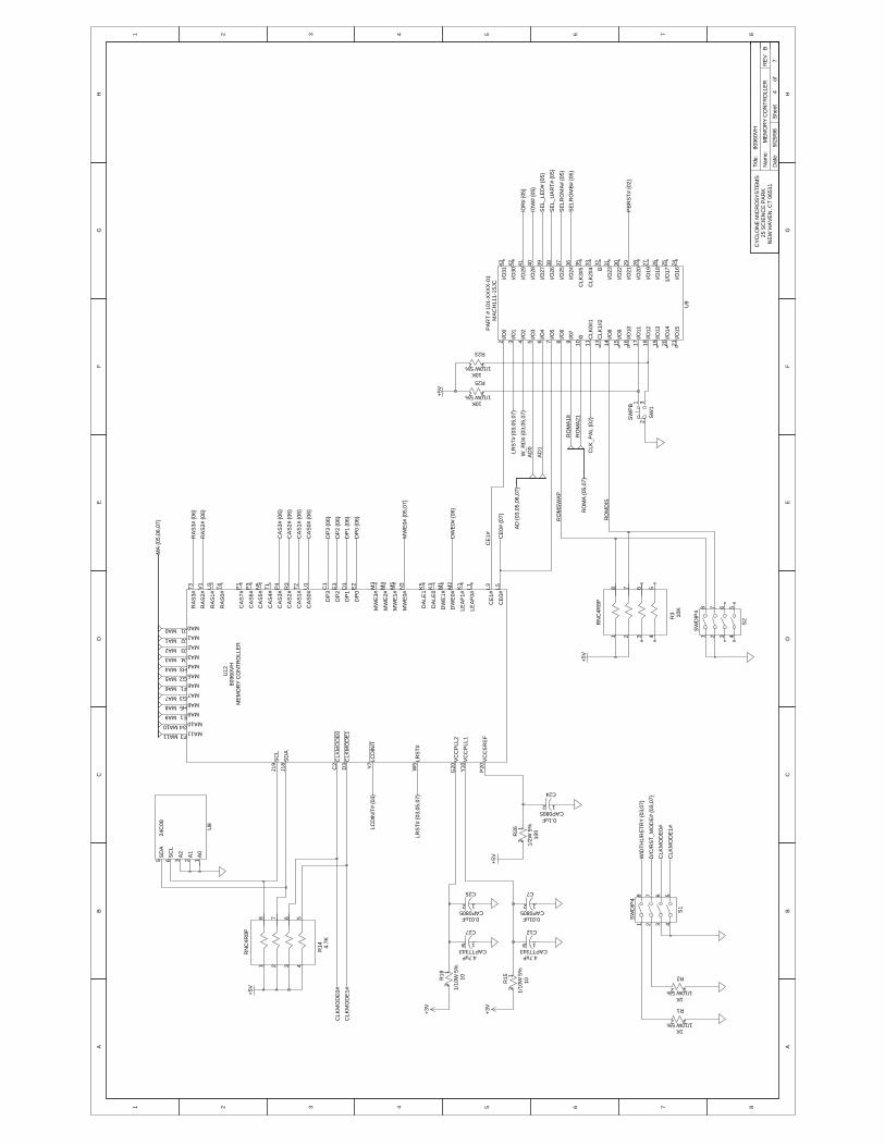
AB
CD
EF
GH
AB
CD
EF
GH
1 2 3 4 5 6 7 8
1 2 3 4 5 6 7 8
U9
MA
CH
111-
15JC
11C
LK0/
I133
CLK
2/I4
35C
LK3/
I5
9I/0
710
I0
32I3
251/
O17
13C
LK1/
I2
2I/O
03
I/O1
16I/O
1017
I/O11
18I/O
1219
I/O13
20I/O
1421
I/O15
24I/O
16
26I/O
18
27I/O
19
4I/O
2
28I/O
20
29I/O
21
30I/O
22
31I/O
23
36I/O
24
37I/O
25
38I/O
26
39I/O
27
40I/O
28
41I/O
295
I/O3
42I/O
30
43I/O
31
6I/O
47
I/O5
8I/O
6
14I/O
815
I/O9
R18
101/
10W
5%
12 R
15
101/
10W
5%
12
SW
1
SW
PB 1 3
2
ME
MO
RY
CO
NT
RO
LLE
R
U12
8096
0VH
C2
CLK
MO
DE
0D
3C
LKM
OD
E1
Y7
LCD
INIT
P20
VC
C5R
EF
Y10
VC
CP
LL1
G20
VC
CP
LL2
E2
DP
0
D1
DP
1
E3
DP
2
C1
DP
3
J19
SC
LJ1
8S
DA
U1
CA
S0#
T2
CA
S1#
R3
CA
S2#
P4
CA
S3#
T1
CA
S4#
N5
CA
S5#
P3
CA
S6#
P1
CA
S7#
L5C
E0#
L3C
E1#
K3
DA
LE0
K5
DA
LE1
M2
DW
E0#
M1
DW
E1#
L1LE
AF
0#
K1
LEA
F1#
W5
LRS
T#
J1 MA0
J2 MA1
G4 MA10
F3 MA11
J3 MA2
J4 MA3
H3 MA4
G2 MA5
F1 MA6
G3 MA7
H5 MA8
E1 MA9
N3
MW
E0#
M5
MW
E1#
M4
MW
E2#
M3
MW
E3#
T4
RA
S0#
U3
RA
S1#
V1
RA
S2#
T3
RA
S3#
S2
SW
DIP
41 2 3 4
8 7 6 5
S1
SW
DIP
41 2 3 4
8 7 6 5
C27
4.7uFCAPT7343
2 1
C12
4.7uFCAPT7343
2 1
U8
24C
08
1A
0
2A
1
3A
2
6S
CL
5S
DA
R3 10
K
RN
C4R
8P
8 7 6 54321
R2
1K1/10W 5% 12
R1
1K1/10W 5%
12
C25
0.01uFCAP0805
2 1
C7
0.01uFCAP0805
2 1
R26
100
1/2W
5%1
2
R23
10K1/10W 5%
12
R25
10K1/10W 5%
12
R14 4.
7K
RN
C4R
8P
8 7 6 54321
C24
0.1uFCAP0805
2 1
BR
EV
Titl
e:
Nam
e:
Dat
e:N
EW
HA
VE
N, C
T 0
6511
25 S
CIE
NC
E P
AR
KC
YC
LON
E M
ICR
OS
YS
TE
MS
She
etof
8096
0VH
9/29
/98
47
MA
{05
,06,
07}
MA11
MA10
MA9
MA8
MA7
MA6
MA5
MA4
MA3
MA2
MA1
MA0
RA
S3#
{06
}
RA
S2#
{06
}
+5V
CA
S3#
{06
}
CA
S2#
{06
}
CA
S1#
{06
}
CA
S0#
{06
}
DP
3 {0
6}
CLK
MO
DE
0#D
P2
{06}
CLK
MO
DE
1#D
P1
{06}
DP
0 {0
6}
LCD
INIT
# {0
3}
MW
E0#
{05
,07}
LRS
T#
{03,
05,0
7}
+3V
+5V
DW
E0#
{06
}
+3V
CE
1#+
5VC
E0#
{07
}
LRS
T#
{03,
05,0
7}A
D {
03,0
5,06
,07}
W_R
D#
{03,
05,0
7}IO
R#
{05}
AD
0IO
W#
{05}
AD
1S
EL_
LED
# {0
5}
SE
L_U
AR
T#
{05}
RO
MS
WA
PS
ELR
OM
A#
{05}
RO
MA
18S
ELR
OM
B#
{05}
RO
MA
21R
OM
A {0
5,07
}+
5VC
LK_P
AL
{02}
RO
MD
IS
PB
RS
T#
{02}
WID
TH
1/R
ET
RY
{03,
07}
D/C
/RS
T_M
OD
E#
{03,
07}
CLK
MO
DE
0#
CLK
MO
DE
1#
ME
MO
RY
CO
NT
RO
LLE
R
PA
RT
# 1
01-X
XX
X-0
1

AB
CD
EF
GH
AB
CD
EF
GH
1 2 3 4 5 6 7 8
1 2 3 4 5 6 7 8
U13
28F
020-
150
12A
0
11A
1
23A
10
25A
11
4A
12
28A
13
29A
14
3A
15
2A
16
30A
17
10A
2
9A
3
8A
4
7A
5
6A
6
5A
7
27A
8
26A
9
13D
0
14D
1
15D
2
17D
3
18D
4
19D
5
20D
6
21D
7
1V
PP
22C
E24
OE
31W
E
U14
E28
F01
6S5
24A
0
23A
1
14A
10
13A
11
8A
12
7A
13
6A
14
5A
15
4A
16
3A
17
2A
18
1A
19
22A
2
40A
20
21A
3
20A
4
19A
5
18A
6
17A
7
16A
8
15A
9
36R
Y/B
Y
11V
PP
9C
E37
OE
12R
P
38W
E
25D
0
26D
1
27D
2
28D
3
32D
4
33D
5
34D
6
35D
7
R4
470
1/10
W 5
%
12
R5
470
1/10
W 5
%
12
CR
2
LED
RE
D 21 C
R1
LED
GR
EE
N 21
U3
74A
LS04
1110
U3
74A
LS04
56
U3
74A
LS04
98
U3
74A
LS04
34
U3
74A
LS04
1312
U3
74A
LS04
12
CR3
LED4SM
2 1
CR3
LED4SM
8 7
CR3
LED4SM
6 5
CR3
LED4SM
4 3
CR4
LED4SM
8 7
CR4
LED4SM
6 5
CR4
LED4SM
2 1
CR4
LED4SM
4 3
R6470
RNC4R8P
8
7
6
5 4
3
2
1
R7470
RNC4R8P
8
7
6
5 4
3
2
1
U2
74A
BT
273
31D
42D
73D
84D
135D
146D
177D
188D
11C
LK1
CLR
21Q
52Q
63Q
94Q
125Q
156Q
167Q
198Q
U15
74A
BT
573
21D
32D
43D
54D
65D
76D
87D
98D
11LE
1O
C
191Q
182Q
173Q
164Q
155Q
146Q
137Q
128Q
J1
CO
NN
J6-6
P1 2 3 54 6
U5
OS
C1.
8432
MH
z
1E
/D5
O
U4
1488
2IN
1A
4IN
1B5
IN2B
9IN
3A10
IN3B
12IN
4A13
IN4B
3O
UT
A
6O
UT
B
8O
UT
C
11O
UT
D
U1
1489
A
13
12
11
U1
1489
A
10
9
8
U1
1489
A
1
2
3
U1
1489
A
4
5
6
U6
16C
550
31A
0
30A
1
29A
2
14C
S0
15C
S1
25IO
R
21IO
W39
RS
T
10R
XC
LK
11R
XD
18X
TA
L1
28A
S
42C
D
16C
S2
40C
TS
41D
SR
24IO
R
20IO
W
43R
I
2D
0
3D
1
4D
2
5D
3
6D
4
7D
5
8D
6
9D
7
33IN
T
32R
XR
DY
13T
XD
27T
XR
DY
19X
TA
L2
17B
AU
DO
UT
26D
DIS
37D
TR
38O
P1
35O
P2
36R
TS
BR
EV
Titl
e:
Nam
e:
Dat
e:N
EW
HA
VE
N, C
T 0
6511
25 S
CIE
NC
E P
AR
KC
YC
LON
E M
ICR
OS
YS
TE
MS
She
etof
8096
0VH
9/29
/98
57
+5V
AD
7
RO
MA
{04,
07}
AD
6
AD
5
AD
{03
,04,
06,0
7}A
D4
AD
3+
5VA
D2
AD
1
AD
21R
OM
A21
AD
0
AD
20R
OM
A20
MA
2
AD
19R
OM
A19
MA
1
AD
18R
OM
A18
MA
0
AD
17R
OM
A17
+5V
AD
16R
OM
A16
SE
L_U
AR
T#
{04}
AD
15R
OM
A15
AD
14R
OM
A14
ALE
{03
,07}
IOR
# {0
4}
IOW
# {0
4}
XIN
T5#
{03,
07}
MA
{04
,06,
07}
LRS
T#
{03,
04,0
7}
+5V
+5V
+12
V
RO
MA
20
RO
MA
17R
OM
A19
RO
MA
16R
OM
A18
RO
MA
15R
OM
A17
RO
MA
14R
OM
A16
AD
0LE
D0
MA
11R
OM
A15
AD
1LE
D1
MA
10R
OM
A14
AD
2LE
D2
MA
9M
A11
AD
3LE
D3
MA
8M
A10
AD
4LE
D4
MA
7M
A9
AD
5LE
D5
MA
6M
A8
AD
6LE
D6
MA
5A
D7
MA
7A
D7
LED
7
MA
4A
D6
MA
6S
EL_
LED
# {0
4}
LED7
LED6
LED5
LED4
LED3
LED2
LED1
LED0
MA
3A
D5
MA
5
MA
2A
D4
MA
4
MA
1A
D3
MA
3
MA
0A
D2
MA
2
AD
1M
A1
AD
7
AD
0M
A0
AD
6
AD
5
AD
4
SE
LRO
MA
# {0
4}A
D3
AD
2
SE
LRO
MB
# {0
4}A
D1
+5V
AD
0F
AIL
# {0
3}
+5V
DE
N#
{03,
07}
BE
1# {
03,0
7}B
E0#
{03
,07}
MW
E0#
{04
,07}
W_R
D#
{03,
04,0
7}N
ON
-VO
L M
EM
OR
Y
SP
AR
ES

AB
CD
EF
GH
AB
CD
EF
GH
1 2 3 4 5 6 7 8
1 2 3 4 5 6 7 8
J3
DR
AM
-SIM
M72
59+
5V
40C
AS
0
43C
AS
1
41C
AS
242
CA
S3
53D
10
55D
11
57D
12
61D
13
63D
14
65D
15
50D
24
52D
25
54D
26
56D
27
58D
28
60D
29
62D
30
64D
31
49D
8
51D
9
37D
P1
38D
P3
39G
ND
1
72G
ND
2
46N
C1
48N
C2
66N
C3
71N
C4
67P
D1
68P
D2
69P
D3
70P
D4
44R
AS
045
RA
S1
47W
E
J3
DR
AM
-SIM
M72
10+
5V1
30+
5V2
12A
013
A1
19A
10
14A
215
A3
16A
417
A5
18A
6
28A
7
31A
832
A9
2D
0
4D
1
3D
16
5D
17
7D
18
9D
19
6D
2
21D
20
23D
21
25D
22
27D
23
8D
3
20D
4
22D
5
24D
6
26D
7
36D
P0
35D
P2
1G
ND
11N
C1
29N
C2
34R
AS
2
33R
AS
3
R22
22
RN
C4R
8P
8 7 6 54321
R8 22
RN
C4R
8P
8 7 6 54321
R11
22
RN
C4R
8P
8 7 6 54321
R10
22
RN
C4R
8P
8 7 6 54321
R9 22
RN
C4R
8P
8 7 6 54321
BR
EV
Titl
e:
Nam
e:
Dat
e:N
EW
HA
VE
N, C
T 0
6511
25 S
CIE
NC
E P
AR
KC
YC
LON
E M
ICR
OS
YS
TE
MS
She
etof
8096
0VH
9/29
/98
67
MA
{04
,05,
07}
PM
A
MA
10P
MA
10+
5V+
5VM
A9
PM
A9
AD
{03
,04,
05,0
7}M
A8
PM
A8
DP
1 {0
4}A
D0
DP
3 {0
4}M
A7
PM
A7
AD
16
AD
1P
CA
S0#
AD
17P
CA
S2#
AD
2P
CA
S3#
AD
18P
CA
S1#
AD
3P
RA
S3#
MA
6P
MA
6A
D19
PR
AS
2#M
A5
PM
A5
MA
4P
MA
4P
DW
E0#
PM
A0
MA
3P
MA
3P
MA
1A
D8
PM
A2
AD
24
PM
A3
AD
9
PM
A4
AD
25
PM
A5
AD
10
PM
A6
AD
26M
A2
PM
A2
PM
A10
AD
11M
A1
PM
A1
AD
4A
D27
MA
0P
MA
0A
D20
AD
12
AD
5A
D28
AD
21
AD
6A
D29
AD
22A
D13
AD
7A
D30
PM
EM
AD
23A
D14
PM
A7
AD
31C
AS
3# {
04}
PC
AS
3#A
D15
CA
S2#
{04
}P
CA
S2#
CA
S1#
{04
}P
CA
S1#
PM
A8
PM
A9
CA
S0#
{04
}P
CA
S0#
PR
AS
2#
PR
AS
3#
DP
2 {0
4}
DP
0 {0
4}
RA
S2#
{04
}P
RA
S2#
RA
S3#
{04
}P
RA
S3#
DW
E0#
{04
}P
DW
E0#
DR
AM
SIM
M S
OC
KE
T

AB
CD
EF
GH
AB
CD
EF
GH
1 2 3 4 5 6 7 8
1 2 3 4 5 6 7 8
J8
HE
AD
ER
2X
251
10
1112
1314
1516
1718
19
2 20
2122
2324
2526
2728
293
30
3132
3334
3536
3738
39
4 40
4142
4344
4546
4748
495
506
78
9
J7
HE
AD
ER
2X
251
10
1112
1314
1516
1718
19
2 20
2122
2324
2526
2728
293
30
3132
3334
3536
3738
39
4 40
4142
4344
4546
4748
495
506
78
9
J6
MIC
TO
R
4 25 24 23 22 21 205 63C
LK0
36C
LK1
7 8 9 10
39G
ND
140
GN
D2
41G
ND
342
GN
D4
43G
ND
5
11 12 13 14 15 16 17 18 19 35 34 33 32 31 30 29 28 27 26
J4
MIC
TO
R
4 25 24 23 22 21 205 63C
LK0
36C
LK1
7 8 9 10
39G
ND
140
GN
D2
41G
ND
342
GN
D4
43G
ND
5
11 12 13 14 15 16 17 18 19 35 34 33 32 31 30 29 28 27 26
J5
MIC
TO
R
4 25 24 23 22 21 205 63C
LK0
36C
LK1
7 8 9 10
39G
ND
140
GN
D2
41G
ND
342
GN
D4
43G
ND
5
11 12 13 14 15 16 17 18 19 35 34 33 32 31 30 29 28 27 26
BR
EV
Titl
e:
Nam
e:
Dat
e:N
EW
HA
VE
N, C
T 0
6511
25 S
CIE
NC
E P
AR
KC
YC
LON
E M
ICR
OS
YS
TE
MS
She
etof
8096
0VH
9/29
/98
77
+5V
+5V
BE
0# {
03,0
5}B
E1#
{03
,05}
BE
3# {
03}
BE
2# {
03}
AD
S#
{03}
WID
TH
0 {0
3}
D/C
/RS
T_M
OD
E#
{03,
04}
WID
TH
1/R
ET
RY
{03,
04}
AD
{03
,04,
05,0
6}W
_RD
# {0
3,04
,05}
DT
/R {0
3}
BLA
ST
# {0
3}
RO
MA
{04,
05}
DE
N#
{03,
05}
MA
{04
,05,
06}
RD
YR
CV
# {0
3}LR
DY
RC
V#
{03}
HO
LD {0
3}
LOC
K#
{03}
CLK
_MIC
2 {0
2}C
LK_M
IC1
{02}
HO
LDA
{03
}X
INT
0# {0
3}R
OM
A15
AD
15LR
ST
# {0
3,04
,05}
XIN
T2#
{03}
RO
MA
14A
D14
LOC
K#
{03}
XIN
T1#
{03}
MA
11A
D13
LRD
YR
CV
# {0
3}X
INT
3# {0
3}X
INT
4# {0
3}M
A10
AD
12R
DY
RC
V#
{03}
XIN
T6#
{03}
MA
9A
D11
BLA
ST
# {0
3}X
INT
5# {0
3,05
}M
A8
AD
10D
EN
# {0
3,05
}X
INT
7# {0
3}N
MI#
{03}
MA
7A
D9
DT
/R {0
3}D
AC
K#
{03}
MA
6A
D8
W_R
D#
{03,
04,0
5}D
RE
Q#
{03}
MA
5A
D7
D/C
/RS
T_M
OD
E#
{03,
04}
WA
IT#
{03}
LRS
T#
{03,
04,0
5}M
A4
AD
6W
IDT
H1/
RE
TR
Y {0
3,04
}M
A3
AD
5W
IDT
H0
{03}
MA
2A
D4
AD
S#
{03}
MA
1A
D3
BE
3# {
03}
MA
0A
D2
BE
2# {
03}
BE
1# {
03,0
5}A
D1
BE
1# {
03,0
5}
BE
0# {
03,0
5}A
D0
BE
0# {
03,0
5}
LRS
T#
{03,
04,0
5}A
LE {
03,0
5}A
D {
03,0
4,05
,06}
W_R
D#
{03,
04,0
5}A
D31
MW
E0#
{04
,05}
AD
30
CE
0# {
04}
AD
29W
AIT
# {0
3}+
5V+
5V
AD
{03
,04,
05,0
6}A
D7
AD
28D
AC
K#
{03}
AD
0A
D1
AD
6A
D27
DR
EQ
# {0
3}A
D2
AD
5A
D26
HO
LDA
{03
}A
D3
AD
4A
D4
AD
25H
OLD
{03}
AD
5A
D3
AD
24N
MI#
{03}
AD
6A
D7
AD
2A
D23
XIN
T7#
{03}
AD
8A
D1
AD
22X
INT
6# {0
3}A
D9
AD
10A
D0
AD
21X
INT
5# {0
3,05
}A
D11
RO
MA
20A
D20
XIN
T4#
{03}
AD
12A
D13
RO
MA
19A
D19
XIN
T3#
{03}
AD
14R
OM
A18
AD
18X
INT
2# {0
3}A
D15
AD
16R
OM
A17
AD
17X
INT
1# {0
3}A
D17
RO
MA
16A
D16
XIN
T0#
{03}
AD
18A
D19
AD
20
AD
21A
D22
AD
23
AD
24A
D25
AD
26
AD
27A
D28
AD
29
AD
30A
D31
ALE
{03
,05}
CLK
_EX
P {
02}
LOG
IC A
NA
LYZ
ER
/EX
PA
NS
ION


PLD Code C
MODULE VH
TITLE ’VH’
" PATTERN 101-XXXX-01
" REVISION
" AUTHORJohn Neumann
" COMPANYCyclone Microsystems
" DATE June 10, 1998
" CHIP MACH111-15JC
CLK PIN 11; "pal clock input
CE1b PIN 2; "ROM space chip enable #1
RSTb PIN 3; "local reset
WRDb PIN 4; "write/read strobe
AD0 PIN 5; "address/data bit 0
AD1 PIN 6; "address/data bit 1
CE0b PIN 7; "ROM space chip enable #0
ROMSWAP PIN 8; "Select between EEPROM devices
ROMDIS PIN 14; "EEPROM ROM disable
RA18 PIN 9; "ROM address bit 18
RA21 PIN 10; "ROM address bit 21
RESET PIN 17; "Push Button reset
SET PIN 18; "Push Button set
PBRSTb PIN 29; "Debounce push button reset
QS0 PIN 43 ISTYPE ’REG_D’;"quickswitch mux select 0
QS1 PIN 42 ISTYPE ’REG_D’;"quickswitch mux select 1
IORb PIN 41 ISTYPE ’REG_D’; "UART read strobe
IOWb PIN 40 ISTYPE ’REG_D’;"UART write strobe
SELLEDb PIN 39 ISTYPE ’REG_D’;"LED chip enable
SELUARTbPIN 38 ISTYPE ’REG_D’;"UART chip enable
SELROMAbPIN 37 ISTYPE ’REG_D’;"Select for 28F020
SELROMBbPIN 36 ISTYPE ’REG_D’;"Select for 28F016S5
EQUATIONS
" Quickswitch mux selects for DRAM select, write to address E0200000h with data
QS0 := WRDb & RSTb & RA21 * !CE1b & AD0
# QS0 & !(RA21 & !CE1b) & RSTb"hold
# QS0 & !WRDb & RSTb & RA21 & !CE1b;"hold during a read
QS0.CLK = CLK;
QS1 := WRDb & RSTb & RA21 * !CE1b & AD1
# QS1 & !(RA21 & !CE1b) & RSTb"hold
# QS1 & !WRDb & RSTb & RA21 & !CE1b;"hold during a read
QS1.CLK = CLK;
" Select LED is write only to address E0040000h
!SELLEDb := RA18 & !RA21 & WRDb & !CE1b;
SELLEDb.CLK = CLK;
" The UART is located at address E0000000h
!SELUARTb := !RA18 & !RA21 & !CE1b;
SELUARTb.CLK = CLK;
" UART read and write strobes
!IORb := !WRDb & RSTb & !CE1b & !SELUARTb;
IORb.CLK = CLK;
EVAL80960VH Evaluation Platform Board Manual C-1

PLD Code
!IOWb := WRDb & RSTb & !CE1b & !SELUARTb;
IOWb.CLK = CLK;
" Flash ROM selects. Rom A is located at FEC0 0000H to FEC3 FFFFH.
" ROM B is located at FEE0 0000H TO FEFF FFFFH.
" The equations below allow ROM ’B’ and ROM ’A’ to be ’swapped’ thus
" changing the device from which the i960 boots.
!SELROMAb := ROMSWAP & !CE0b & !RA21 & ROMDIS
# !ROMSWAP & !CE0b & RA21 & ROMDIS;
SELROMAb.CLK = CLK;
!SELROMBb := ROMSWAP & !CE0b & RA21 & ROMDIS
# !ROMSWAP & !CE0b & !RA21 & ROMDIS;
SELROMBb.CLK = CLK;
"Push button reset must be debounce before it can be anded with PCI reset
!PBRSTb= !SET # (!PBRSTb & RESET);
END
C-2 EVAL80960VH Evaluation Platform Board Manual

Backplane 0015 Interface D
D.1 Introduction
The Backplane 0015 board from Cyclone Microsystems allows the EVAL80960VH platform to be installed into a PCI socket on the board and function as a host system board. The Backplane 0015 contains four PCI slots, J1 through J4. Figure D-1 depicts board component locations. The PCI backplane board contains a 33MHz bus clock, arbitration for the four PCI slots, an ATX power supply connector with stand-by voltage power on circuit, a reset circuit, and two LEDs indicating +5V and +3.3V availability.
D.2 Installing the EVAL80960VH into the Backplane 0015
The EVAL80960VH platform must be installed into slot J4 of the backplane board. The enclosed ribbon cable must be connected to allow proper function of the EVAL80960VH as a host board. Please refer to Figure D-2 and Figure D-3 during installation and setup. Install the 26 pin keyed connector into the header position, J5, on the backplane board. The red wire should line up with pin 1 of J5. Next install the other end of the ribbon cable into J7 on the EVAL80960VH. Take care as this connector does not have any keying associated with it. The red wire should line up with pin 50 on J7, towards the top edge of the platform. This cable allows interrupts from the PCI slots on the backplane board to reach the i960VH processor.
D.3 Powering the EVAL80960VH/Backplane System
The PCI backplane board is designed to be powered via an ATX power supply. Before inserting the power cable into the ATX power connector on the backplane board make sure that the +5VSB (stand-by voltage) is off. Inserting the power cable with +5VSB on may cause damage to the start up circuit and the backplane board may not power up. After the connector is installed, depress the momentary power switch to turn on the +5V and +3.3V rails on the ATX power supply.
EVAL80960VH Evaluation Platform Board Manual D-1

Backplane 0015 Interface
D.4 Interrupt Routing and IDSELs on the Backplane 0015
The PCI slots J1 through J3 allow up to 3 adapter boards to be installed in the system. These adapter boards are configured by the EVAL80960VH and interrupt the i960VH processor through the ribbon cable. The interrupt routing and IDSELs on the backplane board is shown in Table D-1. Note that the EVAL80960VH has the ability to interrupt itself.
Table D-1. PCI Interrupt Routing and IDSELs
SLOT INTA INTB INTC INTD IDSEL
J1 XINT1 XINT2 XINT3 XINT0 AD16
J2 XINT2 XINT3 XINT0 XINT1 AD17
J3 XINT3 XINT0 XINT1 XINT2 AD18
J4 XINT0 XINT1 XINT2 XINT3 AD19
Figure D-1. EVAL80960VH Backplane Board Illustration
U2
U1
J6
J4
J3
J2
J1
J5
33 MHz Oscillator
PCI Slot for EVAL80960VH
Connector to EVAL80960VH
Power Switch
Reset Switch
ATX Power Supply Connector
PCI Bus Arbitration PAL
D-2 EVAL80960VH Evaluation Platform Board Manual

Backplane 0015 Interface
Figure D-2. EVAL80960VH/Backplane 0015 with Eval Board Installed
Figure D-3. EVAL80960VH/Backplane 0015 Installation
EVAL80960VH Evaluation Platform Board Manual D-3

Backplane 0015 Interface
the t to
not
n the ,
re
ns
f a
D.5 PCI Host Detection and Configuration
When installed in the slot J4 of the backplane, the EVAL80960VH acts as the PCI host in the system. The EVAL80960VH determines whether it is in the host state by the XINT4 input. The backplane drives the VH processor’s XINT4 low via the ribbon cable. Upon system startup, MON960 uses the presence of an XINT4 interrupt to determine whether it needs to initialize primary PCI bus. If the EVAL80960VH is the PCI host, the ATU base address (PIABAR) is sethe base of DRAM (A000 0000h), and the master enable bit in the ATU command register (PATUCMD) is set. MON960 then disables XINT4. Users should be aware that XINT4 shouldbe enabled.
D.6 PCI Initialization
When acting as a PCI host, MON960 extensions are responsible for initializing the devices oPCI bus of the EVAL80960VH. PCI initialization involves allocating address spaces (MemoryMemory Mapped I/O, and I/O), assigning PCI base addresses, assigning IRQ values (seeTable D-1), and enabling PCI mastership. Devices containing PCI-to-PCI bridges and hierarchical buses are not supported.
D.7 PCI Bios Routines
The PCI BIOS routines are accessible at the MON960 layer and can also be accessed by application level software by using the i960 system call mechanism and the System ProceduTable. The supported BIOS functions are described in the subsections that follow.
pci_bios_present()
find_pci_device()
find_pci_class_code()
generate_special_cycle()
read_config_byte()
read_config_word()
read_config_dword()
write_config_byte()
write_config_word()
write_config_dword()
get_irq_routing_options()
set_pci_irq()
Although the calling interface is different from that used on a DOS-based host, these functiopreserve, as closely as possible, the parameters and return values described in PCI Local Bus Specification, Revision 2.1. Functions that return multiple values do so by filling in the fields ostructure passed by the calling routine.
pci_bios_present
D-4 EVAL80960VH Evaluation Platform Board Manual

Backplane 0015 Interface
until at
D if l.
ass ber of
s to urns
This function allows the caller to determine whether the PCI BIOS interface function set is present, and the current interface version level. It also provides information about the hardware mechanism used for accessing configuration space and whether or not the hardware supports generation of PCI Special Cycles.
Calling convention:
int pci_bios_present (
PCI_BIOS_INFO *info
);
Return values:
This function always returns SUCCESSFUL.
find_pci_device
This function returns the location of PCI devices that have a specific Device ID and Vendor ID. Given a Vendor ID, a Device ID, and an Index, the function returns the Bus Number, Device Number, and Function Number of the Nth Device/Function whose Vendor ID and Device ID match the input parameters.
Calling software can find all devices having the same Vendor ID and Device ID by making successive calls to this function starting with the index set to “0”, and incrementing the indexthe function returns DEVICE_NOT_FOUND. A return value of BAD_VENDOR_ID indicates ththe Vendor ID value passed had a value of all “1”s.
Calling convention:int find_pci_device (
int device_id,
int vendor_id,
int index
);
Return values:
This function returns SUCCESSFUL if the indicated device is located, DEVICE_NOT_FOUNthe indicated device cannot be located, or BAD_VENDOR_ID if the vendor_id value is illega
find_pci_class_code
This function returns the location of PCI devices that have a specific Class Code. Given a ClCode and an Index, the function returns the Bus Number, Device Number, and Function Numthe Nth Device/Function whose Class Code matches the input parameters.
Calling software can find all devices having the same Class Code by making successive callthis function starting with the index set to “0”, and incrementing the index until the function retDEVICE_NOT_FOUND.
Calling convention:int find_pci_class_code (
int class_code,
int index
);
EVAL80960VH Evaluation Platform Board Manual D-5

Backplane 0015 Interface
Return values:
This function returns SUCCESSFUL if the indicated device is located or DEVICE_NOT_FOUND if the indicated device cannot be located.
generate_special_cycle
This function allows for generation of PCI Special Cycles. The generated special cycle is broadcast on a specific PCI Bus in the system.
PCI Special Cycles are not supported on the 0015 backplane PCI bus.
Calling convention:int generate_special_cycle (
int bus_number,
int special_cycle_data
);
Return values:
Since PCI Special Cycles are not supported by the 0015 backplane, this function always returns FUNC_NOT_SUPPORTED.
read_config_byte
This function allows the caller to read individual bytes from the configuration space of a specific device.
Calling convention:int read_config_byte (
int bus_number,
int device_number,
int function_number,
int register_number,/* 0,1,2,...,255 */
UINT 8*data
);
Return values:
This function returns SUCCESSFUL if the indicated byte was read correctly or ERROR if there is a problem with the parameters.
read_config_word
This function allows the caller to read individual shorts (16 bits) from the configuration space of a specific device. The Register Number parameter must be a multiple of two (i.e., bit 0 must be set to “0”).
Calling convention:int read_config_word (
int bus_number,
int device_number,
int function_number,
int register_number,/* 0,2,4,...,254 */
D-6 EVAL80960VH Evaluation Platform Board Manual

Backplane 0015 Interface
re is
c
ere
f a set to
UINT 16*data
);
Return values:
This function returns SUCCESSFUL if the indicated word was read correctly or ERROR if there is a problem with the parameters.
read_config_dword
This function allows the caller to read individual longs (32 bits) from the configuration space of a specific device. The Register Number parameter must be a multiple of four (i.e., bits 0 and 1 must be set to “0”).
Calling convention:int read_config_dword (
int bus_number,
int device_number,
int function_number,
int register_number,/* 0,4,8,...,252 */
UINT 32*data
);
Return values:
This function returns SUCCESSFUL if the indicated long was read correctly or ERROR if thea problem with the parameters.
write_config_byte
This function allows the caller to write individual bytes to the configuration space of a specifidevice.
Calling convention:int write_config_byte (
int bus_number,
int device_number,
int function_number,
int register_number,/* 0,1,2,...,255 */
UINT 8*data
);
Return values:
This function returns SUCCESSFUL if the indicated byte was written correctly or ERROR if this a problem with the parameters.
write_config_word
This function allows the caller to write individual shorts (16 bits) to the configuration space ospecific device. The Register Number parameter must be a multiple of two (i.e., bit 0 must be“0”).
Calling convention:
EVAL80960VH Evaluation Platform Board Manual D-7

Backplane 0015 Interface
ere
alues shows e
int write_config_word (
int bus_number,
int device_number,
int function_number,
int register_number,/* 0,2,4,...,254 */
UINT 16*data
);
Return values:
This function returns SUCCESSFUL if the indicated word was written correctly or ERROR if there is a problem with the parameters.
write_config_dword
This function allows the caller to write individual longs (32 bits) to the configuration space of a specific device. The Register Number parameter must be a multiple of four (i.e., bits 0 and 1 must be set to “0”).
Calling convention:int write_config_dword (
int bus_number,
int device_number,
int function_number,
int register_number,/* 0,4,8,...,252 */
UINT 32*data
);
Return values:
This function returns SUCCESSFUL if the indicated long was written correctly or ERROR if this a problem with the parameters.
get_irq_routing_options
This routine returns the PCI interrupt routing options available on the 0015 backplane. Two vare provided for each PCI interrupt pin for each device. One of these values is a bitmap that the interrupt to which 80960VH XINT (XINT3:0) is connected. The second value is a link valuthat provides a way of specifying which PCI interrupt pins are wire-OR’ed together on the motherboard. Interrupt pins with the same link value are wired together.
The PCI Interrupt routing fabric on the 0015 backplane is not reconfigurable (fixed mapping relationships).
Calling convention:int get_irq_routing_options (
PCI_IRQ_ROUTING_TABLE *table
);
Return values:
This function always returns SUCCESSFUL.
set_pci_irq
D-8 EVAL80960VH Evaluation Platform Board Manual

Backplane 0015 Interface
The PCI Interrupt routing fabric on the 0015 backplane is not reconfigurable (fixed mapping relationships); therefore, this function is not supported.
Calling convention:int set_pci_irq (
int int_pin,
int irq_num,
int bus_dev
);
Return values:
This function always returns FUNC_NOT_SUPPORTED.
D.8 Additional MON960 Commands
The following commands have been added to the UI interface of MON960 to support the 0015 backplane.
print_pci Utility
A print_pci command to MON960 is accessed through the MON960 command prompt. This command displays the contents of the PCI configuration space on a selected adapter on the primary PCI interface or on the i960 VH processor itself. For more information on the meaning of the fields in PCI configuration space, refer to the PCI Local Bus Specification Revision 2.1. The syntax of this command is:
pp <bus number> <device number> <function number>
D.9 Bill of Material
This appendix identifies all components on the Backplane 0015 Interface (Table D-2).
Table D-2. Backplane 0015 Interface Bill of Material (Sheet 1 of 3)
Cyclone P/N Reference Designator Description Qty Mfg Mfg Part Number Note
100-1698 U7 IC/SM 74HC74 SOIC-14 1 Texas Instruments SN74HC74D
100-1699 U5 IC/SM 74HC14 SOIC 1 National Semi. 74HC14
100-1225 U4 IC/SM 74AS760 SOIC 1 Texas Instruments SN74AS760DW
100-2200 U6 IC/SM TL7705ACD 1 Texas Instruments TL7705ACD
100-3098 U3 IC/SM LVCMOS Fanout Buffr SSOP 1 Motorola MPC9140
110-3209 C16,C31 CAP TANT SM 47uf, 16V (7343) 2 AVX TPSD476K016R015 (2)
EVAL80960VH Evaluation Platform Board Manual D-9

Backplane 0015 Interface
110-3210 C38 CAP TANT SM 33uf, 10V (7343) 1 Sprague 293D336X9016D2T (2)
110-3214 C35 CAP TANT SM 10uf 25/35V (7343) 1 Sprague 293D1060025D2
T (2)
110-3301 C8-C15,C18-C25 CAP CERM SM, 0.01uf (0805) 16 (1)
110-3304
C1-C7,C17, C26-C30,C32-
C34, C36,C37
CAP CERM SM, 0.1uf (0805) 18 (1)
126-0000-05 R21 R/SM 1/10W 5% 000 ohm (0805) 1 (1)
126-1004-05 R5,R13-R20,R22,R24 R/SM 1/10W 5% 10K ohm (0805) 11 (1)
126-2703-05 R6,R23,R25 R/SM 1/10W 5% 2.7k ohm (0805) 3 (1)
126-3301-05 R1,R9 R/SM 1/10W 5% 33 ohm (0805) 2 (1)
126-3302-05 R4 R/SM 1/10W 5% 330 ohm (0805) 1 (1)
126-4702-05 R3 R/SM 1/10W 5% 470 ohm (0805) 1 (1)
129-2101 R2,R10-R12 Resistor Pk SM RNC4R8P 2.7kohm 4 CTS 742083272JTR (2)
129-2105 R7 Resistor Pk SM RNC4R8P 4.7kohm 1 CTS 742083472JTR (2)
129-2113 R8 Resistor Pk SM RNC4R8P 33 ohm 1 CTS 742083330JTR (2)
129-2102 R301 Resistor Pk SM 10K ohm 1 CTS 7420B3103JTR
130-1460 J1-J4 CONN PCI SLOT 5V/PCB thru hole 4 AMP 145154-4
130-1519 J6 CONN PCPWR Male /Mini-Fit/20p 1 Molex 39-29-9202
130-1580 J5 CONN Hdr 26 pin/w shell, PCB 1 AMP 104339-6
130-1621 Z1,Z2 Jumper JUMP2X1 2 Molex 22-28-4023
150-4000 SW1,SW2 Switch, SW-PUSH 3P (Right Ang) 2 C&K Switch EP12SD1ABE
150-6013 U1 OSC 33.0 MHz Half 1 Ecliptek ECI900HS33.000M
150-9100 CR1,CR2 LED Green 2 Hewlett Packard HLMP-3507$010
160-1108 CR3 Diode SM BAS16 1 National Semi. BAS16 (2)
193-2002 U2 SOCKET PLCC44 LP Surface Mount 1 AMP 822275-1
230-1197 MT1-MT4 SCREW-NYLON 4/40x3/8" Pan Slot 4 McMaster
Carr 95000A108 (3)
230-1507 MT1-MT4 HARDWARE 4-40 x 3/8" Standoff 4 Keystone 1902B (0.375") (3)
270-0015 PCB 0015A / VH Extender 1
Note (1) - Provided by assembly house by specified description
Table D-2. Backplane 0015 Interface Bill of Material (Sheet 2 of 3)
Cyclone P/N Reference Designator Description Qty Mfg Mfg Part Number Note
D-10 EVAL80960VH Evaluation Platform Board Manual
Backplane 0015 Interface
D.10 Schematics
Note (2) - Provided by Cyclone - stocked at assembly house
Note (3) - Reference assembly drawing
Note (4) - Pre-programmed device
Table D-2. Backplane 0015 Interface Bill of Material (Sheet 3 of 3)
Cyclone P/N Reference Designator Description Qty Mfg Mfg Part Number Note
EVAL80960VH Evaluation Platform Board Manual D-11


AB
CD
EF
GH
AB
CD
EF
GH
1 2 3 4 5 6 7 8
1 2 3 4 5 6 7 8
R12 2.
7K
RN
C4R
8P
8 7 6 54321
R2
2.7K
RN
C4R
8P
8 7 6 54321
R10 2.
7K
RN
C4R
8P
8 7 6 54321
R11 2.
7K
RN
C4R
8P
8 7 6 54321
R7
4.7K
RN
C4R
8P
8 7 6 54321
R17
10K
1/10
W 5
%
12
R16
10K
1/10
W 5
%
12
R13
10K
1/10
W 5
%
12
R15
10K
1/10
W 5
%
12
J2
CO
NN
PC
I_S
LOT
5V
A33
+3V
1
A39
+3V
2
A45
+3V
3
A53
+3V
4
B36
+3V
5
B41
+3V
6
B43
+3V
7
B54
+3V
8
A59
+5V
1
A61
+5V
2A
62+
5V3
B59
+5V
4
B61
+5V
5B
62+
5V6
B60
AC
K64
A52
C/B
E0
B44
C/B
E1
B33
C/B
E2
B37
DE
VS
EL
A34
FR
AM
EB
35IR
DY
B39
LOC
KB
40P
ER
R
A60
RE
Q64
A41
SB
OB
42S
ER
R
A38
ST
OP
A36
TRD
Y
A58
AD
00B
58A
D01
A57
AD
02
B56
AD
03
A55
AD
04B
55A
D05
A54
AD
06
B53
AD
07
B52
AD
08
A49
AD
09
B48
AD
10
A47
AD
11B
47A
D12
A46
AD
13
B45
AD
14
A44
AD
15
A32
AD
16B
32A
D17
A35
GN
D1
B57
GN
D10
A37
GN
D2
A42
GN
D3
A48
GN
D4
A56
GN
D5
B34
GN
D6
B38
GN
D7
B46
GN
D8
B49
GN
D9
A43
PA
R
A40
SD
ON
E
J1
CO
NN
PC
I_S
LOT
5V
A33
+3V
1
A39
+3V
2
A45
+3V
3
A53
+3V
4
B36
+3V
5
B41
+3V
6
B43
+3V
7
B54
+3V
8
A59
+5V
1
A61
+5V
2A
62+
5V3
B59
+5V
4
B61
+5V
5B
62+
5V6
B60
AC
K64
A52
C/B
E0
B44
C/B
E1
B33
C/B
E2
B37
DE
VS
EL
A34
FR
AM
EB
35IR
DY
B39
LOC
KB
40P
ER
R
A60
RE
Q64
A41
SB
OB
42S
ER
R
A38
ST
OP
A36
TRD
Y
A58
AD
00B
58A
D01
A57
AD
02
B56
AD
03
A55
AD
04B
55A
D05
A54
AD
06
B53
AD
07
B52
AD
08
A49
AD
09
B48
AD
10
A47
AD
11B
47A
D12
A46
AD
13
B45
AD
14
A44
AD
15
A32
AD
16B
32A
D17
A35
GN
D1
B57
GN
D10
A37
GN
D2
A42
GN
D3
A48
GN
D4
A56
GN
D5
B34
GN
D6
B38
GN
D7
B46
GN
D8
B49
GN
D9
A43
PA
R
A40
SD
ON
E
J2
CO
NN
PC
I_S
LOT
5V
A2
+12
V
A21
+3V
1
A27
+3V
2
B25
+3V
3
B31
+3V
4
A5
+5V
1
A8
+5V
2
A10
+5V
3
A16
+5V
4
B5
+5V
5B
6+
5V6
B19
+5V
7
B1
-12V
B26
C/B
E3
A17
GN
T
A6
INTA
B7
INTB
A7
INTC
B8
INTD
B9
PR
SN
T1
B11
PR
SN
T2
B18
RE
Q
A15
RS
T
A1
TR
ST
A31
AD
18
B30
AD
19
A29
AD
20B
29A
D21
A28
AD
22
B27
AD
23
A25
AD
24
B24
AD
25
A23
AD
26B
23A
D27
A22
AD
28
B21
AD
29
A20
AD
30B
20A
D31
B16
CLK
A12
GN
D1
B17
GN
D10
B22
GN
D11
B28
GN
D12
A13
GN
D2
A18
GN
D3
A24
GN
D4
A30
GN
D5
B3
GN
D6
B12
GN
D7
B13
GN
D8
B15
GN
D9
A26
IDS
EL
A9
A11
A14
A19
B10
B14B
2T
CK
A4
TDI
B4
TD
O
A3
TM
S
J1
CO
NN
PC
I_S
LOT
5V
A2
+12
V
A21
+3V
1
A27
+3V
2
B25
+3V
3
B31
+3V
4
A5
+5V
1
A8
+5V
2
A10
+5V
3
A16
+5V
4
B5
+5V
5B
6+
5V6
B19
+5V
7
B1
-12V
B26
C/B
E3
A17
GN
T
A6
INTA
B7
INTB
A7
INTC
B8
INTD
B9
PR
SN
T1
B11
PR
SN
T2
B18
RE
Q
A15
RS
T
A1
TR
ST
A31
AD
18
B30
AD
19
A29
AD
20B
29A
D21
A28
AD
22
B27
AD
23
A25
AD
24
B24
AD
25
A23
AD
26B
23A
D27
A22
AD
28
B21
AD
29
A20
AD
30B
20A
D31
B16
CLK
A12
GN
D1
B17
GN
D10
B22
GN
D11
B28
GN
D12
A13
GN
D2
A18
GN
D3
A24
GN
D4
A30
GN
D5
B3
GN
D6
B12
GN
D7
B13
GN
D8
B15
GN
D9
A26
IDS
EL
A9
A11
A14
A19
B10
B14B
2T
CK
A4
TDI
B4
TD
O
A3
TM
S
C13
0.01
uFC
AP
0805
21C9
0.01
uFC
AP
0805
21
C12
0.01
uFC
AP
0805
21
C8
0.01
uFC
AP
0805
21
BR
EV
Titl
e:
Nam
e:
Dat
e:N
EW
HA
VE
N, C
T 0
6511
25 S
CIE
NC
E P
AR
KC
YC
LON
E M
ICR
OS
YS
TE
MS
She
etof
015
11/1
9/98
13
PC
I {02
,03}
+5V
+3V
+5V
+5V
+3V
+12
V+
3V+
5V+
5V+
3V+
12V
PT
RS
T#
PT
RS
T#
PT
DI
PT
CK
PT
CK
PT
MS
N12
VP
TM
SN
12V
PT
MS
PT
CK
PT
DI
PT
DI
PT
RS
T#
INT
B#
{02,
03}
INT
C#
{02,
03}
INT
C#
{02,
03}
INT
D#
{02,
03}
INT
D#
{02,
03}
INT
A#
{02,
03}
INT
A#
{02,
03}
INT
B#
{02,
03}
+5V
PD
EV
SE
L#
PR
ST
#P
RS
T#
PT
RD
Y#
PC
LKA
{03
}P
CLK
B {
03}
PIR
DY
#P
GN
T0#
PG
NT
1#
PR
EQ
0#P
RE
Q1#
PF
RA
ME
#
PA
D31
PA
D30
PA
D31
PA
D30
PA
D29
PA
D29
PA
D28
PA
D28
PA
D27
PA
D26
PA
D27
PA
D26
PA
D25
PA
D25
PS
DO
NE
PA
D24
PA
D24
PP
ER
R#
PC
/BE
3#P
AD
16P
C/B
E3#
PA
D17
PLO
CK
#P
AD
23P
AD
23
PA
D22
PA
D22
PS
TO
P#
PA
D21
PA
D20
PA
D21
PA
D20
PA
D19
PA
D19
PA
D18
PA
D18
PA
D17
PA
D16
PA
D17
PA
D16
PR
EQ
1#P
C/B
E2#
PC
/BE
2#
PF
RA
ME
#P
FR
AM
E#
PR
EQ
1#
PIR
DY
#P
IRD
Y#
PR
EQ
0#P
TR
DY
#P
TR
DY
#P
RE
Q3#
PD
EV
SE
L#P
DE
VS
EL#
PS
TO
P#
PS
TO
P#
PLO
CK
#P
LOC
K#
PP
ER
R#
PS
DO
NE
PP
ER
R#
PS
DO
NE
PS
BO
#P
SB
O#
PS
ER
R#
PS
ER
R#
PS
BO
#P
PA
RP
PA
RP
SE
RR
#P
C/B
E1#
PA
D15
PC
/BE
1#P
AD
15
PA
D14
PA
D14
PA
D13
PA
D13
PA
D12
PA
D11
PA
D12
PA
D11
PA
D10
PA
D10
PA
D9
PA
D9
PA
D8
PC
/BE
0#P
AD
8P
C/B
E0#
PA
D7
PA
D7
PA
D6
PA
D6
PA
D5
PA
D4
PA
D5
PA
D4
PA
D3
PA
D3
PA
D2
PA
D2
PA
D1
PA
D0
PA
D1
PA
D0
+5V
+5V
+5V
PC
I BU
S 1
PC
I BU
S 2
PC
I BU
S 1
& 2

AB
CD
EF
GH
AB
CD
EF
GH
1 2 3 4 5 6 7 8
1 2 3 4 5 6 7 8
R19
10K
1/10
W 5
%
12
R18
10K
1/10
W 5
%
12
R14
10K
1/10
W 5
%
12
R20
10K
1/10
W 5
%
12
J4
CO
NN
PC
I_S
LOT
5V
A33
+3V
1
A39
+3V
2
A45
+3V
3
A53
+3V
4
B36
+3V
5
B41
+3V
6
B43
+3V
7
B54
+3V
8
A59
+5V
1
A61
+5V
2A
62+
5V3
B59
+5V
4
B61
+5V
5B
62+
5V6
B60
AC
K64
A52
C/B
E0
B44
C/B
E1
B33
C/B
E2
B37
DE
VS
EL
A34
FR
AM
EB
35IR
DY
B39
LOC
KB
40P
ER
R
A60
RE
Q64
A41
SB
OB
42S
ER
R
A38
ST
OP
A36
TRD
Y
A58
AD
00B
58A
D01
A57
AD
02
B56
AD
03
A55
AD
04B
55A
D05
A54
AD
06
B53
AD
07
B52
AD
08
A49
AD
09
B48
AD
10
A47
AD
11B
47A
D12
A46
AD
13
B45
AD
14
A44
AD
15
A32
AD
16B
32A
D17
A35
GN
D1
B57
GN
D10
A37
GN
D2
A42
GN
D3
A48
GN
D4
A56
GN
D5
B34
GN
D6
B38
GN
D7
B46
GN
D8
B49
GN
D9
A43
PA
R
A40
SD
ON
E
J3
CO
NN
PC
I_S
LOT
5V
A33
+3V
1
A39
+3V
2
A45
+3V
3
A53
+3V
4
B36
+3V
5
B41
+3V
6
B43
+3V
7
B54
+3V
8
A59
+5V
1
A61
+5V
2A
62+
5V3
B59
+5V
4
B61
+5V
5B
62+
5V6
B60
AC
K64
A52
C/B
E0
B44
C/B
E1
B33
C/B
E2
B37
DE
VS
EL
A34
FR
AM
EB
35IR
DY
B39
LOC
KB
40P
ER
R
A60
RE
Q64
A41
SB
OB
42S
ER
R
A38
ST
OP
A36
TRD
Y
A58
AD
00B
58A
D01
A57
AD
02
B56
AD
03
A55
AD
04B
55A
D05
A54
AD
06
B53
AD
07
B52
AD
08
A49
AD
09
B48
AD
10
A47
AD
11B
47A
D12
A46
AD
13
B45
AD
14
A44
AD
15
A32
AD
16B
32A
D17
A35
GN
D1
B57
GN
D10
A37
GN
D2
A42
GN
D3
A48
GN
D4
A56
GN
D5
B34
GN
D6
B38
GN
D7
B46
GN
D8
B49
GN
D9
A43
PA
R
A40
SD
ON
E
J4
CO
NN
PC
I_S
LOT
5V
A2
+12
V
A21
+3V
1
A27
+3V
2
B25
+3V
3
B31
+3V
4
A5
+5V
1
A8
+5V
2
A10
+5V
3
A16
+5V
4
B5
+5V
5B
6+
5V6
B19
+5V
7
B1
-12V
B26
C/B
E3
A17
GN
T
A6
INTA
B7
INTB
A7
INTC
B8
INTD
B9
PR
SN
T1
B11
PR
SN
T2
B18
RE
Q
A15
RS
T
A1
TR
ST
A31
AD
18
B30
AD
19
A29
AD
20B
29A
D21
A28
AD
22
B27
AD
23
A25
AD
24
B24
AD
25
A23
AD
26B
23A
D27
A22
AD
28
B21
AD
29
A20
AD
30B
20A
D31
B16
CLK
A12
GN
D1
B17
GN
D10
B22
GN
D11
B28
GN
D12
A13
GN
D2
A18
GN
D3
A24
GN
D4
A30
GN
D5
B3
GN
D6
B12
GN
D7
B13
GN
D8
B15
GN
D9
A26
IDS
EL
A9
A11
A14
A19
B10
B14B2
TC
K
A4
TDI
B4
TD
O
A3
TM
S
J3
CO
NN
PC
I_S
LOT
5V
A2
+12
V
A21
+3V
1
A27
+3V
2
B25
+3V
3
B31
+3V
4
A5
+5V
1
A8
+5V
2
A10
+5V
3
A16
+5V
4
B5
+5V
5B
6+
5V6
B19
+5V
7
B1
-12V
B26
C/B
E3
A17
GN
T
A6
INTA
B7
INTB
A7
INTC
B8
INTD
B9
PR
SN
T1
B11
PR
SN
T2
B18
RE
Q
A15
RS
T
A1
TR
ST
A31
AD
18
B30
AD
19
A29
AD
20B
29A
D21
A28
AD
22
B27
AD
23
A25
AD
24
B24
AD
25
A23
AD
26B
23A
D27
A22
AD
28
B21
AD
29
A20
AD
30B
20A
D31
B16
CLK
A12
GN
D1
B17
GN
D10
B22
GN
D11
B28
GN
D12
A13
GN
D2
A18
GN
D3
A24
GN
D4
A30
GN
D5
B3
GN
D6
B12
GN
D7
B13
GN
D8
B15
GN
D9
A26
IDS
EL
A9
A11
A14
A19
B10
B14B2
TC
K
A4
TDI
B4
TD
O
A3
TM
S
C15
0.01
uFC
AP
0805
21
C11
0.01
uFC
AP
0805
21
C14
0.01
uFC
AP
0805
21
C10
0.01
uFC
AP
0805
21
BR
EV
Titl
e:
Nam
e:
Dat
e:N
EW
HA
VE
N, C
T 0
6511
25 S
CIE
NC
E P
AR
KC
YC
LON
E M
ICR
OS
YS
TE
MS
She
etof
015
11/1
9/98
23
PC
I {01
,03}
+3V
+5V
+5V
+3V
+12
V+
3V+
5V+
5V+
3V+
12V
PT
RS
T#
PT
RS
T#
PT
CK
PT
CK
N12
VP
TM
SN
12V
PT
MS
PT
DI
PT
DI
INT
D#
{01,
03}
INT
A#
{01,
03}
INT
A#
{01,
03}
INT
B#
{01,
03}
INT
B#
{01,
03}
INT
C#
{01,
03}
INT
C#
{01,
03}
INT
D#
{01,
03}
PR
ST
#P
RS
T#
PC
LKC
{03
}P
CLK
D {
03}
PG
NT
2#P
GN
T3#
PR
EQ
2#P
RE
Q3#
PA
D31
PA
D30
PA
D31
PA
D30
PA
D29
PA
D29
PA
D28
PA
D28
PA
D27
PA
D26
PA
D27
PA
D26
PA
D25
PA
D25
PA
D24
PA
D24
PC
/BE
3#P
AD
18P
C/B
E3#
PA
D19
PA
D23
PA
D23
PA
D22
PA
D22
PA
D21
PA
D20
PA
D21
PA
D20
PA
D19
PA
D19
PA
D18
PA
D18
PA
D17
PA
D16
PA
D17
PA
D16
PC
/BE
2#P
C/B
E2#
PF
RA
ME
#P
FR
AM
E#
PIR
DY
#P
IRD
Y#
PT
RD
Y#
PT
RD
Y#
PD
EV
SE
L#P
DE
VS
EL#
PS
TO
P#
PS
TO
P#
PLO
CK
#P
LOC
K#
PP
ER
R#
PS
DO
NE
PP
ER
R#
PS
DO
NE
PS
BO
#P
SB
O#
PS
ER
R#
PS
ER
R#
PP
AR
PP
AR
PC
/BE
1#P
AD
15P
C/B
E1#
PA
D15
PA
D14
PA
D14
PA
D13
PA
D13
PA
D12
PA
D11
PA
D12
PA
D11
PA
D10
PA
D10
PA
D9
PA
D9
PA
D8
PC
/BE
0#P
AD
8P
C/B
E0#
PA
D7
PA
D7
PA
D6
PA
D6
PA
D5
PA
D4
PA
D5
PA
D4
PA
D3
PA
D3
PA
D2
PA
D2
PA
D1
PA
D0
PA
D1
PA
D0
+5V
+5V
+5VN
ote:
809
60V
H b
oard
plu
gs in
to s
lot #
4.P
CI B
US
4P
CI B
US
3
PC
I BU
S 3
& 4

AB
CD
EF
GH
AB
CD
EF
GH
1 2 3 4 5 6 7 8
1 2 3 4 5 6 7 8
R30110K
RNC4R8P
8
7
6
54
3
2
1
U4
74A
S76
0
11O
E19
2OE
21A
14
1A2
61A
38
1A4
181Y
116
1Y2
141Y
312
1Y4
112A
113
2A2
152A
317
2A4
92Y
17
2Y2
52Y
33
2Y4
J5
HE
AD
26S
H
HE
AD
ER
1
10
1112
1314
1516
1718
19
2 20
2122
2324
2526
34
56
78
9
R21 0
1/10
W 5
%
12
C16
47uF
CA
PT
7343
21
C31
47uF
CA
PT
7343
21
U2
MA
CH
210-
15JC
11C
LK0/
I133
CLK
2/I4
35C
LK3/
I5
9I/0
710
I0
32I3
251/
O17
13C
LK1/
I2
2I/O
03
I/O1
16I/O
1017
I/O11
18I/O
1219
I/O13
20I/O
1421
I/O15
24I/O
16
26I/O
18
27I/O
19
4I/O
2
28I/O
20
29I/O
21
30I/O
22
31I/O
23
36I/O
24
37I/O
25
38I/O
26
39I/O
27
40I/O
28
41I/O
295
I/O3
42I/O
30
43I/O
31
6I/O
47
I/O5
8I/O
6
14I/O
815
I/O9
R4
330
1/10
W 5
%
12
R3
470
1/10
W 5
%
12
CR
1
LED
GR
EE
N 21 CR
2
LED
GR
EE
N 21
R8
33
RN
C4R
8P
8 7 6 54321
U1
OS
C 3
3.33
MH
z
1E
/D#
5O
R9
331/
10W
5%
12
R1
331/
10W
5%
12
U3
MP
C91
40/C
DC
318
11C
LKIN
38O
E
4O
UT
05
OU
T1
35O
UT
1036
OU
T11
40O
UT
1241
OU
T13
44O
UT
1445
OU
T15
21O
UT
1628
OU
T17
8O
UT
29
OU
T3
13O
UT
414
OU
T5
17O
UT
618
OU
T7
31O
UT
832
OU
T9
25S
CLK
24S
DA
C38
33uFCAPT7343
2 1
U6
TL7
705A
CD
3C
T1
RE
F
6R
ES
ET
7S
EN
SE
5R
ES
ET
2R
ES
IN
R6
2.7K1/10W 5%
12
R23
2.7K1/10W 5% 12
R25
2.7K1/10W 5%
12
SW
2
SW
PB 1 3
2S
W1
SW
PB 1 3
2
U5 74
HC
1414
1312
U5 74
HC
1414
1110
U5 74
HC
1414
98
U5 74
HC
14145
6
U5 74
HC
1414
34
U5 74
HC
1414
12
U7
74H
C74
13
CLR10
PR
E
11C
LK
12D
14
8Q
9Q
U7
74H
C74
1
CLR4
PR
E
3C
LK
2D
14
6Q
5Q
C35
10uFCAPT7343
2 1
CR3
BAS16
13
J6
AT
X P
OW
ER
10+
12V
1+
3V1
2+
3V2
11+
3V3
4+
5V1
6+
5V2
19+
5V3
20+
5V4
12-1
2V
18-5
V9
5VS
B
3G
ND
1
5G
ND
2
7G
ND
3
13G
ND
4
15G
ND
516
GN
D6
17G
ND
7
14P
S-O
N
8P
W-O
K
Z2
JUM
P1X
2
12
Z1
JUM
P1X
2
12
C3
0.1u
FC
AP
0805
21
C2
0.1u
FC
AP
0805
21
C1
0.1u
FC
AP
0805
21
C33
0.1u
FC
AP
0805
21
C37
0.1u
FC
AP
0805
21
C32
0.1u
FC
AP
0805
21
C30
0.1u
FC
AP
0805
21
C17
0.1u
FC
AP
0805
21
C28
0.1u
FC
AP
0805
21
C27
0.1u
FC
AP
0805
21
C26
0.1u
FC
AP
0805
21
C29
0.1u
FC
AP
0805
21
C7
0.1u
FC
AP
0805
21
C6
0.1u
FC
AP
0805
21
C5
0.1u
FC
AP
0805
21
C4
0.1u
FC
AP
0805
21
C36
0.1uFCAP0805
2 1
C34
0.1uFCAP0805
2 1
R5
10K1/10W 5%
12
R24
10K1/10W 5%
12
R22
10K1/10W 5%
12
C25
0.01
uFC
AP
0805
21
C20
0.01
uFC
AP
0805
21
C19
0.01
uFC
AP
0805
21
C18
0.01
uFC
AP
0805
21
C21
0.01
uFC
AP
0805
21
C24
0.01
uFC
AP
0805
21
C23
0.01
uFC
AP
0805
21
C22
0.01
uFC
AP
0805
21
BR
EV
Titl
e:
Nam
e:
Dat
e:N
EW
HA
VE
N, C
T 0
6511
25 S
CIE
NC
E P
AR
KC
YC
LON
E M
ICR
OS
YS
TE
MS
She
etof
015
11/1
9/98
33
+5V
+5V
+5V
SB
+5V
+3V
+3V
+5V
+12
V
+5V
SB
+5V
+5V
SB
PS
ON
PR
ST
# {0
1,02
}
+5V
SB
+5V
SB
N12
V+
5V
+5V
SB
PC
I {01
,02}
+3V
PS
TO
P#
PIR
DY
#
PT
RD
Y#
PR
ST
# {0
1,02
}P
LOC
K#
PF
RA
ME
#
PC
LKA
{01
}
PC
LKB
{01
}
PC
LKC
{02
}P
RE
Q3#
PA
L_C
LK
PC
LKD
{02
}P
RE
Q0#
PR
EQ
1#P
RE
Q2#
+5V
+3V
+12
VP
AL_
CLK
PG
NT
2#
PG
NT
1#
PG
NT
0#
PG
NT
3#
N12
V
+5V
+5V
SB
+5V
+5V
SB
+5V
SB
+5V
+5V
INT
A#
{01,
02}
INT
C#
{01,
02}
+3V
INT
B#
{01,
02}
INT
D#
{01,
02}
+3V
SP
AR
ES
IC D
EC
OU
PLI
NG
PC
I DE
CO
UP
LIN
G
PA
RT
# 1
01-2
331-
03

Backplane 0015 Interface
D.11 PAL Code
TITLE PCI BUS ARBITRATION
PATTERN D703
REVISION C
AUTHOR Joe Niedermeyer
COMPANY Cyclone Microsystems
DATE 10-26-94
; D703B4 3-07-95 jpn Fixing PCI bus St Mach for retry.
; D703B 3-07-95 jpn Same as D703B4
; D703C1 3-08-95 jpn Adding TRDY*, LOCK* and STOP*, just in case.
CHIP D703 MACH210
;** INPUT PINS **;
pin 35 CLK ; 33MHz system clk
pin 10 HREQn ; Host (PCI9060) bus request
pin 11 AREQn ; PCI expansion slot "A" bus request
pin 13 BREQn ; PCI expansion slot "B" bus request
pin 32 CREQn ; PCI expansion slot "C" bus request
pin 33 DREQn ; PCI expansion slot "D" bus request
pin 41 FRAMEn ; PCI bus FRAME# signal
pin 3 TRDYn ; PCI bus target ready signal
pin 43 IRDYn ; PCI bus initiator ready signal
pin 2 STOPn ; PCI bus STOP# signal
pin 4 LOCKn ; PCI bus LOCK# signal
pin 42 ASYNCRSTn ; system reset, asyncronous, active low
;** OUTPUT PINS **;
pin 20 HGNTn REG ; Host (PCI9060) bus grant
pin 19 AGNTn REG ; PCI expansion slot "A" bus grant
pin 18 BGNTn REG ; PCI expansion slot "B" bus grant
pin 17 CGNTn REG ; PCI expansion slot "C" bus grant
pin 21 DGNTn REG ; PCI expansion slot "D" bus grant
pin 39 DUMMY1 COMB ; dummy output to use TRDY, LOCK and STOP
;** BURIED SIGNALS **;
NODE 3 P0 REG ; priority state variable
NODE 7 P1 REG ; priority state variable
NODE 11 P2 REG ; priority state variable
NODE 15 P3 REG ; priority state variable
NODE 6 B0 REG ; PCI bus state variable
NODE 10 B1 REG ; PCI bus state variable
NODE 34 T0 REG ; time-out counter bit
NODE 36 T1 REG ; time-out counter bit
NODE 38 T2 REG ; time-out counter bit
D-16 EVAL80960VH Evaluation Platform Board Manual

Backplane 0015 Interface
NODE 49 T3 REG ; time-out counter bit
NODE 37 TIMEOUT REG ; time-out node
NODE 53 RST1n REG ; reset syncronizing register
NODE 54 RESETn REG ; syncronous reset
NODE 14 AGENTQUIT COMB ; granted bus agent deasserts bus request
STRING sH ’( /P3 * /P2 * /P1 * /P0 )’
STRING sA ’( /P3 * /P2 * /P1 * P0 )’
STRING sB ’( /P3 * /P2 * P1 * /P0 )’
STRING sC ’( /P3 * P2 * /P1 * /P0 )’
STRING sD ’( P3 * /P2 * /P1 * /P0 )’
STRING sGRANTED ’( /B1 * /B0 )’
STRING sPARKED ’( B1 * B0 )’
STRING sOFF ’( /B1 * B0 )’
STRING sACTIVE ’( B1 * /B0 )’
EQUATIONS
HGNTn.CLKF = CLK HGNTn.SETF = GND
AGNTn.CLKF = CLK AGNTn.SETF = GND
BGNTn.CLKF = CLK BGNTn.SETF = GND
CGNTn.CLKF = CLK CGNTn.SETF = GND
DGNTn.CLKF = CLK DGNTn.SETF = GND
P0.CLKF = CLK P0.RSTF = /ASYNCRSTn
P1.CLKF = CLK P1.RSTF = /ASYNCRSTn
P2.CLKF = CLK P2.RSTF = /ASYNCRSTn
P3.CLKF = CLK P3.RSTF = /ASYNCRSTn
B0.CLKF = CLK B0.SETF = GND
B1.CLKF = CLK B1.SETF = GND
T0.CLKF = CLK T0.SETF = GND
T1.CLKF = CLK T1.SETF = GND
T2.CLKF = CLK T2.SETF = GND
T3.CLKF = CLK T3.SETF = GND
RST1n.CLKF = CLK RST1n.SETF = GND
RESETn.CLKF = CLK RESETn.SETF = GND
TIMEOUT.CLKF = CLK TIMEOUT.SETF = GND
;********************************;
;** KEEP UNUSED INPUTS IN FILE **;
;********************************;
DUMMY1 = TRDYn * STOPn * LOCKn
;*********************************;
;** SYNCRONOUS RESET GENERATION **;
;*********************************;
EVAL80960VH Evaluation Platform Board Manual D-17

Backplane 0015 Interface
RST1n := ASYNCRSTn
RESETn := RST1n
;*********************************;
;** BUS GRANT TIMEOUT EQUATIONS **;
;*********************************;
T0 := RESETn * sGRANTED * IRDYn * /T0
T1 := RESETn * sGRANTED * IRDYn * /T1 * T0
+ RESETn * sGRANTED * IRDYn * T1 * /T0
T2 := RESETn * sGRANTED * IRDYn * /T2 * T1 * T0
+ RESETn * sGRANTED * IRDYn * T2 * /T1 * /T0
+ RESETn * sGRANTED * IRDYn * T2 * /T1 * T0
+ RESETn * sGRANTED * IRDYn * T2 * T1 * /T0
T3 := RESETn * sGRANTED * IRDYn * /T3 * T2 * T1 * T0
+ RESETn * sGRANTED * IRDYn * T3 * /T2 * /T1 * /T0
+ RESETn * sGRANTED * IRDYn * T3 * /T2 * /T1 * T0
+ RESETn * sGRANTED * IRDYn * T3 * /T2 * T1 * /T0
+ RESETn * sGRANTED * IRDYn * T3 * /T2 * T1 * T0
+ RESETn * sGRANTED * IRDYn * T3 * T2 * /T1 * /T0
+ RESETn * sGRANTED * IRDYn * T3 * T2 * /T1 * T0
+ RESETn * sGRANTED * IRDYn * T3 * T2 * T1 * /T0
TIMEOUT := T3 * T2 * T1 * T0
AGENTQUIT = /HGNTn * HREQn
+ /AGNTn * AREQn
+ /BGNTn * BREQn
+ /CGNTn * CREQn
+ /DGNTn * DREQn
;*************************;
;** BUS GRANT EQUATIONS **;
;*************************;
/HGNTn := sH * sGRANTED * /TIMEOUT
+ sH * sACTIVE
+ sH * sPARKED
/AGNTn := sA * sGRANTED * /TIMEOUT
+ sA * sACTIVE
+ sA * sPARKED
/BGNTn := sB * sGRANTED * /TIMEOUT
+ sB * sACTIVE
+ sB * sPARKED
/CGNTn := sC * sGRANTED * /TIMEOUT
+ sC * sACTIVE
+ sC * sPARKED
/DGNTn := sD * sGRANTED * /TIMEOUT
+ sD * sACTIVE
+ sD * sPARKED
;***************************;
;** PCI BUS STATE MACHINE **;
;***************************;
D-18 EVAL80960VH Evaluation Platform Board Manual

Backplane 0015 Interface
;**
;** STATE TRANSITIONS
;**
;** sPARKED := (any REQn=0) -> sOFF
;** + (all REQn=1) -> sPARKED
;**
;** sOFF := (FRAMEn=1 & IRDYn=1) -> sGRANTED
;** + (FRAMEn=0) -> sACTIVE
;** + (FRAMEn=1 & IRDYn=0) -> sACTIVE
;**
;** sGRANTED := (FRAMEn=0 & ANY GNT=0) -> sOFF
;** + (FRAMEn=0 & ALL GNT=1) -> sACTIVE
;** + (FRAMEn=1 & TIMEOUT=0) -> sGRANTED
;** + (FRAMEn=1 & TIMEOUT=1) -> sPARKED
;** + (AGENTQUIT=1) & ALL REQ=1) -> sPARKED
;** + (AGENTQUIT=1) & ANY REQ=0) -> sOFF
;**
;** sACTIVE := (any REQn=0 & FRAMEn=1) -> sGRANTED
;** + (all REQn=1 & FRAMEn=1) -> sPARKED
;** + (FRAMEn=0) -> sACTIVE
;**
B0 := sPARKED * AREQn * BREQn * CREQn * DREQn * HREQn
+ sPARKED * (/AREQn + /BREQn + /CREQn + /DREQn + /HREQn)
+ sGRANTED * /FRAMEn * (/AGNTn + /BGNTn + /CGNTn + /DGNTn + /HGNTn)
+ sGRANTED * FRAMEn * TIMEOUT
+ sGRANTED * AGENTQUIT
+ sACTIVE * FRAMEn * AREQn * BREQn * CREQn * DREQn * HREQn
+ /RESETn
B1 := sPARKED * AREQn * BREQn * CREQn * DREQn * HREQn
+ sOFF * /FRAMEn
+ sOFF * FRAMEn * /IRDYn
+ sGRANTED * FRAMEn * TIMEOUT
+ sGRANTED * /FRAMEn * AGNTn * BGNTn * CGNTn * DGNTn * HGNTn
+ sGRANTED * AGENTQUIT * AREQn * BREQn * CREQn * DREQn * HREQn
+ sACTIVE * /FRAMEn
+ sACTIVE * FRAMEn * AREQn * BREQn * CREQn * DREQn * HREQn
+ /RESETn
;******************************;
;** PRIORITY STATE MACHINE **;
;******************************;
STATE
MOORE_MACHINE
DEFAULT_BRANCH HOLD_STATE
;** STATE ASSIGNMENT EQUATIONS **;
H = /P3 * /P2 * /P1 * /P0 ; This state assignment results
A = /P3 * /P2 * /P1 * P0 ; in 11 product terms per variable.
B = /P3 * /P2 * P1 * /P0 ; The conventional assignment
C = /P3 * P2 * /P1 * /P0 ; results in 14 or more product
EVAL80960VH Evaluation Platform Board Manual D-19

Backplane 0015 Interface
D = P3 * /P2 * /P1 * /P0 ; terms for some variables.
;** STATE TRANSITION EQUATIONS **;
H := H_TO_A -> A
+ H_TO_B -> B
+ H_TO_C -> C
+ H_TO_D -> D
A := A_TO_B -> B
+ A_TO_C -> C
+ A_TO_D -> D
+ A_TO_H -> H
B := B_TO_C -> C
+ B_TO_D -> D
+ B_TO_H -> H
+ B_TO_A -> A
C := C_TO_D -> D
+ C_TO_H -> H
+ C_TO_A -> A
+ C_TO_B -> B
D := D_TO_H -> H
+ D_TO_A -> A
+ D_TO_B -> B
+ D_TO_C -> C
CONDITIONS
;** STATE CONDITION EQUATIONS **;
H_TO_A = /AREQn * sOFF
H_TO_B = AREQn * /BREQn * sOFF
H_TO_C = AREQn * BREQn * /CREQn * sOFF
H_TO_D = AREQn * BREQn * CREQn * /DREQn * sOFF
A_TO_B = /BREQn * sOFF
A_TO_C = BREQn * /CREQn * sOFF
A_TO_D = BREQn * CREQn * /DREQn * sOFF
A_TO_H = BREQn * CREQn * DREQn * /HREQn * sOFF
B_TO_C = /CREQn * sOFF
B_TO_D = CREQn * /DREQn * sOFF
D-20 EVAL80960VH Evaluation Platform Board Manual

Backplane 0015 Interface
B_TO_H = CREQn * DREQn * /HREQn * sOFF
B_TO_A = CREQn * DREQn * HREQn * /AREQn * sOFF
C_TO_D = /DREQn * sOFF
C_TO_H = DREQn * /HREQn * sOFF
C_TO_A = DREQn * HREQn * /AREQn * sOFF
C_TO_B = DREQn * HREQn * AREQn * /BREQn * sOFF
D_TO_H = /HREQn * sOFF
D_TO_A = HREQn * /AREQn * sOFF
D_TO_B = HREQn * AREQn * /BREQn * sOFF
D_TO_C = HREQn * AREQn * BREQn * /CREQn * sOFF
EVAL80960VH Evaluation Platform Board Manual D-21

Related Documents