R ML401/ML402/ML403 Evaluation Platform User Guide UG080 (v2.5) May 24, 2006

Welcome message from author
This document is posted to help you gain knowledge. Please leave a comment to let me know what you think about it! Share it to your friends and learn new things together.
Transcript
R
ML401/ML402/ML403 Evaluation Platform
User Guide
UG080 (v2.5) May 24, 2006
ML401/ML402/ML403 Evaluation Platform www.xilinx.com UG080 (v2.5) May 24, 2006
Xilinx is disclosing this Document and Intellectual Property (hereinafter “the Design”) to you for use in the development of designs to operate on, or interface with Xilinx FPGAs. Except as stated herein, none of the Design may be copied, reproduced, distributed, republished, downloaded, displayed, posted, or transmitted in any form or by any means including, but not limited to, electronic, mechanical, photocopying, recording, or otherwise, without the prior written consent of Xilinx. Any unauthorized use of the Design may violate copyright laws, trademark laws, the laws of privacy and publicity, and communications regulations and statutes.
Xilinx does not assume any liability arising out of the application or use of the Design; nor does Xilinx convey any license under its patents, copyrights, or any rights of others. You are responsible for obtaining any rights you may require for your use or implementation of the Design. Xilinx reserves the right to make changes, at any time, to the Design as deemed desirable in the sole discretion of Xilinx. Xilinx assumes no obligation to correct any errors contained herein or to advise you of any correction if such be made. Xilinx will not assume any liability for the accuracy or correctness of any engineering or technical support or assistance provided to you in connection with the Design.
THE DESIGN IS PROVIDED “AS IS” WITH ALL FAULTS, AND THE ENTIRE RISK AS TO ITS FUNCTION AND IMPLEMENTATION IS WITH YOU. YOU ACKNOWLEDGE AND AGREE THAT YOU HAVE NOT RELIED ON ANY ORAL OR WRITTEN INFORMATION OR ADVICE, WHETHER GIVEN BY XILINX, OR ITS AGENTS OR EMPLOYEES. XILINX MAKES NO OTHER WARRANTIES, WHETHER EXPRESS, IMPLIED, OR STATUTORY, REGARDING THE DESIGN, INCLUDING ANY WARRANTIES OF MERCHANTABILITY, FITNESS FOR A PARTICULAR PURPOSE, TITLE, AND NONINFRINGEMENT OF THIRD-PARTY RIGHTS.
IN NO EVENT WILL XILINX BE LIABLE FOR ANY CONSEQUENTIAL, INDIRECT, EXEMPLARY, SPECIAL, OR INCIDENTAL DAMAGES, INCLUDING ANY LOST DATA AND LOST PROFITS, ARISING FROM OR RELATING TO YOUR USE OF THE DESIGN, EVEN IF YOU HAVE BEEN ADVISED OF THE POSSIBILITY OF SUCH DAMAGES. THE TOTAL CUMULATIVE LIABILITY OF XILINX IN CONNECTION WITH YOUR USE OF THE DESIGN, WHETHER IN CONTRACT OR TORT OR OTHERWISE, WILL IN NO EVENT EXCEED THE AMOUNT OF FEES PAID BY YOU TO XILINX HEREUNDER FOR USE OF THE DESIGN. YOU ACKNOWLEDGE THAT THE FEES, IF ANY, REFLECT THE ALLOCATION OF RISK SET FORTH IN THIS AGREEMENT AND THAT XILINX WOULD NOT MAKE AVAILABLE THE DESIGN TO YOU WITHOUT THESE LIMITATIONS OF LIABILITY.
The Design is not designed or intended for use in the development of on-line control equipment in hazardous environments requiring fail-safe controls, such as in the operation of nuclear facilities, aircraft navigation or communications systems, air traffic control, life support, or weapons systems (“High-Risk Applications”). Xilinx specifically disclaims any express or implied warranties of fitness for such High-Risk Applications. You represent that use of the Design in such High-Risk Applications is fully at your risk.
© 2002-2006 Xilinx, Inc. All rights reserved. XILINX, the Xilinx logo, and other designated brands included herein are trademarks of Xilinx, Inc. PowerPC is a trademark of IBM, Inc. All other trademarks are the property of their respective owners.
Revision HistoryThe following table shows the revision history for this document.
Date Version Revision
09/24/04 1.0 Initial Xilinx release.
10/20/04 1.0.1 Minor edits to text and figures.
02/17/05 1.1 Minor edits:
• Figure 1and Figure 4: Corrected the regulator number for the 6A SWIFT part that goes to 1.2V. Removed digital supply reference.
• Table 6: Corrected the GPIO LED 3 (DS6) FPGA pin number.
02/28/05 2.0 Renamed title from ML401 Evaluation Platform user guide to ML40x Evaluation Platform user guide.
Expanded document from ML401-specific to include ML401, ML402, and ML403 platforms.
Minor edits to text and figures.
R

UG080 (v2.5) May 24, 2006 www.xilinx.com ML401/ML402/ML403 Evaluation Platform
10/25/05 2.1 Renamed title from ML40x Evaluation Platform user guide to ML401/ML402/ML403 Evaluation Platform user guide.
Technical edits:
• Features section: Expanded VGA output bullet items.• 15. VGA Output section: Added Table 13 for the Video DAC connections.
Minor edits to text for clarity.
11/15/05 2.2 Clarified ZBT synchronous RAM size in Features section.
01/13/06 2.3 Minor edits:
• Deleted “P/N 0402337” (obsolete) from document’s identification.• Deleted power cord reference from Power supply bullet in Package Contents section.• Typographical corrections.
05/07/06 2.4 Updated USB interface chip criteria in Features section.
05/24/06 2.5 Updated USB interface chip criteria in Features section.
Updated 18. ZBT Synchronous SRAM section.
Date Version Revision

ML401/ML402/ML403 Evaluation Platform www.xilinx.com UG080 (v2.5) May 24, 2006
ML401/ML402/ML403 Evaluation Platform www.xilinx.com 5UG080 (v2.5) May 24, 2006
Preface: About This GuideGuide Contents . . . . . . . . . . . . . . . . . . . . . . . . . . . . . . . . . . . . . . . . . . . . . . . . . . . . . . . . . . . . . . 7Additional Resources . . . . . . . . . . . . . . . . . . . . . . . . . . . . . . . . . . . . . . . . . . . . . . . . . . . . . . . . 7Conventions . . . . . . . . . . . . . . . . . . . . . . . . . . . . . . . . . . . . . . . . . . . . . . . . . . . . . . . . . . . . . . . . . 7
Typographical . . . . . . . . . . . . . . . . . . . . . . . . . . . . . . . . . . . . . . . . . . . . . . . . . . . . . . . . . . . . . 7Online Document . . . . . . . . . . . . . . . . . . . . . . . . . . . . . . . . . . . . . . . . . . . . . . . . . . . . . . . . . . 8
ML401/ML402/ML403 Evaluation PlatformIntroduction . . . . . . . . . . . . . . . . . . . . . . . . . . . . . . . . . . . . . . . . . . . . . . . . . . . . . . . . . . . . . . . . . 9
Features . . . . . . . . . . . . . . . . . . . . . . . . . . . . . . . . . . . . . . . . . . . . . . . . . . . . . . . . . . . . . . . . . . 9Package Contents . . . . . . . . . . . . . . . . . . . . . . . . . . . . . . . . . . . . . . . . . . . . . . . . . . . . . . . . . 10Additional Information . . . . . . . . . . . . . . . . . . . . . . . . . . . . . . . . . . . . . . . . . . . . . . . . . . . . 10Block Diagram . . . . . . . . . . . . . . . . . . . . . . . . . . . . . . . . . . . . . . . . . . . . . . . . . . . . . . . . . . . 11
Detailed Description . . . . . . . . . . . . . . . . . . . . . . . . . . . . . . . . . . . . . . . . . . . . . . . . . . . . . . . . 121. Virtex-4 FPGA . . . . . . . . . . . . . . . . . . . . . . . . . . . . . . . . . . . . . . . . . . . . . . . . . . . . . . . . . 142. DDR SDRAM . . . . . . . . . . . . . . . . . . . . . . . . . . . . . . . . . . . . . . . . . . . . . . . . . . . . . . . . . . 163. Differential Clock Input And Output With SMA Connectors . . . . . . . . . . . . . . . . . 164. Oscillator Sockets . . . . . . . . . . . . . . . . . . . . . . . . . . . . . . . . . . . . . . . . . . . . . . . . . . . . . . . 175. LCD Brightness and Contrast Adjustment . . . . . . . . . . . . . . . . . . . . . . . . . . . . . . . . . 176. DIP Switches (Active-High) . . . . . . . . . . . . . . . . . . . . . . . . . . . . . . . . . . . . . . . . . . . . . . 177. User and Error LEDs (Active-High) . . . . . . . . . . . . . . . . . . . . . . . . . . . . . . . . . . . . . . . 188. User Push Buttons (Active-High) . . . . . . . . . . . . . . . . . . . . . . . . . . . . . . . . . . . . . . . . . 199. CPU Reset Button (Active-Low) . . . . . . . . . . . . . . . . . . . . . . . . . . . . . . . . . . . . . . . . . . 1910. Expansion Headers . . . . . . . . . . . . . . . . . . . . . . . . . . . . . . . . . . . . . . . . . . . . . . . . . . . . 2011. Stereo AC97 Audio Codec . . . . . . . . . . . . . . . . . . . . . . . . . . . . . . . . . . . . . . . . . . . . . . 2412. RS-232 Serial Port . . . . . . . . . . . . . . . . . . . . . . . . . . . . . . . . . . . . . . . . . . . . . . . . . . . . . . 2413. 16-Character x 2-Line LCD . . . . . . . . . . . . . . . . . . . . . . . . . . . . . . . . . . . . . . . . . . . . . . 2414. IIC Bus with 4-Kb EEPROM . . . . . . . . . . . . . . . . . . . . . . . . . . . . . . . . . . . . . . . . . . . . . 2515. VGA Output . . . . . . . . . . . . . . . . . . . . . . . . . . . . . . . . . . . . . . . . . . . . . . . . . . . . . . . . . . 2516. PS/2 Mouse and Keyboard Ports . . . . . . . . . . . . . . . . . . . . . . . . . . . . . . . . . . . . . . . . 2517. System ACE and CompactFlash Connector . . . . . . . . . . . . . . . . . . . . . . . . . . . . . . . . 2618. ZBT Synchronous SRAM . . . . . . . . . . . . . . . . . . . . . . . . . . . . . . . . . . . . . . . . . . . . . . . 2619. Linear Flash Chips . . . . . . . . . . . . . . . . . . . . . . . . . . . . . . . . . . . . . . . . . . . . . . . . . . . . . 2720. Xilinx XC95144XL CPLD. . . . . . . . . . . . . . . . . . . . . . . . . . . . . . . . . . . . . . . . . . . . . . . . 2721. 10/100/1000 Tri-Speed Ethernet PHY . . . . . . . . . . . . . . . . . . . . . . . . . . . . . . . . . . . . 2722. USB Controller with Host and Peripheral Ports . . . . . . . . . . . . . . . . . . . . . . . . . . . . 2823. Xilinx XCF32P Platform Flash Configuration Storage Device . . . . . . . . . . . . . . . . 2824. JTAG Configuration Port . . . . . . . . . . . . . . . . . . . . . . . . . . . . . . . . . . . . . . . . . . . . . . . 2825. Onboard Power Supplies . . . . . . . . . . . . . . . . . . . . . . . . . . . . . . . . . . . . . . . . . . . . . . . 2926. AC Adapter and Input Power Switch/Jack . . . . . . . . . . . . . . . . . . . . . . . . . . . . . . . . 2927. Power Indicator LED . . . . . . . . . . . . . . . . . . . . . . . . . . . . . . . . . . . . . . . . . . . . . . . . . . . 2928. INIT LED . . . . . . . . . . . . . . . . . . . . . . . . . . . . . . . . . . . . . . . . . . . . . . . . . . . . . . . . . . . . . 2929. DONE LED . . . . . . . . . . . . . . . . . . . . . . . . . . . . . . . . . . . . . . . . . . . . . . . . . . . . . . . . . . . 30
Table of Contents
6 www.xilinx.com ML401/ML402/ML403 Evaluation PlatformUG080 (v2.5) May 24, 2006
R
30. Program Switch . . . . . . . . . . . . . . . . . . . . . . . . . . . . . . . . . . . . . . . . . . . . . . . . . . . . . . . 3031. Configuration Address and Mode DIP Switches . . . . . . . . . . . . . . . . . . . . . . . . . . . 3032. Encryption Key Battery . . . . . . . . . . . . . . . . . . . . . . . . . . . . . . . . . . . . . . . . . . . . . . . . . 3033. Configuration Source Selector Switch. . . . . . . . . . . . . . . . . . . . . . . . . . . . . . . . . . . . . 30
Configuration Options . . . . . . . . . . . . . . . . . . . . . . . . . . . . . . . . . . . . . . . . . . . . . . . . . . . . . . 31JTAG (Parallel Cable IV Cable and System ACE Controller) . . . . . . . . . . . . . . . . . . . . 31Platform Flash Memory . . . . . . . . . . . . . . . . . . . . . . . . . . . . . . . . . . . . . . . . . . . . . . . . . . . 32Linear Flash + CPLD . . . . . . . . . . . . . . . . . . . . . . . . . . . . . . . . . . . . . . . . . . . . . . . . . . . . . . 32
ML401/ML402/ML403 Evaluation Platform www.xilinx.com 7UG080 (v2.5) May 24, 2006
R
Preface
About This Guide
The ML401/ML402/ML403 evaluation platforms enable designers to investigate and experiment with features of the Virtex™-4 family of FPGAs. This user guide describes features and operation of the ML401, ML402, and ML403 (ML40x) evaluation platforms.
Guide ContentsThis manual contains the following chapter: “ML401/ML402/ML403 Evaluation Platform.”
Additional ResourcesTo find additional documentation, see the Xilinx website at:
http://www.xilinx.com/literature/index.htm.
To search the Answer Database of silicon, software, and IP questions and answers, or to create a technical support WebCase, see the Xilinx website at:
http://www.xilinx.com/support.
ConventionsThis document uses the following conventions. An example illustrates each convention.
TypographicalThe following typographical conventions are used in this document:
Convention Meaning or Use Example
Courier fontMessages, prompts, and program files that the system displays
speed grade: - 100
Courier boldLiteral commands that you enter in a syntactical statement
ngdbuild design_name
Helvetica bold
Commands that you select from a menu
File → Open
Keyboard shortcuts Ctrl+C
8 www.xilinx.com ML401/ML402/ML403 Evaluation PlatformUG080 (v2.5) May 24, 2006
Preface: About This GuideR
Online DocumentThe following conventions are used in this document:
Italic font
Variables in a syntax statement for which you must supply values
ngdbuild design_name
References to other manualsSee the Development System Reference Guide for more information.
Emphasis in textIf a wire is drawn so that it overlaps the pin of a symbol, the two nets are not connected.
Square brackets [ ]
An optional entry or parameter. However, in bus specifications, such as bus[7:0], they are required.
ngdbuild [option_name] design_name
Braces { }A list of items from which you must choose one or more
lowpwr ={on|off}
Vertical bar |Separates items in a list of choices
lowpwr ={on|off}
Vertical ellipsis...
Repetitive material that has been omitted
IOB #1: Name = QOUT’ IOB #2: Name = CLKIN’...
Horizontal ellipsis . . .Repetitive material that has been omitted
allow block block_name loc1 loc2 ... locn;
Convention Meaning or Use Example
Convention Meaning or Use Example
Blue textCross-reference link to a location in the current document
See the section “Additional Resources” for details.
Refer to “Title Formats” in Chapter 1 for details.
Red textCross-reference link to a location in another document
See Figure 2-5 in the Virtex-II Handbook.
Blue, underlined text Hyperlink to a website (URL)Go to http://www.xilinx.com for the latest speed files.

ML401/ML402/ML403 Evaluation Platform www.xilinx.com 9UG080 (v2.5) May 24, 2006
R
ML401/ML402/ML403 Evaluation Platform
IntroductionThe ML401/ML402/ML403 evaluation platform enables designers to investigate and experiment with features of the Virtex™-4 family of FPGAs. This user guide describes features and operation of the ML401, ML402, and ML403 (ML40x) evaluation platforms.
Features• Virtex-4 FPGA:
♦ ML401: XC4VLX25-FF668-10
♦ ML402: XC4VSX35-FF668-10
♦ ML403: XC4VFX12-FF668-10
• 64-MB DDR SDRAM, 32-bit interface running up to 266-MHz data rate
• One differential clock input pair and differential clock output pair with SMA connectors
• One 100-MHz clock oscillator (socketed) plus one extra open 3.3V clock oscillator socket
• General purpose DIP switches (ML401/ML402 platform), LEDs, and push buttons
• Expansion header with 32 single-ended I/O, 16 LVDS capable differential pairs, 14 spare I/Os shared with buttons and LEDs, power, JTAG chain expansion capability, and IIC bus expansion
• Stereo AC97 audio codec with line-in, line-out, 50-mW headphone, and microphone-in (mono) jacks
• RS-232 serial port
• 16-character x 2-line LCD display
• One 4-Kb IIC EEPROM
• VGA output:
♦ ML401: 50 MHz / 24-bit video DAC
♦ ML402: 140 MHz / 24-bit video DAC
♦ ML403: 140 MHz / 15-bit video DAC
• PS/2 mouse and keyboard connectors
• System ACE™ CompactFlash configuration controller with Type I/II CompactFlash connector

10 www.xilinx.com ML401/ML402/ML403 Evaluation PlatformUG080 (v2.5) May 24, 2006
IntroductionR
• ZBT synchronous SRAM
♦ ML401/ML402: 9 Mb on 32-bit data bus with four parity bits
♦ ML403: 8 Mb on 32-bit data bus with no parity bits
• Intel StrataFlash (or compatible) linear flash chips (8 MB)
• 10/100/1000 tri-speed Ethernet PHY transceiver
• USB interface chip (Cypress CY7C67300) with host and peripheral ports
• Xilinx XC95144XL CPLD to allow linear flash chips to be used for FPGA configuration
• Xilinx XCF32P Platform Flash configuration storage device
• JTAG configuration port for use with Parallel Cable III or Parallel Cable IV cable
• Onboard power supplies for all necessary voltages
• 5V @ 3A AC adapter
• Power indicator LED
Package Contents• Xilinx Virtex-4 ML40x evaluation platform
• System ACE CompactFlash card
• Power supply
• Carrying case with anti-static foam
• Printed documentation
Additional InformationFor current information about your ML40x evaluation platform, visit the corresponding Web page:
• ML401: http://www.xilinx.com/ml401
• ML402: http://www.xilinx.com/ml402
• ML403: http://www.xilinx.com/ml403
The information includes:
• Current version of this user guide in PDF format
• Example design files for demonstration of Virtex-4 features and technology
• Demonstration hardware and software configuration files for the System ACE controller, Platform Flash configuration storage device, CPLD, and linear flash chips
• MicroBlaze™ and PowerPC™ 405 (ML403) EDK reference design files
• Full schematics in PDF format and ViewDraw schematic format
• PC board layout in Pads PCB format
• Gerber files in *.pho and *.pdf for the PC board (There are many free or shareware Gerber file viewers available on the internet for viewing and printing these files)
• Additional documentation, errata, frequently asked questions, and the latest news
For information about the Virtex-4 family of FPGA devices, including product highlights, data sheets, user guides, and application notes, see the Virtex-4 website at http://www.xilinx.com/virtex4. Additional information is available from the data sheets and application notes from the component manufacturers.
ML401/ML402/ML403 Evaluation Platform www.xilinx.com 11UG080 (v2.5) May 24, 2006
IntroductionR
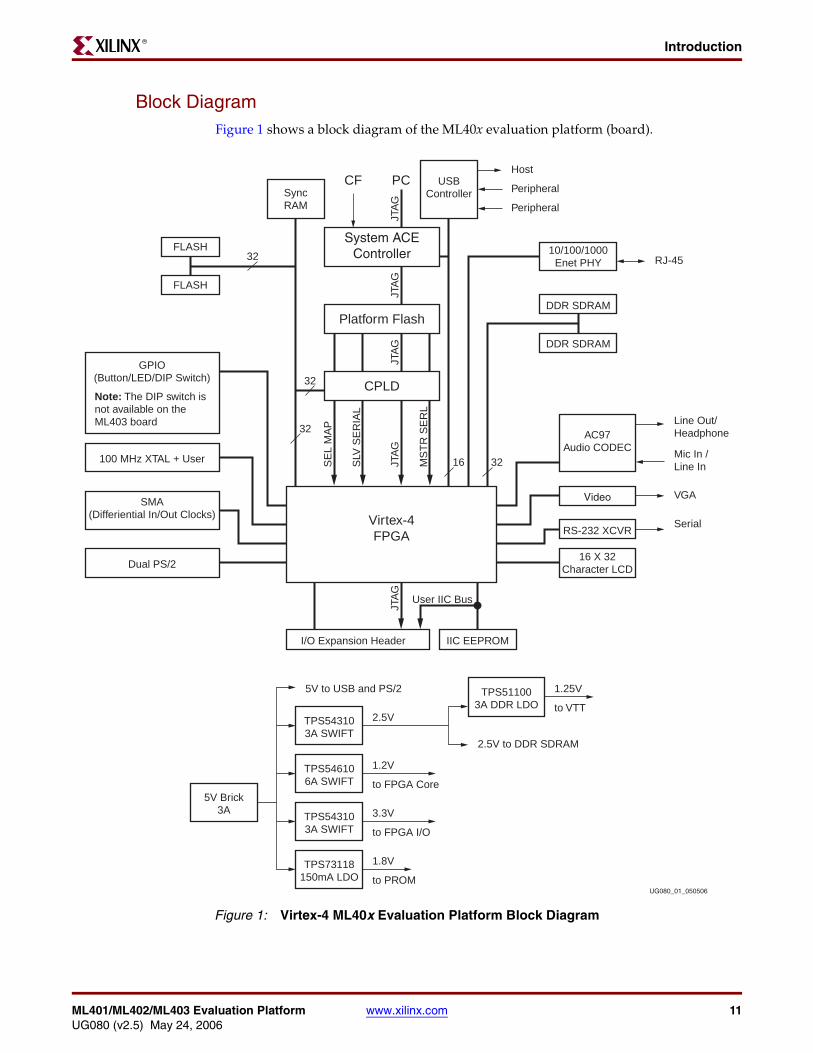
Block DiagramFigure 1 shows a block diagram of the ML40x evaluation platform (board).
Figure 1: Virtex-4 ML40x Evaluation Platform Block Diagram
Virtex-4FPGA
UG080_01_050506
GPIO(Button/LED/DIP Switch)
100 MHz XTAL + User
SMA(Differiential In/Out Clocks)
Dual PS/2
FLASH
FLASH
SyncRAM
CPLD
Platform Flash
System ACEController
SE
L M
AP
SLV
SE
RIA
L
JTA
GJT
AG
JTA
GJT
AG
JTA
G
MS
TR
SE
RL
I/O Expansion Header
USBController
10/100/1000Enet PHY
AC97Audio CODEC
16 X 32Character LCD
CF PC
DDR SDRAM
DDR SDRAM
RS-232 XCVR
Video
IIC EEPROM
RJ-45
Line Out/Headphone
Mic In /Line In
VGA
Serial
Host
Peripheral
Peripheral
32
32
32
3216
TPS543103A SWIFT
TPS546106A SWIFT
TPS511003A DDR LDO
TPS73118150mA LDO
TPS543103A SWIFT
5V Brick3A
1.25V
to VTT
1.2V
2.5V
5V to USB and PS/2
2.5V to DDR SDRAM
to FPGA Core
3.3V
to FPGA I/O
1.8V
to PROM
User IIC Bus
Note: The DIP switch isnot available on theML403 board

12 www.xilinx.com ML401/ML402/ML403 Evaluation PlatformUG080 (v2.5) May 24, 2006
Detailed DescriptionR
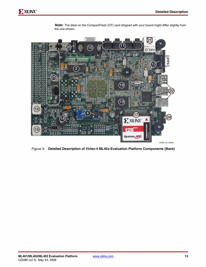
Detailed DescriptionThe ML40x evaluation platform (board) is shown in Figure 2 (front) and Figure 3, page 13 (back). The numbered sections on the pages following the figures contain details on each feature.
Note: The ML402 and ML403 boards might differ slightly from the board shown.
Figure 2: Detailed Description of Virtex-4 ML40x Evaluation Platform Components (Front)
1
13
2
10
20
195
1730
3
23
26 27
32
15
1121
25
7
8
31 33 6 717292879
24
22
12
UG080_02_101504
ML401/ML402/ML403 Evaluation Platform www.xilinx.com 13UG080 (v2.5) May 24, 2006
Detailed DescriptionR
Note: The label on the CompactFlash (CF) card shipped with your board might differ slightly from the one shown.
Figure 3: Detailed Description of Virtex-4 ML40x Evaluation Platform Components (Back)
UG080_03_092004
21
16
16
17
25
144
15 11
18
12
19
2
26
24
22
14 www.xilinx.com ML401/ML402/ML403 Evaluation PlatformUG080 (v2.5) May 24, 2006
Detailed DescriptionR
1. Virtex-4 FPGAA Xilinx Virtex-4 FPGA is installed on the evaluation platform (the board):
♦ ML401: XC4VLX25-FF668-10
♦ ML402: XC4VSX35-FF668-10
♦ ML403: XC4VFX12-FF668-10
Configuration
The board supports configuration in all modes: JTAG, Master Serial, Slave Serial, Master SelectMAP, and Slave SelectMAP modes. See the “Configuration Options,” page 31 section for more information.
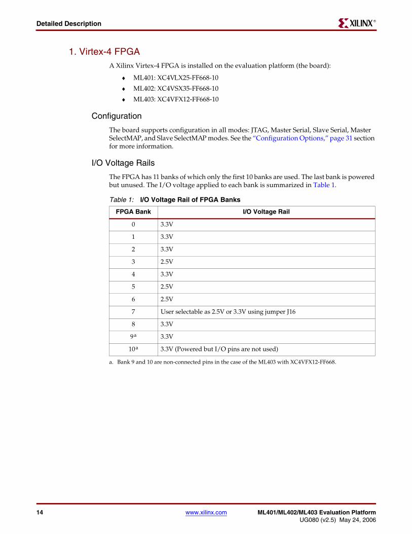
I/O Voltage Rails
The FPGA has 11 banks of which only the first 10 banks are used. The last bank is powered but unused. The I/O voltage applied to each bank is summarized in Table 1.
Table 1: I/O Voltage Rail of FPGA Banks
FPGA Bank I/O Voltage Rail
0 3.3V
1 3.3V
2 3.3V
3 2.5V
4 3.3V
5 2.5V
6 2.5V
7 User selectable as 2.5V or 3.3V using jumper J16
8 3.3V
9a
a. Bank 9 and 10 are non-connected pins in the case of the ML403 with XC4VFX12-FF668.
3.3V
10a 3.3V (Powered but I/O pins are not used)
ML401/ML402/ML403 Evaluation Platform www.xilinx.com 15UG080 (v2.5) May 24, 2006
Detailed DescriptionR
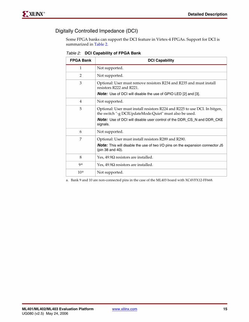
Digitally Controlled Impedance (DCI)
Some FPGA banks can support the DCI feature in Virtex-4 FPGAs. Support for DCI is summarized in Table 2.
Table 2: DCI Capability of FPGA Bank
FPGA Bank DCI Capability
1 Not supported.
2 Not supported.
3 Optional: User must remove resistors R234 and R235 and must install resistors R222 and R221.
Note: Use of DCI will disable the use of GPIO LED [2] and [3].
4 Not supported.
5 Optional: User must install resistors R224 and R225 to use DCI. In bitgen, the switch "-g DCIUpdateMode:Quiet" must also be used.
Note: Use of DCI will disable user control of the DDR_CS_N and DDR_CKE signals.
6 Not supported.
7 Optional: User must install resistors R289 and R290.
Note: This will disable the use of two I/O pins on the expansion connector J5 (pin 38 and 40).
8 Yes, 49.9Ω resistors are installed.
9a
a. Bank 9 and 10 are non-connected pins in the case of the ML403 board with XC4VFX12-FF668.
Yes, 49.9Ω resistors are installed.
10a Not supported.

16 www.xilinx.com ML401/ML402/ML403 Evaluation PlatformUG080 (v2.5) May 24, 2006
Detailed DescriptionR
2. DDR SDRAMThe board contains 64 MB of DDR SDRAM using two Infineon HYB25D256160BT-7 (or compatible) chips (U4 and U5). Each chip is 16 bits wide and together form a 32-bit data bus capable of running up to 266 MHz. All DDR SDRAM signals are terminated through 47Ω resistors to a 1.25V VTT reference voltage. The board is designed for matched length traces across all DDR control and data signals except clocks and the DDR Loop trace (see “DDR Clock Signal” and “DDR Loop Signal”).
The board can support up to 256 MB of total DDR SDRAM memory if larger chips are installed. An extra address pin is present on the board to support up to 1-Gb DDR chips.
DDR Clock Signal
The DDR clock signal is broadcast from the FPGA as a single differential pair that drives both DDR chips. The delay on the clock trace is designed to match the delay of the other DDR control and data signals. The DDR clock is also fed back to the FPGA to allow for clock deskew using Virtex-4 DCMs. The board is designed so that the DDR clock signal reaches the FPGA clock feedback pin at the same time as it arrives at the DDR chips.
DDR Loop Signal
The DDR loop signal is a trace driven and then received back at the FPGA with a delay equal to the sum of the trace delays of the clock and DQS signals. This looped trace can be used in high-speed memory controllers to help compensate for the physical trace delays between the FPGA and DDR chips.
3. Differential Clock Input And Output With SMA ConnectorsHigh-precision clock signals can be input to the FPGA using differential clock signals brought in through 50Ω SMA connectors. This allows an external function generator or other clock source to drive the differential clock inputs that directly feed the global clock input pins of the FPGA. The FPGA can be configured to present a 100Ω termination impedance.
A differential clock output from the FPGA is driven out through a second pair of SMA connectors. This allows the FPGA to drive a precision clock to an external device such as a piece of test equipment. Table 3 summarizes the differential SMA clock pin connections.
Table 3: Differential SMA Clock Connections
Label Clock Name FPGA Pin
J10 SMA_DIFF_CLK_IN_N C12
J7 SMA_DIFF_CLK_IN_P C13
J8 SMA_DIFF_CLK_OUT_N D7
J9 SMA_DIFF_CLK_OUT_P D8
ML401/ML402/ML403 Evaluation Platform www.xilinx.com 17UG080 (v2.5) May 24, 2006
Detailed DescriptionR
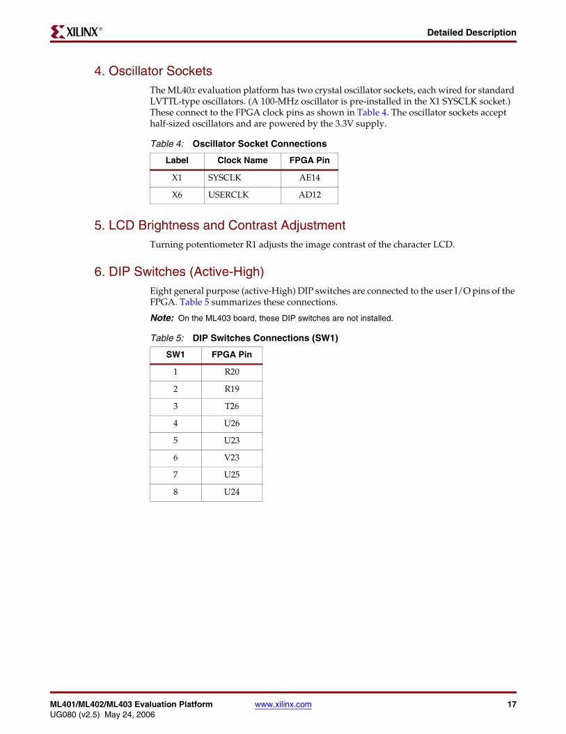
4. Oscillator SocketsThe ML40x evaluation platform has two crystal oscillator sockets, each wired for standard LVTTL-type oscillators. (A 100-MHz oscillator is pre-installed in the X1 SYSCLK socket.) These connect to the FPGA clock pins as shown in Table 4. The oscillator sockets accept half-sized oscillators and are powered by the 3.3V supply.
5. LCD Brightness and Contrast AdjustmentTurning potentiometer R1 adjusts the image contrast of the character LCD.
6. DIP Switches (Active-High)Eight general purpose (active-High) DIP switches are connected to the user I/O pins of the FPGA. Table 5 summarizes these connections.
Note: On the ML403 board, these DIP switches are not installed.
Table 4: Oscillator Socket Connections
Label Clock Name FPGA Pin
X1 SYSCLK AE14
X6 USERCLK AD12
Table 5: DIP Switches Connections (SW1)
SW1 FPGA Pin
1 R20
2 R19
3 T26
4 U26
5 U23
6 V23
7 U25
8 U24
18 www.xilinx.com ML401/ML402/ML403 Evaluation PlatformUG080 (v2.5) May 24, 2006
Detailed DescriptionR
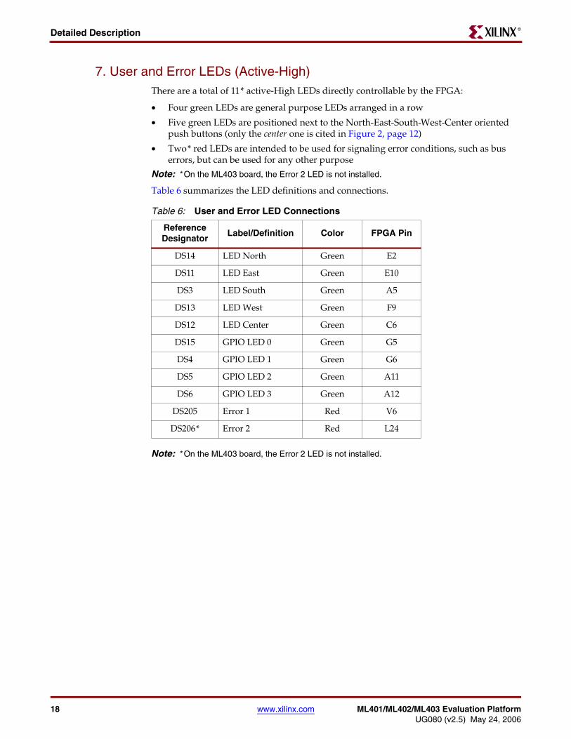
7. User and Error LEDs (Active-High)There are a total of 11* active-High LEDs directly controllable by the FPGA:
• Four green LEDs are general purpose LEDs arranged in a row
• Five green LEDs are positioned next to the North-East-South-West-Center oriented push buttons (only the center one is cited in Figure 2, page 12)
• Two* red LEDs are intended to be used for signaling error conditions, such as bus errors, but can be used for any other purpose
Note: *On the ML403 board, the Error 2 LED is not installed.
Table 6 summarizes the LED definitions and connections.
Note: *On the ML403 board, the Error 2 LED is not installed.
Table 6: User and Error LED Connections
ReferenceDesignator
Label/Definition Color FPGA Pin
DS14 LED North Green E2
DS11 LED East Green E10
DS3 LED South Green A5
DS13 LED West Green F9
DS12 LED Center Green C6
DS15 GPIO LED 0 Green G5
DS4 GPIO LED 1 Green G6
DS5 GPIO LED 2 Green A11
DS6 GPIO LED 3 Green A12
DS205 Error 1 Red V6
DS206* Error 2 Red L24
ML401/ML402/ML403 Evaluation Platform www.xilinx.com 19UG080 (v2.5) May 24, 2006
Detailed DescriptionR
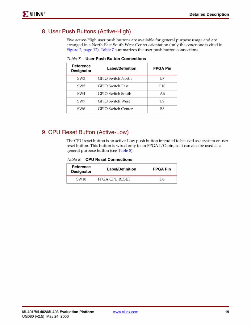
8. User Push Buttons (Active-High)Five active-High user push buttons are available for general purpose usage and are arranged in a North-East-South-West-Center orientation (only the center one is cited in Figure 2, page 12). Table 7 summarizes the user push button connections.
9. CPU Reset Button (Active-Low)The CPU reset button is an active-Low push button intended to be used as a system or user reset button. This button is wired only to an FPGA I/O pin, so it can also be used as a general purpose button (see Table 8).
Table 7: User Push Button Connections
ReferenceDesignator
Label/Definition FPGA Pin
SW3 GPIO Switch North E7
SW5 GPIO Switch East F10
SW4 GPIO Switch South A6
SW7 GPIO Switch West E9
SW6 GPIO Switch Center B6
Table 8: CPU Reset Connections
ReferenceDesignator
Label/Definition FPGA Pin
SW10 FPGA CPU RESET D6
20 www.xilinx.com ML401/ML402/ML403 Evaluation PlatformUG080 (v2.5) May 24, 2006
Detailed DescriptionR
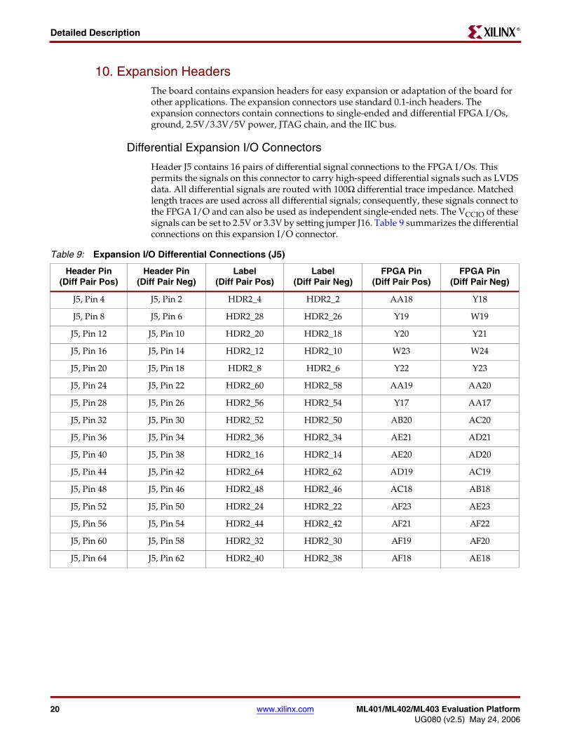
10. Expansion HeadersThe board contains expansion headers for easy expansion or adaptation of the board for other applications. The expansion connectors use standard 0.1-inch headers. The expansion connectors contain connections to single-ended and differential FPGA I/Os, ground, 2.5V/3.3V/5V power, JTAG chain, and the IIC bus.
Differential Expansion I/O Connectors
Header J5 contains 16 pairs of differential signal connections to the FPGA I/Os. This permits the signals on this connector to carry high-speed differential signals such as LVDS data. All differential signals are routed with 100Ω differential trace impedance. Matched length traces are used across all differential signals; consequently, these signals connect to the FPGA I/O and can also be used as independent single-ended nets. The VCCIO of these signals can be set to 2.5V or 3.3V by setting jumper J16. Table 9 summarizes the differential connections on this expansion I/O connector.
Table 9: Expansion I/O Differential Connections (J5)
Header Pin(Diff Pair Pos)
Header Pin(Diff Pair Neg)
Label(Diff Pair Pos)
Label(Diff Pair Neg)
FPGA Pin(Diff Pair Pos)
FPGA Pin(Diff Pair Neg)
J5, Pin 4 J5, Pin 2 HDR2_4 HDR2_2 AA18 Y18
J5, Pin 8 J5, Pin 6 HDR2_28 HDR2_26 Y19 W19
J5, Pin 12 J5, Pin 10 HDR2_20 HDR2_18 Y20 Y21
J5, Pin 16 J5, Pin 14 HDR2_12 HDR2_10 W23 W24
J5, Pin 20 J5, Pin 18 HDR2_8 HDR2_6 Y22 Y23
J5, Pin 24 J5, Pin 22 HDR2_60 HDR2_58 AA19 AA20
J5, Pin 28 J5, Pin 26 HDR2_56 HDR2_54 Y17 AA17
J5, Pin 32 J5, Pin 30 HDR2_52 HDR2_50 AB20 AC20
J5, Pin 36 J5, Pin 34 HDR2_36 HDR2_34 AE21 AD21
J5, Pin 40 J5, Pin 38 HDR2_16 HDR2_14 AE20 AD20
J5, Pin 44 J5, Pin 42 HDR2_64 HDR2_62 AD19 AC19
J5, Pin 48 J5, Pin 46 HDR2_48 HDR2_46 AC18 AB18
J5, Pin 52 J5, Pin 50 HDR2_24 HDR2_22 AF23 AE23
J5, Pin 56 J5, Pin 54 HDR2_44 HDR2_42 AF21 AF22
J5, Pin 60 J5, Pin 58 HDR2_32 HDR2_30 AF19 AF20
J5, Pin 64 J5, Pin 62 HDR2_40 HDR2_38 AF18 AE18
ML401/ML402/ML403 Evaluation Platform www.xilinx.com 21UG080 (v2.5) May 24, 2006
Detailed DescriptionR
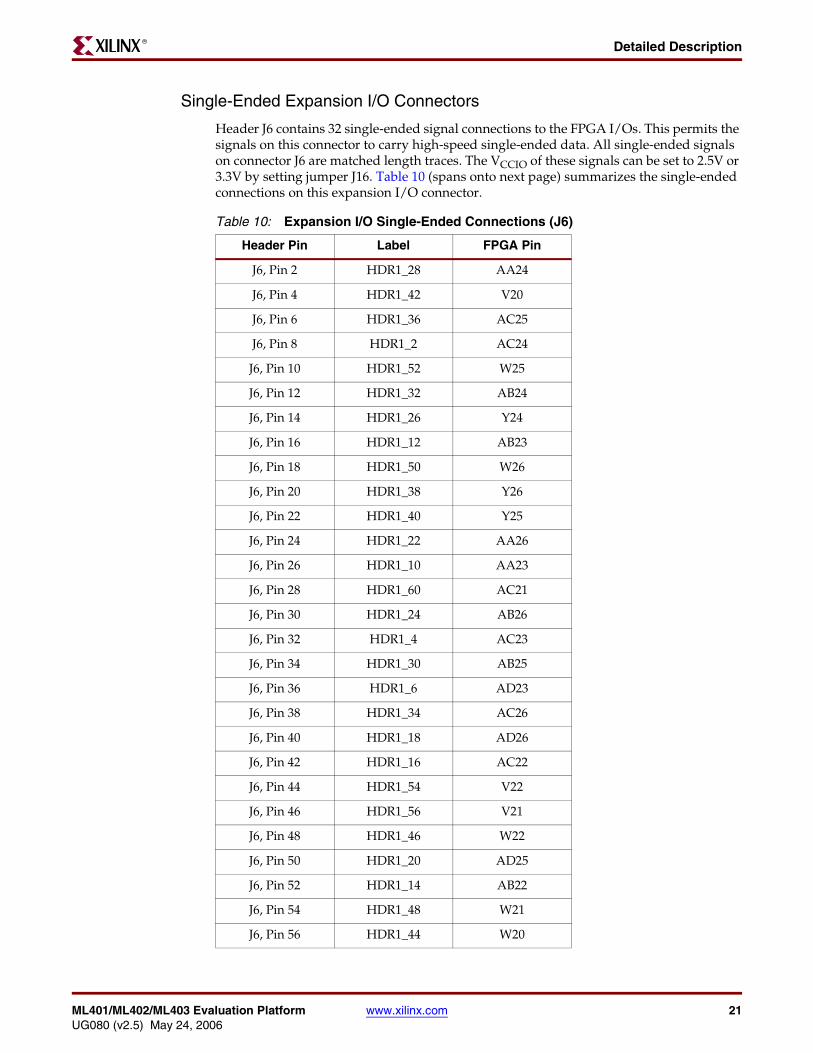
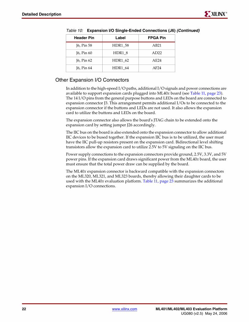
Single-Ended Expansion I/O Connectors
Header J6 contains 32 single-ended signal connections to the FPGA I/Os. This permits the signals on this connector to carry high-speed single-ended data. All single-ended signals on connector J6 are matched length traces. The VCCIO of these signals can be set to 2.5V or 3.3V by setting jumper J16. Table 10 (spans onto next page) summarizes the single-ended connections on this expansion I/O connector.
Table 10: Expansion I/O Single-Ended Connections (J6)
Header Pin Label FPGA Pin
J6, Pin 2 HDR1_28 AA24
J6, Pin 4 HDR1_42 V20
J6, Pin 6 HDR1_36 AC25
J6, Pin 8 HDR1_2 AC24
J6, Pin 10 HDR1_52 W25
J6, Pin 12 HDR1_32 AB24
J6, Pin 14 HDR1_26 Y24
J6, Pin 16 HDR1_12 AB23
J6, Pin 18 HDR1_50 W26
J6, Pin 20 HDR1_38 Y26
J6, Pin 22 HDR1_40 Y25
J6, Pin 24 HDR1_22 AA26
J6, Pin 26 HDR1_10 AA23
J6, Pin 28 HDR1_60 AC21
J6, Pin 30 HDR1_24 AB26
J6, Pin 32 HDR1_4 AC23
J6, Pin 34 HDR1_30 AB25
J6, Pin 36 HDR1_6 AD23
J6, Pin 38 HDR1_34 AC26
J6, Pin 40 HDR1_18 AD26
J6, Pin 42 HDR1_16 AC22
J6, Pin 44 HDR1_54 V22
J6, Pin 46 HDR1_56 V21
J6, Pin 48 HDR1_46 W22
J6, Pin 50 HDR1_20 AD25
J6, Pin 52 HDR1_14 AB22
J6, Pin 54 HDR1_48 W21
J6, Pin 56 HDR1_44 W20
22 www.xilinx.com ML401/ML402/ML403 Evaluation PlatformUG080 (v2.5) May 24, 2006
Detailed DescriptionR
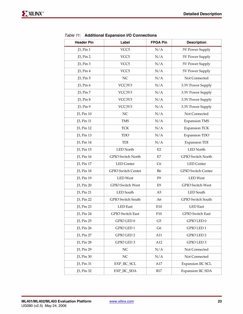
Other Expansion I/O Connectors
In addition to the high-speed I/O paths, additional I/O signals and power connections are available to support expansion cards plugged into ML40x board (see Table 11, page 23). The 14 I/O pins from the general purpose buttons and LEDs on the board are connected to expansion connector J3. This arrangement permits additional I/Os to be connected to the expansion connector if the buttons and LEDs are not used. It also allows the expansion card to utilize the buttons and LEDs on the board.
The expansion connector also allows the board's JTAG chain to be extended onto the expansion card by setting jumper J26 accordingly.
The IIC bus on the board is also extended onto the expansion connector to allow additional IIC devices to be bused together. If the expansion IIC bus is to be utilized, the user must have the IIC pull-up resistors present on the expansion card. Bidirectional level shifting transistors allow the expansion card to utilize 2.5V to 5V signaling on the IIC bus.
Power supply connections to the expansion connectors provide ground, 2.5V, 3.3V, and 5V power pins. If the expansion card draws significant power from the ML40x board, the user must ensure that the total power draw can be supplied by the board.
The ML40x expansion connector is backward compatible with the expansion connectors on the ML320, ML321, and ML323 boards, thereby allowing their daughter cards to be used with the ML40x evaluation platform. Table 11, page 23 summarizes the additional expansion I/O connections.
J6, Pin 58 HDR1_58 AB21
J6, Pin 60 HDR1_8 AD22
J6, Pin 62 HDR1_62 AE24
J6, Pin 64 HDR1_64 AF24
Table 10: Expansion I/O Single-Ended Connections (J6) (Continued)
Header Pin Label FPGA Pin
ML401/ML402/ML403 Evaluation Platform www.xilinx.com 23UG080 (v2.5) May 24, 2006
Detailed DescriptionR
Table 11: Additional Expansion I/O Connections
Header Pin Label FPGA Pin Description
J3, Pin 1 VCC5 N/A 5V Power Supply
J3, Pin 2 VCC5 N/A 5V Power Supply
J3, Pin 3 VCC5 N/A 5V Power Supply
J3, Pin 4 VCC5 N/A 5V Power Supply
J3, Pin 5 NC N/A Not Connected
J3, Pin 6 VCC3V3 N/A 3.3V Power Supply
J3, Pin 7 VCC3V3 N/A 3.3V Power Supply
J3, Pin 8 VCC3V3 N/A 3.3V Power Supply
J3, Pin 9 VCC3V3 N/A 3.3V Power Supply
J3, Pin 10 NC N/A Not Connected
J3, Pin 11 TMS N/A Expansion TMS
J3, Pin 12 TCK N/A Expansion TCK
J3, Pin 13 TDO N/A Expansion TDO
J3, Pin 14 TDI N/A Expansion TDI
J3, Pin 15 LED North E2 LED North
J3, Pin 16 GPIO Switch North E7 GPIO Switch North
J3, Pin 17 LED Center C6 LED Center
J3, Pin 18 GPIO Switch Center B6 GPIO Switch Center
J3, Pin 19 LED West F9 LED West
J3, Pin 20 GPIO Switch West E9 GPIO Switch West
J3, Pin 21 LED South A5 LED South
J3, Pin 22 GPIO Switch South A6 GPIO Switch South
J3, Pin 23 LED East E10 LED East
J3, Pin 24 GPIO Switch East F10 GPIO Switch East
J3, Pin 25 GPIO LED 0 G5 GPIO LED 0
J3, Pin 26 GPIO LED 1 G6 GPIO LED 1
J3, Pin 27 GPIO LED 2 A11 GPIO LED 2
J3, Pin 28 GPIO LED 3 A12 GPIO LED 3
J3, Pin 29 NC N/A Not Connected
J3, Pin 30 NC N/A Not Connected
J3, Pin 31 EXP_IIC_SCL A17 Expansion IIC SCL
J3, Pin 32 EXP_IIC_SDA B17 Expansion IIC SDA
24 www.xilinx.com ML401/ML402/ML403 Evaluation PlatformUG080 (v2.5) May 24, 2006
Detailed DescriptionR
11. Stereo AC97 Audio CodecThe ML40x board has an AC97 audio codec (U14) to permit audio processing. The National Semiconductor LM4550 Audio Codec supports stereo 16-bit audio with up to 48-kHz sampling. The sampling rate for record and playback can be different.
Note: The reset for the AC97 codec is shared with the reset signal for the flash memory chips and is designed to be asserted at power-on or upon system reset.
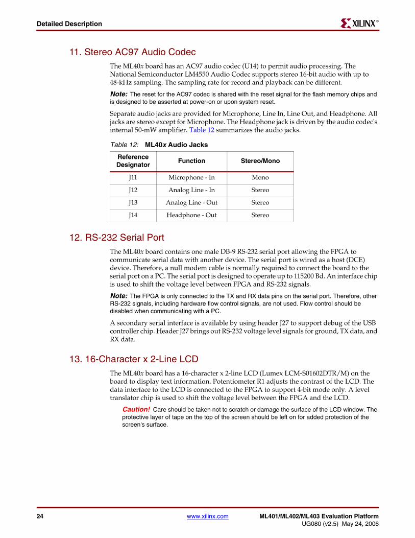
Separate audio jacks are provided for Microphone, Line In, Line Out, and Headphone. All jacks are stereo except for Microphone. The Headphone jack is driven by the audio codec's internal 50-mW amplifier. Table 12 summarizes the audio jacks.
12. RS-232 Serial PortThe ML40x board contains one male DB-9 RS-232 serial port allowing the FPGA to communicate serial data with another device. The serial port is wired as a host (DCE) device. Therefore, a null modem cable is normally required to connect the board to the serial port on a PC. The serial port is designed to operate up to 115200 Bd. An interface chip is used to shift the voltage level between FPGA and RS-232 signals.
Note: The FPGA is only connected to the TX and RX data pins on the serial port. Therefore, other RS-232 signals, including hardware flow control signals, are not used. Flow control should be disabled when communicating with a PC.
A secondary serial interface is available by using header J27 to support debug of the USB controller chip. Header J27 brings out RS-232 voltage level signals for ground, TX data, and RX data.
13. 16-Character x 2-Line LCDThe ML40x board has a 16-character x 2-line LCD (Lumex LCM-S01602DTR/M) on the board to display text information. Potentiometer R1 adjusts the contrast of the LCD. The data interface to the LCD is connected to the FPGA to support 4-bit mode only. A level translator chip is used to shift the voltage level between the FPGA and the LCD.
Caution! Care should be taken not to scratch or damage the surface of the LCD window. The protective layer of tape on the top of the screen should be left on for added protection of the screen's surface.
Table 12: ML40x Audio Jacks
Reference Designator
Function Stereo/Mono
J11 Microphone - In Mono
J12 Analog Line - In Stereo
J13 Analog Line - Out Stereo
J14 Headphone - Out Stereo
ML401/ML402/ML403 Evaluation Platform www.xilinx.com 25UG080 (v2.5) May 24, 2006
Detailed DescriptionR
14. IIC Bus with 4-Kb EEPROMAn IIC EEPROM (Microchip Technology 24LC04B-I/ST) is provided on the ML40x board to store non-volatile data such as an Ethernet MAC address. The EEPROM write protect is tied off on the board to disable its hardware write protect. The IIC bus uses 2.5V signaling and can operate at up to 400 kHz. IIC bus pull-up resistors are provided on the board.
The IIC bus is extended to the expansion connector so that the user may add additional IIC devices and share the IIC controller in the FPGA. If the expansion IIC bus is to be utilized, the user must have additional IIC pull-up resistors present on the expansion card. Bidirectional level shifting transistors allow the expansion card to utilize 2.5V to 5V signaling on IIC.
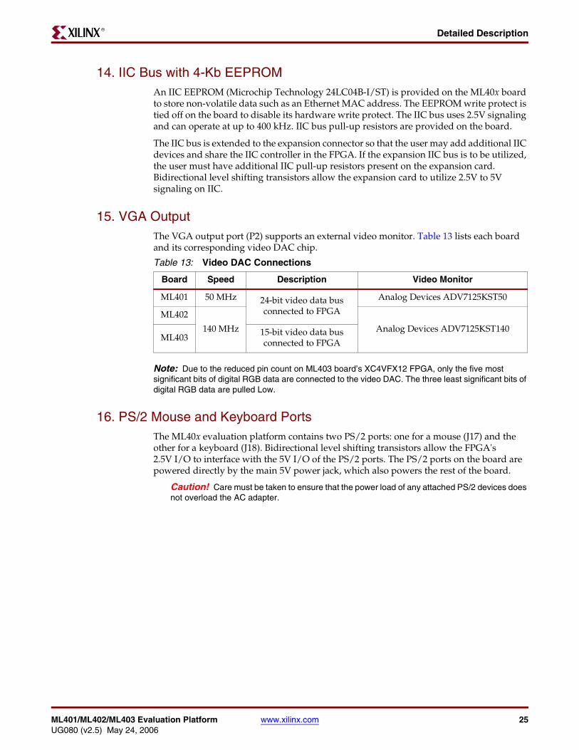
15. VGA OutputThe VGA output port (P2) supports an external video monitor. Table 13 lists each board and its corresponding video DAC chip.
Note: Due to the reduced pin count on ML403 board’s XC4VFX12 FPGA, only the five most significant bits of digital RGB data are connected to the video DAC. The three least significant bits of digital RGB data are pulled Low.
16. PS/2 Mouse and Keyboard PortsThe ML40x evaluation platform contains two PS/2 ports: one for a mouse (J17) and the other for a keyboard (J18). Bidirectional level shifting transistors allow the FPGA's 2.5V I/O to interface with the 5V I/O of the PS/2 ports. The PS/2 ports on the board are powered directly by the main 5V power jack, which also powers the rest of the board.
Caution! Care must be taken to ensure that the power load of any attached PS/2 devices does not overload the AC adapter.
Table 13: Video DAC Connections
Board Speed Description Video Monitor
ML401 50 MHz 24-bit video data bus connected to FPGA
Analog Devices ADV7125KST50
ML402
140 MHz Analog Devices ADV7125KST140ML403
15-bit video data bus connected to FPGA
26 www.xilinx.com ML401/ML402/ML403 Evaluation PlatformUG080 (v2.5) May 24, 2006
Detailed DescriptionR
17. System ACE and CompactFlash ConnectorThe Xilinx System ACE CompactFlash (CF) configuration controller allows a Type I or Type II CompactFlash card to program the FPGA through the JTAG port. Both hardware and software data can be downloaded through the JTAG port. The System ACE controller supports up to eight configuration images on a single CompactFlash card. The configuration address switches allow the user to choose which of the eight configuration images to use.
System ACE error and status LEDs indicate the operational state of the System ACE controller:
• A blinking red error LED indicates that no CompactFlash card is present
• A solid red error LED indicates an error condition during configuration
• A blinking green status LED indicates a configuration operation is ongoing
• A solid green status LED indicates a successful download
Every time a CompactFlash card is inserted into the System ACE socket, a configuration operation is initiated. Pressing the System ACE reset button re-programs the FPGA.
The board also features a System ACE failsafe mode. In this mode, if the System ACE controller detects a failed configuration attempt, it automatically reboots back to a predefined configuration image. The failsafe mode is enabled by inserting two jumpers across J29 and J30 (in horizontal or vertical orientation).
Caution! Use caution when inserting a CompactFlash card with exposed metallic surfaces. Improper insertion can cause a short with the traces or components on the board.
The System ACE MPU port is connected to the FPGA. This connection allows the FPGA to use the System ACE controller to reconfigure the system or access the CompactFlash card as a generic FAT file system. The data bus for the System ACE MPU port is shared with the USB controller.
For configuration through the System ACE controller, the configuration selector switch (SW12) must be set to the SYS ACE position.
18. ZBT Synchronous SRAMThe ZBT synchronous SRAM (Cypress CY7C1354B or compatible) provides high-speed, low-latency external memory to the FPGA. The memory is organized as 256K x 36 bits. This organization provides for a 32-bit data bus with support for four parity bits. On ML403, the parity bits are not accessible.
Note: The SRAM and FLASH memory share the same data bus.

ML401/ML402/ML403 Evaluation Platform www.xilinx.com 27UG080 (v2.5) May 24, 2006
Detailed DescriptionR
19. Linear Flash ChipsTwo 32-Mb linear flash devices (Micron MT28F320J3RG-11 ET) are installed on the board for a total of 8 MB of flash memory. These flash memory chips are Intel StrataFlash compatible. This memory provides non-volatile storage of data, software, or bitstreams. Each flash chip is 16 bits wide and together forms a 32-bit data bus that is shared with SRAM. In conjunction with a CPLD, the flash memory can also be used to program the FPGA.
Note: The reset for the AC97 Codec is shared with the reset signal for the flash memory chips and is designed to be asserted at power-on or upon system reset.
20. Xilinx XC95144XL CPLDA Xilinx XC95144XL CPLD is connected to the flash memory and the FPGA configuration signals. This CPLD connection supports applications where flash memory programs the FPGA. The CPLD is programmed from the main JTAG chain of the board. The CPLD is wired so that it can support master or slave configuration in serial or parallel (SelectMAP) modes. For FPGA configuration via the CPLD and flash, the configuration selector switch (SW12) must be set to the CPLD Flash position. See the “Configuration Options,” page 31 section for more information.
21. 10/100/1000 Tri-Speed Ethernet PHYThe ML40x evaluation platform contains a Marvell Alaska PHY device (88E1111) operating at 10/100/1000 Mb/s. The board supports MII, GMII, and RGMII interface modes with the FPGA. The PHY is connected to a Halo HFJ11-1G01E RJ-45 connector with built-in magnetics. A 25-MHz crystal supplies the clock signal to the PHY. The PHY is configured to default at power-on or reset to the following settings (See Table 14). These settings may be overwritten via software.
Table 14: Board Connections for PHY Configuration Pins
Config PinConnection on
BoardBit[2] Definition and
ValueBit[1] Definition and
ValueBit[0] Definition and Value
CONFIG0 Ground PHYADR[2] = 0 PHYADR[1] = 0 PHYADR[0] = 0
CONFIG1 Ground ENA_PAUSE = 0 PHYADR[4] = 0 PHYADR[3] = 0
CONFIG2 VCC 2.5V ANEG[3] = 1 ANEG[2] = 1 ANEG[1] = 1
CONFIG3 VCC 2.5V ANEG[0] = 1 ENA_XC = 1 DIS_125 = 1
CONFIG4 VCC 2.5V HWCFG_MODE[2] = 1 HWCFG_MODE[1] = 1 HWCFG_MODE[0] = 1
CONFIG5 VCC 2.5V DIS_FC = 1 DIS_SLEEP = 1 HWCFG_MODE[3] = 1
CONFIG6 LED_RX SEL_BDT = 0 INT_POL = 1 75/50Ω = 0
28 www.xilinx.com ML401/ML402/ML403 Evaluation PlatformUG080 (v2.5) May 24, 2006
Detailed DescriptionR
22. USB Controller with Host and Peripheral PortsA Cypress CY7C67300 embedded USB host controller provides USB connectivity for the board. The USB controller supports host and peripheral modes of operation. The USB controller has two serial interface engines (SIE) that can be used independently. SIE1 is connected to the USB Host 1 connector (J19) and the USB Peripheral 1 connector (J2). SIE2 is connected only to the USB Peripheral 2 connector.
Note: When using SIE1, the port can only be configured at boot-up to use either the host or peripheral connector, but not both at the same time.
The USB controller has an internal microprocessor to assist in processing USB commands. The firmware for this processor can be stored in its own dedicated IIC EEPROM (U17) or can be downloaded from a host computer via a peripheral connector. The USB controller's serial port is connected to J27 through an RS-232 transceiver to assist with debug.
23. Xilinx XCF32P Platform Flash Configuration Storage DeviceXilinx XCF32P Platform Flash configuration storage device offers a convenient and easy-to-use configuration solution for the FPGA. The Platform Flash memory holds up to four separate configuration images (two images on the ML402 board) that can be accessed through the configuration address switches. To use the Platform Flash memory to configure the FPGA, the configuration selector switch (SW12) must be set to the Plat Flash position.
The Platform Flash memory can program the FPGA by using the master or slave configuration in serial or parallel (SelectMap) modes. The Platform Flash memory is programmed using Xilinx iMPACT software through the board’s JTAG chain. See the “Configuration Options,” page 31 section for more information.
24. JTAG Configuration PortThe JTAG configuration port for the board (J20) allows for device programming and FPGA debug. The JTAG port supports the Xilinx Parallel Cable III or Parallel Cable IV products. Third-party configuration products might also be available. The JTAG chain can also be extended to an expansion board by setting jumper J26 accordingly. See the “Configuration Options,” page 31 section for more information.

ML401/ML402/ML403 Evaluation Platform www.xilinx.com 29UG080 (v2.5) May 24, 2006
Detailed DescriptionR
25. Onboard Power SuppliesPower supply circuitry on the board generates 1.2V, 1.25V, 1.8V, 2.5V, and 3.3V voltages to power the components on the board. The 1.2V, 2.5V, and 3.3V supplies are driven by switching power regulators. When these three switching regulators report they are running at their nominal voltages, the PWR Good LED is turned on.
The diagram in Figure 4 shows the power supply architecture and maximum current handling on each supply. The typical operating currents are significantly below the maximum capable. The ML40x board is normally shipped with a 15W power supply which should be sufficient for most applications.
26. AC Adapter and Input Power Switch/JackThe ML40x board ships with a 15W (5V @ 3A) AC adapter. The power connector is a 2.1 mm x 5.5 mm barrel type plug (center positive). For applications requiring additional power, such as the use of expansion cards drawing significant power, a larger AC adapter might be required. If a different AC adapter is used, its load regulation should be less than 10% or better than ±10%. The power switch turns the board on and off by controlling the supply of 5V to the board.
27. Power Indicator LEDThe PWR Good LED lights when the 1.2V, 2.5V, and 3.3V power supplies are all at their nominal operating conditions. If the PWR Good LED is off, blinking, or glowing lightly, this indicates a fault condition, such as a short or overload condition, might exist.
28. INIT LEDThe INIT LED lights upon power-up to indicate that the FPGA has successfully powered up and completed its internal power-on process.
Figure 4: Power Supply Diagram
TPS543103A SWIFT
TPS546106A SWIFT
TPS511003A DDR LDO
TPS73118150mA LDO
TPS543103A SWIFT
5V Brick3A
1.25V
to VTT
1.2V
2.5V
5V to USB and PS/2
2.5V to DDR SDRAM
to FPGA Core
3.3V
to FPGA I/O
1.8V
to PROMUG080_04_022305
30 www.xilinx.com ML401/ML402/ML403 Evaluation PlatformUG080 (v2.5) May 24, 2006
Detailed DescriptionR
29. DONE LEDThe DONE LED indicates the status of the DONE pin on the FPGA. It should be lighted when the FPGA is successfully configured.
30. Program SwitchThis switch grounds the FPGA's Prog pin when pressed. This action clears the FPGA.
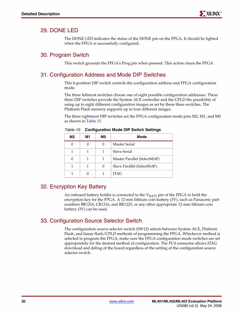
31. Configuration Address and Mode DIP SwitchesThis 6-position DIP switch controls the configuration address and FPGA configuration mode.
The three leftmost switches choose one of eight possible configuration addresses. These three DIP switches provide the System ACE controller and the CPLD the possibility of using up to eight different configuration images as set by these three switches. The Platform Flash memory supports up to four different images.
The three rightmost DIP switches set the FPGA configuration mode pins M2, M1, and M0 as shown in Table 15.
32. Encryption Key Battery An onboard battery holder is connected to the VBATT pin of the FPGA to hold the encryption key for the FPGA. A 12-mm lithium coin battery (3V), such as Panasonic part numbers BR1216, CR1216, and BR1225, or any other appropriate 12-mm lithium coin battery (3V) can be used.
33. Configuration Source Selector Switch The configuration source selector switch (SW12) selects between System ACE, Platform Flash, and linear flash/CPLD methods of programming the FPGA. Whichever method is selected to program the FPGA, make sure the FPGA configuration mode switches are set appropriately for the desired method of configuration. The PC4 connector allows JTAG download and debug of the board regardless of the setting of the configuration source selector switch.
Table 15: Configuration Mode DIP Switch Settings
M2 M1 M0 Mode
0 0 0 Master Serial
1 1 1 Slave Serial
0 1 1 Master Parallel (SelectMAP)
1 1 0 Slave Parallel (SelectMAP)
1 0 1 JTAG
ML401/ML402/ML403 Evaluation Platform www.xilinx.com 31UG080 (v2.5) May 24, 2006
Configuration OptionsR
Configuration OptionsThe FPGA on the ML40x evaluation platform can be configured by four major devices:
• Parallel Cable IV cable (JTAG)
• System ACE controller (JTAG)
• Platform Flash memory
• Linear flash + CPLD
The following section provides an overview of the possible ways the board can be configured.
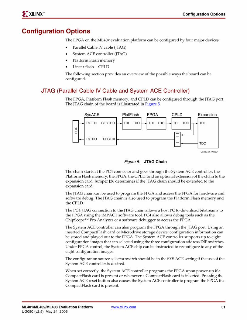
JTAG (Parallel Cable IV Cable and System ACE Controller)The FPGA, Platform Flash memory, and CPLD can be configured through the JTAG port. The JTAG chain of the board is illustrated in Figure 5.
The chain starts at the PC4 connector and goes through the System ACE controller, the Platform Flash memory, the FPGA, the CPLD, and an optional extension of the chain to the expansion card. Jumper J26 determines if the JTAG chain should be extended to the expansion card.
The JTAG chain can be used to program the FPGA and access the FPGA for hardware and software debug. The JTAG chain is also used to program the Platform Flash memory and the CPLD.
The PC4 JTAG connection to the JTAG chain allows a host PC to download bitstreams to the FPGA using the iMPACT software tool. PC4 also allows debug tools such as the ChipScope™ Pro Analyzer or a software debugger to access the FPGA.
The System ACE controller can also program the FPGA through the JTAG port. Using an inserted CompactFlash card or Microdrive storage device, configuration information can be stored and played out to the FPGA. The System ACE controller supports up to eight configuration images that can selected using the three configuration address DIP switches. Under FPGA control, the System ACE chip can be instructed to reconfigure to any of the eight configuration images.
The configuration source selector switch should be in the SYS ACE setting if the use of the System ACE controller is desired.
When set correctly, the System ACE controller programs the FPGA upon power-up if a CompactFlash card is present or whenever a CompactFlash card is inserted. Pressing the System ACE reset button also causes the System ACE controller to program the FPGA if a CompactFlash card is present.
Figure 5: JTAG Chain
UG080_05_090804
PlatFlash FPGASysACE
TSTTDI TDI
TSTDO
CFGTDO TDO
CFGTDI
PC
4
TDI TDO
CPLD
TDI TDO
Expansion
TDI
TDO
32 www.xilinx.com ML401/ML402/ML403 Evaluation PlatformUG080 (v2.5) May 24, 2006
Configuration OptionsR
Platform Flash MemoryThe Platform Flash memory can also be used to program the FPGA. The Platform Flash memory can hold up to four configuration images, which are selectable by the two least significant bits of the configuration address DIP switches.
Note: ML402 Platform Flash memory can hold two configuration images, which are selectable by the least significant bit of the configuration address DIP switches.
The board is wired so the Platform Flash memory can download bitstreams in Master Serial, Slave Serial, Master SelectMAP (parallel), or Slave SelectMAP (parallel) modes. Using the iMPACT tool to program the Platform Flash memory, the user has the option to select which of the four modes to use for programming the FPGA. The configuration mode DIP switches on the board must be set to match the programming method being used by the Platform Flash memory.
The configuration source selector switch should be in the Plat Flash setting if the use of Platform Flash memory is desired.
When set correctly, the Platform Flash memory programs the FPGA upon power-up or whenever the Prog button is pressed.
Linear Flash + CPLDData stored in the linear flash can be read by the CPLD and used to program the FPGA. Depending on the logic design in the CPLD, up to eight configuration images can theoretically be supported.
Note: Note: ML402 linear flash can hold up to four configuration images.
The board is wired so the CPLD can download bitstreams via Master Serial, Slave Serial, Master SelectMAP (parallel), or Slave SelectMAP (parallel) modes. The configuration mode DIP switches on the board must be set to match the programming method being used by the CPLD.
The configuration source selector switch should be in the CPLD Flash setting if the use of CPLD + Platform Flash is desired.
When set correctly, the CPLD programs the FPGA upon power-up or whenever the Prog button is pressed.
Related Documents