Sensors and Actuators B 163 (2012) 159–164 Contents lists available at SciVerse ScienceDirect Sensors and Actuators B: Chemical journa l h o mepage: www.elsevier.com/locate/snb Enhancing hydrogen sensitivity of porous GaN by using simple and low cost photoelectrochemical etching techniques K. Al-Heuseen a,∗ , M.R. Hashim b a Al-Balqa’ Applied University, Ajloun University College, Jordan b Nano-Optoelectronics Research Laboratory, School of Physics, Universiti Sains Malaysia, 11800 Penang, Malaysia a r t i c l e i n f o Article history: Received 16 October 2011 Received in revised form 7 January 2012 Accepted 10 January 2012 Available online 18 January 2012 Keywords: Porous GaN Hydrogen sensor Schottky diodes Sensitivity a b s t r a c t This paper reports the studies of Pd Schottky contact on porous n-GaN for hydrogen gas sensor. A sim- ple conventional and low cost photoelectrochemical etching method was used to produce porous GaN with high uniformity. Hydrogen sensor was subsequently fabricated by depositing Pd Schottky contacts onto the porous GaN sample. For comparative study, a standard hydrogen sensor was also prepared by depositing Pd Schottky contacts on the as-grown sample. The Pd/porous GaN sensor exhibited a signif- icant change of current upon exposure to different flow rates of 2% H 2 in N 2 gas as compared to the standard Pd/GaN sensor. The response increased exponentially with hydrogen flow rate for both sensors, but Pd/porous GaN is more sensitive to hydrogen than that of the as-grown GaN. The values of ideality factor (n), barrier height (ϕ B ) and series resistance (R s ) were calculated in both sensors. Barrier heights and series resistance decreased with H 2 flow rate while ideality factor increased. © 2012 Elsevier B.V. All rights reserved. 1. Introduction During the last decades, porous semiconductors have been widely studied because of their physical properties relative to those of bulk crystals. The high surface area, band gap shift, and effi- cient luminescence have made the use of porous semiconductor as promising material for a wide range of applications; from opto- electronics to chemical and biochemical sensors. Porous layers in semiconductor are very attractive from a sensor point of view because of a unique combination of crystalline structure; a large internal surface area of up to (200–500 m 2 cm −3 ) and high activity in surface chemical reactions. Several investigations showed that electrical and optical characteristics of porous semiconductors may change considerably upon adsorption of molecules to their surfaces and by filling the pores [1–3]. This means that surface adsorption and capillary condensation effects in porous semiconductor layers can be used for the development of effective sensor systems [4,5]. The advantages of using porous semiconductor layers in sensors applications in comparison with other porous materials such as ceramics or nano-polycrystalline films of metal oxides are as fol- lows: (1) it is basically a crystalline material and thus, in principle, is perfectly compatible with common microelectronic processes devices. (2) It can be electrochemically fabricated by very simple ∗ Corresponding author. Fax: +60 4 6579150. E-mail addresses: [email protected] (K. Al-Heuseen), [email protected] (M.R. Hashim). and cheap equipment. (3) It can be produced in a large variety of morphologies, all exhibiting large values of surface-to-volume ratio [6]. Wide band gap semiconductors such as GaN are an ideal mate- rial for sensing application, particularly in harsh environments. Recently, the development of chemical sensors has received con- siderable attention due to the great demand for industrial and environmental applications. Detection of hydrogen gas is one of the potential industrial applications, because hydrogen is one of the most important applied gases, and there are significant recent interests in the development of hydrogen gas sensors for use in fuel cells as an energy source to replace petroleum. Hydrogen gas sensors play a critical role, particularly for fuel leak detection in spacecraft, automobiles, and aircraft, fire detectors, and diagnosis of exhaust and emissions from industrial processes since hydrogen is a hazardous, odorless, and highly flammable gas [7–10]. From the literature, there are a few reports on using porous GaN [11,12] as a gas sensor, and the mechanism involved in gas sens- ing using these materials still need more investigation. Schottky barrier-type gas sensors are typical sensors fabricated based on standard semiconductors [13,14]. Typical Schottky barriers were formed by deposition of Pt [11,15], Pd [12,16,17], Au [18,19] and Al [20]. In this work, a cost effective photoelectrochemical etching tech- nique was used to produce porous GaN nanostructures. These GaN nanostructures were used to fabricate Pd Schottky contact gas sensor for hydrogen detection at room temperature. For com- parative study, a standard hydrogen sensor was also prepared by 0925-4005/$ – see front matter © 2012 Elsevier B.V. All rights reserved. doi:10.1016/j.snb.2012.01.029

Welcome message from author
This document is posted to help you gain knowledge. Please leave a comment to let me know what you think about it! Share it to your friends and learn new things together.
Transcript
Ep
Ka
b
a
ARRAA
KPHSS
1
wocaesbiiecaacTaclid
(
0d
Sensors and Actuators B 163 (2012) 159– 164
Contents lists available at SciVerse ScienceDirect
Sensors and Actuators B: Chemical
journa l h o mepage: www.elsev ier .com/ locate /snb
nhancing hydrogen sensitivity of porous GaN by using simple and low costhotoelectrochemical etching techniques
. Al-Heuseena,∗, M.R. Hashimb
Al-Balqa’ Applied University, Ajloun University College, JordanNano-Optoelectronics Research Laboratory, School of Physics, Universiti Sains Malaysia, 11800 Penang, Malaysia
r t i c l e i n f o
rticle history:eceived 16 October 2011eceived in revised form 7 January 2012ccepted 10 January 2012vailable online 18 January 2012
a b s t r a c t
This paper reports the studies of Pd Schottky contact on porous n-GaN for hydrogen gas sensor. A sim-ple conventional and low cost photoelectrochemical etching method was used to produce porous GaNwith high uniformity. Hydrogen sensor was subsequently fabricated by depositing Pd Schottky contactsonto the porous GaN sample. For comparative study, a standard hydrogen sensor was also prepared by
eywords:orous GaNydrogen sensorchottky diodesensitivity
depositing Pd Schottky contacts on the as-grown sample. The Pd/porous GaN sensor exhibited a signif-icant change of current upon exposure to different flow rates of 2% H2 in N2 gas as compared to thestandard Pd/GaN sensor. The response increased exponentially with hydrogen flow rate for both sensors,but Pd/porous GaN is more sensitive to hydrogen than that of the as-grown GaN. The values of idealityfactor (n), barrier height (ϕB) and series resistance (Rs) were calculated in both sensors. Barrier heightsand series resistance decreased with H2 flow rate while ideality factor increased.
. Introduction
During the last decades, porous semiconductors have beenidely studied because of their physical properties relative to those
f bulk crystals. The high surface area, band gap shift, and effi-ient luminescence have made the use of porous semiconductors promising material for a wide range of applications; from opto-lectronics to chemical and biochemical sensors. Porous layers inemiconductor are very attractive from a sensor point of viewecause of a unique combination of crystalline structure; a large
nternal surface area of up to (200–500 m2 cm−3) and high activityn surface chemical reactions. Several investigations showed thatlectrical and optical characteristics of porous semiconductors mayhange considerably upon adsorption of molecules to their surfacesnd by filling the pores [1–3]. This means that surface adsorptionnd capillary condensation effects in porous semiconductor layersan be used for the development of effective sensor systems [4,5].he advantages of using porous semiconductor layers in sensorspplications in comparison with other porous materials such aseramics or nano-polycrystalline films of metal oxides are as fol-
ows: (1) it is basically a crystalline material and thus, in principle,s perfectly compatible with common microelectronic processesevices. (2) It can be electrochemically fabricated by very simple∗ Corresponding author. Fax: +60 4 6579150.E-mail addresses: [email protected] (K. Al-Heuseen), [email protected]
M.R. Hashim).
925-4005/$ – see front matter © 2012 Elsevier B.V. All rights reserved.oi:10.1016/j.snb.2012.01.029
© 2012 Elsevier B.V. All rights reserved.
and cheap equipment. (3) It can be produced in a large variety ofmorphologies, all exhibiting large values of surface-to-volume ratio[6].
Wide band gap semiconductors such as GaN are an ideal mate-rial for sensing application, particularly in harsh environments.Recently, the development of chemical sensors has received con-siderable attention due to the great demand for industrial andenvironmental applications. Detection of hydrogen gas is one ofthe potential industrial applications, because hydrogen is one ofthe most important applied gases, and there are significant recentinterests in the development of hydrogen gas sensors for use infuel cells as an energy source to replace petroleum. Hydrogen gassensors play a critical role, particularly for fuel leak detection inspacecraft, automobiles, and aircraft, fire detectors, and diagnosisof exhaust and emissions from industrial processes since hydrogenis a hazardous, odorless, and highly flammable gas [7–10].
From the literature, there are a few reports on using porous GaN[11,12] as a gas sensor, and the mechanism involved in gas sens-ing using these materials still need more investigation. Schottkybarrier-type gas sensors are typical sensors fabricated based onstandard semiconductors [13,14]. Typical Schottky barriers wereformed by deposition of Pt [11,15], Pd [12,16,17], Au [18,19] and Al[20].
In this work, a cost effective photoelectrochemical etching tech-
nique was used to produce porous GaN nanostructures. TheseGaN nanostructures were used to fabricate Pd Schottky contactgas sensor for hydrogen detection at room temperature. For com-parative study, a standard hydrogen sensor was also prepared by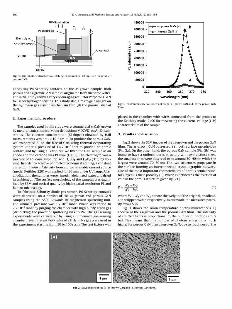
160 K. Al-Heuseen, M.R. Hashim / Sensors and Actuators B 163 (2012) 159– 164
Fp
dpTttG
2
bsmwscamuc(aiiR
wsT2(ect
ig. 1. The photoelectrochemical etching experimental set up used to produceorous GaN.
epositing Pd Schottky contacts on the as-grown sample. Bothorous and as-grown GaN samples originated from the same wafer.he initial study shows a very encouraging result for Pd/porous GaNo use for hydrogen sensing. This study also, aims to gain insight onhe hydrogen gas sensor mechanism through the porous layer ofaN.
. Experimental procedure
The samples used in this study were commercial n-GaN growny metalorganic chemical vapor deposition (MOCVD) on Al2O3 sub-trates. The electron concentration (Si doped) obtained by Halleasurements was n = 1 × 1017 cm−3. To produce the porous GaN,e evaporated Al on the face of GaN using thermal evaporating
ystem under a pressure of 3.4 × 10⁻⁵ Torr to provide an ohmicontact, and by using a Teflon cell we fixed the GaN sample as annode and the cathode was Pt wire (Fig. 1). The electrolyte was aixture of aqueous sulphuric acid H2SO4 and H2O2 (3:1) by vol-
me. In order to achieve photoelectrochemical etching, a constanturrent of 5 mA/cm2 density from a programmable current sourcemodel Keithley 220) was applied for 30 min under UV lamp. Afternodization, the samples were rinsed in deionized water and driedn ambient air. The surface morphology of the samples was exam-ned by SEM and optical quality by high-spatial resolution PL andaman microscopy.
To fabricate Schottky diode gas sensor, Pd Schottky contactsere deposited on a portion of the as-grown and porous GaN
amples using the A500 Edwards RF magnetron sputtering unit.he ultimate pressure was 1 × 10⁻⁶ mbar, which was raised to
× 10−2 mbar by purging the chamber with high purity argon gas
Ar 99.99%); the power of sputtering was 150 W. The gas sensingxperiments were carried out by using a homemade gas-sensinghamber. Five different flow rates of 2% H2 in N2 gas were used inhe experiment starting from 30 to 150 sccm. The test fixture wasFig. 2. SEM images of the (a) as-grown
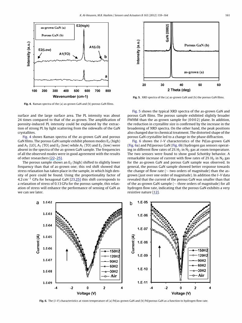
Fig. 3. Photoluminescence spectra of the (a) as-grown GaN and (b) the porous GaNfilms.
placed in the chamber with wires connected from the probes tothe Keithley model 2400 for measuring the current–voltage (I–V)characteristics of the sample.
3. Results and discussion
Fig. 2 shows the SEM images of the as-grown and the porous GaNfilms. The as-grown GaN possessed a smooth surface morphology(Fig. 2a). On the other hand, the porous GaN sample (Fig. 2b) wasfound to have a uniform pores structure with two distinct sizes,the smallest ones were observed to be around 30–40 nm while thelargest were around 70–80 nm. The two structures propagate inthe surface forming an interconnected crystallographic network.One of the most important characteristics of porous semiconduc-tors layers is their porosity (P), which is defined as the fraction ofvoid in the porous structure given by [21].
P = W1 − W2
W1 − W3(1)
where W1, W2 and W3 denote the weight of the original, anodized,and stripped wafer, respectively. In our work, the measured poros-ity P was 53%.
Fig. 3 shows the room temperature photoluminescence (PL)
spectra of the as-grown and the porous GaN films. The intensityof emitted lights is proportional to the number of photons emit-ted. This means that the number of photons emission is muchhigher for porous GaN than as-grown GaN, due to roughness of theGaN and (b) porous GaN films.
K. Al-Heuseen, M.R. Hashim / Sensors and Actuators B 163 (2012) 159– 164 161
s2ptc
Gaaoo
fss4aaw
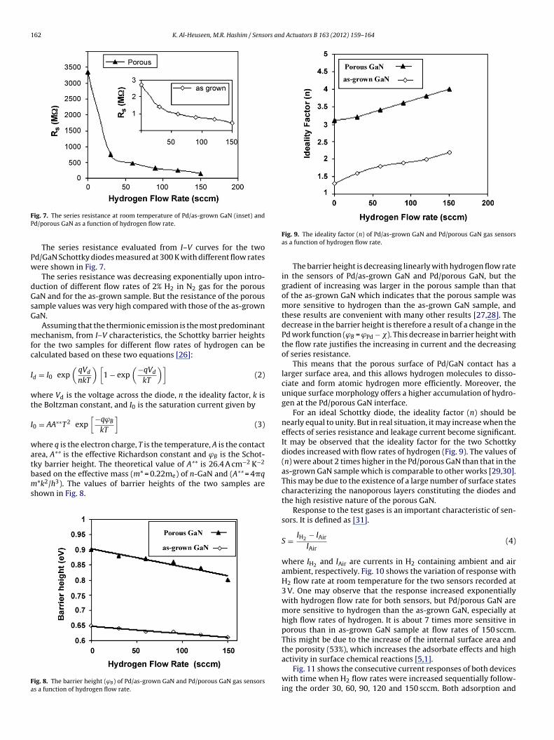
Fig. 4. Raman spectra of the (a) as-grown GaN and (b) porous GaN films.
urface and the large surface area. The PL intensity was about4 times compared to that of the as-grown. The amplification oforosity-induced PL intensity could be explained by the extrac-ion of strong PL by light scattering from the sidewalls of the GaNrystallites.
Fig. 4 shows Raman spectra of the as-grown GaN and porousaN films. The porous GaN sample exhibit phonon modes E2 (high)nd A1 (LO), A1 (TO) and E2 (low) while A1 (TO) and E2 (low) werebsent in the spectra of the as-grown GaN sample. The frequenciesf all the observed modes were in good agreement with the resultsf other researchers [22–25].
The porous sample shows an E2 (high) shifted to slightly lowerrequency than that of as-grown one; this red shift showed thattress relaxation has taken place in the sample, in which high den-ity of pore could be found. Using the proportionality factor of.2 cm−1 GPa for hexagonal GaN [23,25] this shift corresponds to
relaxation of stress of 0.13 GPa for the porous sample, this relax-tion of stress will enhance the performance of sensing of GaN ase can see later.
Fig. 6. The (I–V) characteristics at room temperature of (a) Pd/as-grown
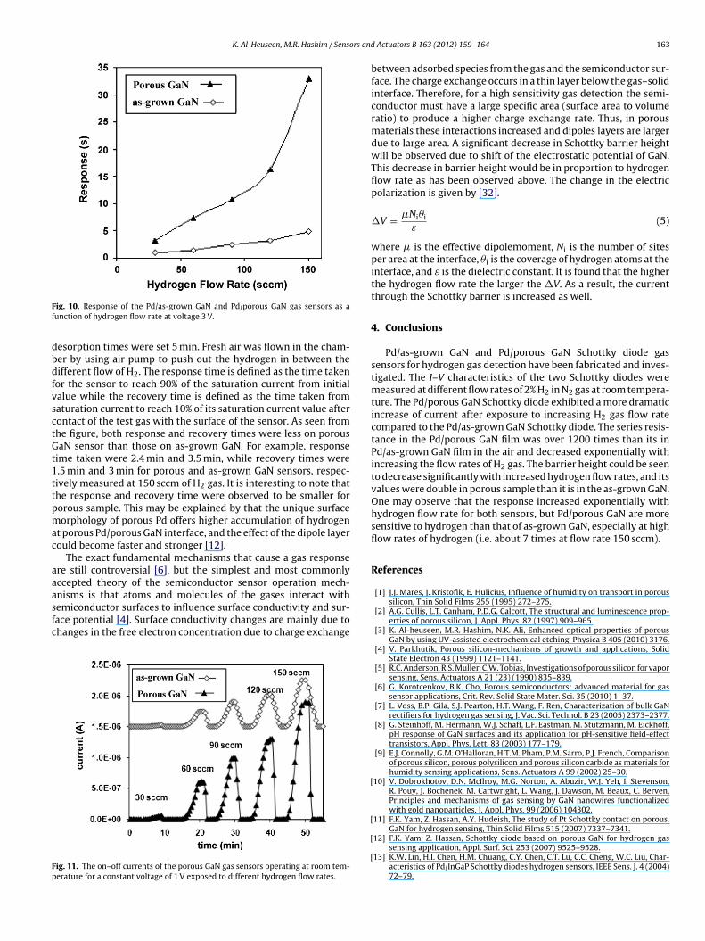
Fig. 5. XRD spectra of the (a) as-grown GaN and (b) the porous GaN films.
Fig. 5 shows the typical XRD spectra of the as-grown GaN andporous GaN films. The porous sample exhibited slightly broaderFWHM than the as-grown sample for (0 0 0 2) plane. In addition,the reduction in crystallite size is confirmed by the increase in thebroadening of XRD spectra. On the other hand, the peak positionsalso changed due to chemical treatment. The distorted shape of theporous GaN crystallite led to a change in the phase diffraction.
Fig. 6 shows the I–V characteristics of the Pd/as-grown GaN(Fig. 6a) and Pd/porous GaN (Fig. 6b) hydrogen gas sensors operat-ing in different flow rates of 2% H2 in N2 gas at room temperature.The two sensors were found to show good Schottky behavior. Aremarkable increase of current with flow rates of 2% H2 in N2 gasfor the as-grown GaN and porous GaN sample was observed. Ingeneral, the porous GaN sample showed better response towardsthe change of flow rate (∼ two orders of magnitude) than the as-grown (just over one order of magnitude). In addition the I–V datarevealed that the current of the porous GaN was smaller than that
of the as-grown GaN sample (∼ three orders of magnitude) for allhydrogen flow rate, indicating that the porous GaN exhibits a veryresistive nature [12].GaN and (b) Pd/porous GaN as a function to hydrogen flow rate.
162 K. Al-Heuseen, M.R. Hashim / Sensors and Actuators B 163 (2012) 159– 164
FP
Pw
dGsG
mfc
I
wt
I
watbms
Fa
ig. 7. The series resistance at room temperature of Pd/as-grown GaN (inset) andd/porous GaN as a function of hydrogen flow rate.
The series resistance evaluated from I–V curves for the twod/GaN Schottky diodes measured at 300 K with different flow ratesere shown in Fig. 7.
The series resistance was decreasing exponentially upon intro-uction of different flow rates of 2% H2 in N2 gas for the porousaN and for the as-grown sample. But the resistance of the porousample values was very high compared with those of the as-grownaN.
Assuming that the thermionic emission is the most predominantechanism, from I–V characteristics, the Schottky barrier heights
or the two samples for different flow rates of hydrogen can bealculated based on these two equations [26]:
d = I0 exp(
qVd
nkT
) [1 − exp
(−qVd
kT
)](2)
here Vd is the voltage across the diode, n the ideality factor, k ishe Boltzman constant, and I0 is the saturation current given by
0 = AA∗∗T2 exp[−qϕB
kT
](3)
here q is the electron charge, T is the temperature, A is the contactrea, A** is the effective Richardson constant and ϕB is the Schot-ky barrier height. The theoretical value of A** is 26.4 A cm−2 K−2
ased on the effective mass (m* = 0.22me) of n-GaN and (A** = 4�q*k2/h3). The values of barrier heights of the two samples are
hown in Fig. 8.
ig. 8. The barrier height (ϕB) of Pd/as-grown GaN and Pd/porous GaN gas sensorss a function of hydrogen flow rate.
Fig. 9. The ideality factor (n) of Pd/as-grown GaN and Pd/porous GaN gas sensorsas a function of hydrogen flow rate.
The barrier height is decreasing linearly with hydrogen flow ratein the sensors of Pd/as-grown GaN and Pd/porous GaN, but thegradient of increasing was larger in the porous sample than thatof the as-grown GaN which indicates that the porous sample wasmore sensitive to hydrogen than the as-grown GaN sample, andthese results are convenient with many other results [27,28]. Thedecrease in the barrier height is therefore a result of a change in thePd work function (ϕB = ϕPd − �). This decrease in barrier height withthe flow rate justifies the increasing in current and the decreasingof series resistance.
This means that the porous surface of Pd/GaN contact has alarger surface area, and this allows hydrogen molecules to disso-ciate and form atomic hydrogen more efficiently. Moreover, theunique surface morphology offers a higher accumulation of hydro-gen at the Pd/porous GaN interface.
For an ideal Schottky diode, the ideality factor (n) should benearly equal to unity. But in real situation, it may increase when theeffects of series resistance and leakage current become significant.It may be observed that the ideality factor for the two Schottkydiodes increased with flow rates of hydrogen (Fig. 9). The values of(n) were about 2 times higher in the Pd/porous GaN than that in theas-grown GaN sample which is comparable to other works [29,30].This may be due to the existence of a large number of surface statescharacterizing the nanoporous layers constituting the diodes andthe high resistive nature of the porous GaN.
Response to the test gases is an important characteristic of sen-sors. It is defined as [31].
S = IH2 − IAir
IAir(4)
where IH2 and IAir are currents in H2 containing ambient and airambient, respectively. Fig. 10 shows the variation of response withH2 flow rate at room temperature for the two sensors recorded at3 V. One may observe that the response increased exponentiallywith hydrogen flow rate for both sensors, but Pd/porous GaN aremore sensitive to hydrogen than the as-grown GaN, especially athigh flow rates of hydrogen. It is about 7 times more sensitive inporous than in as-grown GaN sample at flow rates of 150 sccm.This might be due to the increase of the internal surface area andthe porosity (53%), which increases the adsorbate effects and high
activity in surface chemical reactions [5,1].Fig. 11 shows the consecutive current responses of both deviceswith time when H2 flow rates were increased sequentially follow-ing the order 30, 60, 90, 120 and 150 sccm. Both adsorption and
K. Al-Heuseen, M.R. Hashim / Sensors and
Ff
dbdfvsctGt1ttpmac
aaasfc
Fp
ig. 10. Response of the Pd/as-grown GaN and Pd/porous GaN gas sensors as aunction of hydrogen flow rate at voltage 3 V.
esorption times were set 5 min. Fresh air was flown in the cham-er by using air pump to push out the hydrogen in between theifferent flow of H2. The response time is defined as the time takenor the sensor to reach 90% of the saturation current from initialalue while the recovery time is defined as the time taken fromaturation current to reach 10% of its saturation current value afterontact of the test gas with the surface of the sensor. As seen fromhe figure, both response and recovery times were less on porousaN sensor than those on as-grown GaN. For example, response
ime taken were 2.4 min and 3.5 min, while recovery times were.5 min and 3 min for porous and as-grown GaN sensors, respec-ively measured at 150 sccm of H2 gas. It is interesting to note thathe response and recovery time were observed to be smaller fororous sample. This may be explained by that the unique surfaceorphology of porous Pd offers higher accumulation of hydrogen
t porous Pd/porous GaN interface, and the effect of the dipole layerould become faster and stronger [12].
The exact fundamental mechanisms that cause a gas responsere still controversial [6], but the simplest and most commonlyccepted theory of the semiconductor sensor operation mech-nisms is that atoms and molecules of the gases interact with
emiconductor surfaces to influence surface conductivity and sur-ace potential [4]. Surface conductivity changes are mainly due tohanges in the free electron concentration due to charge exchangeig. 11. The on–off currents of the porous GaN gas sensors operating at room tem-erature for a constant voltage of 1 V exposed to different hydrogen flow rates.
[
[
[
[
Actuators B 163 (2012) 159– 164 163
between adsorbed species from the gas and the semiconductor sur-face. The charge exchange occurs in a thin layer below the gas–solidinterface. Therefore, for a high sensitivity gas detection the semi-conductor must have a large specific area (surface area to volumeratio) to produce a higher charge exchange rate. Thus, in porousmaterials these interactions increased and dipoles layers are largerdue to large area. A significant decrease in Schottky barrier heightwill be observed due to shift of the electrostatic potential of GaN.This decrease in barrier height would be in proportion to hydrogenflow rate as has been observed above. The change in the electricpolarization is given by [32].
�V = �Ni�i
ε(5)
where � is the effective dipolemoment, Ni is the number of sitesper area at the interface, �i is the coverage of hydrogen atoms at theinterface, and ε is the dielectric constant. It is found that the higherthe hydrogen flow rate the larger the �V. As a result, the currentthrough the Schottky barrier is increased as well.
4. Conclusions
Pd/as-grown GaN and Pd/porous GaN Schottky diode gassensors for hydrogen gas detection have been fabricated and inves-tigated. The I–V characteristics of the two Schottky diodes weremeasured at different flow rates of 2% H2 in N2 gas at room tempera-ture. The Pd/porous GaN Schottky diode exhibited a more dramaticincrease of current after exposure to increasing H2 gas flow ratecompared to the Pd/as-grown GaN Schottky diode. The series resis-tance in the Pd/porous GaN film was over 1200 times than its inPd/as-grown GaN film in the air and decreased exponentially withincreasing the flow rates of H2 gas. The barrier height could be seento decrease significantly with increased hydrogen flow rates, and itsvalues were double in porous sample than it is in the as-grown GaN.One may observe that the response increased exponentially withhydrogen flow rate for both sensors, but Pd/porous GaN are moresensitive to hydrogen than that of as-grown GaN, especially at highflow rates of hydrogen (i.e. about 7 times at flow rate 150 sccm).
References
[1] J.J. Mares, J. Kristofik, E. Hulicius, Influence of humidity on transport in poroussilicon, Thin Solid Films 255 (1995) 272–275.
[2] A.G. Cullis, L.T. Canham, P.D.G. Calcott, The structural and luminescence prop-erties of porous silicon, J. Appl. Phys. 82 (1997) 909–965.
[3] K. Al-heuseen, M.R. Hashim, N.K. Ali, Enhanced optical properties of porousGaN by using UV-assisted electrochemical etching, Physica B 405 (2010) 3176.
[4] V. Parkhutik, Porous silicon-mechanisms of growth and applications, SolidState Electron 43 (1999) 1121–1141.
[5] R.C. Anderson, R.S. Muller, C.W. Tobias, Investigations of porous silicon for vaporsensing, Sens. Actuators A 21 (23) (1990) 835–839.
[6] G. Korotcenkov, B.K. Cho, Porous semiconductors: advanced material for gassensor applications, Crit. Rev. Solid State Mater. Sci. 35 (2010) 1–37.
[7] L. Voss, B.P. Gila, S.J. Pearton, H.T. Wang, F. Ren, Characterization of bulk GaNrectifiers for hydrogen gas sensing, J. Vac. Sci. Technol. B 23 (2005) 2373–2377.
[8] G. Steinhoff, M. Hermann, W.J. Schaff, L.F. Eastman, M. Stutzmann, M. Eickhoff,pH response of GaN surfaces and its application for pH-sensitive field-effecttransistors, Appl. Phys. Lett. 83 (2003) 177–179.
[9] E.J. Connolly, G.M. O’Halloran, H.T.M. Pham, P.M. Sarro, P.J. French, Comparisonof porous silicon, porous polysilicon and porous silicon carbide as materials forhumidity sensing applications, Sens. Actuators A 99 (2002) 25–30.
10] V. Dobrokhotov, D.N. McIlroy, M.G. Norton, A. Abuzir, W.J. Yeh, I. Stevenson,R. Pouy, J. Bochenek, M. Cartwright, L. Wang, J. Dawson, M. Beaux, C. Berven,Principles and mechanisms of gas sensing by GaN nanowires functionalizedwith gold nanoparticles, J. Appl. Phys. 99 (2006) 104302.
11] F.K. Yam, Z. Hassan, A.Y. Hudeish, The study of Pt Schottky contact on porous.GaN for hydrogen sensing, Thin Solid Films 515 (2007) 7337–7341.
12] F.K. Yam, Z. Hassan, Schottky diode based on porous GaN for hydrogen gassensing application, Appl. Surf. Sci. 253 (2007) 9525–9528.
13] K.W. Lin, H.I. Chen, H.M. Chuang, C.Y. Chen, C.T. Lu, C.C. Cheng, W.C. Liu, Char-acteristics of Pd/InGaP Schottky diodes hydrogen sensors, IEEE Sens. J. 4 (2004)72–79.
1 rs and
[
[
[
[
[
[
[
[
[
[
[
[
[
[
[
[
[
[
[
64 K. Al-Heuseen, M.R. Hashim / Senso
14] L. Mazet, C. Varenne, A. Pauly, J. Brunet, J.P. Germain, H2, CO and high vac-uum regeneration of ozone poisoned pseudo-Schottky Pd–InP based gas sensor,Sens. Actuators B 103 (2004) 190–199.
15] J.S. Wright, W. Lima, B.P. Gilaa, S.J. Peartona, J.L. Johnsonb, A. Ural, F. Renc,Hydrogen sensing with Pt-functionalized GaN nanowires, Sens. Actuators B140 (2009) 196–203.
16] A. Salehi, A. Nikfarjam, D.J. Kalantari, Pd/porous-GaAs Schottky contact forhydrogen sensing application, Sens. Actuators B 113 (2006) 419–427.
17] V.G. Litovchenko, T.I. Gorbanyuk, V.S. Solntsev, A.A. Evtukh, Mechanism ofhydrogen, oxygen and humidity sensing by Cu/Pd-porous silicon-silicon struc-tures, Appl. Surf. Sci. 234 (2004) 262–267.
18] A. Salehi, D.J. Kalantari, Characteristics of highly sensitive Au/porous-GaAsSchottky junctions as selective CO and NO gas sensors, Sens. Actuators B 122(2007) 69–74.
19] L. Pancheri, C.J. Oton, Z. Gaburro, G. Soncini, L. Pavesi, Very sensitive poroussilicon NO2 sensor, Sens. Actuators B 89 (2003) 237–239.
20] W.M. Kwok, Y.C. Bow, W.Y. Chan, M.C. Poon, P.G. Wan, H. Wong, Proceedingsof Electron Devices Meeting, IEEE, Hong Kong, vol. 80, 1999.
21] C. Vinegoni, M. Cazzanelli, L. Pavesi, Silicon-based materials and devices, in: H.S.Nalwa (Ed.), Properties and Devices, vol. 2, Academic Press, 2001, pp. 123–192.
22] H. Hartono, C.B. Soh, S.J. Chua, E.A. Fitzgerald, Annihilation of threading disloca-tions in strain relaxed nano-porous GaN template for high quality GaN growth,Phys. Stat. Sol. 4 (2007) 2572–2575.
23] C. Kisielowski, J. Krüger, S. Ruvimov, T. Suski, J.W. Ager, E. Jones, Z. Liliental-Weber, M. Rubin, E.R. Weber, M.D. Bremser, R.F. Davis, Strain relatedphenomena in GaN thin films, Phys. Rev. B 54 (1996) 17745–177753.
24] A.P. Vajpeyi, S.J. Chua, S. Tripathy, E.A. Fitzgerald, W. Liu, P. Chen, L.S. Wang, Highoptical quality nanoporous GaN prepared by photoelectrochemical etching,Electrochem. Solid State Lett. 8 (2005) G85–G88.
25] F.Y. Yam, Z. Hassan, Structural and optical characteristics of porous GaN gen-erated by electroless chemical etching, Mater. Lett. 63 (2009) 724–727.
26] V.L. Rideout, A review of the theory and technology for ohmic contactsto group III-V compound semiconductors, Solid State Electron. 18 (1975)541–545.
27] S.N. Das, A.K. Pal1, Hydrogen sensor based on thin film nanocrystalline n-GaN/Pd Schottky diode, J. Phys. D: Appl. Phys. 40 (2007) 7291–7297.
28] A. Ramizy, Z. Hassan, K. Omar, Porous GaN on Si (1 1 1) and its application tohydrogen gas sensor, Sens. Actuators B 155 (2011) 699–708.
29] J.M. Shah, Y.L. Li, T. Gessmann, E.F. Schubert, Experimental analysis and theo-retical model for anomalously high ideality factors (n � 2.0) in AlGaN/GaN p–njunction diodes, J. Appl. Phys. 94 (2003) 2627–2631.
Actuators B 163 (2012) 159– 164
30] H. Colder, R. Rizk, L. Pichon, O. Bonnaud, Low-temperature processing and prop-erties of nanocrystalline-SiC/crystalline Si heterojunction devices, Solid StateElectron. 50 (2006) 209–213.
31] J. Song, W. Lu, J.S. Flynn, G.R. Brandes, Pt-AlGaN/GaN Schottky diodes operatedat 800 ◦C for hydrogen sensing, Appl. Phys. Lett. 87 (2005) 133501–133504.
32] M. Johansson, I. Lundstrom, L.G. Ekedahl, Bridging the pressure gap for palla-dium metal–insulator–semiconductor hydrogen sensors in oxygen containingenvironments, J. Appl. Phys. 84 (1998) 44–54.
Biographies
Khalled Al-Heuseen received the B.Sc. degree and the Masters degree in physics,both from the Yarmouk University Jordan in 1990 and 1993, respectively. Hereceived his PhD degree in 2011 from the Universiti sains Malaysia. Currently, he isa university lecturer in Al-Balqa’, Applied University, Ajloun University College, Jor-dan. Participated in many national and international conferences and workshopsand published 12 papers in ISI journals. Research interested in nanostructuredmaterials and their applications, using low cost conventional techniques namelyelectrochemical deposition and etching.
Md. Roslan Hashim, Ph.D., received the B.Sc. (Hons) in Physics and M.Sc. in AppliedPhysics (Optoelectronics) both from the Universiti Sains Malaysia in 1989 and 1993,respectively. His M.Sc. work was developing fast Fourier transform spectrometersystem to study the optical properties of the strained and unstrained group IV andIII–V semiconductors. He received his PhD degree in 1997 from the University ofSouthampton, England. His dissertation topic was characterization, developmentand modeling of high-speed SiGe hetero-junction bipolar transistors. Currently,he is an Professor, and working in the Solid State and Applied Physics Group atthe School of Physics, Universiti Sains Malaysia, Penang. He is also the Chairmanof Applied Physics Program for undergraduates. He has received several awardsincluding Graduate Scholarship from USM, Excellent Performance Awards, SanggarSanjung (Hall of Fame) and Merit Awards. His main research interest is on semicon-ductor nanostructures studies fabricated using low cost conventional techniquesnamely electrochemical deposition and etching as well as thermal evaporation. He
has published more than 120 papers in international and national journals and pro-ceedings. He reviewed few high impact factor international journals such as Journalof Physics D; Applied Physics, Electrochemical and Solid State Letters, Nanotechnologyand Semiconductor Science and Technology. He is a member of Malaysian Solid StateScience and Technology Society.
Related Documents