NANO EXPRESS Open Access Si nanopatterning by reactive ion etching through an on-chip self-assembled porous anodic alumina mask Violetta Gianneta, Antonis Olziersky and Androula G Nassiopoulou * Abstract We report on Si nanopatterning through an on-chip self-assembled porous anodic alumina (PAA) masking layer using reactive ion etching based on fluorine chemistry. Three different gases/gas mixtures were investigated: pure SF 6 , SF 6 /O 2 , and SF 6 /CHF 3 . For the first time, a systematic investigation of the etch rate and process anisotropy was performed. It was found that in all cases, the etch rate through the PAA mask was 2 to 3 times lower than that on non-masked areas. With SF 6 , the etching process is, as expected, isotropic. By the addition of O 2 , the etch rate does not significantly change, while anisotropy is slightly improved. The lowest etch rate and the best anisotropy were obtained with the SF 6 /CHF 3 gas mixture. The pattern of the hexagonally arranged pores of the alumina film is, in this case, perfectly transferred to the Si surface. This is possible both on large areas and on restricted pre-defined areas on the Si wafer. Keywords: Porous anodic alumina, Si nanopatterning, Reactive ion etching, Fluorine chemistry PACS: 78.67.Rb, 81.07.-b, 61.46.-w Background Si nanopatterning finds important applications in nanoelectronics, photonics, and sensors. Advanced tech- niques as electron beam lithography or focused ion beam milling can be used in this respect; however, they are both expensive and time consuming when large areas have to be patterned. The use of a masking layer either on the whole wafer or locally on pre-defined areas on the Si substrate can provide a good and cost-effective alternative to the above techniques. Porous anodic alumina (PAA) thin films on Si offer important possibil- ities in this respect. PAA films can be fabricated on the Si wafer by electrochemical oxidation of a thin Al film deposited on the Si surface by physical vapor deposition. The so-formed aluminum oxide (alumina) shows highly ordered vertical pores that can reach the Si substrate and can be used either as a masking layer for Si nanopatterning [1-4] or as a template for nanowire and nanocrystal growth within the pores. PAA films can be also used as the dielec- tric material in metal-oxide-metal (MIM) capacitors [5-7] and as the charging medium in non-volatile memory devices [8]. PAA films can be formed either on large areas or on pre-selected small areas of the Si wafer. This is very useful in all the above applications. In Si nanopatterning, the Al film is first patterned and is then anodized to form the PAA mask. It is thus possible to pattern both small areas and very large areas on the Si wafer. Perfectly hexagonal self-ordered PAA films were first reported on Al foils by Masuda and Fukuda in 1995 [9]. Other works then followed, which focused on the vari- ation of the main properties of such ordered PAA films, i.e., the cell size, pore diameter, and pore depth as a function of the anodization conditions (i.e., the acidic solution, the anodization voltage, and the anodization time used [10-12]). For a perfect masking technology for Si nanopatterning, the development of optimized PAA films with tunable pore size and density on the Si wafer are needed. Perfect PAA layers are easily achieved on an Al foil [13,14]. After their release from the Al substrate, free standing PAA membranes are fabricated. Such membranes were used in the literature for Si nanopatterning [15]. However, the direct formation of the PAA mask on the Si substrate * Correspondence: [email protected] NCSR Demokritos/IMEL, Terma Patriarhou Gregoriou, Aghia Paraskevi, Athens 15310, Greece © 2013 Gianneta et al.; licensee Springer. This is an Open Access article distributed under the terms of the Creative Commons Attribution License (http://creativecommons.org/licenses/by/2.0), which permits unrestricted use, distribution, and reproduction in any medium, provided the original work is properly cited. Gianneta et al. Nanoscale Research Letters 2013, 8:71 http://www.nanoscalereslett.com/content/8/1/71

Welcome message from author
This document is posted to help you gain knowledge. Please leave a comment to let me know what you think about it! Share it to your friends and learn new things together.
Transcript

Gianneta et al. Nanoscale Research Letters 2013, 8:71http://www.nanoscalereslett.com/content/8/1/71
NANO EXPRESS Open Access
Si nanopatterning by reactive ion etchingthrough an on-chip self-assembled porous anodicalumina maskVioletta Gianneta, Antonis Olziersky and Androula G Nassiopoulou*
Abstract
We report on Si nanopatterning through an on-chip self-assembled porous anodic alumina (PAA) masking layerusing reactive ion etching based on fluorine chemistry. Three different gases/gas mixtures were investigated: pureSF6, SF6/O2, and SF6/CHF3. For the first time, a systematic investigation of the etch rate and process anisotropy wasperformed. It was found that in all cases, the etch rate through the PAA mask was 2 to 3 times lower than that onnon-masked areas. With SF6, the etching process is, as expected, isotropic. By the addition of O2, the etch rate doesnot significantly change, while anisotropy is slightly improved. The lowest etch rate and the best anisotropy wereobtained with the SF6/CHF3 gas mixture. The pattern of the hexagonally arranged pores of the alumina film is, inthis case, perfectly transferred to the Si surface. This is possible both on large areas and on restricted pre-definedareas on the Si wafer.
Keywords: Porous anodic alumina, Si nanopatterning, Reactive ion etching, Fluorine chemistry
PACS: 78.67.Rb, 81.07.-b, 61.46.-w
BackgroundSi nanopatterning finds important applications innanoelectronics, photonics, and sensors. Advanced tech-niques as electron beam lithography or focused ionbeam milling can be used in this respect; however, theyare both expensive and time consuming when largeareas have to be patterned. The use of a masking layereither on the whole wafer or locally on pre-defined areason the Si substrate can provide a good and cost-effectivealternative to the above techniques. Porous anodicalumina (PAA) thin films on Si offer important possibil-ities in this respect. PAA films can be fabricated on theSi wafer by electrochemical oxidation of a thin Al filmdeposited on the Si surface by physical vapor deposition.The so-formed aluminum oxide (alumina) shows highlyordered vertical pores that can reach the Si substrate andcan be used either as a masking layer for Si nanopatterning[1-4] or as a template for nanowire and nanocrystal growthwithin the pores. PAA films can be also used as the dielec-tric material in metal-oxide-metal (MIM) capacitors [5-7]
* Correspondence: [email protected] Demokritos/IMEL, Terma Patriarhou Gregoriou, Aghia Paraskevi, Athens15310, Greece
© 2013 Gianneta et al.; licensee Springer. This iAttribution License (http://creativecommons.orin any medium, provided the original work is p
and as the charging medium in non-volatile memorydevices [8]. PAA films can be formed either on large areasor on pre-selected small areas of the Si wafer. This is veryuseful in all the above applications. In Si nanopatterning,the Al film is first patterned and is then anodized to formthe PAA mask. It is thus possible to pattern both smallareas and very large areas on the Si wafer.Perfectly hexagonal self-ordered PAA films were first
reported on Al foils by Masuda and Fukuda in 1995 [9].Other works then followed, which focused on the vari-ation of the main properties of such ordered PAA films,i.e., the cell size, pore diameter, and pore depth as afunction of the anodization conditions (i.e., the acidicsolution, the anodization voltage, and the anodizationtime used [10-12]).For a perfect masking technology for Si nanopatterning,
the development of optimized PAA films with tunablepore size and density on the Si wafer are needed. PerfectPAA layers are easily achieved on an Al foil [13,14]. Aftertheir release from the Al substrate, free standing PAAmembranes are fabricated. Such membranes were used inthe literature for Si nanopatterning [15]. However, thedirect formation of the PAA mask on the Si substrate
s an Open Access article distributed under the terms of the Creative Commonsg/licenses/by/2.0), which permits unrestricted use, distribution, and reproductionroperly cited.

Figure 1 Examples of SEM images of a PAA film on Si. Thespecific PAA film on Si was fabricated by anodic oxidation of an Alfilm/Si in oxalic acid aqueous solution, using two-step anodization.Images (a) and (b), and the inset of (b) are top view images, while(c) depicts a cross-sectional image. The pore diameter in this sampleis approximately 40 nm after pore widening for a durationof 40 min.
Gianneta et al. Nanoscale Research Letters 2013, 8:71 Page 2 of 7http://www.nanoscalereslett.com/content/8/1/71
offers more flexibility in the etching process than freestanding PAA membranes. The structural difference ofPAA films on Si compared with similar films on an Al foilis mainly at the interface with the Si substrate. Anodizationof the film on Si proceeds as in the case of the Al foil untilthe so-called barrier layer of the alumina film reaches the Sisurface. At this stage, the barrier layer at each pore bottom
Table 1 Characteristics of the PAA layers in the threedifferent samples used in this work
PAA thickness(nm)
Pore size in nm afterpore widening for 40 min
Annealing
Sample 1 390 35 – 45 No
Sample 2 560 35 – 55 Yes
Sample 3 400 35 – 45 Yes
is detached from the rigid Si substrate under mechanicalstress, forming a thin capping layer over a void at each porebase [16,17]. After the void and capping layer formation, ifthe electrochemical process is not stopped, it proceeds byoxidizing the Si surface, starting from the pore walls andcontinuing to fully oxidize the Si surface underneath thePAA film. In most of the applications, the anodization hasto be stopped just after full Al consumption. The barrierlayer at each pore bottom has to be removed so as to getpores that reach the Si surface.In this paper, we applied optimized PAA thin films on
Si with regular long range pore arrangement and weinvestigated the pattern transfer to the Si wafer using re-active ion etching (RIE) with three different fluorine gasmixtures: pure SF6, SF6/O2, and SF6/CHF3.
MethodsPAA films used in this work were fabricated by anodicoxidation of an Al film, deposited on Si by electron gunevaporation. The electrolyte used was an aqueous solutionof oxalic acid, 5 w.t.%, and the process was carried out at1-2°C and a constant voltage of 40 V.An example of field emission scanning electron mi-
croscopy (SEM) images of a PAA film on Si fabricatedby anodizing a 750-nm thick Al film as described aboveis shown in Figure 1. In Figure 1a, a plane view SEMimage of the surface of the as-formed film is depicted,while in Figure 1b, we see a larger area SEM image ofthe same film after pore widening for 40 min in 0.86 Mphosphoric acid. The same film is shown in higher mag-nification in the inset of Figure 1b, where the hexagonalpore arrangement is clearly depicted and schematicallyidentified in the image.The pore widening process is performed after the end
of the anodic oxidation by immersion of the samples ina 0.86 M phosphoric acid aqueous solution. This processresults in partial dissolution of the pore inner wall sur-face and in the dissolution of the inverted barrier layerat the base of each pore.In order to improve long range pore ordering of the
PAA film, a two-step anodization process was applied inall cases. This process starts with a thick Al film, andpart of it is consumed by anodization and alumina dis-solution. Pore initiation sites for the second anodizationstep are thus formed, which help obtain perfect longrange pore ordering of the PAA film.
Pattern transfer to the Si substrateGeneralNanopatterning of Si through self-assembled porous anodicaluminum oxide thin films is an interesting lithography-freeprocess for fabricating regular nanoscale patterns on the Siwafer. The area to be patterned can be pre-selected bypatterning the Al thin film, which is then anodized using
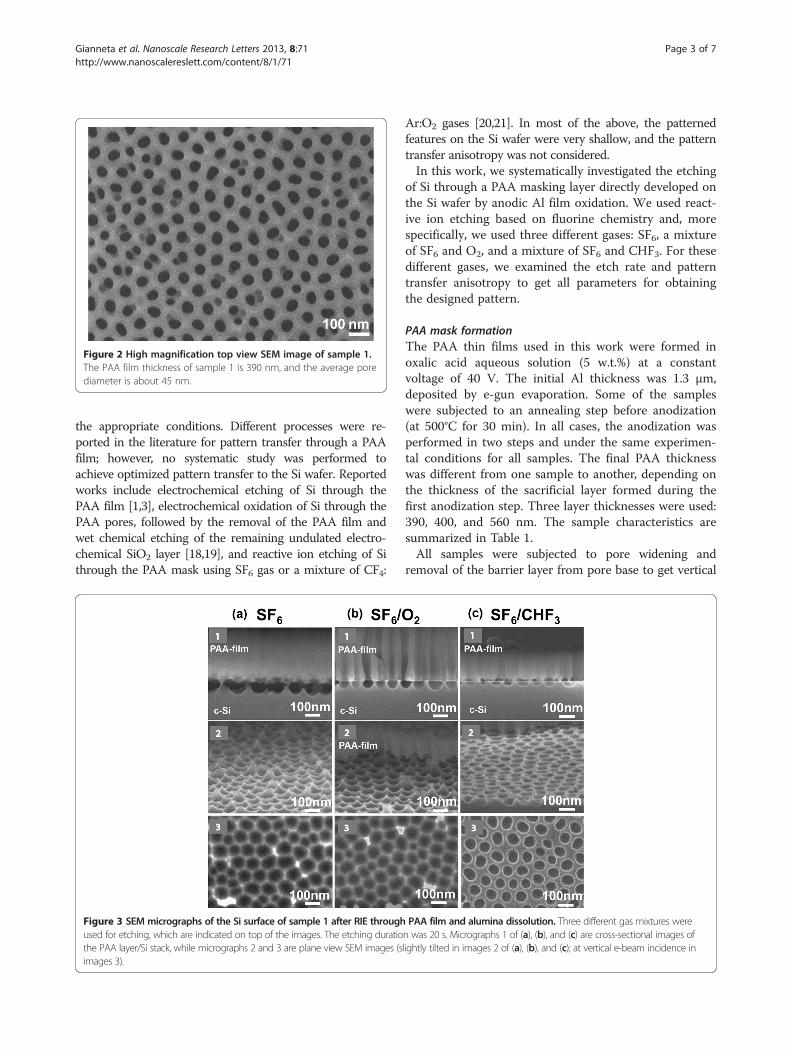
Figure 2 High magnification top view SEM image of sample 1.The PAA film thickness of sample 1 is 390 nm, and the average porediameter is about 45 nm.
Gianneta et al. Nanoscale Research Letters 2013, 8:71 Page 3 of 7http://www.nanoscalereslett.com/content/8/1/71
the appropriate conditions. Different processes were re-ported in the literature for pattern transfer through a PAAfilm; however, no systematic study was performed toachieve optimized pattern transfer to the Si wafer. Reportedworks include electrochemical etching of Si through thePAA film [1,3], electrochemical oxidation of Si through thePAA pores, followed by the removal of the PAA film andwet chemical etching of the remaining undulated electro-chemical SiO2 layer [18,19], and reactive ion etching of Sithrough the PAA mask using SF6 gas or a mixture of CF4:
Figure 3 SEM micrographs of the Si surface of sample 1 after RIE throughused for etching, which are indicated on top of the images. The etching duratiothe PAA layer/Si stack, while micrographs 2 and 3 are plane view SEM images (simages 3).
Ar:O2 gases [20,21]. In most of the above, the patternedfeatures on the Si wafer were very shallow, and the patterntransfer anisotropy was not considered.In this work, we systematically investigated the etching
of Si through a PAA masking layer directly developed onthe Si wafer by anodic Al film oxidation. We used react-ive ion etching based on fluorine chemistry and, morespecifically, we used three different gases: SF6, a mixtureof SF6 and O2, and a mixture of SF6 and CHF3. For thesedifferent gases, we examined the etch rate and patterntransfer anisotropy to get all parameters for obtainingthe designed pattern.
PAA mask formationThe PAA thin films used in this work were formed inoxalic acid aqueous solution (5 w.t.%) at a constantvoltage of 40 V. The initial Al thickness was 1.3 μm,deposited by e-gun evaporation. Some of the sampleswere subjected to an annealing step before anodization(at 500°C for 30 min). In all cases, the anodization wasperformed in two steps and under the same experimen-tal conditions for all samples. The final PAA thicknesswas different from one sample to another, depending onthe thickness of the sacrificial layer formed during thefirst anodization step. Three layer thicknesses were used:390, 400, and 560 nm. The sample characteristics aresummarized in Table 1.All samples were subjected to pore widening and
removal of the barrier layer from pore base to get vertical
PAA film and alumina dissolution. Three different gas mixtures weren was 20 s. Micrographs 1 of (a), (b), and (c) are cross-sectional images oflightly tilted in images 2 of (a), (b), and (c); at vertical e-beam incidence in

Figure 4 SEM micrographs of sample 1 after RIE in twodifferent gas mixtures. Micrographs 1 of (a) and (b) are cross-sectional images, while images 2 and 3 of (a) and (b) are plane viewimages. Etching was performed in SF6/O2 (images 1 to 3 of (a)) andin SF6/CHF3 (images 1 to 3 of (b)). The etching duration was 40 s inimages 1 and 2, and 60 s in images 3. In the cross-sectional images,the PAA mask is present; in the plane view images, it is removed,revealing the nanopatterned Si surface.
Figure 5 Plane view SEM images of the Si surface of sample 1.The images show the nanopatterned Si surface of sample 1 afteretching through the PAA mask using SF6/CHF3 gas mixture for 20 s(a), 40 s (b), and 60s (c). The alumina film was removedbefore observation.
Gianneta et al. Nanoscale Research Letters 2013, 8:71 Page 4 of 7http://www.nanoscalereslett.com/content/8/1/71
pores that reach the Si substrate. An example of SEMimage of the surface of an optimized PAA film used in thiswork is depicted in Figure 2. In this sample, the Al filmwas not annealed before anodization. The average poresize was 45 nm, and the PAA film thickness was 390 nm.
Reactive ion etching of Si through the PAA maskThe mechanisms involved in reactive ion etching combinephysical (sputtering) and chemical etching. The gases ormixture of gases used and the RIE power and gas pressureare critical parameters that determine the etch rate. Theetch rate is also different on large Si surface areas com-pared to the etch rate through a mask with nanometricopenings. In this work, the PAA mask used showed he-xagonally arranged pores with size in the range of 30 to50 nm and interpore distance around 30 nm.Three different gases or gas mixtures were used: SF6
(25 sccm), a mixture of SF6/O2 (25 sccm/2.8 sccm), anda mixture of SF6/CHF3 (25 sccm/37.5 sccm). In the firstcase, the etching of Si is known to be isotropic, while inthe last two cases, it is more or less anisotropic. Separateexperiments were performed for each gas mixture. In allcases, we used three different etching times, namely, 20,
40, and 60 s. The conditions used for the RIE were asfollows: power 400 W and gas pressure 10 mTorr.An example of SEM image from sample 1 after RIE
for 20 s in the three different gases/gas mixtures isshown in Figure 3. Figure 3a corresponds to SF6 gas(image 1 is a cross-sectional image of the PAA/Si stack,

Figure 6 Cross-sectional SEM images of two samples. One non-annealed and one that was annealed in nitrogen gas beforeanodization. Cross-sectional view of sample 1 that was not annealed(images 1 of (a) and (b)) and sample 2 that was annealed at 500°Cfor 30 min in nitrogen gas before anodization for alumina formation(annealed; images 2 of (a) and (b)). Etching was performed for 20 sin SF6 (images 1 and 2 in (a)) and SF6/CHF3 (images 1 and 2 in(b)), respectively.
Figure 7 Alumina/Si interface of the Al-annealed sample. Cross-sectional SEM image of the interface PAA/Si of an Al-annealedsample at 500°C for 30 min in nitrogen gas. An undulation of theinterface is depicted, attributed to Al diffusion into Si (due to theannealing) before anodization.
Gianneta et al. Nanoscale Research Letters 2013, 8:71 Page 5 of 7http://www.nanoscalereslett.com/content/8/1/71
while images 2 and 3 are plane view images of thenanopatterned Si surface (image 2 at tilted, and 3 at nor-mal incidence) after the removal of the PAA film.Figure 3b,c corresponds to respective images using SF6/O2
and SF6/CHF3 gas mixtures. From the images, it is obvi-ous that the etch rate with the SF6 gas is higher than theetch rate with the two other gases, and as expected, theetching is isotropic, thus resulting in almost full release ofthe PAA thin film after RIE of the samples for 20 s. Thus,the nanopatterned Si surface after PAA removal showsquite shallow features. When adding O2 to SF6, theetching process is slowed down and is more anisotropic.As a result, the 20-s etch time does not lead to PAA maskrelease, but instead, a nanopatterned surface with featureswell separated by pore walls are formed (Figure 3b image1). When replacing O2 by CHF3, the RIE process is evenslower and more anisotropic, thus resulting in shalloweretched features at each pore bottom and thicker porewalls, as clearly depicted in Figure 3c.By increasing the etching time, the depth of the etched
holes at each pore bottom increases, but gradually, the lat-eral etching results in almost full etching of the inter-holewalls, starting from their top, and finally PAA membranerelease. This happens earlier with SF6 (isotropic etching)than with the other two gas mixtures. Figure 4 depicts theSEM images of sample 1 after etching in SF6/O2 (Figure 4a)and in SF6/CHF3 (Figure 4b) for 40 s (images 1 and 2 ofFigure 4a, and images 1 and 2 of Figure 4b) and 60 s(images 3 of Figure 4a,b). Already for 40-s etching time,the PAA film is fully released when using SF6/O2 gas mix-ture, and the Si inter-hole walls are reduced in height. With
SF6/CHF3 gas mixture, well-separated nanofeatures on Siare formed, with the inter-pore Si walls intact at their topsurface. Finally, for the 60-s etching time, the PAA layerwas fully released in both gas mixtures.Etching evolution with time in SF6/CHF3 is illustrated
by the SEM images of the nanopatterned Si surface afterthe removal of the PAA mask, depicted in Figure 5 for20-, 40- and 60-s etching time. Due to the reduced etchrate and process anisotropy, pattern formation is morecontrollable than with the SF6 or SF6/O2.
Effect of Al annealing before anodizationGood adhesion of the Al film with Si is important forobtaining a sharp interface between the PAA film and Si.The adhesion of the PAA film with Si is an importantparameter for achieving etching anisotropy. If adhesionis not good, the reactive gases enter underneath thePAA mask through the alumina pores and start to etchthe whole Si surface, resulting in mask release. In orderto avoid this effect, an annealing step of the Al film at500°C for 30 min before electrochemical oxidation wasused in samples 2 and 3. The effect of Al annealingis illustrated in Figure 6 by comparing sample 1 (non-annealed; images 1 of (a) and (b)) with sample2 (annealed; Figure 6, images 2 of (a) and (b)) afteretching for 20 s in SF6 (Figure 6, images 1 and 2 of (a))and SF6/CHF3 (Figure 6, images 1 and 2 of (b)), respect-ively. We observe that in the case of the non-annealedsample, there is a full detachment of the PAA mask inSF6 gas and partial detachment in SF6/CHF3. The differ-ence between the two cases is due to the higher etch ratewith SF6 compared with SF6/CHF3 and the isotropic na-ture of the process in the case of the SF6 gas. When theAl film is annealed before PAA formation, in both casesof gases, under the same etching conditions as for thenon-annealed sample, there is no PAA detachment fromthe Si substrate. This is attributed to the better adhesionof the Al film to the Si substrate. On the other hand, theannealing created an undulation of the PAA film/Si
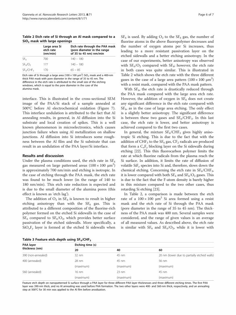
Table 2 Etch rate of Si through an Al mask compared to aSiO2 mask with large openings
Large area Sietch rate(nm/min)
Etch rate through the PAA mask(pore diameter in the rangeof 35 to 45 nm) nm/min
SF6 700 140 – 180
SF6/O2 177 140 – 180
SF6/CHF3 170 65 – 85
Etch rate of Si through a large area (100 × 100 μm2) SiO2 mask and a 400-nmthick PAA mask with pore diameter in the range of 35 to 45 nm. Thedifference in the etch rate is attributed to the small size of the etchingwindows, which is equal to the pore diameter in the case of thealumina mask.
Gianneta et al. Nanoscale Research Letters 2013, 8:71 Page 6 of 7http://www.nanoscalereslett.com/content/8/1/71
interface. This is illustrated in the cross-sectional SEMimage of the PAA/Si stack of a sample annealed at500°C before Al electrochemical oxidation (Figure 7).This interface undulation is attributed to the fact that Alannealing results, in general, in Al diffusion into the Sisubstrate and local creation of spikes. This is a wellknown phenomenon in microelectronics, which causesjunction failure when using Al metallization on shallowjunctions. Al diffusion into Si introduces some rough-ness between the Al film and the Si substrate that canresult in an undulation of the PAA layer/Si interface.
Results and discussionUnder the plasma conditions used, the etch rate in SF6gas measured on large patterned areas (100 × 100 μm2)is approximately 700 nm/min and etching is isotropic. Inthe case of etching through the PAA mask, the etch ratewas found to be much lower (in the range of 140 to180 nm/min). This etch rate reduction is expected andis due to the small diameter of the alumina pores (thiseffect is known as ‘etch lag’).The addition of O2 in SF6 is known to result in higher
etching anisotropy than with the SF6 gas. This isattributed to a different composition of the fluorine-richpolymer formed on the etched Si sidewalls in the case ofSF6 compared to SF6/O2, which provides better surfacepassivation of the etched sidewalls. More specifically, aSiOxFy layer is formed at the etched Si sidewalls when
Table 3 Feature etch depth using SF6/CHF3PAA layerthickness (nm)
Etching time (s)
20 40
390 (non-annealed) 32 nm 45
400 (annealed) 28 nm 45
(maximum) (m
560 (annealed) 16 nm 23
(maximum) (m
Feature etch depth on nanopatterned Si surface through a PAA layer for three diffelayer was 390-nm thick, and no Al annealing was used before PAA formation. The tstep at 500°C for 30 min was applied to the Al film before anodization.
SF6 is used. By adding O2 to the SF6 gas, the number offluorine atoms in the above fluoropolymer decreases andthe number of oxygen atoms per Si increases, thusleading to a more resistant passivation layer on theetched sidewalls and a better etching anisotropy. In thecase of our experiments, better anisotropy was observedwith SF6/O2 compared with SF6; however, the etch ratein both cases was quite similar. This is illustrated inTable 2 which shows the etch rate with the three differentgases in the case of a large area pattern (100 × 100 μm2)with a resist mask, compared with the PAA mask pattern.With SF6, the etch rate is drastically reduced through
the PAA mask compared with the large area etch rate.However, the addition of oxygen in SF6 does not createany significant difference in the etch rate compared withSF6, as in the case of large area etching. The only effectis a slightly better anisotropy. The significant differenceis between these two gases and SF6/CHF3. In this lastcase, the etch rate is lower, and better anisotropy isachieved compared to the first two cases.In general, the mixture SF6/CHF3 gives highly aniso-
tropic Si etching. This is due to the fact that with theaddition of CHF3 to the SF6 gas, CF2 radicals are producedthat form a CxFy blocking layer on the Si sidewalls duringetching [22]. This thin fluorocarbon polymer limits therate at which fluorine radicals from the plasma reach theSi surface. In addition, it limits the rate of diffusion ofvolatile SiFy species into Si and, therefore, slows down thechemical etching. Concerning the etch rate in SF6/CHF3,it is lower compared with both SF6 and SF6/O2 gases. Thisis due to the fact that the F-atom density is barely higherin this mixture compared to the two other cases, thusretarding Si etching [23].In Table 2, a comparison is made between the etch
rate of a 100 × 100 μm2 Si area formed using a resistmask and the etch rate of Si through the PAA mask(pore diameter in the range of 35 to 45 nm). The thick-ness of the PAA mask was 400 nm. Several samples wereconsidered, and the range of given values is an averageof all measured values. As described above, the etch rateis similar with SF6 and SF6/O2, while it is lower with
60
nm 20 nm (lower due to partially etched walls)
nm 56 nm
aximum) (maximum)
nm 45 nm
aximum) (maximum)
rent PAA layer thicknesses and three different etching times. The first PAAwo other layers were 400- and 560-nm thick, respectively, and an annealing

Gianneta et al. Nanoscale Research Letters 2013, 8:71 Page 7 of 7http://www.nanoscalereslett.com/content/8/1/71
SF6/CHF3. By increasing the PAA mask thickness from400 to 500 nm, the etch rate in SF6/CHF3 was reducedfrom approximately 70 to 50 nm/min.Table 3 shows the feature etch depth on nanopatterned Si
surface for the three different PAA layer thicknesses and thethree different etching times. The first PAA layer was 390-nmthick, and no Al annealing was used before PAA formation.The two other layers were 400- and 560-nm thick, respec-tively, and an annealing step at 500°C for 30 min was ap-plied to the Al film before anodization. We have observedthat although the annealing resulted in a better adhesionof the PAA layer on the Si surface (no detachment evenafter 60 s of etch time), it also created an undulation ofthe PAA/Si interface, which led to etching inhomogeneitieson the Si surface. In these two last cases, the etch depthvaried from zero (non-etched areas) to the maximum valueindicated in Table 3. In the case of the non-annealed sam-ple, the etch depth was homogeneous in the whole film.The problem was that for an etching time above 40 s, thelateral etching of the Si film underneath the mask led tomask detachment. The maximum etch depth achieved inthat case was around 45 nm.
ConclusionsWe investigated in detail the RIE of Si through a PAAmask for surface nanopatterning using SF6, SF6/O2, andSF6/CHF3 gases/gas mixtures. It was found that in allcases, the etch rate through the PAA mask was signifi-cantly lower than that on non-masked areas. Thesmallest etch rate and best anisotropic profiles wereobtained with the SF6/CHF3 gas mixture. Using a PAAmask with highly ordered hexagonally arranged nanopores,a perfect pattern transfer of the nanopores to a large Siarea is achieved. The same is possible on small pre-definedareas on the Si wafer.
Competing interestThe authors declare that they have no competing interests.
Authors’ contributionsVG performed the experiments of alumina formation and designed the cleanroom processes that were performed by the clean room operators. AOobtained the SEM images, and AGN supervised the work, drafted and editedthe paper. All authors read and approved the final manuscript.
Authors’ informationVG and AO are post-doctoral researchers. AGN is the director of research atNCSR Demokritos/IMEL and the head of the “Nanostructures forNanoelectronics, Photonics and Sensors” research group.
AcknowledgmentsThis work was partially financed by the 03ED375 PENED research projectwith funds from the Greek Ministry of Development (80%) and EU (20%).Funding was also received from the European Community's SeventhFramework Programme (FP7/2007-2013) under grant agreementNANOFUNCTION n°257375.
Received: 21 December 2012 Accepted: 4 February 2013Published: 12 February 2013
References1. Asoh H, Sasaki K, Ono S: Electrochemical etching of silicon through
anodic porous alumina. Electrochem Commun 2005, 7:953–956.2. Crouse D, Lo YH, Miller AE, Crouse M: Self-ordered pore structure of
anodized aluminum on silicon and pattern transfer. Appl Phys Lett 2000,76:49–51.
3. Zacharatos F, Gianneta V, Nassiopoulou AG: Highly ordered hexagonallyarranged nanostructures on silicon through a self-assembled silicon-integrated porous anodic alumina masking layer. Nanotechnology 2008,19:495306.
4. Zacharatos F, Gianneta V, Nassiopoulou AG: Highly ordered hexagonallyarranged sub-200 nm diameter vertical cylindrical pores on p-type Siusing non-lithographic pre-patterning of the Si substrate. Phys StatusSolidi A 2009, 206:1286–1289.
5. Hourdakis E, Nassiopoulou AG: High performance MIM capacitor usinganodic alumina dielectric. Microelectron Eng 2012, 90:12–14.
6. Hourdakis E, Nassiopoulou AG: High-density MIM capacitors with porousanodic alumina dielectric. IEEE Trans Electron Dev 2010, 57(10):2679–2683.
7. Huang GH, Lee EJ, Chang WJ, Wang NF, Hung CI, Houng MP: Chargetrapping behavior of SiO2-Anodic Al2O3–SiO2 gate dielectrics fornonvolatile memory applications. Solid State Electron 2009, 53:279–284.
8. Hourdakis E, Nassiopoulou AG: Charge-trapping MOS memory structureusing anodic alumina charging medium. Microelectron Eng 2011,88(7):1573–1575.
9. Masuda H, Fukuda K: Ordered metal nanohole arrays made by a two-stepreplication of honeycomb structures of anodic alumina. Science 1995,268:1466–1468.
10. Li AP, Birner A, Nielsch K, Gösele U: Hexagonal pore arrays with a50–420 nm interpore distance formed by self-organization in anodicalumina. J Appl Phys 1998, 84:6023–6026.
11. Lee W, Ji R, Gösele U: Fast fabrication of long-range ordered porousalumina membranes by hard anodization. Nat Mater 2006, 5:741–747.
12. Zhang F, Liu X, Pan C, Zhou J: Nano-porous anodic aluminium oxidemembranes with 6–19 nm pore diameters formed by a low-potentialanodizing process. Nanotechnology 2007, 18:345302.
13. Masuda H, Yamada H, Satoh M, Asoh H, Nakao M, Tamura T: Highlyordered nanochannel-array architecture in anodic alumina. Appl Phys Lett1997, 71(19):2770–2772.
14. Masuda H, Yasui K, Sakamoto Y, Nakao M, Tamamura T, Nishio K: Ideallyordered anodic porous alumina mask prepared by imprinting ofvacuum-evaporated Al on Si. Jpn J Appl Phys 2001, 40(11B):L1267–L1269.
15. Lei Y, Cai W, Wilde G: Highly ordered nanostructures with tunable size,shape and properties: a new way to surface nano-patterning using ultra-thin alumina masks. Progr Mater Sci 2007, 52:465–539.
16. Kokonou M, Gianakopoulos KP, Nassiopoulou AG: Few nanometer thickanodic porous alumina films on silicon with high density of verticalpores. Thin Solid Films 2007, 515:3602–3606.
17. Keller F, Hunter MS, Robinson DL: Structural features of oxide coatings onaluminum. J Electrochem Soc 1963, 100:411–419.
18. Kokonou M, Nassiopoulou AG: Nanostructuring Si surface and Si/SiO2
interface using porous-alumina-on-Si template technology. Electricalcharacterization of Si/SiO2 interface. Physica E 2007, 38:1–5.
19. Asoh H, Matsuo M, Yoshihama M, Ono S: Transfer of nanoporous pattern ofanodic porous alumina into Si substrate. Appl Phys Lett 2003, 83:4408–4410.
20. Sai H, Fujii H, Arafune K, Ohshita Y, Yamaguchi M: Antireflectivesubwavelength structures on crystalline Si fabricated using directly formedanodic porous alumina masks. Appl Phys Lett 2006, 88:201116–201118.
21. Lu CC, Huang YS, Huang JW, Chang CK, Wu SP: A macroporous TiO2
oxygen sensor fabricated using anodic aluminium oxide as an etchingmask. Sensors 2010, 10:670–683.
22. Gogolides E, Grigoropoulos S, Nassiopoulou AG: Highly anisotropic room-temperature sub-half-micron Si reactive ion etching using fluorine onlycontaining gases. Microelectron Eng 1995, 27:449–452.
23. Jansen H, Gardeniers H, Boer M, Elwenspoek M, Fluitman J: A survey on thereactive ion etching of silicon in microtechnology. J Micromech Microeng1995, 6:14–28.
doi:10.1186/1556-276X-8-71Cite this article as: Gianneta et al.: Si nanopatterning by reactive ionetching through an on-chip self-assembled porous anodic aluminamask. Nanoscale Research Letters 2013 8:71.
Related Documents