Welcome message from author
This document is posted to help you gain knowledge. Please leave a comment to let me know what you think about it! Share it to your friends and learn new things together.
Transcript
Embedded Systems
Firmware Demystified
Ed Sutter
CMP Books Lawrence, Kansas 66046 CMP Books CMP Media LLC 1601 West 23rd Street, Suite 200 Lawrence, Kansas 66046
USA www.cmpbooks.com
Designations used by companies to distinguish their products are often claimed as trademarks.
In all instances where CMP Books is aware of a trademark claim, the product name appears
in initial capital letters, in all capital letters, or in accordance with the vendor’s capitalization preference. Readers should contact the appropriate companies for more
complete information on trademarks and trademark registrations. All trademarks and
registered trademarks in this book are the property of their respective holders.
Copyright © 2002 by Lucent Technologies, except where noted otherwise. Published by CMP
Books, CMP Media LLC. All rights reserved. Printed in the United States of America. No part
of this publication may be reproduced or distributed in any form or by any means, or stored
in a database or retrieval system, without the prior written permission of the publisher.
The programs in this book are presented for instructional value. The programs have been
carefully tested, but are not guaranteed for any particular purpose. The publisher does
not offer any warranties and does not guarantee the accuracy, adequacy, or completeness
of any information herein and is not responsible for any errors or omissions. The publisher
assumes no liability for damages resulting from the use of the information in this book
or for any infringement of the intellectual property rights of third parties that would
result from the use of this information.
Acquisition Editor: Robert Ward
Editors: Joe Casad and Catherine Janzen
Layout production: James Hoyt, Justin Fulmer, and Madeleine Reardon Dimond
Managing Editor: Michelle O’Neal Cover art: Rupert Adley (www.solidimages.com)
Cover design: Damien Castaneda
Distributed in the U.S. and Canada by: Publishers Group West 1700 Fourth Street Berkeley, CA 94710
1-800-788-3123 www.pgw.com
ISBN: 1-57820-099-7
Table of Contents
Preface . . . . . . . . . . . .
. . . . . . . . . . . . . .
. . . . . . . . . . . . . . . . .
vii
Who Is the
Reader? . . . . . . . . . . .
. . . . . . . . . . . . .
. . . . . . . . . . . . .
. . . . . . . . . . ix
What’s Covered in this
Book? . . . . . . . . . .
. . . . . . . . . . . . .
. . . . . . . . . . . . . . . .
ix
Conventions . . . . . . .
. . . . . . . . . . . . .
. . . . . . . . . . . . .
. . . . . . . . . . . . .
. . . . . . . xii
Source
Code . . . . . . . . . .
. . . . . . . . . . . . .
. . . . . . . . . . . . .
. . . . . . . . . . . . . . . . .
xii
Acknowledgments . . . . .
. . . . . . . . . . . . .
. . . . . . . . . . . . .
. . . . . . . . . . . . . . . . .
xii
Chapter 1 A Hard
Start . . . . . . . . . . . .
. . . . . . . . . . . . . . . . . .
1
System
Requirements . . . . . . . . . .
. . . . . . . . . . . . .
. . . . . . . . . . . . .
. . . . . . . . . . . 2
Central Processing
Unit . . . . . . . . . .
. . . . . . . . . . . . .
. . . . . . . . . . . . .
. . . . . . . . . 3
System
Memory . . . . . . . . .
. . . . . . . . . . . . .
. . . . . . . . . . . . .
. . . . . . . . . . . . . . .
10
CPU
Supervision . . . . . . .
. . . . . . . . . . . . .
. . . . . . . . . . . . .
. . . . . . . . . . . . . . . .
12
Serial Port
Drivers . . . . . . . . .
. . . . . . . . . . . . .
. . . . . . . . . . . . .
. . . . . . . . . . . . . 15
Ethernet
Interface . . . . . . . .
. . . . . . . . . . . . .
. . . . . . . . . . . . .
. . . . . . . . . . . . . . .
17
Flash Device
Options . . . . . . . . .
. . . . . . . . . . . . .
. . . . . . . . . . . . .
. . . . . . . . . . . 18
The CPU/Memory
Interface . . . . . . . .
. . . . . . . . . . . . .
. . . . . . . . . . . . .
. . . . . . . 19
Summary . . . . . . . . .
. . . . . . . . . . . . .
. . . . . . . . . . . . .
. . . . . . . . . . . . .
. . . . . . . 27
Chapter 2 Getting
Started . . . . . . . . . . . .
. . . . . . . . . . . . . . .
29
How Is It Done on a
PC? . . . . . . . . . . . .
. . . . . . . . . . . . .
. . . . . . . . . . . . . . . . . .
30
Building
Libraries . . . . . . . .
. . . . . . . . . . . . .
. . . . . . . . . . . . .
. . . . . . . . . . . . . . .
45
Up
Front . . . . . . . . . .
. . . . . . . . . . . . .
. . . . . . . . . . . . .
. . . . . . . . . . . . .
. . . . . . 47
Run
Time . . . . . . . . . .
. . . . . . . . . . . . .
. . . . . . . . . . . . .
. . . . . . . . . . . . .
. . . . . . 55
Hardware Sanity Tests for
the Firmware
Developer . . . . . . . .
. . . . . . . . . . . . . . .
55
Summary . . . . . . . . .
. . . . . . . . . . . . .
. . . . . . . . . . . . .
. . . . . . . . . . . . .
. . . . . . . 60
Chapter 3 Introducing
MicroMonitor. . . . . . . . . . .
. . . . . . . . 61
An Embedded System Boot
Platform . . . . . . . . . . .
. . . . . . . . . . . . .
. . . . . . . . . . 61
Chapter 4 Assembly
Required . . . . . . . . . . . .
. . . . . . . . . . . . 69
Just After
Reset . . . . . . . . . . . .
. . . . . . . . . . . . .
. . . . . . . . . . . . .
. . . . . . . . . . . . 70
I/O
Initialization . . . . . .
. . . . . . . . . . . . .
. . . . . . . . . . . . .
. . . . . . . . . . . . .
. . . . . 76
Establish Exception
Handlers . . . . . . . .
. . . . . . . . . . . . .
. . . . . . . . . . . . .
. . . . . . 76
Summary . . . . . . . . .
. . . . . . . . . . . . .
. . . . . . . . . . . . .
. . . . . . . . . . . . .
. . . . . . . 86
Chapter 5 Command Line
Interface. . . . . . . . . . . .
. . . . . . . . .87
CLI
Features . . . . . . . . . . .
. . . . . . . . . . . . .
. . . . . . . . . . . . .
. . . . . . . . . . . . . . .
88
CLI Data Structure and the
Command
Table . . . . . . . . . .
. . . . . . . . . . . . . . . . .
89
CLI
Processing . . . . . . .
. . . . . . . . . . . . .
. . . . . . . . . . . . .
. . . . . . . . . . . . . . . . .
90
The Functions Beneath the
Command
Name . . . . . . . . . .
. . . . . . . . . . . . . . . . .
91
Shell Variable and Symbol
Processing . . . . . . . .
. . . . . . . . . . . . .
. . . . . . . . . . . . 96
Command-Line
Redirection . . . . . . .
. . . . . . . . . . . . .
. . . . . . . . . . . . .
. . . . . . . 99
Command Line Editing and
History . . . . . . . . .
. . . . . . . . . . . . .
. . . . . . . . . . . 105
User
Levels . . . . . . . . .
. . . . . . . . . . . . .
. . . . . . . . . . . . .
. . . . . . . . . . . . . . . . .
111
Password
Protection . . . . . . .
. . . . . . . . . . . . .
. . . . . . . . . . . . .
. . . . . . . . . . . . 115
Summary . . . . . . . . .
. . . . . . . . . . . . .
. . . . . . . . . . . . .
. . . . . . . . . . . . .
. . . . . 116
Chapter 6 Interfacing to Flash
Memory . . . . . . . . . . . .
. . . .117
The Interface
Functions . . . . . . . . . . .
. . . . . . . . . . . . .
. . . . . . . . . . . . .
. . . . . 118
Flash Driver Front
End . . . . . . . . . . .
. . . . . . . . . . . . .
. . . . . . . . . . . . .
. . . . . . 132
Summary . . . . . . . . .
. . . . . . . . . . . . .
. . . . . . . . . . . . .
. . . . . . . . . . . . .
. . . . . 136
Chapter 7 A Flash File
System. . . . . . . . . . . . .
. . . . . . . . . . .137
The Role of TFS in the
Platform . . . . . . . . . . .
. . . . . . . . . . . . .
. . . . . . . . . . . . 138
The TFS Design
Criteria . . . . . . . .
. . . . . . . . . . . . .
. . . . . . . . . . . . .
. . . . . . . . 138
File
Attributes . . . . . . . .
. . . . . . . . . . . . .
. . . . . . . . . . . . .
. . . . . . . . . . . . . . . .
139
High-Level
Details . . . . . . . . .
. . . . . . . . . . . . .
. . . . . . . . . . . . .
. . . . . . . . . . . 141
Flash Space Overhead
Required by
TFS . . . . . . . . . . .
. . . . . . . . . . . . .
. . . . . . 143
Defragmentation . . . . .
. . . . . . . . . . . . .
. . . . . . . . . . . . .
. . . . . . . . . . . . . . . . .
144
TFS
Implementation . . . . .
. . . . . . . . . . . . .
. . . . . . . . . . . . .
. . . . . . . . . . . . . .
146
Adding and Deleting
Files . . . . . . . . . .
. . . . . . . . . . . . .
. . . . . . . . . . . . . . . . . .
155
To Load or Not to
Load . . . . . . . . . . .
. . . . . . . . . . . . .
. . . . . . . . . . . . .
. . . . . 165
File
Decompression . . . . . .
. . . . . . . . . . . . .
. . . . . . . . . . . . .
. . . . . . . . . . . . . .
170
Execute In
Place . . . . . . . . . .
. . . . . . . . . . . . .
. . . . . . . . . . . . .
. . . . . . . . . . . . 171
Summary . . . . . . . . .
. . . . . . . . . . . . .
. . . . . . . . . . . . .
. . . . . . . . . . . . .
. . . . . 172
Chapter 8 Executing
Scripts . . . . . . . . . . . .
. . . . . . . . . . . . .173
The Script
Runner . . . . . . . . . . .
. . . . . . . . . . . . .
. . . . . . . . . . . . .
. . . . . . . . . 173
Conditional
Branching . . . . . . . .
. . . . . . . . . . . . .
. . . . . . . . . . . . .
. . . . . . . . . 181
A Few
Examples . . . . . . . . .
. . . . . . . . . . . . .
. . . . . . . . . . . . .
. . . . . . . . . . . . . 187
Summary . . . . . . . . .
. . . . . . . . . . . . .
. . . . . . . . . . . . .
. . . . . . . . . . . . .
. . . . . 191
Chapter 9Network
Connectivity . . . . . . . . . . .
. . . . . . . . . . .193
Ethernet . . . . . . . . . . .
. . . . . . . . . . . . .
. . . . . . . . . . . . .
. . . . . . . . . . . . . . . . .
194
ARP . . . . . . . . . . .
. . . . . . . . . . . . .
. . . . . . . . . . . . .
. . . . . . . . . . . . .
. . . . . . . 194
IP . . . . . . . . . . . .
. . . . . . . . . . . . .
. . . . . . . . . . . . .
. . . . . . . . . . . . .
. . . . . . . . . 195
ICMP . . . . . . . . . . .
. . . . . . . . . . . . .
. . . . . . . . . . . . .
. . . . . . . . . . . . .
. . . . . . . 196
UDP and
TCP . . . . . . . . . . .
. . . . . . . . . . . . .
. . . . . . . . . . . . .
. . . . . . . . . . . . . 197
DHCP/BOOTP . . . . . . . .
. . . . . . . . . . . . .
. . . . . . . . . . . . .
. . . . . . . . . . . . . . . .
198
Applied to Embedded
Systems . . . . . . . . .
. . . . . . . . . . . . .
. . . . . . . . . . . . . . . .
199
Summary . . . . . . . . .
. . . . . . . . . . . . .
. . . . . . . . . . . . .

. . . . . . . . . . . . .
. . . . . . 209
Chapter 10 File/Data
Transfer . . . . . . . . . . . .
. . . . . . . . . . . 211
Xmodem . . . . . . . . . . . . . . . . . . . . . . . . . . . . . . . . . .
. . . . . . . . . . . . . . . . . . . . 211
TFTP . . . . . . . . . . . . . . . . . . . . . . . . . . . . . . . . . . .
. . . . . . . . . . . . . . . . . . . . . . 219
Field Upgrade
Capability . . . . . . . . . . . . . . . . . . . . . . . . . . . . . . . . . . . . . . . . . .
230
Summary . . . . . . . . . . . . . . . . . . . . . . . . . . . . . . . . .
. . . . . . . . . . . . . . . . . . . . . 231
Chapter 11 Adding the Application . . . . . . . . . . . . . . . . . . . 233
Different Memory
Map . . . . . . . . . . . . . . . . . . . . . . . . . . . . . . . . . . . . . . . . . . .
233
Less Intense
Startup . . . . . . . . . . . . . . . . . . . . . . . . . . . . . . . . .
. . . . . . . . . . . . . 234
Establishing an Application
Stack . . . . . . . . . . . . . . . . . . . . . . . . . . . . . . . . . . .
235
Connecting to the Monitor’s API . . . . . . . . . . . . . . . . . . . . . . . . . . . . . . . . . . . .
235
The Application start()
Function . . . . . . . . . . . . . . . . . . . . . . . . . . . . . . . . . .
240
The Application main()
Function . . . . . . . . . . . . . . . . . . . . . . . . . . . . . . . . . . .
241
Application-Originated
Drivers . . . . . . . . . . . . . . . . . . . . . . . . . . . . . . . . . . . . .
242
Application-Based CLI Uses Monitor
CLI . . . . . . . . . . . . . . . . . . . . . . . . . . . . . 242
Scripts Run Through the Application’s CLI . . . . . . . . . . . . . . . . . . . . . . . . . . . . 244
Summary . . . . . . . . . . . . . . . . . . . . . . . . . . . . . . . . .
. . . . . . . . . . . . . . . . . . . . . 245
Chapter 12 Monitor-Based Debugging . . . . . . . . . . . . . . . . 247
Different Type of Debug
Philosophy . . . . . . . . . . . . . . . . . . . . . . . . . . . . . . . . .
248
Breakpoints . . . . . . . . . . . . . . . . . . . . . . . . . . . . . . .
. . . . . . . . . . . . . . . . . . . . . 249
Adding Symbolic
Capabilities . . . . . . . . . . . . . . . . . . . . . . . . . . . . . . . . . . . . . . .
254
Displaying
Memory . . . . . . . . . . . . . . . . . . . . . . . . . . . . . . . . . . . . . . . . . . . . . .
255
Overlaying a C Structure onto
Memory . . . . . . . . . . . . . . . . . . . . . . . . . . . . . . . 261
Stack
Trace . . . . . . . . . . . . . . . . . . . . . . . . . . . . . . . . . .
. . . . . . . . . . . . . . . . . . 277
Testing for Stack
Overflow . . . . . . . . . . . . . . . . . . . . . . . . . . . . . . . . . . . . . . . .
283
System
Profiling . . . . . . . . . . . . . . . . . . . . . . . . . . . . . . . .
. . . . . . . . . . . . . . . . . 289
Summary . . . . . . . . . . . . . . . . . . . . . . . . . . . . . . . . .
. . . . . . . . . . . . . . . . . . . . . 299
Chapter 13 Porting MicroMonitor to the
ColdFire™ MCF5272 . . . . . . . . . . . . . . . . . . . . . . . . . . .
301
Source Code Directory
Tree . . . . . . . . . . . . . . . . . . . . . . . . . . . . . . . . . . . . . . . .
302
The
Makefile . . . . . . . . . . . . . . . . . . . . . . . . . . . . . . . .
. . . . . . . . . . . . . . . . . . . 304
The Configuration Header
File . . . . . . . . . . . . . . . . . . . . . . . . . . . . . . . . . . . . .
313
Stepping Through the
Port . . . . . . . . . . . . . . . . . . . . . . . . . . . . . . . . . . . . . . . .
319
Summary . . . . . . . . . . . . . . . . . . . . . . . . . . . . . . . . .
. . . . . . . . . . . . . . . . . . . . 332
Conclusion . . . . . . . . . . . . . . . . . . . . . . . . . . . .
. . . . . . . . . . . .335
Appendix A Building a Host-Based Toolbox . . . . . . . . . . .337
Interfacing to Files on the
Host . . . . . . . . . . . . . . . . . . . . . . . . . . . . . . . . . . . . .
338
Interfacing to the PC Serial
Port . . . . . . . . . . . . . . . . . . . . . . . . . . . . . . . . . . . .
342
PC-Based UDP Transactions: moncmd. . . . . . . . . . . . . . . . . . . . . . . . . . . . . . . . 344
Summary . . . . . . . . . . . . . . . . . . . . . . . . . . . . . . . . .
. . . . . . . . . . . . . . . . . . . . 348
Appendix B RTOS Overview. . . . . . . . . . . . . . . . . . . . . . . .349
The
Scheduler . . . . . . . . . . . . . . . . . . . . . . . . . . . . . . . .
. . . . . . . . . . . . . . . . . . 350
Tasks, Threads, and
Processes . . . . . . . . . . . . . . . . . . . . . . . . . . . . . . . . . . . . .
351
Preemption, Time Slicing, and
Interrupts . . . . . . . . . . . . . . . . . . . . . . . . . . . . . 352
Semaphores, Events, Messages, and
Timers . . . . . . . . . . . . . . . . . . . . . . . . . . . 353
Reentrancy . . . . . . . . . . . . . . . . . . . . . . . . . . . . . . .
. . . . . . . . . . . . . . . . . . . . . 356
Good Concurrency vs. Bad
Concurrency . . . . . . . . . . . . . . . . . . . . . . . . . . . . . 357
Summary . . . . . . . . . . . . . . . . . . . . . . . . . . . . . . . . .
. . . . . . . . . . . . . . . . . . . . 358
Index . . . . . . . . . . . . . . . . . . . . . . . . . . . . . .
. . . . . . . . . . . . . . .359
What’s on the CD-ROM? . . . . . . . . . . . . . . . . . . . . . . . . . . . . .372
Preface
An embedded system is just a computer buried inside some other product. Surpris-
ingly, you can know a great deal about programming and computing and still get
lost in the arcane world of embedded systems. In the world of embedded systems
programming, countless details — both hardware- and software-related — make
the development process seem like a path that few have traveled and even fewer
have survived. How do software, hardware, and firmware differ? How in the world does a 100,000-line program end up inside a device smaller than my fingernail? What is flash memory and why do I need a cache? What is the difference between a task and a process? Do I need to worry about reentrancy? As we progress through
Embedded Systems Firmware Demystified, you will come to see that these questions are not as complex as they first appear.
Embedded systems programming spans a wide range of activities from building
programmable logic at the most concrete end to writing a UNIX™ process at the
most abstract end. Bracketed by these poles, the industry has exploded in the
last 20 years. In the late seventies, assemblers were considered luxuries. A
typical embedded system used less than 64Kb of system memory (bits, not bytes!).
There was no hardware hand-off to the firmware developer. The same person that drew the schematics and soldered the prototype also wrote the firmware that pulled the whole thing together. By the time Intel introduced the 8085 chip,
it was clear that those pesky microprocessors were here to stay. In the eighties,
the Motorola versus Intel CPU wars started, and C became a popular choice for
the elite few who dared to mess with a high-level language and an EPROM
programmer. Today, microprocessors are everywhere and range from the 4- and
8-bit workhorses still dominating the industry to 1GHz 64-bit processors that
almost need a freezer (microprocessor-controlled, no doubt) to keep them cool.
Over the years, the complexity of these systems has snowballed. The industry
has transitioned from programming a DEC PDP machine with binary codes on the front
panel to applying object-oriented design to a microcontroller in a toaster. If you
let the trend get to you, the changes can seem frazzling. There are microprocessors
and microcontrollers; RAM, DRAM, and SDRAM; pipelining and superscalar; EPROM and
flash memory; RISC and CISC; and RAS and CAS and cache — and that’s just the beginning.
Now, everything from toothbrushes (no kidding) to fighter jets are likely to have a version controlled by a microprocessor of some kind. With this trend come tools
and technologies. One can easily be overwhelmed by the available choices in hardware
(integrated circuits that the firmware must make work) and software (tools that are used to build the firmware application).
The goal of this book is to prepare you for a real embedded systems project by
walking you through an entire embedded systems design. Not coincidentally, the
project source code included is a piece of firmware — an embedded boot platform
— that can simplify all your future projects. I assume a small hardware design
with CPU, memory, and some peripherals. I present a basic schematic and walk you
through the method in which instructions are fetched from memory. I discuss devices,
as well as concepts. I examine flash memory versus EPROM, SRAM versus DRAM, microcontroller versus microprocessor, and data bus versus address bus. I also
explain how you convert your C and assembly language source code to a binary image
that ends up in the memory device from which the CPU boots (the boot flash memory). Several chapters cover the basic steps of starting up an embedded system and
getting a working application (including the basic boot in assembler), exception
handling, flash memory drivers, a flash file system, and serial and Ethernet connections. The result is an understanding of how an embedded systems project gets
started and how to build a platform on which an embedded systems application can
reside.
Sound exciting? Great! Sound scary? It’s not! The intent of this book is not to discuss the latest superscalar architecture or the antenna effects of copper routes
on a printed circuit board, nor does it present a high-level abstract design process.
(Advanced architectures and transmission-line effects are certainly important, but
they are not the topic of this book.) This book is for those who want to get their
hands dirty without being overwhelmed by industry jargon or design-specific techni-cal details. By the end of this book, you will know how to read a basic schematic,
know what goes into the boot flash device, and understand the major components of a complete embedded systems development platform.
Who Is the Reader?
At the minimum, I assume the reader has some experience with C and basic assembly
language concepts. I do not assume any electronics or hardware background. Thus,
readers with a wide range of programming backgrounds will find this book useful.
Computer science or electrical engineering students without a significant background in firmware development, but at least an interest, can obviously benefit from this book.
Low-level firmware developers will find the working example helpful, as it includes documentation and code explanations for an extensible firmware development platform. I explain the details associated with booting new
hardware and the way in which the CPU interacts with peripherals. Topics range
from the lowest-level boot to a Trivial File Transfer Protocol (TFTP)
implementation over Ethernet. You can port the code in this book to your own
target system or integrate snippets of this code with your existing firmware platform.
Hardware developers will find the completed platform useful for helping analyze and debug hardware beyond the CPU complex. For those inquisitive enough to step
away from hardware to learn more about the firmware process, this book provides a way to get started without getting too far from the hardware. (Hardware
designers regularly make the transition to programming in the firmware/software world.)
Project leaders will also find this book useful, as the firmware package presented is a mature platform. The platform is applicable to a wide range of real-time
operating systems (RTOS) and target architectures, and it is extremely easy
to port to new systems. The fact that the platform is fairly target- and
RTOS-independent makes the transition to a different target or RTOS much less
painful.
What’s Covered in this Book? Chapter 1: A Hard Start describes a basic CPU structure, with support
peripherals, on which the firmware discussed in this book can execute. The design includes, among other things, a core microprocessor, RAM, flash memory, serial I/O, and CPU supervision. Each element of the design is discussed (for example,
CPU supervision and types of volatile and non-volatile memory devices). This
chapter also examines the basics of how microprocessors fetch instructions from
the memory device and how cache makes these fetches more efficient. The chapter covers the typical peripherals found in many microprocessors today, without
being specific to a particular device. Chapter 2: Getting Started introduces the writing and building of programs for embedded devices. This chapter explains the differences between a
native-compila-tion and a cross-compilation environment. I discuss file formats and break down the task of burning the boot flash memory into simple steps. I also explain
the importance of the link editor file and show how it is used to allocate sections of the application code to portions of the target memory. The chapter also discusses
some preliminary tests and preparations you must undertake before you start program-
ming the firmware.
Chapter 3:Introducing MicroMonitor introduces the boot platform, or boot monitor, used in embedded systems. This monitor, called MicroMonitor, has a full list of
features and serves as a learning tool to teach you about the firmware development process.
Chapter 4: Assembly Required describes MicroMonitor’s reset vector, or startup code. I then build some serial drivers and discuss an implementation for establishing
exception handlers.
Chapter 5:Command Line Interface describes how to build a shell around the core functionality introduced in Chapter 4. I start with the command line interface
(CLI).Next, I explain the processing that parses the input command line and that
eventually (through the table of structures) calls a function corresponding to the
command line. The command line interface includes shell variables and symbols,
command line editing and history, user levels, and password protection.
Chapter 6:Interfacing to Flash Memory is the first of three chapters dealing prima-rily with flash memory. I describe a sample platform with (potentially several) banks of flash memory. This chapter discusses the lowest-level details involved in programming flash memory and presents a useful approach for target hardware with different flash memory configurations.
Chapter 7:A Flash File System discusses the creation of a tiny file system (TFS) which resides in flash memory. This simple file system is offered as an alternative to some of the more complicated approaches taken by many flash file system designers. I also describe some of the advantages and disadvantages of the trade-offs made
in the design of TFS.
Chapter 8: Executing Scripts describes a feature that, with a CLI for command exe-cution and a TFS for file storage, lets a file execute as a script or small program. This chapter examines the surprisingly simple details that combine the CLI and TFS
to create a simple interpreter. The CLI commands are chosen to provide the CLI/TFS
user with a simple but useful programming environment. Conditional branching and
subroutines are just a few of the capabilities of this system.
Chapter 9: Network Connectivity examines the elements needed to connect as a node on a network. Just as flash memory is becoming a standard boot memory device, so too is Ethernet becoming a standard interface on many embedded systems. This chapter
discusses several protocols used with embedded systems, including Ethernet, ARP,
ICMP, IP, UDP, and BOOTP/DHCP. Finally, the chapter examines encapsulation of
network layers — one on top of another — by small blocks of code that know only
about their own piece of the packet payload.
Chapter 10: File/Data Transfer discusses two common file-transfer protocols: Xmo-dem for serial interfaces and TFTP for networks. Here I explain each of these proto-
cols as implemented in the boot monitor package. The Xmodem and TFTP implementations
presented in this book can transfer files and raw memory both to and from the target.
Chapter 11: Adding the Application shows you how the platform provides the base on which applications reside. The example in this chapter is a simple application
with no RTOS, but it is clear that this platform supports just about any environment.
You, as the developer, decide how much of the platform remains accessible by the
application after the application takes over the system. This chapter discusses
how the application is built to reside within the TFS and how the platform’s loader automatically transfers the file from flash memory space to RAM space for execution.
Chapter 12:Monitor-Based Debugging discusses some of the monitor’s on-board debugging capabilities and shows the implementation of these capabilities because,
whether you want to admit it or not, you’re going to have to debug your code. Here you’ll learn how to create a basic symbolic debugger that can display memory as a structure (instead of as raw data), set breakpoints, single-step through a program,
profile a program’s execution, and dump a stack trace. The debugging techniques described in this chapter do not require in-chip support or an external debugger.
Chapter 13:Porting MicroMonitor to the ColdFire™ MCF5272 explains the process of porting the MicroMonitor firmware package to a Motorola MCF5272 (ColdFire)
evaluation board. The text introduces the directory structure of the source code
on the CD and walks through the monitor-specific details of the porting process. This chapter completes the process begun in earlier chapters.
Appendix A:Building a Host-Based Toolbox provides snippets of code that might prove useful for interfacing to files, serial ports, and sockets. Despite the fact that this book is about firmware, you are likely to have to do some native programming eventually. Even if you’ve already done a lot of native programming, the code presented here should speed your work.
Appendix B: RTOS Overview introduces some of the basic concepts of a real-time operating system (RTOS), which lets you expand your environment from supporting
single-threaded programs to multi-threaded ones. Several books are available
on this subject, so this appendix is not intended as an exhaustive study. I,
however, present a fundamental explanation of what multi-tasking can do for
you and why preemption is a beautiful yet dangerous feature.
Conventions
Throughout the book, I use different typefaces to differentiate between a) the
book’s regular text and b) special software tools, code, and so forth. General text is in roman font. Terms used for the first time are in italic. A monospaced font indicates code, software tools, hexadecimal numbers, filenames, data types, variables, and other identifiers, as well as other special items.
Source Code
This book covers a lot of source code. When the text describes various portions
of the code in detail, snippets or entire functions are included. All code in
this text has been transferred from the original working C source code and is
included on the CD. Some implementation details that were not applicable to
the discussion were removed from the text listings to make the presentation
clearer. I have made every effort to maintain accuracy between the original
code and the code presented in the text; however, the code on the CD is the
complete working version. If you have questions, please refer to the code on
the CD.
Acknowledgments
I want to thank my good friends and managers at Lucent — Roger Levy and Paul
Wilford — for their support and encouragement. Also, much thanks to my good
friends Patricia Dunkin and Agesino Primatic, Jr. for reviewing the text and
providing a lot of good comments and suggestions.
My appreciation goes to the team at CMP Books. Thanks to Joe Casad, Catherine
Janzen, and Robert Ward for editorial and technical contributions (special
thanks to Robert for dealing with my many questions and paranoias throughout
this whole process). Thanks to Michelle O’Neal, Justin Fulmer, James Hoyt, and Madeleine Reardon Dimond for typesetting, illustrating, and indexing the book.
Finally, I want to thank my wife, Lucy, for her endless encouragement through
this project. I also want to thank my son, Tommy, for helping me keep my
priorities in line. Most of all, I want to thank my Lord and Savior, Jesus Christ,
for the sacrifice that He made to provide me with eternal salvation. It just doesn’t get any better than that!
1
Chapter 1
A Hard Start
Although the primary focus of this book is firmware development, a good firmware developer must have a reasonable understanding of the hardware on which the
firmware resides. You could compare a firmware programmer to someone who changes oil at a gas station: if all that person knows is how to perform an oil change,
he won’t have the skills to notice warning signs that a fully trained mechanic would pick up right away. A narrowly trained technician may change the oil
competently but not notice other problems like a leaky head gasket. Sooner or
later something else will go wrong, remain unnoticed, and cause additional
trouble due to the techni-cian’s limited knowledge. This chapter explains what a firmware engineer needs to know about the hard-
ware in a typical system. The goal is not to turn you into a hardware designer
but simply to explain enough so that you can do more than “change the oil.” To achieve this goal, this chapter discusses some of the common CPU support
peripherals and examines how the hardware processor does its job. I will start
by focusing in on the type of system that this book addresses.You will learn
about some of the most common features of today’s microprocessor-based systems, some of which reside within the CPU silicon itself and others which are usually
external to the CPU. I will also discuss the sequence of steps that the CPU
takes to retrieve an instruction and the advantages and snags that are
introduced by the use of cache.
At the end of this chapter (although you will still not be a qualified hardware designer) you will hopefully have a better understanding of the hardware
platform onto which you will be installing your firmware.
System Requirements
The hardware required for an embedded system varies greatly depending on its
intended use. Some tiny systems have barely 1K data space and 16K of instruction
space, while high-performance systems might run a 1GHz 64-bit processing engine
with 32MB CompactFlash and 128MB DRAM. In this book, I focus mostly on systems
with capabilities that fall somewhere in the middle. The firmware I’ll discuss does require some memory space (ranging from 32K to 256K of flash memory and 8K to 128K of RAM) depending on what capabilities are built in, so it is not
appropriate for small microcontroller (8051, 68HC05/11/12, etc.) projects. On
the other hand, this code doesn’t need (or want!) a large machine to work successfully.
Figure 1.1 represents a complete system. Using this system model, you
canprogram your own devices, talk to the PC, and even serve HTML pages to a
network browser. If you need to skimp, you can eliminate the reset/watchdog
and battery-backed-RAM/time-of-day (BBRAM/TOD) clock controller and still have
the capabilities I listed! I include these capabilities in our model because
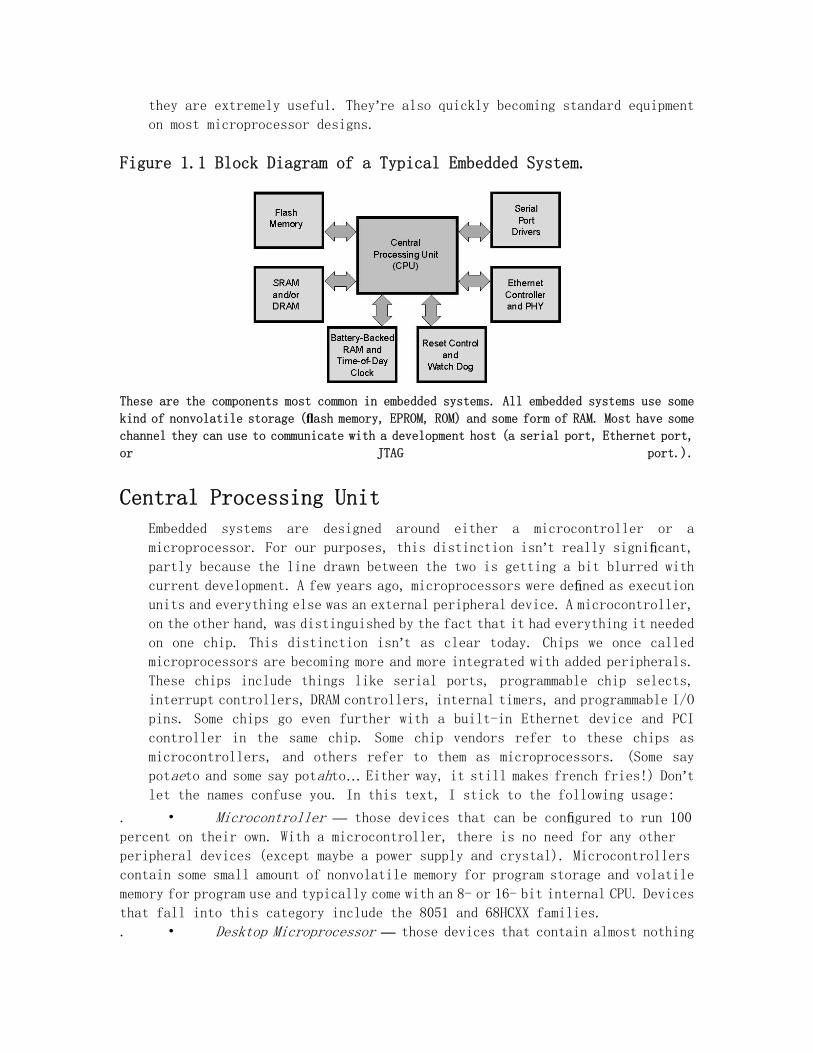
they are extremely useful. They’re also quickly becoming standard equipment on most microprocessor designs.
Figure 1.1 Block Diagram of a Typical Embedded System.
These are the components most common in embedded systems. All embedded systems use some
kind of nonvolatile storage (flash memory, EPROM, ROM) and some form of RAM. Most have some channel they can use to communicate with a development host (a serial port, Ethernet port,
or JTAG port.).
Central Processing Unit
Embedded systems are designed around either a microcontroller or a
microprocessor. For our purposes, this distinction isn’t really significant, partly because the line drawn between the two is getting a bit blurred with
current development. A few years ago, microprocessors were defined as execution units and everything else was an external peripheral device. A microcontroller,
on the other hand, was distinguished by the fact that it had everything it needed
on one chip. This distinction isn’t as clear today. Chips we once called microprocessors are becoming more and more integrated with added peripherals.
These chips include things like serial ports, programmable chip selects,
interrupt controllers, DRAM controllers, internal timers, and programmable I/O
pins. Some chips go even further with a built-in Ethernet device and PCI
controller in the same chip. Some chip vendors refer to these chips as
microcontrollers, and others refer to them as microprocessors. (Some say
potaeto and some say potahto… Either way, it still makes french fries!) Don’t let the names confuse you. In this text, I stick to the following usage:
. • Microcontroller — those devices that can be configured to run 100 percent on their own. With a microcontroller, there is no need for any other
peripheral devices (except maybe a power supply and crystal). Microcontrollers
contain some small amount of nonvolatile memory for program storage and volatile
memory for program use and typically come with an 8- or 16- bit internal CPU. Devices
that fall into this category include the 8051 and 68HCXX families.
. • Desktop Microprocessor — those devices that contain almost nothing
except the processing engine. They immediately require complex support chips as
their peripherals. The low end of these devices are 32-bit chips, but 64- and 128-
bit processors are getting more and more common. This category includes devices
like the K6, Pentium, and G4 processors.
. • Embedded Microprocessor — those devices that contain a processing
unit and some set of peripherals typically seen in an embedded system. These devices
generally fall in the 16- and 32- bit category and include processors like the 68332,
PPC860, and SH2.
. • CPU (Central Processing Unit) — this term can refer to any of the
above, or it can refer to just the processing section of a microcontroller or
embedded microprocessor.
Keep in mind that these definitions are not the rule in the industry. You should also note that there is some overlap between the different terms. Both
microcontrollers and desktop microprocessors are used in embedded systems. In
fact, back in the 1980s, microcontrollers were even used in some of the first desktop machines.
Microcontrollers, as defined above, dominate the embedded systems market by several orders of magnitude. However, silicon (both processor and memory) prices
are dropping, and the larger 16- and 32-bit processors are gaining ground in embed-
ded applications. This book generally focuses on systems based on embedded micro-
processors.
Embedded microprocessors come in a variety of shapes and sizes. They are even
becoming available as logic cores designed for integration into very large program-
mable devices called field programmable gate arrays (FPGA). Companies that were producing programmable logic at one time are now producing programmable logic with
a built-in processor.
Following is a brief description of some of the typical peripherals that are
included with today’s embedded microprocessors. I discuss each item using the anal-ogy of a similar process in an office environment.
Programmable Chip Selects
Like a committee chairperson, programmable chip selects reduce confusion by coor-
dinating communication. Imagine you are in a meeting and you are trying to speak
to one person in the group. In this situation, you need some way to let that person
know that you want to talk to them. Ideally, this mechanism should also let all
the other people know that you are not addressing them. Chip selects perform this
task for the microprocessor. Devices that are peripheral to the processor occupy
some amount of space within the processor’s address range. When a peripheral device’s chip enable input line is not active, its data bus is in a high-impedance state, or disconnected, condition. This idea is very important because
electrically there can only be one device actually writing data onto the data bus
at any one time. (The term bus contention refers to the illegal condition that occurs if more than one device is attempting to write on the data bus at a given
time.)
The firmware must know the address range for each peripheral device, which is typically decided at the hardware design stage. Each peripheral has some set of
characteristics with which the processor must deal so that the two can interact
with each other. Some peripherals use a very small amount of address space while
others can use several kilobytes. Some peripherals are fast enough to keep up with
the processor, and others force the processor to wait. In some cases, the peripheral
tells the processor asynchronously when the peripheral has done its task, and,
in other cases, a defined number of clock cycles must elapse between accesses to the peripheral device. All of these pesky little details can add up to a significant amount of extra glue logic between the processor silicon and the peripheral silicon.
To reduce the need for glue logic, most processors intended for the embedded market
offer pins called programmable chip selects. The chip select is a pin that the CPU uses to access a unique address range on the processor bus. There are typically
three to six of these lines on an embedded processor, and the hardware attached
to these lines can provide a simple one-device-per-chip select. Alternatively,
there may be additional logic between the CPU and peripheral that performs
additional address decoding to allow multiple devices to connect to a single chip
select.
Glue logic refers to the extra circuitry (logic) that would be necessary to connect (or glue) two devices together.
Interrupt Controller
An interrupt controller helps prioritize incoming messages, which is a task that
any office worker can appreciate. Consider the following small office scenario. Person_A is in an office behind a desk, talking on the phone. Person_B walks down the hall directly into Person_A’s office and asks a question. Person_A can do one of several things:
. • Totally ignore Person_B and continue the phone conversation.
. • Quickly acknowledge Person_B’s request but respond with something like “OK, I’ll get to that in a little while,” placing the request into a pile with a bunch of others.
. • Tell the person on the phone that the conversation will have to
continue later and then respond to Person_B. This outcome is likely if Person_A
considers Person_B to be more important than whomever is on the phone.
. • End the conversation. This outcome occurs automatically, regardless
of whom is on the phone, if Person_B is the boss.
You can say that Person_A processes the interrupt from Person_B. Several factors
determine whether or not Person_B is acknowledged, including the importance of
the person on the phone, the fact that Person_A’s door might have been closed, and so on. Somehow Person_A must prioritize the interrupt based on what is currently
going on.
Now, consider Person_A having the phone conversation to be the CPU currently
executing instructions and Person_B to be a peripheral device that needs the CPU’s attention. An integrated interrupt controller provides the CPU with this ability
to enable, disable, and prioritize incoming interrupts from both internal and
external peripherals. Usually all incoming interrupts are maskable (can be
disabled) except the NMI (non-maskable interrupt) and reset lines (the bosses).
Timer-Counter Unit
Consider a scenario with several typists working in an office. For a little fun, they decide to see who can type the most words in one minute. They gather around
a computer terminal, and each one gets a shot at the one-minute trial. However,
they find that they need some way to keep track of the 60-second interval of time from the beginning to the end of the test. Alternatively, they might just count
the number of seconds taken to type a specific block of text. In this case, they are not measuring a fixed amount of time but the elapsed time it takes each individual to complete the challenge.
The timer-counter unit within an embedded system can help with this process.
The unit provides the CPU with capability related to elapsed time. The
timer-counter unit provides the firmware with the ability to generate periodic events, including events based on incoming pulse counts.
It is important to note that the microprocessor’s timer-counter unit usually does not deal with time of day on its own, so don’t assume that “timer” means “wall clock.” In most cases, “timer” means “stop watch.” A stop watch can be converted to a wall clock if at some starting point the stop watch is synchronized with a wall clock. This process
is what is done with the microprocessor’s timer if time-of-day is needed.
DMA Controller
Consider an office that contains a file cabinet. In that file cabinet is paperwork
that several office workers need to access. Some only need to access it once in a while, while others require the paperwork much more often. The manager of the
office sets up a policy so that some of the individuals have a personal key to get into the file cabinet, while others must get a shared key from the manager. In other words, some office workers have direct access to the file cabinet, and others have indirect access.
In many embedded system designs, the CPU is the only device that is connected
to the memory. This means that all transactions that deal with memory must use
the CPU to get the data portion of that transaction stored in memory, just as some
office workers had to obtain the manager’s key. Direct memory access (DMA) is a feature that allows peripherals to access memory directly without CPU intervention.
These peripherals correspond to the office workers with their own keys. For example, without DMA, an incoming character on a serial port would gener-
ate an interrupt to the CPU, and the firmware would branch to the interrupt han-dler, retrieve the character from the peripheral device, and then place the
character in a memory location. With DMA, the serial port places the incoming
character in memory directly. When a certain programmed threshold is reached, the
DMA controller (not the serial port) interrupts the CPU and forces it to act on
the data in memory. DMA is a much more efficient process. Many integrated microprocessors have multiple DMA channels that they can use to perform
I/O-to-memory, mem-ory-to-I/O, or memory-to-memory transfers.
Serial Port
Consider the front door of an office building. The front door is where people can come in and out and easily interact with the facilities provided by the business.
This fact doesn’t mean that there aren’t other ways to contact the business, but the front door is a very convenient and standard way of doing it.
This task of providing access is the serial port’s job. The serial port provides basic communication to a console or some other device that understands the same
protocol. The serial port or universal asynchronous receiver transmitter (UART)
provides the CPU with an RS-232 bit stream, which is the same technology used for
the PC’s COM port. Different processors have different variations on this standard, but, in almost all cases, the minimum is a basic asynchronous serial bit stream
(using RS-232 levels) consisting of one start bit, some number of data bits (usually
between five and nine), and one or two stop bits.
DRAM Control Unit
Imagine that you are a manager with some employees who have many useful talents
but also need the time to take care of their children. You could just tell them
you can’t deal with the kids in the office (and lose their talents), or you could be a bit more flexible and offer to have some other employees in the office take
care of their kids.
This is the dynamic RAM (DRAM) story. RAM is very useful in all
microproces-sor-based projects. DRAM is a much cheaper alternative to SRAM, but,
unlike SRAM and flash memory, DRAM requires baby-sitting or extra logic in the hard-ware to keep the bits in the DRAM stable. The type and size of the DRAM determine
how complex the baby-sitting needs to be. The DRAM control unit does the the
babysitting so that the CPU can interact directly with the dynamic RAM.
Memory Management Unit
A memory mangement unit’s (MMU) main responsibility is to define and enforce the boundaries that separate different tasks or processes. To understand the effect
of separating tasks, consider two different office environments. In the first one (the formal environment), there is an individual office for each employee. Each employee has a key to the door of his or her office and is considered the owner of that space. The second environment (the informal environment) uses a bullpen setup. There are no walls between employees, and everyone is on the same floor in the same air space. Each one of these configurations has its particular advantages and disadvantages. In the formal environment, you don’t have to worry about one employee bothering another employee because there are walls between them. No matter
how noisy one employee gets, the neighboring worker does not hear the disturbance.
This is not the case for an informal setup. If an employee is talking loudly on
the phone in the open environment, this inconsiderate individual distracts the
other workers. If, on the other hand, the employees are considerate, two employees
can quickly communicate with each other without needing to leave their seats.
Similarly, if one employee needs to borrow another employee’s stapler, it’s just a toss away. In the formal environment, each time communication needs to take place,
the communicating employee needs to go through some series of steps, like making
a phone call or walking to the other office. Each employee can be compared to a block of code (or task) that is designed to
perform some specified job in an embedded systems program. The air space equates to the memory space of the target system, and the noise generated by a misbehaving
employee can be equated to a bug that corrupts the memory space used by some other
task. The MMU in hardware, if configured properly, can be compared to the walls of the formal office environment. Each task is bounded by the limitations placed on it by the MMU, which means that a task that somehow has a bad pointer cannot
corrupt the memory space of any other task. However, it also means that when one
process wants to talk to another process, more overhead is required.
Later, in this book, you will see that code bounded by the MMU protection is
called a process and code not bounded by an MMU is called a task. A few years ago,
the full use of an MMU in an embedded system was rare. Even today, most embedded
systems don’t fully use the capabilities of the MMU; however, as embedded systems become more and more complex and CPU speeds continue to rise, the use of an MMU
to provide walls between processes is becoming more common.
Cache
Let’s say you work at a desk and you regularly access folders from a file cabinet near your desk. Some folders you access regularly, others you access less
frequently. You could return each folder to the file cabinet after each access. On the other hand, you might decide to use some smaller shelf right on your desk
for those folders that you access frequently so that you don’t have to get up to get them as often. On any given day, the set of folders that are in the shelf on
your desk may change based on how much you plan to access them on that day. When
properly organized, the local shelf can save you several trips to your file cabinet. The microprocessor and memory story is similar. Microprocessors have been
speeding up at a much faster pace than have the large memory subsystems with which
they interact. To compensate for this difference, smaller blocks of really fast
(and more expensive) memory are put between the microprocessor and system memory
so that fetches to memory that happen frequently can be done through this faster
cache memory instead of through the slower standard memory.
Programmable I/O Pins
As the manager of an office, you know that the ideal hiring scenario is to hire individuals that have multiple skill sets. Though each employee can only do one
thing at any one time, hiring multi-talented individuals gives you the option of
using the same group of people in several different ways.
The pin set of most modern processors also gives you this option. All of the
previously mentioned peripherals require the use of a certain set of pins on the
processor. In many cases, the majority of those pins can be used for their specific function (serial port receiver, timer output, DMA control signal, etc.), or they
can be programmed to just act as a simple input or output pin (PIO). This flexibility allows the silicon to be configured based on the needs of the design. For example, if you don’t need two serial ports (and the processor comes with two), then the pins that are allocated to the second port (RX2, TX2, and maybe DTR2, CTS2, etc…)
can be programmed to function as simple PIO pins and used to drive an LED or read
a switch.
Programmable pins are sometimes referred to as dual function. Note that this dual
functionality should not be assumed. How each pin is configured and the ability to configure it to run in different modes is dependent on the processor implementation. Often a pin name is chosen to reflect the pin’s dual personality. For example if RX2
can be configured as a serial port 2 receiver or as a PIO pin, then it will probably be labeled as RX2/PION (or something similar), where N is some number between one and M, and M is the number of PIO pins on the processor. You should be aware that some microprocessors may be advertised as having a set of features but actually provide these
features on dual-function pins. Hence, the full set of advertised features (two serial
ports and 32 PIO lines) may not be simultaneously available (because the pins used for
the second serial port are dual-functioned as PIO lines). Make sure you read the
datasheet carefully!
Putting It All Together
The essential point of all these office analogies is that different offices can be configured in quite a variety of different ways depending on the needs of the business that the office supports. The same thing applies to embedded microprocessors.
The discussion so far has assumed that these components exist on the chip
with the CPU, but they can also appear as physically separate components. The
next sections discuss components that are usually found outside the
microprocessor.
System Memory
Aside from the CPU itself, memory is the most fundamental building block in
any microprocessor-based system. The CPU fetches instructions from the memory,
and these instructions tell the CPU what to do. If the memory is programmed
incorrectly or connected to the CPU incorrectly, then even the most
sophisticated processor will be confused!
There are several different types of memory available. This range of
selection exists for the same reason that there are several varieties of almost
anything in the electronics industry: price/performance/density trade-offs.
Different designs have different requirements that make different memory
architectures attractive. For example, some systems need a lot of memory, but
not really fast memory; others require small amounts of really fast memory;
some need memory that does not lose its data when the power is removed; and
so on. Following is a discussion of the most common types of memory used today,
along with some of their characteristics.
ROM, PROM, EPROM and EEPROM
The term ROM is an acronym for Read-Only-Memory. This type of device is pro-
grammed as part of the manufacturing process and cannot be changed by the CPU
or by any in-house device programmer. A programmable read only memory (PROM)
can be programmed by an in-house device programmer, but cannot be erased. A
PROM gives the user of the device one shot at programming the device. If there

is an error in the program or if the program needs to be updated, the old PROM
must be discarded and replaced with a new, properly programmed device. An
erasable programmable read only memory (EPROM) can be programmed and erased
in-house, with the limitation that the programming is done with an external
device programmer and erasure must be done with some ultra-violet light source.
Finally, an electrically erasable PROM (EEPROM) is in-system byte-writable and
byte-erasable. At first glance, the EEPROM would appear to be the ideal storage device; however, EEPROMs are relatively slow and fairly expensive, even at lower
package densities.
Generally, ROM, PROM and even EPROM are slowly fading into the sunset as new
emerging technologies (i.e., flash) gain in popularity and drop in price.
RAM
This name is also an acronym: random access memory (RAM). Unlike the EPROM acronym,
the term RAM doesn’t give a very good indication of its characteristics, at least not from our point of view. The name reflects the fact that any byte can be accessed at any time, which was a step ahead of its predecessor, sequential access memory,
when it first appeared on the electronics scene. For the sake of our discussion, we assume that all memory is random access, but not all memory is writable by the
CPU. Therefore for us, the differentiating characteristic (compared to EPROM) is
the fact that the processor can write to RAM. RAM is read/writable but is also
volatile, which means that when power is removed, the data is not retained. There are two fundamental types of RAM: static (SRAM) and dynamic (DRAM). SRAM
is the easier of the two to interface with because it is “static,” meaning that it does not require any baby-sitting from the processor to do its job. Simply wire
it up to the processor and use it. DRAM, on the other hand, requires external
hardware to refresh it periodically so that the internal capacitors hold their
charge. DRAM technology is much cheaper, but it is also slower and requires
additional hardware to keep it running (the DRAM controller mentioned earlier).
Because of these issues, DRAM is typically used in systems that require large
amounts (> 1MB) of memory so that the added expense of the controller is justified. SRAM is simple but has a higher cost per byte of storage. It is typically used
in systems that require small amounts of memory or in systems that need a small
amount of fast writable memory (like a cache). For example, on your typical PC,
some DRAM is available for general use, and a much smaller amount of SRAM is
available for the CPU cache.
Flash Memory
Like EPROM, flash memory is also nonvolatile memory. The big advantage of flash memory over EPROM is that it is in-system programmable, which means that no separate device
is needed to modify its contents. Early devices required a higher voltage (usually
12V), but today’s parts require the same voltage as the rest of the board. Since
the flash memory is in-system writable, no UV eraser is needed. The architecture of flash memory comes in a few varieties, and although modern
flash memory is in-system programmable, it is still not as convenient as using RAM. Typically, an erase procedure deals with a single “sector” of the memory. Sector sizes are usually relatively large, and an erasure sets all the bits within that
sector to one (all bytes = 0xff). Writing to the individual bytes changes only some
of the bits within each byte to a zero state. Each operation (erase, write, and
so on) except read is performed with a special programming algorithm. This
algorithm is unique enough that it does not interfere with the typical interaction
between the CPU and the memory.
Flash memory is quickly becoming the standard nonvolatile memory choice for
new designs. Aside from the algorithm needed to write/erase the memory, the
only other drawback of flash memory is that it has an upper limit to the number of times a sector can be erased. Usually the limit is high (100,000 or 1,000,000
cycles), but, nevertheless, it must be considered in the design.
Still Others
There are several other types of memory, most of which are some derivative of
one or more of the above types. These other standards are not as popular, but
they typically satisfy some niche in the market. For example, PSRAM
(pseudo-static RAM) is a DRAM with some kind of refresh controller built into
it. It satisfies a system that needs more SRAM than a single SRAM device supports but doesn’t need the densities offered by DRAM. Nonvolatile SRAM (NVRAM) is static RAM with a battery backup. Some devices actually have the battery built
into the plastic; others are nonvolatile simply because the hardware design
has battery backup protecting the device; still others provide some type of
automatic backup of RAM to on-chip flash when power is removed. Serial EEPROM is a type of EEPROM that communicates with the CPU usually using two to four
I/O pins. Access is slow, but physical size is extremely small because there
is no address or data bus.
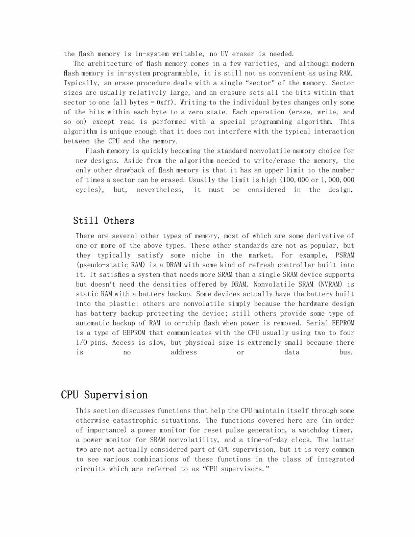
CPU Supervision
This section discusses functions that help the CPU maintain itself through some
otherwise catastrophic situations. The functions covered here are (in order
of importance) a power monitor for reset pulse generation, a watchdog timer,
a power monitor for SRAM nonvolatility, and a time-of-day clock. The latter
two are not actually considered part of CPU supervision, but it is very common
to see various combinations of these functions in the class of integrated
circuits which are referred to as “CPU supervisors.”
Reset
Before the CPU can do anything at all, it needs to be powered up, which simply
requires a connection to the power and ground pins on the device. Once powered
up, it’s essential that the internals of the device are allowed to synchronize and start up in a sane state. A RESET signal forces key CPU components to a
known initial state.
Typical requirements on a reset input line of a processor are that it be held
in a constant active (usually low) state for some duration (say 100ms). In some
designs, a simple resistor/capacitor (RC) combination is used to keep the RESET
line in a low state for the 100ms time period when power is applied to the system
(this is referred to as power-on reset).
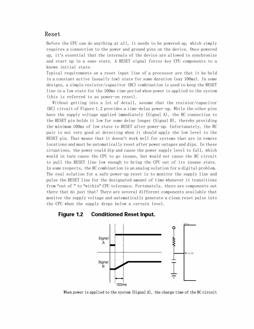
Without getting into a lot of detail, assume that the resistor/capacitor
(RC) circuit of Figure 1.2 provides a time-delay power-up. While the other pins
have the supply voltage applied immediately (Signal A), the RC connection to
the RESET pin holds it low for some delay longer (Signal B), thereby providing
the minimum 100ms of low state to RESET after power-up. Unfortunately, the RC
pair is not very good at detecting when it should apply the low level to the
RESET pin. That means that it doesn’t work well for systems that are in remote locations and must be automatically reset after power outages and dips. In these
situations, the power could dip and cause the power supply level to fall, which
would in turn cause the CPU to go insane, but would not cause the RC circuit
to pull the RESET line low enough to bring the CPU out of its insane state.
In some respects, the RC combination is an analog solution for a digital problem.
The real solution for a safe power-up reset is to monitor the supply line and
pulse the RESET line for the designated amount of time whenever it transitions
from “out of ” to “within” CPU tolerance. Fortunately, there are components out there that do just that! There are several different components available that
monitor the supply voltage and automatically generate a clean reset pulse into
the CPU when the supply drops below a certain level.
When power is applied to the system (Signal A), the charge time of the RC circuit
attached to the reset input (Signal B) delays the reset activation. While this
reset mechanism works when the power is cycled cleanly, it can cause problems
when power is momentarily interrupted.
Watchdog Timer
The watchdog timer (WDT) acts as a safety net for the system. If the software
stops responding or attending to the task at hand, the watchdog timer detects
that something is amiss and resets the software automatically. The system might
stop responding as a result of any number of difficult-to-detect hardware or firmware defects. For example, if an unusual condition causes a buffer overrun that corrupts the stack frame, some function’s return address could be overwritten. When that function completes, it then returns to the wrong spot
leaving the system utterly confused. Runaway pointers (firmware) or a glitch on the data bus (hardware) can cause similar crashes. Different external factors
can cause “glitches.” For example, even a small electrostatic discharge near the device might cause enough interference to momentarily change the state of
one bit on the address or data bus. Unfortunately, these kinds of defects can
be very intermittent, making them easy to miss during the project’s system test stage.
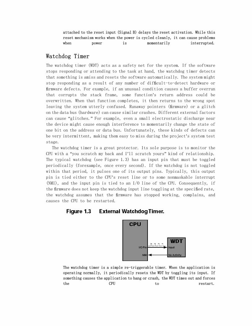
The watchdog timer is a great protector. Its sole purpose is to monitor the
CPU with a “you scratch my back and I’ll scratch yours” kind of relationship. The typical watchdog (see Figure 1.3) has an input pin that must be toggled
periodically (forexample, once every second). If the watchdog is not toggled
within that period, it pulses one of its output pins. Typically, this output
pin is tied either to the CPU’s reset line or to some nonmaskable interrupt (NMI), and the input pin is tied to an I/O line of the CPU. Consequently, if
the firmware does not keep the watchdog input line toggling at the specified rate, the watchdog assumes that the firmware has stopped working, complains, and causes the CPU to be restarted.
The watchdog timer is a simple re-triggerable timer. When the application is
operating normally, it periodically resets the WDT by toggling its input. If
something causes the application to hang or crash, the WDT times out and forces
the CPU to restart.
Battery-Backed SRAM
Not all systems need to maintain the integrity of their SRAM when power is turned
off, but this requirement is becoming more and more common because the compo-
nents that provide that capability are getting cheaper and easier to use. Not
too long ago, embedded systems used an arrangement of discrete components to
determine what voltage was higher (power supply or battery) and properly steer
the higher supply to the power pin of the SRAM (or the whole system). Now a
handful of companies provide nonvolatile SRAM modules that have the battery
and the power supply monitoring circuitry built right into the part. These parts
are guaranteed to retain data for up to 10 years (with certain restrictions
regarding the actual amount of time the internal battery is powering the SRAM,
of course). Modules with built-in batteries are often available in versions
that are pin-compatible with standard SRAM chips. These pin-compatible packages
can be a life-saver if you need to add nonvolatile read/write storage to an
existing design.
Time-of-Day Clock
For most embedded systems, the CPU provides all that is needed for maintaining
time. Typically, there is no need to keep track of the time of day; nevertheless,
when you need the time of day, you can’t get it without some type of battery-backed time-of-day clock function. Even though the CPU has its own
crystal and can keep relatively good time, the CPU’s notion of time only persists as long as the CPU is powered up and running. When the board is reset, the CPU’s clock is reset as well, making it impossible for the CPU to maintain the time
on its own. If you need time of day in your system, then you need a battery
and a time-of-day chip. An exception to this case is if the embedded system
knows that it has an external device from which it can get the current time
after being reset.
Serial Port Drivers
Many embedded systems use serial ports as an interface to the outside world.
Despite the serial port’s age (it has been around longer than dirt), serial ports are still found on most modern single-board computers. The serial device
on an embedded system has two portions: the protocol and the physical interface.
The protocol portion takes care of start and stop bits, bits per character,
the width of each bit based on a configured baud rate, and the conversion of the serial bit stream into a parallel byte stream easily digested by the CPU.
The physical interface takes care of converting voltage levels on the CPU to
the voltage levels needed by the interface. In many cases, the physical
interface also provides some electrical isolation between the physical
connector and the CPU. Embedded systems use two fundamentally different
transmission mechanisms for their serial ports: single wire and differential
drive transmission.
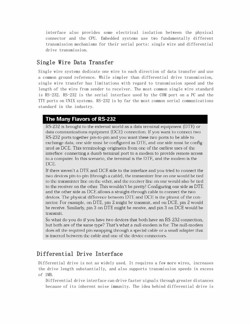
Single Wire Data Transfer
Single wire systems dedicate one wire to each direction of data transfer and use
a common ground reference. While simpler than differential drive transmission,
single wire transfer has limitations with regard to transmission speed and the
length of the wire from sender to receiver. The most common single wire standard
is RS-232. RS-232 is the serial interface used by the COM port on a PC and the
TTY ports on UNIX systems. RS-232 is by far the most common serial communications
standard in the industry.
Differential Drive Interface
Differential drive is not as widely used. It requires a few more wires, increases
the drive length substantially, and also supports transmission speeds in excess
of 1MB.
Differential drive interface can drive faster signals through greater distances
because of its inherent noise immunity. The idea behind differential drive is
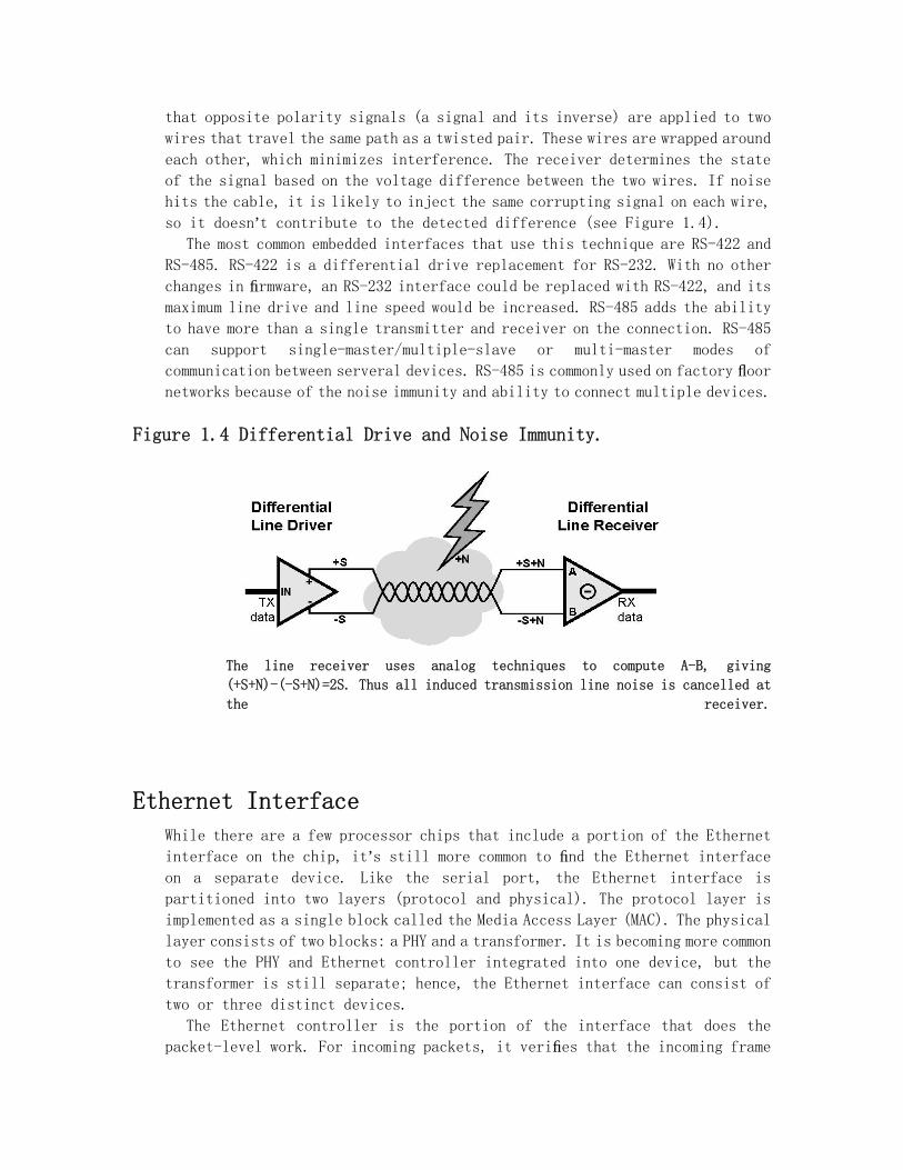
that opposite polarity signals (a signal and its inverse) are applied to two
wires that travel the same path as a twisted pair. These wires are wrapped around
each other, which minimizes interference. The receiver determines the state
of the signal based on the voltage difference between the two wires. If noise
hits the cable, it is likely to inject the same corrupting signal on each wire,
so it doesn’t contribute to the detected difference (see Figure 1.4). The most common embedded interfaces that use this technique are RS-422 and
RS-485. RS-422 is a differential drive replacement for RS-232. With no other
changes in firmware, an RS-232 interface could be replaced with RS-422, and its maximum line drive and line speed would be increased. RS-485 adds the ability
to have more than a single transmitter and receiver on the connection. RS-485
can support single-master/multiple-slave or multi-master modes of
communication between serveral devices. RS-485 is commonly used on factory floor networks because of the noise immunity and ability to connect multiple devices.
Figure 1.4 Differential Drive and Noise Immunity.
The line receiver uses analog techniques to compute A-B, giving
(+S+N)-(-S+N)=2S. Thus all induced transmission line noise is cancelled at
the receiver.
Ethernet Interface
While there are a few processor chips that include a portion of the Ethernet
interface on the chip, it’s still more common to find the Ethernet interface on a separate device. Like the serial port, the Ethernet interface is
partitioned into two layers (protocol and physical). The protocol layer is
implemented as a single block called the Media Access Layer (MAC). The physical
layer consists of two blocks: a PHY and a transformer. It is becoming more common
to see the PHY and Ethernet controller integrated into one device, but the
transformer is still separate; hence, the Ethernet interface can consist of
two or three distinct devices.
The Ethernet controller is the portion of the interface that does the
packet-level work. For incoming packets, it verifies that the incoming frame
has a valid cyclic redundancy check (CRC), ignores packets that do not match
a specified MAC address, organizes the incoming frames as packets that can be retrieved by the CPU (usually through either a FIFO or DMA transfer), and
generates interrupts based on various configuration parameters established by the driver. For outgoing packets, the Ethernet controller calculates the CRC,
transfers data from memory to the PHY, adds padding to small packets, and
interrupts the CPU to indicate that the packet has been sent.
The PHY takes care of the lowest level of the interface protocol. It is
responsible for various parameters (like bit rate) specific to the environment. The transformer provides isolation and electrical conversion of the signals
passed over the cable.
Flash Device Options
All flash devices are structured as a number of sectors. On some devices, the sectors are all the same size; on others the sector sizes vary. Some have
features that allow the firmware to lock a sector so that it cannot be erased unless a physical connection is inserted onto the hardware. Some devices have
reset input lines, and others do not. Densities vary from 64KB to 8MB in a single
flash device.
Flash Locking Facilities
Erasing or writing flash memory involves a special, nontrivial algorithm. Thus, it is relatively safe to assume that this algorithm will not be executed
accidentally. However, it is still nice to have the option to protect certain
sectors from misbehaving code. Many of the available flash devices have the ability to protect one or more sectors from write operations. Some of these
devices allow you to protect a specified sector or group of sectors by placing the device in an external programming device and applying a high voltage to
one of the pins. Others have a more flexible configuration that uses an external write protect pin and a lock sequence. In this latter type of device, a sector
is write-protected or locked by executing a specific command sequence. Once locked, a sector can only be modified after first being unlocked. This process makes it even more difficult to corrupt a sector accidentally. Locking can be used to assure that some very basic boot code is always available for the CPU
regardless of what happens to the programming of the other sectors.
If this safeguard is still not enough, an alternate technique can prevent
a sector from being modified until a power cycle occurs. This method is typically accomplished by enabling the write-protect pin and then initiating the lock
sequence to a particular device sector. Because there is no unlock sequence
that works when the write-protect pin is enabled and the write protect pin can
not change state until the next hard reset, the sector is protected from all
erroneous writes except those that happen immediately upon boot. If you need
more protection than this method provides, use EPROM!
Bottom-Boot and Top-Boot Flash Devices
Some devices are organized as a few small sectors at the bottom address space,
followed by large sectors that fill the remaining space. Some devices have a few small sectors at the top of the device’s address space and use large sectors in the lower address space. Since boot code is typically placed in small sectors,
flash memory is some times described as bottom-boot or top-boot, depending on where the smaller sectors are located.
Ultimately, one sector contains the memory space that the CPU accesses as
a result of a power cycle or reset (boot). This sector is usually referred to
as the boot sector. Because some CPUs have a reset vector that is at the top of memory space and others have a reset vector at the bottom of memory space,
the flash devices come in bottom-boot and top-boot flavors. A processor that boots to the top of memory space would probably use a top-boot device, and a processor
that boots to the bottom of its memory space would be more suited to a bottom-boot
device.
When the boot sector of the flash device exists in the boot-time address space of the CPU, it can be protected by making the boot sectors unmodifiable. Since only a small amount of code is typically needed to provide a basic boot, there
is little wasted space if you dedicate a small sector to an unmodifiable boot routine. This supports the ability to make as much of the flash space in-system reprogrammable without losing the security of knowing that if all of the
reprogrammable flash was accidentally corrupted, the system would still be able to boot through the small amount of code in the unmodifiable boot sector.
The CPU/Memory Interface
The most critical interface in any computing system is the connection between
memory and the CPU. If this interface doesn’t function properly, the CPU cannot function because it cannot retrieve instructions. If the processor can’t reliably retrieve instructions, it really doesn’t matter if anything else on the board works — you won’t be using it anyway.
Understanding the CPU/memory interface is important to more than just the
data and instruction stream. In most systems, peripherals share the data and
address buses with memory. Thus, understanding the protocol for these buses
is important to understanding much of the hardware.
This section explains, in general terms, how the CPU uses the address and
data buses to communicate with other parts of the system. To make the discussion
more concrete, I describe the operation in terms of the hypothetical machine
detailed in the simplified schematics in Figure 1.5 and Figure 1.6. Don’t worry,
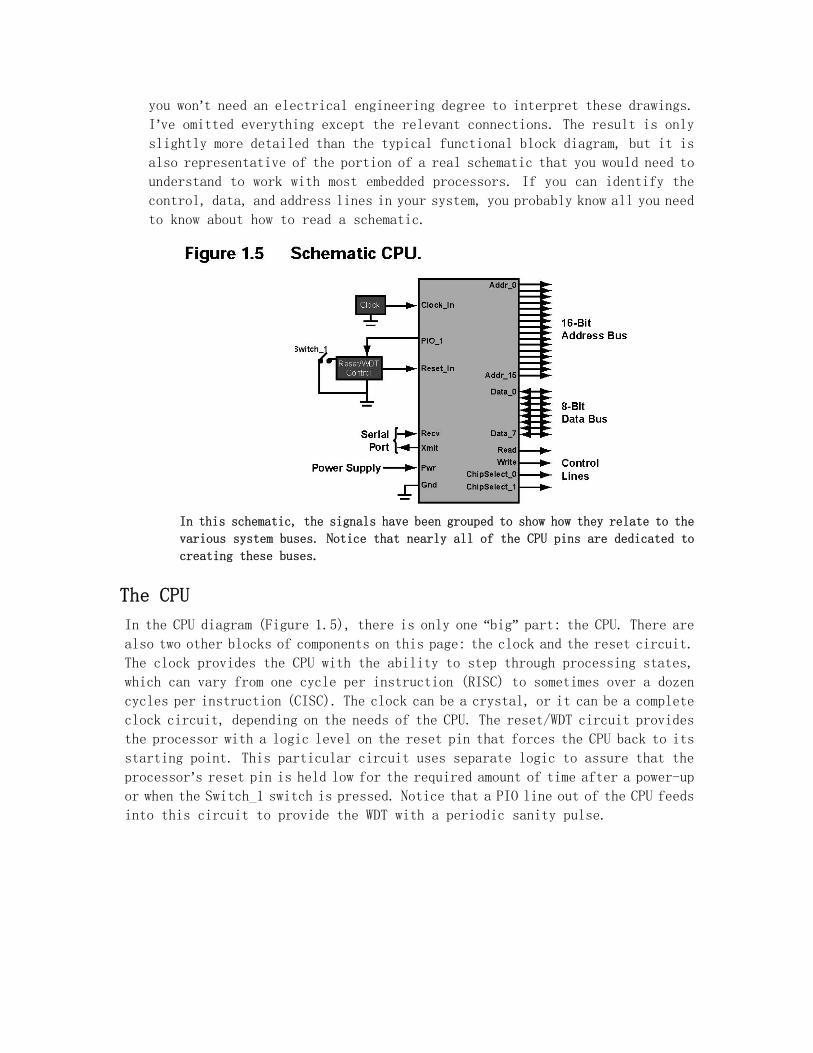
you won’t need an electrical engineering degree to interpret these drawings. I’ve omitted everything except the relevant connections. The result is only slightly more detailed than the typical functional block diagram, but it is
also representative of the portion of a real schematic that you would need to
understand to work with most embedded processors. If you can identify the
control, data, and address lines in your system, you probably know all you need
to know about how to read a schematic.
In this schematic, the signals have been grouped to show how they relate to the
various system buses. Notice that nearly all of the CPU pins are dedicated to
creating these buses.
The CPU
In the CPU diagram (Figure 1.5), there is only one “big” part: the CPU. There are also two other blocks of components on this page: the clock and the reset circuit.
The clock provides the CPU with the ability to step through processing states,
which can vary from one cycle per instruction (RISC) to sometimes over a dozen
cycles per instruction (CISC). The clock can be a crystal, or it can be a complete
clock circuit, depending on the needs of the CPU. The reset/WDT circuit provides
the processor with a logic level on the reset pin that forces the CPU back to its
starting point. This particular circuit uses separate logic to assure that the
processor’s reset pin is held low for the required amount of time after a power-up or when the Switch_1 switch is pressed. Notice that a PIO line out of the CPU feeds
into this circuit to provide the WDT with a periodic sanity pulse.
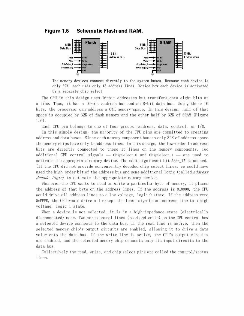
The memory devices connect directly to the system buses. Because each device is
only 32K, each uses only 15 address lines. Notice how each device is activated
by a separate chip select.
The CPU in this design uses 16-bit addresses but transfers data eight bits at
a time. Thus, it has a 16-bit address bus and an 8-bit data bus. Using these 16
bits, the processor can address a 64K memory space. In this design, half of that
space is occupied by 32K of flash memory and the other half by 32K of SRAM (Figure 1.6).
Each CPU pin belongs to one of four groups: address, data, control, or I/O.
In this simple design, the majority of the CPU pins are committed to creating
address and data buses. Since each memory component houses only 32K of address space
the memory chips have only 15 address lines. In this design, the low-order 15 address
bits are directly connected to these 15 lines on the memory components. Two
additional CPU control signals — ChipSelect_0 and ChipSelect_1 — are used to
activate the appropriate memory device. The most significant bit Addr_15 is unused. (If the CPU did not provide conveniently decoded chip select lines, we could have
used the high-order bit of the address bus and some additional logic (called address decode logic) to activate the appropriate memory device.
Whenever the CPU wants to read or write a particular byte of memory, it places
the address of that byte on the address lines. If the address is 0x0000, the CPU
would drive all address lines to a low voltage, logic 0 state. If the address were
0xFFFE, the CPU would drive all except the least significant address line to a high voltage, logic 1 state.
When a device is not selected, it is in a high-impedance state (electrically
disconnected) mode. Two more control lines (read and write) on the CPU control how
a selected device connects to the data bus. If the read line is active, then the
selected memory chip’s output circuits are enabled, allowing it to drive a data value onto the data bus. If the write line is active, the CPU’s output circuits are enabled, and the selected memory chip connects only its input circuits to the
data bus.
Collectively the read, write, and chip select pins are called the control/status
lines.
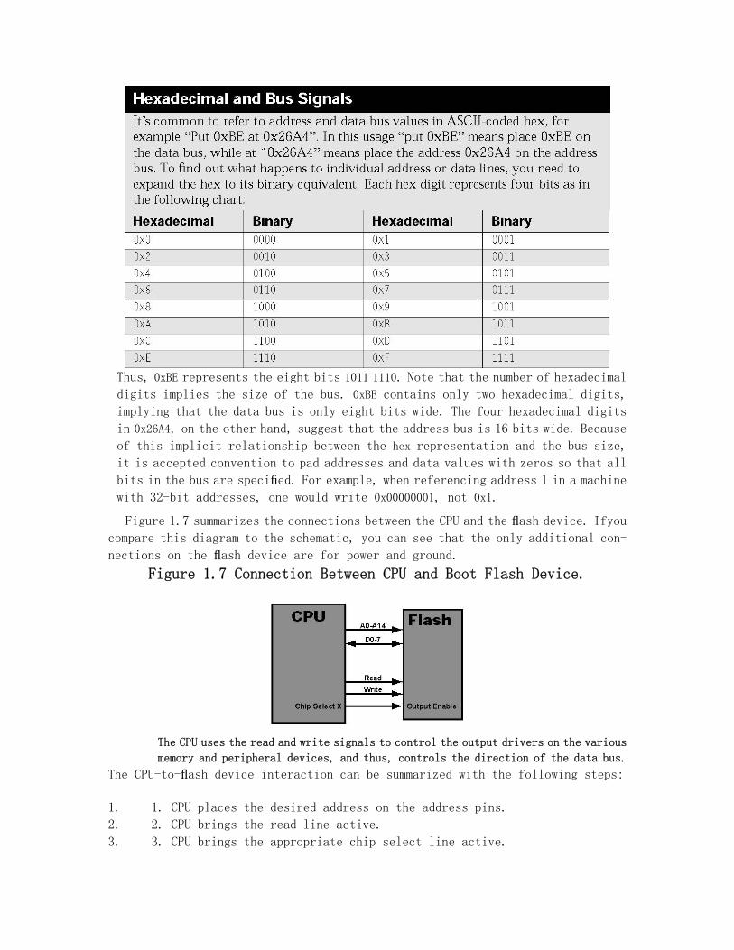
Thus, 0xBE represents the eight bits 1011 1110. Note that the number of hexadecimal
digits implies the size of the bus. 0xBE contains only two hexadecimal digits,
implying that the data bus is only eight bits wide. The four hexadecimal digits
in 0x26A4, on the other hand, suggest that the address bus is 16 bits wide. Because
of this implicit relationship between the hex representation and the bus size,
it is accepted convention to pad addresses and data values with zeros so that all
bits in the bus are specified. For example, when referencing address 1 in a machine with 32-bit addresses, one would write 0x00000001, not 0x1.
Figure 1.7 summarizes the connections between the CPU and the flash device. Ifyou compare this diagram to the schematic, you can see that the only additional con-
nections on the flash device are for power and ground. Figure 1.7 Connection Between CPU and Boot Flash Device.
The CPU uses the read and write signals to control the output drivers on the various
memory and peripheral devices, and thus, controls the direction of the data bus.
The CPU-to-flash device interaction can be summarized with the following steps:
1. 1. CPU places the desired address on the address pins.
2. 2. CPU brings the read line active.
3. 3. CPU brings the appropriate chip select line active.
4. 4. The flash device places the data located at the specified address onto the data bus.
5. 5. CPU reads in the data that has been placed on the bus by the flash device. 6. 6. CPU releases the chip select line and processes the data. This sequence
of steps allows the CPU to retrieve the bytes from memory that ultimately become
instructions. It’s commonly referred to as instruction fetching. If you understand this interface, it’s easy to connect to other devices, because they are all fundamentally the same. The SRAM interface is identical except that a different
chip select line is activated. The different chip select lines are configured so that each line is active for a 32K address space. (ChipSelect_0 is used for the 0–32K range, and ChipSelect_1 is used for the 32K–64K range.) A write access is essentially the same thing except that now the Write line is used and the data flow is from CPU to memory, not memory to CPU. So that’s essentially it for the address, data, and control. You have a certain number of address bits (dependent on the actual size
of the device), 8 data bits (16 or 32 if you were using a different device), and
a few control lines (read, write, and chip select). All that remains in the schematic
is the serial port. Since most modern processors have a UART built in, there’s only a driver to attach, and that does not
involve any CPU interaction. In other words, you now understand the fundamentals
of a simple microprocessor-based hardware design!
The Power (and Pitfalls) of Cache
For standard programming environments, cache is a blessing. It provides a real
speed increase for code that is written to use it properly (refer to Figure
1.8). Caching takesadvantage of a phenomenon known as locality of reference.1
Locality of reference states that at any given point in a program’s execution, the CPU is accessing some small block of memory repeatedly. The ability to pull
that small block of memory into a faster memory area is a very effective way
to speed up what would otherwise be a relatively slow rate of memory access.
Figure 1.8 Cache Between CPU and External Devices.
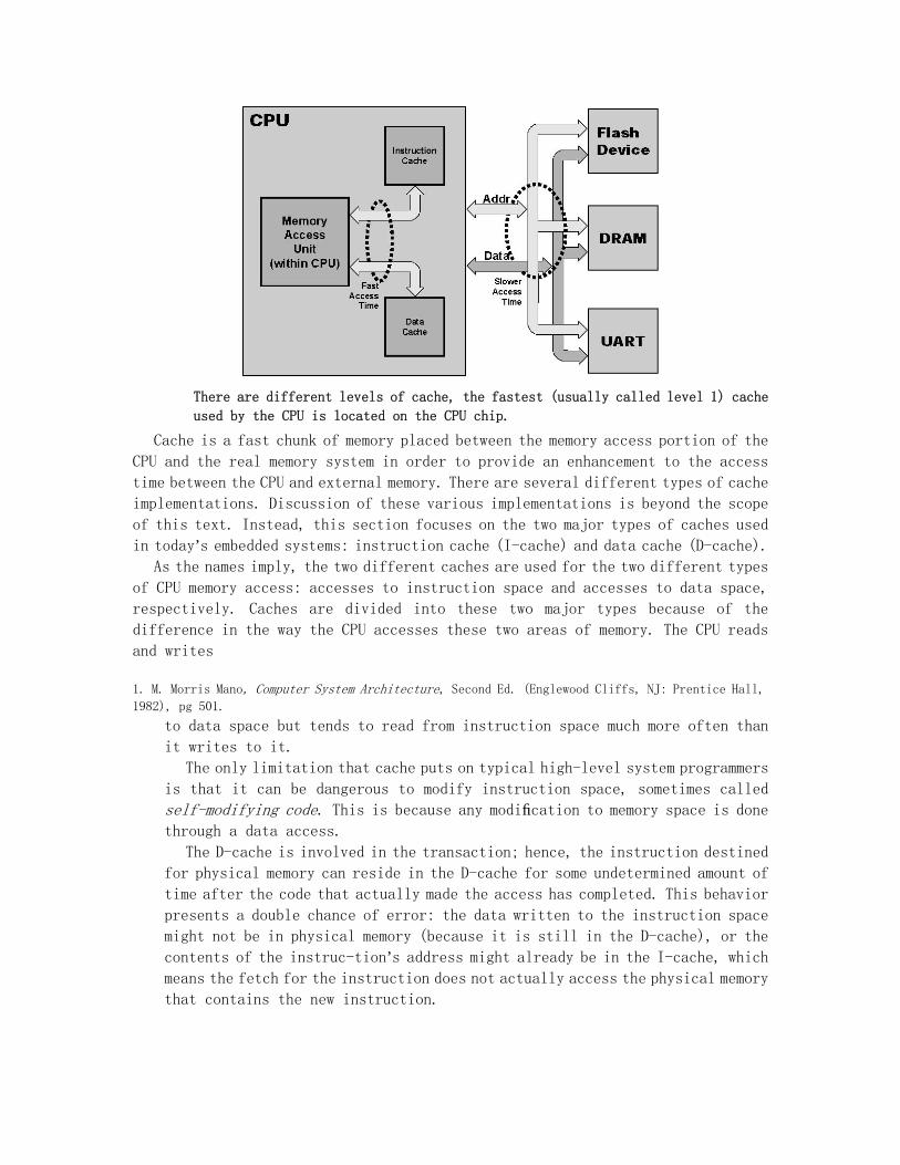
There are different levels of cache, the fastest (usually called level 1) cache
used by the CPU is located on the CPU chip.
Cache is a fast chunk of memory placed between the memory access portion of the
CPU and the real memory system in order to provide an enhancement to the access
time between the CPU and external memory. There are several different types of cache
implementations. Discussion of these various implementations is beyond the scope
of this text. Instead, this section focuses on the two major types of caches used
in today’s embedded systems: instruction cache (I-cache) and data cache (D-cache). As the names imply, the two different caches are used for the two different types
of CPU memory access: accesses to instruction space and accesses to data space,
respectively. Caches are divided into these two major types because of the
difference in the way the CPU accesses these two areas of memory. The CPU reads
and writes
1. M. Morris Mano, Computer System Architecture, Second Ed. (Englewood Cliffs, NJ: Prentice Hall, 1982), pg 501.
to data space but tends to read from instruction space much more often than
it writes to it.
The only limitation that cache puts on typical high-level system programmers
is that it can be dangerous to modify instruction space, sometimes called
self-modifying code. This is because any modification to memory space is done through a data access.
The D-cache is involved in the transaction; hence, the instruction destined
for physical memory can reside in the D-cache for some undetermined amount of
time after the code that actually made the access has completed. This behavior
presents a double chance of error: the data written to the instruction space
might not be in physical memory (because it is still in the D-cache), or the
contents of the instruc-tion’s address might already be in the I-cache, which means the fetch for the instruction does not actually access the physical memory
that contains the new instruction.
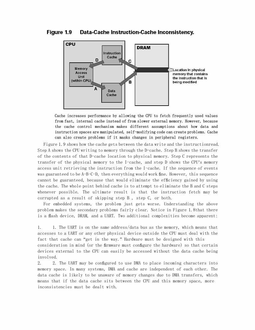
Cache increases performance by allowing the CPU to fetch frequently used values
from fast, internal cache instead of from slower external memory. However, because
the cache control mechanism makes different assumptions about how data and
instruction spaces are manipulated, self-modifying code can create problems. Cache
can also create problems if it masks changes in peripheral registers.
Figure 1.9 shows how the cache gets between the data write and the instructionread.
Step A shows the CPU writing to memory through the D-cache. Step B shows the transfer
of the contents of that D-cache location to physical memory. Step C represents the
transfer of the physical memory to the I-cache, and step D shows the CPU’s memory access unit retrieving the instruction from the I-cache. If the sequence of events
was guaranteed to be A-B-C-D, then everything would work fine. However, this sequence cannot be guaranteed, because that would eliminate the efficiency gained by using the cache. The whole point behind cache is to attempt to eliminate the B and C steps
whenever possible. The ultimate result is that the instruction fetch may be
corrupted as a result of skipping step B , step C, or both.
For embedded systems, the problem just gets worse. Understanding the above
problem makes the secondary problems fairly clear. Notice in Figure 1.8that there
is a flash device, DRAM, and a UART. Two additional complexities become apparent:
1. 1. The UART is on the same address/data bus as the memory, which means that
accesses to a UART or any other physical device outside the CPU must deal with the
fact that cache can “get in the way.” Hardware must be designed with this consideration in mind (or the firmware must configure the hardware) so that certain devices external to the CPU can easily be accessed without the data cache being
involved.
2. 2. The UART may be configured to use DMA to place incoming characters into memory space. In many systems, DMA and cache are independent of each other. The
data cache is likely to be unaware of memory changes due to DMA transfers, which
means that if the data cache sits between the CPU and this memory space, more
inconsistencies must be dealt with.
The complexity of the hardware and the “need for speed” make these issues tricky but not insurmountable. Most of the prior problems are solved through good hard-
ware and firmware design. The initial issue of I-cache and D-cache inconsistency can be resolved by invoking a flush of the data cache and an invalidation of the instruction cache. A flush forces the content of the data cache out to the real memory. An invalidation empties the instruction cache so that future CPU requests retrieve
a fresh copy of corresponding memory.
Also, there are some characteristics of cache that can help resolve these
problems. For example, a write through data cache ensures that data written to memory is placed in cache but also written out to physical memory. This guarantees that
data writes will be loaded to cache and will pass through the cache to real memory;
hence it really only provides a speed improvement for data reads. Also, a facility
in some CPUs called bus snooping helps with the memory inconsistency issues related to DMA and cache. Bus snooping hardware detects when DMA is used to access memory
space that is cached and automatically invalidates the corresponding cache loca-
tions. Bus snooping hardware isn’t available on all systems however. Additionally, to avoid the problem with cache being between the CPU and the UART, devices can
usually be mapped to a memory location that doesn’t involve the cache at all. It is very common for a CPU to restrict caching to certain specific cachable regions of memory, rather than designating its entire memory space cacheable. The bottom
line is that the firmware developer must be aware of these hardware and firmware capa-bilities and limitations in order to deal with these complexities efficiently.
Summary
While embedded systems come in a fascinating array of variations, at the lowest
hardware levels they usually have many general similarities. Memory systems
interface with CPU via address and data buses. Systems interface with
development hosts via serial ports. Watchdog timers supply robust operation
even in the presence of intermittent software and hardware bugs. Knowing the
general structure of these common facilities gives you a useful framework for
learning the specifics of new systems. The hardware coverage in this chapter won’t make you a hardware guru, but
it should prepare you to better understand the documentation for your particular
hardware. More importantly (for the purposes of the book), it should prepare
you to understand the hardware issues discussed in later chapters.
Where this chapter described primarily hardware features, the next chapter
focuses on software issues — specifically on how to compile and load programs for an embedded target. More than anything else, these two issues, the need
for greater knowledge about the hardware and the need for tools that work in
a cross-develop-ment environment, separate embedded systems from application
development.

Related Documents