May 2007 Page 5 The Simulation Standard Electrical Stress Degradation of Small-Grain Polysilicon Thin-Film Transistors Domenico Palumbo, Silvia Masala, Paolo Tassini, Alfredo Rubino, and Dario della Sala Copyright © 2007 IEEE. Reprinted from IEEE Transactions on Electron Devices, VOL 54, NO 3, March 2007. Abstract—This paper is focused on the stability of n- channel laser-crystallized polysilicon thin-film transis- tors (TFTs) submitted to a hydrogenation process during the fabrication and with small grains dimension.With the aid of numerical simulations, we investigate the ef- fects of static stress using two types of procedures: the on stress and the hot carrier stress. Results show that the variations of trap state density into the whole polysilicon layer and not only near the drain junction are responsi- ble for the degradation of TFTs performances in both the two types of stress and that the interface trap states play a negligible role compared to the bulk trap states. Index Terms—Density-of-states (DoS), fixed charge, nu- merical simulation, reliability, thin-film transistor (TFTs). I. Introduction LASER-CRYSTALLIZED polycrystalline silicon thin- film transistors (TFTs), processed at a low temperature (below 600 o C), are devices of great importance in the mi- croelectronics industry since they are currently widely used in active-matrix liquid crystal displays and are suit- able for the emerging activematrix organic light emitting displays (AMOLED) [1]. By using low laser energy densities up to 200 mJ/cm 2 , we have fabricated devices with small grains dimension with a mobility of up to about 3 cm 2 /V . s. These n-TFTs are suitable not only to drive an OLED diode [1], [2] but also to realize the row drivers [3]; moreover, the increased uniformity of electrical parameters, compared to large grains size TFTs, gives rise to a reduction, for instance, of the threshold voltage spreading [4], avoiding more com- plicated pixel circuit to overcome this problem [5], [6] and obtaining brightness uniformity over large areas. Their drawback is the instability after electrical stress [7], [8], due to a high density of in-grain and grain boundary defects, to poor properties of the gate insulator and to poor polysilicon/ oxide interface [9]. The purpose of this paper is to understand which are the main mechanisms originating from device degradation under a bias stress. This is accomplished by comparing the computer simulation of device characteristics with the experimental data. II. Fabrication Details Polysilicon TFTs were fabricated on 1737 Corning glass substrate by low temperature processes. An amorphous silicon film, 100-nm thick, was deposited by plasma enhanced chemical vapor deposition (PECVD) at 200 o C and 0.75 torr using pure SiH 4 (20 sccm). The source and drain regions were obtained by the PECVD deposition of an n-type layer, 23-nm thick ( T = 120 o C, p = 0.75 torr, with a SiH 4 /PH 3 98/2 gas ratio, and 20 sccm). For the patterning of the drain and source elec- trode areas, the lift-off method were used, with silicon oxide as the sacrificial layer. The a-Si:H, the sacrificial oxide, and the resist layers are deposited in sequence; after resist development and curing, the sacrificial layer is over etched by a buffered HF (a solution of HF and NH 4 F). This step determines, for the subsequently deposited n layer, a discontinuity which helps the resist lift off performed by acetone. In this way, the undesired n layer is removed as well. Next, the buffered HF bath completely removes the sacrificial oxide. The dehydrogenation before laser crystallization was per- formed, keeping the material for 8 h in vacuum at 450 o C. After the PECVD growth, the doped and undoped amor- phous films were crystallized by XeCl excimer laser irra- diation at λ = 308 nm, with a 130 x 13 mm beam diameter with a 200-mJ/cm 2 energy density on the sample. The active regions of TFTs were patterned by CF 4 plasma etching (CF 4 40 sccm, 0.35 torr, and rf power = 15 W). Then, a hydrogen plasma passivation was performed on Manuscript received May 10, 2006; revised October 2, 2006. This work was supported by Ministero dell’Istruzione dell’Università e della Ricerca in the framework of the FIRB Project Micropolys. The review of this paper was arranged by Editor G. Groeseneken. D. Palumbo, S. Masala, and P. Tassini are with the Italian National Agency for New Technologies, Energy and the Envi- ronment (ENEA) Research Center, 80055 Portici, Italy (e-mail: [email protected]). A. Rubino is with the DIIIE, University of Salerno, 84084 Fisci- ano (Salerno), Italy. D. della Sala is with the ENEA Research Center, 00060 S. Maria di Galeria (Rome), Italy. Digital Object Identifier 10.1109/TED.2006.890377

Welcome message from author
This document is posted to help you gain knowledge. Please leave a comment to let me know what you think about it! Share it to your friends and learn new things together.
Transcript
The Simulation Standard Page 4 May 2007 May 2007 Page 5 The Simulation Standard
Electrical Stress Degradation of Small-Grain Polysilicon Thin-Film Transistors
Domenico Palumbo, Silvia Masala, Paolo Tassini, Alfredo Rubino, and Dario della Sala
Copyright © 2007 IEEE.
Reprinted from IEEE Transactions on Electron Devices, VOL 54, NO 3, March 2007.
Abstract—This paper is focused on the stability of n-channel laser-crystallized polysilicon thin-fi lm transis-tors (TFTs) submitted to a hydrogenation process during the fabrication and with small grains dimension.With the aid of numerical simulations, we investigate the ef-fects of static stress using two types of procedures: the on stress and the hot carrier stress. Results show that the variations of trap state density into the whole polysilicon layer and not only near the drain junction are responsi-ble for the degradation of TFTs performances in both the two types of stress and that the interface trap states play a negligible role compared to the bulk trap states.
Index Terms—Density-of-states (DoS), fi xed charge, nu-merical simulation, reliability, thin-fi lm transistor (TFTs).
I. IntroductionLASER-CRYSTALLIZED polycrystalline silicon thin-fi lm transistors (TFTs), processed at a low temperature (below 600 oC), are devices of great importance in the mi-croelectronics industry since they are currently widely used in active-matrix liquid crystal displays and are suit-able for the emerging activematrix organic light emitting displays (AMOLED) [1].
By using low laser energy densities up to 200 mJ/cm2, we have fabricated devices with small grains dimension with a mobility of up to about 3 cm2/V . s. These n-TFTs are suitable not only to drive an OLED diode [1], [2] but also to realize the row drivers [3]; moreover, the increased uniformity of electrical parameters, compared to large grains size TFTs, gives rise to a reduction, for instance, of
the threshold voltage spreading [4], avoiding more com-plicated pixel circuit to overcome this problem [5], [6] and obtaining brightness uniformity over large areas.
Their drawback is the instability after electrical stress [7], [8], due to a high density of in-grain and grain boundary defects, to poor properties of the gate insulator and to poor polysilicon/ oxide interface [9].
The purpose of this paper is to understand which are the main mechanisms originating from device degradation under a bias stress. This is accomplished by comparing the computer simulation of device characteristics with the experimental data.
II. Fabrication DetailsPolysilicon TFTs were fabricated on 1737 Corning glass substrate by low temperature processes. An amorphous silicon fi lm, 100-nm thick, was deposited by plasma enhanced chemical vapor deposition (PECVD) at 200 oC and 0.75 torr using pure SiH4 (20 sccm).
The source and drain regions were obtained by the PECVD deposition of an n-type layer, 23-nm thick (T = T = T120 oC, p = 0.75 torr, with a SiH4/PH3 98/2 gas ratio, and 20 sccm). For the patterning of the drain and source elec-trode areas, the lift-off method were used, with silicon oxide as the sacrifi cial layer. The a-Si:H, the sacrifi cial oxide, and the resist layers are deposited in sequence; after resist development and curing, the sacrifi cial layer is over etched by a buffered HF (a solution of HF and NH4F). This step determines, for the subsequently deposited n layer, a discontinuity which helps the resist lift off performed by acetone. In this way, the undesired n layer is removed as well. Next, the buffered HF bath completely removes the sacrifi cial oxide.
The dehydrogenation before laser crystallization was per-formed, keeping the material for 8 h in vacuum at 450oC.
After the PECVD growth, the doped and undoped amor-phous fi lms were crystallized by XeCl excimer laser irra-diation at λ = 308 nm, with a 130 x 13 mm beam diameter with a 200-mJ/cm2 energy density on the sample.
The active regions of TFTs were patterned by CF4 plasma etching (CF4 40 sccm, 0.35 torr, and rf power = 15 W). Then, a hydrogen plasma passivation was performed on
Manuscript received May 10, 2006; revised October 2, 2006. This work was supported by Ministero dell’Istruzione dell’Università e della Ricerca in the framework of the FIRB Project Micropolys. The review of this paper was arranged by Editor G. Groeseneken.D. Palumbo, S. Masala, and P. Tassini are with the Italian National Agency for New Technologies, Energy and the Envi-ronment (ENEA) Research Center, 80055 Portici, Italy (e-mail: [email protected]).A. Rubino is with the DIIIE, University of Salerno, 84084 Fisci-ano (Salerno), Italy.D. della Sala is with the ENEA Research Center, 00060 S. Maria di Galeria (Rome), Italy.Digital Object Identifi er 10.1109/TED.2006.890377
The Simulation Standard Page 6 May 2007 May 2007 Page 7 The Simulation Standard
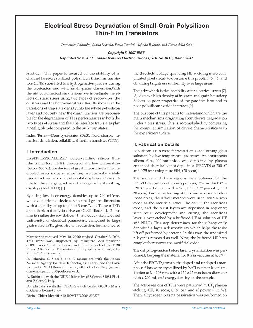
the polysilicon layer for 30 min at 400oC (p = 0.99 torr and rf power = 6 W) to reduce the defect density inside the fi lm and to improve the electrical characteristics of TFTs. The gate oxide, 100-nm thick, was deposited at 300oC and 0.40 torr by PECVD. Finally, the drain and source contact opening by wet etching (buffered HF), metal evapora-tion, and contact defi nition were performed to complete the structure (see Fig. 1). TFTs are produced through a four-mask process using the AZ5214E photo resist.
The geometrical parameters of the devices employed in this paper are: channel length (L) 5 µm and channel width (W) 40 µm.
Scanning electron microscopy analysis has shown that the polysilicon layer has a grain structure with an aver-age size of about 10 nm.
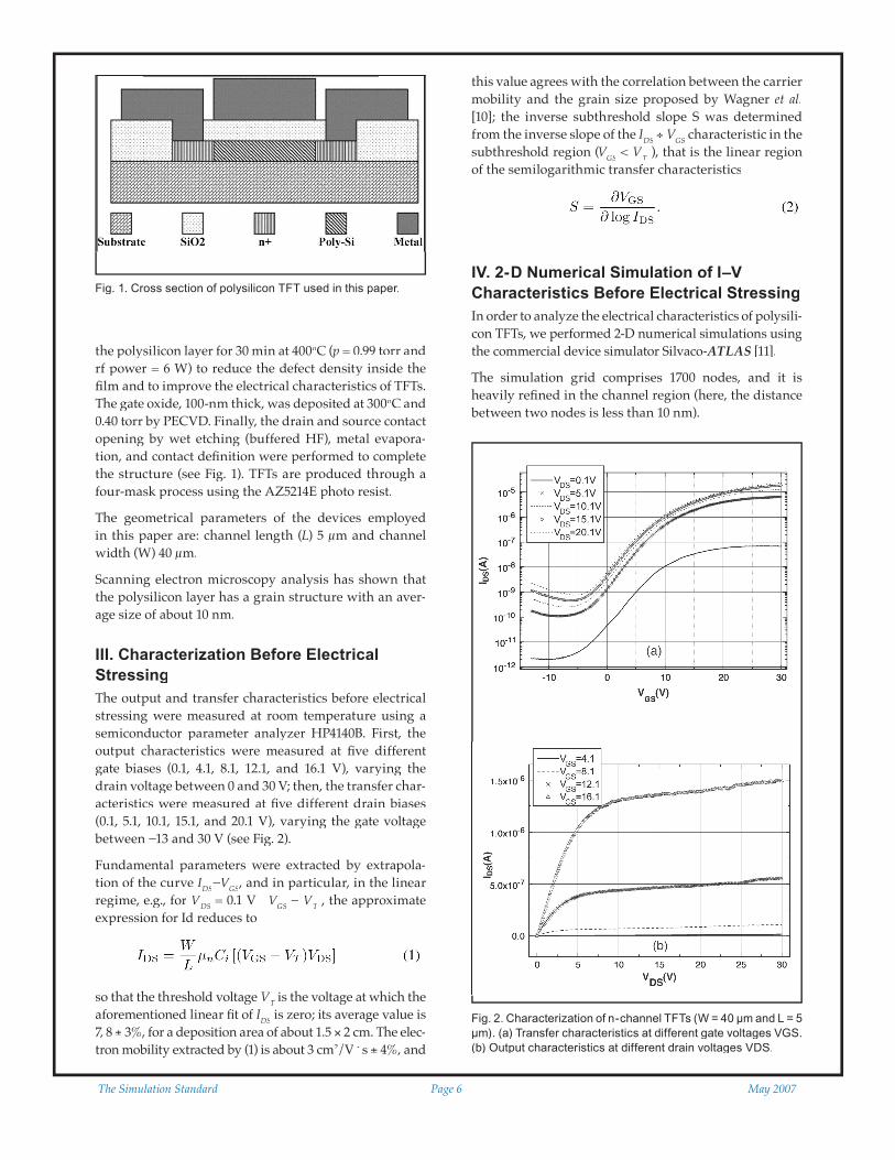
III. Characterization Before Electrical StressingThe output and transfer characteristics before electrical stressing were measured at room temperature using a semiconductor parameter analyzer HP4140B. First, the output characteristics were measured at fi ve different gate biases (0.1, 4.1, 8.1, 12.1, and 16.1 V), varying the drain voltage between 0 and 30 V; then, the transfer char-acteristics were measured at fi ve different drain biases (0.1, 5.1, 10.1, 15.1, and 20.1 V), varying the gate voltage between −13 and 30 V (see Fig. 2).
Fundamental parameters were extracted by extrapola-tion of the curve IDS−VGS−VGS−V , and in particular, in the linear regime, e.g., for VDS = 0.1 V VGSVGSV − VT , the approximate T , the approximate Texpression for Id reduces to
so that the threshold voltage VT is the voltage at which the T is the voltage at which the Taforementioned linear fi t of IDS is zero; its average value is 7, 8 ± 3%, for a deposition area of about 1.5 × 2 cm. The elec-tron mobility extracted by (1) is about 3 cm2/V . s ± 4%, and
this value agrees with the correlation between the carrier mobility and the grain size proposed by Wagner et al.[10]; the inverse subthreshold slope S was determined from the inverse slope of the IDS ÷ VGS VGS V characteristic in the subthreshold region (Vsubthreshold region (Vsubthreshold region ( GSVGSV < VT ), that is the linear region T ), that is the linear region Tof the semilogarithmic transfer characteristics
IV. 2-D Numerical Simulation of I–V Characteristics Before Electrical StressingIn order to analyze the electrical characteristics of polysili-con TFTs, we performed 2-D numerical simulations using the commercial device simulator Silvaco-ATLAS the commercial device simulator Silvaco-ATLAS the commercial device simulator Silvaco- [11].
The simulation grid comprises 1700 nodes, and it is heavily refi ned in the channel region (here, the distance between two nodes is less than 10 nm).
Fig. 1. Cross section of polysilicon TFT used in this paper.
Fig. 2. Characterization of n-channel TFTs (W = 40 µm and L = 5 µm). (a) Transfer characteristics at different gate voltages VGS. (b) Output characteristics at different drain voltages VDS.

The Simulation Standard Page 6 May 2007 May 2007 Page 7 The Simulation Standard
The fi ne grain structure of our polysilicon produces a large in-grain defect density; this is why our analysis is based on a continuous trap model, and we have simulat-ed a spatially uniform density-of-states, (DoS), through-out the volume of the polysilicon layer. Our fi lm can be considered as composed of small crystalline grains embedded in an amorphous tissue: the grain boundar-ies have a dimension comparable with the grain, so its properties, (Eg) and DoS, infl uence electron transport mechanisms, limiting, for instance, the mobility value and determining the overall electrical characteristics [12]. We have modeled the grain boundaries as a-Si:H.
It is worthwhile to point out that numerical simulation using a gap value of 1.12 eV does not fi t the experimental results. Instead, the best results are obtained with Eg =1.6 eV [13], [14].
The total DoS g(E) was modeled by the sum of two ex-ponential tails near the conduction and the valence and two deep level bands with Gaussian distribution (one ac-ceptorlike and the other donorlike). The model was [11]
The initial parameters of the upper-half gap DoS were obtained from experimental I–V curves using the meth-I–V curves using the meth-I–Vod by Suzuki et al. [15], [16], so that the interface states density has been considered negligible compared with the bulk states density. This assumption has been con-fi rmed by simulation.
The electron and hole mobilities were modeled as con-stant throughout the channel and independent of: 1) the transversal electric fi eld; 2) the gradient of the quasi-Fermi potentials; and 3) the doping level. The doping distribution was kept uniform throughout the polysili-con layer.
Table I summarizes the material parameters that pro-vides the best accordance with the experimental curves of realized devices, while the consequent DoS param-eters are: NTA = 9.2 . 1020 cm−3 . eV−1 eV−1 eV , NTD= 2.0 . 1021 cm−3
. eV−1 eV−1 eV , WTA= 0.1 eV, WTD = 0.1 eV, NGA = 5.0 . 1017 cm−3 .
eV−1eV−1eV , NGD = 1.0 . 1018 cm−3 . eV−1 eV−1 eV , EGA= 0.6 eV, EGD = 1.0 eV, WGA = 0.4 eV, and WGD = 0.4 eV.
An important issue is that, to simulate the transfer char-acteristics, we have to increase the density of the positive fi xed charge (QfQfQ ) at the interface between polysilicon f ) at the interface between polysilicon fand SiO2, from QfQfQ = 0.95 f = 0.95 f
. 1012 cm−2 for VDS = 0.1 V to 1.40 .
1012 cm−2 for VDS = 20.1 V, as shown in Fig. 3. The increase of the positive fi xed charge combined with a constant density of deep states reproduces the progressive shift of the subthreshold region observed during the charac-terizations, as a result from the good agreement between
Fig. 3. Fixed charge versus stressing time. The inset shows also VDS at which we measure the transfer characteristics.
Fig. 4. Simulated and experimental transfer characteristics of n-channel polysilicon TFT (W = 40µm) for V
DSV
DSV = 0.1, 5.1, 10.1,
DS = 0.1, 5.1, 10.1,
DS
15.1, and 20.1 V.
Table 1. Parameters used in the numerical simulation.
Parameters Description Values Units
mun Electrons mobility 3 cm2/Vs
mup Holes mobility 1 cm2/Vs
nv300 Valence band density of 2.5.1021 cm-3
states at 300K
nc300 Conduction band density 2.5.1021 cm-3
of states at 300K
eg300 Energy gap at 300k 1.6 eV
taun0 Shockley-Read-Hall 1.10-9 slifetime for electrons
taup0 Shockley-Read-Hall 1.10-9 slifetime for hole
The Simulation Standard Page 8 May 2007 May 2007 Page 9 The Simulation Standard
the experimental and simulated data shown in Fig. 4. Actually, during the characterization, we dynamically stress the devices, so we may suppose that these positive and negative bias stresses cause charge trapping in the gate oxide and alter the “fi xed-charge” at the interface between the oxide and semiconductor, producing a translation without any slope variation of the measured characteristics. Specifi cally, negative bias stress leads to positive charge trapping, which means an increase in the positive fi xed charge density; similarly, positive bias stress reduces the positive fi xed charge density, as ex-plained by Powell et al. [17]. The resulting total density of the fi xed charge depends on the global dynamic stress, and in our case, the positive fi xed charge increases with linear dependence on the stressing time. Instead, by changing the DoS in the bulk of the fi lm (varying the values of DoS parameters listed in this section) or the in-terface defect traps at discrete levels within the bandgap of the semiconductor (with the Atlas INTTRAP param-eter), the simulation failed to reproduce the shift of the subthreshold region observed in the experiments.
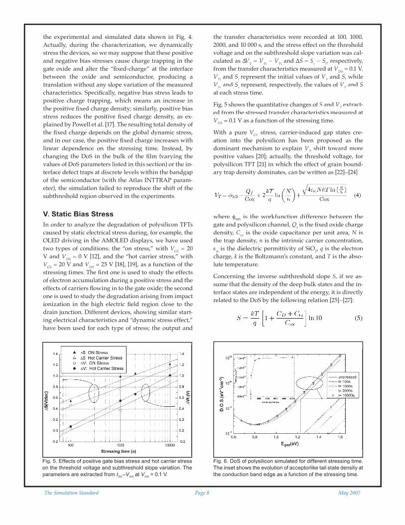
V. Static Bias StressIn order to analyze the degradation of polysilicon TFTs caused by static electrical stress during, for example, the OLED driving in the AMOLED displays, we have used two types of conditions: the “on stress,” with VGSVGSV = 20 V and VDS = 0 V [12], and the “hot carrier stress,” with VGSVGSV = 20 V and VDS = 25 V [18], [19], as a function of the stressing times. The fi rst one is used to study the effects of electron accumulation during a positive stress and the effects of carriers fl owing in to the gate oxide; the second one is used to study the degradation arising from impact ionization in the high electric fi eld region close to the drain junction. Different devices, showing similar start-ing electrical characteristics and “dynamic stress effect,” have been used for each type of stress; the output and
the transfer characteristics were recorded at 100, 1000, 2000, and 10 000 s, and the stress effect on the threshold voltage and on the subthreshold slope variation was cal-culated as ∆Vculated as ∆Vculated as ∆ T = T = T VTs − VTi and ∆S = Ss − Si, respectively, from the transfer characteristics measured at VDS = 0.1 V. VTi and Si represent the initial values of VT and T and T S, while VTs and Ss represent, respectively, the values of VT and T and T Sat each stress time.
Fig. 5 shows the quantitative changes of S and VT extract-T extract-Ted from the stressed transfer characteristics measured at VDS = 0.1 V as a function of the stressing time.
With a pure VGSVGSV stress, carrier-induced gap states cre-ation into the polysilicon has been proposed as the dominant mechanism to explain VT shift toward more T shift toward more Tpositive values [20]; actually, the threshold voltage, for polysilicon TFT [21] in which the effect of grain bound-ary trap density dominates, can be written as [22]–[24]
where φMS is the workfunction difference between the gate and polysilicon channel, QfQfQ is the fi xed oxide charge f is the fi xed oxide charge fdensity, Cox is the oxide capacitance per unit area, N is N is Nthe trap density, n is the intrinsic carrier concentration, εsi is the dielectric permittivity of SiO2, q is the electron charge, k is the Boltzmann’s constant, and k is the Boltzmann’s constant, and k T is the abso-T is the abso-Tlute temperature.
Concerning the inverse subthreshold slope S, if we as-sume that the density of the deep bulk states and the in-terface states are independent of the energy, it is directly related to the DoS by the following relation [25]–[27]:
Fig. 5. Effects of positive gate bias stress and hot carrier stress on the threshold voltage and subthreshold slope variation. The parameters are extracted from I
DS–V
GS–V
GS–V at
GS at
GSV
DSV
DSV = 0.1 V.
DS = 0.1 V.
DS
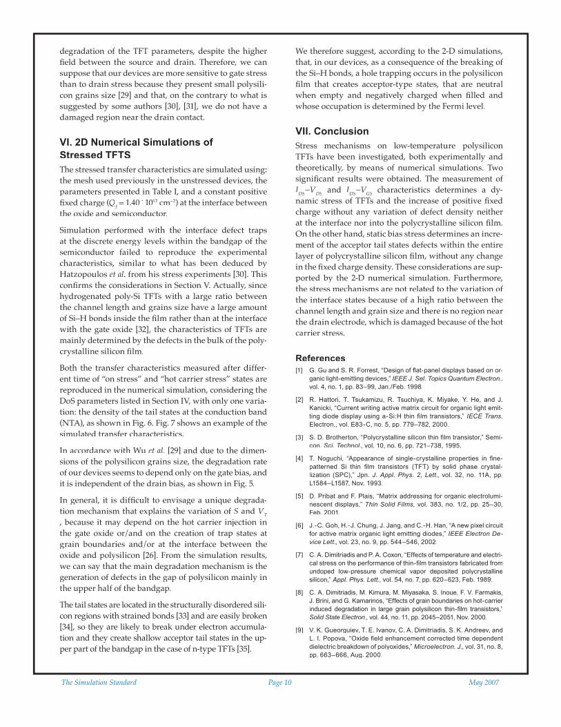
Fig. 6. DoS of polysilicon simulated for different stressing time. The inset shows the evolution of acceptorlike tail state density at the conduction band edge as a function of the stressing time.

The Simulation Standard Page 8 May 2007 May 2007 Page 9 The Simulation Standard
where CD is the depletion layer capacitance per unit area and Cts = q2Dts, with Dts (per square centimeter elec-tronvolt) as the density of the total trap states. For fully depleted TFTs with thin and intrinsic channel (in other words if the band bending occurs in the whole polysili-con layer), we have
where Dbulk (per cubic centimeter electronvolt) is the mean bulk trap density, Dit (per square centimeter elec-tronvolt) is the interface trap density, and tsi is the poly-silicon fi lm thickness.
Following the method of Rolland et al. [27] we have de-termined the upper values of Dbulk and bulk and bulk Dit for our TFTs
Although this method is not very precise, it permits a coarse estimation of relative trap density. In our TFTs, about 95% of Dts is due to the bulk states, and only 5% of Dts is due to the interface states.
Under “on stress” conditions, both S and VT show a T show a Tlogarithmic dependence on the stressing time (see Fig. 5): this behavior is consistent with a mechanism of stress-induced creation of acceptorlike traps, negatively charged when occupied by electrons [12], and means that the observed degradation effects are not caused by electron effects or charge injection into the gate di-electric, but they arise from the variation of bulk states density [28].
The degradation effects on the transfer characteristics af-ter 100, 1000, and 10 000 s of hot carrier stress are similar to those presented after positive gate bias stress condi-tions (see Fig. 5), also with the source and drain reversed. The application of an additional drain stressing bias to the gate stressing does not have a relevant effect on the
Fig. 7. Experimental and simulated transfer characteristics at different stressing times and at VDS = 0.1 V. (a) and (b) “On stress.” (c) and (d) “Hot carrier stress.”
The Simulation Standard Page 10 May 2007 May 2007 Page 11 The Simulation Standard
degradation of the TFT parameters, despite the higher fi eld between the source and drain. Therefore, we can suppose that our devices are more sensitive to gate stress than to drain stress because they present small polysili-con grains size [29] and that, on the contrary to what is suggested by some authors [30], [31], we do not have a damaged region near the drain contact.
VI. 2D Numerical Simulations of Stressed TFTSThe stressed transfer characteristics are simulated using: the mesh used previously in the unstressed devices, the parameters presented in Table I, and a constant positive fi xed charge (QfQfQ = 1.40 f = 1.40 f
. 1012 cm−2) at the interface between the oxide and semiconductor.
Simulation performed with the interface defect traps at the discrete energy levels within the bandgap of the semiconductor failed to reproduce the experimental characteristics, similar to what has been deduced by Hatzopoulos et al. from his stress experiments [30]. This confi rms the considerations in Section V. Actually, since hydrogenated poly-Si TFTs with a large ratio between the channel length and grains size have a large amount of Si–H bonds inside the fi lm rather than at the interface with the gate oxide [32], the characteristics of TFTs are mainly determined by the defects in the bulk of the poly-crystalline silicon fi lm.
Both the transfer characteristics measured after differ-ent time of “on stress” and “hot carrier stress” states are reproduced in the numerical simulation, considering the DoS parameters listed in Section IV, with only one varia-tion: the density of the tail states at the conduction band (NTA), as shown in Fig. 6. Fig. 7 shows an example of the simulated transfer characteristics.
In accordance with Wu et al. [29] and due to the dimen-sions of the polysilicon grains size, the degradation rate of our devices seems to depend only on the gate bias, and it is independent of the drain bias, as shown in Fig. 5.
In general, it is diffi cult to envisage a unique degrada-tion mechanism that explains the variation of S and VT, because it may depend on the hot carrier injection in the gate oxide or/and on the creation of trap states at grain boundaries and/or at the interface between the oxide and polysilicon [26]. From the simulation results, we can say that the main degradation mechanism is the generation of defects in the gap of polysilicon mainly in the upper half of the bandgap.
The tail states are located in the structurally disordered sili-con regions with strained bonds [33] and are easily broken [34], so they are likely to break under electron accumula-tion and they create shallow acceptor tail states in the up-per part of the bandgap in the case of n-type TFTs [35].
We therefore suggest, according to the 2-D simulations, that, in our devices, as a consequence of the breaking of the Si–H bonds, a hole trapping occurs in the polysilicon fi lm that creates acceptor-type states, that are neutral when empty and negatively charged when fi lled and whose occupation is determined by the Fermi level.
VII. ConclusionStress mechanisms on low-temperature polysilicon TFTs have been investigated, both experimentally and theoretically, by means of numerical simulations. Two signifi cant results were obtained. The measurement of IDS−VDS and IDS−VGS−VGS−V characteristics determines a dy-namic stress of TFTs and the increase of positive fi xed charge without any variation of defect density neither at the interface nor into the polycrystalline silicon fi lm. On the other hand, static bias stress determines an incre-ment of the acceptor tail states defects within the entire layer of polycrystalline silicon fi lm, without any change in the fi xed charge density. These considerations are sup-ported by the 2-D numerical simulation. Furthermore, the stress mechanisms are not related to the variation of the interface states because of a high ratio between the channel length and grain size and there is no region near the drain electrode, which is damaged because of the hot carrier stress.
References[1] G. Gu and S. R. Forrest, “Design of fl at-panel displays based on or-
ganic light-emitting devices,” IEEE J. Sel. Topics Quantum Electron., vol. 4, no. 1, pp. 83–99, Jan./Feb. 1998.
[2] R. Hattori, T. Tsukamizu, R. Tsuchiya, K. Miyake, Y. He, and J. Kanicki, “Current writing active matrix circuit for organic light emit-ting diode display using a-Si:H thin fi lm transistors,” IECE Trans. Electron., vol. E83-C, no. 5, pp. 779–782, 2000.
[3] S. D. Brotherton, “Polycrystalline silicon thin fi lm transistor,” Semi-con. Sci. Technol., vol. 10, no. 6, pp. 721–738, 1995.
[4] T. Noguchi, “Appearance of single-crystalline properties in fi ne-patterned Si thin fi lm transistors (TFT) by solid phase crystal-lization (SPC),” Jpn. J. Appl. Phys. 2, Lett., vol. 32, no. 11A, pp. L1584–L1587, Nov. 1993.
[5] D. Pribat and F. Plais, “Matrix addressing for organic electrolumi-nescent displays,” Thin Solid Films, vol. 383, no. 1/2, pp. 25–30, Feb. 2001.
[6] J.-C. Goh, H.-J. Chung, J. Jang, and C.-H. Han, “A new pixel circuit for active matrix organic light emitting diodes,” IEEE Electron De-vice Lett., vol. 23, no. 9, pp. 544–546, 2002.
[7] C. A. Dimitriadis and P. A. Coxon, “Effects of temperature and electri-cal stress on the performance of thin-fi lm transistors fabricated from undoped low-pressure chemical vapor deposited polycrystalline silicon,” Appl. Phys. Lett., vol. 54, no. 7, pp. 620–623, Feb. 1989.
[8] C. A. Dimitriadis, M. Kimura, M. Miyasaka, S. Inoue, F. V. Farmakis, J. Brini, and G. Kamarinos, “Effects of grain boundaries on hot-carrier induced degradation in large grain polysilicon thin-fi lm transistors,” Solid State Electron., vol. 44, no. 11, pp. 2045–2051, Nov. 2000.
[9] V. K. Gueorguiev, T. E. Ivanov, C. A. Dimitriadis, S. K. Andreev, and L. I. Popova, “Oxide fi eld enhancement corrected time dependent dielectric breakdown of polyoxides,” Microelectron. J., vol. 31, no. 8, pp. 663–666, Aug. 2000.
The Simulation Standard Page 10 May 2007 May 2007 Page 11 The Simulation Standard
[10] S. Wagner, H. Gleskova, I-C. Cheng, and M. Wu, “Silicon for thin-fi lm transistors,” Thin Solid Films, vol. 430, no. 1/2, pp. 5–19, Apr. 2003.
[11] ATLAS Users Manual, Silvaco International, Santa Clara, CA, 2005. [Online]. Available: www.silvaco.com
[12] D. N. Kouvatsos, “ON-state and OFF-state stress-induced deg-radation in un-hydrogenated solid phase crystallized polysilicon thin fi lm transistors,” Microelectron. Reliab., vol. 42, no. 12, pp. 1875–1882, Dec. 2002.
[13] D. Nocera, A. Mittiga, and A. Rubino, “Electrical properties of heavily doped µc–Si:H,” J. Appl. Phys., vol. 78, no. 6, p. 3955, Sep. 1995.
[14] H. Lhermite, O. Bonnaud, Y. Colin, and A. M. Rouffet, “Analysis of the fi eld effect in a metal-oxide-small-grain-polysilicon structure-experimentation and modeling,” IEEE Trans. Electron Devices, vol. 35, no. 5, pp. 675–683, May 1988.
[15] T. Suzuki, Y. Osaka, and M. Hirose, “Theoretical interpretation of the gap state density determined from the fi eld effect and capaci-tance–voltage characteristics of amorphous semiconductors,” Jpn. J. Appl. Phys., vol. 21, no. 3, pp. L159–L161, Mar. 1982.
[16] H. Sehil, N. M. Rahmani, L. Pichon, R. Menezla, F. Raoult, and Z. Benamara, “Characterization of polysilicon thin fi lm transistors elaborated in high and low temperature processes. Study of density of trap,” Synth. Met., vol. 90, no. 3, pp. 181–185, Nov. 1997.
[17] M. J. Powell, C. van Berkel, and A. R. Franklin, “Defect pool in amorphous-silicon thin-fi lm transistors,” Phys. Rev. B, Condens. Matter, vol. 45, no. 8, pp. 4160–4170, Feb. 1992.
[18] Z. W. Wu, W. B. Jackson, T. Y. Huang, A. G. Lewis, and A. Chiang, “Mechanism of device degradation in n- and p-channel polysilicon TFTs by electrical stressing,” IEEE Electron Device Lett., vol. 11, no. 4, pp. 167–169, Apr. 1990.
[19] K. M. Chang, Y. H. Chung, and G. M. Lin, “Anomalous variations of OFF-state leakage current in poly-Si TFT under static stress,” IEEE Electron Device Lett., vol. 23, no. 5, pp. 255–257, May 2002.
[20] M. J. Powell, “The physics of amorphous silicon thin fi lm transis-tors,” IEEE Trans. Electron Devices, vol. 36, no. 12, pp. 2753–2763, Dec. 1989.
[21] M. S. Shur, H. C. Slade, M. D. Jacunski, A. A. Owusu, and T. Ytter-dal, “SPICE models for amorphous silicon and polysilicon thin fi lm transistors,” J. Electrochem. Soc., vol. 144, no. 8, pp. 2833–2839, Aug. 1997.
[22] S. D. S Malhi, H. Shichijo, S. K. Banerjee, R. Sundaresan, M. Elahy, G. P. Pollack, W. F Richardson, A. H. Shah, L. R. Hite, R. H Womack, P. K. Chatterjiee, and H. W. Lam, “Characteristics and three-dimensional integration of MOSFET’s in small-grain LPCVD polycrystalline silicon,” IEEE J. Solid-State Circuits, vol. SSC-20, no. 1, pp. 178–201,Feb. 1985.
[23] G.-Y. Yang, S.-H. Hur, and C.-H. Han, “A physical-based analytical turnon model of polysilicon thin-fi lm transistors for circuit simula-tion,” IEEE Trans. Electron Devices, vol. 46, no. 1, pp. 165–172, Jan. 1999.
[24] W. Benzarti, F. Plais, A. De Luca, and D. Pribat, “Compact analyti-cal physical-based model of LTPS TFT for active matrix displays addressing circuits simulation and design,” IEEE Trans. Electron Devices, vol. 51, no. 3, pp. 345–350, Mar. 2004.
[25] M. Miyasaka and J. Stoemenos, “Excimer laser annealing of amor-phous and solid-phase-crystallized silicon fi lms,” J. Appl. Phys., vol. 86, no. 10, pp. 5556–5565, Nov. 1999.
[26] F. V. Farmakis, J. Brini, G. Kamarinos, and C. A. Dimitriadis, “Anomalous turn-on voltage degradation during hot-carrier stress in polycrystalline silicon thin-fi lm transistors,” IEEE Electron Device Lett., vol. 22, no. 2, pp. 74–76, Feb. 2001.
[27] A. Rolland, J. Richard, J. P. Kleider, and D. Mencaraglia, “Electrical properties of amorphous silicon transistor and MIS-devices: Com-parative study of top nitride and bottom nitride confi guration,” J. Electrochem. Soc., vol. 140, no. 12, pp. 3679–3683, Dec. 1993.
[28] M. Hack, A. G. Lewis, and I.-W. Wu, “Physical models for degrada-tion effects in polysilicon thin fi lm transistors,” IEEE Trans. Electron Devices, vol. 40, no. 5, pp. 890–897, May 1993.
[29] I. W. Wu, W. B. Jackson, T. Y. Huang, A. G. Lewis, and A. Chiang, “Mechanism of device degradation in n- and p-channel polysilicon TFTs by electrical stressing,” IEEE Electron Device Lett., vol. 11 no. 4, pp. 167–169, Apr. 1990.
[30] A. Hatzopoulos, N. Archontas, N. A. Hastas, C. A. Dimitriadis, G. Kamarinos, N. Georgoulas, and A. Thanailakis, “Change in transfer and low-frequency noise characteristics of n-channel polysilicon TFTs due to hot-carrier degradation,” IEEE Electron. Device Lett., vol. 25, no. 6, pp. 390–392, Jun. 2004.
[31] L. Mariucci, G. Fortunato, R. Carluccio, A. Pecora, S. Giovannini, F. Massussi, L. Colalongo, and M. Valdinoci, “Determination of hotcar-rier induced interface state density in polycrystalline silicon thin-fi lm transistors,” J. Appl. Phys., vol. 84, no. 4, pp. 2341–2348, 1998.
[32] K. C. Moon, J.-H. Lee, and M.-K. Han, “The study of hot-carrier stress on poly-Si TFT employing C–V measurement,” IEEE Trans. Electron Devices, vol. 52, no. 4, pp. 512–517, Apr. 2005.
[33] E. H. Nicollian and J. R. Brews, MOS Physics and Technology. New York: Wiley, 1982.
[34] I. W. Wu, T. Y. Huang, W. B. Jackson, A. G. Lewis, and A. Chiang, “Passivation kinetics of two types of defects in polysilicon TFT by plasma hydrogenation,” IEEE Electron Device Lett., vol. 12, no. 4, pp. 181–183, Apr. 1991.
[35] T.-F. Chen, C.-F. Yen, and J.-C. Lou, “Effects of grain boundaries on performance and hot-carrier reliability of excimer-laser an-nealed polycrystalline silicon thin fi lm transistors,” J. Appl. Phys., vol. 95, no. 10, pp. 5788–5794, May 2004.
Related Documents