Electrical and Optical Characterization of Semiconductors R. K. Ahrenkiel Electrical and Optical Characterization of Semiconductors R. K. Ahrenkiel 03532043 Measurements and Characterization Division National Center for Photovoltaics National Renewable Energy Laboratory Golden, Colorado 80401

Welcome message from author
This document is posted to help you gain knowledge. Please leave a comment to let me know what you think about it! Share it to your friends and learn new things together.
Transcript
Electrical and OpticalCharacterization of Semiconductors
R. K. Ahrenkiel
Electrical and OpticalCharacterization of Semiconductors
R. K. Ahrenkiel
03532043
Measurements and Characterization DivisionNational Center for Photovoltaics
National Renewable Energy LaboratoryGolden, Colorado 80401

Electro-Optical Characterization TeamR. K. Ahrenkiel: Team Leader and Research FellowElectro-Optical Characterization TeamR. K. Ahrenkiel: Team Leader and Research Fellow
•Recombinaton Lifetime Characterization
•Photoluminescence Spectroscopy
•Deep Level Transient Spectroscopy (DLTS)
•Fourier Transform Infrared Spectroscopy
•Scanning Ellipsometry
•Technique Development
03532044

Electro-Optical Characterization TeamR. K. Ahrenkiel: Team Leader and Research FellowElectro-Optical Characterization TeamR. K. Ahrenkiel: Team Leader and Research Fellow
• R. K. Ahrenkiel: Photoconductive Lifetime (RCPCD)• Pat Dippo: Energy Resolved Photoluminescence• Brian Keyes: Fourier Transform Spectroscopy• Dean Levi: Ellipsometry• Bhushan Sopori: Technique Development• Wyatt Metzger: Photoluminescence Lifetime and Device Modeling• Steve Johnston: Deep Level Transient Spectroscopy• Lynn Gedvilas: Fourier Transform Spectroscopy• Four Graduate Students: J. Dashdorj and J. Luther (CSM), Sung Ho Han
(CU-Boulder), Chuan Li (New Jersey Institute of Technology)• Sabbatical: (9/04) Prof. Tim Gfroerer
03532045

Photovoltaic PrinciplesPhotovoltaic Principles
n-Type
p-Type
Photon
Electron (-)Hole(+)
Depleted region
(–)(+)
Impurity atom
03532046

Resonance-coupled Photoconductive DecayResonance-coupled Photoconductive Decay
40 60 80 100 120 140 160 180 200
104
t (µs)
V (m
V)
6.198 µs
200
Evergreen ribbon
Commercial FZ wafer237.2 µs
103
102
101
03532047

RCPCD CompositeRCPCD Composite
10 15 20 25 30
104
t (µs)
V (m
V)
B06-36-C2-IDL1000AAR-B-IDL1000C
50
VS-M-IDL1000A
103
102
101
100
03532048
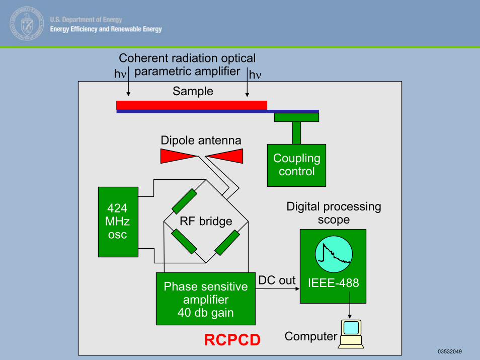
RCPCD
RF bridgeDigital processing
scope
IEEE-488
Sample
424MHzosc
DC out
hνhν
Computer
Dipole antenna
Coherent radiation optical parametric amplifier
Phase sensitiveamplifier
40 db gain
Couplingcontrol
03532049
Time-resolved Photoluminescence and Lifetime Measurements
Time-resolved Photoluminescence and Lifetime Measurements
03532050

Time-resolved PhotoluminescenceTime-resolved Photoluminescence
• Inject excess carriers into a sample with laser causing photoluminescence
• Watch the photoluminescence intensity decay
• Use a semiconductor diode, single photon counting, up-conversion TRPL
03532051
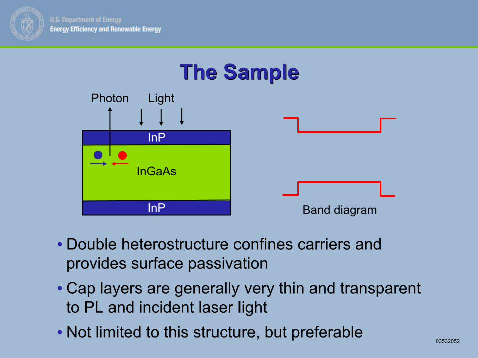
The SampleThe Sample
• Double heterostructure confines carriers and provides surface passivation
• Cap layers are generally very thin and transparent to PL and incident laser light
• Not limited to this structure, but preferable
Band diagram
InP
InGaAs
InP
Light
03532052
Photon
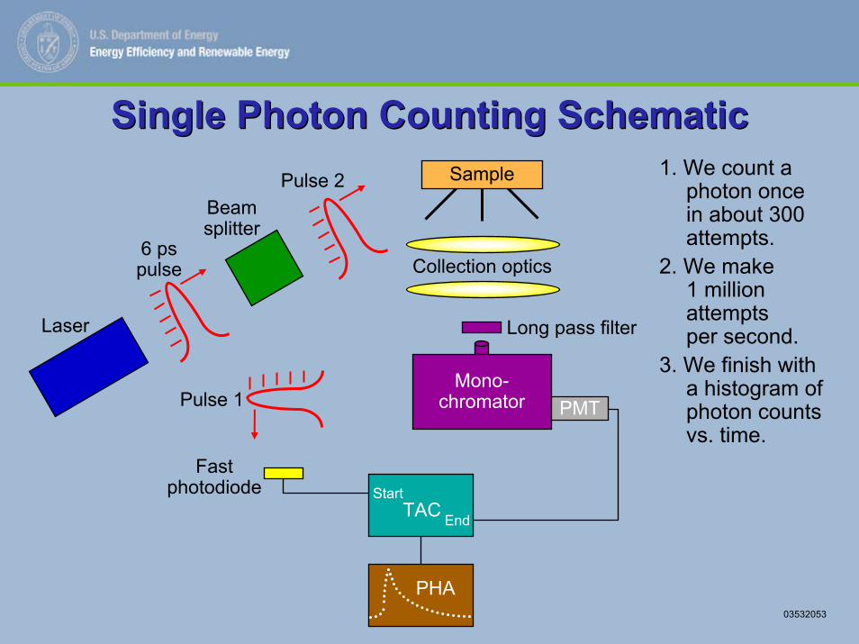
Single Photon Counting SchematicSingle Photon Counting Schematic1. We count a
photon once in about 300 attempts.
2. We make 1 million attempts per second.
3. We finish with a histogram of photon counts vs. time.
Collection optics
Laser
6 pspulse
Beamsplitter
Pulse 2 Sample
Long pass filter
Mono-chromator PMT
Start
EndTAC
PHA
Fastphotodiode
Pulse 1
03532053

ResultsResultsNational Renewable Energy LaboratoryElectro-Optical Characterization GroupWyatt Metzger (303) 384-6572 Expon. Decay Constant = 1.22e-06 (s)
1086420µ (s)
103
102
101
100
Cou
nts
Expon. decay constant = 1.22e-06 (s)
03532054

Lifetime often Correlated with VocLifetime often Correlated with Voc
0.85
0.80
0.75
0.70
0.65
0.60
0.55
V oc(V
)
0.1 1Lifetime (ns)
CdTe – JAP 94 (5): 3549-3555, Sep. 1, 2003CIGS – Proceedings of the 29th IEEE pp.511–514, 2002CIGS – JAP 94 (9): 5584–5591, Nov. 1, 2003CIGS – APL 73(9): 1224-1226, 1998CIGS – Thin Solid Films 387: 262-267, 2001GaInAs – 3rd World Conference on Photovoltaic Energy Conversion 2003GaNP - J. Cryst. Growth 259 (3): 223–231, 2003
03532055

The Experimental Range The Experimental Range
1 100 10000 1E+06 1E+08 1E+10 1E+12 1E+14Lifetime range (fs)
Up-conversion
TRPL
RCPCD
Good for wavelengthsup to 1.4 um
03532056

Lifetime Ranges for Different MaterialsLifetime Ranges for Different MaterialsMaterial Lifetime Range Mechanism Injection Control
GaAs
GaInAs
GaInP
CdTe 200 ps - 2ns nonradiative no some
CIGS
GaNP
GaInAsN
GaAsN
GaInN
Radiative, SRH yes yesShort - 22 µs
100 fs - 10 µs
200 ps - 25 ns
300 ps - 3 ns
100 ps - 10 ns
100 ps - 10 ns
100 ps - 10 ns
Auger, Radiative, SRH
yes yes
Mostly SRH no some
100 ps - 10 ns
nonradiative no not monitored
nonradiative no Depends on N
nonradiative no Depends on N
nonradiative no Depends on N
nonradiative no Depends on N03532057

Liquidnitrogen
dewar
Laser for option of
optical DLTS
Temperaturecontroller
DLTS unit
Oscilloscopeto view signal
Deep Level Transient SpectroscopyDeep Level Transient Spectroscopy
03532058

The Effects of Traps (Impurities)The Effects of Traps (Impurities)n-Type
p-Type
Trap (impurity) Trap (impurity)
Depleted region
Example: gold in silicon03532059

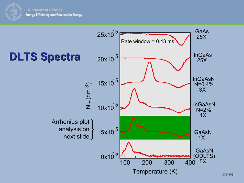
25x1015
20x1015
15x1015
10x1015
5x10¹⁵
0x1015
NT
(cm
-3)
300200100Temperature (K)
Rate window = 0.43 ms
GaAs25X
InGaAs25X
InGaAsNN=0.4%
3X
InGaAsNN=2%
1X
GaAsN1X
GaAsN(ODLTS)
5X
Arrhenius plotanalysis on
next slide
400
03532061
DLTS SpectraDLTS Spectra

62
60
58
56
54
52
50
ln( t
*vth
NV)
98765431000/T (K )-1
0.30 0.20 0.18 0.16 0.14 0.12Temperature (K)
Ea(eV) s (cm2 ) NT(cm-3)
0.18 2x10-16 1.1x10¹⁶
0.25 6x10-16 2.8x10¹⁵
0.70 1x10-13 2.0x10¹⁵
03532062

Concentration of Traps Corresponding with the Low-T Peak Increases with Increasing Amounts of N
Concentration of Traps Corresponding with the Low-T Peak Increases with Increasing Amounts of N
20x1015
15
10
5
0
NT
170160150140130120110Temperature (K)
MF057MF058MF152MF153MF166Peak1Peak2fit MF057
Rate window = 5 msFilling pulse width = 1 s The defect
correspondingto this peak maybe responsible for the low Vocand poor solarcell performanceof InGaAsN.
03532063

Drive Level Capacitance ProfilingDrive Level Capacitance Profiling
Hg probeHg probe
Sample
LockLock--in amplifierin amplifier
AC supply
DC supply
Computer
I to VI to Vconverterconverter
03532064
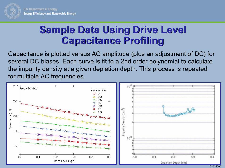
Sample Data Using Drive Level Capacitance Profiling
Sample Data Using Drive Level Capacitance Profiling
Capacitance is plotted versus AC amplitude (plus an adjustment of DC) for several DC biases. Each curve is fit to a 2nd order polynomial to calculate the impurity density at a given depletion depth. This process is repeated for multiple AC frequencies.
03532065

Temperature Dependent Current-VoltageTemperature Dependent Current-Voltage
Liquidnitrogendewar
Samplechamber
77 K
Temperaturecontroller
High resolutionelectrometer
Pump
Computer
03532066

Sample Temperature Dependent IV DataSample Temperature Dependent IV DataCurrent-Voltage measurements are taken as a sample is cooled down to liquid nitrogen temperature. The current density is then plotted in an Arrhenius plot for several reverse biases. The slope of this data can provide activation energies or insight into band diagram information.
-25
-20
-15
-10
12108641000/T (K-1)
In (J
)
03532067

Energy Resolved PhotoluminescenceEnergy Resolved Photoluminescence• Energy resolved photoluminescence is a process that helps researchers determine the bandgap for a semiconductor material and also enables researchers to look for defects within those kinds of materials. The fewer defects a material has the more efficiently it will perform. Photoluminescence is the product of electron hole pairs recombining and producing photons. Those photons are emitted from within the bandgap and below the bandgap if there are defects.
• The experiment set up is very simple and straightforward. Collimated light (laser) is focused onto a semiconductor sample to excite the electrons above the bandgap. Many laser lines can be used. At NREL there are six CW laser lines available and they range between 325nm to 822nm. The photoluminescence is then collected through a lens collimated and focused onto a slit on an imaging spectrograph. This light is then passed through the spectrograph to either a CCD array or a photodiode array. The spectra is then acquired and recorded through data acquisition software onto a computer. It can then be analyzed and archived.
03532068

ERPL Measurement Using Continuous Flow (portable) Cryostat
ERPL Measurement Using Continuous Flow (portable) Cryostat
03532069

ERPL CapabilitiesERPL Capabilities• CCD (charge coupled device) Camera for PL measurements in the visible
• InGaAs PDA (photodiode array) for measurements in the NIR
• Imaging spectrometer with four gratings for use with the CCD and PDA
• InSb detector with a scanning monochrometer for measurements in the IR
• Ge detector with a triple grating monochrometer for high resolution measurements at longer wavelengths.
• Closed cycle cryostat which enables measurements to be performed at 4.25 K
• Temperature controller to allow temperature dependent measurements.
• Continuous flow cryostats that are portable and can be used with different setups in the laboratory (technique development)
03532070
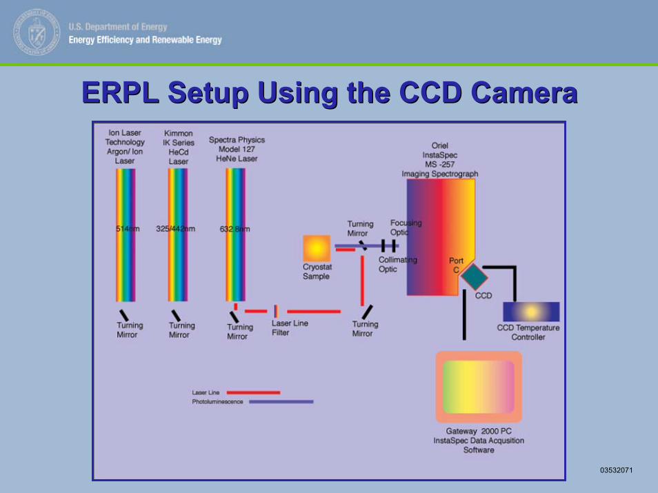
ERPL Setup Using the CCD CameraERPL Setup Using the CCD Camera
03532071

15x103
10
5
0
ND
cor
rect
ed d
ata
920900880860840820800780760Wavelength (nm)
Sample K98G2-13cnts_308 19 mWcnts_303 1 mWcnts_304 2 mWcnts_305 5 mWcnts_306 10 mWcnts_307 15 mW
PL Spectra of CdTe Film at 4.25KPL Spectra of CdTe Film at 4.25K
03532072

PL Spectra of CIS/CGS Material at Room Temperature
PL Spectra of CIS/CGS Material at Room Temperature
600
500
400
300
200
100
0
ND
cor
rect
ed d
ata
1300120011001000900800700Wavelength (nm)
700
03532073

• Reflectance, transmittance, and absorption measurements• Spectral region is home to molecular and free carrier absorption• Impurity analysis• Bonding configurations• Quantitative analysis• Nondestructive• Sensitivity advantages over dispersive systems• Imaging capabilities• Low-gap photoluminescence measurements and mapping
Fourier Transform Infrared (FTIR) Spectroscopy
Brian M. Keyes and Lynn M. Gedvilas
Fourier Transform Infrared (FTIR) Spectroscopy
Brian M. Keyes and Lynn M. Gedvilas
03532074

Impurity Concentrations in Crystalline SiliconImpurity Concentrations in Crystalline Silicon
0.6
1.0
1.4
1.8
2.2
2.6
6008001000120014001600Wavenumbers (cm-1)
Interstitial oxygen
Substitutionalcarbon
Si-O stretch
• Impurity content and process control• Oxygen precipitates — related to material quality• Study of SiNx and SiCx layers
Abs
orba
nce
03532075

Amorphous-Microcrystalline Silicon Transition
Amorphous-Microcrystalline Silicon Transition
• Si-H infrared bonding configurations are related to microcrystallinity• Higher crystalline volume fractions favor increased oxidation — measure of device quality
H945-1 H2/SiH4 = 10H955-1 H2/SiH4 = 0H948-1 H2/SiH4 = 2
0
400
800
1200
1600
100015002000
Si-H stretch
Si-O modes
Si-H2bending
Si-H wag
500
2000
Wavenumbers (cm-1)
Abs
orba
nce
03532076
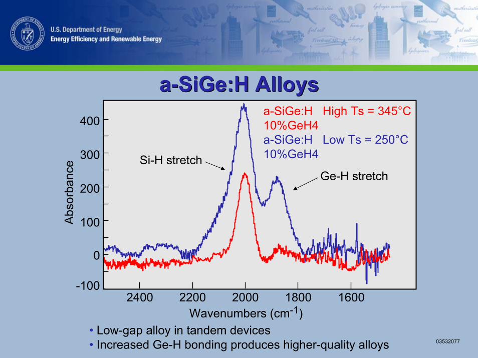
a-SiGe:H Alloysa-SiGe:H Alloys
• Low-gap alloy in tandem devices• Increased Ge-H bonding produces higher-quality alloys
a-SiGe:H High Ts = 345°C 10%GeH4a-SiGe:H Low Ts = 250°C 10%GeH4
0
100
200
300
400
16001800200022002400
Si-H stretchGe-H stretch
-100
Wavenumbers (cm-1)
Abs
orba
nce
03532077

Transparent Conducting
Oxide Films —Uniformity Map
Transparent Conducting
Oxide Films —Uniformity Map•Support of combinatorial growth efforts
•Reflectance and transmittance maps
•Nondestructive measure of transport properties through determination of plasma frequency
55
-40
-20
0
20
40
40200-20-40Position (mm)
Pos
ition
(mm
)
03532078

Variable Angle Spectroscopic EllipsometerVariable Angle Spectroscopic Ellipsometer• Rotating compensator ellipsometer• Automated variable angle measurement• Sample translation and mapping• Small-spot focusing ability (~1 mm spot size)• Dual array detectors, 0.7–5.0 eV range, spectra in a few seconds
Collection opticsfiber-coupled
to remotespectrometers
Dual light sourceUV – NIR
Optical fibers
Stepping-motor driven rotation stages —for sample and collection optics arm
Sample x, y translation stages
Sample (Si wafer)
03532079
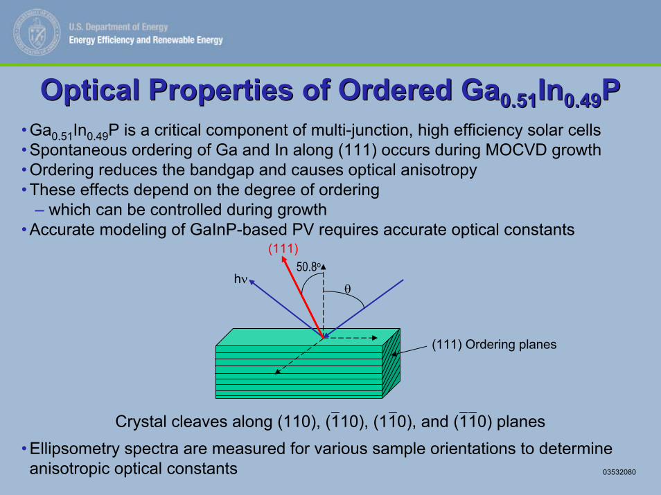
Optical Properties of Ordered Ga0.51In0.49POptical Properties of Ordered Ga0.51In0.49P• Ga0.51In0.49P is a critical component of multi-junction, high efficiency solar cells• Spontaneous ordering of Ga and In along (111) occurs during MOCVD growth• Ordering reduces the bandgap and causes optical anisotropy• These effects depend on the degree of ordering
– which can be controlled during growth• Accurate modeling of GaInP-based PV requires accurate optical constants
• Ellipsometry spectra are measured for various sample orientations to determine anisotropic optical constants
Crystal cleaves along (110), (110), (110), and (110) planes
(111) Ordering planes
θhν
50.8o
(111)
03532080

Ga0.51In0.49P Optical Properties vs. OrderingGa0.51In0.49P Optical Properties vs. Ordering
•Degree of ordering expressed in terms of ordering parameter h, 0 < h < 1•In figures above, red corresponds to h = 0.45, green h = 0.31, and blue h = 0.10
•Extraordinary optical constants, on left side, show splitting of valence band max due to reduced symmetry produced by ordering
•Ordinary optical constants on right side shows reduced band gap with ordering
03532081
me969_e8me956_e3me972_e5
me969_o8me956_o3me972_o5
e-Axis Optical Constants
Photon energy (eV)1.60 1.70 1.80 1.90 2.00 2.10
0.00
0.05
0.10
0.15
Extin
ctio
n co
effic
ient
‘k’
o-Axis Optical Constants
Photon energy (eV)1.60 1.70 1.80 1.90 2.00 2.10
0.00
0.05
0.10
0.15
Extin
ctio
n co
effic
ient
‘k’

In-situ Real Time Spectroscopic Ellipsometry Studies of a-Si:H Growth
In-situ Real Time Spectroscopic Ellipsometry Studies of a-Si:H Growth
•NREL silicon materials team currently working to optimize HIT (heterojunction with intrinsic layer) solar cells
•Devices require very thin amorphous silicon layers on silicon substrate•Efficiencies as high as 21% have been achieved — because of very effective surface passivation by a-Si:H layer on silicon wafer
•Accurate thickness control requires real-time feedback — growth rates change with filament aging and changes in deposition gas flow rates, etc.
•Passivation requires immediate a-Si:H deposition at interface — epitaxialdeposition on wafer surface hinders passivation effect of a-Si:H — c-Siinterface
n-Type silicon wafern-Type silicon wafer
50 A undoped a-Si:H100–300 Å p-type a-Si:H
03532082

In-Situ RTSE Provides Real-time Feedback andPost-deposition Analysis of Crystallinity
In-Situ RTSE Provides Real-time Feedback andPost-deposition Analysis of Crystallinity
020
40
60
80
100
120
0 8 16 24 32 40 48 56 64
EMA %
i-Layer thickness (Å)
050
100
150
200
250
300
0 20 40 60 80 100
i-Layerthickness
n-Layerthickness
Time (sec)
03532083
a-Si:H
C-Si
Thic
knes
s (Å
)
EM
A %
of n
c
Related Documents