ELCT 371: Electronics Pre-Req: CSCE 211, ELCT 222 Dr. Goutam Koley Room 3A12, 777- 3469, [email protected] Lecture Hours: Tue & Thurs 12.30 – 1:45 AM SWGN 2A15 Office Hours: Tue and Thurs 2.30 – 3.30, and by appointment 1

ELCT 371: Electronics Pre-Req: CSCE 211, ELCT 222 Dr. Goutam Koley Room 3A12, 777- 3469, [email protected]@engr.sc.edu Lecture Hours: Tue & Thurs.
Jan 04, 2016
Welcome message from author
This document is posted to help you gain knowledge. Please leave a comment to let me know what you think about it! Share it to your friends and learn new things together.
Transcript
ELCT 371: ElectronicsPre-Req: CSCE 211, ELCT 222 Dr. Goutam Koley
Room 3A12, 777- 3469, [email protected]
Lecture Hours: Tue & Thurs 12.30 – 1:45 AMSWGN 2A15
Office Hours: Tue and Thurs 2.30 – 3.30, and by appointment
1
Objective
Objective: To learn the basics of analog circuit design and analysis
Text book: Electronics, by Allan R. Hambley, 2nd Edition, Prentice Hall, Upper Saddle River, NJ 07458, 2000ISBN # 0136919820
2
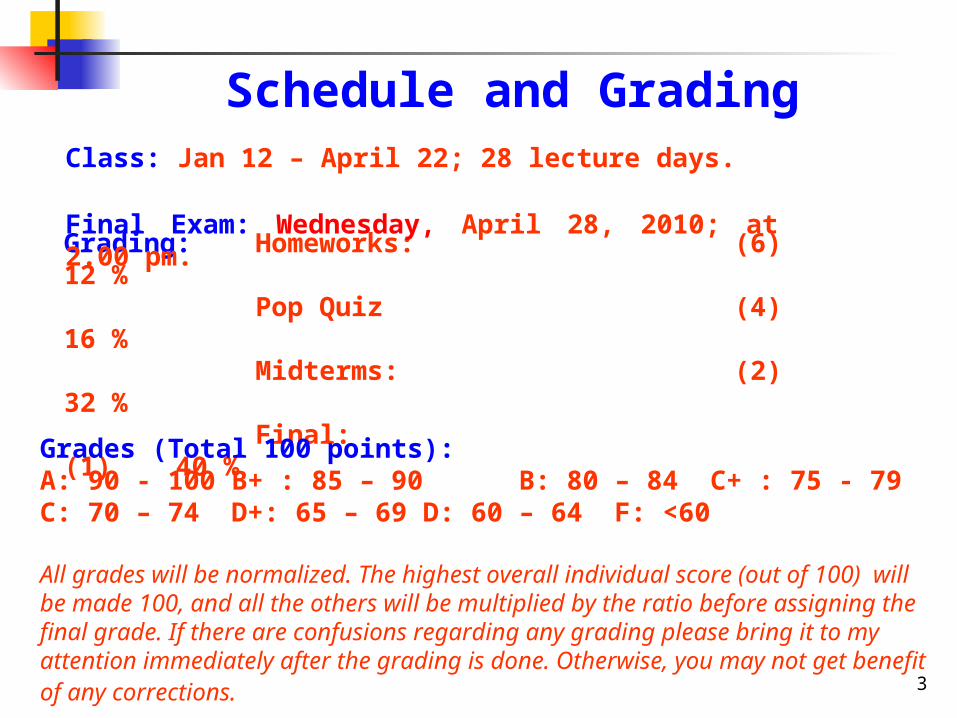
Schedule and Grading
Grading: Homeworks: (6) 12 %Pop Quiz (4) 16 %Midterms: (2) 32 %Final: (1) 40 %
Class: Jan 12 – April 22; 28 lecture days.
Final Exam: Wednesday, April 28, 2010; at 2.00 pm.
Grades (Total 100 points):A: 90 - 100 B+ : 85 – 90 B: 80 – 84 C+ : 75 - 79C: 70 – 74 D+: 65 – 69 D: 60 – 64 F: <60
All grades will be normalized. The highest overall individual score (out of 100) will be made 100, and all the others will be multiplied by the ratio before assigning the final grade. If there are confusions regarding any grading please bring it to my attention immediately after the grading is done. Otherwise, you may not get benefit of any corrections. 3

Some reminders…
Eating or drinking in class is NOT preferable. However, if you absolutely have to, you must not disturb others.
Do not enter the class if you are more than 15 minutes late, without very valid reasons
No retake of exams/tests permitted unless you let me know prior to the test/exam and have valid reasons
PLEASE ADHERE TO THE UNIVERSITY OF SOUTH CAROLINA HONOR CODE (No cheating in any form!!!)
4
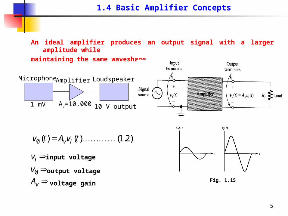
An ideal amplifier produces an output signal with a larger amplitude while
maintaining the same waveshape
1.4 Basic Amplifier Concepts
)2.1()()(0 tvAtv iv
iv input voltage
0v output voltage
vA voltage gain
Microphone
1 mV
Amplifier
Av=10,000
Loudspeaker
10 V output
Fig. 1.15
5
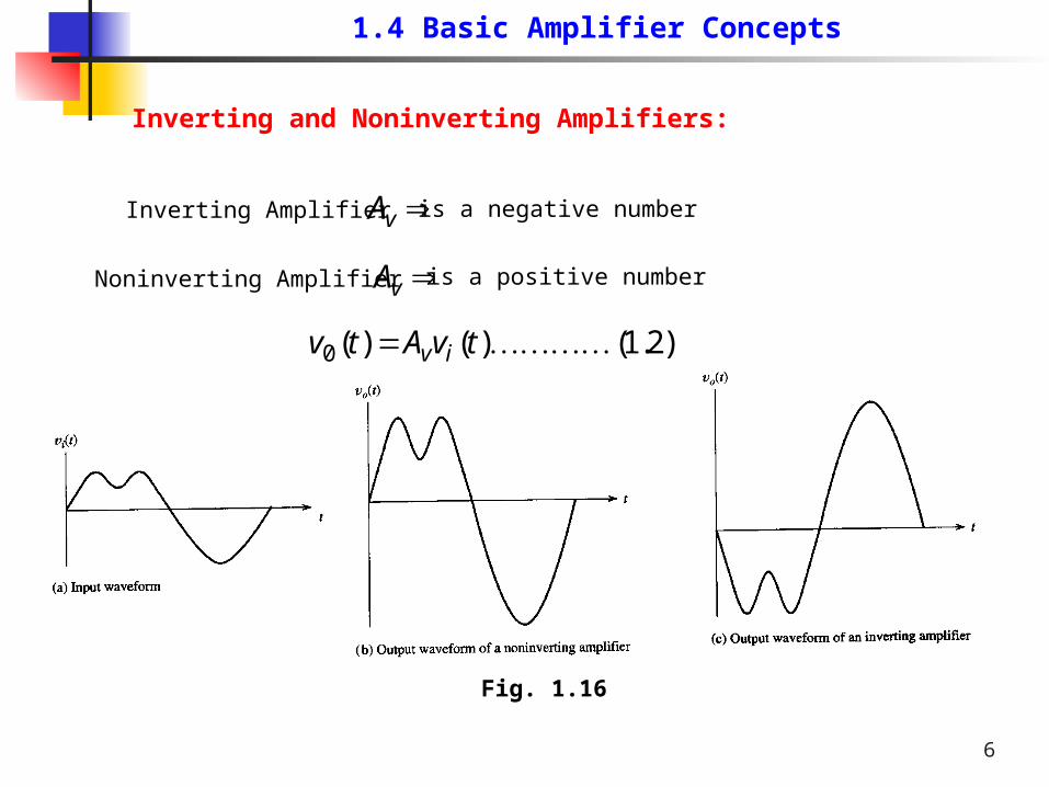
Inverting and Noninverting Amplifiers:
1.4 Basic Amplifier Concepts
)2.1()()(0 tvAtv iv
vAInverting Amplifier is a negative number
Noninverting Amplifier vA is a positive number
Fig. 1.16
6
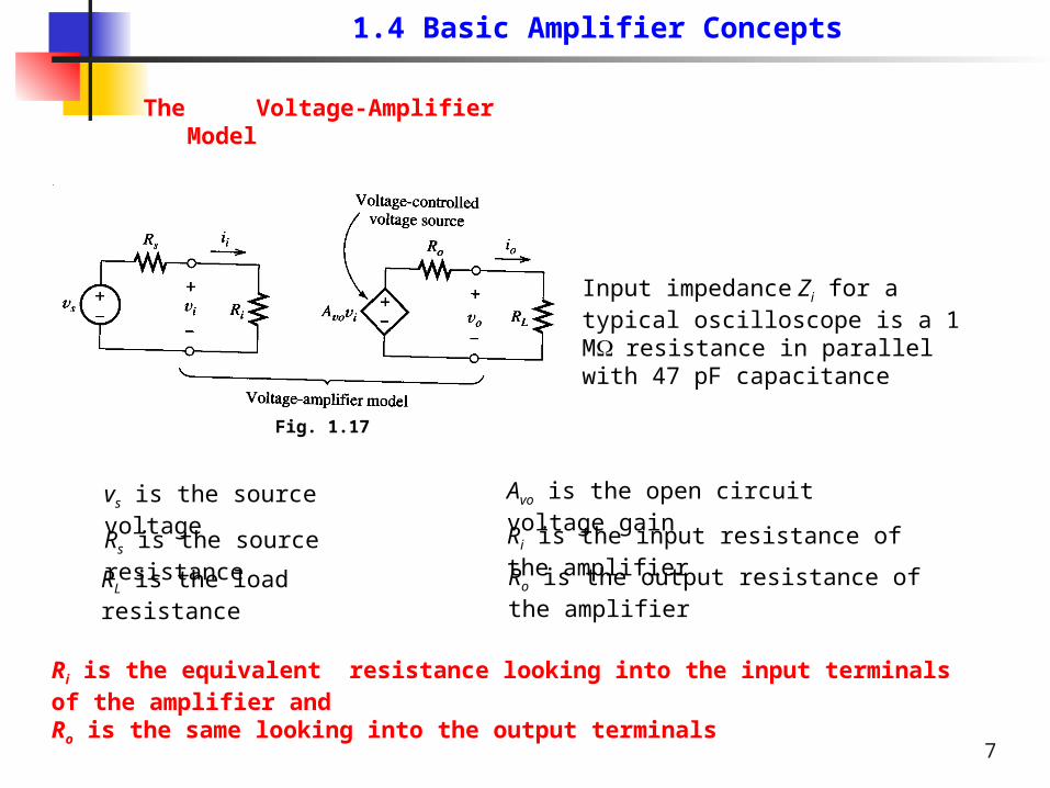
The Voltage-Amplifier Model
1.4 Basic Amplifier Concepts
Fig. 1.17
vs is the source voltage
Rs is the source resistance
RL is the load resistance Ro is the output resistance of the amplifier
Ri is the input resistance of the amplifier
Ri is the equivalent resistance looking into the input terminals of the amplifier andRo is the same looking into the output terminals
Input impedance Zi for a typical oscilloscope is a 1 Mresistance in parallel with 47 pF capacitance
Avo is the open circuit voltage gain
7
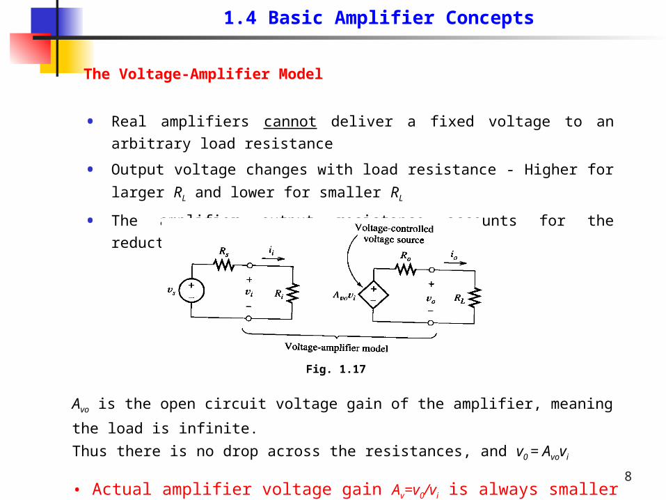
The Voltage-Amplifier Model
• Real amplifiers cannot deliver a fixed voltage to an arbitrary load resistance
• Output voltage changes with load resistance - Higher for larger RL and lower
for smaller RL
• The amplifier output resistance accounts for the reduction in output voltage
1.4 Basic Amplifier Concepts
Avo is the open circuit voltage gain of the amplifier, meaning the load is infinite.
Thus there is no drop across the resistances, and v0 = Avovi
• Actual amplifier voltage gain Av=v0/vi is always smaller than Avo
Fig. 1.17
8

1.4 Basic Amplifier Concepts
Fig. 1.17
ii i
iA 0
Current Gain
L
iv
ii
L
ii R
RA
Rv
Rv
i
iA
/
/00
iv v
vA 0
is the voltage gain with the loadresistor connected. Note that Av is
smaller than Av0
9
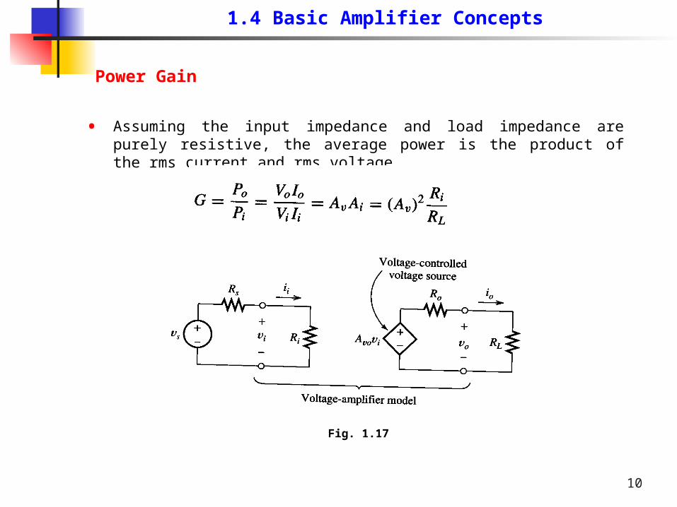
Power Gain
• Assuming the input impedance and load impedance are purely resistive, the average power is the product of the rms current and rms voltage.
1.4 Basic Amplifier Concepts
Fig. 1.17
10

Example 1.1: Find voltage gain, current gain, and power gain for the circuit below
1.4 Basic Amplifier Concepts
11
Fig. 1.18

1.5 Cascaded Amplifiers
Fig. 1.19
12
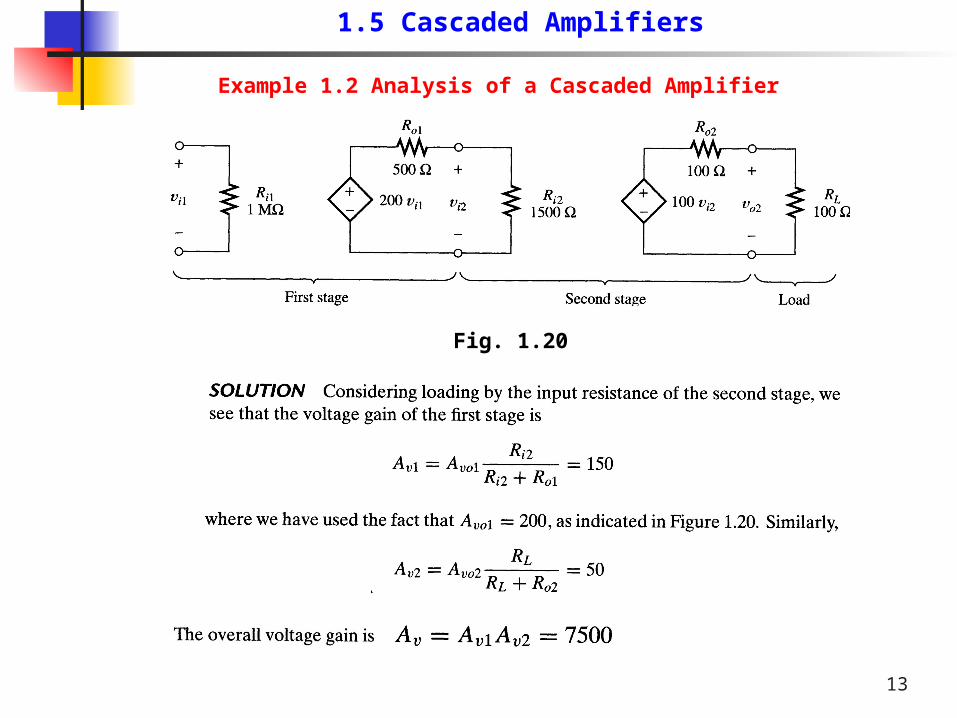
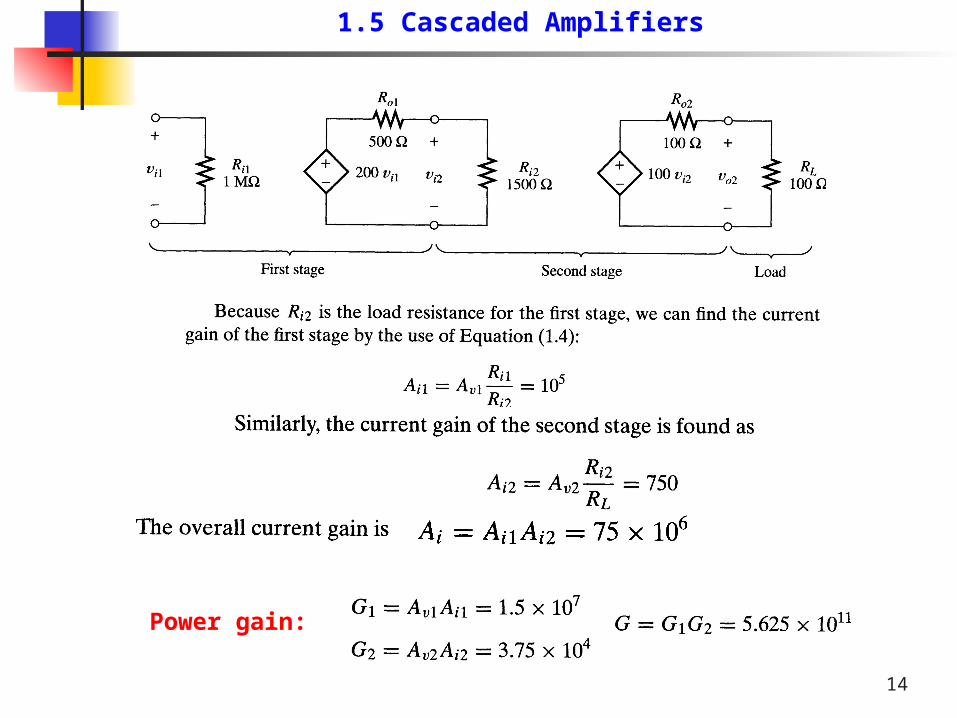
1.5 Cascaded Amplifiers
Fig. 1.20
Example 1.2 Analysis of a Cascaded Amplifier
13
1.5 Cascaded Amplifiers
14
Power gain:

Simplified Models for Cascaded Amplifier Stages
Example 1.3 Determining the Overall Model of a Cascaded Amplifier
Fig. 1.20
1.5 Cascaded Amplifiers
15

Fig. 1.21 Simplified model for the cascaded amplifiers of Fig. 1.20
1.5 Cascaded Amplifiers
Question: Who provides the power to amplify the input signal?
16
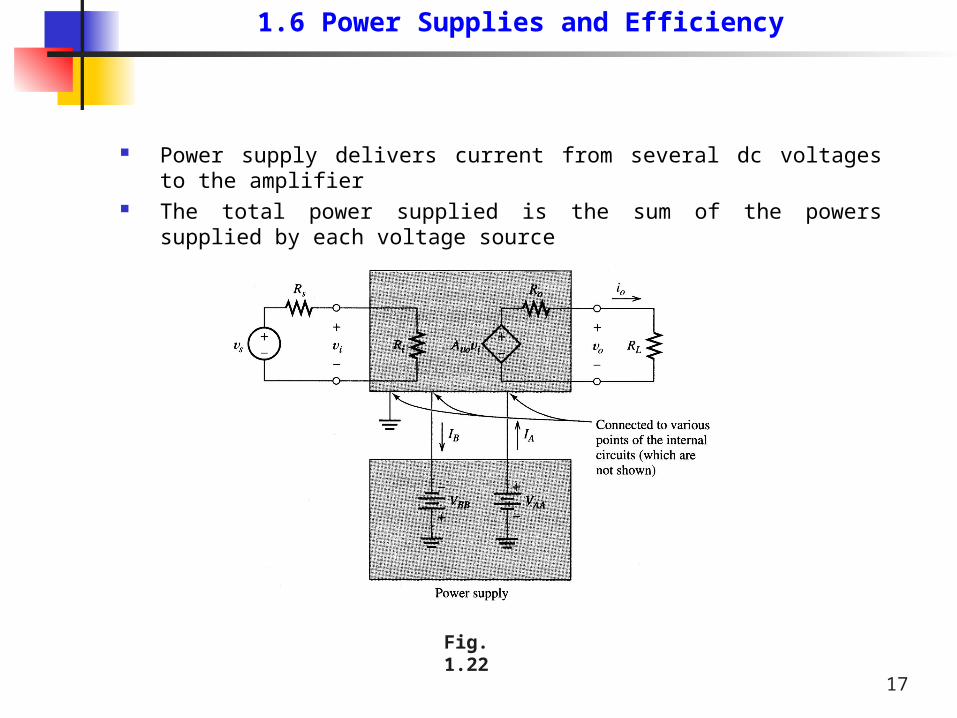
Power supply delivers current from several dc voltages to the amplifier The total power supplied is the sum of the powers supplied by each voltage
source
1.6 Power Supplies and Efficiency
Fig. 1.22
17

Fig. 1.23
Here, Pi = power entering the amplifier from the signal source
Ps = power from the power supply
P0 = output power
Pd = dissipated power
1.6 Power Supplies and Efficiency
18
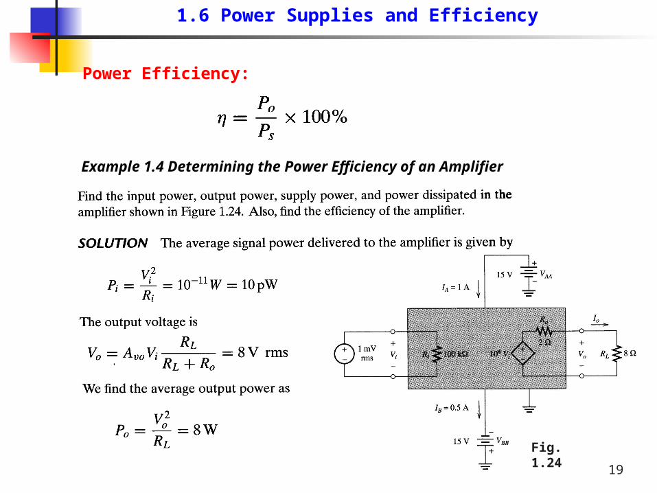
Power Efficiency:
Example 1.4 Determining the Power Efficiency of an Amplifier
Fig. 1.24
1.6 Power Supplies and Efficiency
19

Fig. 1.24
1.6 Power Supplies and Efficiency
20
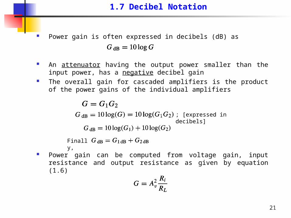
Power gain is often expressed in decibels (dB) as
An attenuator having the output power smaller than the input power, has a negative decibel gain
The overall gain for cascaded amplifiers is the product of the power gains of the individual amplifiers
Power gain can be computed from voltage gain, input resistance and output resistance as given by equation (1.6)
1.7 Decibel Notation
; [expressed in decibels]
Finally,
21
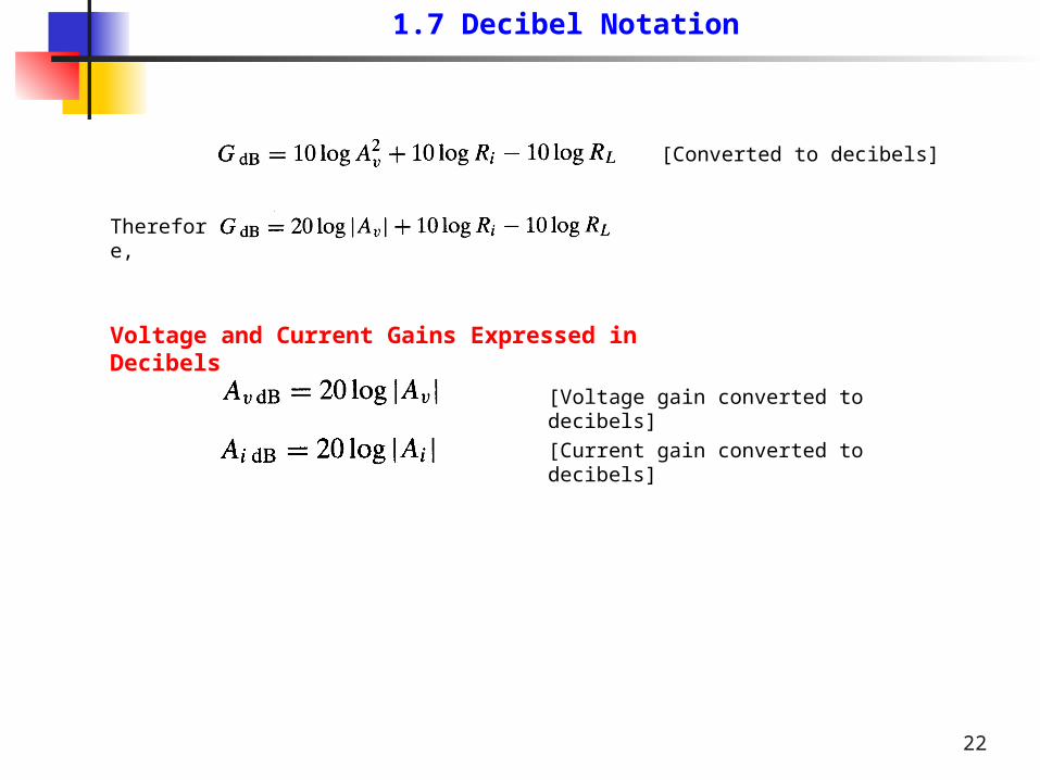
[Converted to decibels]
Therefore,
Voltage and Current Gains Expressed in Decibels
[Voltage gain converted to decibels]
[Current gain converted to decibels]
1.7 Decibel Notation
22
Related Documents