1 A R E P O R T ON Efficient Floating Point 32-bit single Precision Multipliers Design using VHDL Under the guidance of Dr. Raj Singh, Group Leader, VLSI Group, CEERI, Pilani. By Raj Kumar Singh Parihar 2002A3PS013 Shivananda Reddy 2002A3PS107 BIRLA INSTITUTE OF TECHNOLOGY AND SCIENCE PILANI – 333031 May 2005

Welcome message from author
This document is posted to help you gain knowledge. Please leave a comment to let me know what you think about it! Share it to your friends and learn new things together.
Transcript

1
A R E P O R T
ON
Efficient Floating Point 32-bit single Precision
Multipliers Design using VHDL
Under the guidance ofDr. Raj Singh,
Group Leader, VLSI Group, CEERI, Pilani.
By
Raj Kumar Singh Parihar 2002A3PS013Shivananda Reddy 2002A3PS107
BIRLA INSTITUTE OF TECHNOLOGY AND SCIENCEPILANI – 333031
May 2005

2
A R E P O R T
ON
Efficient Floating Point 32-bit single Precision
Multipliers Design using VHDL
Under the guidance of
Dr. Raj Singh, Group Leader, VLSI Group, CEERI, Pilani.
By
Raj Kumar Singh Parihar 2002A3PS013Shivananda Reddy 2002A3PS107
B.E. (Hons) Electrical and Electronics Engineering
Towards the partial fulfillment of the course BITS C335,Computer Oriented Project
BIRLA INSTITUTE OF TECHNOLOGY AND SCIENCEPILANI – 333031
May 2005

3
ACKNOWLEDGEMENTS
We are thankful to our project instructor, Dr. Raj Singh, Scientist, IC Design Group,
CEERI, Pilani for giving us this wonderful opportunity to do a project under his
guidance. The love and faith that he showered on us have helped us to go on and
complete this project.
We would also like to thank Dr. Chandra shekhar, Director, CEERI, PIlani, Dr. S. C.
Bose and all other members of IC Design Group, CEERI, for their constant support. It
was due to their help that we were able to access books, reports of previous year students
and other reference materials.
We also extend our sincere gratitude to Prof. (Dr.) Anu Gupta, EEE, Prof. (Dr.) S.
Gurunarayanan, Group Leader, Instrumentation group and Mr. Pawan Sharma, In-charge,
Oyster Lab, for allowing us to use VLSI CAD facility for analysis and simulation of the
designs.
We also thank to Mr. Manish Saxena (T.A., BITS, Pilani), Mr. Vishal Gupta, Mr. Vishal
Malik, Mr. Bhoopendra singh and the Oyster lab operator Mr. Prakash Kumar for their
Guidance, support, help and encouragement.
In the end, we would like to thank our friends, our parents and that invisible force that
provided moral support and spiritual strength, which helped us completing this project
successfully.

4
BIRLA INSTITUTE OF TECHNOLOGY AND SCIENCE
PILANI (Rajasthan) – 333031
CERTIFICATE
This is to certify that the project entitled “Efficient Floating Point
Multipliers: Design & Simulation using VHDL” is the bonafide work of Raj
Kumar Singh (2002A3PS013) done in the second semester of the academic
year 2004-2005. He has duly completed his project and has fulfilled all the
requirements of the course BITS C313, Lab Oriented Project, to my
satisfaction.
Dr. Raj Singh
Scientist, IC Design Group
CEERI, Pilani – RAJ.
Date:

5
BIRLA INSTITUTE OF TECHNOLOGY AND SCIENCE
PILANI (Rajasthan) – 333031
CERTIFICATE
This is to certify that the project entitled “Efficient Floating Point
Multipliers: Design & Simulation using VHDL” is the bonafide work of
Shivananda Reddy (2002A3PS107) done in the second semester of the
academic year 2004-2005. He has duly completed his project and has
fulfilled all the requirements of the course BITS C313, Lab Oriented Project,
to my satisfaction.
Dr. Raj Singh
Scientist, IC Design Group
CEERI, Pilani – RAJ.
Date:

6
ABSTRACT
These Lab-Oriented Project and Activities have been carried out into two parts. First Half
is the Floating Point Representation Using IEEE-754 Format (32 Bit Single Precision)
and second Half is simulation, synthesis of Design using HDLs and Software Tools.The
Binary representation of decimal floating-point numbers permits an efficient
implementation of the proposed radix independent IEEE standard for floating-point
arithmetic. 2’s Complement Scheme has been used throughout the project.
A Binary multiplier is an integral part of the arithmetic logic unit (ALU) subsystem found
in many processors. Integer multiplication can be inefficient and costly, in time and
hardware, depending on the representation of signed numbers. Booth's algorithm and
others like Wallace-Tree suggest techniques for multiplying signed numbers that works
equally well for both negative and positive multipliers. In this project, we have used
VHDL as a HDL and Mentor Graphics Tools (MODEL-SIM & Leonardo Spectrum) for
describing and verifying a hardware design based on Booth's and some other efficient
algorithms. Timing and correctness properties were verified. Instead of writing Test-
Benches & Test-Cases we used Wave-Form Analyzer which can give a better
understanding of Signals & variables and also proved a good choice for simulation of
design. Hardware Implementations and synthesizability has been checked by Leonardo
Spectrum and Precision Synthesis.
Key terms: IEEE-754 Format, Simulation, Synthesis, Slack, Signals & Variables,
HDLs.
7
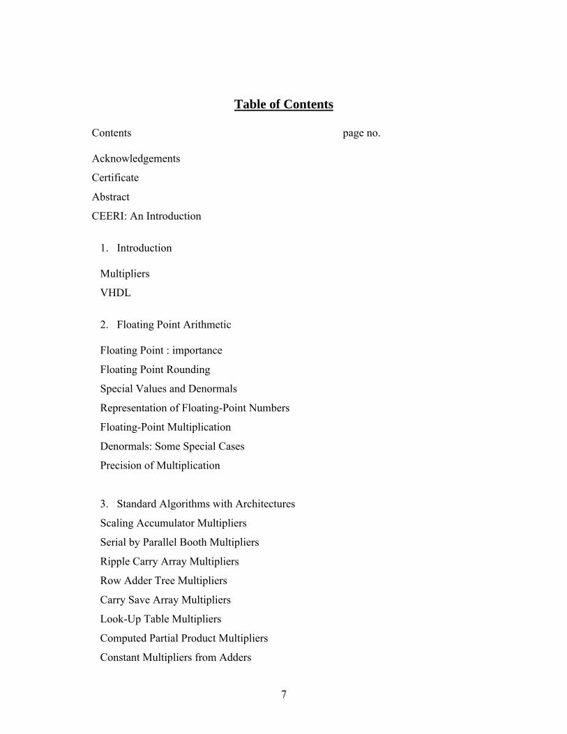
Table of Contents
Contents page no.
Acknowledgements
Certificate
Abstract
CEERI: An Introduction
1. Introduction
Multipliers
VHDL
2. Floating Point Arithmetic
Floating Point : importance
Floating Point Rounding
Special Values and Denormals
Representation of Floating-Point Numbers
Floating-Point Multiplication
Denormals: Some Special Cases
Precision of Multiplication
3. Standard Algorithms with Architectures
Scaling Accumulator Multipliers
Serial by Parallel Booth Multipliers
Ripple Carry Array Multipliers
Row Adder Tree Multipliers
Carry Save Array Multipliers
Look-Up Table Multipliers
Computed Partial Product Multipliers
Constant Multipliers from Adders

8
Wallace Trees
Partial Product LUT Multipliers
Booth Recoding
4. Simulation, Synthesis & Analysis
4.1. Booth Multiplier
4.1.1. VHDL Code
4.1.2. Simulation
4.1.3. Synthesis
4.1.4. Critical Path of Design
4.1.5. Technology Independent Schematic
4.2 Combinational Multiplier
4.2.1. VHDL Code
4.2.2. Simulation
4.2.3. Synthesis
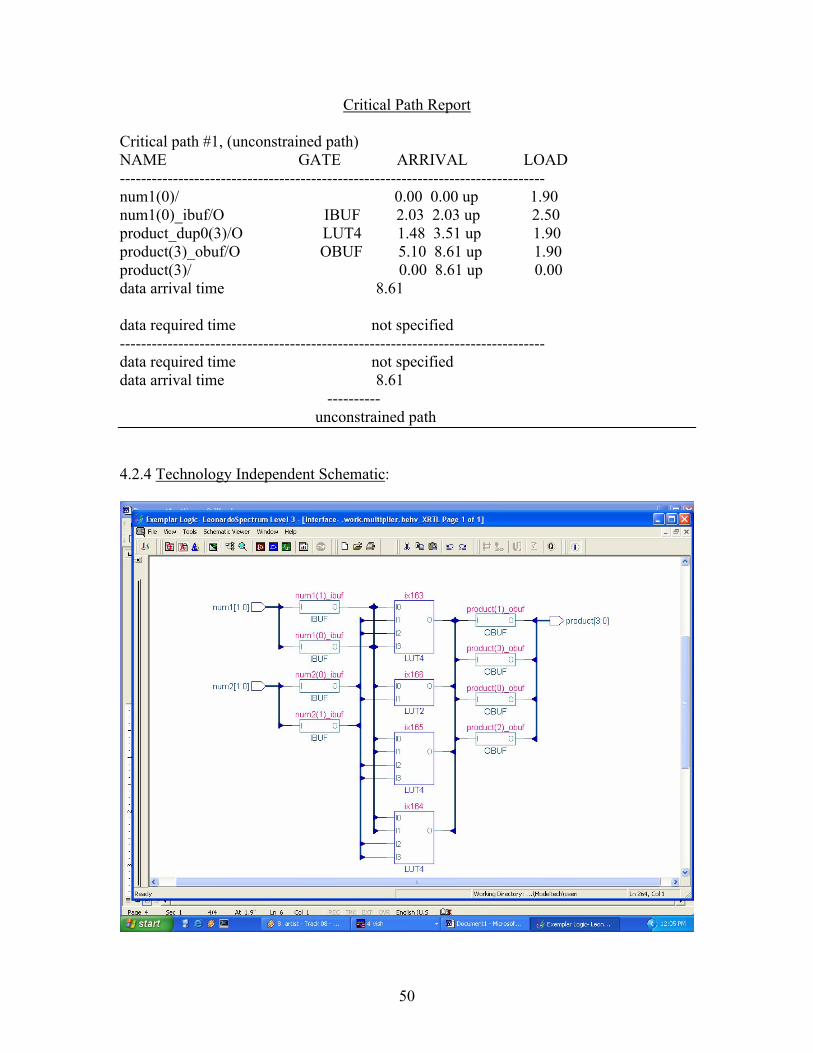
4.2.4. Technology Independent Schematic
4.3 Sequential Multiplier
4.3.1. VHDL & Veri-log Code
4.3.2. Simulation
4.3.3. Synthesis
4.3.4. Technology Independent Schematic
4.3.5. Critical Path of Design
4.4 CSA Wallace-Tree Architecture
4.3.1. VHDL Code
4.3.2. Simulation
4.3.3. Synthesis
4.3.4. Technology Independent Schematic
4.3.5. Critical Path of Design

9
5. New Algorithm
5.1 Multiplication using Recursive –Subtraction
6. Results and Conclusions
7. References

10
CEERI: An Introduction
Central Electronics engineering Research Institute, popularly known as CEERI, is a
constituent establishment of the Council of Scientific and Industrial Research (CSIR),
New Delhi. The foundation stone of the institute was laid on September 21, 1953 by the
then Prime Minister of India, Pt. Jawaharlal Nehru. The actual R&D work started toward
the end of 1958. The institute has blossomed into a center for excellence for the
development of technology and for advanced research in electronics. Over the years the
institute has developed a number of products and processes and has established facilities
to meet the emerging needs of electronics industry.
CEERI, Pilani, since its inception, has been working for the growth of electronics in the
country and has established the required infrastructure and intellectual man power for
undertaking R&D in the following three major areas:
1) Semiconductor Devices
2) Microwave Tubes
3) Electronics Systems
The activities of microwave tubes and semiconductor devices areas are done at Pilani
whereas the activities of electronic systems area are undertaken at Pilani as well as the
two other centers at Delhi and Chennai. The institute has excellent computing facilities
with many Pentium computers and SUN/DEC workstations interlined with internet and e-
mail facilities via VSAT. The institute has well maintained library with an outstanding
collection of books and current journals (and periodicals) published all over the world.
CEERI, with its over 700 highly skilled and dedicated staff members, well-equipped
laboratories and supporting infrastructure is ever enthusiastic to take up the challenging
tasks of research and development in various areas.

11
1. INTRODUCTION
Although computer arithmetic is sometimes viewed as a specialized part of CPU
design, still the discrete component designing is also a very important aspect. A
tremendous variety of algorithms have been proposed for use in floating-point systems.
Actual implementations are usually based on refinements and variations of the few basic
algorithms presented here. In addition to choosing algorithms for addition, subtraction,
multiplication, and division, the computer architect must make other choices. What
precisions should be implemented? How should exceptions be handled? This report will
give the background for making these and other decisions.
Our discussion of floating point will focus almost exclusively on the IEEE
floating-point standard (IEEE 754) because of its rapidly increasing acceptance.
Although floating-point arithmetic involves manipulating exponents and shifting
fractions, the bulk of the time in floating-point operations is spent operating on fractions
using integer algorithms. Thus, after our discussion of floating point, we will take a more
detailed look at efficient algorithms and architectures.
VHDL
The VHSIC (very high speed integrated circuits) Hardware Description Language
(VHDL) was first proposed in 1981. The development of VHDL was originated by IBM,
Texas Instruments, and Inter-metrics in 1983. The result, contributed by many
participating EDA (Electronics Design Automation) groups, was adopted as the IEEE
1076 standard in December 1987.
VHDL is intended to provide a tool that can be used by the digital systems
community to distribute their designs in a standard format. Using VHDL, they are able to
talk to each other about their complex digital circuits in a common language without
difficulties of revealing technical details.
12
As a standard description of digital systems, VHDL is used as input and output to
various simulation, synthesis, and layout tools. The language provides the ability to
describe systems, networks, and components at a very high behavioral level as well as
very low gate level. It also represents a top-down methodology and environment.
Simulations can be carried out at any level from a generally functional analysis to a very
detailed gate-level wave form analysis.
2. FLOATING POINT ARITHMETIC
Many applications require numbers that aren’t integers. There are a number of
ways that non-integers can be represented. Adding two such numbers can be done with
an integer add, whereas multiplication requires some extra shifting. There are various
way to represent the number systems. However, only one non-integer representation has
gained widespread use, and that is floating point.
2.1 Floating Point: Importance
In this system, a computer word is divided into two parts, an exponent and a
significand. As an example, an exponent of ( −3) and significand of 1.5 might represent
the number 1.5 × 2–3 = 0.1875. The advantages of standardizing a particular
representation are obvious.
The semantics of floating-point instructions are not as clear-cut as the semantics
of the rest of the instruction set, and in the past the behavior of floating-point operations
varied considerably from one computer family to the next. The variations involved such
things as the number of bits allocated to the exponent and significand, the range of
exponents, how rounding was carried out, and the actions taken on exceptional conditions
like underflow and over- flow. Now a day computer industry is rapidly converging on the
format specified by IEEE standard 754-1985 (also an international standard, IEC 559).
The advantages of using a standard variant of floating point are similar to those for using
floating point over other non-integer representations. IEEE arithmetic differs from much
previous arithmetic in the following major ways:

13
2.2 Floating Point Rounding:
1. When rounding a “halfway” result to the nearest floating-point number, it picks the one
that is even.
2. It includes the special values NaN, ∞, and −∞.
3. It uses denormal numbers to represent the result of computations whose value is less
than 1.0 × 2Emin.
4. It rounds to nearest by default, but it also has three other rounding modes.
5. It has sophisticated facilities for handling exceptions.
To elaborate on (1), when operating on two floating-point numbers, the result is
usually a number that cannot be exactly represented as another floating- point number.
For example, in a floating-point system using base 10 and two significant digits, 6.1 × 0.5
= 3.05. This needs to be rounded to two digits. Should it be rounded to 3.0 or 3.1? In the
IEEE standard, such halfway cases are rounded to the number whose low-order digit is
even. That is, 3.05 rounds to 3.0, not 3.1.
The standard actually has four rounding modes. The default is round to nearest,
which rounds ties to an even number as just explained. The other modes are round toward
0, round toward +∞, and round toward –∞. We will elaborate on the other differences in
following sections.
2.3 Special Values and Denormals:
Probably the most notable feature of the standard is that by default a computation
continues in the face of exceptional conditions, such as dividing by 0 or taking the square
root of a negative number. For example, the result of taking the square root of a negative
number is a NaN (Not a Number), a bit pattern that does not represent an ordinary
number. As an example of how NaNs might be useful.
Consider the code for a zero finder that takes a function F as an argument and
evaluates F at various points to determine a zero for it. If the zero finders accidentally
yprobe outside the valid values for F, F may well cause an exception. Writing a zero
finder that deals with this case is highly language and operating-system dependent,
because it relies on how the operating system reacts to exceptions and how this reaction

14
is mapped back into the programming language. In IEEE arithmetic it is easy to write a
zero finder that handles this situation and runs on many different systems. After each
evaluation of F, it simply checks to see whether F has returned a NaN; if so, it knows it
has probed outside the domain of F.
In IEEE arithmetic, if the input to an operation is a NaN, the output is NaN (e.g.,
3 + NaN = NaN). Because of this rule, writing floating-point subroutines that can accept
NaN as an argument rarely requires any special case checks.
The final kind of special values in the standard are denormal numbers. In many
floating-point systems, if Emin is the smallest exponent, a number less than 1.0 * 2Emin
cannot be represented, and a floating-point operation that results in a number less than
this is simply flushed to 0. In the IEEE standard, on the other hand, numbers less than 1.0
*2Emin are represented using significands less than 1. This is called gradual underflow.
Thus, as numbers decrease in magnitude below 2Emin, they gradually lose their
significance and are only represented by 0 when all their significance has been shifted
out. For example, in base 10 with four significant figures, let x = 1.234 *10Emin. Then
x/10 will be rounded to 0.123 * 10Emin, having lost a digit of precision. Similarly x/100
rounds to 0.012 * 10Emin, and x/1000 to 0.001 * 10Emin, while x/10000 is finally small
enough to be rounded to 0. Denormals make dealing with small numbers more
predictable by maintaining familiar properties such as x =y=>x-y = 0.
2.4 Representation of Floating-Point Numbers:
Single-precision numbers are stored in 32 bits: 1 for the sign, 8 for the exponent,
and 23 for the fraction. The exponent is a signed number represented using the bias
method with a bias of 127. The term biased exponent refers to the unsigned number
contained in bits 1 through 8 and unbiased exponent (or just exponent) means the actual
power to which 2 is to be raised. The fraction represents a number less than 1, but the
significand of the floating-point number is 1 plus the fraction part. In other words, if e is
the biased exponent (value of the exponent field) and f is the value of the fraction field,
the number being represented is
1.f * 2e–127.
15
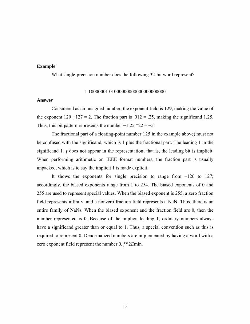
Example
What single-precision number does the following 32-bit word represent?
1 10000001 01000000000000000000000
Answer
Considered as an unsigned number, the exponent field is 129, making the value of
the exponent 129 −127 = 2. The fraction part is .012 = .25, making the significand 1.25.
Thus, this bit pattern represents the number −1.25 *22 = −5.
The fractional part of a floating-point number (.25 in the example above) must not
be confused with the significand, which is 1 plus the fractional part. The leading 1 in the
significand 1 f does not appear in the representation; that is, the leading bit is implicit.
When performing arithmetic on IEEE format numbers, the fraction part is usually
unpacked, which is to say the implicit 1 is made explicit.
It shows the exponents for single precision to range from –126 to 127;
accordingly, the biased exponents range from 1 to 254. The biased exponents of 0 and
255 are used to represent special values. When the biased exponent is 255, a zero fraction
field represents infinity, and a nonzero fraction field represents a NaN. Thus, there is an
entire family of NaNs. When the biased exponent and the fraction field are 0, then the
number represented is 0. Because of the implicit leading 1, ordinary numbers always
have a significand greater than or equal to 1. Thus, a special convention such as this is
required to represent 0. Denormalized numbers are implemented by having a word with a
zero exponent field represent the number 0. f *2Emin.
16
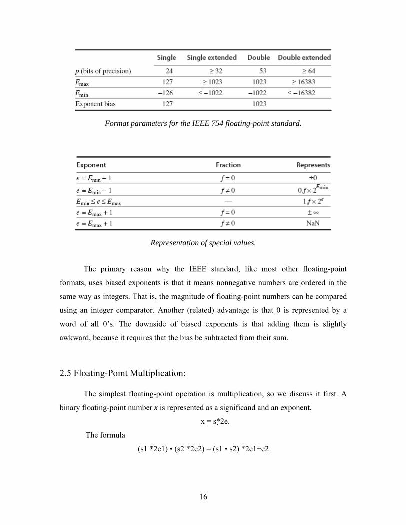
Format parameters for the IEEE 754 floating-point standard.
Representation of special values.
The primary reason why the IEEE standard, like most other floating-point
formats, uses biased exponents is that it means nonnegative numbers are ordered in the
same way as integers. That is, the magnitude of floating-point numbers can be compared
using an integer comparator. Another (related) advantage is that 0 is represented by a
word of all 0’s. The downside of biased exponents is that adding them is slightly
awkward, because it requires that the bias be subtracted from their sum.
2.5 Floating-Point Multiplication:
The simplest floating-point operation is multiplication, so we discuss it first. A
binary floating-point number x is represented as a significand and an exponent,
x = s*2e.
The formula
(s1 *2e1) • (s2 *2e2) = (s1 • s2) *2e1+e2

17
Shows that a floating-point multiply algorithm has several parts. The first part multiplies
the significands using ordinary integer multiplication. Because floating point numbers are
stored in sign magnitude form, the multiplier need only deal with unsigned numbers
(although we have seen that Booth recoding handles signed two’s complement numbers
painlessly). The second part rounds the result. If the significands are unsigned p-bit
numbers (e.g., p = 24 for single precision), then the product can have as many as 2p bits
and must be rounded to a p-bit number. The third part computes the new exponent.
Because exponents are stored with a bias, this involves subtracting the bias from the sum
of the biased exponents.
Example
How does the multiplication of the single-precision numbers
1 10000010 000. . . = –1*23
0 10000011 000. . . = 1*24
Proceed in binary?
Answer
When unpacked, the significands are both 1.0, their product is 1.0, and so the
result is of the form
1 ???????? 000. . .
To compute the exponent, use the formula
Biased exp (e1 + e2) = biased exp(e1) + biased exp(e2) −bias
The bias is 127 = 011111112, so in two’s complement –127 is 100000012. Thus
the biased exponent of the product is
10000010
10000011
+ 10000001
10000110
Since this is 134 decimal, it represents an exponent of 134 −bias = 134 −127 = 7,
as expected.
18
The interesting part of floating-point multiplication is rounding. Since the cases
are similar in all bases, the figure uses human-friendly base 10, rather than base 2.
There is a straightforward method of handling rounding using the multiplier with
an extra sticky bit. If p is the number of bits in the significand, then the A, B, and P
registers should be p bits wide. Multiply the two significands to obtain a 2p-bit product in
the (P,A) registers Using base 10 and p = 3, parts (a) and (b) illustrate that the result of a
multiplication can have either 2p −1 or 2p digits, and hence the position where a 1 is
added when rounding up (just left of the arrow) can vary. Part (c) shows that rounding up
can cause a carry-out.
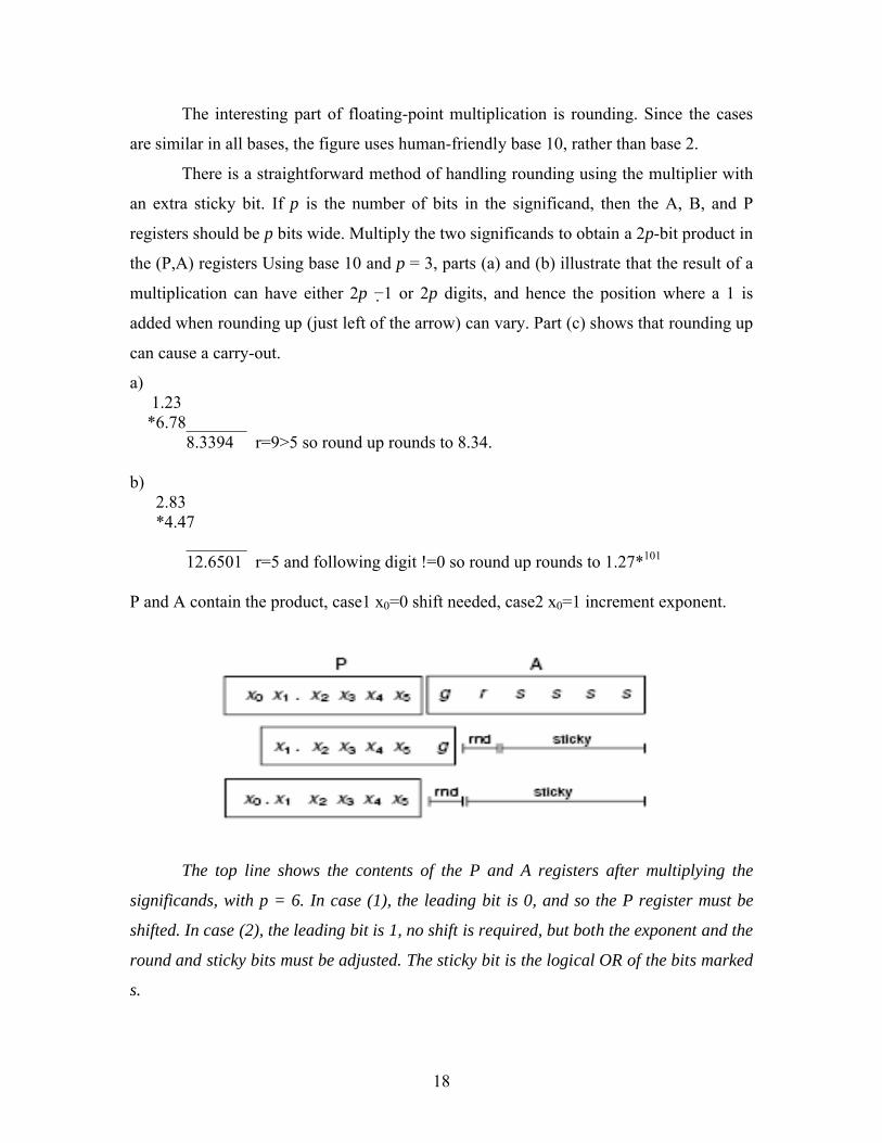
a) 1.23 *6.78_______ 8.3394 r=9>5 so round up rounds to 8.34. b) 2.83 *4.47 _______ 12.6501 r=5 and following digit !=0 so round up rounds to 1.27*101
P and A contain the product, case1 x0=0 shift needed, case2 x0=1 increment exponent.
The top line shows the contents of the P and A registers after multiplying the
significands, with p = 6. In case (1), the leading bit is 0, and so the P register must be
shifted. In case (2), the leading bit is 1, no shift is required, but both the exponent and the
round and sticky bits must be adjusted. The sticky bit is the logical OR of the bits marked
s.
19
During the multiplication, the first p −2 times a bit is shifted into the A register,
OR it into the sticky bit. This will be used in halfway cases. Let s represent the sticky bit,
g (for guard) the most-significant bit of A, and r (for round) the second most-significant
bit of A.
There are two cases:
1) The high-order bit of P is 0. Shift P left 1 bit, shifting in the g bit from A. Shifting
the rest of A is not necessary.
2) The high-order bit of P is 1. Set s= s.v.r and r = g, and add 1 to the exponent.
Now if r = 0, P is the correctly rounded product. If r = 1 and s = 1, then P + 1 is
the product (where by P + 1 we mean adding 1 to the least-significant bit of P). If r = 1
and s = 0, we are in a halfway case, and round up according to the least significant bit of
P. After the multiplication, P = 126 and A = 501, with g = 5, r = 0, s = 1. Since the high-
order digit of P is nonzero, case (2) applies and r := g, so that r = 5, as the arrow indicates
in Figure H.9. Since r = 5, we could be in a halfway case, but s = 1 indicates that the
result is in fact slightly over 1/2, so add 1 to P to obtain the correctly rounded product.
Note that P is nonnegative, that is, it contains the magnitude of the result.
Example
In binary with p = 4, show how the multiplication algorithm computes the product
−5 *10 in each of the four rounding modes.
Answer
In binary, −5 is −1.0102*22 and 10 = 1.0102* 23. Applying the integer
multiplication algorithm to the significands gives 011001002, so P = 01102, A = 01002,
g = 0, r = 1, and s = 0. The high-order bit of P is 0, so case (1) applies. Thus P becomes
11002 and the result is negative.
round to -∞ 11012 add 1 since r.v.s = 1 ⁄ 0 = TRUE
round to +∞ 11002
round to 0 11002
20
round to nearest 11002 no add since r ^ p0 = 1 ^ 0 = FALSE and
r ^ s = 1 ^ 0= FALSE
The exponent is 2 + 3 = 5, so the result is −1.1002 *25 = −48, except when rounding to
−∞, in which case it is −1.1012*25 = −52.
Overflow occurs when the rounded result is too large to be represented. In single
precision, this occurs when the result has an exponent of 128 or higher. If e1 and e2 are
the two biased exponents, then 1 ≤ei ≤254, and the exponent calculation e1 + e2 −127
gives numbers between 1 + 1 −127 and 254 + 254 −127, or between −125 and 381. This
range of numbers can be represented using 9 bits. So one way to detect overflow is to
perform the exponent calculations in a 9-bit adder.
2.6 Denormals: Some Special CasesChecking for underflow is somewhat more complex because of denormals. In
single precision, if the result has an exponent less than −126, that does not necessarily
indicate underflow, because the result might be a denormal number. For example, the
product of (1*2–64) with (1*2–65) is 1 *2–129, and −129 is below the legal exponent limit.
But this result is a valid denormal number, namely, 0.125 *2–126. In general, when the
unbiased exponent of a product dips below −126, the resulting product must be shifted
right and the exponent incremented until the
Rules for implementing the IEEE rounding modes.
exponent reaches −126. If this process causes the entire significand to be shifted out, then
underflow has occurred. The precise definition of underflow is somewhat subtle—see
Section H.7 for details.

21
When one of the operands of a multiplication is denormal, its significand will
have leading zeros, and so the product of the significands will also have leading zeros. If
the exponent of the product is less than –126, then the result is Denormals, so right-shift
and increment the exponent as before. If the exponent is greater than –126, the result may
be a normalized number. In this case, left-shift the product (while decrementing the
exponent) until either it becomes normalized or the exponent drops to –126.
Denormal numbers present a major stumbling block to implementing floating-
point multiplication, because they require performing a variable shift in the multiplier,
which wouldn’t otherwise be needed. Thus, high-performance, floating-point multipliers
often do not handle denormalized numbers, but instead trap, letting software handle them.
A few practical codes frequently underflow, even when working properly, and these
programs will run quite a bit slower on systems that require denormals to be processed by
a trap handler.
Handling of zero operands can be done either testing both operands before
beginning the multiplication or testing the product afterward. Once you detect that the
result is 0, set the biased exponent to 0. The sign of a product is the XOR of the signs of
the operands, even when the result is 0.
2.7 Precision of Multiplication:
In the discussion of integer multiplication, we mentioned that designers must
decide whether to deliver the low-order word of the product or the entire product. A
similar issue arises in floating-point multiplication, where the exact product can be
rounded to the precision of the operands or to the next higher precision. In the case of
integer multiplication, none of the standard high-level languages contains a construct that
would generate a “single times single gets double” instruction. The situation is different
for floating point. Many languages allow assigning the product of two single-precision
variables to a double-precision one and the construction can also be exploited by
numerical algorithms. The best-known case is using iterative refinement to solve linear
systems of equations.

22
3. Standard Algorithms with Architectures
Multiplication is basically a shift add operation. There are, however, many variations on
how to do it. Some are more suitable for FPGA use than others, some of them may be
efficient for a system like CPU. This section explores various verities and attracting
features of multiplication hardware.
3.1 Scaling Accumulator Multipliers:
A Scaling accumulator multiplier performs multiplication using an iterative shift-add
routine. One input is presented in bit parallel form while the other is in bit serial form.
Each bit in the serial input multiplies the parallel input by either 0 or 1. The parallel
input is held constant while each bit of the serial input is presented. Note that the one bit
multiplication either passes the parallel input unchanged or substitutes zero. The result
from each bit is added to an accumulated sum. That sum is shifted one bit before the
result of the next bit multiplication is added to it.
Features:
- Parallel by serial algorithm
- Iterative shift add routine
- N clock cycles to complete
- Very compact design
- Serial input can be MSB or LSB first depending on direction of shift in accumulator
- Parallel output
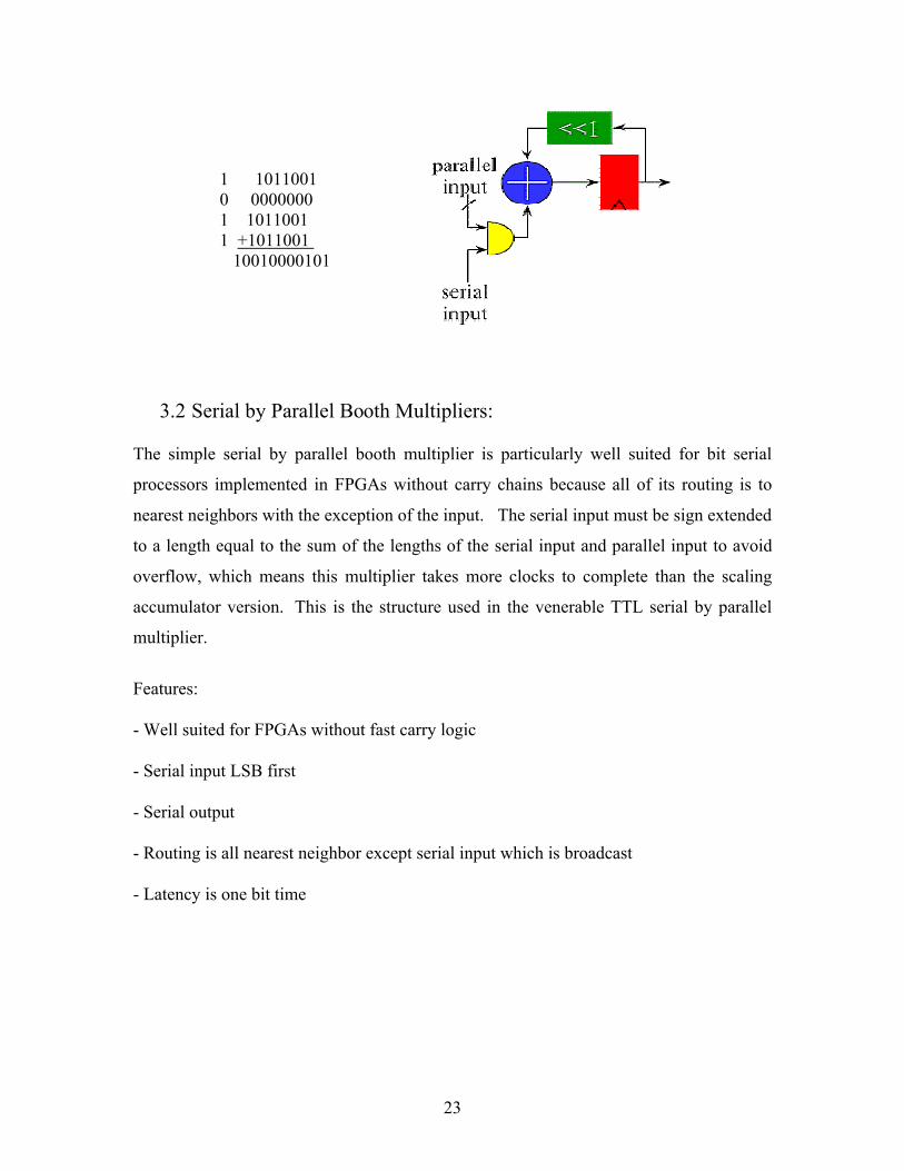
23
1 10110010 0000000 1 10110011 +1011001 10010000101
3.2 Serial by Parallel Booth Multipliers:
The simple serial by parallel booth multiplier is particularly well suited for bit serial
processors implemented in FPGAs without carry chains because all of its routing is to
nearest neighbors with the exception of the input. The serial input must be sign extended
to a length equal to the sum of the lengths of the serial input and parallel input to avoid
overflow, which means this multiplier takes more clocks to complete than the scaling
accumulator version. This is the structure used in the venerable TTL serial by parallel
multiplier.
Features:
- Well suited for FPGAs without fast carry logic
- Serial input LSB first
- Serial output
- Routing is all nearest neighbor except serial input which is broadcast
- Latency is one bit time
24
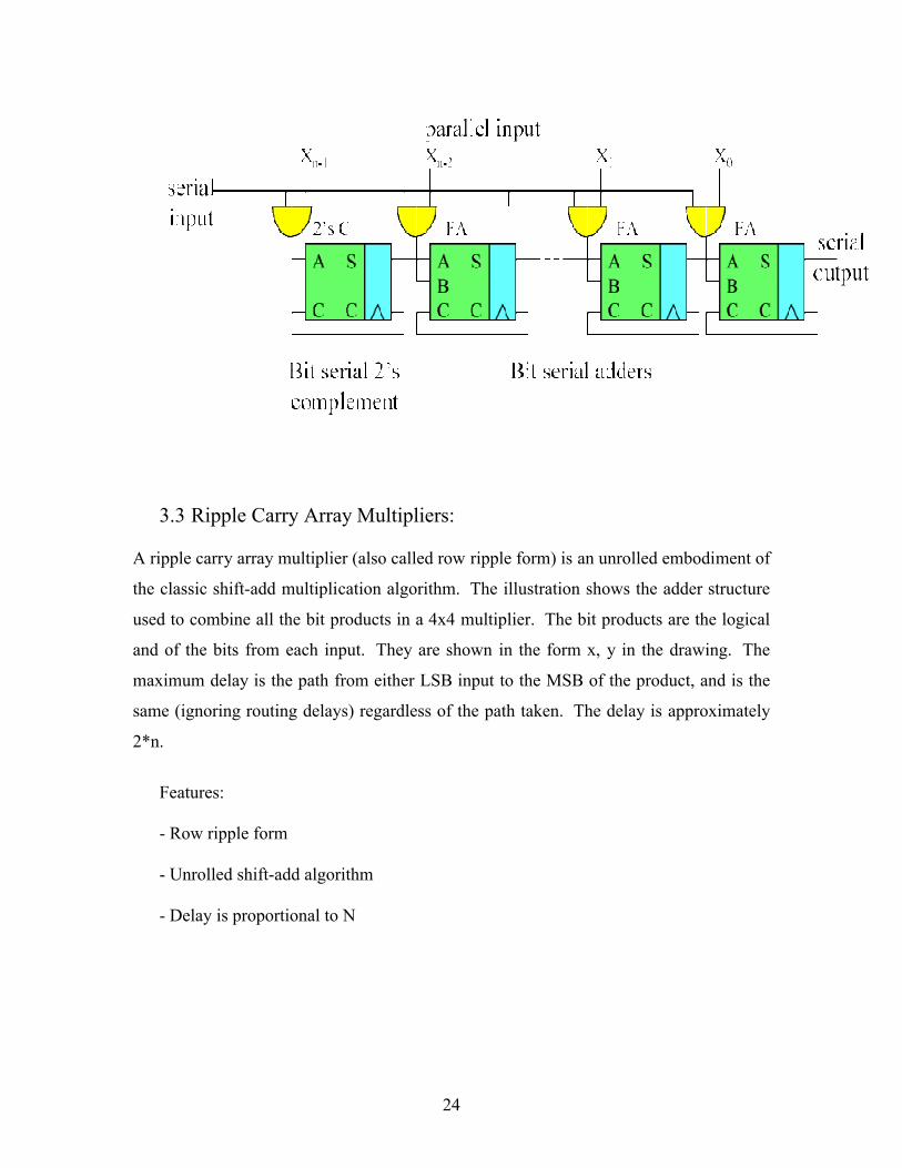
3.3 Ripple Carry Array Multipliers:
A ripple carry array multiplier (also called row ripple form) is an unrolled embodiment of
the classic shift-add multiplication algorithm. The illustration shows the adder structure
used to combine all the bit products in a 4x4 multiplier. The bit products are the logical
and of the bits from each input. They are shown in the form x, y in the drawing. The
maximum delay is the path from either LSB input to the MSB of the product, and is the
same (ignoring routing delays) regardless of the path taken. The delay is approximately
2*n.
Features:
- Row ripple form
- Unrolled shift-add algorithm
- Delay is proportional to N
25
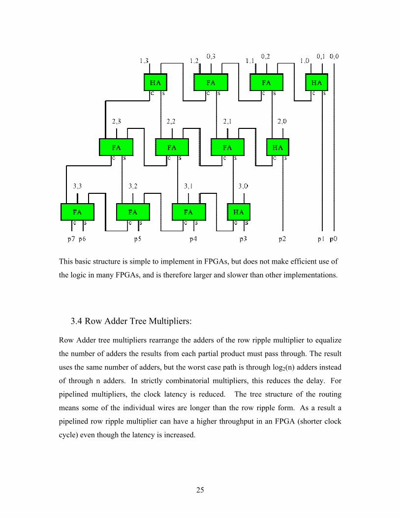
This basic structure is simple to implement in FPGAs, but does not make efficient use of
the logic in many FPGAs, and is therefore larger and slower than other implementations.
3.4 Row Adder Tree Multipliers:
Row Adder tree multipliers rearrange the adders of the row ripple multiplier to equalize
the number of adders the results from each partial product must pass through. The result
uses the same number of adders, but the worst case path is through log2(n) adders instead
of through n adders. In strictly combinatorial multipliers, this reduces the delay. For
pipelined multipliers, the clock latency is reduced. The tree structure of the routing
means some of the individual wires are longer than the row ripple form. As a result a
pipelined row ripple multiplier can have a higher throughput in an FPGA (shorter clock
cycle) even though the latency is increased.
26
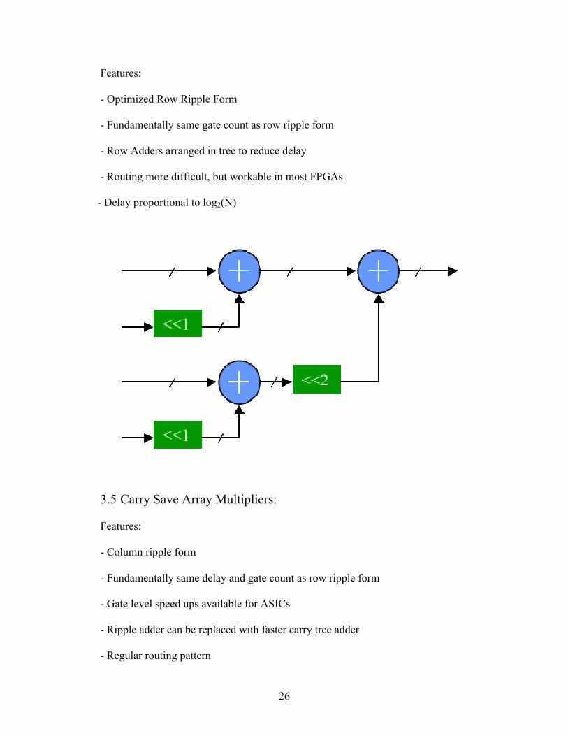
Features:
- Optimized Row Ripple Form
- Fundamentally same gate count as row ripple form
- Row Adders arranged in tree to reduce delay
- Routing more difficult, but workable in most FPGAs
- Delay proportional to log2(N)
3.5 Carry Save Array Multipliers:
Features:
- Column ripple form
- Fundamentally same delay and gate count as row ripple form
- Gate level speed ups available for ASICs
- Ripple adder can be replaced with faster carry tree adder
- Regular routing pattern
27
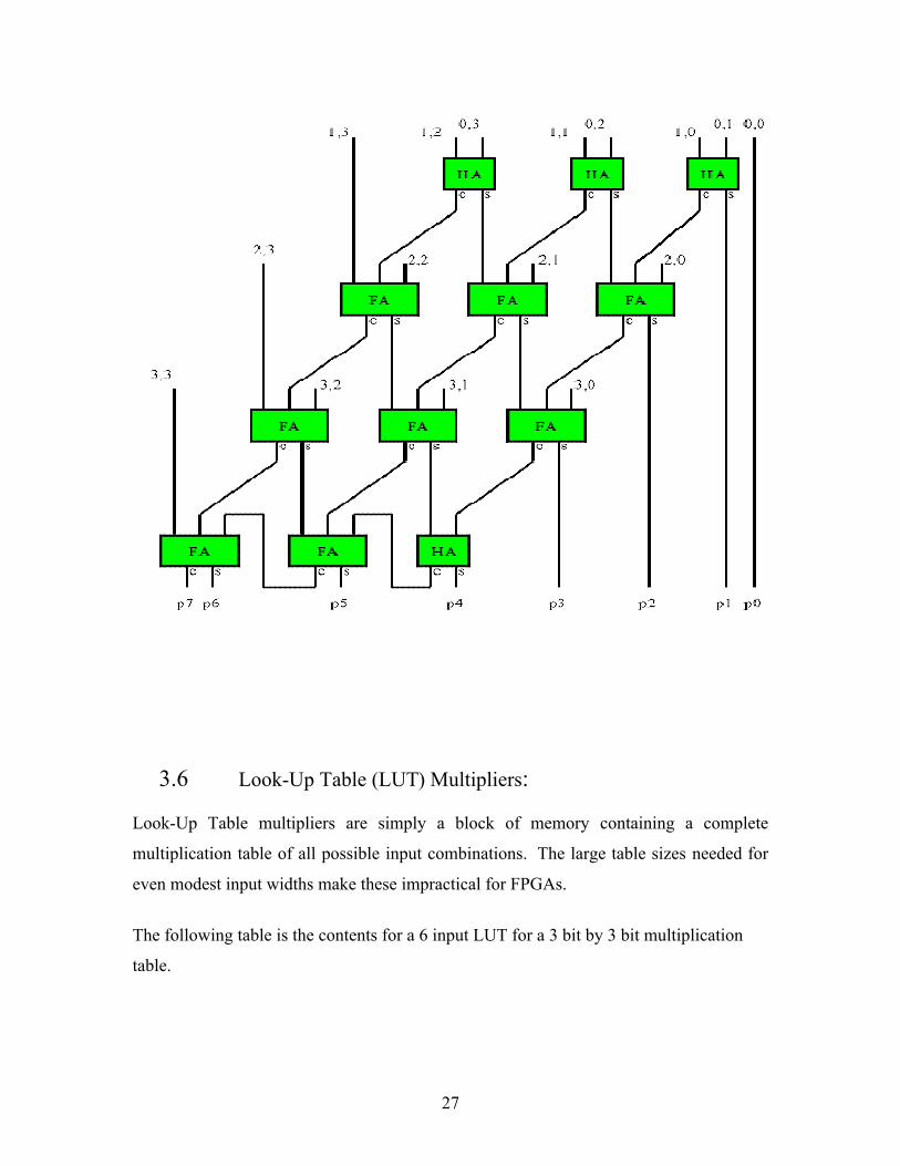
3.6 Look-Up Table (LUT) Multipliers:
Look-Up Table multipliers are simply a block of memory containing a complete
multiplication table of all possible input combinations. The large table sizes needed for
even modest input widths make these impractical for FPGAs.
The following table is the contents for a 6 input LUT for a 3 bit by 3 bit multiplication
table.
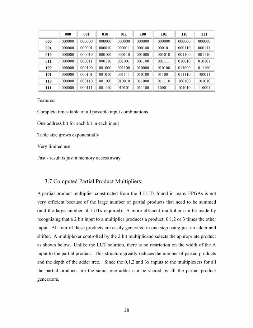
28
000 001 010 011 100 101 110 111
000 000000 000000 000000 000000 000000 000000 000000 000000
001 000000 000001 000010 000011 000100 000101 000110 000111
010 000000 000010 000100 000110 001000 001010 001100 001110
011 000000 000011 000110 001001 001100 001111 010010 010101
100 000000 000100 001000 001100 010000 010100 011000 011100
101 000000 000101 001010 001111 010100 011001 011110 100011
110 000000 000110 001100 010010 011000 011110 100100 101010
111 000000 000111 001110 010101 011100 100011 101010 110001
Features:
Complete times table of all possible input combinations
One address bit for each bit in each input
Table size grows exponentially
Very limited use
Fast - result is just a memory access away
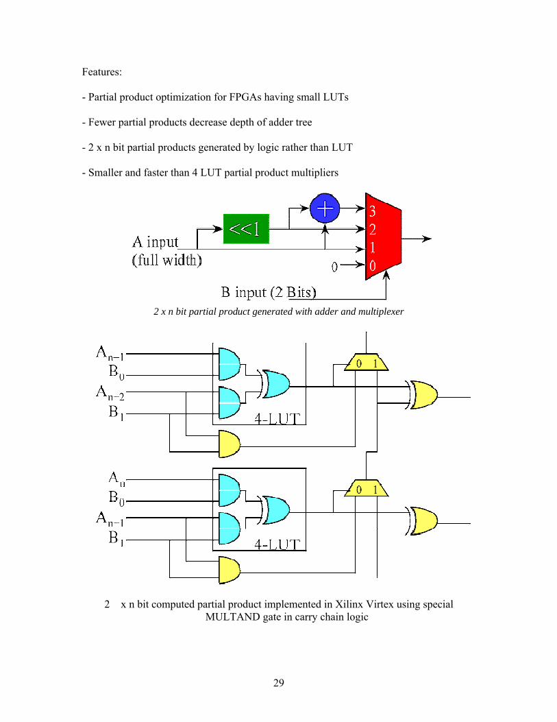
3.7 Computed Partial Product Multipliers:
A partial product multiplier constructed from the 4 LUTs found in many FPGAs is not
very efficient because of the large number of partial products that need to be summed
(and the large number of LUTs required). A more efficient multiplier can be made by
recognizing that a 2 bit input to a multiplier produces a product 0,1,2 or 3 times the other
input. All four of these products are easily generated in one step using just an adder and
shifter. A multiplexer controlled by the 2 bit multiplicand selects the appropriate product
as shown below. Unlike the LUT solution, there is no restriction on the width of the A
input to the partial product. This structure greatly reduces the number of partial products
and the depth of the adder tree. Since the 0,1,2 and 3x inputs to the multiplexers for all
the partial products are the same, one adder can be shared by all the partial product
generators.
29
Features:
- Partial product optimization for FPGAs having small LUTs
- Fewer partial products decrease depth of adder tree
- 2 x n bit partial products generated by logic rather than LUT
- Smaller and faster than 4 LUT partial product multipliers
2 x n bit partial product generated with adder and multiplexer
2 x n bit computed partial product implemented in Xilinx Virtex using special MULTAND gate in carry chain logic
30
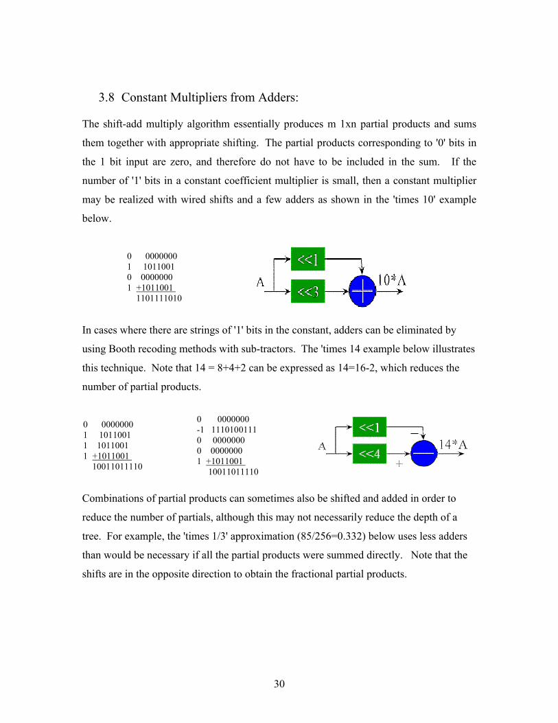
3.8 Constant Multipliers from Adders:
The shift-add multiply algorithm essentially produces m 1xn partial products and sums
them together with appropriate shifting. The partial products corresponding to '0' bits in
the 1 bit input are zero, and therefore do not have to be included in the sum. If the
number of '1' bits in a constant coefficient multiplier is small, then a constant multiplier
may be realized with wired shifts and a few adders as shown in the 'times 10' example
below.
0 00000001 1011001 0 00000001 +1011001 1101111010
In cases where there are strings of '1' bits in the constant, adders can be eliminated by
using Booth recoding methods with sub-tractors. The 'times 14 example below illustrates
this technique. Note that 14 = 8+4+2 can be expressed as 14=16-2, which reduces the
number of partial products.
0 00000001 10110011 10110011 +1011001 10011011110
0 0000000-1 1110100111 0 00000000 00000001 +1011001 10011011110
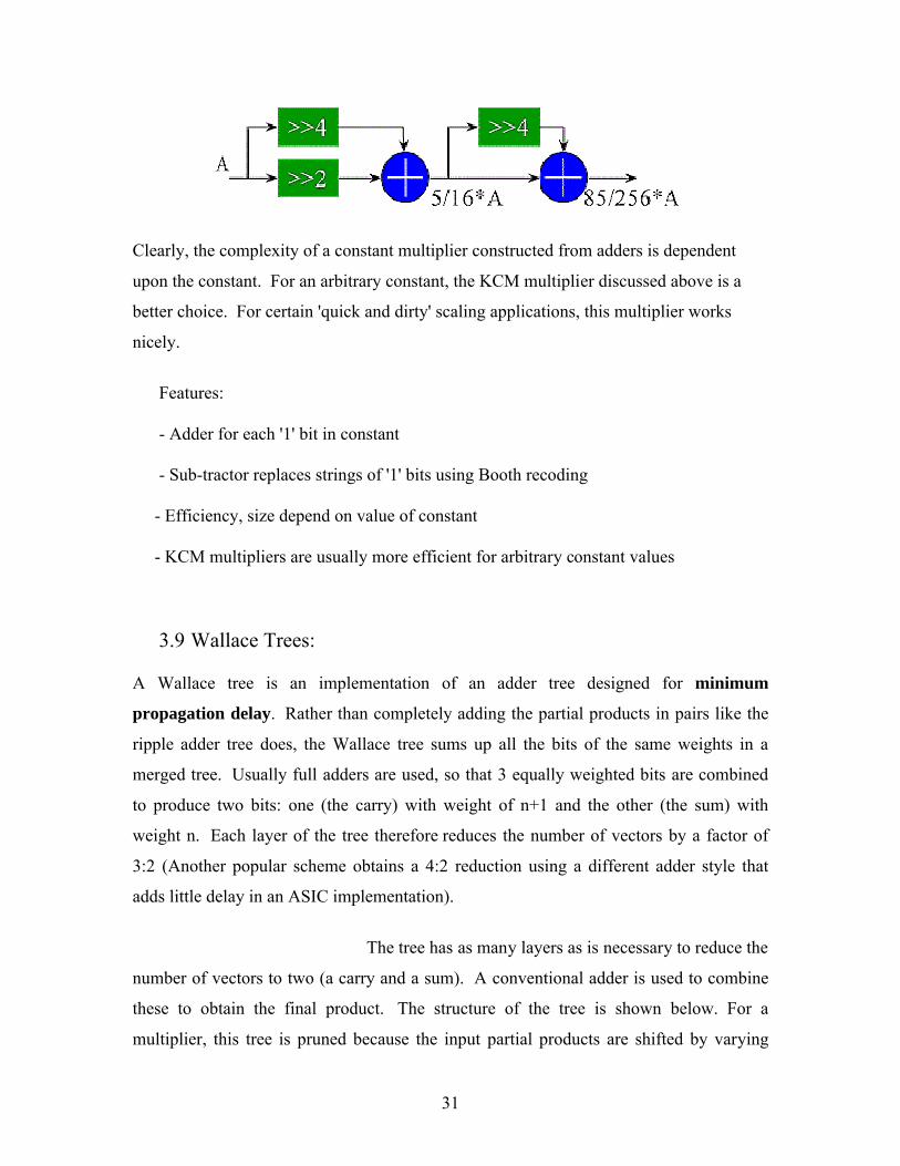
Combinations of partial products can sometimes also be shifted and added in order to
reduce the number of partials, although this may not necessarily reduce the depth of a
tree. For example, the 'times 1/3' approximation (85/256=0.332) below uses less adders
than would be necessary if all the partial products were summed directly. Note that the
shifts are in the opposite direction to obtain the fractional partial products.
31
Clearly, the complexity of a constant multiplier constructed from adders is dependent
upon the constant. For an arbitrary constant, the KCM multiplier discussed above is a
better choice. For certain 'quick and dirty' scaling applications, this multiplier works
nicely.
Features:
- Adder for each '1' bit in constant
- Sub-tractor replaces strings of '1' bits using Booth recoding
- Efficiency, size depend on value of constant
- KCM multipliers are usually more efficient for arbitrary constant values
3.9 Wallace Trees:
A Wallace tree is an implementation of an adder tree designed for minimum
propagation delay. Rather than completely adding the partial products in pairs like the
ripple adder tree does, the Wallace tree sums up all the bits of the same weights in a
merged tree. Usually full adders are used, so that 3 equally weighted bits are combined
to produce two bits: one (the carry) with weight of n+1 and the other (the sum) with
weight n. Each layer of the tree therefore reduces the number of vectors by a factor of
3:2 (Another popular scheme obtains a 4:2 reduction using a different adder style that
adds little delay in an ASIC implementation).
The tree has as many layers as is necessary to reduce the
number of vectors to two (a carry and a sum). A conventional adder is used to combine
these to obtain the final product. The structure of the tree is shown below. For a
multiplier, this tree is pruned because the input partial products are shifted by varying
32
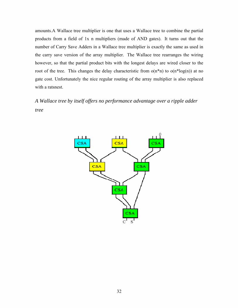
amounts.A Wallace tree multiplier is one that uses a Wallace tree to combine the partial
products from a field of 1x n multipliers (made of AND gates). It turns out that the
number of Carry Save Adders in a Wallace tree multiplier is exactly the same as used in
the carry save version of the array multiplier. The Wallace tree rearranges the wiring
however, so that the partial product bits with the longest delays are wired closer to the
root of the tree. This changes the delay characteristic from o(n*n) to o(n*log(n)) at no
gate cost. Unfortunately the nice regular routing of the array multiplier is also replaced
with a ratsnest.
A Wallace tree by itself offers no performance advantage over a ripple adder
tree

33
A section of an 8 input wallace tree. The wallace tree combines the 8 partial product inputs to two output vectors corresponding to a sum and a carry. A conventional adder is used to combine
these outputs to obtain the complete product..

34
A carry save adder consists of full adders like the more familiar ripple adders, but the
carry output from each bit is brought out to form second result vector rather being than
wired to the next most significant bit. The carry vector is 'saved' to be combined with the
sum later, hence the carry-save moniker.
To the casual observer, it may appear the
propagation delay though a ripple adder tree is the carry propagation multiplied by the
number of levels or o(n*log(n)). In fact, the ripple adder tree delay is really only o(n +
log(n)) because the delays through the adder's carry chains overlap. This becomes
obvious if you consider that the value of a bit can only affect bits of the same or higher
significance further down the tree. The worst case delay is then from the LSB input to
the MSB output (and disregarding routing delays is the same no matter which path is
taken). The depth of the ripple tree is log(n), which is the about same as the depth of the
Wallace tree. This means is that the ripple carry adder tree's delay characteristic is similar
to that of a Wallace tree followed by a ripple adder!
If an adder with a faster carry tree scheme is
used to sum the Wallace tree outputs, the result is faster than a ripple adder tree. The fast
carry tree schemes use more gates than the equivalent ripple carry structure, so the
Wallace tree normally winds up being faster than a ripple adder tree, and less logic than
an adder tree constructed of fast carry tree adders.
A Wallace tree is often slower than a ripple adder tree in an FPGA
Many FPGAs have a highly optimized ripple carry chain connection. Regular logic
connections are several times slower than the optimized carry chain, making it nearly
impossible to improve on the performance of the ripple carry adders for reasonable data
widths (at least 16 bits). Even in FPGAs without optimized carry chains, the delays
caused by the complex routing can overshadow any gains attributed to the Wallace tree
structure. For this reason, Wallace trees do not provide any advantage over ripple adder
trees in many FPGAs. In fact due to the irregular routing, they may actually be slower
and are certainly more difficult to route.
35
Features:
- Optimized column adder tree
- Combines all partial products into 2 vectors (carry and sum)
- Carry and sum outputs combined using a conventional adder
- Delay is log(n)
- Wallace tree multiplier uses Wallace tree to combine 1 x n partial products
- Irregular routing
3.10 Partial Product LUT Multipliers:
Partial Products LUT multipliers use partial product techniques similar to those used in
longhand multiplication (like you learned in 3rd grade) to extend the usefulness of LUT
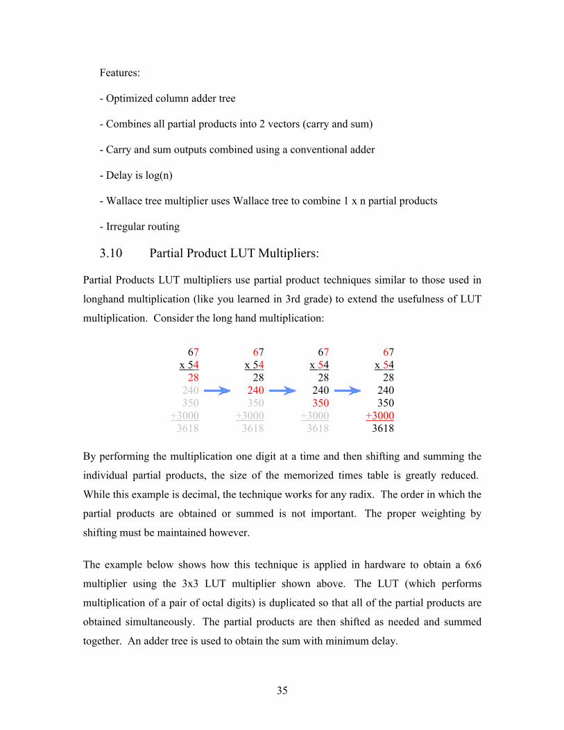
multiplication. Consider the long hand multiplication:
67x 54
28240350
+30003618
67x 54
28 240
350+3000
3618
67x 54
28 240
350+3000
3618
67x 54
28 240
350+3000
3618
By performing the multiplication one digit at a time and then shifting and summing the
individual partial products, the size of the memorized times table is greatly reduced.
While this example is decimal, the technique works for any radix. The order in which the
partial products are obtained or summed is not important. The proper weighting by
shifting must be maintained however.
The example below shows how this technique is applied in hardware to obtain a 6x6
multiplier using the 3x3 LUT multiplier shown above. The LUT (which performs
multiplication of a pair of octal digits) is duplicated so that all of the partial products are
obtained simultaneously. The partial products are then shifted as needed and summed
together. An adder tree is used to obtain the sum with minimum delay.

36
The LUT could be replaced by any other multiplier implementation, since LUT is being
used as a multiplier. This gives the insight into how to combine multipliers of an
arbitrary size to obtain a larger multiplier.
The LUT multipliers shown have matched radices (both inputs are octal). The partial
products can also have mixed radices on the inputs provided care is taken to make sure
the partial products are shifted properly before summing. Where the partial products are
obtained with small LUTs, the most efficient implementation occurs when LUT is square
(ie the input radices are the same). For 8 bit LUTs, such as might be found in an Altera
10K FPGA, this means the LUT radix is hexadecimal.
A more compact but slower version is possible by computing the partial products
sequentially using one LUT and accumulating the results in a scaling accumulator. In this
case, the shifter would need a special control to obtain the proper shift on all the partials.
Features:
- Works like long hand multiplication
- LUT used to obtain products of digits
- Partial products combined with adder tree
37
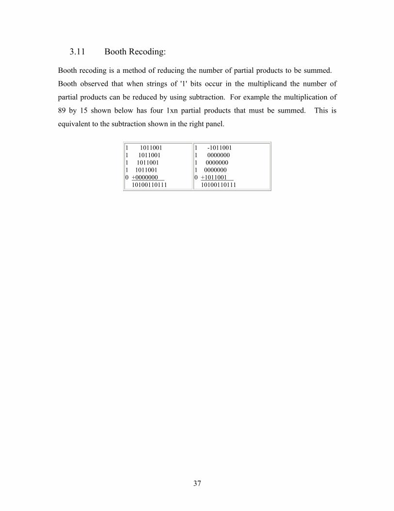
3.11 Booth Recoding:
Booth recoding is a method of reducing the number of partial products to be summed.
Booth observed that when strings of '1' bits occur in the multiplicand the number of
partial products can be reduced by using subtraction. For example the multiplication of
89 by 15 shown below has four 1xn partial products that must be summed. This is
equivalent to the subtraction shown in the right panel.
1 1011001 1 10110011 1011001 1 10110010 +0000000 10100110111
1 -10110011 00000001 0000000 1 00000000 +1011001 10100110111

38
4. Simulation, Synthesis & Analysis.
1. Simulation:
Simulation in system designing refers to check and verification of functionality of
any building block, module, system or subsystem consisting of Basic Blocks. When we
say simulation of any Design essentially it means only logical connections and
verification of Functionality through those logical connections. For simulation Purpose
We used the Model-Sim which is a product of Mentor Graphics.
2. Synthesis:
After Simulation the second important step which tells about the Hardware
realization of any existing or non-existing idea, algorithm in known as Synthesis. For
Synthesis purpose we used the Leonardo Spectrum which is also a product of mentor
Graphics.
Key Fact:
The Key Fact about this whole flow is that “If any problem is there it may have a
realistic solution or may not have, But if it’s having a solution It may give proper results
and may not give (Simulation), If It’s functionality is proper it may be realized or
implemented in Hardware and also may not be (Synthesis).”
At the end of this whole flow we would see that how the basic Algorithms with
slight modifications in either Representations (i.e. Booth Recoding, Pairing of Bits etc.)
or Operations (i.e. Shifting Right in place of Left in Simple Sequential Multiplier.) Have
been implemented and tested in terms of Hardware.
Today the Partition of Hardware and software Modules has reached to a great
extent of conflicts. Now in Designing of any system critically depends on designer as
which parts or function he wants as a Hardware module and for which ones he wants
through Softwares.

39
4.1 Booth Multiplier
4.1.1 VHDL Code:
library ieee;use ieee.std_logic_1164.all, ieee.numeric_std.all;
entity booth is generic(al : natural := 24; bl : natural := 24; ql : natural := 48); port(ain : in std_ulogic_vector(al-1 downto 0); bin : in std_ulogic_vector(bl-1 downto 0); qout : out std_ulogic_vector(ql-1 downto 0); clk : in std_ulogic; load : in std_ulogic; ready : out std_ulogic);end booth;
architecture rtl of booth isbegin process (clk) variable count : integer range 0 to al; variable pa : signed((al+bl) downto 0); variable a_1 : std_ulogic; alias p : signed(bl downto 0) is pa((al + bl) downto al); begin if (rising_edge(clk)) then if load = '1' then p := (others => '0'); pa(al-1 downto 0) := signed(ain); a_1 := '0'; count := al; ready <= '0'; elsif count > 0 then case std_ulogic_vector'(pa(0), a_1) is when "01" => p := p + signed(bin); when "10" => p := p - signed(bin); when others => null; end case;
40
a_1 := pa(0); pa := shift_right(pa, 1); count := count - 1; end if;
if count = 0 then ready <= '1'; end if; qout <= std_ulogic_vector(pa(al+bl-1 downto 0)); end if;end process;end rtl;
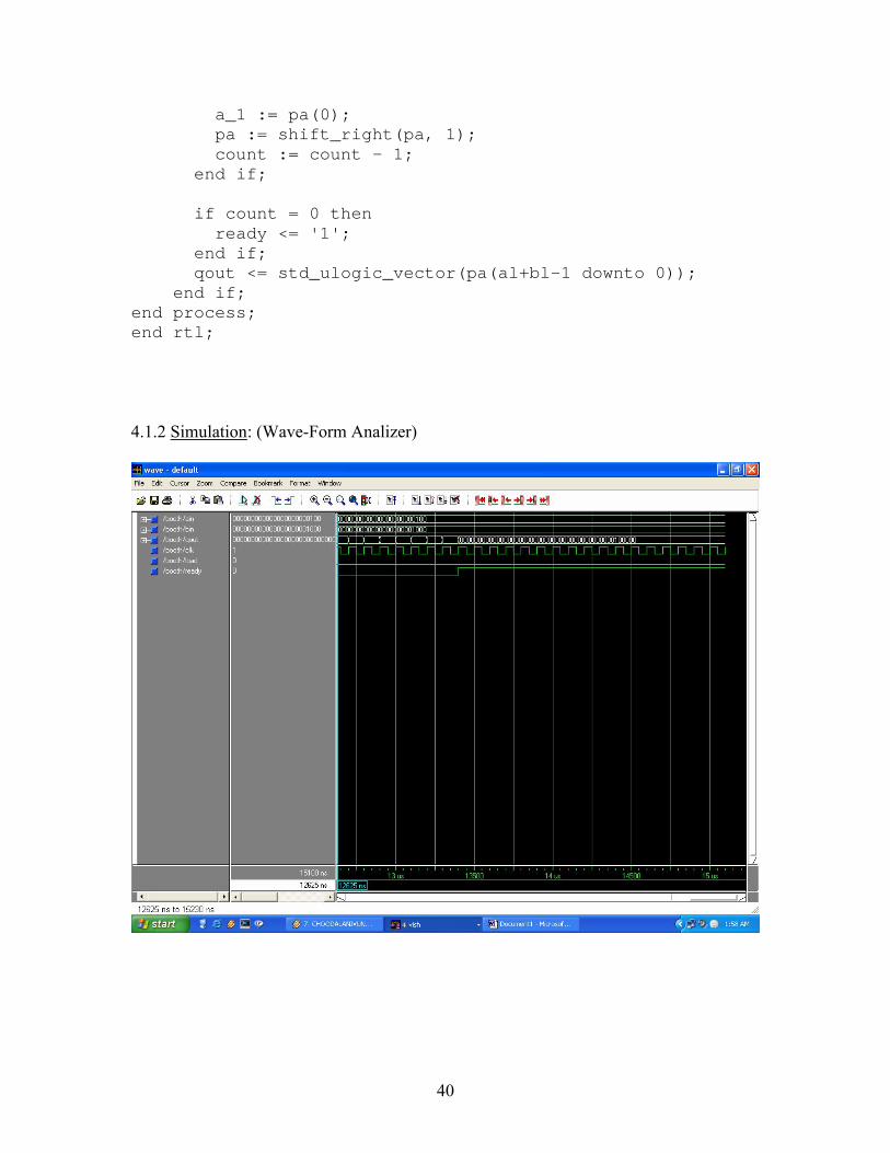
4.1.2 Simulation: (Wave-Form Analizer)
41
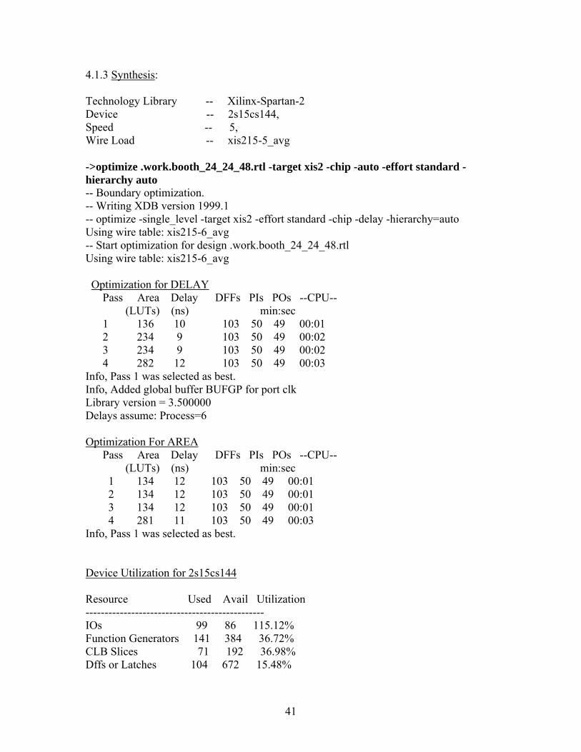
4.1.3 Synthesis:
Technology Library -- Xilinx-Spartan-2Device -- 2s15cs144, Speed -- 5, Wire Load -- xis215-5_avg
->optimize .work.booth_24_24_48.rtl -target xis2 -chip -auto -effort standard -hierarchy auto -- Boundary optimization.-- Writing XDB version 1999.1-- optimize -single_level -target xis2 -effort standard -chip -delay -hierarchy=autoUsing wire table: xis215-6_avg-- Start optimization for design .work.booth_24_24_48.rtlUsing wire table: xis215-6_avg
Optimization for DELAY Pass Area Delay DFFs PIs POs --CPU-- (LUTs) (ns) min:sec 1 136 10 103 50 49 00:01 2 234 9 103 50 49 00:02 3 234 9 103 50 49 00:02 4 282 12 103 50 49 00:03 Info, Pass 1 was selected as best.Info, Added global buffer BUFGP for port clk Library version = 3.500000Delays assume: Process=6
Optimization For AREA Pass Area Delay DFFs PIs POs --CPU-- (LUTs) (ns) min:sec 1 134 12 103 50 49 00:01 2 134 12 103 50 49 00:01 3 134 12 103 50 49 00:01 4 281 11 103 50 49 00:03 Info, Pass 1 was selected as best.
Device Utilization for 2s15cs144
Resource Used Avail Utilization-----------------------------------------------IOs 99 86 115.12%Function Generators 141 384 36.72%CLB Slices 71 192 36.98%Dffs or Latches 104 672 15.48%
42
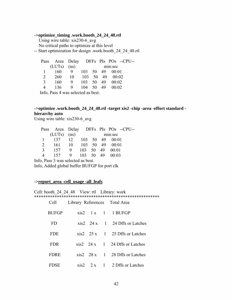
->optimize_timing .work.booth_24_24_48.rtl Using wire table: xis230-6_avg No critical paths to optimize at this level-- Start optimization for design .work.booth_24_24_48.rtl
Pass Area Delay DFFs PIs POs --CPU-- (LUTs) (ns) min:sec 1 160 9 103 50 49 00:01 2 260 10 103 50 49 00:02 3 160 9 103 50 49 00:02 4 136 9 104 50 49 00:02 Info, Pass 4 was selected as best.
->optimize .work.booth_24_24_48.rtl -target xis2 -chip -area -effort standard -hierarchy auto Using wire table: xis230-6_avg
Pass Area Delay DFFs PIs POs --CPU-- (LUTs) (ns) min:sec 1 137 12 103 50 49 00:01 2 161 10 103 50 49 00:01 3 157 9 103 50 49 00:01 4 157 9 103 50 49 00:03 Info, Pass 3 was selected as best.Info, Added global buffer BUFGP for port clk
->report_area -cell_usage -all_leafs
Cell: booth_24_24_48 View: rtl Library: work******************************************************* Cell Library References Total Area
BUFGP xis2 1 x 1 1 BUFGP
FD xis2 24 x 1 24 Dffs or Latches
FDE xis2 25 x 1 25 Dffs or Latches
FDR xis2 24 x 1 24 Dffs or Latches
FDRE xis2 28 x 1 28 Dffs or Latches
FDSE xis2 2 x 1 2 Dffs or Latches
43
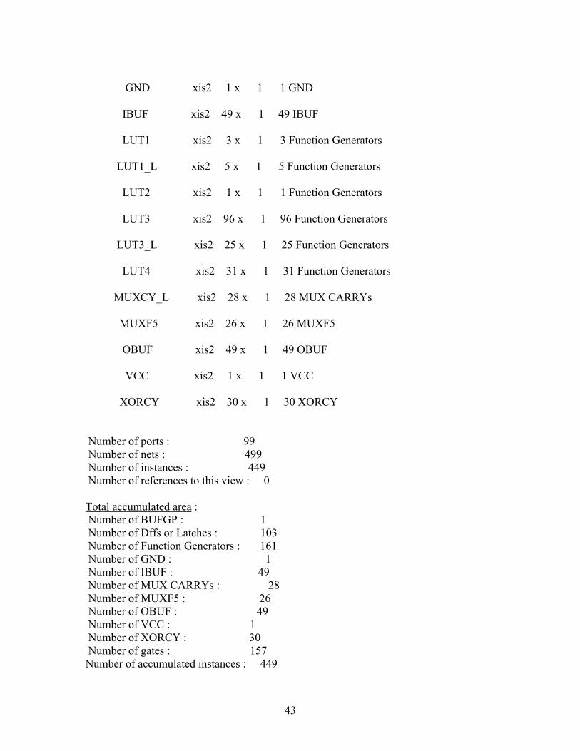
GND xis2 1 x 1 1 GND
IBUF xis2 49 x 1 49 IBUF
LUT1 xis2 3 x 1 3 Function Generators
LUT1_L xis2 5 x 1 5 Function Generators
LUT2 xis2 1 x 1 1 Function Generators
LUT3 xis2 96 x 1 96 Function Generators
LUT3_L xis2 25 x 1 25 Function Generators
LUT4 xis2 31 x 1 31 Function Generators
MUXCY_L xis2 28 x 1 28 MUX CARRYs
MUXF5 xis2 26 x 1 26 MUXF5
OBUF xis2 49 x 1 49 OBUF
VCC xis2 1 x 1 1 VCC
XORCY xis2 30 x 1 30 XORCY
Number of ports : 99 Number of nets : 499 Number of instances : 449 Number of references to this view : 0
Total accumulated area : Number of BUFGP : 1 Number of Dffs or Latches : 103 Number of Function Generators : 161 Number of GND : 1 Number of IBUF : 49 Number of MUX CARRYs : 28 Number of MUXF5 : 26 Number of OBUF : 49 Number of VCC : 1 Number of XORCY : 30 Number of gates : 157Number of accumulated instances : 449

44
Device Utilization for 2s30pq208***********************************************Resource Used Avail Utilization-----------------------------------------------IOs 99 132 75.00%Function Generators 161 864 18.63%CLB Slices 81 432 18.75%Dffs or Latches 103 1296 7.95%-----------------------------------------------
Clock Frequency Report
->report_delay -num_paths 1 -critical_paths -clock_frequency
Clock : Frequencyclk : 101.9 MHz
Critical Path Report
Critical path #1, (path slack = 0.2):
NAME GATE ARRIVAL LOAD-----------------------------------------------------------------------------------clock information not specifieddelay thru clock network 0.00 (ideal)
reg_pa(0)/Q FDE 0.00 2.84 up 3.70ix2006_ix80/LO LUT3_L 0.65 3.49 up 2.10ix2006_ix84/LO MUXCY_L 0.17 3.66 up 2.10ix2006_ix90/LO MUXCY_L 0.05 3.72 up 2.10ix2006_ix96/LO MUXCY_L 0.05 3.77 up 2.10ix2006_ix102/LO MUXCY_L 0.05 3.82 up 2.10ix2006_ix108/LO MUXCY_L 0.05 3.87 up 2.10ix2006_ix114/LO MUXCY_L 0.05 3.93 up 2.10ix2006_ix120/LO MUXCY_L 0.05 3.98 up 2.10ix2006_ix126/LO MUXCY_L 0.05 4.03 up 2.10ix2006_ix132/LO MUXCY_L 0.05 4.08 up 2.10ix2006_ix138/LO MUXCY_L 0.05 4.14 up 2.10ix2006_ix144/LO MUXCY_L 0.05 4.19 up 2.10ix2006_ix150/LO MUXCY_L 0.05 4.24 up 2.10ix2006_ix156/LO MUXCY_L 0.05 4.29 up 2.10ix2006_ix162/LO MUXCY_L 0.05 4.35 up 2.10ix2006_ix168/LO MUXCY_L 0.05 4.40 up 2.10
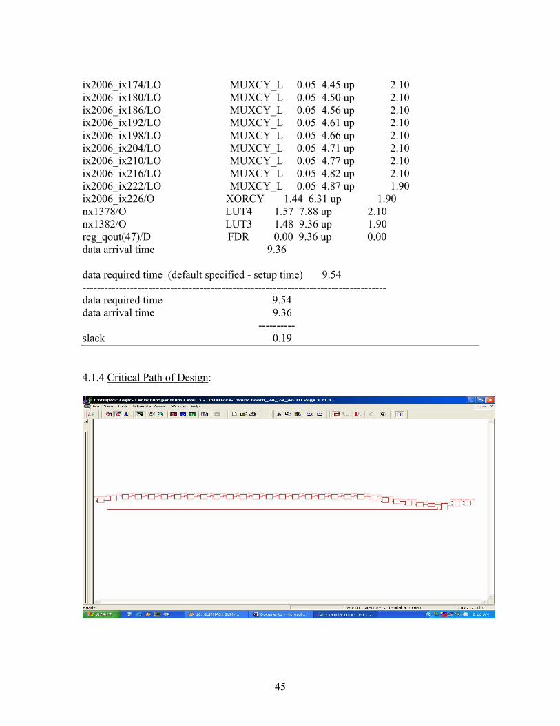
45
ix2006_ix174/LO MUXCY_L 0.05 4.45 up 2.10ix2006_ix180/LO MUXCY_L 0.05 4.50 up 2.10ix2006_ix186/LO MUXCY_L 0.05 4.56 up 2.10ix2006_ix192/LO MUXCY_L 0.05 4.61 up 2.10ix2006_ix198/LO MUXCY_L 0.05 4.66 up 2.10ix2006_ix204/LO MUXCY_L 0.05 4.71 up 2.10ix2006_ix210/LO MUXCY_L 0.05 4.77 up 2.10ix2006_ix216/LO MUXCY_L 0.05 4.82 up 2.10ix2006_ix222/LO MUXCY_L 0.05 4.87 up 1.90ix2006_ix226/O XORCY 1.44 6.31 up 1.90nx1378/O LUT4 1.57 7.88 up 2.10nx1382/O LUT3 1.48 9.36 up 1.90reg_qout(47)/D FDR 0.00 9.36 up 0.00data arrival time 9.36
data required time (default specified - setup time) 9.54-----------------------------------------------------------------------------------data required time 9.54data arrival time 9.36 ----------slack 0.19
4.1.4 Critical Path of Design:

46
4.1.5 Technology Independent Schematic: (Using Primitives of Spartan-II library)

47
4.2 Combinational Multiplier:
To understand the concepts in better way we have carried out the implementation of
small size of combinational Multiplier. The size can be increased by just increasing the
Array size of inputs and outputs.
4.2.1 VHDL Code:
library ieee;use ieee.std_logic_1164.all;use ieee.std_logic_arith.all;use ieee.std_logic_unsigned.all;
-- two 4-bit inputs and one 8-bit outputsentity multiplier is port( num1, num2: in std_logic_vector(1 downto 0);
product: out std_logic_vector(3 downto 0));end multiplier;
architecture behv of multiplier isbeginprocess(num1, num2)
variable num1_reg: std_logic_vector(2 downto 0); variable product_reg: std_logic_vector(5 downto 0);
begin num1_reg := '0' & num1; product_reg := "0000" & num2;
-- algorithm is to repeat shifting/adding for i in 1 to 3 loop if product_reg(0)='1' then
product_reg(5 downto 3) := product_reg(5 downto 3) + num1_reg(2 downto 0);end if;product_reg(5 downto 0) := '0' & product_reg(5 downto
1); end loop;
-- assign the result of computation back to output signal

48
product <= product_reg(3 downto 0); end process; end behv;
4.2.2 Simulation:
4.2.3 Synthesis:
Area optimize effort
optimize .work.multiplier.behv -target xis2 -chip -auto -effort standard -hierarchy auto -- Boundary optimization.-- Writing XDB version 1999.1-- optimize -single_level -target xis2 -effort standard -chip -delay -hierarchy=autoUsing wire table: xis215-6_avg Start optimization for design .work.multiplier.behv

49
Using wire table: xis215-6_avg Pass Area Delay DFFs PIs POs --CPU-- (LUTs) (ns) min:sec 1 4 9 0 4 4 00:00 2 4 9 0 4 4 00:00 3 4 9 0 4 4 00:00 4 4 9 0 4 4 00:00 Info, Pass 1 was selected as best.
Report Area:->report_area -cell_usage -all_leafs
Cell: multiplier View: behv Library: work
******************************************************* Cell Library References Total Area IBUF xis2 4 x 1 4 IBUF LUT2 xis2 1 x 1 1 Function Generators LUT4 xis2 3 x 1 3 Function Generators OBUF xis2 4 x 1 4 OBUF
Number of ports : 8 Number of nets : 16 Number of instances : 12 Number of references to this view : 0
Total accumulated area : Number of Function Generators : 4Number of IBUF : 4 Number of OBUF : 4 Number of gates : 4
Number of accumulated instances : 12
Device Utilization for 2s15cs144***********************************************Resource Used Avail Utilization-----------------------------------------------IOs 8 86 9.30%Function Generators 4 384 1.04%CLB Slices 2 192 1.04%Dffs or Latches 0 672 0.00%
50
Critical Path Report
Critical path #1, (unconstrained path)NAME GATE ARRIVAL LOAD--------------------------------------------------------------------------------num1(0)/ 0.00 0.00 up 1.90num1(0)_ibuf/O IBUF 2.03 2.03 up 2.50product_dup0(3)/O LUT4 1.48 3.51 up 1.90product(3)_obuf/O OBUF 5.10 8.61 up 1.90product(3)/ 0.00 8.61 up 0.00data arrival time 8.61
data required time not specified--------------------------------------------------------------------------------data required time not specifieddata arrival time 8.61 ---------- unconstrained path
4.2.4 Technology Independent Schematic:

51
4.3 Sequential Multiplier:
At the start of multiply: the multiplicand is in "md", the multiplier is in "lo" and "hi"
contains 00000000. This multiplier only works for positive numbers. A booth Multiplier
can be used for twos-complement values.
The VHDL source code for a serial multiplier, using a shortcut model where a signal acts
like a register. "hi" and "lo" are registers clocked by the condition mulclk'event and
mulclk='1'.
At the end of multiply: the upper product is in "hi and the lower product is in "lo."
A partial schematic of just the multiplier data flow is

52
4.3.1 VHDL Code:
library ieee;use ieee.std_logic_1164.all;use ieee.std_logic_unsigned.all;use ieee.std_logic_arith.all;
entity mul_vhdl is port (start,clk,rst : in std_logic; state : out std_logic_vector(1 downto 0)); end mul_vhdl;
architecture asm of mul_vhdl is variable C : integer ; signal M , A : std_logic_vector (8 downto 0); signal Q : std_logic_vector (7 downto 0);type state_type is (j,k,l,n); signal mstate,next_state : state_type;
beginstate_register:process(clk,rst) begin if rst = '1' then mstate <=j; elsif clk'event and clk = '1' then mstate<=next_state; end if; end process;
state_logic : process(mstate,A,Q,M)begin case mstate is when j=> if start='1'then next_state <= k; end if; when k=> A<="000000000"; -- carry<='0'; C := 8; next_state<=l;

53
when l=> C := C - 1; if Q(0)='1' then A = A + M; end if;next_state<=n; when n=> A<= '0' & A( 8 downto 1); Q<= A(0) & Q(7 downto 1); if C = 0 then next_state<=j; else next_state<=k; end if;end case;end process;end asm;
** Verilog Version of same Sequential Multiplier: //accumlator multiplier
module multiplier1(start,clock,clear,binput,qinput,carry, acc,qreg,preg);input start,clock,clear;input [31:0] binput,qinput;output carry;output [31:0] acc,qreg;output [5:0] preg;
//system registersreg carry;reg [31:0] acc,qreg,b;reg [5:0] preg;reg [1:0] prstate,nxstate;parameter t0=2'b00,t1=2'b01, t2=2'b10, t3=2'b11;
wire z;assign z=~|preg;
always @(negedge clock or negedge clear)
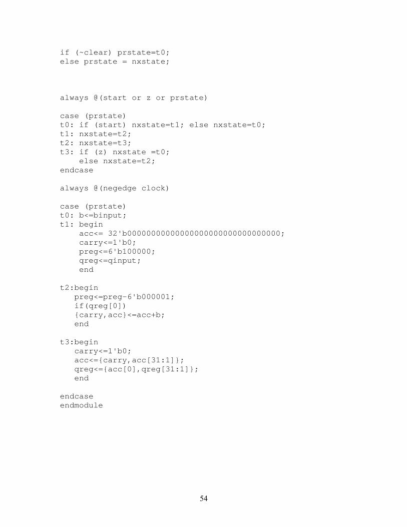
54
if (~clear) prstate=t0;else prstate = nxstate;
always @(start or z or prstate)
case (prstate)t0: if (start) nxstate=t1; else nxstate=t0;t1: nxstate=t2;t2: nxstate=t3;t3: if (z) nxstate =t0; else nxstate=t2;endcase
always @(negedge clock)
case (prstate)t0: b<=binput;t1: begin acc<= 32'b00000000000000000000000000000000; carry<=1'b0; preg<=6'b100000; qreg<=qinput; end
t2:begin preg<=preg-6'b000001; if(qreg[0]) {carry,acc}<=acc+b; end
t3:begin carry<=1'b0; acc<={carry,acc[31:1]}; qreg<={acc[0],qreg[31:1]}; end
endcaseendmodule

55
4.3.2 Simulation:
4.3.3 Synthesis:
->optimize .work.multiplier1.INTERFACE -target xis2 -chip -auto -effort standard -hierarchy auto -- Boundary optimization.-- Writing XDB version 1999.1-- optimize -single_level -target xis2 -effort standard -chip -delay -hierarchy=autoUsing wire table: xis215-6_avg-- Start optimization for design .work.multiplier1.INTERFACE Using wire table: xis215-6_avg Pass Area Delay DFFs PIs POs --CPU-- (LUTs) (ns) min:sec 1 110 9 105 67 71 00:00 2 110 9 105 67 71 00:00 3 110 9 105 67 71 00:08 4 110 9 105 67 71 00:00 Info, Pass 1 was selected as best.

56
Info, Added global buffer BUFGP for port clock -- Writing file .work.multiplier1.INTERFACE_delay.xdb-- Writing XDB version 1999.1
Library version = 3.500000Delays assume: Process=6
Device Utilization for 2s15cs144***********************************************Resource Used Avail Utilization-----------------------------------------------IOs 138 86 160.47%Function Generators 114 384 29.69%CLB Slices 57 192 29.69%Dffs or Latches 106 672 15.77%
***For FREQ f = 50Mhzdata required time (default specified - setup time) 19.54-----------------------------------------------------------------------------------data required time 19.54data arrival time 8.66 ----------slack 10.89-----------------------------------------------------------------------------------
***For FREQ f = 100Mhzdata required time (default specified - setup time) 9.54-----------------------------------------------------------------------------------data required time 9.54data arrival time 8.66 ----------slack 0.89-----------------------------------------------------------------------------------
Device Utilization for 2s50fg256***********************************************Resource Used Avail Utilization-----------------------------------------------IOs 138 176 78.41%Function Generators 114 1536 7.42%CLB Slices 57 768 7.42%Dffs or Latches 106 2082 5.09%
57
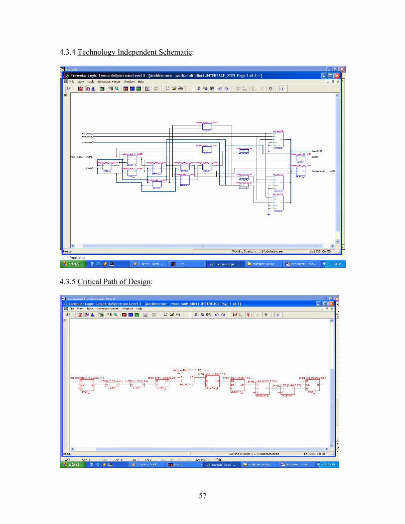
4.3.4 Technology Independent Schematic:
4.3.5 Critical Path of Design:

58
4.4 CSA Wallace-Tree Architecture:
An unsigned multiplier using a carry save adder structure is one of the efficient Design in
implementation of Multipliers. Booth multiplier, two's complement 32-bit multiplicand
by 32-bit multiplier input producing 64-bit product can be implemented using this special
kind of Architecture.
A partial schematic of the multiplier is
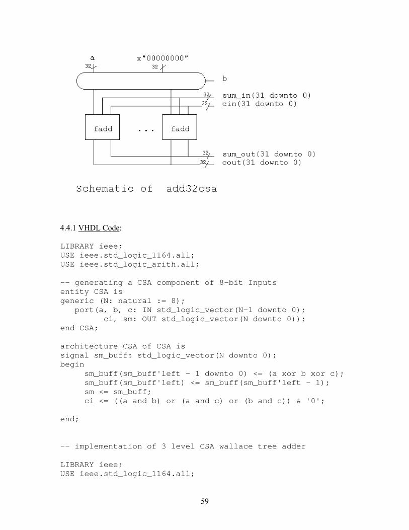
59
4.4.1 VHDL Code:
LIBRARY ieee;USE ieee.std_logic_1164.all;USE ieee.std_logic_arith.all;
-- generating a CSA component of 8-bit Inputs entity CSA isgeneric (N: natural := 8); port(a, b, c: IN std_logic_vector(N-1 downto 0); ci, sm: OUT std_logic_vector(N downto 0));end CSA;
architecture CSA of CSA issignal sm_buff: std_logic_vector(N downto 0);begin
sm_buff(sm_buff'left - 1 downto 0) <= (a xor b xor c); sm_buff(sm_buff'left) <= sm_buff(sm_buff'left - 1);
sm <= sm_buff;ci <= ((a and b) or (a and c) or (b and c)) & '0';
end;
-- implementation of 3 level CSA wallace tree adder
LIBRARY ieee;USE ieee.std_logic_1164.all;

60
USE ieee.std_logic_arith.all;
entity CSA_tree isgeneric(N: natural := 8);port(a0, a1,a2,a3,a4,a5: std_logic_vector (N-1 downto 0); cin, sum: OUT std_logic_vector(N downto 0));end CSA_tree;
architecture wallace_tree of CSA_tree is
component CSA generic(N: natural := 8);port(a, b, c: IN std_logic_vector(N-1 downto 0); ci, sm: OUT std_logic_vector (N downto 0)); end component;
for all: CSA use entity work.CSA(CSA);
signal sl1, cl1, sl2, cl2 : std_logic_vector(8 downto 0);signal sl3, cl3, cl24: std_logic_vector(9 downto 0);signal sl4, cl4, output: std_logic_vector(10 downto 0);signal carry: std_logic_vector(11 downto 0);
begin-- level 1
level1a: CSA port map(a0, a1, a2, cl1, sl1);level1b: CSA port map(a3, a4, a5, cl2, sl2);
-- level 2
level2: CSA generic map (N=>9) port map(sl1, cl1, sl2, cl3, sl3);
-- sign extend by one bit (carry from stage 2 to be fed into stage 3)
cl24 <= cl2(cl2'LEFT) & cl2;
-- level 3
level3: CSA generic map (N=>10) port map(cl24, cl3, sl3, cl4, sl4);

61
-- set carry in to zero
carry(0) <= '0'; gen:for i in 1 to 11 generate
carry(i) <= (sl4(i-1) and cl4(i-1)) or (carry(i-1) and sl4(i-1)) or (carry(i-1) and cl4(i-1));
output(i-1) <= sl4(i-1) xor cl4(i-1) xor carry(i-1);
end generate;end;
4.4.2 Simulation:

62
4.4.3 Synthesis:
->optimize .work.CSA_8.CSA -target xis2 -chip -area -effort standard -hierarchy auto Using wire table: xis215-6_avg-- Start optimization for design .work.CSA_8.CSA Using wire table: xis215-6_avg Pass Area Delay DFFs PIs POs --CPU-- (LUTs) (ns) min:sec 1 16 9 0 24 18 00:00 2 16 9 0 24 18 00:00 3 16 9 0 24 18 00:00 4 16 9 0 24 18 00:00 Info, Pass 1 was selected as best.
->optimize_timing .work.CSA_8.CSA Using wire table: xis215-6_avg-- Start timing optimization for design .work.CSA_8.CSA No critical paths to optimize at this level Info, Command 'optimize_timing' finished successfully->report_area -cell_usage -all_leafs
Cell: CSA_8 View: CSA Library: work******************************************************* Cell Library References Total Area GND xis2 1 x 1 1 GND IBUF xis2 24 x 1 24 IBU LUT3 xis2 16 x 1 16 Function Generators OBUF xis2 18 x 1 18 OBUF
Number of ports : 42 Number of nets : 83 Number of instances : 59 Number of references to this view : 0
Total accumulated area : Number of Function Generators : 16 Number of GND : 1 Number of IBUF : 24 Number of OBUF : 18 Number of gates : 16Number of accumulated instances : 59***********************************************

63
Device Utilization for 2s15cs144***********************************************Resource Used Avail Utilization-----------------------------------------------IOs 42 86 48.84%Function Generators 16 384 4.17%CLB Slices 8 192 4.17%Dffs or Latches 0 672 0.00%-----------------------------------------------
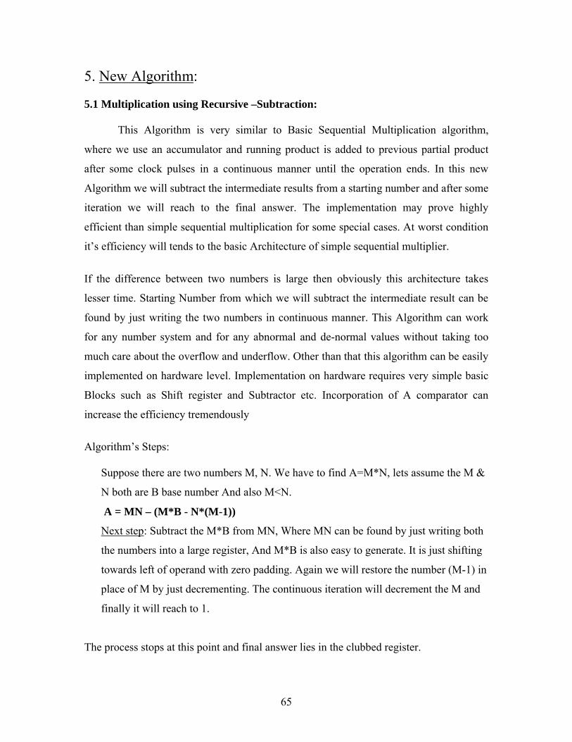
Critical Path ReportFor Frequency = 50 MhzCritical path #1, (path slack = 11.5):
NAME GATE ARRIVAL LOAD------------------------------------------------------------------------------b(7)/ 0.00 0.00 up 1.90b(7)_ibuf/O IBUF 1.85 1.85 up 2.10sm_dup0(8)/O LUT3 1.57 3.42 up 2.10sm(8)_obuf/O OBUF 5.10 8.52 up 1.90sm(8)/ 0.00 8.52 up 0.00data arrival time 8.52
data required time (default specified) 20.00------------------------------------------------------------------------------data required time 20.00data arrival time 8.52 ----slack 11.48
Critical path #2, (path slack = 1.5):
For Frequency = 100 MHz
data required time (default specified) 10.00data required time 10.00data arrival time 8.52--------------------------------------------------------------------slack 1.48
64
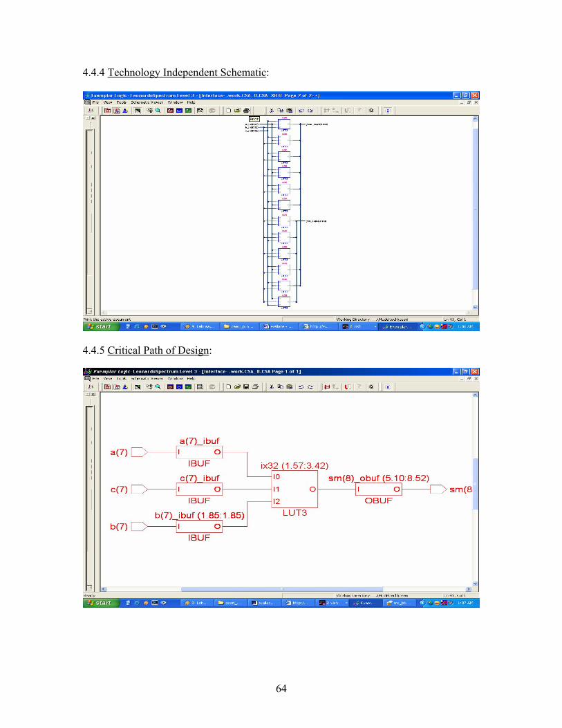
4.4.4 Technology Independent Schematic:
4.4.5 Critical Path of Design:
65
5. New Algorithm:
5.1 Multiplication using Recursive –Subtraction:
This Algorithm is very similar to Basic Sequential Multiplication algorithm,
where we use an accumulator and running product is added to previous partial product
after some clock pulses in a continuous manner until the operation ends. In this new
Algorithm we will subtract the intermediate results from a starting number and after some
iteration we will reach to the final answer. The implementation may prove highly
efficient than simple sequential multiplication for some special cases. At worst condition
it’s efficiency will tends to the basic Architecture of simple sequential multiplier.
If the difference between two numbers is large then obviously this architecture takes
lesser time. Starting Number from which we will subtract the intermediate result can be
found by just writing the two numbers in continuous manner. This Algorithm can work
for any number system and for any abnormal and de-normal values without taking too
much care about the overflow and underflow. Other than that this algorithm can be easily
implemented on hardware level. Implementation on hardware requires very simple basic
Blocks such as Shift register and Subtractor etc. Incorporation of A comparator can
increase the efficiency tremendously
Algorithm’s Steps:
Suppose there are two numbers M, N. We have to find A=M*N, lets assume the M &
N both are B base number And also M<N.
A = MN – (M*B - N*(M-1))
Next step: Subtract the M*B from MN, Where MN can be found by just writing both
the numbers into a large register, And M*B is also easy to generate. It is just shifting
towards left of operand with zero padding. Again we will restore the number (M-1) in
place of M by just decrementing. The continuous iteration will decrement the M and
finally it will reach to 1.
The process stops at this point and final answer lies in the clubbed register.

66
6. Results and Conclusions:
The results obtained from simulation and synthesis of various architectures are compared and tabulated below.
S.No AlgorithmsPerformance/Parameters
Serial Multiplier(Sequential)
Booth Multiplier
CombinationalMultiplier
Wallace Tree Multiplier
1. Optimum Area 110 LUTs 134 LUTs 4 LUTs 16 LUTs
2. Optimum Delay 9 ns 11 ns 9 ns 9 ns
3. Sequential Elements 105 DFFs 103 DFFs ---- ----
4. Input/Output Ports 67 / 71 50 / 49 4 / 4 24 / 18
5. CLB Slices(%) 57(7.42%) 71(36.98%) 2(1.04%) 8(4.17%)
6. Function Generators 114(7.42%) 141(36.72%) 4(1.04%) 16(4.17%)
7. Data Required Time/Arrival Time
9.54 ns8.66 ns
9.54 ns9.36 ns
NA8.61
10 ns8.52 ns
8. Optimum Clock(MHz)
100 101.9 NA 100
9. Slack 0.89 ns 0.19 ns Unconstrained path
1.48 ns
** Serial multiplier is implemented for 32 bit, Booth multiplier 24 bit, combinational for
2 bit and Wallace tree multiplier is 8 bit.
At First Instance It seems that combinational devices may work faster than the Sequential
version of same devices, But this is not true in all the cases. In fact in complex system
designing the sequential version of devises worked faster than the combinational version
because in combinational circuits there is the gate delay involved with each gate which is
putting a constraint on the speed whereas in sequential circuits the clock speed is
constraint which does not get much affected from gate delays. Asynchronous Problem is
also a bigger drawback of the combinational circuits. So now a days the computational
part of systems are combinational and storage elements are sequential which is making a
system robust, cheaper and highly efficient.
67
7. References:
[1]. John L Hennesy & David A. Patterson “Computer Architecture A Quantitative Approach” Second edition; A Harcourt Publishers International Company
[2]. C. S.Wallace, “A suggestion for fast multipliers,” IEEE Trans. Electron. Comput., no. EC-13, pp. 14–17, Feb. 1964.
[3]. M. R. Santoro, G. Bewick, and M. A. Horowitz, “Rounding algorithms for IEEE multipliers,” in Proc. 9th Symp. Computer Arithmetic, 1989, pp. 176–183.
[4]. D. Stevenson, “A proposed standard for binary floating point arithmetic,” IEEE Trans. Comput., vol. C-14, no. 3, pp. 51-62, Mar.
[5]. Naofumi Takagi, Hiroto Yasuura, and Shuzo Yajima. High-speed VLSI multiplication algorithm with a redundant binary addition tree. IEEE Transactions on Computers, C-34(9), Sept 1985.
[6]. “IEEE Standard for Binary Floating-point Arithmetic", ANSUIEEE Std 754-1985, New York, The Institute of Electrical and Electronics Engineers, Inc., August 12, 1985.
[7]. Morris Mano,“Digital Design” Third edition; PHI 2000
[8.] J.F. Wakerly, Digital Design: Principles and Practices, Third Edition, Prentice-Hall,
2000.
[9] J. Bhasker, A VHDL Primer, Third Edition, Pearson, 1999.
[10]. M. Morris Mano,”Computer System Architecture”, Third edition; PHI, 1993.
[11]. John. P. Hayes, “Computer Architecture and Organization”, McGraw Hill, 1998.
[12]. G. Raghurama & T S B Sudarshan, “Introduction to Computer Organization”, EDD Notes for EEE C391, 2003.
Related Documents


![MATLAB practice · 2008. 11. 29. · int32 Signed 32-bit integers in the range [-2147483648,2147483647] (4 bytes per element). single Single-precision floating-point numbers with](https://static.cupdf.com/doc/110x72/61265dff2a37e955a54e9d52/matlab-practice-2008-11-29-int32-signed-32-bit-integers-in-the-range-21474836482147483647.jpg)


