General Description The MAX323/MAX324/MAX325 are precision, dual, SPST analog switches. They are single-supply devices designed to operate from +2.7V to +16V. The MAX323 has two normally open (NO) switches, and the MAX324 has two normally closed (NC) switches. The MAX325 has one NO and one NC switch. Low power consumption (5μW) makes these parts ideal for battery-powered equipment. These switches offer low leakage currents (100pA max) and fast switching speeds (t ON = 150ns max, t OFF = 100ns max). When powered from a 5V supply, the MAX323 series offers 2Ω max matching between channels, 60Ω max on- resistance, and 6Ω max R ON flatness. These switches also offer 5pC max charge injection, and a minimum of 2000V ESD per Method 3015.7. For equivalent devices specified for dual-supply opera- tion, see the MAX320/MAX321/MAX322 data sheet. For quad versions of the MAX320 series, see MAX391/ MAX392/MAX393 data sheet. Applications ● Battery-Operated Systems ● Heads-Up Displays ● Audio and Video Switching ● Test Equipment ● +3V, +5V DACs and ADCs ● Sample-and-Hold Circuits ● Guidance and Control Systems ● Military Radios ● Communications Systems ● PBX, PABX Features ● Low On-Resistance (R ON ), 60Ω max (33Ω typ) ● R ON Matching Between Channels <2Ω ● R ON Flatness <6Ω Max ● Guaranteed Charge Injection <5pC ● Single-Supply Operation (+2.7V to +16V) ● Low Power Consumption, <5μW ● Low Leakage Current Over Temperature, <2.5nA at +85°C ● Fast Switching: t ON <150ns, t OFF <100ns ● Guaranteed Break-Before-Make (MAX325 only) ● TTL/CMOS Logic Compatible 19-0347; Rev 2; 12/20 Ordering Information continued at end of data sheet. * Contact factory for dice specifications. ** Contact factory for availability. PART TEMP. RANGE PIN-PACKAGE MAX323CPA 0°C to +70°C 8 Plastic DIP MAX323CUA 0°C to +70°C 8 µMAX MAX323CSA 0°C to +70°C 8 SO MAX323C/D 0°C to +70°C Dice* MAX323EPA -40°C to +85°C 8 Plastic DIP MAX323ESA -40°C to +85°C 8 SO MAX323EJA -40°C to +85°C 8 CERDIP** MAX323MJA -55°C to +125°C 8 CERDIP** Precision, Single-Supply, SPST Analog Switches MAX323/MAX324/MAX325 Evaluation Kit Available Design Resources Tools and Models Support One Analog Way, Wilmington, MA 01887 U.S.A. | Tel: 781.329.4700 | © 2022 Analog Devices, Inc. All rights reserved. © 2022 Analog Devices, Inc. All rights reserved. Trademarks and registered trademarks are the property of their respective owners. Click here to ask an associate for production status of specific part numbers. Pin Configurations/Functional Diagrams/Truth Tables 8 7 6 5 1 2 3 4 V+ IN1 COM2 NC2 GND IN2 COM1 NC1 8 7 6 5 1 2 3 4 V+ IN1 COM2 NC2 GND IN2 COM1 NO1 SWITCHES SHOWN FOR LOGIC "0" INPUT MAX324 0 1 ON OFF TOP VIEW DIP/SO/μMAX DIP/SO/μMAX DIP/SO/μMAX MAX323 LOGIC SWITCH LOGIC SWITCH LOGIC SWITCH 0 1 OFF ON MAX325 0 1 OFF ON SWITCH 2 ON OFF 8 7 6 5 1 2 3 4 V+ IN1 COM2 NO2 GND IN2 COM1 NO1 MAX323 MAX324 MAX325 Ordering Information

Welcome message from author
This document is posted to help you gain knowledge. Please leave a comment to let me know what you think about it! Share it to your friends and learn new things together.
Transcript
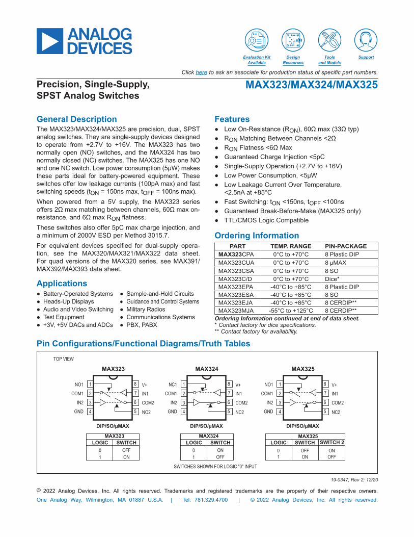
General DescriptionThe MAX323/MAX324/MAX325 are precision, dual, SPST analog switches. They are single-supply devices designed to operate from +2.7V to +16V. The MAX323 has two normally open (NO) switches, and the MAX324 has two normally closed (NC) switches. The MAX325 has one NO and one NC switch. Low power consumption (5μW) makes these parts ideal for battery-powered equipment. These switches offer low leakage currents (100pA max) and fast switching speeds (tON = 150ns max, tOFF = 100ns max).When powered from a 5V supply, the MAX323 series offers 2Ω max matching between channels, 60Ω max on-resistance, and 6Ω max RON flatness.These switches also offer 5pC max charge injection, and a minimum of 2000V ESD per Method 3015.7.For equivalent devices specified for dual-supply opera-tion, see the MAX320/MAX321/MAX322 data sheet. For quad versions of the MAX320 series, see MAX391/MAX392/MAX393 data sheet.
Applications Battery-Operated Systems Heads-Up Displays Audio and Video Switching Test Equipment +3V, +5V DACs and ADCs
Sample-and-Hold Circuits Guidance and Control Systems Military Radios Communications Systems PBX, PABX
Features Low On-Resistance (RON), 60Ω max (33Ω typ) RON Matching Between Channels <2Ω RON Flatness <6Ω Max Guaranteed Charge Injection <5pC Single-Supply Operation (+2.7V to +16V) Low Power Consumption, <5μW Low Leakage Current Over Temperature,
<2.5nA at +85°C Fast Switching: tON <150ns, tOFF <100ns Guaranteed Break-Before-Make (MAX325 only) TTL/CMOS Logic Compatible
19-0347; Rev 2; 12/20
Ordering Information continued at end of data sheet.* Contact factory for dice specifications.** Contact factory for availability.
PART TEMP. RANGE PIN-PACKAGEMAX323CPA 0°C to +70°C 8 Plastic DIPMAX323CUA 0°C to +70°C 8 µMAXMAX323CSA 0°C to +70°C 8 SOMAX323C/D 0°C to +70°C Dice*MAX323EPA -40°C to +85°C 8 Plastic DIPMAX323ESA -40°C to +85°C 8 SOMAX323EJA -40°C to +85°C 8 CERDIP**MAX323MJA -55°C to +125°C 8 CERDIP**
Precision, Single-Supply,SPST Analog Switches
MAX323/MAX324/MAX325
Evaluation Kit Available
Design Resources
Tools and Models
Support
One Analog Way, Wilmington, MA 01887 U.S.A. | Tel: 781.329.4700 | © 2022 Analog Devices, Inc. All rights reserved.
© 2022 Analog Devices, Inc. All rights reserved. Trademarks and registered trademarks are the property of their respective owners.
Click here to ask an associate for production status of specific part numbers.
Pin Configurations/Functional Diagrams/Truth Tables
8
7
6
5
1
2
34
V+IN1
COM2
NC2GND
IN2
COM1
NC1 8
7
6
5
1
2
34
V+IN1
COM2
NC2GND
IN2
COM1
NO1
SWITCHES SHOWN FOR LOGIC "0" INPUT
MAX324
01
ONOFF
TOP VIEW
DIP/SO/µMAX DIP/SO/µMAX DIP/SO/µMAX
MAX323LOGIC SWITCH LOGIC SWITCH LOGIC SWITCH
01
OFFON
MAX325
01
OFFON
SWITCH 2ONOFF
8
7
6
5
1
2
34
V+IN1
COM2
NO2GND
IN2
COM1
NO1
MAX323 MAX324 MAX325
Ordering Information

Voltage Referenced to GND V+ ......................................................................-0.3V to +17V IN_, COM_, NC_, NO_ (Note 1) ..............-0.3V to (V+ + 0.3V)
Continuous Current (any terminal) .....................................30mAPeak Current, COM_, NO_, NC_
(pulsed at 1ms, 10% duty cycle max) ..........................100mAESD per Method 3015.7 ..................................................>2000VContinuous Power Dissipation
Plastic DIP (derate 9.09mW/°C above +70°C) ............727mW Narrow SO (derate 5.88mW/°C above +70°C) ...........471mW
CERDIP (derate 8.00mW/°C above +70°C) ................640mW μMAX (derate 4.10mW/°C above +70°C) ...................330mW
Operating Temperature Ranges MAX32_C_ _ ......................................................0°C to +70°C MAX32_E_ _ .................................................. -40°C to +85°C MAX32_MJA ................................................. -55°C to +125°C
Storage Temperature Range ............................ -65°C to +150°CLead Temperature (soldering, 10sec) .............................+300°C
(V+ = 5V ±10%, GND = 0V, VINH = 2.4V, VINL = 0.8V, TA = TMIN to TMAX, unless otherwise noted.)
Electrical Characteristics—Single +5V Supply
PARAMETER SYMBOL CONDITIONS MIN TYP(Note 2) MAX UNITS
ANALOG SWITCH
Analog Signal RangeVCOM,
VNO, VNC(Note 3) 0 V+ V
On-Resistance RON
V+ = 4.5V, ICOM = 1.0mA,VNO or VNC = 3.5V
TA = +25°C 33 60Ω
TA = TMIN to TMAX 75
On-Resistance Match Between Channels (Note 4) ΔRON
V+ = 5V,ICOM = 1.0mA, VNO or VNC = 3V
TA = +25°C 0.8 2Ω
TA = TMIN to TMAX 4
On-Resistance Flatness (Notes 3, 5)
RFLAT(ON)
V+ = 5V,ICOM = 1.0mA,VNO or VNC = 1V, 2V, 3V
TA = +25°C 2 6Ω
TA = TMIN to TMAX 8
NO or NC Off Leakage Current (Note 6)
INO(OFF)or
INC(OFF)
V+ = 5.5V, VCOM = 1V,VNO or VNC = 4.5V
TA = +25°C -0.1 0.01 0.1nATA = TMIN
to TMAX
C, E -5 5M -40 40
COM Off Leakage Current (Note 6)
ICOM(OFF)
V+ = 5.5V, VCOM = 4.5V, VNO or VNC = 1V
TA = +25°C -0.1 0.1nATA = TMIN
to TMAX
C, E -5 5M -40 40
COM On Leakage Current (Note 6)
ICOM(ON)
V+ = 5.5V, VCOM = 5V, or VNO or VNC = 5V
TA = +25°C -0.2 0.2nATA = TMIN
to TMAX
C, E -10 10M -50 50
www.analog.com Analog Devices 2
MAX323/MAX324/MAX325 Precision, Single-Supply,SPST Analog Switches
Note 1: Signals on NC, NO, COM, or IN exceeding V+ or V- are clamped by internal diodes. Limit forward diode current to maximum current rating.
Absolute Maximum Ratings
Stresses beyond those listed under “Absolute Maximum Ratings” may cause permanent damage to the device. These are stress ratings only, and functional operation of the device at these or any other conditions beyond those indicated in the operational sections of the specifications is not implied. Exposure to absolute maximum rating conditions for extended periods may affect device reliability.
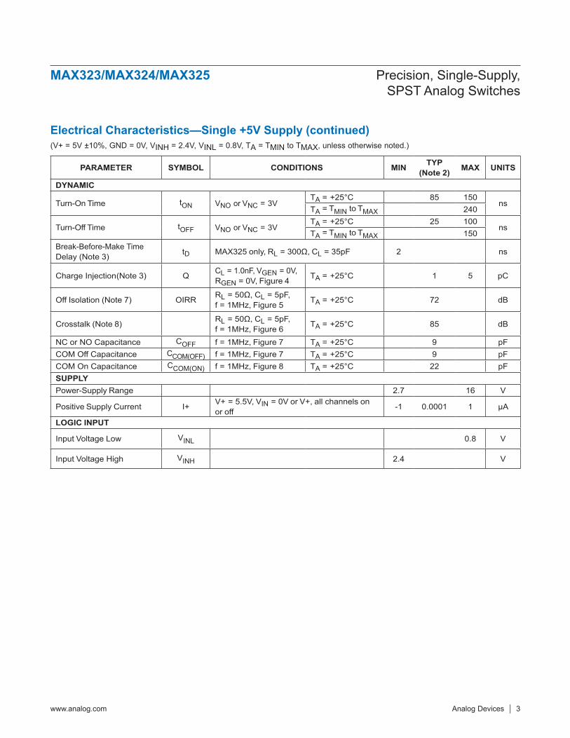
(V+ = 5V ±10%, GND = 0V, VINH = 2.4V, VINL = 0.8V, TA = TMIN to TMAX, unless otherwise noted.)
PARAMETER SYMBOL CONDITIONS MIN TYP(Note 2) MAX UNITS
DYNAMIC
Turn-On Time tON VNO or VNC = 3VTA = +25°C 85 150
nsTA = TMIN to TMAX 240
Turn-Off Time tOFF VNO or VNC = 3VTA = +25°C 25 100
nsTA = TMIN to TMAX 150
Break-Before-Make Time Delay (Note 3) tD MAX325 only, RL = 300Ω, CL = 35pF 2 ns
Charge Injection (Note 3) Q CL = 1.0nF, VGEN = 0V,RGEN = 0V, Figure 4 TA = +25°C 1 5 pC
Off Isolation (Note 7) OIRR RL = 50Ω, CL = 5pF,f = 1MHz, Figure 5 TA = +25°C 72 dB
Crosstalk (Note 8) RL = 50Ω, CL = 5pF,f = 1MHz, Figure 6 TA = +25°C 85 dB
NC or NO Capacitance COFF f = 1MHz, Figure 7 TA = +25°C 9 pFCOM Off Capacitance CCOM(OFF) f = 1MHz, Figure 7 TA = +25°C 9 pFCOM On Capacitance CCOM(ON) f = 1MHz, Figure 8 TA = +25°C 22 pFSUPPLYPower-Supply Range 2.7 16 V
Positive Supply Current I+ V+ = 5.5V, VIN = 0V or V+, all channels on or off -1 0.0001 1 µA
LOGIC INPUT
Input Voltage Low VINL 0.8 V
Input Voltage High VINH 2.4 V
www.analog.com Analog Devices 3
MAX323/MAX324/MAX325 Precision, Single-Supply,SPST Analog Switches
Electrical Characteristics—Single +5V Supply (continued)
(V+ = 3.0V to 3.6V, GND = 0V, VINH = 2.4V, VINL = 0.6V, TA = TMIN to TMAX, unless otherwise noted.)
Note 2: The algebraic convention, where the most negative value is a minimum and the most positive value a maximum, is used in this data sheet.
Note 3: Guaranteed by design.Note 4: ΔRON = ΔRON max - ΔRON min.Note 5: Flatness is defined as the difference between the maximum and minimum value of on-resistance as measured over the
specified analog signal range.Note 6: Leakage parameters are 100% tested at maximum rated hot temperature and guaranteed by correlation at +25°C.Note 7: Off Isolation = 20 log10 [ VCOM ⁄ (VNC or VNO) ], VCOM = output, VNC or VNO = input to off switch.Note 8: Between any two switches.
PARAMETER SYMBOL CONDITIONS MIN TYP(Note 2) MAX UNITS
ANALOG SWITCH
Analog Signal RangeVCOM,
VNO, VNC(Note 3) 0 V+ V
Channel On-Resistance RON
V+ = 3V,ICOM = 1.0mA, VNO or VNC = 1.5V
TA = +25°C 83 175Ω
TA = TMIN to TMAX 275
DYNAMIC
Turn-On Time (Note 3) tON VNO or VNC = 1.5VTA = +25°C 160 400
nsTA = TMIN to TMAX 500
Turn-Off Time (Note 3) tOFF VNO or VNC = 1.5VTA = +25°C 40 125
nsTA = TMIN to TMAX 175
Break-Before-Make Time Delay (Note 3) tD
MAX325 only,RL = 300Ω, CL = 35pF TA = +25°C 2 5 ns
Charge Injection (Note 3) Q CL = 1.0nF, VGEN = 0V, RGEN = 0V TA = +25°C 1 5 pC
SUPPLY
Positive Supply Current I+ V+ = 3.6V, VIN = 0V or V+, all channels on or off -1 1 µA
www.analog.com Analog Devices 4
MAX323/MAX324/MAX325 Precision, Single-Supply,SPST Analog Switches
Electrical Characteristics—Single +3.3V Supply

(TA = +25°C, unless otherwise noted.)
Analog Devices 5www.analog.com
MAX323/MAX324/MAX325 Precision, Single-Supply,SPST Analog Switches
Typical Operating Characteristics
0.0001
ON LEAKAGE CURRENT vs. TEMPERATURE
10
MAX3
23-0
4
TEMPERATURE (°C)
ON LE
AKAG
E (n
A)
0.1
0.001
1
0.01
100
-55 65 85-15 5 25 45-35 105 1250.0001
OFF LEAKAGE CURRENT vs. TEMPERATURE
10
MAX3
23-0
5
TEMPERATURE (°C)
OFF
LEAK
AGE
(nA)
0.1
0.001
1
0.01
100
-55 65 85-15 5 25 45-35 105 125
V+ = 5.5VVCOM = 1VVNC OR VNO = 1V
-30
CHARGE INJECTION vs. VCOM
2
MAX3
23-0
6
VCOM (V)
Q (p
C)
2 5
0
-2
1
-1
3V+ = 5V
1 3 4
00 2 8 10
RON vs. VCOM
60
70 MAX3
23-0
1
VCOM (V)
R ON
(Ω)
4 6 12
40
10
50
20
30
80A: V+ = 3VB: V+ = 5VC: V+ = 12V
A
B
C
00 1 4
RON vs. VCOM OVER TEMPERATURE
50
MAX3
23-0
2
VCOM (V)
R ON
(Ω)
2 3 5
30
10
40
20
60V+ = 5V
A: TA = -55°CB: TA = +25°CC: TA = +85°CD: TA = +125°C
D
C
B
A
00 2
∆RON vs. VCOM OVER TEMPERATURE
MAX3
23-0
3
VCOM (V)
∆RON
(Ω)
3 4
0.6
0.2
0.8
0.4
1
51
A: TA = -55°CB: TA = +25°CC: TA = +85°CD: TA = +125°C
D
BC
A
0
SUPPLY CURRENT vs. TEMPERATURE
78
9 MAX3
23-0
7
TEMPERATURE (°C)
I+ (n
A)
5
12
6
3
4
10
-55 65 85-15 5 25 45-35 105 125
V+ = 5VIN1, IN2 = GND OR V+

Applications InformationLogic LevelsThe MAX323/MAX324/MAX325 are TTL compatible when powered from a single +5V supply. When powered from other supply voltages, TTL compatibility is not guaranteed, and the logic inputs should be driven from rail to rail. For example, with a 15V supply, IN1 and IN2 should be driven low to 0V and high to 15V. Similarly, with a 3.3V supply, IN1 and IN2 should be driven low to 0V and high to 3.3V.Driving IN1 and IN2 rail-to-rail minimizes power consumption.
Analog Signal LevelsAnalog signals that range over the entire supply voltage (V+ to GND) can be switched with very little change in on-resistance over the entire voltage range (see Typical Operating Characteristics). All the switches are bidirec-tional, so NO_, NC_, and COM_ pins can be used as either inputs or outputs.
Power-Supply Sequencing and Overvoltage ProtectionDo not exceed the absolute maximum ratings, because stresses beyond the listed ratings may cause permanent damage to the devices.Proper power-supply sequencing is recommended for all CMOS devices. Always apply V+ before applying analog signals or logic inputs, especially if the analog or logic
signals are not current-limited. If this sequencing is not possible, and if the analog or logic inputs are not current-limited to <30mA, add a small-signal diode (D1) as shown in Figure 1. If the analog signal can dip below GND, add D2. Adding protection diodes reduces the analog signal range to a diode-drop (about 0.7V) below V+ (for D1), and to a diode-drop above ground (for D2). Leakage is unaf-fected by adding the diodes. On-resistance increases by a small amount at low supply voltages. Maximum supply voltage (V+) must not exceed 17V.Adding protection diodes causes the logic thresholds to be shifted relative to the power-supply rails. This can be significant when low supply voltages (5V or less) are used. With a 5V supply, TTL compatibility is not guaran-teed when protection diodes are added. Driving IN1 and IN2 all the way to the supply rails (i.e., to a diodedrop higher than the V+ pin, or to a diode-drop lower than the GND pin) is always acceptable.Protection diodes D1 and D2 also protect against some overvoltage situations. With Figure 1’s circuit, if the sup-ply voltage is below the absolute maximum rating, and if a fault voltage up to the absolute maximum rating is applied to an analog signal pin, no damage will result. For example, with a +5V supply, analog signals up to ±8V will not damage the circuit of Figure 1. If only a single fault signal is present, the fault voltage can rise to +17V or to -12V without damage occurring.
Figure 1. Overvoltage Protection Using Two External Blocking Diodes
PIN NAME FUNCTION
1NO1 Normally Open Analog Switch Terminal
(MAX323/MAX325)
NC1 Normally Closed Analog Switch Terminal (MAX324 only)
2, 6 COM1, COM2 Analog Switch Common Terminal
3, 7 IN2, IN1 Logic Inputs4 GND Ground
5NO2 Normally Open Analog Switch Terminal
(MAX323 only)
NC2 Normally Closed Analog Switch Terminal (MAX324/MAX325)
8 V+ Positive Supply
www.analog.com Analog Devices 6
MAX323/MAX324/MAX325 Precision, Single-Supply,SPST Analog Switches
Pin DescriptionPOSITIVE SUPPLY
COMNO
D2
D1
GND
Vg
V+
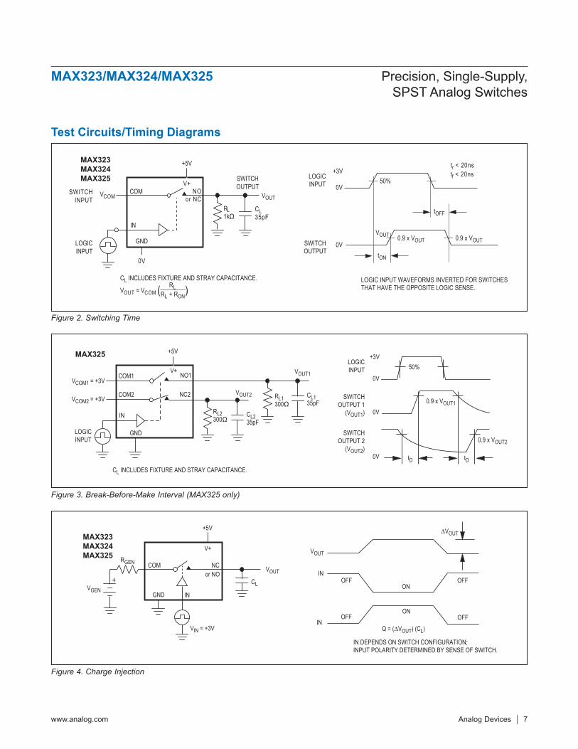
Figure 2. Switching Time
Figure 3. Break-Before-Make Interval (MAX325 only)
Figure 4. Charge Injection
www.analog.com Analog Devices 7
MAX323/MAX324/MAX325 Precision, Single-Supply,SPST Analog Switches
tr < 20nstf < 20ns
50%0V
LOGICINPUT
RL1kΩ
NOor NC
GND
CL INCLUDES FIXTURE AND STRAY CAPACITANCE.
VOUT = VCOM ( RL )RL + RON
SWITCHINPUT
IN
+3V
tOFF
0V
COM
SWITCHOUTPUT
0.9 x VOUT 0.9 x VOUT
tON
VOUTSWITCHOUTPUT
LOGICINPUT
LOGIC INPUT WAVEFORMS INVERTED FOR SWITCHESTHAT HAVE THE OPPOSITE LOGIC SENSE.
V+
CL35pF
+5V
VOUTVCOM
0V
MAX323MAX324MAX325
50%
0.9 x VOUT1
+3V
0V
0V
LOGICINPUT
SWITCHOUTPUT 2
(VOUT2)0V
0.9 x VOUT2
tD tD
LOGICINPUT
RL2300Ω
GND
CL INCLUDES FIXTURE AND STRAY CAPACITANCE.
COM2
IN
COM1
VOUT2
V+
+5V
CL235pF
VCOM1 = +3V
RL1300Ω
VOUT1
CL135pF
NO1
NC2 SWITCHOUTPUT 1
(VOUT1)
VCOM2 = +3V
MAX325
VGENGND
NCor NO
CL
VOUT
V+ VOUT
INOFF
ONOFF
∆VOUT
Q = (∆VOUT) (CL)
COM
IN DEPENDS ON SWITCH CONFIGURATION;INPUT POLARITY DETERMINED BY SENSE OF SWITCH.
OFFON
OFFIN
VIN = +3V
+5V
RGEN
IN
MAX323MAX324MAX325
Test Circuits/Timing Diagrams

Figure 5. Off Isolation
Figure 7. Channel-Off Capacitance
Figure 6. Crosstalk
Figure 8. Channel-On Capacitance
www.analog.com Analog Devices 8
MAX323/MAX324/MAX325 Precision, Single-Supply,SPST Analog Switches
Test Circuits/Timing Diagrams (continued)
IN0V or2.4V
SIGNALGENERATOR 0dBm
+5V10nF
ANALYZERNCor NO
RLGND
COM
COM
V+
MAX323MAX324MAX325
CAPACITANCEMETER NC or
NO
COM
GND
IN 0V or2.4V
10nF +5V
f = 1MHz
V+
MAX323MAX324MAX325
SIGNALGENERATOR 0dBm
+5V10nF
ANALYZER N02
RL
GND
COM1
0V or 2.4VIN1
N01 50Ω
COM2
IN2 0V or2.4V
NC
V+
MAX323MAX324MAX325
CAPACITANCEMETER
NCor NO
COM
GND
IN 0V or2.4V
10nF+5V
f = 1MHz
V+
MAX323MAX324MAX325

* Contact factory for dice specifications.** Contact factory for availability.
PART TEMP. RANGE PIN-PACKAGEMAX324CPA 0°C to +70°C 8 Plastic DIPMAX324CUA 0°C to +70°C 8 µMAXMAX324CSA 0°C to +70°C 8 SOMAX324C/D 0°C to +70°C Dice*MAX324EPA -40°C to +85°C 8 Plastic DIPMAX324ESA -40°C to +85°C 8 SOMAX324EJA -40°C to +85°C 8 CERDIP**MAX324MJA -55°C to +125°C 8 CERDIP**MAX325CPA 0°C to +70°C 8 Plastic DIPMAX325CUA 0°C to +70°C 8 µMAXMAX325CSA 0°C to +70°C 8 SOMAX325C/D 0°C to +70°C Dice*MAX325EPA -40°C to +85°C 8 Plastic DIPMAX325ESA -40°C to +85°C 8 SOMAX325EJA -40°C to +85°C 8 CERDIP**MAX325MJA -55°C to +125°C 8 CERDIP**
www.analog.com Analog Devices 9
MAX323/MAX324/MAX325 Precision, Single-Supply,SPST Analog Switches
Ordering Information (continued) Chip Topography
0.075"(1.90mm)
0.055"(1.40mm)
V+
IN2
V-
IN1
COM2
NO/NC
COM1
NO/NC
TRANSISTOR COUNT: 91SUBSTRATE IS CONNECTED TO V+

www.analog.com Analog Devices 10
MAX323/MAX324/MAX325 Precision, Single-Supply,SPST Analog Switches
L
αC
A1B
DIM
AA1BCDEeHLα
MIN0.0360.0040.0100.0050.1160.116
0.1880.016
0°
MAX0.0440.0080.0140.0070.1200.120
0.1980.026
6°
MIN0.910.100.250.132.952.95
4.780.410°
MAX1.110.200.360.183.053.05
5.030.666°
INCHES MILLIMETERS
8-PIN µMAXMICROMAX SMALL OUTLINE
PACKAGE
0.650.0256
A
e
E H
D
0.101mm0.004 in
DIM
AA1A2A3B
B1C
D1E
E1e
eAeBL
MIN–
0.0150.1250.0550.0160.0450.0080.0050.3000.2400.1000.300
–0.115
MAX0.200
–0.1750.0800.0220.0650.0120.0800.3250.310
––
0.4000.150
MIN–
0.383.181.400.411.140.200.137.626.102.547.62
–2.92
MAX5.08
–4.452.030.561.650.302.038.267.87
––
10.163.81
INCHES MILLIMETERS
Plastic DIPPLASTIC
DUAL-IN-LINEPACKAGE(0.300 in.)
DIM
DDDDDD
MIN0.3480.7350.7450.8851.0151.14
MAX0.3900.7650.7650.9151.0451.265
MIN8.84
18.6718.9222.4825.7828.96
MAX9.91
19.4319.4323.2426.5432.13
INCHES MILLIMETERSPINS
81416182024
C
A A2
E1D
E
eAeB
A3
B1B
0° - 15°A1L
D1
e
Package InformationFor the latest package outline information and land patterns (footprints), go to www.maximintegrated.com/packages. Note that a “+”, “#”, or “-” in the package code indicates RoHS status only. Package drawings may show a different suffix character, but the drawing pertains to the package regardless of RoHS status.

www.analog.com Analog Devices 11
MAX323/MAX324/MAX325 Precision, Single-Supply,SPST Analog Switches
Package Information (continued)For the latest package outline information and land patterns (footprints), go to www.maximintegrated.com/packages. Note that a “+”, “#”, or “-” in the package code indicates RoHS status only. Package drawings may show a different suffix character, but the drawing pertains to the package regardless of RoHS status.
DIM
AA1BCEeHL
MIN0.0530.0040.0140.0070.150
0.2280.016
MAX0.0690.0100.0190.0100.157
0.2440.050
MIN1.350.100.350.193.80
5.800.40
MAX1.750.250.490.254.00
6.201.27
INCHES MILLIMETERS
21-0041A
SOSMALL OUTLINE
PACKAGE(0.150 in.)
DIM
DDD
MIN0.1890.3370.386
MAX0.1970.3440.394
MIN4.808.559.80
MAX5.008.75
10.00
INCHES MILLIMETERSPINS
81416
1.270.050
L
0°-8°
HE
D
e
A
A1 C
0.101mm0.004in.
B

www.analog.com Analog Devices 12
MAX323/MAX324/MAX325 Precision, Single-Supply,SPST Analog Switches
Package Information (continued)For the latest package outline information and land patterns (footprints), go to www.maximintegrated.com/packages. Note that a “+”, “#”, or “-” in the package code indicates RoHS status only. Package drawings may show a different suffix character, but the drawing pertains to the package regardless of RoHS status.
DIM
AB
B2CE
eAeLQS1
MIN–
0.0140.0380.0080.2200.290
0.1250.0150.005
MAX0.2250.0230.0650.0150.3100.320
0.2000.070
–
MIN–
0.360.970.205.597.37
3.180.380.13
MAX5.720.581.650.387.878.13
5.081.78
–
INCHES MILLIMETERS
Ceramic SBCERAMIC SIDEBRAZE
PACKAGE(0.300 in.)
DIM
DDDDDD
MIN––––––
MAX0.5500.7850.8400.9601.0601.280
MIN––––––
MAX13.9719.9421.3424.3826.9232.51
INCHES MILLIMETERSPINS
81416182024
2.54
CL
0°-15°
D E
eA
A
B2B
e
Q
S1
0.100

REVISION NUMBER
REVISION DATE DESCRIPTION PAGES
CHANGED
2 12/20 Updated Pin Configurations in Pin Configurations/Functional Diagrams/Truth Tables, added Revision History. 1, 13
MAX323/MAX324/MAX325 Precision, Single-Supply,SPST Analog Switches
Revision History
w w w . a n a l o g . c o m Analog Devices 13
Information furnished by Analog Devices is believed to be accurate and reliable. However, no responsibility is assumed by Analog Devices for its use, nor for any infringements of patents or other rights of third parties that may result from its use.Specifications subject to change without notice. No license is granted by implication or otherwise under any patent or patent rights of Analog Devices. Trademarks and registered trademarks are the property of their respective owners.
Related Documents