EFFECTS OF GEOMETRICAL ORDER ON THE LINEAR AND NONLINEAR OPTICAL PROPERTIES OF METAL NANOPARTICLES By Matthew David McMahon Dissertation Submitted to the Faculty of the Graduate School of Vanderbilt University in partial fulfillment of the requirements for the degree of DOCTOR OF PHILOSOPHY in Physics December, 2006 Nashville, Tennessee Approved: Professor Richard F. Haglund, Jr. Professor Charles A. Brau Professor David E. Cliffel Professor Sokrates T. Pantelides Professor Robert A. Weller

Welcome message from author
This document is posted to help you gain knowledge. Please leave a comment to let me know what you think about it! Share it to your friends and learn new things together.
Transcript
EFFECTS OF GEOMETRICAL ORDER ON THE LINEAR AND NONLINEAR
OPTICAL PROPERTIES OF METAL NANOPARTICLES
By
Matthew David McMahon
Dissertation
Submitted to the Faculty of the
Graduate School of Vanderbilt University
in partial fulfillment of the requirements
for the degree of
DOCTOR OF PHILOSOPHY
in
Physics
December, 2006
Nashville, Tennessee
Approved:
Professor Richard F. Haglund, Jr.
Professor Charles A. Brau
Professor David E. Cliffel
Professor Sokrates T. Pantelides
Professor Robert A. Weller

Copyright © 2006 by Matthew David McMahon
All Rights Reserved

In memory of my grandfathers, Raymond E. McMahon and James A. O’Neill
To my beloved wife, Carissa
For my children, Bethany and Andrew
iii
FOREWORD
Why on earth, you ask, would anyone spend five years of his life – in his twenties no
less! – studying the optical properties of metal nanoparticles? The answer is largely pro-
vided by what I now call Weller’s First Criterion:
Am I interested?
In short: Yes! For as long as I can remember, I have been fascinated with light and
color. Earth’s ubiquitous sun was for centuries the best light source available to scientists
– even sophisticated twentieth-century techniques like Raman scattering were first dis-
covered with sunlight – and so it served me in the laboratory of youth. I recall the im-
mense power of sunlight being demonstrated on a crisp New England autumn morning by
a cousin with a magnifying glass and a fleeting pyromaniac streak. The late-afternoon
rainbows of August are still some of the best examples of profound beauty in nature. It is
this combination of power and beauty that attracts me to the study of light.
Over the years, I have also developed a fascination with certain theological parallels
which may be drawn. The Christian Bible claims that “God is Light”*; and, regardless of
how literally this statement was meant to be taken, it is indubitable that the lightlike un-
ion of power and beauty was recognized some thousands of years ago as a reflection of
the divine nature. Undoubtedly, better physicists and better theologians have conceived
deeper parallels; I myself only claim to have been struck by the tirelessness, timelessness
and constancy of light, and the infinite breadth of the electromagnetic spectrum. I have
tried not to think too hard about the theological hubris therefore implicit in the idea of
controlling light on the finest scales, which is more or less the subject of my research; * I John 1:5.
iv

and yet I feel the force of the ancient command to “subdue [the earth]”†. Or to para-
phrase King Solomon, “It is the glory of God to conceal a thing; but the honour of physi-
cists is to search out a matter.” ‡
The idea of controlling the arrangement of little bits of precious metal on spatial
scales literally un-resolvable by human eyes is similarly compelling for me. It seems
wondrous that in spite of their diminutive dimensions, they display brilliant colors that
are macroscopically visible – creating breathtaking connections between the realms of the
seen and the unseen. Perhaps it is appropriate, then, that the best-known historical use of
metal nanoparticles is in the coloration of medieval stained glass windows.
Matthew McMahon
Nashville, Tennessee
† Genesis 1:28. ‡ Proverbs 25:2 (KJV).
v
ACKNOWLEDGMENTS
It has been said that when God gives gifts, they nearly always come in the form of a
person. This has proven true during my graduate career, and my profuse thanks are due
both to God and to the people who made these last five years a rewarding and enjoyable –
it might be more accurate to say relentlessly enjoyable – interval.
This dissertation would never have come to pass without the consistent vision, steady
example and patient encouragement of my adviser, Prof. Richard Haglund. It has been a
delight to work under his supervision. When I first came to Vanderbilt I worked exten-
sively with Prof. Robert Weller, and I greatly appreciate his teaching and direction in
those early years as well as his service on my committee. I also thank my committee
members Prof. Charles Brau, Prof. David Cliffel and Prof. Sokrates Pantelides for their
teaching, suggestions and criticism.
Prof. Royal Albridge was largely responsible for my coming to Vanderbilt through
his leadership of the NSF Research Experience for Undergraduates program. Prof. Len
Feldman (a Drew alumnus) was instrumental in bringing me to Nashville as well, and I
enjoyed working closely with him during my first three years of graduate school. The
students in the program, especially Kat Camenisch, April Teske, Cyndi Heiner, Eric
Chancellor and Hugo Valle, made the summer of 2000 a memorable one.
I am proud to count many current and former physics students and faculty among my
friends. I would like to thank a few of them specifically: Dr. Dennis Fong, Prof. Rene
Lopez, Dr. Michael Papantonakis, Dr. Ricardo Ruiz, Prof. Ken Schriver, Stephen John-
son, Jae Suh, Eugene Donev, Davon Ferrara, Nicole Dygert, Chris and Katie Goodin, Ja-
vi
son Rohner, Ron Belmont, Ben and Heather McDonald, Chris Bowie, Andrej Halabica,
Chase Boulware and Jonathan Jarvis. I also thank Tim Miller for patiently teaching me
SEM while he was completing his own graduate work, and Michelle Baltz-Knorr for an
exhortation about priorities which I have never forgotten.
The office staff in the Physics and Engineering departments were consistently help-
ful; thanks to Jane Fall, Janell Lees, Carol Soren, and Valerie Mauro.
The work described in this dissertation was every bit a collaborative venture. For
their specific contributions to the work contained herein, I thank Prof. Richard F.
Haglund, Jr., Prof. Rene Lopez, Prof. Robert Weller, Prof. Len Feldman, and Davon
Ferrara.
The physics faculty of Drew University, my alma mater, prepared me well for my
studies at Vanderbilt. I thank in particular Prof. Jim Supplee, still the most entertaining
(and caffeinated!) lecturer I have encountered; my academic adviser, Prof. Robert Fen-
stermacher, whose laboratory instruction confirmed my fascination with experimental
physics; and Prof. Ashley Carter, whose encouragement to continue my studies was a re-
serve which I drew upon regularly at Vanderbilt.
Spiritual support was a critical part of my life at Vanderbilt, preventing burnout; al-
lowing time for prayer, meditation, and worship; and providing essential outlets for life
beyond physics. The Vanderbilt Graduate Christian Fellowship was a constant source of
spiritual, mental and philosophical stimulation, and was a springboard for many close
friendships; I cannot overestimate its impact on my personal growth in the last five years.
An abbreviated list of people includes Dr. Jon Stadler, Dr. Mark Bray, Dr. Franklin Mul-
lins, Roger Jackson, Natasha Smith, Kara Kilpatrick, Dr. Aaron and Vanessa Simmons,
vii

Dr. Barry and Linnea Robinson, Ed Briscoe, John and Damariz Lamb, Dr. David and Jen
Dismuke, Chris and Trish Pino, Les and Jocelyn Carter, Brian Lennon, Dr. Monica Smat-
lak, Lauri Hornbuckle, Mary Konkle, Dr. Jason Gillmore, Paul Lambert, Sharon Conley,
Don Paul and Ginger Gross, Kenny Benge, and Josh and Allyl McClure. The people of
Christ Community Church welcomed and nurtured me as well; I thank Rev. Kevin Twit
and Rev. Scotty Smith for wise counsel and Christian teaching, David Hampton for fre-
quent opportunities to exercise the right side of my brain through music, and Rex
Schnelle and Paul Quillman for their friendship.
My family has been supportive from the beginning, and I thank my parents, Ray-
mond and Sally McMahon, for their unflinching support and prayers. I thank also my
siblings, Lauren, Joshua, James, Colleen, Sarah, Jonathan, David, Timothy and Abigail,
for oft reminders of who I am, and for steadfast refusal to take me more seriously than I
ought to be taken. My aunt and uncle Kathy and Ted Clark graciously provided free rent
for my first year in Nashville – an enormous gift in the world of a graduate student! – and
with my grandmother Sara Lee O’Neill helped me purchase a car.
Finally and firstly, this dissertation is dedicated to my wife Carissa, whose love, hard
work, patience and cooking have made the last four years a joy; and to our children Beth-
any and Andrew, who remind me daily that certain things are more important than others.
Research Acknowledgments. This research was sponsored by the U.S. Department
of Energy, Office of Science, under grant number DE-FG02-01ER45916; and partially by
the Vanderbilt Institute for Nanoscale Science and Engineering (VINSE). The focused-
ion-beam nanolithography system and pulsed laser deposition system were acquired with
viii
funding from the National Science Foundation Major Research Instrument grant program
(DMR-9871234). The ultrafast Ti:Sapphire laser was supported by a NSF Major Re-
search Instrumentation grant (DMR-0321171) and by the Vanderbilt Academic Venture
Capital Fund. Scanning Auger analysis (Chapter IV) was performed by Harry M. Meyer
III at Oak Ridge National Laboratory and was sponsored by the Assistant Secretary for
Energy Efficiency and Renewable Energy, Office of FreedomCAR and Vehicle Tech-
nologies, as part of the High Temperature Materials Laboratory User Program, Oak
Ridge National Laboratory, managed by UT-Battelle, LLC, for the U.S. Department of
Energy under contract number DE-AC05-00OR22725. I thank Prof. Len Feldman and
Prof. Robert Magruder for helpful discussions; Jonathan Pellish for finding Ref. [42],
thereby jumpstarting the IBL program; Prof. Tony Hmelo for expert maintenance of the
FIB; John Fellenstein and Bob Patchin for machining the custom sample holder for the
evaporator; Davon Ferrara for able assistance with AFM, SEM and optical microscopy;
and Chris Bowie for laboratory assistance. I thank Prof. Robert Weller for his interest
and enthusiasm in developing and error-checking the original computer codes; and Jun-
zhong Xu, who laid the early groundwork for the computational studies and corresponded
with the research group at Northwestern. Special thanks to Brian Lennon for invaluable
aid and instruction in vectorizing MATLAB subroutines.
ix

TABLE OF CONTENTS
Page
DEDICATION........................................................................................................... iii
FOREWORD ............................................................................................................. iv
ACKNOWLEDGMENTS ......................................................................................... vi
LIST OF FIGURES ................................................................................................... xii
Chapter
I. INTRODUCTION ......................................................................................... 1 I.1
II.2
III.3
IV.4
1.1 Introduction.............................................................................................. 1 1.2 Linear Optical Properties of Metal Nanoparticles ................................... 2 1.3 Nonlinear Optical Properties of Metal Nanoparticles.............................. 8 1.4 Justification.............................................................................................. 10 1.5 Organization of the Dissertation .............................................................. 13
II. COMPUTATIONAL MODELING............................................................... 14
2.1 Introduction.............................................................................................. 14 2.2 Coupled Dipole Approximation............................................................... 16 2.3 Computational Considerations................................................................. 21 2.4 Dielectric Functions ................................................................................. 23 2.5 Polarizability Forms................................................................................. 24 2.6 Does the Detector Make a Difference?.................................................... 30
III. EXPERIMENTAL TECHNIQUES............................................................... 35
3.1 FIB Lithography....................................................................................... 35 3.2 Structural Characterization ...................................................................... 44 3.3 Ti:sapphire Laser ..................................................................................... 44 3.4 Angle-Resolved Confocal Fiber Microscope........................................... 45
IV. RAPID TARNISHING OF Ag NANOPARTICLES .................................... 51
4.1 Introduction.............................................................................................. 51 4.2 Experimental Methods ............................................................................. 52 4.3 Results...................................................................................................... 54 4.4 Discussion................................................................................................ 60 4.5 Conclusion ............................................................................................... 67
x
V. PERSISTENCE OF GRATING EFFECTS IN ANNEALED Ag NANOPARTICLE ARRAYS........................................................................ 68
V.5
VI.6
VII.7
VIII.8
5.1 Introduction.............................................................................................. 68 5.2 Experimental Methods ............................................................................. 70 5.3 Results...................................................................................................... 71 5.4 Discussion................................................................................................ 73
VI. DIFFRACTED SECOND HARMONIC GENERATION FROM Au
NANOPARTICLE ARRAYS........................................................................ 77
6.1 Introduction.............................................................................................. 77 6.2 Experimental Methods ............................................................................. 79 6.3 Results...................................................................................................... 82 6.4 Discussion................................................................................................ 83 6.5 Conclusion ............................................................................................... 88
VII. RESONANTLY ENHANCED SECOND HARMONIC GENERATION FROM Au NANOPARTICLE ARRAYS ..................................................... 89
7.1 Introduction.............................................................................................. 89 7.2 Experimental Methods ............................................................................. 91 7.3 Results and Discussion ............................................................................ 93 7.4 Conclusions.............................................................................................. 104
VIII. REDUCED SECOND HARMONIC GENERATION FROM CLOSELY
SPACED PAIRS OF Au NANOPARTICLES.............................................. 106
8.1 Introduction.............................................................................................. 106 8.2 Experimental Methods ............................................................................. 108 8.3 Results...................................................................................................... 110 8.4 Discussion................................................................................................ 112
IX. SUMMARY................................................................................................... 115 APPENDIX................................................................................................................ 119 REFERENCES .......................................................................................................... 132
xi
LIST OF FIGURES
Figure Page
1.1 Calculated extinction spectra of noble metal spheres with 25 nm radius using Mie theory, and of oblate spheroids having equivalent volume but 1:10 aspect ratio using the modified long-wavelength approximation, in various embedding media. ............................................................................. 5
2.1 Comparison of Ag dielectric function data.................................................... 24
2.2 Comparison of Mie dipole approximation with exact Mie theory................. 27
2.3 Extinction and scattering efficiencies for light normally incident on 25 nm Ag sphere, compared with scattered power integrated over detector ............ 30
2.4 Comparison of scattering efficiency and detector integration for light nor-mally incident on 5 x 5 square array of 25 nm Ag spheres spaced 75 nm apart................................................................................................................ 31
2.5 5 x 5 array response under light incident from above at 45°, with wavevec-tor projection along an array axis................................................................... 32
2.6 Comparison of scattering efficiency and integrated power in 15° cone for light normally incident on (a) 10 x 10 array, (b) 15 x 15 array ..................... 33
2.7 Comparison of (a) scattering efficiencies and (b) integrated power for varying particle number at 45° incidence ...................................................... 34
3.1 Scanning electron micrographs of Ag nanoparticle arrays produced by IBL 41
3.2 Ti:sapphire laser second-order autocorrelation trace..................................... 45
3.3 Schematic of dual-angle optical measurement system, top view .................. 46
3.4 Alignment correction diagrams showing the position of the detector and sample relative to the detector rotation mount after each step....................... 48
4.1 Schematic of the confocal microscope used in the optical experiments........ 53
4.2 Redshift of the resonance peak of Ag nanoparticle array with increasing exposure to laboratory air .............................................................................. 55
4.3 SPP resonance shift........................................................................................ 56
4.4 Preservative effect of dielectric coating......................................................... 57
4.5 Auger spectroscopy of Ag nanoparticles exposed to laboratory air .............. 58
xii
4.6 Electron micrographs of a particular set of Ag nanoparticles on ITO-coated glass at various exposures .................................................................. 59
4.7 Calculated extinction efficiencies, in the quasistatic approximation, of sur-face-parallel and surface-normal modes of oblate Ag spheroid .................... 61
4.8 Calculated Mie scattering efficiency of Ag spheres with Ag2S shells of varying thickness, in air ................................................................................. 63
5.1 Frustrated total-internal-reflection setup........................................................ 71
5.2 Scattered spectra from several annealed particle arrays with different lat-tice constant; electron micrographs of array with 147 nm periodicity be-fore and after 30 minute anneal in argon at 350° C; LSPR spectrum of non-annealed array with 147 nm period ........................................................ 72
5.3 Cutoff wavelength vs. lattice spacing for three different angles between the array axis and the plane of incidence for the total internal reflection measurement .................................................................................................. 75
6.1 Experimental setup for measuring angular distribution of SH light .............. 80
6.2 (a) Polarization-dependent extinction from “straight” rods. (b) Angular distribution of SHG for the two polarizations................................................ 81
6.3 (a) Polarization-dependent extinction from “tilted” rods. (b) Angular dis-tribution of SHG with varying lattice spacing ............................................... 82
6.4 (a) Diagram of SH dipole emission pattern; (b) Model calculation of Fig. 6.2b; (c) Model calculation of Fig. 6.3b ....................................................... 87
7.1 (a) Subset of an ordered array of lithographically prepared Au nanorods created by evaporating 5 nm Au over 55 nm resist. Perfect particle regis-tration demonstrates the importance of the evaporated layer vs. mask thickness ratio. (b) Array of Au nanorods with 15 nm mass thickness. Approximately 15% of particles are missing, which is nonetheless suffi-cient to maintain strong diffraction grating effect ......................................... 92
7.2 Linear extinction spectra of arrays of Au nanorods of varying length: (a) ~125 nm; (b) ~150 nm; (c) ~175 nm; (d) ~200 nm ....................................... 93
7.3 (a) Angular distribution of SH light from array with 815 nm long-axis SPR prior to irradiation and 900 nm grating constant. (b) Diffracted peak am-plitudes as a function of angle for several arrays with the same NPs (same long-axis SPR) ............................................................................................... 94
7.4 Averaged renormalized data of Fig. 7.3b....................................................... 99
xiii
7.5 Scanning electron micrographs of NPs before and after laser irradiation ..... 100
7.6 AFM images and cross-sections of representative NPs in the same array (a) before and (b) after annealing for 2 minutes on a hotplate at 180°C. (c) AFM of laser-annealed particle from a different sample, which was depos-ited at the same initial mass thickness as the particle in frame (a) ................ 101
7.7 Intensity dependence of SH signal, with fits to a power law dependence on fundamental intensity..................................................................................... 103
8.1 Extinction spectra from arrays with particle morphology varying from sin-gle particles to dimers .................................................................................... 110
8.2 Extinction maxima (left axis) and SH intensity (right axis) from single particle and dimer arrays................................................................................ 111
A.1 CDA program for oblate ellipsoids................................................................ 120
A.2 Driver program to call the function CDAprogramE.m defined in Fig. A.1... 125
A.3 CDA program for spheres.............................................................................. 126
A.4 Integrand function called by CDA programs to calculate detector response. 130
A.5 Custom matrix cross-product function “MCross4.m” ................................... 131
A.6 Custom matrix cross-product function “ArrayCross.m” ............................... 131
xiv
CHAPTER I
INTRODUCTION
1.1 Introduction
Small bits of metal have strong optical resonances in the visible and near-visible re-
gion of the photonic spectrum. By small I mean much smaller than the enormous sparkly
pieces of metal that appear in jewelry, smaller even than the wavelengths of visible light,
yet quite a bit larger than individual metal atoms. This size range (from one to one hun-
dred nanometers) is becoming known popularly as the nanoscale, and these small-but-
not-too-small bits we refer to as metal nanoparticles (MNPs). In plainer terms, MNPs
light up at various colors.
Mankind has always maintained an attraction to shiny objects, and MNPs have been
incorporated in colored glass since at least the fourth century A.D. It was not until the
late nineteenth century, however, when Michael Faraday suggested that nanoscale clus-
ters of metal were the coloring agent in stained glass, that the phenomenon began to be
investigated using the methods of modern science [1]. Faraday’s hunch was exactly
right; when medieval artisans incorporated metal compounds into glass, the metals segre-
gated into small clusters rather than dispersing atomically, and the MNPs thus produced
give stained glass its vibrant color. The Lycurgus Cup, a relic of the Roman Empire,
contains 50-nm particles composed of a gold-silver alloy; in reflection it appears pale
green, but when illuminated from the interior it glows bright red. In 1908 Gustav Mie
published analytical expressions for the electromagnetic surface modes of small metal
1

spheres, demonstrating the optical resonances and giving Faraday’s idea firm theoretical
footing [2]. The intervening century of research has established that these “Mie reso-
nances” are due to a collective electronic behavior, known as the localized surface plas-
mon resonance (LSPR), which depends on the substance, size, shape, and surroundings
of the nanoparticle [3, 4].
1.2 Linear Optical Properties of Metal Nanoparticles
The linear optical properties of MNPs (those properties that are independent of the
irradiance) are determined by the localized surface plasmon resonance (LSPR). A plas-
mon is a collective oscillation of electrons in a metal. There are three classes of plas-
mons, depending on the geometry of the metal under study. We now review the plasmon
types and attempt to clarify the nomenclature, which is not well developed and can be
confusing.
A volume or bulk plasmon refers to a collective longitudinal oscillation of electrons
that occurs within the bulk of a metal (that is, beyond the penetration depth or “skin
depth” of any optical field). As an example, a volume plasmon could be excited by a
low-energy electron which penetrates into the metal and transfers its kinetic energy to a
group of electrons; in fact, volume plasmon energies are typically measured by electron
energy-loss spectroscopy (EELS). Volume plasmons have the highest energy.
A surface plasmon is a collective longitudinal oscillation of electrons that occurs at a
boundary between a metal and a dielectric. The conduction electrons involved are all at
the surface of the metal. A related excitation sometimes confused with the surface plas-
mon is the surface plasmon-polariton. If we confine the discussion to surfaces, the two
2

terms appear to describe the same physics; for example, Raether states explicitly that the
terms are identical [5]. The difference is that the polariton excitation is coupled with
photons, whereas a plasmon strictly speaking is not.
This difference is clarified in the nanoparticle case by the different dispersion of sur-
face-plasmon-polaritons and “free” surface plasmons (which are excited by low-energy
electrons rather than photons) for larger nanoparticle sizes ([3], p. 53). Thus, when we
refer to a surface plasmon resonance that gives bright colors, we are actually discussing a
type of surface plasmon-polariton. To be sure, the word “resonance” indicates resonance
between the electron oscillation and the incoming/outgoing light, which implies a polari-
ton-like excitation. The localized plasmon is essentially a special case of the surface
plasmon-polariton in which the excitation is “localized” in three dimensions. This is pre-
cisely the case with a metal nanoparticle, and as such this is the type of plasmon to which
we will refer most often.
Regarding terminology, the best trade-off between completeness and brevity appears
to be “Localized Surface Plasmon Resonance”, or LSPR. Many alternate terms occur in
the literature, though, such as the following:
• Particle Plasmon (blessedly succinct, and I reserve a right to its occasional use);
• Mie Resonance, the historical choice, though only strictly valid for spheres;
• Surface Plasmon Resonance (SPR), perhaps the most common term;
• Surface Plasmon-Polariton (SPP); and the rather unwieldy but most complete
• Localized Surface Plasmon-Polariton Resonance (LSPPR).
A basic (semi-classical) picture of the LSPR may be described as follows: Consider
a spherical MNP as a homogeneous sphere of electrons superimposed on a homogeneous
3
sphere of positive ions. When an alternating electric field is applied, the electron sphere
can move in response to the field against the positive background. This motion creates an
imbalance of charge at the surface of the sphere (and, incidentally, only at the surface).
The imbalance provides a restoring force to push the electron sphere back the other way,
and so on and so forth. It is conceptually helpful to note that in the localized case an in-
dividual electron’s motion is not necessarily restricted to the surface. The charge imbal-
ance occurs at the surface, and so the restoring force comes from the surface, but the elec-
trons themselves may move through the particle interior. The “interior” electrons will
participate to the extent that the external field can “reach in” and perturb them. This re-
lates to the skin depth, or penetration depth for light, of the metal. Typical skin depths at
optical frequencies are on the order of 20-80 nm in the noble metals (Ag, Au, and Cu)
[3].
The LSPR for a given MNP depends on the following properties:
• Substance;
• Size;
• Shape; and
• Surroundings.
By substance we refer to the particular metal constituting the particle, specifying the ma-
terial dielectric function. The surroundings may be thought of as comprising two catego-
ries. The primary meaning is the local dielectric environment of the nanoparticle. As
used in this work, it also includes the possibility of electromagnetic interactions (both
near-field and far-field) with nearby metal particles or surfaces. Interactions between
4

Figure 1.1. Calculated extinction spectra of noble metal spheres with 25 nm radius using Mie theory, and of oblate spheroids (major-axis mode) having nearly equivalent volume but 1:10 aspect ratio using the modified long-wavelength approximation, in various em-bedding media.
multiple particles with well-defined geometrical arrangements are of particular interest in
this work. We will now discuss each of the above factors in more detail.
Substance. Restricting our discussion to noble metals: All other parameters being
equal, the LSPR of silver will occur at the highest energy (shortest wavelength), followed
by gold, then copper at the lowest energy (longest wavelength). For the ideal case of
spheres in vacuum, silver also has the strongest (brightest) resonance by more than an
order of magnitude; gold is slightly stronger than copper. See Fig. 1.1 for examples.
These differences relate directly to the different dielectric functions of each metal. The
different LSPR spectral positions and strengths mirror the reflectivity of the bulk metals,
and are related to the differing onset of interband transitions in each; Ag has a sharp in-
terband absorption peak around 4 eV, whereas Cu has a relatively broad interband ab-
5

sorption beginning at about 2 eV [6]. (It should be noted, therefore, that the Mie reso-
nances in noble metals are not truly free-electron-like, but rather “hybrid” resonances
with contributions from both d-band and conduction-band electrons [3].)
Size. Size effects are somewhat complex, but the most typical occurrence is that the
LSPR will redshift with increasing size. We will discuss this further in Chapter II. I note
in passing that substance can be related to size; nevertheless, all nanoparticles experi-
mented upon in this work are well above the 10-nm range in which the dielectric function
of noble metals depends on the particle size as well as the optical wavelength. One scien-
tific motivation for studying metal nanoparticles is to probe this transition region from
atomic behavior to bulk behavior through intermediate states which do not resemble ei-
ther limiting case.
Shape. The LSPR depends strongly on shape. A sphere will have a single reso-
nance, since it looks the same from all directions. In contrast, a general ellipsoid that has
three unequal axes will have three different (but not independent) LSPR modes; that is, it
will have a different color viewed from different directions. Fortunately, there are con-
venient mathematical formulations for “nice” shapes like ellipsoids. Unfortunately, even
for ellipsoids the analysis is very complex [4], and convenient formulas for some more
complex shapes have not been found.
Surroundings. The dielectric environment of the particle helps to determine the
strength of the restoring force that the electrons experience. In general, for non-
absorbing surroundings, an increase in the index of refraction of the surroundings red-
shifts the LSPR. The spatial distribution of the surroundings matters as well: it makes a
difference whether a MNP is embedded in glass or resting on a substrate. Substrates tend
6

to be difficult to account for theoretically [7], and so-called “effective-medium approxi-
mations” are often used [8]. As an example, for a particle resting on a glass substrate in
air, one might model the particle as if it were embedded in a homogeneous medium hav-
ing refractive index 1.2, i.e. an effective index of refraction between 1 and 1.5.
The interplay between the substance and the surroundings is critical, and occasion-
ally non-intuitive. Specifically, differences in the wavelength-dependent behavior of the
dielectric functions involved can substantially alter both the position and strength of the
LSPR. For instance, the LSPR of Cu NPs becomes dramatically brighter if they are em-
bedded in a high-index dielectric as opposed to air, because the resonance is shifted away
from the interband absorption edge [3].
These dependences lend themselves to several applications. One particularly active
field, biochemical sensing, takes advantage of the high sensitivity of the LSPR to the lo-
cal dielectric environment of the MNP [9-11]. A group at Northwestern University has
demonstrated 100-zeptomole sensitivity with silver nanoparticles, and their results indi-
cate that true zeptomole sensitivity is feasible [12]. Biochemical sensing is routinely per-
formed on metal thin films with SPR spectroscopy, and the use of MNPs is primarily an
extension of that technology.
It is noteworthy that ordered arrays of MNPs have been produced by lithographic
methods for over two decades [13], but the function of the order has been primarily to
study particle-particle interactions, e.g. by controlling interparticle distance. Virtually no
work has been done to exploit the diffractive character of a square grating, though there
has been work that acknowledged the diffraction implicitly through its effects on particle
plasmon lifetimes [14] or so-called waveguide plasmons [15] (for a 1-D grating).
7
1.3 Nonlinear Optical Properties of MNPs
The nonlinear (or irradiance-dependent) characteristics of MNPs are not nearly as
well-known as the linear properties. I limit the discussion here to second-order nonlin-
earities, since they are the only ones treated in the dissertation. In particular, second
harmonic generation (SHG) has been used frequently to study ultrafast electron dynamics
in MNPs by second-order autocorrelation, or local electric-field effects like surface-
enhanced Raman scattering (SERS), but has been rarely considered on its own merits.
The primary difficulty with studying SHG in metal nanoparticle arrays is the well-
known fact that symmetry forbids the generation of even harmonics by electric dipole
sources in the forward and backward directions. Most researchers have only considered
the traditional normal-extinction geometry in which excitation and detection are both per-
pendicular to the sample; in such an arrangement, second-harmonic light cannot be ob-
served from symmetric particles. For second-order autocorrelation measurements, there-
fore, it has been necessary to use asymmetric particle shapes like triangles or Ls. These
may be readily fabricated with lithographic techniques, but such complex shapes make
modeling even the linear optical properties difficult. One would have to resort to nu-
merical methods like the discrete dipole approximation, which divides a single particle
into many smaller cubes to calculate the polarizability. To be sure, for electron dynamics
measurements not much care has been taken to model the linear MNP properties, much
less the nonlinear ones; the extinction spectra are typically treated phenomenologically,
although general trends like size dependence can be inferred by analogy to disks. It
seems rather obvious, for instance, that nonlinear yield will be enhanced when the parti-
cle plasmon is tuned to match either the fundamental or a harmonic of the pump laser.
8

The second harmonic of a laser beam may also be generated by a technique termed
hyper-Rayleigh scattering (HRS), which has been used by chemists to study metal
nanoparticles in solution [16]. Although the second-harmonic light produced by HRS is
forbidden in the forward and reverse directions, it can be emitted in other directions. The
scattered second-harmonic light is measured perpendicular to the pump beam, where the
maximum of a dipolar radiation pattern that goes to zero in the forward and backward
directions will occur. The mechanisms of HRS are themselves incoherent (that is, they
have no well-defined phase), and since the particles are in constant Brownian motion the
signal would be incoherent regardless.
Up to the present, there has not been a method for examining the second-order
nonlinear optical properties of MNP arrays whose linear optical properties are relatively
well-known and easily calculable. In contrast to the linear case, it has been explicitly
suggested in the literature that arranging nanoparticles in a diffraction grating could be
beneficial in SHG studies. A seminal paper by Wokaun and coworkers in fact examined
diffracted SHG from silver nanoparticles in reflection mode [17]; however the particles
they used were formed by evaporating silver at a sharp angle over a grating of silica pil-
lars, meaning that the particles produced were rather like oddly-shaped half-caps and
were not even flat, much less symmetric. (Even at that, they seemed more interested in
SERS than in SHG per se.) This idea of using a diffraction grating to separate harmonic
from fundamental light, and to spatially phase-match the SH light from MNPs, was revis-
ited in a recent theoretical paper by Zheludev and Emel’yanov [18], though they too
based their work on asymmetric triangular wedges with a complicated analysis that I, at
9
least, have been unable to verify. No one has yet even broached the possibility of study-
ing symmetric particles like oblate spheroids or general ellipsoids with such a method.
1.4 Justification
The unique contributions of the work described in this dissertation are the following:
• Successful development of a focused-ion-beam lithography technique for the produc-
tion of metal nanoparticle arrays. To my knowledge, the application of the FIB to
lithographic nanoparticles is unique; though I note in Chapter III several good rea-
sons why most researchers use electron-beam lithography instead. Regardless, Van-
derbilt University is now one of only a handful of research institutions worldwide to
demonstrate high-quality lithographic arrays of metal nanoparticles.
• By monitoring the LSPR of silver nanoparticle arrays over time, I have demonstrated
that silver nanoparticles tarnish more rapidly than bulk silver when exposed to nor-
mal ambient levels of sulfur-bearing compounds, highlighting the sensitivity of the
LSPR to changes in the chemical surroundings of the nanoparticle. This result may
affect the implementation of certain nanoparticle-based sensors. It also has impor-
tant implications for nonlinear optical measurements of silver NPs since, for in-
stance, second-harmonic-generation is known to be highly surface-sensitive.
• Construction of a unique angle-resolved microscope for detection of second-
harmonic light (or any other kind of light, for that matter) at arbitrary azimuth an-
gles. The instrument is a kind of planar-array analogue of a polar nephelometer as
described in Bohren and Huffman [4].
10

• The angle-resolved microscope enabled what I believe to be the most significant re-
sult of the dissertation: the first measurements of diffracted second-harmonic light
from nanoparticles possessing planar inversion symmetry. Such a measurement is
novel in itself, but more importantly, it makes it possible to essentially measure the
nonlinear optical properties of a single particle of subwavelength dimensions with
far-field excitation and detection. (Granted, this is a bit of an overstatement, as no
lithographic ordered array will be perfectly monodisperse. However, in high-quality
arrays the inhomogeneities can be quite small – amounting to a few percent of parti-
cle size, and such roughness inconsistencies can also have a very small impact on the
optical properties. In addition, recently developed fabrication methods [19] allow
chemically synthesized colloidal nanoparticles, which can be much more uniform
than lithographic particles, to be organized in lithographic arrays.) For instance, we
can distinguish between dipolar and quadrupolar second-harmonic radiation patterns
directly in angular space. In addition, we measure unprecedented second-harmonic
signal levels from metal nanoparticle arrays.
• We have advanced the state-of-the-art in the computation of the optical properties of
arrays of metal nanoparticles, by taking account of specific excitation and detection
geometries other than traditional normal-incidence extinction within a coupled-
dipole formalism.
Metal nanoparticles are already finding use through their linear optical properties in
biochemical sensing applications [12, 20]. The possibilities for nonlinear applications are
just beginning to be explored, however, and it is in this area that my dissertation is likely
11
to have the greatest impact. The fact that the diffraction allows symmetric particles to be
studied by second-order methods is itself crucial to the basic understanding of nonlineari-
ties in metal nanoparticles. Current models of second-order nonlinear behavior in litho-
graphic MNP arrays are necessarily complicated by asymmetrical particle shape, and are
also measurement-specific [21]. The diffracted second-harmonic measurement provides
a possible pathway to test theoretical models connecting the LSPR modes of the nanopar-
ticle directly with the second-order nonlinear optical properties.
Potential nonlinear applications are not addressed directly in this work; but the use of
diffracted second-harmonic light emphasized in my dissertation is a paradigm for the
study of the basic second-order optical behavior of metal nanoparticles, which heretofore
has not been possible for symmetric particle shapes. This may well lead to future appli-
cations. Symmetric NPs can be modeled in a straightforward manner, making connec-
tions between SHG and materials properties more practical. There is nothing intrinsic to
the diffraction method that limits the technique to the study of second-order nonlineari-
ties; third-order nonlinearities (which are responsible for the nonlinear index of refraction
and nonlinear absorption) and higher nonlinearities could be studied as well. In addition,
in conjunction with ultrafast excitation sources like Ti:sapphire lasers, it is conceivable to
apply this technique to some of the most fascinating proposals for nanoscale plasmonics,
such as surface plasmon amplification by stimulated emission of radiation (called
“spaser” by analogy to the laser and maser [22]). Other possibilities include proposed
applications in nonlinear optical signal routing and processing, possibly assisting the de-
velopment of ultrafast photonic circuitry to infringe upon the domain of conventional
electronics [23, 24]. Ideas that advance this frontier will necessarily rely on exploiting
12
nonlinear optical behavior. Photonic components need not behave like conventional cir-
cuitry – for example, nonlinear optical behavior can provide self-switching mechanisms
[25]. It is also noteworthy that controlling the grating spacing of an ordered array allows
control of the radiated angle of the harmonic light, which could be of use in signal rout-
ing. In any case, it is clear that understanding the nonlinear behavior of metal nanoparti-
cles will be critical for the development of nanoscale plasmonics.
1.5 Organization of the Dissertation
The dissertation is organized into nine chapters including this one. Chapter II intro-
duces theoretical computations of the optical response of MNPs. In Chapter III I describe
the method of nanoparticle preparation, focused ion beam lithography, used extensively
in this work. I also describe the setup and alignment of a dual-angle confocal fiber mi-
croscope that I designed and constructed.
The remaining chapters are organized by experiments. Chapter IV gives an example
of the optical effects caused by tarnishing of silver nanoparticles. In Chapter V we first
take up the topic of order, by presenting an explicit demonstration of the diffractive prop-
erties of ordered MNP arrays. Chapter VI begins a study of diffracted second-harmonic
light from gold nanorod arrays which is extended in Chapter VII. In Chapter VIII we ex-
amine whether electric-field “hotspots” measurably change the second-harmonic output
of a MNP array. Chapter IX concludes the dissertation with a summary of the principal
results and a brief discussion of experiments that would naturally follow from those de-
scribed herein.
13
CHAPTER II
COMPUTATIONAL MODELING
2.1 Introduction
Gustav Mie’s now century-old classical theory describing the optical response of a
metal sphere embedded in a dielectric has been remarkably successful despite its limited
scope [2, 3]. However, modern fabrication techniques (e.g. planar techniques like EBL
and IBL, as well as chemical synthesis of nonspherical NPs) have enabled researchers to
study deviations from Mie’s ideal case. The LSPR resonances of metal nanoparticles are
now known to depend upon the shape and arrangement as well as the size and dielectric
environment of the particles. In this chapter, we present computations of the optical
properties of collections of metal nanoparticles with electromagnetic interparticle interac-
tion. Along the way, we give a rough sketch of the theoretical basis for the optical prop-
erties of metal nanoparticles.
Numerical simulations of the optical properties of metal nanoparticles are desirable
for a number of reasons. First, when done by computer they represent perhaps the fastest
way to compare experimental results with theoretical models. Second, when the models
have been shown to match experimental results, they can be used in a predictive manner
to guide the experimenter’s craft. Third, there exist only a handful of cases (spheres, ob-
late/prolate ellipsoids) that yield analytical solutions to Maxwell’s equations, and even
then one is often restricted to particles much smaller than the wavelength of light (i.e.
quasistatic approximation) [4]. For larger sizes, other shapes (such as general ellipsoids,
14
or cubes [26]), and especially for large sizes of other shapes [27], the mathematical ex-
pressions can be rather frightening, and in general numerical simulation is necessary. We
note in passing the existence of several numerical methods used to calculate the optical
response of nanoparticle systems, particularly with nonspheroidal shapes, which will not
be discussed in detail: T-matrix methods [28], finite-difference time-domain calculations
(FDTD) [29], discrete dipole approximation (DDA) [30], multiple multipole approxima-
tion (MMA) [31], and conjugate-gradient fast Fourier transform (CG-FFT) [32]. We will
focus on the coupled dipole approximation (CDA) [33], as it is perhaps the most conven-
ient for calculating the response of arrays of particles – especially particles like spheroids,
whose polarizability may be put in a tractable form.
The CDA, recently popularized by Schatz and co-workers, is an important step to-
ward computationally modeling the collective electromagnetic response of arrays of
nanoparticles. In this model each particle is treated as a radiating dipole, driven by an
incident electromagnetic field; the particles interact through their retarded fields. The
existing literature on the CDA deals mainly with computing extinction and scattering ef-
ficiencies, to calculate for array geometries what Mie calculated for single particles. In
this chapter we present an extension of the CDA with the goal of increasing its utility for
simulating the outcome of a wide class of potential optical experiments. We compute the
total power radiated into the direction and solid angle that accurately describes the physi-
cal detector being used, by integrating the far-field intensity in the detector region once
the self-consistent electromagnetic response of the interacting dipoles has been found.
This technique captures certain features of the optical response that are overlooked by
15
efficiency calculations and may be experimentally probed by specific measurement con-
figurations.
These computations are performed in a reasonable amount of time, so a significant
number of particles in an array may be modeled. It should be possible to create and opti-
cally probe lithographic arrays of particles that can be modeled fairly closely by our cal-
culations. A remark about the size of arrays is in order. Researchers have used fast Fou-
rier transform (FFT) methods to calculate the response of arrays of infinite size. Such
techniques are useful because they greatly reduce the computation expense while accu-
rately modeling arrays that extend over very large areas. For the technological advance-
ment of nanoscale photonics and plasmonics, however, it seems quite likely that there
will be a need for photonic structures that accomplish a particular function while main-
taining a small size. So it may prove very useful to understand the so-called “finite size
effects” (referring to the finite number of particles in the array), which provides another
motivation for this work.
2.2 Coupled Dipole Approximation
2.2.1 Theory
The CDA models the dipolar (lowest-order) optical response of arrays of individual
nanoparticles, without including higher-order multipoles. The dipole moment induced in
a single particle by a local electric field is given by the equation (SI units)
)(0 ilocii rEp vvv αε= . (2.1)
Here pv is the induced dipole moment, i iα is the polarizability of the particle cen-
tered at r , iv
locEv
is the local electric field, and ε0 is the permittivity of free space. As an
16
example, for spheres in the quasistatic approximation (QSA) (radius λ<<a wave-
length), the polarizability takes the form
([ ]⋅ jij pr vv
m
mVεεεε
α2
3+−
= (2.2)
where 3
34 aV π
= is the sphere volume, ε is the dielectric function of the particle and mε
is the dielectric function of the surrounding medium. It is immediately seen from Eq. 2.2
that a resonance in the polarizability will occur when the following condition is satisfied:
mεε 2−= . (2.3)
Other forms of the polarizability, including the modified long-wavelength approximation
(MLWA) and a dipolar approximation from Mie theory, will be discussed below.
The local field arises from two sources, appearing as two terms. The first term is the
incident light, irkiiinc eErE
vvvvv ⋅= 0)( (where wavevector λπ /ˆ2ˆ kkkk ==v
). The second term is
the superposition retEv
of the retarded fields from each of the other N-1 radiating dipoles
in the array. Combining these terms, we have for the local field
( )
−−
+××−=⋅
≠=
⋅ ∑ ijjijij
ijjijij
ij
rkiN
ijj
rkiiloc rpr
rikr
prrkr
eeErEij
ivvvvvvvv
vv
vv
31
41)( 2
22
31 0
0 πε (2.4) )
Here r jiij rr vvv −= , and ijij rr v= . We may now write Eq. 2.1 entirely in terms of the
incident field, by substituting Eq. 2.3 for the local field and rearranging terms. This
yields a matrix equation of the form
jij
ijiiinc pApE vvv∑≠
− += 1, α (2.5)
17
in which the are 3 x 3 matrices representing the interaction of two particles i and j.
Using the notation of the Northwestern research group, we may write Eq. 2.5 in the more
computationally suggestive form
ijA
incEpA =' in which 'A is a 3N x 3N matrix and both p
and Einc are 3N vectors (i.e., each of N particles is represented by a 3-vector). When this
set of 3N complex linear equations is solved, the array p of self-consistent dipole mo-
ments is obtained. The optical properties may then be calculated from this dipole array;
for example, the unitless extinction and scattering efficiencies follow.
)Im(1
*,2
02
i
N
iiinc
inc
ext pEEa
kQ vvr ∑
=
⋅=επ
(2.6)
2
1
*,22
022
4
6∑=
⋅=N
iiiinc
inc
sca pEEa
kQ vvr
επ (2.7)
In general, the absorption efficiency Q scaextabs QQ −= . In the quasistatic limit, absorp-
tion dominates so that . extabs QQ =
At this point, most calculations conclude. The framework here is certainly adequate
to calculate the expected outcome of an extinction measurement, and has been used for
that purpose. However, there may be experimental configurations for which the standard
normal-incidence extinction calculations will not apply. One can easily imagine an ex-
periment in which scattered light in some given direction is the measured quantity rather
than normal extinction; in fact, such measurement geometries occasionally appear in later
chapters. More importantly, nanoparticle arrays possessing high degrees of symmetry
can be expected to exhibit angular variations in their optical response, particularly when
illuminated at non-normal incidence. For instance, an appropriately designed two-
dimensional square lattice of metal nanoparticles will act as a Bragg reflector, as will be
18

demonstrated in Chapter 5. Consequently, the solid angle of the light-collecting device
may also impact the observed optical response. For these types of measurements, an ac-
curate calculation must take directional and solid-angle effects into account. One poten-
tial benefit of this approach is the possibility of designing arrays of nanoparticles whose
optical response has a specified angular emission characteristic.
Fortunately, one is not limited to calculating extinction efficiencies and cross-
sections once the dipole array is found. Specifically, the time-averaged power P radiated
per unit solid angle Ω by an oscillating dipole moment pv in the direction n into the far
field is [34]
ˆ
2420
2
ˆ)ˆ(32
npnkZcddP
××=Ω
v
π (2.8)
in which c is the speed of light and Z0 is the impedance of free space. Equation 2.8 may
be integrated over a given solid angle to yield the power radiated into that solid angle,
( )∫∫ ××= φθθπ
ddnpnkZc
P sinˆˆ32
2420
2v (2.9)
where the double integral runs over the desired limits for polar θ and azimuth φ angles.
The integration limits are determined by the angular size and position of the light collec-
tion device to be used in the experiment, e.g. a microscope objective lens. We may solve
the double integral numerically to find the power.
2.2.2 Survey
The CDA has been used most systematically by the Schatz research group at North-
western University. What follows is a brief summary of the main results that have been
achieved with the CDA, by that group and several others; some of these cases will be re-
19
visited later. The optical properties of one-dimensional chains and two-dimensional ar-
rays of Ag nanospheres with were studied with the CDA and the T-matrix method, which
is an exact calculation based on Mie theory [35]. It was found for 1-D chains that multi-
polar effects become especially important when particles approach closely; in particular,
the CDA is inadequate when the gap between neighboring particles is on the order of half
the particle radius. For 2-D arrays the CDA captures the most important array effects.
For Ag spheres with radius 30 nm, as the spacing is decreased from large values to 75 nm
(so spacing/diameter = 1.25) the LSPR blueshifts; as the particles approach even more
closely the LSPR redshifts slightly. In addition, the LSPR spectral width narrows slightly
from large spacing down to 180 nm (spacing/diameter = 3) and then broadens considera-
bly at still smaller spacings. This behavior results from the interaction of the retarded
dipole sums with the particle plasmon properties.
It was pointed out that multipole resonances, which are important for large spheres,
are suppressed in large ellipsoids with high aspect ratios. Thus, the quasistatic approxi-
mation may be useful for ellipsoids even when it fails for spheres of the same volume.
The optical properties of two interacting metal nanodisks were studied by experiment
and computation for Au and Ag [36, 37]. The experimental data were fit to a coupled-
dipole model with reasonable agreement. For light polarized along the nanoparticle-pair
axis, Coulomb attraction between the positive end of one dipole and the negative end of
the other reduces the interaction energy, redshifting the LSPR as the particles approach.
For light polarized perpendicular to the pair axis, repulsion between the positive and
negative sides of neighboring particles increases the interaction energy, blueshifting the
LSPR as the particles approach.
20
Narrow LSPR lineshapes (~1 nm) were found for one-dimensional chains of Ag
nanospheres [38] with large spacing. The narrowing is due to interference effects, imply-
ing that an infinite chain produces the narrowest spectra. For 2-D arrays, the narrowing
is much less pronounced.
2.3 Computational Considerations
We now show a broad-brush outline of the algorithm used, and give several recom-
mendations for these computations. The calculations presented here were programmed in
MATLAB and executed on a Pentium IV PC. The code I developed was initially verified
by Prof. Robert A. Weller at Vanderbilt University, who wrote his own code for Mathe-
matica on a Macintosh operating system; we calculated the optical response of identical
silver nanoparticle arrays using the two programs in order to check the results against
each other. I have used the MATLAB code independently to verify agreement with
computations presented by the Northwestern group.
The computation algorithm adheres fairly closely to the derivation of the previous
section. Physical constants (speed of light, impedance & permittivity of free space, etc.)
and input parameters (particle radius and locations, dielectric functions, incident
wavevector and polarization, detector solid angle, etc.) are defined first. The above equa-
tions must then be solved numerically at each wavelength of interest. The polarizability
is wavelength-dependent through the complex dielectric function, so it is solved first.
We may then use it to calculate the interparticle interaction matrices and find the matrix
, which is inverted to get the dipole array. The dipole array is used directly to compute
the extinction properties.
'A
21

We then use the dipole array in the numerical integration of Eq. 2.8; this is the pri-
mary contribution of this work. The integration process is computationally expensive
compared with the extinction calculation, especially for large array sizes. The entire
process may be repeated at each wavelength of interest (an algorithm I used), or done in
full vector form including wavelength as a parameter (as Prof. Weller used).
The programs described here – especially the integrations – are computationally de-
manding, and if they are to be executed on a personal computer they must run as effi-
ciently as possible. It takes a few seconds to calculate the extinction efficiencies of a
given array over the visible wavelength range: it takes anywhere from several minutes to
a few hours (depending on array size) to calculate the integrals over a realistic detector in
the same wavelength range. For even moderately large arrays of 18 x 18 particles, it can
take days to run a series of calculations in which a single parameter such as the interparti-
cle spacing is varied. In particular, writing subroutines (which may be called tens of
thousands of times) in fully vectorized form saves processing time. I have also found it
immensely helpful to write vectorized versions of certain built-in MATLAB functions
such as dot and cross products; examples are given in the Appendix.
Certain cautions may seem obvious, but I list them here for completeness. One must
be careful to keep a consistent set of units throughout the computation. It is helpful to
organize the units such that numbers appear without powers of ten wherever possible.
(For instance, in my program the speed of light is given as ~300 nm/fs, a particularly
memorable number for scientists interested in ultrafast nanoscale optics; see the Appen-
dix for a list of units used in my program.) One must also be wary of operator definitions
in certain programs, as they may be inconsistent with user assumptions. For example,
22
when the transpose of a vector is taken, some languages (like MATLAB) automatically
perform a complex conjugate operation on the vector as well. Most of the matrices in
this computation have complex values, so care must be taken with complex conjugation
which may or may not be desired for a given matrix manipulation. It is easier than one
might think to mistakenly use the complex conjugate of a vector to calculate scalar and
vector products; this can be a difficult error to catch because you may complex-conjugate
twice to display the vector itself, giving the apparent “right” answer.
2.4 Dielectric Functions
A brief digression regarding how dielectric functions are used in the calculations is
of some practical importance. Perhaps the most comprehensive source of Ag dielectric
function data is the Handbook of Optical Constants of Solids edited by Palik [39]; how-
ever, it sacrifices consistency for completeness. The data are collected from four sources,
impressively spanning several orders of magnitude in photon energy. A closer look,
though, reveals that the dataset switches sources right at the LSPR frequency of small
silver spheres in vacuum. Several interpolation schemes have been used to average the
difference between the datasets in the region of overlap, but the curves themselves indi-
cate an offset between the two sources that may not be readily accounted for by such an
interpolation. The Northwestern group has used exclusively the Palik data with such an
interpolation.
We have preferred to use the data of Johnson and Christy [40] for both silver and
gold, which extend over the entire spectral region of interest to us (300-1000 nm); as it
happens, we are far from being alone in this choice [8, 41, 42]. The differences in the
23
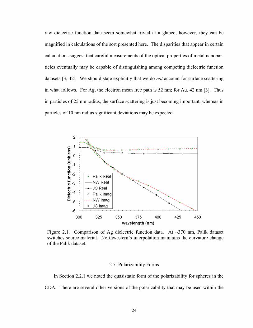
raw dielectric function data seem somewhat trivial at a glance; however, they can be
magnified in calculations of the sort presented here. The disparities that appear in certain
calculations suggest that careful measurements of the optical properties of metal nanopar-
ticles eventually may be capable of distinguishing among competing dielectric function
datasets [3, 42]. We should state explicitly that we do not account for surface scattering
in what follows. For Ag, the electron mean free path is 52 nm; for Au, 42 nm [3]. Thus
in particles of 25 nm radius, the surface scattering is just becoming important, whereas in
particles of 10 nm radius significant deviations may be expected.
Figure 2.1. Comparison of Ag dielectric function data. At ~370 nm, Palik dataset switches source material. Northwestern’s interpolation maintains the curvature change of the Palik dataset.
2.5 Polarizability Forms
In Section 2.2.1 we noted the quasistatic form of the polarizability for spheres in the
CDA. There are several other versions of the polarizability that may be used within the
24
basic formalism, depending on particle shape and the desired model. We now give an
overview of these expressions.
MLWA. The QSA is a severe limitation when calculating the optical properties of
spheres. Specifically, it ignores any spectral size-dependence of the resonance (other
than scaling with volume). For sufficiently large particles it is necessary to adjust the
particle polarizabilities to take into account two factors: 1) radiative damping, i.e. the ef-
fect of the reradiated field on the particle plasmon behavior, and 2) dynamic depolariza-
tion, caused by the finite ratio of particle size to wavelength (so that the QSA does not
strictly hold). The resulting modifications to the polarizability constitute the modified
long wavelength approximation (MLWA). First we write a more general form of the po-
larizability:
FL
Vmm
m
)( εεεεε
α−+
−= , (2.10)
where mε is the dielectric function of the surrounding medium, is a shape factor = 1/3
for spheres, and within the QSA
L
1=F . To apply the MLWA we set
32 )(32)(1 kaikaFMLWA −−= ; (2.11)
Here is the sphere radius (for ellipsoids it should be replaced with the semi-axis of in-
terest). The second term corresponds to dynamic depolarization, the third to radiative
damping [7]. (NOTE: I have adopted the terminology used by the Northwestern group
but not their equations. In Ref. [33] an entirely different form of the spheroid polarizabil-
ity is found from that of Bohren and Huffman, and the expression for the MLWA is ac-
cordingly different. There are several such oddities in Northwestern’s published work.
Evidently they yield the same answers, but the derivations of the equations are murky and
a
25
occasionally contain typographical errors. At least one of their versions of Eq. 2.4 con-
tains an important sign error: the first minus sign on the right-hand side is incorrectly
written as a plus sign in Ref. [35]. We initially discovered this by carefully applying the
right-hand rule for the cross products.)
Mie Theory. Mie’s treatment of spheres leads to expressions for scattering coeffi-
cients that may be used to calculate measurable quantities like optical efficiencies and
cross-sections for single isolated particles. However, these coefficients may themselves
be incorporated into the coupled-dipole formalism; that is, an effective electric dipole
polarizability may be calculated from the first-order scattering coefficient, as demon-
strated by Doyle [43]. The Mie scattering coefficients a and b are written as n n
)()()()()()()()(
mxxxmxmmxxxmxma
nnnn
nnnnn ψξξψ
ψψψψ′−′′−′
= ,
)()()()()()()()(
mxxmxmxmxxmxmx
bnnnn
nnnnn ψξξψ
ψψψψ′−′′−′
= (2.12)
where nψ and nξ are Riccati-Bessel functions, is the relative refractive index of the
particle compared with the embedding medium, and
m
kax = is the size parameter. (The
Mie expressions for optical cross-sections include summations over from 1 to infinity.)
The Riccati-Bessel functions and their derivatives can be expressed in terms of Bessel
and Hankel functions (which MATLAB supports), or even more simply as combinations
of sine and cosine functions using identities found in Ref. [44] (p.445). The effective di-
pole polarizability is related to the scattering coefficient [43]:
n
1a
13
6 ak
idipoleπα = (2.13)
26
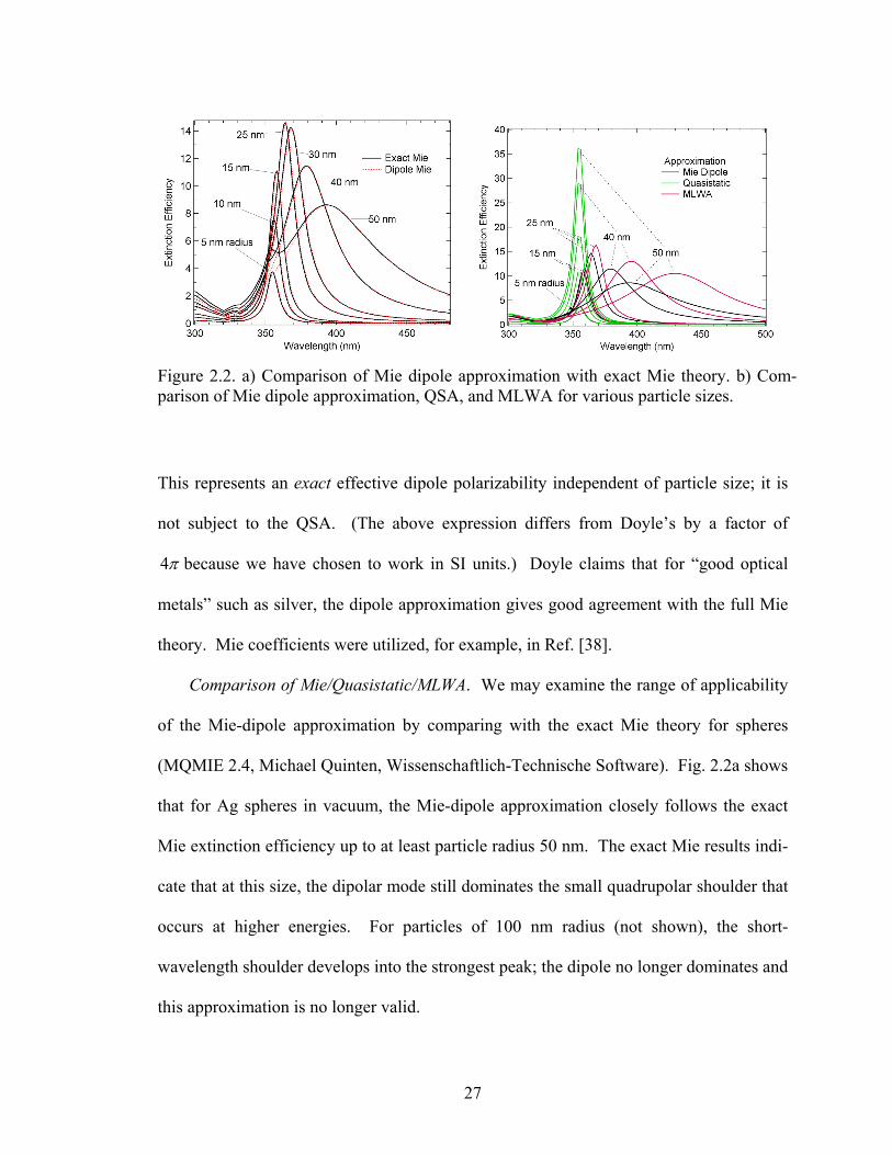
Figure 2.2. a) Comparison of Mie dipole approximation with exact Mie theory. b) Com-parison of Mie dipole approximation, QSA, and MLWA for various particle sizes.
This represents an exact effective dipole polarizability independent of particle size; it is
not subject to the QSA. (The above expression differs from Doyle’s by a factor of
π4 because we have chosen to work in SI units.) Doyle claims that for “good optical
metals” such as silver, the dipole approximation gives good agreement with the full Mie
theory. Mie coefficients were utilized, for example, in Ref. [38].
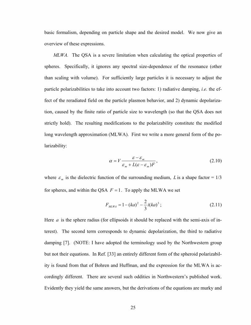
Comparison of Mie/Quasistatic/MLWA. We may examine the range of applicability
of the Mie-dipole approximation by comparing with the exact Mie theory for spheres
(MQMIE 2.4, Michael Quinten, Wissenschaftlich-Technische Software). Fig. 2.2a shows
that for Ag spheres in vacuum, the Mie-dipole approximation closely follows the exact
Mie extinction efficiency up to at least particle radius 50 nm. The exact Mie results indi-
cate that at this size, the dipolar mode still dominates the small quadrupolar shoulder that
occurs at higher energies. For particles of 100 nm radius (not shown), the short-
wavelength shoulder develops into the strongest peak; the dipole no longer dominates and
this approximation is no longer valid.
27

Fig. 2.2b demonstrates the size dependence of the QSA and MLWA compared with
the dipolar Mie model for Ag spheres. Clearly, the quasistatic spectrum is unchanged
with size, as expected from Eq. 2.2. For 5 nm radius, the correspondence with Mie the-
ory is exact. As size increases, the QSA becomes progressively worse. (Somewhat
ironically, the QSA works best where it works worst, because 5 nm radius in Ag is ap-
proximately where the real part of the dielectric function begins to depend strongly on
particle size [3].) The MLWA is a considerable improvement at intermediate sizes, as the
increased radiation damping with size is reflected in decreased amplitudes and the dy-
namic depolarization is seen in the redshift. However, at 40 nm radius, the redshift is ex-
aggerated by 20 nm, and for 50 nm radius by 40 nm. In light of the fact that the Mie di-
pole expressions may be programmed fairly readily (provided one is willing to wrangle
Riccati-Bessel functions) and do not appear to pose a significantly increased computa-
tional burden relative to the MLWA, it seems prudent to base any extinction calculations
for spheres on the Mie-dipole formalism. We should note that the MLWA appears to be
more useful for ellipsoids [33], for which exact computation schemes are much rarer,
though they do exist (see, e.g. [45]).
Ellipsoids. The general form of the polarizability for an ellipsoid in the quasistatic
approximation with semiaxes (not to be confused with the Mie coefficients) is
as follows:
cba ≥≥
)( mim
mi L
Vεεε
εεα
−+−
= (2.14)
The shape factors for the three possible axes obey the sum rule∑ . For
spheres the shape factors all collapse to
iL=
=3
11
iiL
3/1=iL , by which we arrive at Eq. 2.2. For ob-
28
late and prolate spheroids, analytical expressions of the shape factors may be found. We
list only the expression for an oblate spheroid, as it is a good approximation to a litho-
graphically-prepared disk.
2
)()(tan22
)( 21
21egeg
eegL −
−= −π ,
2
22 1
ace −= , 22
2
2
21)(ca
ce
eeg−
=−
= (2.15)
Here e is the eccentricity of the spheroid, where the limiting values are a disk (1) and a
sphere (0). For the oblate spheroid, 21 LL = .
The expressions for the shape factors of general ellipsoids are in integral form, as
follows (here ); cbai ,,=
∫∞
++++=
0 2222 ))()(()(2 qcqbqaqidqabcLi . (2.16)
However, the integrals may be solved straightforwardly in a few seconds using a
computer program like Mathematica. Because at this time MATLAB does not handle
infinities (or integrals in general) in a particularly natural way, Mathematica is greatly
preferred for this calculation. The shape factor integral calculations are extraordinarily
useful for calculating the linear optical properties of isolated metal nanoparticles, again
within the quasistatic approximation. Combined with the dielectric function of the mate-
rial, they can predict resonance peak positions for all three axes.
The results of shape factor calculations may be entered manually into a MATLAB
computation; this requires no additional programming labor if all particles are assumed
identical. It is worth noting that with a little effort, an array in which the individual parti-
29

cles have different isolated polarizabilities could be constructed and entered into the cal-
culation of self-consistent polarizabilities.
2.6 Does the Detector Make a Difference?
We now present results of CDA calculations with spheres. Our goal is twofold: to
demonstrate the effects of interparticle interactions on extinction spectra, and to test
whether a given detection geometry is correctly modeled by a simple efficiency calcula-
tion.
Figure 2.3. Extinction and scattering efficiencies for light normally incident on single 25 nm Ag sphere, compared with scattered power integrated over detector.
A check of the limiting behavior of the detector compared with an extinction effi-
ciency calculation in a traditional normal-incidence transmission or extinction measure-
ment demonstrates an important point. Strictly speaking, in the limit of zero solid angle,
the two calculations should coincide. Fig. 2.3 compares the extinction efficiency with
detector-integrated spectra for detector half-angles of 0.005° and 15°. We find for a sin-
30

gle 25-nm radius Ag particle that the integrated power is a decent approximation to the
extinction efficiency over a considerable range of acceptance angles. If we plot the scat-
tering efficiency, though, we find that the correspondence with the detector integration is
exact. This highlights the fact that the detector integration does not take account of ab-
sorption in the particle the same way that an extinction measurement does; the integration
only accounts for scattered light. In one sense this is as it should be; the detector should
only see differences in scattering, not absorption. Nonetheless, if the detector integration
is to model extinction measurements, the change in transmission due to absorption should
be accounted for in some way. Tabling that discussion for the present, we note that the
initial question now hinges on whether we can find differences between scattering effi-
ciency and detector response, and point out that scattering dominates absorption in the
limit of large particles. In any case, we have shown that for a single particle at normal
incidence the simple extinction efficiency is a near-perfect model for an extinction meas-
urement over an appreciable range of real detector angles, and the detector computation is
essentially superfluous.
Figure 2.4. Comparison of scattering efficiency and detector integration for light nor-mally incident on 5 x 5 square array of 25 nm Ag spheres spaced 75 nm apart. a) 0.005° cone; b) 15° cone.
31
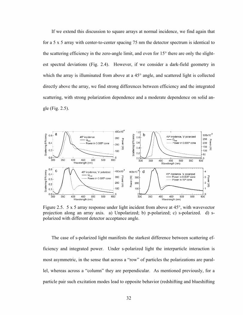
If we extend this discussion to square arrays at normal incidence, we find again that
for a 5 x 5 array with center-to-center spacing 75 nm the detector spectrum is identical to
the scattering efficiency in the zero-angle limit, and even for 15° there are only the slight-
est spectral deviations (Fig. 2.4). However, if we consider a dark-field geometry in
which the array is illuminated from above at a 45° angle, and scattered light is collected
directly above the array, we find strong differences between efficiency and the integrated
scattering, with strong polarization dependence and a moderate dependence on solid an-
gle (Fig. 2.5).
Figure 2.5. 5 x 5 array response under light incident from above at 45°, with wavevector projection along an array axis. a) Unpolarized; b) p-polarized; c) s-polarized. d) s-polarized with different detector acceptance angle.
The case of s-polarized light manifests the starkest difference between scattering ef-
ficiency and integrated power. Under s-polarized light the interparticle interaction is
most asymmetric, in the sense that across a “row” of particles the polarizations are paral-
lel, whereas across a “column” they are perpendicular. As mentioned previously, for a
particle pair such excitation modes lead to opposite behavior (redshifting and blueshifting
32
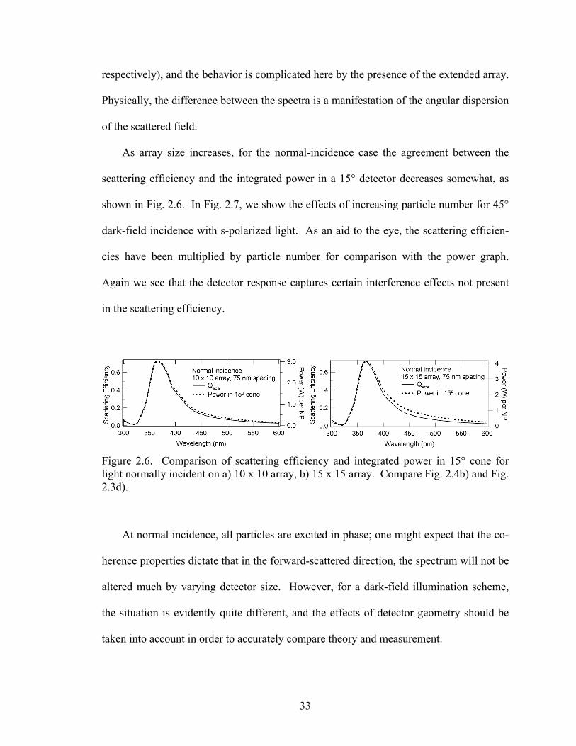
respectively), and the behavior is complicated here by the presence of the extended array.
Physically, the difference between the spectra is a manifestation of the angular dispersion
of the scattered field.
As array size increases, for the normal-incidence case the agreement between the
scattering efficiency and the integrated power in a 15° detector decreases somewhat, as
shown in Fig. 2.6. In Fig. 2.7, we show the effects of increasing particle number for 45°
dark-field incidence with s-polarized light. As an aid to the eye, the scattering efficien-
cies have been multiplied by particle number for comparison with the power graph.
Again we see that the detector response captures certain interference effects not present
in the scattering efficiency.
Figure 2.6. Comparison of scattering efficiency and integrated power in 15° cone for light normally incident on a) 10 x 10 array, b) 15 x 15 array. Compare Fig. 2.4b) and Fig. 2.3d).
At normal incidence, all particles are excited in phase; one might expect that the co-
herence properties dictate that in the forward-scattered direction, the spectrum will not be
altered much by varying detector size. However, for a dark-field illumination scheme,
the situation is evidently quite different, and the effects of detector geometry should be
taken into account in order to accurately compare theory and measurement.
33

Figure 2.7. Comparison of a) scattering efficiencies and b) integrated power for varying particle number at 45° incidence. Scattering efficiencies are multiplied by the number of particles in the array as a visual aid.
34
CHAPTER III
EXPERIMENTAL TECHNIQUES
Nanoparticle arrays were prepared with focused-ion-beam lithography; various
methods of structural characterization were employed. The ultrafast laser is briefly de-
scribed. The angle-resolved confocal fiber microscope used to measure scattering at arbi-
trary azimuthal angle is discussed in detail, and alignment procedures are given.
3.1 Focused Ion Beam Lithography
All nanoparticle arrays in this work were fabricated with Focused Ion Beam (FIB)
lithography (IBL) [46]. IBL is similar to electron-beam lithography (EBL) as described
in the literature for nanoparticle preparation [8, 13, 47].
Lithographic methods all follow a similar general procedure. The desired substrate
is coated with a thin layer of photoresist. The resist layer is exposed with an energized
beam which may consist of photons, electrons or ions. The exposure sites determine ei-
ther the final deposited image or its negative; resists are classified accordingly as “posi-
tive” or “negative”. In this work the positive photoresist poly(methyl methacrylate)
(PMMA) was used exclusively, as it is a common resist whose properties are relatively
well-known, particularly for EBL. The exposed parts of the resist may be removed by
chemical means. The remaining patterned resist is then coated with the desired material
by any of several thin-film deposition techniques. After coating, the resist layer is re-
35
moved entirely in a chemical bath such as acetone. Deposited material atop the resist
layer is removed as well, leaving behind the exposed image in the deposited material.
Substrates. Nearly all substrates used in this work were indium-tin-oxide(ITO)-
coated glass slides (Delta Technologies CB-90IN-0105, having 15-30 nm thick ITO
layer). The ITO is conductive enough to suppress charging during exposure and later im-
aging, yet sufficiently transparent (optical density OD less than 0.1 throughout the visi-
ble) to measure transmission and/or scattering in optical experiments. As received the
slides were 25 mm x 25 mm squares; for processing ease we divided them into quarters
measuring approximately 11 x 11 mm after cutting.
The ITO substrates are thoroughly cleaned before resist deposition. A typical proce-
dure is to rinse the substrate in consecutive 30-40 mL baths of acetone (Fisher Acros,
electronics use grade), methanol (Fisher Acros, electronics use grade), and de-ionized
water. The rinses are then repeated, this time using a cotton swab submerged in the ace-
tone and methanol baths to scrub the substrate clean, generally starting in the center of
the substrate and sweeping outwards. Any further spot-cleaning is determined by exami-
nation of the substrate reflectance under room lights with the naked eye. Such a simple
procedure is sufficient to achieve a clean surface with excellent resist coating characteris-
tics, as confirmed by imaging during exposure. Substrates are blown dry with clean dry
air (CDA).
Photoresist Preparation. A thin layer of PMMA photoresist is then spincoated onto
the clean substrate. All films in this work were made from solutions of PMMA in anisole
(Microchem 950 PMMA A4, 4% in anisole, diluted with Anisole 99%, Acros). We have
found experimentally that diluting the solution to ~1.7% yields PMMA thicknesses in the
36
range of 55-60 nm. The vacuum chuck on the spin processor used in this work (Laurel
WS-400A-6NPP/Lite) permits sample diameters as small as 1 cm; however, smaller sam-
ples may be accommodated by coating the opening with carbon tape and placing the
sample on the tape. The resist solution is applied to the mounted sample with a pipette
through an opening in the lid; at most 4 or 5 drops are required to coat a 1 cm x 1 cm
sample. The standard spinning procedure (per Microchem recommendations) is to spin
the sample at 500 rpm for 5 seconds to spread the solution over the entire sample, and
then spin at 4000 rpm for 45 seconds to make a thin layer. The carbon tape mounting
method will withstand 4000 rpm. The spun sample is then baked on a digital hotplate at
180° C for 60-90 seconds.
PMMA solution and film freshness is an important factor in film quality. A good
rule of thumb to follow is “the sooner, the better”. It is inadvisable to use PMMA films
that are more than a few weeks old in any case. PMMA solutions, especially diluted so-
lutions, should not be trusted for more than a couple of months without being tested by,
e.g., ellipsometry. Dilute solutions that have sat idle for any length of time should be
thoroughly mixed before use as the solute will settle. The best results are usually
achieved when films are made with fresh solution and used within 24 hours of prepara-
tion.
FIB Exposure. Resist exposure is performed with a commercial focused ion beam
apparatus (FEI FIB200) having a 30 kV source of Ga+ ions and a nominal beam diameter
of 8 nm when properly focused. The FIB computer interface allows the user to define the
sites to be exposed, and the exposure or dwell time at each site; thus arrays of arbitrary
complexity may be patterned to the specifications of the researcher. The final array size
37
depends upon the working magnification of the FIB. On the FIB200, a magnification of
3675 X is calibrated so that the resolution is 20 nm/pixel and the final array size is ~75
µm square. Dwell time does not appear to be a critical parameter, provided that film
thickness is in the 55-60 nm range; equivalent results have been obtained for identical
array patterns prepared with 60 µs to 100 µs dwell time on the same sample. However, if
the film thickness is larger, 100 µs is usually the safest time. The nominal beam current
used in all experiments is 1 pA; however, the actual measured values according to the
FIB picoammeter range from 2-4 pA.
Resist Development. Following exposure, samples were developed in a 1:3 solution
of methyl isobutyl ketone (MIBK, Acros AC32792) to isopropanol (IPA, Acros
AC32793) to remove the exposed regions of the resist. The 1:3 ratio is recommended by
the PMMA manufacturer (Microchem) as yielding the highest resolution images. Vari-
ous development procedures have been tested; the one that appears to yield the most con-
sistent results is as follows. Two beakers containing ~40 mL and a third containing ~15
mL of the 1:3 solution are prepared. The sample is bathed for 30 seconds with gentle agi-
tation in each of the first two solutions consecutively. The sample is then rinsed by pi-
pette for ~30 seconds over the second beaker, using fresh solution from the third; the en-
tire process takes 90 seconds. Following the development, the substrate should be gently
blown dry with CDA, then “hard-baked” on a digital hotplate at 100° C for 90 seconds.
The hard-bake is an important step, as it removes any remaining solvent in the patterned
regions.
38
Thin-Film Deposition. The developed sample is then coated with a layer of metal of
the desired thickness.§ The coating may be done by any of several processes, of which
this work employed two – Pulsed Laser Deposition (PLD) and thermal evaporation.
A commercial pulsed laser deposition system (Epion PLD 3000) was used in this
work. In PLD, a tightly-focused laser beam ablates a target; the ejected material is col-
lected on the substrate. The laser is a KrF excimer (Lambda-Physik Compex 205) with
wavelength 248 nm. The laser energy is set to 400 mJ with a repetition rate of 25 Hz. A
beamsplitter can be inserted into the optical path to divert ~50% of the light to a power
meter. The meter reading is typically 0.5 W, giving a time-averaged power of ~40 mJ
delivered to the target. From burn paper measurements of the spot size we estimate that
~70% of the beam energy is deposited into an approximately elliptical spot with axes 4
mm x 0.5 mm for an area of ~1.5 mm2; thus the peak fluence at the target is approxi-
mately 2±1 J/cm2, the error dominated by the measurement of the spot size. The PLD
vacuum chamber pressure is below 1 x 10⁻⁵ Torr. The target-sample distance is 7 cm.
Both target and sample are rotated (0.5-1 Hz) and the laser beam is rastered across the
target to ensure uniform deposition. Prior to each deposition the target is cleaned with
~104 laser pulses to remove any surface contamination. PLD of noble metals is a slow
process. Depending on laser power, about 50,000 to 80,000 pulses (30-50 minutes at 25
Hz) are required to produce a 20-nm thick film of silver at 7 cm. In crude approximation,
this indicates that ~ 600-1000 pulses are required to generate a monolayer of Ag at this
distance. Mass thickness is determined ex situ by spectrophotometric measurement of the
silver film thickness on a cover slide co-deposited with the sample. § The coating, of course, need not be metallic. Any material whose processing is compatible with the resist layer may be used, and in fact other researchers at Vanderbilt have used FIB lithography to create arrays of metal oxide nanoparticles such as vanadium dioxide and sesquioxide via pulsed laser deposition [48].
39
Thermal evaporation was performed in a Denton Vacuum DV-502A evaporator. In
thermal evaporation, large currents cause resistive heating, which evaporates the metal.
Tungsten coiled-wire baskets suspended between two electrodes hold the metal shot. The
distance between the basket and the sample is ~ 15 cm. Typical base vacuum pressure is
2 x 10⁻⁶ Torr. Typical currents needed to evaporate gold are of the order 30 A. Evapora-
tion is a fast process for noble metals, with typical maximum deposition rates 0.5-1
nm/sec; the deposition rate may be controlled in real-time by controlling the current.
Mass thickness may be monitored in situ with a quartz crystal microbalance (QCM);
however, a cover slide is always co-deposited with the sample as a second check. Due to
the different placements of the sample and the QCM, the QCM reading is typically 3/2 of
the actual deposited thickness. This has been confirmed by measuring distances in the
chamber, and by spectrophotometer tests. As the desired thickness is reached, the rate
may be slowed by reducing the current, and a mechanical shutter may be used to abruptly
stop deposition on the sample. The use of a custom sample holder which protects the
sample edges from deposition improves the ease of the liftoff process.
Liftoff. Liftoff of the lithographic mask is performed by immersion in a bath of
commercial solvent (Shipley Microposit 1165 Remover, or Remover PG) heated above
55° C. In general I have found that the bath should be heated to at least 57° C, and that
hotter is usually better. Recently, good results have been consistently achieved using
bath temperatures above 60° C. After the film has lifted off, the sample is rinsed in warm
acetone and DI water baths and blown dry with CDA. Examples of nanoparticle arrays
we have produced with IBL are shown in Fig. 3.1.
40

Figure 3.1. Scanning electron micrographs of Ag nanoparticle arrays produced by IBL. Scale bar in all frames is 1 µm.
Choice of Film Thickness. The range of 30 kV Ga+ ions in PMMA may be calcu-
lated using the freeware SRIM/TRIM program to be about 50 ± 10 nm. This places a
fundamental limit on the PMMA film thickness; for films thicker than 50 nm, only the
tail of the ion distribution penetrates the entire film. The desired thickness of the depos-
ited features places a lower limit on the resist thickness. Thinner metal films are easier to
lift off for at least two reasons: 1) the lower the ratio between the metal film thickness
and the resist thickness, the lower the probability that mechanical connections will form
between the metal in the hole and the metal atop the resist; and 2) very thin metal films as
deposited by PLD and evaporation are not truly solid; they have a porous structure which
41

the liftoff solvent can penetrate, dissolving the resist more easily. Mechanical connec-
tions would cause the particles to lift off along with the resist layer; they are minimized
when the angle between the trajectory of arriving atoms and the substrate normal is zero,
i.e. when fewer atoms have a chance to collect on the sidewalls. The porous metal-film
structure is readily observed in scanning electron micrographs. The object, then, is to use
the maximum resist thickness which can be thoroughly exposed within a 100 µs dwell
time. Resist thickness of 55-60 nm appears to be the best compromise.
Ga+ Contamination. For 80 µs dwell time at a beam current of 3 pA, about 1500
Ga+ ions are used to expose each site. Thus even if all Ga+ ions remain on an exposure
site after development (a highly unlikely situation), the maximum possible contamination
in a 60 nm diameter, 20 nm height Ag cylinder (containing more than 3 x 10⁶ atoms) is
less than 0.05%. Therefore, although bulk Ga is known to have an absorption peak be-
tween 500-600 nm, its effects on optical spectra of noble metal nanoparticles prepared by
FIB lithography should be negligible.
Comparison with EBL. IBL was used for the simple reason that an appropriate e-
beam writer was not available at Vanderbilt during this research. During the years we
have used IBL, some advantages of EBL have become apparent:
1. The penetration depth of electrons in PMMA is hundreds of nm; thus EBL
does not suffer the resist thickness constraint inherent to IBL.
2. Whereas only 103 ions are used to expose a site, some 105 electrons are typi-
cally used. Better statistics yields smoother edges of exposed regions.
3. With EBL, some fine control over particle diameter is possible, as demon-
strated by Gotschy et al. [8]. Increasing the electron dose yields larger di-
42

ameters. This has not yet been shown with IBL, and could be difficult to do
because increasing the FIB dose significantly would increase milling effects
which we wish to avoid. For doses between 60 and 120 µs (an admittedly
narrow exposure range), we have not observed significant particle size dif-
ferences. Changing the focus of the beam has a greater chance to affect par-
ticle size, but this is usually inadvisable for technical reasons. Stigmation in
the FIB is known to give skewed particle shapes, and defocusing likely
would have a similar effect on the size.
4. No Ga+ contamination is preferable to any contamination, however minimal.
5. In IBL the FIB is pushed to its lower limits of exposure; the instrument is
not optimal for this application.
6. The FIB is primarily a milling tool, and as such the heavy ions used could
conceivably alter the underlying substrate morphology.
7. FIB systems generally require a mechanical stage with eucentric rotation ca-
pability for milling purposes. EBL systems do not have this requirement;
hence they are more amenable to interferometric stage controllers, which al-
low fine control over the “stitching” or alignment of adjacent patterns.
Those points notwithstanding, IBL has proven to be quite satisfactory in constructing
nanoparticle arrays. Scanning electron microscopy (SEM) images of IBL nanoparticles
compare favorably with many literature images of nanoparticles of various shapes pre-
pared by EBL.
Furthermore, the fact that the FIB is best used as a milling tool gives IBL one sig-
nificant potential advantage over EBL. As nanoscale fabrication methods progress, it
43
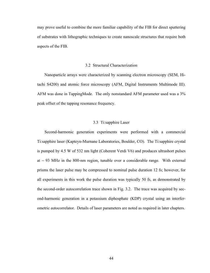
may prove useful to combine the more familiar capability of the FIB for direct sputtering
of substrates with lithographic techniques to create nanoscale structures that require both
aspects of the FIB.
3.2 Structural Characterization
Nanoparticle arrays were characterized by scanning electron microscopy (SEM, Hi-
tachi S4200) and atomic force microscopy (AFM, Digital Instruments Multimode III).
AFM was done in TappingMode. The only nonstandard AFM parameter used was a 3%
peak offset of the tapping resonance frequency.
3.3 Ti:sapphire Laser
Second-harmonic generation experiments were performed with a commercial
Ti:sapphire laser (Kapteyn-Murnane Laboratories, Boulder, CO). The Ti:sapphire crystal
is pumped by 4.5 W of 532 nm light (Coherent Verdi V6) and produces ultrashort pulses
at ~ 93 MHz in the 800-nm region, tunable over a considerable range. With external
prisms the laser pulse may be compressed to nominal pulse duration 12 fs; however, for
all experiments in this work the pulse duration was typically 50 fs, as demonstrated by
the second-order autocorrelation trace shown in Fig. 3.2. The trace was acquired by sec-
ond-harmonic generation in a potassium diphosphate (KDP) crystal using an interfer-
ometric autocorrelator. Details of laser parameters are noted as required in later chapters.
44
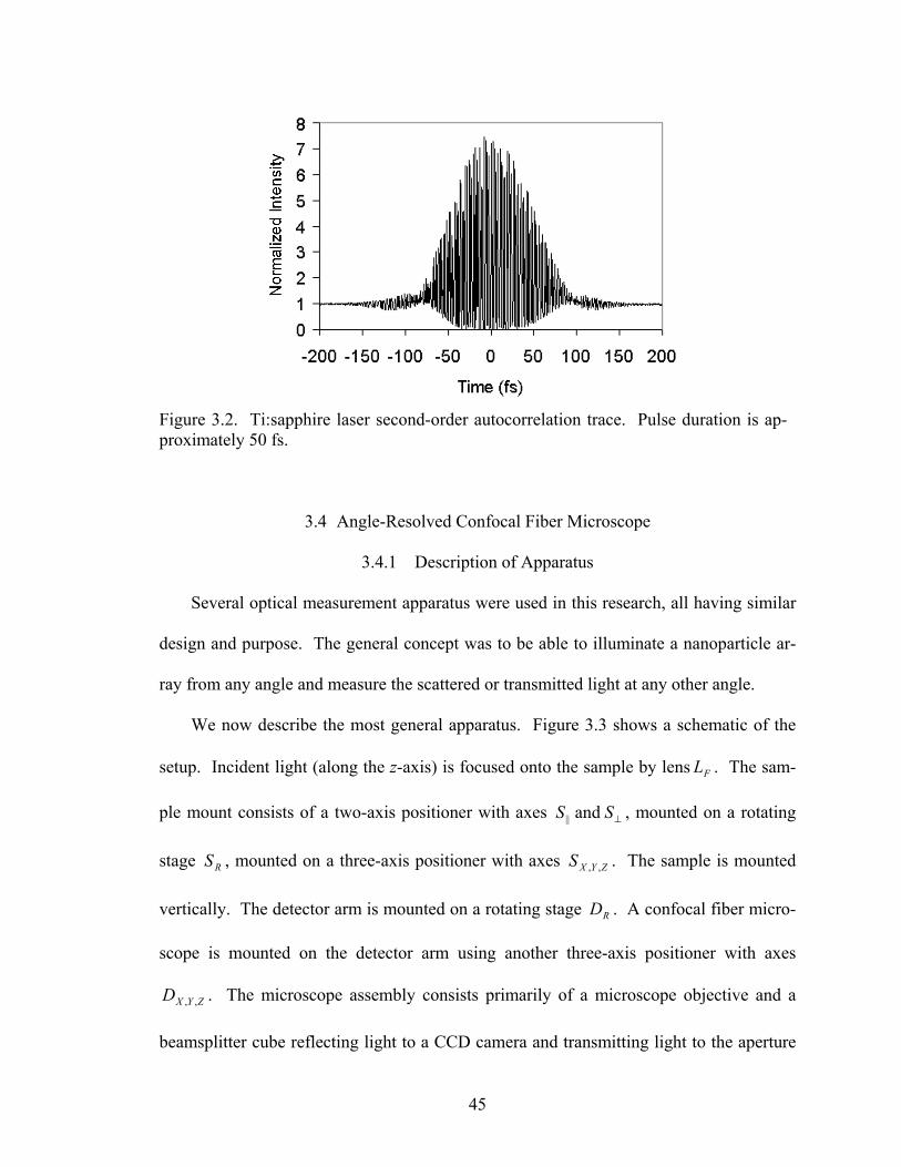
Figure 3.2. Ti:sapphire laser second-order autocorrelation trace. Pulse duration is ap-proximately 50 fs.
3.4 Angle-Resolved Confocal Fiber Microscope
3.4.1 Description of Apparatus
Several optical measurement apparatus were used in this research, all having similar
design and purpose. The general concept was to be able to illuminate a nanoparticle ar-
ray from any angle and measure the scattered or transmitted light at any other angle.
We now describe the most general apparatus. Figure 3.3 shows a schematic of the
setup. Incident light (along the z-axis) is focused onto the sample by lens . The sam-
ple mount consists of a two-axis positioner with axes , mounted on a rotating
stage , mounted on a three-axis positioner with axes . The sample is mounted
vertically. The detector arm is mounted on a rotating stage . A confocal fiber micro-
scope is mounted on the detector arm using another three-axis positioner with axes
. The microscope assembly consists primarily of a microscope objective and a
beamsplitter cube reflecting light to a CCD camera and transmitting light to the aperture
FL
⊥SS and ||
ZYXS ,,
RD
RS
ZYXD ,,
45

Figure 3.3: Schematic of dual-angle optical measurement system, top view.
of an optical fiber. Between the objective lens and the beamsplitter cube various optical
components may be placed (irises, pinholes, filters, polarizers) as needed.
Variations on this design will be described in the experimental details.
3.4.2 Alignment Procedures
The alignment of any system with so many adjustment micrometers is necessarily
complicated. The rotating stages , which are not mechanically coupled in any
way, must have their axes of rotation aligned to better than ~50 µm (i.e. the size of an
array). The laser beam must also intersect the two axes in a point, again to better than 50
µm. In this section we describe the alignment procedure for the system.
RR DS and
The substrate and detector rotation angles Sθ and Dθ are defined with respect to the
z-axis (incident light wavevector). °= 0Sθ when the sample normal points along the +z-
46
axis; in this orientation the light enters from the rear of the substrate. °= 0Dθ when the
detector directly faces the incident light. With this convention, DS θθ = signifies that the
detector is oriented normal to the substrate.
The alignment steps are as follows:
1. Before beginning sample stage alignment, the laser b i-
ly aligned to intersect the .
2.
eam and the detector m
rotation axis of
S is rastered abou
the camera or a p
= 9D
amera creen
crometers should be approximate RD
Laser alignment is aided by appropriately placed irises.
⊥S must first be aligned so that the sample plane intersects the sample rotation axis
RS . ⊥S should be adjusted at °= 0Dθ such that when θ t 0°, the
sam
ray a . Note
3.
ple region of interest (ROI) is not laterally displaced. (The ROI can be an ar-
or random substrate flaw) that the alignment array should be centered
in the camera.
XS may then be approximately aligned by setting °= 90Sθ and adjusting XS so
that the laser beam grazes the surface, as observed with iece of
paper. ZD (the detector focus) may then be aligned a °t 0θ .
Returning to °4. == 0DS θθ , align ZS until the sample is in focus. At this step, the
ROI should be in focus and centered on the sc for both
°°== and 0DS 90 θθ . If
rotation
it is not his indicates that XD is misaligned (provided
that ⊥S has been adjusted properly) such that the microscope is not pointing at the
RD .
, t
true center of
47
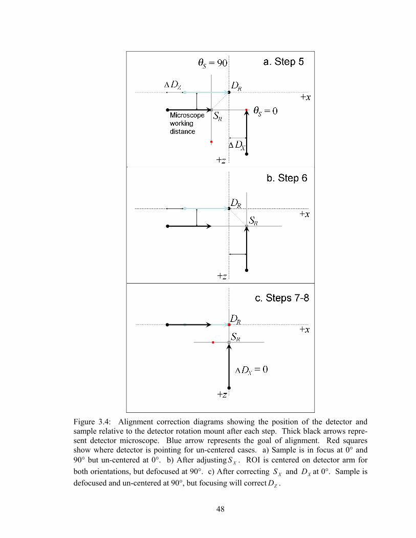
48
X
X X
Z
Figure 3.4: Alignment correction diagrams showing the position of the detector and sample relative to the detector rotation mount after each step. Thick black arrows repre-sent detector microscope. Blue arrow represents the goal of alignment. Red squares show where detector is pointing for un-centered cases. a) Sample is in focus at 0° and 90° but un-centered at 0°. b) After adjusting S . ROI is centered on detector arm for both orientations, but defocused at 90°. c) After correcting S and D at 0°. Sample is defocused and un-centered at 90°, but focusing will correct D .
5. To correct : First, adjust and so that the sample is in focus at both
0° and 90°, but the ROI is not centered in one orientation (see Figure 3.4a for
symptom diagram). Note the micrometer positions.
XD ZX SS , ZD
6. By adjusting either or , one can make the ROI appear centered in both ori-
entations, but in one orientation it will appear unfocused (see Figure 3.4b for
symptom diagram). Note the new position for the micrometer that was moved.
XS ZS
7. In both cases (steps 5 and 6) the are both wrong; but, conveniently, they are
wrong by the same amount. In step 6, for example, the chosen micrometer was
moved exactly to the opposite side of the correct position. Calculate the correct
position (midway between the two recorded points) and move the micrometer
there. That micrometer should now be in the correct position.
ZXS ,
8. should then be adjusted by the same amount (and direction) as the micrometer
in step 7. Now is correct. (See Fig. 3.4c.)
XD
XD
9. Switch to the other orientation and adjust until the sample is in focus (although
the ROI will not be centered); the adjustment should be the same distance as the
other steps.
ZD
10. Switch back to the first orientation and “focus” with the remaining . Again,
the adjustment should be the same distance as the others. At this point the align-
ment should be very close to correct, and fine-tuning may be done iteratively fol-
lowing the algorithm of steps 5-9.
ZXS ,
11. It may prove necessary to realign the laser at this point.
49

When the system is fully aligned, the sample may be moved in its own plane by the
micrometers and (horizontal and vertical respectively.) In an ideal world, the only
regular adjustment necessary would be , when mounting a new sample. The reader
may judge for himself whether we live in an ideal world.
||S YS
⊥S
50
CHAPTER IV
RAPID TARNISHING OF Ag NANOPARTICLES
Chemical activity in silver nanoparticles exposed to laboratory air can make interpre-
tation of optical scattering and extinction spectra problematic. We have measured the
shift of the plasmon polariton frequency of arrays of silver nanoparticles with increasing
exposure to ambient laboratory air. The resonance peak wavelength shifts 65 nm in 36
hours (1.8 nm/hr). We show by scanning Auger spectroscopy that the shift is due to con-
tamination from sulfur, most likely chemisorbed on the surface. The rate of corrosion
product growth on the nanoparticles is estimated to be 3 nm per day, 7.5 times higher
than that of bulk Ag under the same conditions.**
4.1 Introduction
The LSPR of silver nanoparticles is stronger than that of the other noble metals, and
has its peak amplitude in vacuum at a higher frequency [3]. The former characteristic
makes silver an ideal candidate for use in applications that exploit the plasmon-polariton
resonance. The latter uniquely qualifies silver nanoparticles to respond in the violet re-
gion of the visible spectrum, since the Mie resonances [2] of gold and copper particles
typically appear in the green and red regions and most deviations from the ideal case of
spherical particles in vacuum result in a redshift of the SPP wavelength. In addition, sil-
ver has strong interband transitions in the visible, and thus is an excellent material for
studying the interplay between single-electron and multi-electron excitations (e.g. inter- ** The content of this chapter has already been published in Applied Physics B, 2005 [49].
51

band transitions and SPPs) [50]. However, the utility of silver for nanophotonics applica-
tions is compromised by its lack of chemical stability in ambient conditions, leading to
damping of the resonance by multiple mechanisms, such as dielectric damping and
chemical interface damping (CID) [51, 52].
Silver is widely known to corrode or tarnish in air [53-57], and sensitivity to gas ex-
posure has been measured [58] and explored for gas sensors [59]. Surprisingly, thus far
there has been no systematic study of simple corrosion effects on silver nanoparticles in
the laboratory environment [A. Leitner, personal communication]. In this chapter we
present measurements of the optical shift of the plasmon resonance peak in lithographi-
cally-prepared arrays of silver nanoparticles with increasing exposure to laboratory air.
We demonstrate by scanning Auger spectroscopy that this optical shift is due to chemi-
sorbed sulfur on the nanoparticles. We estimate the rate of corrosion in the silver
nanoparticles using our optical data along with optical constants of silver sulfide from the
literature [53] and reasonable physical assumptions.
4.2 Experimental Methods
The ordered arrays of silver nanoparticles used for these experiments were fabricated
using IBL as described in Chapter III. Silver was deposited by PLD. In this work all ar-
rays had particles arranged in a 2D square lattice unless otherwise stated. Array size was
typically 60 x 60 µm2; particle diameter was typically 60-70 nm. Following liftoff, the
samples were stored in small wafer carriers (Entegris 1” single wafer shippers) having a
capacity of about 1 cm3. The wafer carriers have a screw-tight cover that provides a good
seal.
52
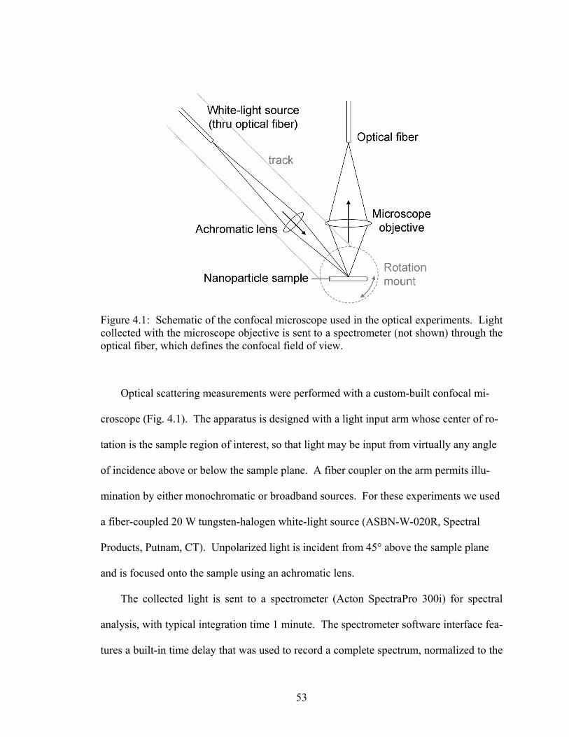
Figure 4.1: Schematic of the confocal microscope used in the optical experiments. Light collected with the microscope objective is sent to a spectrometer (not shown) through the optical fiber, which defines the confocal field of view.
Optical scattering measurements were performed with a custom-built confocal mi-
croscope (Fig. 4.1). The apparatus is designed with a light input arm whose center of ro-
tation is the sample region of interest, so that light may be input from virtually any angle
of incidence above or below the sample plane. A fiber coupler on the arm permits illu-
mination by either monochromatic or broadband sources. For these experiments we used
a fiber-coupled 20 W tungsten-halogen white-light source (ASBN-W-020R, Spectral
Products, Putnam, CT). Unpolarized light is incident from 45° above the sample plane
and is focused onto the sample using an achromatic lens.
The collected light is sent to a spectrometer (Acton SpectraPro 300i) for spectral
analysis, with typical integration time 1 minute. The spectrometer software interface fea-
tures a built-in time delay that was used to record a complete spectrum, normalized to the
53

output of the lamp, every 15 minutes over a time span ranging from hours to days for dif-
ferent arrays. The raw spectra were smoothed using an adjacent-averaging smoothing
routine in the data analysis software (Origin); the number of adjacent data points used for
averaging varied from 25 to 50 for different spectra.
Auger microanalysis of some of the arrays was performed at the High Temperature
Materials Laboratory at Oak Ridge National Laboratory, using a Phi 680 Scanning Auger
Nanoprobe. The primary electron beam was provided by a field emission source oper-
ated at a beam energy of 20kV and beam current of 10nA. This probe beam was focused
to a spot size of ~20nm and the Auger electrons emitted from the sample were detected
using a cylindrical mirror analyzer. Electron micrographs were obtained at Vanderbilt
University using a Hitachi S4200 Scanning Electron Microscope equipped with a cold
field emission electron gun.
4.3 Results
Fig. 4.2 shows the change in the optical response as a function of exposure to labora-
tory air for a 2D square array of annealed silver nanodisks (20 nm height, 60 nm diame-
ter) with grating constant 162 nm. Fig. 4.2a shows selected spectra from a series that was
taken every 15 minutes over a period of 36 hours. The redshift, broadening and weaken-
ing of the resonance over time are clearly demonstrated. The peak amplitude decreases
nearly one order of magnitude. In Fig. 4.2b the resonance peak wavelength position as a
function of time is plotted. The resonance position redshifted 65 nm in 36 hours nearly
linearly, giving a shifting rate of ~1.8 nm/hr.
54

Figure 4.2: (a) Selected SPP spectra from an array of silver nanoparticles with increasing exposure to laboratory air. (b) Redshift of the resonance peak with increasing exposure. Shifting rate is 1.8 nm/hr. Grating constant of array is 162 nm.
55

Figure 4.3: SPP resonance shift. Note that the resonance position after removal from storage is comparable to the initial resonance of the array in Fig. 4.2b even though this sample is 2 days older. Shifting rate is 1.25 nm/hr. Grating constant of array is 147 nm.
We observed that arrays sharing a particular grating constant on samples that were
stored in the 1” wafer carriers always seemed to have approximately the same initial
resonance position immediately after being removed from the carriers, independent of the
time spent in storage. Once placed on the microscope stage (open to ambient), however,
the arrays began to shift dramatically. Fig. 4.3 shows the shift of one such array (not an-
nealed, grating constant 147 nm) left in storage for 2 days before being placed on the mi-
croscope stage. Here the shift is less dramatic but still pronounced (~1.25 nm/hr). The
initial resonance position is similar to the array in Fig. 4.2 although the delay between
sample preparation and optical characterization was much larger.
A capping layer of dielectric material (200 nm, PMMA) prevented any further shift
in the optical properties over an appreciable period. Fig. 4.4 demonstrates that spectra
56

Figure 4.4: Effect of dielectric coating. Spectra were taken from the same PMMA-coated array on consecutive days with 19 hours elapsed between spectra. Spectra have been smoothed with adjacent-averaging process. The resonance position, amplitude and width were preserved.
taken from the same capped array on successive days had virtually identical peak position
and line shape.
The results of Auger spectroscopy of silver nanoparticles exposed to ambient are
shown in Fig.4.5. The nanoparticle “dimer” shown in Fig. 4.5a constitutes a basis set of a
larger 2D lattice structure fabricated by IBL. The Auger spectrum reveals the presence of
sulfur on the silver nanoparticle. The indium, tin and oxygen signals are reduced at the
nanoparticle locations because the measuring technique is highly surface-sensitive.
There is a slight increase in the carbon peak at the nanoparticle.
Over the time intervals given in Figs. 4.2 and 4.3, the nanoparticles do not change
their shape significantly. Fig. 4.6 shows electron micrographs of a region of an array (a)
57

Figure 4.5: (a) Electron micrograph of Ag nanoparticle “dimer” analyzed with Auger spectroscopy. (b) Auger spectra of regions indicated in (a). Sulfur is found with silver on the particle.
58
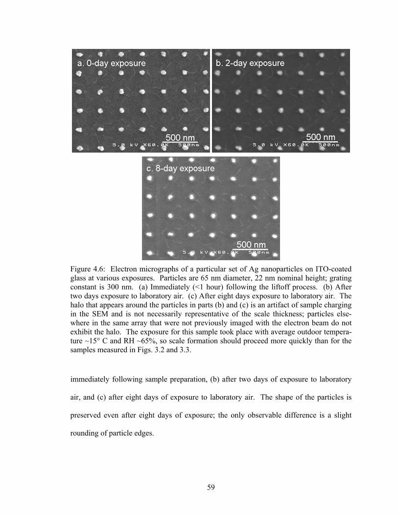
Figure 4.6: Electron micrographs of a particular set of Ag nanoparticles on ITO-coated glass at various exposures. Particles are 65 nm diameter, 22 nm nominal height; grating constant is 300 nm. (a) Immediately (<1 hour) following the liftoff process. (b) After two days exposure to laboratory air. (c) After eight days exposure to laboratory air. The halo that appears around the particles in parts (b) and (c) is an artifact of sample charging in the SEM and is not necessarily representative of the scale thickness; particles else-where in the same array that were not previously imaged with the electron beam do not exhibit the halo. The exposure for this sample took place with average outdoor tempera-ture ~15° C and RH ~65%, so scale formation should proceed more quickly than for the samples measured in Figs. 3.2 and 3.3.
immediately following sample preparation, (b) after two days of exposure to laboratory
air, and (c) after eight days of exposure to laboratory air. The shape of the particles is
preserved even after eight days of exposure; the only observable difference is a slight
rounding of particle edges.
59
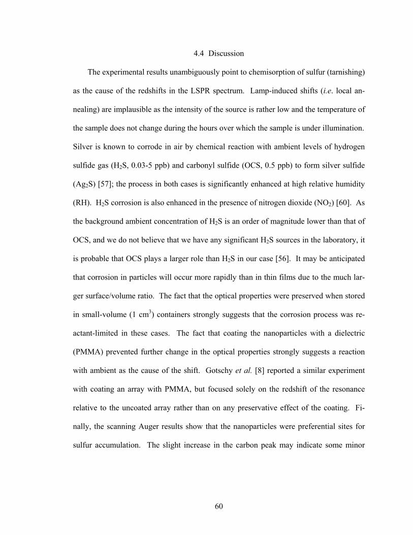
4.4 Discussion
The experimental results unambiguously point to chemisorption of sulfur (tarnishing)
as the cause of the redshifts in the LSPR spectrum. Lamp-induced shifts (i.e. local an-
nealing) are implausible as the intensity of the source is rather low and the temperature of
the sample does not change during the hours over which the sample is under illumination.
Silver is known to corrode in air by chemical reaction with ambient levels of hydrogen
sulfide gas (H2S, 0.03-5 ppb) and carbonyl sulfide (OCS, 0.5 ppb) to form silver sulfide
(Ag2S) [57]; the process in both cases is significantly enhanced at high relative humidity
(RH). H2S corrosion is also enhanced in the presence of nitrogen dioxide (NO2) [60]. As
the background ambient concentration of H2S is an order of magnitude lower than that of
OCS, and we do not believe that we have any significant H2S sources in the laboratory, it
is probable that OCS plays a larger role than H2S in our case [56]. It may be anticipated
that corrosion in particles will occur more rapidly than in thin films due to the much lar-
ger surface/volume ratio. The fact that the optical properties were preserved when stored
in small-volume (1 cm3) containers strongly suggests that the corrosion process was re-
actant-limited in these cases. The fact that coating the nanoparticles with a dielectric
(PMMA) prevented further change in the optical properties strongly suggests a reaction
with ambient as the cause of the shift. Gotschy et al. [8] reported a similar experiment
with coating an array with PMMA, but focused solely on the redshift of the resonance
relative to the uncoated array rather than on any preservative effect of the coating. Fi-
nally, the scanning Auger results show that the nanoparticles were preferential sites for
sulfur accumulation. The slight increase in the carbon peak may indicate some minor
60
Figure 4.7: Calculated extinction efficiencies, in the quasistatic approximation, of sur-face-parallel and surface-normal modes of oblate Ag spheroid (height 2c = 20 nm, di-ameter 2a = 60 nm), embedded in vacuum ( )1=ε and an effective medium taking ac-count of the substrate ( )3.2=ε (as parameterized for the nearly identical sample geome-try in [8]). ‘A’ refers to surface-parallel mode, ‘C’ to surface-normal mode.
preferential hydrocarbon adsorption; it may alternately indicate the presence of PMMA
fragments left over from the development and lift-off processes.
Our particles are best approximated as oblate spheroids. Oblate spheroids in general
exhibit two resonances: a surface-parallel mode with two symmetric components, and a
surface-normal mode. We observe only one peak in our spectra; this corresponds to the
surface-parallel mode. For an oblate spheroid having height 20 nm and diameter 60 nm,
embedded in an effective medium having 3.2=ε [8], the surface-normal mode may be
calculated (using the quasistatic approximation) to occur at ~350 nm, as demonstrated in
Fig. 4.7. The surface-parallel mode occurs at ~500 nm, consistent with our observations.
The much weaker surface-normal mode was not in the range of the spectrometer for these
experiments. We also note that since we illuminate at 45° with unpolarized light, only
about a fourth of the incident light is coupled to the surface-normal mode to begin with.
61
Changing the nanoparticle interface from silver/air to silver/silver sulfide “scale” of
increasing thickness results in redshift and damping of the resonance. A Mie calculation
(MQMIE 2.4, Michael Quinten, Wissenschaftlich-technische Software) of the scattering
of Ag spheres coated with a shell of varying thickness of Ag2S demonstrates this qualita-
tively, and we may draw some limited quantitative bounds from it as well. The Mie cal-
culation makes some obvious but serious approximations. Among other assumptions,
particles are modeled as non-interacting spheres in air rather than interacting oblate sphe-
roids on a supporting substrate; step-function boundaries between the various dielectric
spatial regions are assumed, which is certainly not the case in our experiment; and
chemical interface damping (CID), which represents an additional damping mechanism
beyond the simple dielectric damping of the Mie model, is neglected entirely. Nev-
ertheless, we can simulate the experimental trends sufficiently to make the sulfidation
argument plausible.
Fig. 4.8a shows the scattering efficiency for Ag spheres of 25 nm initial radius. We
make the simplifying assumption that a given outer shell thickness of Ag reacts com-
pletely to form the Ag2S scale. Optical constants for Ag are taken from Johnson and
Christy [40]; optical constants for Ag2S are taken from Bennett et al. [53]. Due to the
difference in density between Ag (10.5 g/cm3) and its sulfide (7.2 g/cm3) [61], the corre-
sponding scale thickness is significantly (~50%) larger than the original thickness of Ag
that reacted to form the scale. For example, for an initial particle radius of 25 nm, a con-
version of 1 nm Ag results in a scale layer of 1.6 nm (the correspondence with increasing
shell thickness is very slightly sub-linear). The amplitude of the scattering efficiency is
very sensitive to the increasing scale thickness; hence the log-linear plot in part a).
62

Figure 4.8: Calculated Mie scattering efficiency of Ag spheres with Ag2S shells of vary-ing thickness, in air. Spheres are initially 25 nm radius pure Ag; the corroded shell is assumed to be completely converted to Ag2S. Thickness values listed are prior to con-version (1 nm Ag → 1.6 nm Ag2S for a sphere of 25 nm initial radius). In part (a), ordi-nate is plotted on a log scale for clarity. Note different abscissa range in parts (a) and (b).
Notice that when 4 nm of Ag has corroded, a small dip in the peak appears around
450 nm; the dip becomes more pronounced with increasing scale thickness. We observe
no such feature in our spectra (compare Fig. 4.2a); this suggests an upper limit of order 6
nm of scale growth on our particles. In fact, the damping behavior in our data is more
closely mimicked by much smaller scale thicknesses ≤1.6 nm, as shown in Fig. 4.8b).
63
Our results show behavior similar to the data presented by Stanford on discontinuous
thin Ag2S layers grown in laboratory ambient on roughened evaporated Ag films [54].
Stanford notes that, because the real part of the dielectric function of both Ag and Ag2S is
nearly linear with respect to wavelength in the 300 to 500 nm region, the resonance peak
wavelength should shift nearly linearly with increasing thickness for small thicknesses.
This result seems to be applicable in the nanoparticle case as well according to the Mie
calculation above, although the ratio of the SPP shift to the sulfide thickness increase is
much larger in the nanoparticle case as one might expect. Our results indeed show a lin-
ear relation between total exposure and wavelength shift; this suggests that for our parti-
cles the average scale thickness increased linearly with total exposure over the time inter-
vals analyzed.
A linear increase of sulfide thickness with exposure is consistent with an initial flux-
limited growth phase that, at least in the case of H2S exposure of bulk Ag, extends
through the formation of ten equivalent monolayers (ML) of scale [56]. Since OCS re-
sults in approximately the same (usually slightly smaller) scale thickness as H2S for simi-
lar exposures, we may safely assume that the sulfide thickness of our nanoparticles is less
than ten ML (~5 nm) which corresponds to total exposure of ~1 ppm·hr. This mildly
constrains our previous limit. However, if we assume an OCS concentration of 0.5 ppb,
in 36 hours we arrive at a total exposure of ~18 ppb·hr. Even if we are near a source of
H2S, with concentration 5 ppb, the total exposure in 36 hours is 180 ppb·hr, still well
within the linear growth regime. Furthermore, the experiments in [57] were performed at
92% RH. Our experiments were performed in cold dry months when the indoor RH is
much lower. These considerations would place the upper limit of the scale thickness
64
much lower, at ≤1 nm. Nonetheless, this conclusion would only be accurate if the reac-
tivity of the silver nanoparticles is the same as that of bulk silver. Due to the high sur-
face-to-volume ratio, and the high curvature of the nanoparticle surface, we may expect
that the reaction rate is higher for our nanoparticles than for the samples in [57] (as well
as the samples in [55]). Since we are in the linear growth regime, we may use our data to
estimate the increase in reactivity for the nanoparticles relative to the bulk.
Fig. 4.8b shows the results of a Mie calculation converting up to 1 nm of an Ag
sphere of initial radius 25 nm to sulfide scale (scale thicknesses up to 1.6 nm). The peak
wavelength shift of 16 nm is much smaller than we measured here. Since the resonance
of Ag spheres blueshifts with decreasing radius to a minimum at ~15 nm, the redshift due
to the increased dielectric function of the surroundings is partly compensated by the
shrinking of the Ag core. (We note that, since our particles are on a supporting substrate
– the dielectric effects of which do not change with time – they are not surrounded by
scale; thus we would require in general a larger actual scale thickness to achieve the same
optical shift as for an imaginary particle which is symmetrically corroded.) A 3-nm-thick
shell of Ag converted to scale (4.7 nm Ag2S) would give an SPP shift of 54 nm, more
congruent with our data. We may compare our results to the work of Burge et al. [62]
which used samples similar to those of Stanford [54]. They reported H2S concentration
of <0.2 ppb, and under atmospheric conditions in their laboratory the Ag2S growth rate
was 0.4 nm per day and essentially linear over the time interval studied (8 days). Since
the resonance shift should be approximately linear with respect to thickness, using Fig.
4.2 data with the Mie calculation we estimate that 4.5 nm scale thickness grows in 1.5
days, giving a growth rate of 3 nm per day, which is 7.5 times higher than the thin film
65
case; low precision is warranted by the crudeness of our Mie model. Recent papers by
Haes et al. [10, 11] indicate that the resonance peak shift with increasing dielectric layer
thickness is larger in less spherical particles, so in modeling spheres we likely have over-
estimated the growth rate by 10-20%. The actual rate may be still lower depending on
the relative importance of the dielectric contribution to the SPP shift (compared to, e.g.,
CID effects).
The rate of corrosion is different for the data in Figs. 4.2 and 4.3. This is explained
by different RH during the two experiments. Archived hourly weather observations for
Nashville, TN (http://www.intellicast.com) indicate that the average outdoor RH during
collection of data in Fig. 4.2 was 68%, while that for Fig. 4.3 was 47%; in both cases out-
door temperatures were near freezing, so the percentages scale to room temperature in the
same way. Since all our shifts are in the linear regime, and the RH dependence is
roughly linear, this accounts for the difference in the shift (1.8/1.25 = 68/47).
Tarnishing of bulk silver is known to create “whiskers” of silver sulfide [55]. From
this fact we might expect that sulfidation could produce a distortion of nanoparticle
shape. Contrariwise, the electron micrographs of nanoparticle sulfidation in Fig. 4.6 indi-
cate that the exposures in these experiments do not cause significant particle deformation
– if anything, morphological changes tend toward a more circular profile. This elimi-
nates shape changes as an agent of optical redshift; indeed, any increased sphericity
would induce a slight blueshift and cause underestimation of the dielectric shift by coun-
tering its effect on the measured spectrum. We have not characterized the nanometer-
scale crystallinity of the particles under study (i.e., any porosity within the individual
nanoparticles which would increase the surface area, yielding an apparent increase in re-
66
activity). However, the PLD technique is a standard one used by many researchers for
creation of nanoparticles and gives results quite similar to evaporative deposition, so we
would not expect any significant structural differences between our particles and those of
other researchers. Furthermore, the similarity in behavior between the experiments and
the Mie calculations supports the qualitative assertion that the tarnishing occurs on the
surface of the particles. Thus we expect that researchers studying nanoparticles prepared
by similar techniques would measure reactivities similar to those presented here.
4.5 Conclusion
We have studied the chemical instability of silver nanoparticles under ambient condi-
tions. Relatively thin corrosion layers formed by reaction of silver nanoparticles with
atmospheric sulfurous compounds lead to significant changes in the optical response over
a period of days. The shifts due to tarnishing can be of the same order as shifts due to
variation of the grating constant, for example. The optical changes are primarily due to
the modification of the dielectric environment of the nanoparticles, with a slight cor-
rection to account for the shrinking Ag core; shape changes are relatively unimportant for
the particle types and exposures studied. In the linear growth regime, we may use the
optical shift to estimate the reactivity of the nanoparticles; the rate of corrosion in Ag
nanoparticles is several times higher than in the bulk and can be as high as 3 nm Ag2S per
day, even at low (~20%) indoor RH. The observed changes in the optical properties with
time should be representative of ambient conditions in most laboratories and may be used
as a benchmark.
67

CHAPTER V
PERSISTENCE OF GRATING EFFECTS IN ANNEALED Ag NANOPARTICLE ARRAYS
We measure the optical characteristics of ordered arrays of silver nanoparticles using
a frustrated-total-internal-reflection technique. Momentum conservation dictates that dif-
ferent wavelengths are dispersed at different angles, and the angular characteristics are
dependent upon the grating constant. The strength of the diffraction conditions is demon-
strated in a frustrated total-internal-reflection geometry using a nanoparticle array which
has been annealed to destroy the individual particle quality. The wide particle-size distri-
bution gives rise to extreme inhomogeneous broadening of the LSPR. The finite numeri-
cal aperture of the detector reveals the presence of strong diffraction by a cutoff wave-
length that depends upon the grating conditions.
5.1 Introduction
The concept driving the emerging field of nanophotonics is to use nanoscale features
to control photons, whose characteristic length scale is many times the size of the rele-
vant structural features. For instance, extensive research over the past decade sought to
exploit the possibility of using metal nanoparticle chains as photonic circuitry to localize
and propagate optical signals [63-65]. The dependence of the LSPR position and width
on nanoparticle spacing has also been studied using two-dimensional arrays and particle
pairs of gold and silver. Felidj and coworkers demonstrated that the position and width
of the LSPR for two-dimensional arrays of gold nanoparticles depends upon the lattice
68

constant of the array as well as the individual particle sizes [66]; Haynes and coworkers
also studied the array spacing dependence for gold and silver disk and trigonal prism ar-
rays [67]. Rechberger and coworkers studied the simpler case of pairs of gold nanoparti-
cles with separation ranging from touching to three diameters apart; they found good
agreement with a simple model of interacting dipoles [36]. Gunnarsson and coworkers
studied similar silver particle pairs and achieved similar results [37]. But ordered arrays
of noble metal nanoparticles provide a particularly interesting method of controlling light
not only because the LSPR varies with interparticle spacing, but also because the order
contributes strong spatial phase coherence. Put another way, the far-field coupling could
be as useful as the near-field coupling.
Some comparisons between near-field and far-field coupling have been explored.
Linden and co-workers have shown that coupling of array resonances to guided modes in
a dielectric waveguide results in enhanced transmission for certain wavelengths, depend-
ing on the array parameters [68]. Lamprecht and coworkers also investigated the effects
of far-field coupling on the plasmon dephasing time, showing that as successive dif-
fracted orders become allowed the radiative damping of the LSPR increases [14]. Still –
perhaps because the topic of diffraction gratings seems mundane – relatively little work
has been done to demonstrate or take advantage of the diffractive character of these two-
dimensional gratings as such. In this chapter we present a simple, explicit demonstration
of the diffractive character of metal nanoparticle arrays, and consider this as a method for
controlling light. In succeeding chapters we will consider ways to exploit the diffractive
character in the nonlinear intensity regime.
69
We have measured the optical response of two-dimensional arrays of silver nanopar-
ticles by a frustrated total internal reflection (FTIR) technique. Particularly when parti-
cles are small and spacings are large, it is difficult to achieve good signal in a traditional
normal-incidence extinction measurement. FTIR geometry improves the optical signal to
such an extent that the technique has been used to study the far-field optical spectra of
single nanoparticles [69]. The details of the FTIR measurement allow us to demonstrate
that the method by which light is re-radiated from the arrays into the previously forbidden
region is governed by the properties of the surrounding media. It also depends on two
other controllable experimental parameters: the angle of the incident light, and the ge-
ometry of the arrays.
5.2 Experimental Methods
Silver nanoparticle arrays were fabricated by IBL as described in Chapter III. Ag
was deposited by PLD to 20 nm mass thickness. In the annealing step, the sample was
annealed in the PLD vacuum chamber with a low pressure of argon gas at 350°C for 30
minutes.
We set up our FTIR experiment on the platform of a scanning near-field optical mi-
croscope (WITec AlphaSNOM) in a confocal arrangement (Fig. 5.1). The experiments
described in this chapter do not take advantage of the optical near-field measurement ca-
pabilities of the instrument, but we note that nothing in our setup precludes near-field
measurements with FTIR geometry. The sample is placed on a rhomboid glass prism
70
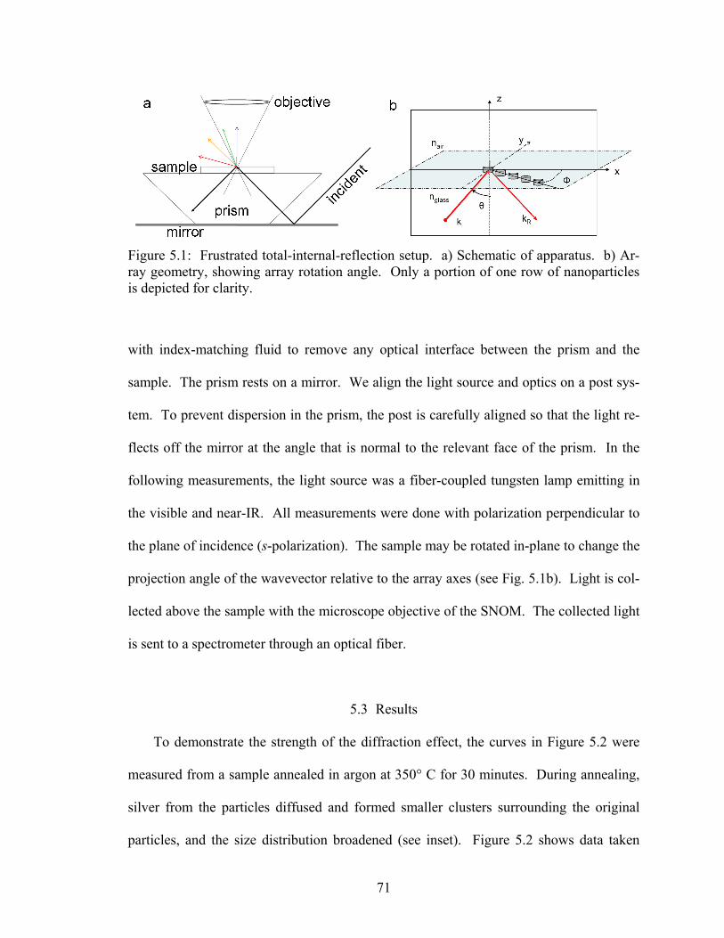
Figure 5.1: Frustrated total-internal-reflection setup. a) Schematic of apparatus. b) Ar-ray geometry, showing array rotation angle. Only a portion of one row of nanoparticles is depicted for clarity.
with index-matching fluid to remove any optical interface between the prism and the
sample. The prism rests on a mirror. We align the light source and optics on a post sys-
tem. To prevent dispersion in the prism, the post is carefully aligned so that the light re-
flects off the mirror at the angle that is normal to the relevant face of the prism. In the
following measurements, the light source was a fiber-coupled tungsten lamp emitting in
the visible and near-IR. All measurements were done with polarization perpendicular to
the plane of incidence (s-polarization). The sample may be rotated in-plane to change the
projection angle of the wavevector relative to the array axes (see Fig. 5.1b). Light is col-
lected above the sample with the microscope objective of the SNOM. The collected light
is sent to a spectrometer through an optical fiber.
5.3 Results
To demonstrate the strength of the diffraction effect, the curves in Figure 5.2 were
measured from a sample annealed in argon at 350° C for 30 minutes. During annealing,
silver from the particles diffused and formed smaller clusters surrounding the original
particles, and the size distribution broadened (see inset). Figure 5.2 shows data taken
71

Figure 5.2: TOP – Scattered spectra from several annealed particle arrays with different lattice constant. The light is collected with a microscope objective of numerical aperture 0.8 and normalized to the particle areal density and the spectral profile of the source.LOWER LEFT – Electron micrographs of array with 147 nm periodicity before and after 30 minute anneal in argon at 350° C. LOWER RIGHT – LSPR spectrum of non-annealed array with 147 nm period and silver nanoparticles with 60 nm diameter and 25 nm height, illuminated with white light at 45° from the normal; scattered light was col-lected in reflection mode (as in Chapter IV) with a NA = 0.25 lens normal to the array.
72
with the array aligned with the light projection along an axis, i.e. 0°. Similar measure-
ments were taken at 45° and 90° array rotation angles. Sharp cutoff wavelengths are ob-
served in the spectra at each rotation angle. In addition, we observe a broad resonance on
the low-wavelength side of the cutoffs.
5.4 Discussion
The boundary conditions on the electric and magnetic fields for light impinging on
an optical interface require that the x-components of the relevant wavevectors must be
equal,
xdtransmittexreflectedxincident kkk ,,, == . (4.1)
Ignoring for the moment the reflected wave, we may then write the components of
the wavevectors in terms of the vacuum wavevector k0,
xdtransmitteTIxincident kknknk ,0201, sinsin === θθ , (4.2)
which is easily recognized as a variant of Snell’s Law. The important point here is that
for a condition of total internal reflection 1sin >Tθ , so the x-component of the transmit-
ted wavevector is larger than the vacuum wavevector. Consulting the dispersion relation,
we see that this does not correspond to a radiative field in the second medium; the only
way to vectorially add the wavevector components to achieve an allowed (lightlike) total
wavevector is for the z-component to be imaginary, which in fact it is. This is the cause
of the exponential attenuation of the evanescent wave in the z direction. The condition
for a wavevector to be lightlike in a medium of refractive index is jn
0, kn k jxj ≤ . (4.3)
73
We require an explanation, then, for the observation that we detect light above the
sample. The transmitted wavevector, as we have shown, is too large to exist as light.
However, it can couple to plasmons in the particles in the array, which then can reradiate
the light. Since light is observed, there must be some shrinking of the wavevector that is
caused by the array. We may write the momentum conservation condition as
g(Lattice),, −= xdtransmittexshortened kk (4.4)
where g is some function dependent on the lattice parameters. Based on dimensional
symmetry and a familiar analogy with solid-state physics, we surmise that g is a recipro-
cal lattice vector of the form
a
m π2 g(Lattice) = , (4.5)
where a is the lattice constant of the array and m is an integer. (We consider the case in
which the array is aligned with the x-axis; the generalization to other array orientations in
the xy-plane is straightforward.) Noting that the x-components of the transmitted and in-
cident wavevectors are equal, we have
amnn IT π
λθπ
λθπ 2sin2sin2
0
1
0
2 += , (4.6)
or rearranging,
ann IT0
12 sinsin λθθ −= . (4.7)
Here we have chosen m to correspond to a shortening of the wavevector. This
equation implies that if we collect light above the sample with a collector having a nu-
merical aperture
1−=
sin max, 1NA <= Tθ , there will be certain wavelengths that will not be
collected.
74
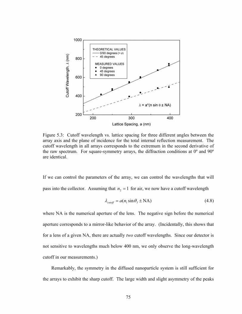
Figure 5.3: Cutoff wavelength vs. lattice spacing for three different angles between the array axis and the plane of incidence for the total internal reflection measurement. The cutoff wavelength in all arrays corresponds to the extremum in the second derivative of the raw spectrum. For square-symmetry arrays, the diffraction conditions at 0º and 90º are identical.
If we can control the parameters of the array, we can control the wavelengths that will
pass into the collector. Assuming that 12 =n
( 1
for air, we now have a cutoff wavelength
= na )NAsin ±Icutoff θλ (4.8)
where NA is the numerical aperture of the lens. The negative sign before the numerical
aperture corresponds to a mirror-like behavior of the array. (Incidentally, this shows that
for a lens of a given NA, there are actually two cutoff wavelengths. Since our detector is
not sensitive to wavelengths much below 400 nm, we only observe the long-wavelength
cutoff in our measurements.)
Remarkably, the symmetry in the diffused nanoparticle system is still sufficient for
the arrays to exhibit the sharp cutoff. The large width and slight asymmetry of the peaks
75
is attributed to the size distribution of the individual nanoparticles in the annealed sam-
ples. (For reference, Figure 5.2c is the LSPR spectrum of a non-annealed array, meas-
ured using a reflection technique. No cutoff is observed in that spectrum because the
grating constant is rather short and the incident and reflected wavevectors experience the
same refractive index.) Figure 5.3 shows that the cutoff wavelengths measured in the dif-
fused system (from the raw spectra) correspond precisely to the values calculated from
diffraction theory.
76

CHAPTER VI
DIFFRACTED SECOND HARMONIC GENERATION FROM Au NANOPARTICLE ARRAYS
We show that second-harmonic light can be generated from a diffraction grating of
gold nanoparticles with planar inversion symmetry. By measuring the angular distribu-
tion of second-harmonic light, we observe a novel effect in which the diffraction pattern
of the grating is superimposed on the intrinsic second-harmonic radiation pattern of the
nanoparticles. This result suggests that second-harmonic generation may be used to
study coherent nonlinear optical effects in symmetric as well as asymmetric metal
nanoparticles.††
6.1 Introduction
Second-harmonic generation (SHG) has been used for over two decades as an optical
probe of electronic properties of metal nanoparticles (NPs) of varying shape, size, com-
position and spatial organization [3, 16, 17, 71-78]. The objectives of metal NP studies
in general have ranged from measuring electron dephasing [71, 73, 79-83], to pinpointing
the origin of surface-enhanced Raman scattering [17, 84-86] and assessing the potential
for plasmonic applications such as all-optical switching [75, 87-89].
It is usually taken for granted that symmetry forbids the generation of second-
harmonic light in centrosymmetric NP systems [90]. Even when asymmetric NPs are ar-
ranged so that the overall array has inversion symmetry, SHG is completely suppressed
†† The content of this chapter has already been published in Physical Review B, 2006 [70] and was included in the AIP/APS Virtual Journal of Nanoscale Science and Technology (http://www.vjnano.org, 13, no. 3).
77

along the illumination direction [81]. This quenching of SHG along the illumination di-
rection holds true for both surface and bulk SHG contributions [72, 81, 82]; for this rea-
son, the potential of SHG for probing electron dynamics in metal NPs has generally been
discounted [83]. In this paper, we demonstrate that this difficulty is ameliorated simply
by looking at angles other than the illumination direction. This is the first measurement
of diffracted SH from NPs with such a high degree of symmetry.
Recently, it has been proposed that arranging asymmetric NPs in a diffraction grating
should provide spatial separation of NP-generated SH light from both the incident fun-
damental beam and the substrate-generated SH light [18], a technique first demonstrated
in the 1980s on asymmetric Ag NPs supported on an array of dielectric posts [17]. (From
the constructive interference condition λθ m=sin , odd-integer orders of the second har-
monic are equivalent to half-orders of the fundamental, so SH light appears where fun-
damental light does not. This principle has been used to study SHG from 1D diffraction
gratings of polymers [91], adsorbed dye molecules [92] and metals [93].) However,
asymmetric NPs are not strictly necessary. We report diffracted SHG from Au nanorods
of planar symmetry aligned in a symmetric two-dimensional grating, even when optically
excited in a symmetric manner. The resulting SH diffraction pattern is unique in that
virtually no zero-order peak exists, and the SHG intensity increases with diffracted order
for a single array (and generally with increasing angle of observation from the normal).
The SHG depends strongly on resonant enhancement between the particle plasmon reso-
nance and the excitation frequency.
78

6.2 Experimental Methods
Nanorod arrays were fabricated on indium-tin-oxide(ITO)-coated glass by IBL and
thermal evaporation as described in Chapter III. Au was evaporated over the polymer
mask to 20 nm mass thickness. Array integrity and NP structure were determined by
SEM (Fig. 6.1 inset). Minor defects in the IBL process gave rise to regions of irregular
particle coverage, but the arrays had excellent diffractive properties overall. We use
nanorods instead of nanodisks (which have higher symmetry) because the different axial
lengths in a rod give rise to different resonance energies; hence we may probe SHG on-
or off-resonance by rotating the array relative to the incident light. It is also technically
easier to control the resonance energy through rod length than through disk diameter.
Fig. 6.1 shows the detection apparatus. The NP arrays, typically 60x60 µm2, were
illuminated by a passively mode-locked Ti:sapphire resonator pumped by 4.5 W of 532
nm light; the oscillator produces 50-fs pulses with center wavelength 800 nm at 93 MHz
pulse-repetition frequency with average power ~250 mW. Residual green pump light
was blocked with a color filter. Power fluctuations were monitored by a silicon photodi-
ode. Pulse duration was measured with an autocorrelator. The fluence was sufficiently
low (<0.1 mJ/cm2) that SHG was achieved without modifying NP morphology. The lin-
ear extinction coefficients along the major and minor axes of the nanorods were deter-
mined separately with a white-light source and rotatable linear polarizer.
79

Figure 6.1: Experimental setup for measuring angular distribution of SH light. Inset: SEM image of “tilted” rods with 200 nm spacing.
A 5-cm focal length lens focused the fundamental beam to a ~50 µm diameter spot.
We employed the configuration of Zheludev et al. [18], in which the laser is normally
incident from the rear of the substrate. The arrays were aligned so that the incident po-
larization pointed along a grating axis. The nanorods pointed either along the grating
axis or at a 45° angle to it. The detector arm rotated in the plane defined by the funda-
mental propagation and polarization directions.
The detector optical train consisted of a microscope objective (NA 0.25), removable
filters, a beamsplitter cube for camera viewing, and an optical fiber to direct the light ei-
ther to a spectrometer with a Peltier-cooled CCD array or a photomultiplier tube (PMT)
connected to a photon counting module. For PMT measurements, the SH was filtered by
a monochromator set to pass 400 nm, assuring the spectral purity of the signal. At each
observation angle the PMT signal was optimized; where multiple measurements were
acquired at an angle, the highest recorded value is plotted. In the figures, the relative er-
ror is plotted, representing the standard deviation of ten consecutive measurements. Due
to difficult alignment the absolute uncertainty could be substantially higher.
80
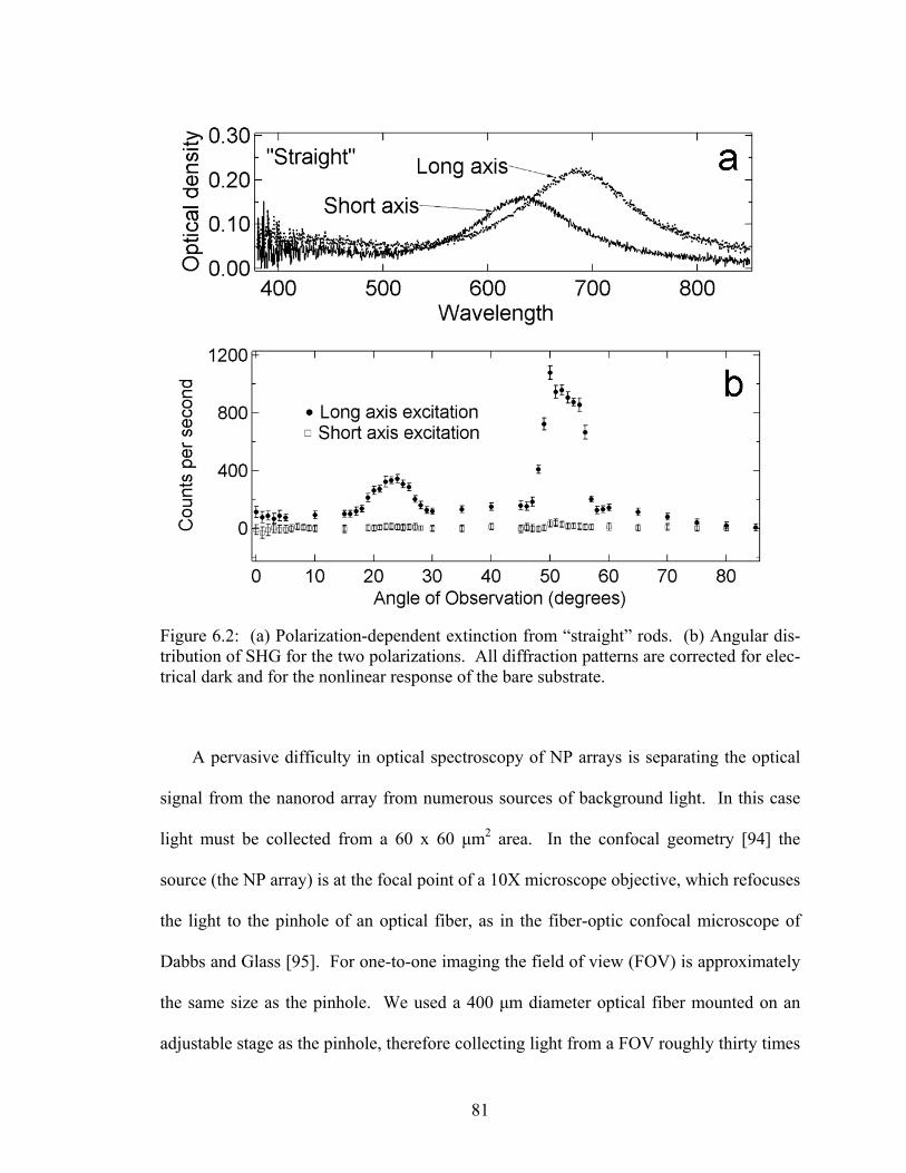
Figure 6.2: (a) Polarization-dependent extinction from “straight” rods. (b) Angular dis-tribution of SHG for the two polarizations. All diffraction patterns are corrected for elec-trical dark and for the nonlinear response of the bare substrate.
A pervasive difficulty in optical spectroscopy of NP arrays is separating the optical
signal from the nanorod array from numerous sources of background light. In this case
light must be collected from a 60 x 60 µm2 area. In the confocal geometry [94] the
source (the NP array) is at the focal point of a 10X microscope objective, which refocuses
the light to the pinhole of an optical fiber, as in the fiber-optic confocal microscope of
Dabbs and Glass [95]. For one-to-one imaging the field of view (FOV) is approximately
the same size as the pinhole. We used a 400 µm diameter optical fiber mounted on an
adjustable stage as the pinhole, therefore collecting light from a FOV roughly thirty times
81

Figure 6.3: (a) Polarization-dependent extinction from “tilted” rods. (b) Angular distri-bution of SHG with varying lattice spacing. The signal from the 600-nm-spacing array is scaled by 0.36 to match the areal density of the 1-µm-spacing array.
the area of the NP array. While using a relatively large pinhole diminished the achiev-
able signal-to-noise, it provided some flexibility in the alignment.
6.3 Results
Figure 6.2 shows the angular distribution of SH light from a 1-µm grating of Au
nanorods aligned along the grating axes. The SH output from the long axis is greatly en-
hanced relative to the short axis because the linear extinction of the long axis is nearly
82
triple that of the short axis at the excitation wavelength of 800 nm. In the resonant case,
the diffracted peak amplitudes are reversed from the conventional situation.
Angular distributions for SH light diffracted by “tilted” rods at NP spacings of 600
nm and 1 µm, respectively, are plotted in Figure 6.3. When normalized to NP areal den-
sity, patterns from the two arrays display a general trend of increasing peak intensity with
increasing observation angle. These rods are longer than those of Fig. 6.2; thus they ex-
hibit greater extinction (in the long-axis mode) than the “straight” rods at the excitation
wavelength of 800 nm. This is why although the particle orientation with respect to the
laser is not optimal, the SH output is comparable to the straight-rod case.
At an observation angle of 0°, we observe no SH light except a small and easily iden-
tified background that appears in the absence of the arrays. This spurious signal is
probably generated at the collection objective by the incident beam, and is generally
weaker than the diffracted SH peaks. The first diffracted order of fundamental light is a
tiny fraction of the incident beam, so it likely lacks the intensity to produce spurious SH.
Thus, even though the second diffracted order of the SH coincides with the first dif-
fracted order of the fundamental, we are confident that we observe only SHG from the
NP array at all orders.
6.4 Discussion
The angular distribution in a given measurement is the superposition of the radiation
pattern from an individual NP with the diffraction pattern dictated by the array geometry.
By adjusting the grating constant, we select the emission angle; in this way we may re-
produce the overall angular distribution from the individual nanorods with high sensitiv-
83
ity due to constructive interference. In all cases we observe no forward-scattered SH
light from the NPs, as expected from the symmetry of the array.
Several possible mechanisms may give rise to the observed radiation patterns. In the
case of isolated centrosymmetric spheres, such a pattern can be produced either by 1) SH
dipole emission generated in a nonlocal process involving both volume and surface sus-
ceptibilities of the NPs; or 2) SH quadrupole emission in a local process involving only
surface susceptibilities [96]. Either mechanism could be effective in our particles. How-
ever, in our particular case the rods are supported on a substrate, so the dielectric envi-
ronment is asymmetric perpendicular to the substrate with air above and ITO below.
This configuration could potentially generate SH even without these more complex
mechanisms, since there is a nonzero effective second-order susceptibility (due to the
broken symmetry) of the form . The data presented in Fig. 6.3 are insufficient to
judge whether there is a quadrupolar component of the SH emission pattern; quadrupolar
components could be distinguished at angles
)2(||||⊥χ
θ such that3 , i.e. at angles be-
yond 55°.
1)(cos2 >θ
A simple model of resonant enhancement and SH diffraction gives qualitative agree-
ment with our results. In this model, SH light is generated from an effective dipole SH
source that itself varies as the square of the local fundamental field (LFF); thus the SH
intensity goes as the fourth power of the LFF, which arises from the response of the ellip-
soid to the incident electric field. We caution that this model does not account for multi-
polar excitations that may indeed be present in particles of the size examined here, and
we have further assumed that the induced SH source is purely dipolar and perpendicular
to the substrate (i.e. out-of-plane) without reference to any nonlinear susceptibilities.
84

Still, the main features of the experiment – diffraction and resonant enhancement – are
reproduced rather well, indicating that the model incorporates most of the essential phys-
ics. In addition, although the particles are ~100 nm in the lateral dimensions (which may
give rise to quadrupole effects), their height is only 20 nm; thus for the excitation geome-
try we used, retardation effects should be small since h/λ ~ 1/40 [97].
The nanorods may be loosely approximated by general ellipsoids. Using a plane wave
approximation for the incident light with the foregoing approximations, we may write the
induced LFF along an axis of the nanorod (normalized to the incident field) as follows
[4]:
)(
)(1
11
21
10
1
mjm
mjj
LL
EE
εεεεε
ε −+−
−
−= , (5.17)
with indices zyxj ,,=
jL
corresponding to ellipsoid semiaxes respectively. The
shape factors may be written as integrals and computed numerically; for example,
cba ≥≥
∫∞
++++=
02222 ))()(()(2 qcqbqaqa
dqabcLx . (5.18)
It is instructive to note that, for wavelengths near resonance, the ratio between the LFFs
for the x and y axes reduces to
−−
−−
=
xm
ym
y
x
L
L
EE
11
11
1
1
1
1
εε
εε
. (5.19)
When the numerator and denominator of the RHS are set equal to zero, we obtain the sur-
face plasmon resonance condition for general ellipsoids [4].
85

Due to the planar fabrication method, the NPs are not strictly ellipsoidal. However, if
we assume a fixed particle height 2c = 20 nm, the extinction maxima of Fig. 6.2a can be
approximated by an ellipsoid of dimensions 2a = 90 nm, 2b = 78 nm. These parameters
were used to calculate the ratio of SH intensities for the major and minor axes, plotted in
Fig. 6.4a. Assuming a purely dipolar SH radiation pattern varying with angle as sine-
squared, we have modeled Figs. 6.2b and 6.3b using the equations [98]
θβθαθαα
ββθ sin
2,sin
2,sin
sinsinsin)( 212
22ll kkN
NI ≡≡
∝ (5.20)
where is the number of NPs in a row, is the wavenumber, and and l are the grat-
ing spacing and NP size respectively. The results, plotted in Fig. 6.4, agree reasonably
with our experiments. The intrinsic width of the peaks, which is approximately 1°, is not
resolved in our experiments due to a relatively large numerical aperture.
N k 1l 2
The individual particles have considerable substructure common to lithographic NPs,
as evidenced by the SEM image. Local field enhancement can be substantial at nano-
scale roughness features, giving rise to enhanced nonlinearities, so the roughness defects
may be considered SH sources [99]. In addition, deviations from ideal NP shapes have
been linked to optical activity particularly in SHG patterns [100]. However, the observed
SH diffraction pattern specifies that such defects may not radiate constructively in the
forward direction. The data suggest that roughness defects are distributed more or less
randomly on the NPs, and our excitation geometry and detection scheme are insensitive
to the tensor components discussed in Ref. [100], so we observe no shape bias. There is a
small “noise” SH signal at most angles, as seen in Fig. 6.2 (especially for the resonant
86
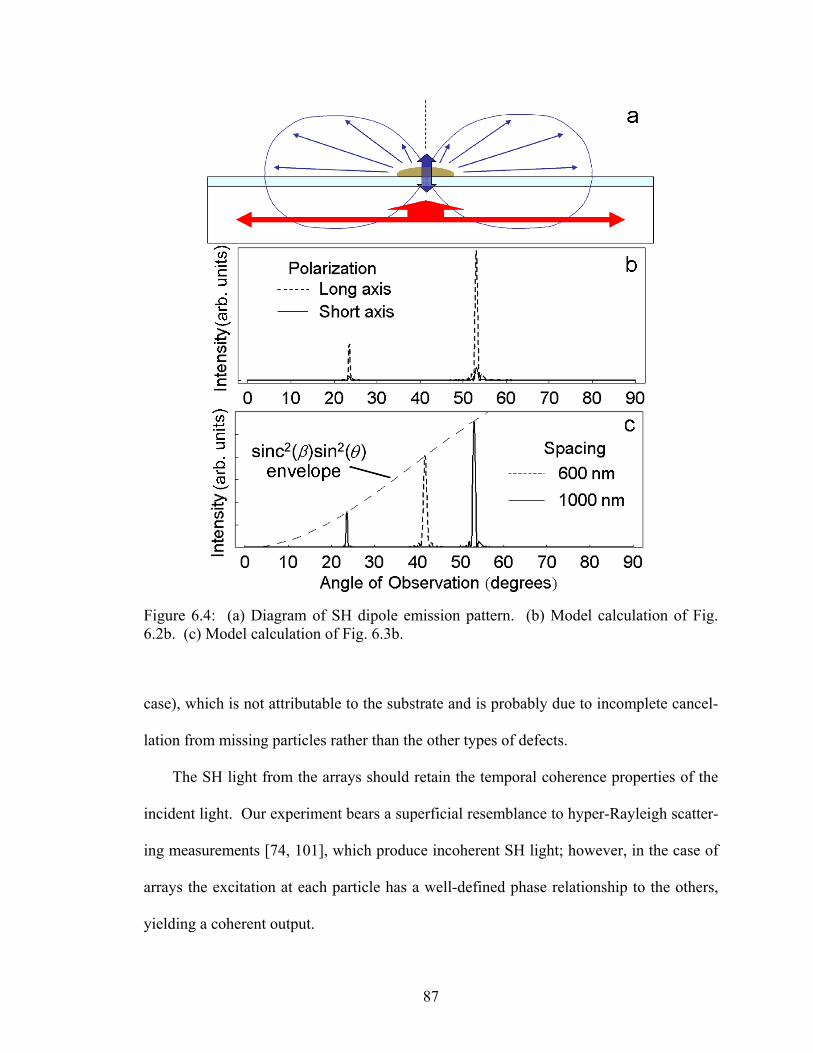
Figure 6.4: (a) Diagram of SH dipole emission pattern. (b) Model calculation of Fig. 6.2b. (c) Model calculation of Fig. 6.3b.
case), which is not attributable to the substrate and is probably due to incomplete cancel-
lation from missing particles rather than the other types of defects.
The SH light from the arrays should retain the temporal coherence properties of the
incident light. Our experiment bears a superficial resemblance to hyper-Rayleigh scatter-
ing measurements [74, 101], which produce incoherent SH light; however, in the case of
arrays the excitation at each particle has a well-defined phase relationship to the others,
yielding a coherent output.
87
The scheme used here differs from that of Ref. [18] in that the NPs we studied have
in-plane symmetry. We note that angular measurements on asymmetric particles would
retain the out-of-plane SH contribution, while exhibiting an additional in-plane contribu-
tion due to individual NP asymmetry. This is not explicitly accounted for in Ref. [18],
and could complicate the interpretation of such experiments because the proportion of the
out-of-plane contribution would depend on the diffracted angle and hence on the grating
spacing. Specifically, the prediction that the ratio of the first-order SH peak to the first-
order fundamental peak depends only on the particle structure is called into question.
6.5 Conclusion
This experiment demonstrates that SH may be produced and directed by an appropri-
ately designed grating using symmetric particles, avoiding complications in both lithog-
raphy and interpretation.
88
CHAPTER VII
RESONANTLY ENHANCED SECOND HARMONIC GENERATION FROM Au NANOPARTICLE ARRAYS
SHG from lithographically prepared arrays of symmetric gold nanorods can be in-
creased by two orders of magnitude by choosing nanoparticle size to be resonant with the
800-nm wavelength of the pump laser. The angular variation of the second-harmonic
yield, which is defined by the pitch of the nanorod array, can be predicted using standard
diffraction theory. This in turn makes it possible to bound approximately the relative
contributions of dipole and quadrupole oscillations to the total second-harmonic yield.
Resonant ultrafast irradiation also induces morphological changes in the nanorods, a re-
shaping that apparently results from surface melting and refreezing of the nanorods. At
higher fluence, the intensity dependence of the second-harmonic yield changes from
quadratic to cubic, an indication that the reshaping influences the mechanism of SHG.‡‡
7.1 Introduction
Second-harmonic generation (SHG) is a particularly surface-sensitive optical probe
[78]. Metal nanoparticles, with their large optical resonances and high surface-to-volume
ratio, would seem to be excellent substrates for measurements that require surface sensi-
tivity. Thus, SHG from metal nanoparticles is of potentially great importance. SHG
studies of lithographic arrays of the simplest nanoparticle shapes (disks) have met obsta-
cles because symmetry constraints forbid SHG in the forward and backward directions
[96, 101]. To circumvent this problem, some researchers have turned to asymmetric par- ‡‡ The content of this chapter has been submitted for publication to Applied Physics B.
89
ticle shapes [81, 102] or to third-order methods [83]. However, we have shown that it is
possible to observe SHG from symmetric nanoparticles arranged in a diffraction grating
even when illuminated in a symmetric geometry. Because of the symmetry constraints,
one must look at nonzero azimuthal angles to observe it. This method avoids the extreme
sensitivity of radiated SH light to even small changes in asymmetric particle shape [75,
103], and allows us to excite and detect in the near-visible spectral region. It also ac-
cesses different tensor components of the second-order susceptibility than those probed
for asymmetric particle shapes like triangles or L-shaped particles. Furthermore, the op-
tical properties of symmetric nanoparticles are much easier to calculate [4], aiding com-
parison of theory with experiment.
Ordering the NPs in an array is crucial, because the phase-matching condition pro-
vided by the grating structure greatly improves the signal-to-noise ratio [18]. In Chapter
6 we used arrays of NPs which were weakly resonant with the excitation wavelength.
Here we present results from arrays of NPs whose extinction maxima are well-matched to
the laser wavelength, improving the signal by orders of magnitude. By varying the grat-
ing constant for a particular NP shape, we can in principle estimate the relative contribu-
tions of dipolar and quadrupolar SH radiation modes. However, the high absorption due
to resonant enhancement makes thermal effects important. The NPs can be reshaped at
temperatures well below the bulk melting point, and calculations show that single laser
pulses can heat the NPs to such temperatures. In addition, we find a fluence threshold at
which the fundamental intensity dependence of the SH signal switches from 2nd-order to
3rd-order.
90

7.2 Experimental Methods
Arrays of ellipsoidal Au nanoparticles were fabricated by IBL [49, 70]. The litho-
graphic mask was a 55 nm layer of PMMA, and each addressable pixel in the FIB was
exposed for 100 µs. In the arrays described here, Au was evaporated to 15 nm mass
thickness, instead of 20 nm as in Chapter VI. This was for two reasons: First, if the lat-
eral dimensions of a general ellipsoid (semiaxes a > b> c) are held constant, reducing the
height 2c redshifts the long-axis surface plasmon resonance mode [4], making it easier to
tune the SPR to the laser excitation wavelength without unacceptably large increases of
the lateral NP dimensions. Second, for a mask thickness of 55 nm, a 15-nm evaporated
Au film gives arrays with many fewer missing particles than for a 20-nm film. This
thickness dependence of defect density is due to the fact that even for small deposition
angles, physical connections may form along the sidewalls of holes in the mask such that
many nanoparticles are removed along with the mask during liftoff. We have demon-
strated that, for instance, a 4-nm Au layer evaporated over a 55-nm PMMA layer gives
defect-free arrays in the sense that there are virtually no missing particles (Fig. 7.1a),
whereas a 20-nm evaporated layer for a 55-nm mask can have up to 35% defects depend-
ing on the precise deposition angle. For the experiments described here the nominal mass
thickness of the NPs was 15 nm. In this case SEM images suggest that ~15% defects is
typical (Fig. 7.1b).
91

Figure 7.1: a) Subset of an ordered array of lithographically prepared Au nanorods cre-ated by evaporating 5 nm Au over 55 nm resist. Perfect particle registration demonstrates the importance of the evaporated layer vs. mask thickness ratio. b) Array of Au nanorods with 15 nm mass thickness. Approximately 15% of particles are missing, which is none-theless sufficient to maintain strong diffraction grating effect.
We measured angular distributions of SH light using the same custom-built confocal,
dark-field optical-fiber microscope described in Chapter VI, with a single modification: a
4X microscope objective was substituted for the 10X objective. We again employed the
configuration of Zheludev and Emel’yanov [18] in which the laser is normally incident
from the rear of the substrate. Where noted, we induced a slight misalignment of the fo-
cusing lens, altering the angle of incidence in order to more easily detect diffracted peaks
near the horizon of the sample (80°-90° angle of observation). The arrays were aligned
so that the incident polarization pointed along the grating and nanorod axis; in this chap-
ter all nanorods had their long axis along a grating axis. The excitation laser was a pas-
sively-mode-locked Ti:sapphire oscillator (Kapteyn-Murnane Laboratories, MTS)
pumped by 4.5 W of 532 nm laser light, producing ~50-fs pulses centered at 810 nm.
The average output power of the oscillator ranged from 450-500 mW, and fluence was of
the order ~0.2 mJ/cm2.
92

Figure 7.2. Linear extinction spectra of arrays of Au nanorods of varying length: a) ~125 nm; b) ~150 nm; c) ~175 nm; d) ~200 nm. Array from part b) is particularly well-matched to the center wavelength of the excitation laser.
Linear extinction spectra at normal incidence were measured using a Peltier effect-
cooled Acton 300i spectrometer in the above configuration, with a 100 W fiber-coupled
tungsten lamp (Spectral Products, ASBN-W-L) substituted for the laser and all filters re-
moved from the detector.
7.3 Results and Discussion
7.3.1 Linear Optical Properties of NPs
The extinction maximum for each array was controlled by varying the length of the
long axis, with longer NPs giving redder SPR. As seen in Figure 7.2, the extinction
maximum of particles with longest dimension ~150 nm occurs at 815 nm, very close to
the center wavelength of the laser. This creates the condition for resonantly driving the
electrons in the NPs by the Ti:sapphire laser, reminiscent of other antenna-type effects.
93
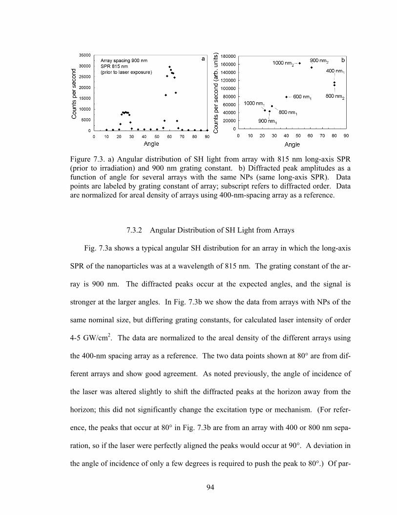
Figure 7.3. a) Angular distribution of SH light from array with 815 nm long-axis SPR (prior to irradiation) and 900 nm grating constant. b) Diffracted peak amplitudes as a function of angle for several arrays with the same NPs (same long-axis SPR). Data points are labeled by grating constant of array; subscript refers to diffracted order. Data are normalized for areal density of arrays using 400-nm-spacing array as a reference.
7.3.2 Angular Distribution of SH Light from Arrays
Fig. 7.3a shows a typical angular SH distribution for an array in which the long-axis
SPR of the nanoparticles was at a wavelength of 815 nm. The grating constant of the ar-
ray is 900 nm. The diffracted peaks occur at the expected angles, and the signal is
stronger at the larger angles. In Fig. 7.3b we show the data from arrays with NPs of the
same nominal size, but differing grating constants, for calculated laser intensity of order
4-5 GW/cm2. The data are normalized to the areal density of the different arrays using
the 400-nm spacing array as a reference. The two data points shown at 80° are from dif-
ferent arrays and show good agreement. As noted previously, the angle of incidence of
the laser was altered slightly to shift the diffracted peaks at the horizon away from the
horizon; this did not significantly change the excitation type or mechanism. (For refer-
ence, the peaks that occur at 80° in Fig. 7.3b are from an array with 400 or 800 nm sepa-
ration, so if the laser were perfectly aligned the peaks would occur at 90°. A deviation in
the angle of incidence of only a few degrees is required to push the peak to 80°.) Of par-
94
ticular interest is the enormous signal strength observed with the photomultiplier tube and
photon counter. For comparison, the maximum signals observed in Ref. [70] were of or-
der 1500 counts/second (cps). Here the maximum signals we present are two orders of
magnitude larger, and in some experiments signals as large as 5 x 10⁵ cps were observed.
To understand this, we must consider the higher incident intensity, the improved resonant
enhancement, and the smaller solid angle subtended by the detector in the present ex-
periment.
7.3.3 Normalization Considerations
A central question re her there is a quadrupole
om
garding the diffraction patterns is whet
c ponent of the intrinsic radiation pattern of the NPs, and its relation to any dipole
component [97]. In certain cases, the quadrupole and dipole contributions can arise from
physically different mechanisms. For instance, in isolated metal nanospheres the quadru-
pole is generated in a local process involving only surface susceptibilities, whereas the
dipole is generated in a nonlocal process involving both surface and volume susceptibili-
ties [96, 101]. In these NPs there is an effective second-order susceptibility tensor com-
ponent of the form )2(||||⊥χ that is nonzero, possibly due to the sole asymmetry in the sys-
tem, that being the differing dielectrics above (air) and below (ITO) the NP. An alterna-
tive mechanism would be a bulk quadrupolar excitation as discussed by Bloembergen et
al. [104], in which the nonlinear polarization in an isotropic centrosymmetric medium
may be written as:
()2( ωP NLv= (7.1) ))()(())()(()())()(2 ωωγωωβωωγβδ EEEEEE
vvvvvvvvv⋅∇+⋅∇+∇⋅−−
95
where the constants γβδ and, contain materials parameters and frequency. In the case
of conducting media the prefactors are as follows:
γβδω
γωπ
β 2,8
,8 42*
30
2* +===m
enme . (7.2)
In Eq. 7.2, is the electronic charge, is the effective electron mass, and is the elec-
tron density of the material. Evidently in the conducting case the first term of Eq. 7.1
vanishes, but Bloembergen cautions that the expression for
e *m 0n
δ “should not be taken too
literally” because of the sensitivity of the term to hydrodynamic forces and surface poten-
tial gradients. γ may also be written as , where )4/( 42 ωωβγ p= pω is the classical
plasma frequency. (Note that CGS units were used in Ref. [104].)
Consider plane wave excitation of the form xtzkiEE x ˆ))ˆ(exp()( 00 ωω −⋅=vv
, where
is the surface normal. If the induced field z )ω(1Ev
inside the particle (mediated by the
particle plasmon) maintains the functional form of the incident light, the first two terms
in Eq. 7.1 vanish and the nonlinear polarization takes the form zti ˆ)2 ωEP x exp()2( 21ω −∝
v,
corresponding to an out-of-plane polarization at the second-harmonic frequency. In this
case the nanoscale optical properties would enter through the transition from 0Ev
to 1Ev
.
To first order, each of these possibilities yields a dipolar SH radiation pattern; how-
ever, due to the large lateral dimensions of the NPs, there could be quadrupolar compo-
nents as well. The selection rule that SHG is forbidden in the forward and backward di-
rections holds for the quadrupole as well as the dipole, so it is only at large observation
angles that they may be distinguished. From a technological perspective, the ability to
manipulate the mechanisms will allow control over the strength and direction(s) of the
96
SH signal. In order to resolve this, it is essential to properly normalize the SH signal at
each diffracted peak. The obvious factors to be normalized are the areal density of parti-
cles in the array and any fluctuations in the incident laser intensity. However, the angular
spread in a given diffracted peak varies drastically with the grating parameters, and must
be accounted for to distinguish dipolar from quadrupolar radiation patterns.
The measured SH angular pattern is the superposition of the multiple-slit diffraction
pattern and the SH radiation pattern, which may be written separately as follows [70, 98]:
2
0
02
sinsinsin)(
∝
αα
ββθ
NN
I diff
(7.3a)
θβθα sin2
,sin2
21 ll kk≡≡ (7.3b,c)
(7.4) θθθθ 222 cossin4sin)( QuadrupoleDipoleSH AAI +∝
Here is the slit spacing, is the slit width, and wavenumber 1l 2l λπ /2=k .
Assuming that the SH radiation pattern is given by a linear combination of dipole and
quadrupole patterns, and are parameters which can be fitted to the data.
The factor of 4 normalizes the maximum of the pure quadrupole pattern to unity, as for
the dipole pattern. The multiple-slit diffraction pattern exhibits the following properties.
As N
DipoleA QuadrupoleA
0 increases, the diffracted peak widths decrease due to improved cancellation, stem-
ming from coherent addition of increasing numbers of Fourier components. As the ratio
of grating spacing to particle size (which is equivalent, by Babinet’s principle, to slit
width) increases, the peak widths decrease. As more and more diffracted orders become
allowed, the allowed orders are increasingly compressed toward the array normal, com-
pressing the peak widths as well. Finally, as the diffracted angle increases, the angular
97
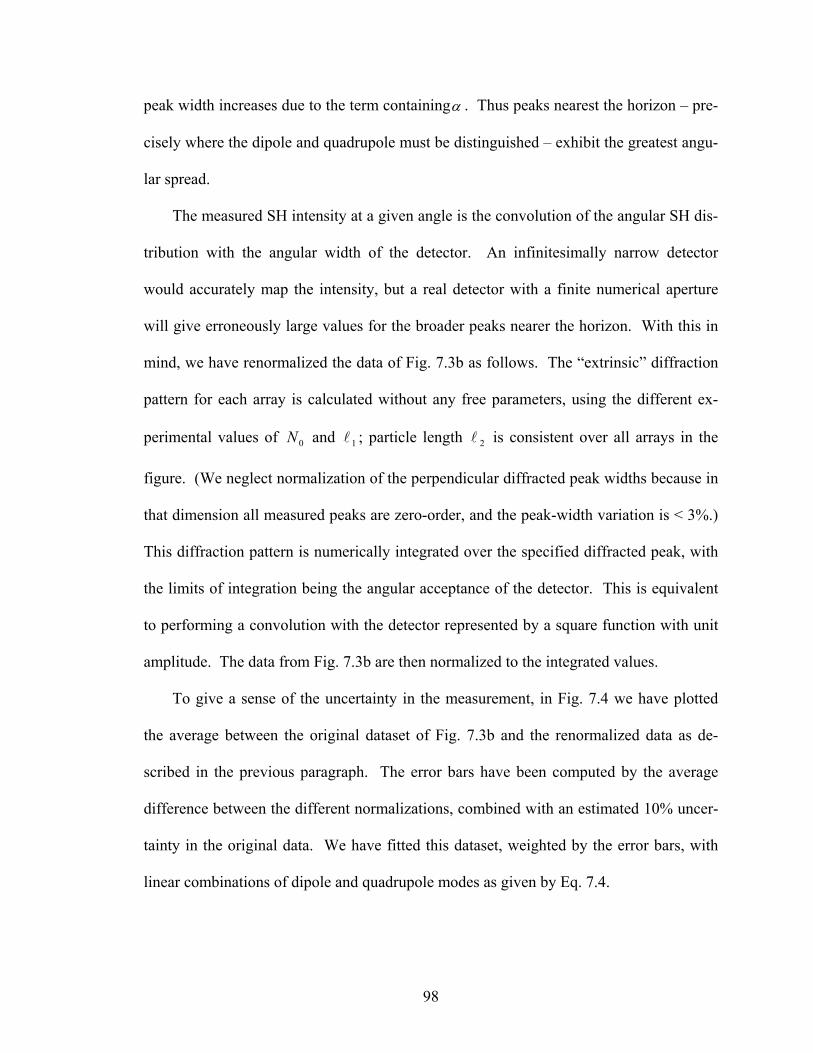
peak width increases due to the term containingα . Thus peaks nearest the horizon – pre-
cisely where the dipole and quadrupole must be distinguished – exhibit the greatest angu-
lar spread.
The measured SH intensity at a given angle is the convolution of the angular SH dis-
tribution with the angular width of the detector. An infinitesimally narrow detector
would accurately map the intensity, but a real detector with a finite numerical aperture
will give erroneously large values for the broader peaks nearer the horizon. With this in
mind, we have renormalized the data of Fig. 7.3b as follows. The “extrinsic” diffraction
pattern for each array is calculated without any free parameters, using the different ex-
perimental values of and ; particle length l is consistent over all arrays in the
figure. (We neglect normalization of the perpendicular diffracted peak widths because in
that dimension all measured peaks are zero-order, and the peak-width variation is < 3%.)
This diffraction pattern is numerically integrated over the specified diffracted peak, with
the limits of integration being the angular acceptance of the detector. This is equivalent
to performing a convolution with the detector represented by a square function with unit
amplitude. The data from Fig. 7.3b are then normalized to the integrated values.
0N 1l 2
To give a sense of the uncertainty in the measurement, in Fig. 7.4 we have plotted
the average between the original dataset of Fig. 7.3b and the renormalized data as de-
scribed in the previous paragraph. The error bars have been computed by the average
difference between the different normalizations, combined with an estimated 10% uncer-
tainty in the original data. We have fitted this dataset, weighted by the error bars, with
linear combinations of dipole and quadrupole modes as given by Eq. 7.4.
98

Figure 7.4. Averaged renormalized data of Fig. 7.3b (see text). Solid line is a fit to Eq. 7.3. Dashed lines are fits (using the same weighting as solid line) to pure dipole and quadrupole patterns respectively.
Clearly, the dataset normalized only for areal density exaggerates the dipole contri-
bution relative to the quadrupole contribution. It appears that the contributions from di-
polar and quadrupolar modes do not differ by orders of magnitude. Further conclusions
based on these data would be premature for three critical reasons. First, the slight align-
ment offset used to make the diffracted peaks appear at 80° introduces greater uncertainty
into those data. Second, the resonant enhancement at the fluence used introduces thermal
effects which change the nanoparticle shape. Third, above a certain threshold the funda-
mental intensity dependence of the SHG changes from 2nd-order to 3rd-order behavior.
The latter effects will now be discussed.
7.3.4 Laser-Induced Morphological Changes in NPs
When the SPR mode of the NPs is tuned to the laser wavelength, laser irradiation
alters NP shape. Figure 7.5 shows scanning electron micrographs of an array before and
after laser exposure. In this case the total exposure time was on the order of one to two
99

Figure 7.5. Scanning electron micrographs of NPs before and after laser irradiation. Im-ages are of the exact same NPs in the same array. Prior to irradiation SPR was 850 nm.
hours; the average power was ~450 mW, implying peak fluence of ~0.23 mJ/cm2. The
original long-axis SPR of the array was 850 nm; however, after irradiation the lateral di-
mensions of the particles are reduced to about half of the former area. Extinction meas-
urements following laser irradiation show that the long-axis resonance has considerably
blueshifted. At the same time, AFM measurements of laser-irradiated particles demon-
strate that the particle heights have approximately doubled relative to the as-deposited
mass thickness. Thus, the particles are being reshaped by the laser beam rather than
shrinking, as in photodesorption; while we have not ruled out all photodesorption, it is
not the dominant effect. Qualitatively, the phenomenon is the “jumping” behavior de-
scribed by Habenicht and coworkers [105], wherein the particles tend to assume a more
spherical shape, increasing the height at the expense of length and width and decreasing
the total surface area of the particle in an attempt to minimize the surface energy. How-
ever, the fluence used here is orders of magnitude less than the fluence used in their ex-
periment (A. Habenicht, personal communication), which is why we do not observe the
range of shapes or the jumping behavior that they found. Our irradiance is much larger
than theirs due to the ultrashort pulse duration, confirming that the fluence is the relevant
parameter.
100
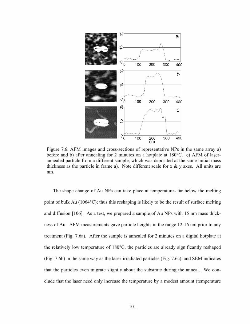
Figure 7.6. AFM images and cross-sections of representative NPs in the same array a) before and b) after annealing for 2 minutes on a hotplate at 180°C. c) AFM of laser-annealed particle from a different sample, which was deposited at the same initial mass thickness as the particle in frame a). Note different scale for x & y axes. All units are nm.
The shape change of Au NPs can take place at temperatures far below the melting
point of bulk Au (1064°C); thus this reshaping is likely to be the result of surface melting
and diffusion [106]. As a test, we prepared a sample of Au NPs with 15 nm mass thick-
ness of Au. AFM measurements gave particle heights in the range 12-16 nm prior to any
treatment (Fig. 7.6a). After the sample is annealed for 2 minutes on a digital hotplate at
the relatively low temperature of 180°C, the particles are already significantly reshaped
(Fig. 7.6b) in the same way as the laser-irradiated particles (Fig. 7.6c), and SEM indicates
that the particles even migrate slightly about the substrate during the anneal. We con-
clude that the laser need only increase the temperature by a modest amount (temperature
101

rise on the order of 100 K) for reshaping to occur. At the 2-minute point, the particles
appear to have reached equilibrium for that temperature; annealing for an additional 2
minutes does not substantially alter the NP shape.
Here we consider a simple model to find the temperature rise in Au NPs. From Fig.
7.2b we note that the extinction efficiency over the laser spectral range in an array with
300 nm spacing is ~0.45, meaning that roughly half the light incident on a 300 x 300 nm2
area (one unit cell) interacts with the particle. Assuming 50-fs pulses and a 50-µm spot
diameter, the peak fluence of the excitation laser is 2.3 x 10⁻⁴ J/cm2. For an Au ellipsoid
with major axes 140 x 110 x 16 nm (which for an effective medium 2=mε has reso-
nance maxima very close to that of Fig. 7.2b), the calculated absorption efficiency ac-
counts for about ¾ of the extinction efficiency; the high absorption is similar to that
found in an equivalent sphere of radius 31 nm. Thus 45% x 75% = 34% of the incident
energy in a 300 x 300 nm2 area is absorbed by the particle, or ~ 7.0 x 10⁻¹⁴ J per pulse. If
we consider the NP to have the bulk molar volume (10.21 cm3/mol) and heat capacity
(~25 J/K/mol) values, the temperature rise due to absorption for a single laser pulse is
approximately 220 K. Still smaller NPs could have larger temperature rises due to lower
volume and increased absorption.
If we consider the effects of pulse repetition frequency as discussed by Gamaly et al.
[107], we find virtually no cumulative temperature buildup at all. In that model, the in-
crease in average sample temperature is given by pppavg ttT /2 max=
ppt
T , where T is the
temperature rise in a single pulse, is pulse duration and is pulse repetition rate. Be-
cause the duty cycle of the laser is small, the cumulative temperature increase over many
pulses is of order 1 K. Nonetheless, the temperature rise due to a single pulse can be
max
pt
102

quite large, and we reiterate that reshaping of the NP takes place at temperatures far be-
low the bulk melting point. The notion that the NPs are reshaped by each individual
pulse, even though there is no cumulative temperature buildup, is supported by the obser-
vation that the laser-irradiated sample does not show the degree of particle migration of
the annealed sample.
Figure 7.7. Intensity dependence of SH signal, with fits to a power law dependence on fundamental intensity. Note log-log scale.
The intensity dependence of the SH signal is shown in Fig. 7.7. The array used in
this measurement had its initial resonance at 770 nm. In these measurements the laser
was only unblocked during the 10 s data acquisition for each point. At an approximate
fluence threshold of ~ 7.3 x 10⁻⁵ mJ/cm2, the power-law exponent fit changes from 2.15
to 3.21. This may indicate that the thermal effects related to the reshaping process fun-
damentally change the nonlinear response of the NPs from 2nd- to 3rd-order. The calcu-
lated temperature rise at the threshold fluence is ~ 70 K. Working just below this level
with arrays whose resonance peak is initially to the red of the excitation laser, we have
still detected reshaping through an increase in SHG. The increase is due to the fact that
103

the reshaping blueshifts the long-axis particle plasmon to be more resonant with the exci-
tation laser. The process takes place on a timescale of a few seconds to minutes.
The error in these measurements is due primarily to the difficulty of aligning the mi-
croscope precisely on the diffracted SH peak; we estimate such errors to be on the order
of 10% of the measured signal. The thermal reshaping and 3rd-order intensity depend-
ence are likely to affect the results of Fig. 7.3b more than experimental error; i.e., there
could be different ratios of dipolar and quadrupolar contributions in the 3rd-order regime
than in the 2nd-order regime.
7.4 Conclusions
We have observed SHG from arrays of resonantly excited Au nanoparticles. The
unique angular detection capability of our apparatus permits us to compare the relative
magnitudes of dipolar and quadrupolar radiation patterns experimentally, once thermal
effects such as reshaping have been properly accounted for. The SHG mechanism and
the phase-matching condition enforced by the grating set this method apart from hyper-
Rayleigh scattering (HRS) measurements [16, 74, 97], which measure an incoherent sig-
nal.
The directionality provided by the grating could have applications in nonlinear opti-
cal signal generation and routing. An array excited at normal incidence whose grating
constant is an integer multiple of the SH wavelength will have a strong diffracted peak
running along the surface of the sample. This property could be used to excite fluores-
cent molecules in the plane of, but some distance away from, the NP array. It could also
be exploited in waveguide geometries. The SHG mechanism in concert with the grating
104

effect could also be a useful probe of fluorescent molecules adsorbed directly on the NPs
with specific orientations.
The strong interaction between the light and the NPs makes thermal reshaping ef-
fects important. One way to preserve the original dimensions of the NPs might be to cap
the NP array with some material as a physical barrier. A capping layer could be useful in
other ways: capping the array with ITO, for instance, would remove the asymmetry in the
dielectric environment, in which case the HRS mechanisms proposed by Dadap et al. [96,
101] would become dominant. Such a method could be used to probe those HRS mecha-
nisms directly and compare the SH strength and radiation pattern with these results. The
other important effect of a capping layer is to change the spectral location of the SPR; the
particle shape and size would need to be altered in order to maintain the resonant en-
hancement with the excitation laser. The reshaping is an interesting phenomenon in it-
self, as it likely relates to the surface tension generated by the small size and large curva-
ture of the NPs [106, 108]; the process dynamics could be studied in an ultrafast pump-
probe geometry with a broadband continuum probe pulse.
105
CHAPTER VIII
REDUCED SECOND HARMONIC GENERATION FROM CLOSELY SPACED PAIRS OF Au NANOPARTICLES
Closely spaced pairs or “dimers” of elongated gold nanoparticles may be expected to
exhibit electric field hotspots. We investigate the possible influence of hotspots on sec-
ond harmonic generation. Preliminary results show that arrays of nanoparticle dimers
exhibit reduced second-harmonic generation compared with arrays of single nanoparti-
cles having similar extinction spectra, contradicting a simple model of second-harmonic
generation (varying as the fourth power of the local fundamental field).§§
8.1 Introduction
The linear optical properties of MNPs have been known for nearly a century and
have been widely examined through experiment over the past several decades [2, 3, 33].
The nonlinear optical properties are not nearly as well-characterized, as even the theory
of second-harmonic generation from small spheres in homogeneous media was not pub-
lished until relatively recently [96, 101]. Most studies of SHG from lithographic arrays
of NPs have focused on its utility as a tool for autocorrelation measurements of plasmon
dephasing, which are unworkable in conventional measurement geometries for particles
with in-plane inversion symmetry [81, 83]. The simplest model of SHG in MNPs is that
the SH intensity is proportional to the fourth power of the local fundamental electric field
(that is, the SH intensity goes as the square of the fundamental intensity). It is well-
known that in nanoscale metals, particularly at sharp edges or in small gaps, local “hot §§ The content of this chapter has been accepted for publication in Proceedings of the SPIE.
106
spots” of greatly increased electric field can occur [86, 109]. These are thought to be re-
lated to the unpredictability of surface-enhanced Raman scattering measurements, for ex-
ample, and control of such hot spots is a major goal of nanoscale photonics. This raises
the question of whether hot spots can be exploited to enhance SHG from a spatially con-
trolled metal nanoparticle system.
We have shown that it is possible to measure SH at non-normal observation angles
from MNPs with planar symmetry arranged in diffraction gratings; the angular distribu-
tion of SH light is the superposition of the radiation pattern of an individual particle with
the overall grating pattern [70]. Here, we use this phenomenon to study the effects of
particle arrangements on SHG, using “dimer” structures consisting of closely spaced Au
nanoparticles that might be expected to exhibit local field enhancements [86]. The ex-
tinction characteristics of similar structures have been studied in some detail. Rechberger
and coworkers [36] studied pairs of Au disks and found good agreement with a simple
dipole-pair model; strong interactions were found for interparticle distances of 50 nm or
less. Gunnarsson and coworkers [37] studied isolated pairs of Ag disks and found strong
interparticle interactions when the separation was less than ~30 nm. However, no SHG
studies of organized dimer structures have been published. SHG from arrays of asym-
metric MNPs has been studied, but primarily with attention to dephasing. Another recent
study of SHG from MNPs examined Ag nano-pyramids in a hexagonal lattice; no dra-
matic enhancement effects were observed, and this was attributed to the sample symme-
try [110]. Studies of SHG from nano-rough metal surfaces indicated the presence of
nanoscale SH hotspots, but relied on random surface features to generate SH [99]. In this
study, we report the unexpected finding that dimers exhibit reduced SHG compared with
107
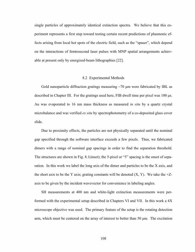
single particles of approximately identical extinction spectra. We believe that this ex-
periment represents a first step toward testing certain recent predictions of plasmonic ef-
fects arising from local hot spots of the electric field, such as the “spaser”, which depend
on the interactions of femtosecond laser pulses with MNP spatial arrangements achiev-
able at present only by energized-beam lithographies [22].
8.2 Experimental Methods
Gold nanoparticle diffraction gratings measuring ~70 µm were fabricated by IBL as
described in Chapter III. For the gratings used here, FIB dwell time per pixel was 100 µs.
Au was evaporated to 16 nm mass thickness as measured in situ by a quartz crystal
microbalance and was verified ex situ by spectrophotometry of a co-deposited glass cover
slide.
Due to proximity effects, the particles are not physically separated until the nominal
gap specified through the software interface exceeds a few pixels. Thus, we fabricated
dimers with a range of nominal gap spacings in order to find the separation threshold.
The structures are shown in Fig. 8.1(inset); the 5-pixel or “5” spacing is the onset of sepa-
ration. In this work we label the long axis of the dimer and particles to be the X axis, and
the short axis to be the Y axis; grating constants will be denoted (X, Y). We take the +Z-
axis to be given by the incident wavevector for convenience in labeling angles.
SH measurements at 400 nm and white-light extinction measurements were per-
formed with the experimental setup described in Chapters VI and VII. In this work a 4X
microscope objective was used. The primary feature of the setup is the rotating detection
arm, which must be centered on the array of interest to better than 50 µm. The excitation
108
laser was a Ti:Sapphire (KMLabs) producing 50-fs pulses centered at 805 nm, entering at
normal incidence from the rear of the sample. To ensure that we worked in the second-
order intensity regime, we used relatively low laser power (~100 mW). For intentional
reshaping we used the maximum output power 345 mW, with the focusing lens slightly
defocused in order to illuminate the array more homogeneously. AFM indicates that
even at 100 mW, some reshaping takes place; we attempted to do the SH measurements
with as little laser exposure as possible.
As the physical gap opens up in the dimer, there is a fundamental change in the grat-
ing structure along the dimer. The presence of a nearby particle alters the phase of the
constructive interference compared with the single-particle case. When the dimer gap
approaches one-half the grating constant, the grating spacing is effectively halved. In
less extreme cases the opening of the gap primarily reduces the amplitude of the original
diffracted peak. To circumvent this complication, we can measure the diffracted SH in
the YZ-plane, perpendicular to the dimer long axis. The YZ configuration has the addi-
tional advantage that a quadrupole mode will not radiate in the YZ-plane, so the radiation
will be dipolar [96]; for single particles, comparison of XZ and YZ results should allow
separation of dipolar and quadrupolar effects. Since we cannot easily modify our detec-
tor rotation plane, we rotated both the physical sample and the laser polarization using a
λ/2 plate to measure in the YZ-plane (Fig 8.2, inset).
109
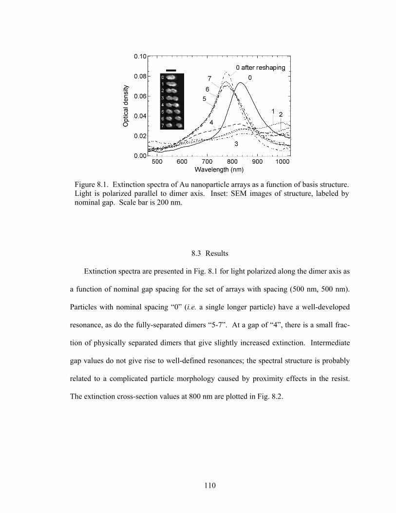
Figure 8.1. Extinction spectra of Au nanoparticle arrays as a function of basis structure.Light is polarized parallel to dimer axis. Inset: SEM images of structure, labeled by nominal gap. Scale bar is 200 nm.
8.3 Results
Extinction spectra are presented in Fig. 8.1 for light polarized along the dimer axis as
a function of nominal gap spacing for the set of arrays with spacing (500 nm, 500 nm).
Particles with nominal spacing “0” (i.e. a single longer particle) have a well-developed
resonance, as do the fully-separated dimers “5-7”. At a gap of “4”, there is a small frac-
tion of physically separated dimers that give slightly increased extinction. Intermediate
gap values do not give rise to well-defined resonances; the spectral structure is probably
related to a complicated particle morphology caused by proximity effects in the resist.
The extinction cross-section values at 800 nm are plotted in Fig. 8.2.
110

Figure 8.2. Extinction at 800 nm (left axis) and second harmonic intensity (right axis; note log scale) as a function of basis structure. RS = reshaping. Inset: schematic of measurement geometry, where detector angle is varied in YZ-plane.
Diffracted SH intensities are also plotted in Fig. 8.2 (note log scale for right axis).
All data points are taken at the same diffracted angle, so we need not normalize for the
extrinsic diffraction pattern as we did for the measurement in Chapter VII. In general,
the SH output follows the extinction cross-section, regardless of whether there is a well-
developed resonance. However, there is an important exception. The “0” array (consist-
ing of single particles with well-developed resonance) gives nearly twice as much SH
output as the “5-7” dimer arrays even though the “0” extinction at 800 nm is somewhat
less. Since the laser spectrum matched the “0” array extinction better than that of the
others, perhaps this could be explained by some effect, thermal or otherwise, that would
violate the superposition principle. To explicitly rule this out, we reshaped the “0” array
to shift the extinction spectra to better match the dimer arrays. Reshaping was achieved
by illuminating with a slightly defocused full-power laser beam for 2 minutes, resulting
111
in an extinction peak that more closely matches the “5-7” dimers (Fig. 8.1). The narrow-
ing and strength increase are partially attributed to increased homogeneity. We measured
SH from the reshaped array and found a slight increase in the SH output, as shown in Fig.
8.2 (empty data points). This demonstrates that the extinction at 800 nm is the relevant
parameter, rather than the resonance with the laser spectrum at other wavelengths.
8.4 Discussion
The simplest geometric approximation to these particle shapes is the general ellip-
soid (semiaxes a ). Calculations of the LSPR modes for general ellipsoids [4] sat-
isfying an arbitrary “flatness” condition show that the out-of-plane LSPR
mode is unchanged (within 2 nm) over a large range of a and b values and generally oc-
curs at the shortest wavelength that the dielectric function allows. By contrast, the in-
plane spectral positions may vary by hundreds of nm over the same range. Thus we ex-
pect that the out-of-plane mode is virtually constant for all particles studied. In addition,
the fact that the SH does not seem to change much with increasing dimer gap suggests
that near-field coupling of the out-of-plane modes is relatively weak.
cb ≥≥
cba 2>≥
In previous work we used a simple model of SHG in which the SH intensity varies as
the fourth power of the local fundamental field (LFF) [70]. The LFF is given by the su-
perposition of the incident field with the polarization induced in the NP, so for the SH
intensity
4)1( αεv
LI mdSH −∝ . (8.1)
dL is a depolarization factor (as in Ref. [4] p. 147), mε the dielectric function of the em-
bedding medium, the NP volume and v α its polarizability. (Here we have assumed that
112

the direction is that of laser polarization.) In this model, the extinction cross-section is
related to SHG indirectly through the particle polarizability. For flat ellipsoids similar to
our NPs, calculations show that scattering and absorption are comparable at 800
nm k/2π= . Since polarizability is directly proportional to volume, volume cancels from
the SH expression but not from the extinction cross-section. As the long axis of an NP is
reduced, the cross-section for the long-axis mode blueshifts and weakens. The SHG pre-
dicted by this model blueshifts as well, but the amplitude is more complicated, reflecting
an intricate interplay between the polarizability and the depolarization (which depends on
geometry and dielectric behavior). To illustrate this we have calculated extinction cross-
sections and SH response from two different ellipsoids using the MLWA (see Section
2.5), designed to have extinction maxima on opposite sides of 800 nm but identical ex-
tinction cross-section at 800 nm. In a variety of cases studied, we find that the shorter-
wavelength NP always gives more SHG than a longer-wavelength NP for equivalent ex-
tinction at 800 nm. This is a property of the metallic dielectric function of Au in the 800-
nm region [40]; if we input a fictitious dielectric function with similar real values but op-
posite slope, the behavior is reversed.
This model is contradicted by our results. The dimer particles (“5-7”) are smaller
and their resonance maxima shorter than 800 nm, yet even in spite of the small interparti-
cle gaps (which are not included in the simple model above) they exhibit considerably
less SH output than the larger, redder “0” particles. We point out that we do not observe
clear evidence (spectral shifts) of strong interparticle interactions in the extinction spec-
tra. This is probably due to inhomogeneities in our sample. Strong spectral shifts rela-
113

tive to isolated disks have been observed in pairs of Ag disks with similar separation; the
shifts are highly sensitive to small differences in the gap distance [37].
It is not clear from these results what the effects of local electric field hotspots on
SHG would be. Since there is not much variation in the linear spectra with gap separa-
tions up to a particle length, the smallest gap sizes here may yet be too large to elicit
strong hotspots. This hypothesis can be tested experimentally through more-
homogeneous samples, and computationally through more-detailed calculations based on
a discrete dipole approximation or a finite-difference-time-domain method. On the other
hand, if hotspots do in fact exist in these gaps, then it would appear that hotspots do not
enhance SHG, but rather divert energy into other channels, such as non-radiative excita-
tions.
114

CHAPTER IX
SUMMARY
The goal of this dissertation has been to explore the linear and nonlinear optical
properties of lithographically-prepared ordered arrays of metal nanoparticles. In particu-
lar we have examined the effects of diffractive behavior caused by the array periodicity.
We showed in Chapter IV through optical and Auger spectroscopy that silver
nanoparticles tarnish more readily than bulk Ag in air. This result highlights both the in-
creased chemical reactivity in nanoscale particles and the high sensitivity of the LSPR to
small changes in the local dielectric surroundings. It also presents a caution regarding the
interpretation of optical spectra from silver nanoparticles exposed to ambient. In Chapter
V we demonstrated diffraction from metal nanoparticle arrays in a frustrated-total-
internal-reflection measurement, showing that the diffraction is fairly robust even when
the particles are largely destroyed.
The diffractive character of ordered arrays may be exploited to study second-
harmonic generation from metal nanoparticles, which we explored in Chapters VI-VIII.
The non-normal angles of the diffracted peaks allow us to examine particles possessing
in-plane symmetry, in contrast to normal-incidence geometries. When the particle plas-
mon is tuned to match the excitation wavelength, the second-harmonic signal is reso-
nantly enhanced to levels that are particularly striking when the source volume is consid-
ered. There is anecdotal evidence suggesting that for high incident fluence the second-
harmonic light from MNP arrays may be visible to the unaided eye. These resonant opti-
115

cal effects are partially obscured by thermal effects, such as surface melting, that occur at
high excitation fluence.
Using the diffraction as a heuristic for studying second-order nonlinearities, we have
begun to examine the effects of local field enhancements on second-harmonic generation.
The first results suggest the possibility that near-field interactions between neighboring
particles may suppress SHG relative to single nanoparticles. Further tests are necessary
to confirm or confute this idea.
There are many possibilities for future study with diffracted harmonic light. I now
present a brief list of experiments which seem to be natural extensions of the work pre-
sented in this dissertation.
• The question of dipole vs. quadrupole SH radiation modes, raised in Chapters VI
and VII, has not been definitively answered. Careful measurements with arrays
whose grating constant is finely controlled are needed to probe the near-horizon dif-
fracted angles. The rather minor technical difficulty is that near the horizon, the an-
gle depends most strongly on the grating spacing, so fine control of grating spacing
is needed to specify the angle.
• For arrays whose grating constant exactly matches the second-harmonic wavelength,
the SH light should be radiated directly across the sample plane. The propagation of
SH light across the sample could be probed with fluorescent markers to find propa-
gation lengths. SH light could also conceivably be produced in a waveguide geome-
try for similar effect.
• An important question regarding resonantly enhanced SH light is the strength of the
resonant enhancement and the character of the excitation in the absence of any ther-
116
mal reshaping. Since second-harmonic intensity should depend on the incident in-
tensity, not fluence, it will be beneficial to reduce the pulse duration of the laser as
much as possible. If a 12-fs pulse can be achieved (most recently the shortest pulse
achieved is ~20 fs; the bandwidth of the laser is sufficient to produce 12-fs pulses),
the second-harmonic intensity could be increased by a factor of ~16, allowing a dra-
matic decrease in fluence which should reduce and eventually eliminate thermal ef-
fects.
• It would be of particular interest to measure the pulse duration of the diffracted sec-
ond-harmonic light. The grating provides transverse phase-matching, but the coher-
ence properties of the second-harmonic light are yet unknown.
• There are well-known polarization selection rules for SHG (see Refs. [21, 75, 97,
100]) analogous to the dipole/quadrupole selection rules mentioned in the disserta-
tion. These could be studied in the present experimental apparatus by inserting ro-
tating polarizers at appropriate places in the optical path.
• The computations presented in Chapter II can be enhanced by the introduction of
more precise numerical methods for arbitrary particle shapes. The Discrete Dipole
Approximation is similar in spirit to the CDA and exists for such a purpose. In ad-
dition, it may be feasible to model the effects of a substrate near a metal nanoparti-
cle rather than using an effective-medium approach [7]. If the second-order nonlin-
earities can be connected to the LSPR in a straightforward manner, it may be inter-
esting to study a kind of nonlinear coupled-dipole model including the second-order
behavior. Already, quadrupolar components can be inserted into the CDA without
117

too much pain [33]; so if the SH turns out to be primarily quadrupolar this should
not present insurmountable difficulty.
In summary, this work has unlocked a door to a potential wealth of information
about the nonlinear (second-order, in particular) optical properties of metal nanoparticles.
This information is made available by exploiting the phase-matching provided by the
grating, which results from the ordered arrangement of the nanoparticles.
118

APPENDIX
COMPUTER PROGRAMS
For the interested programmer, I have appended several sample MATLAB files used
in the CDA computations. For convenience, to avoid lengthening the List of Figures un-
necessarily I have labeled each file as a separate Figure, but these Figures can extend
over several pages.
Figure A.1 is a CDA program for oblate ellipsoids. Figure A.2 is the driver file to
call the program of Fig. A.1. Figure A.3 is a CDA program for spheres, including the
quasistatic, MLWA and Mie-dipole versions of the sphere polarizability, from which I
have stripped the majority of the array-creation and file-handling code.
Figure A.4 is the integrand function, which is called by the CDA programs to calcu-
late the detector response, and itself calls two custom functions. Figure A.5 is the func-
tion “mcross4.m”, which is a custom generalized version of the built-in MATLAB matrix
cross-product function “mcross.m”. Figure A.6 is a similar custom cross-product func-
tion which I have named “arraycross.m”. Each of these functions takes two matrices of
3-vectors as inputs. MCross4 computes the cross-products of each 3-vector in matrix A
with each 3-vector in matrix B. ArrayCross requires that A and B have the same dimen-
sion, and only computes the cross-products of 3-vectors having the same column index in
A and B; the result of ArrayCross is a matrix with the same dimensions as A and B.
Computation efficiency can be improved by writing custom function files like these for
each combination of the desired dimensions of the input vectors or matrices.
119

Figure A.1.1. CDA program for oblate ellipsoids, page 1 of 5.
120

Figure A.1.2. CDA program for oblate ellipsoids, page 2 of 5.
121
122
Figure A.1.3. CDA program for oblate ellipsoids, page 3 of 5
Figure A.1.4. CDA program for oblate ellipsoids, page 4 of 5
123
Figure A.1.5. CDA program for oblate ellipsoids, page 5 of 5
124

Figure A.2. Driver program to call the function “CDAprogramE,m” defined in Fig. A.1.
125
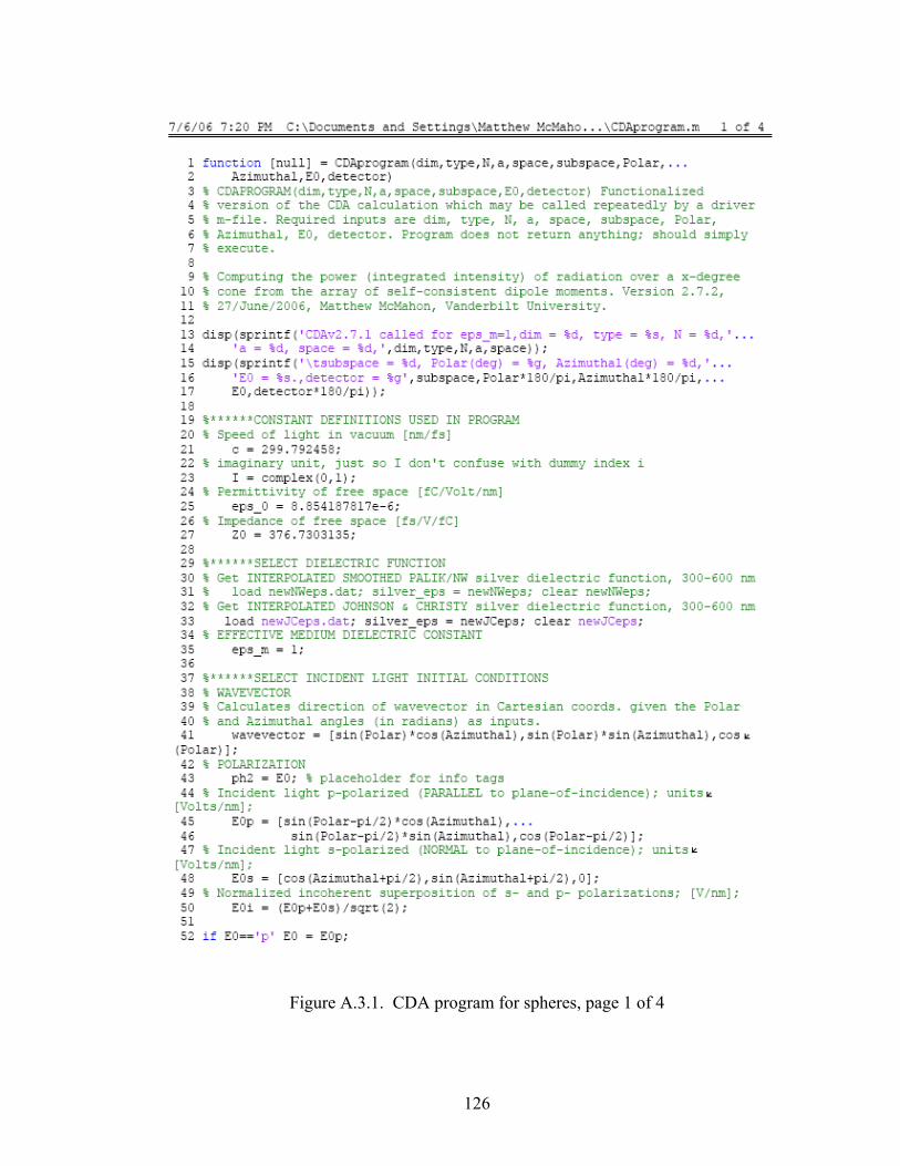
126
Figure A.3.1. CDA program for spheres, page 1 of 4
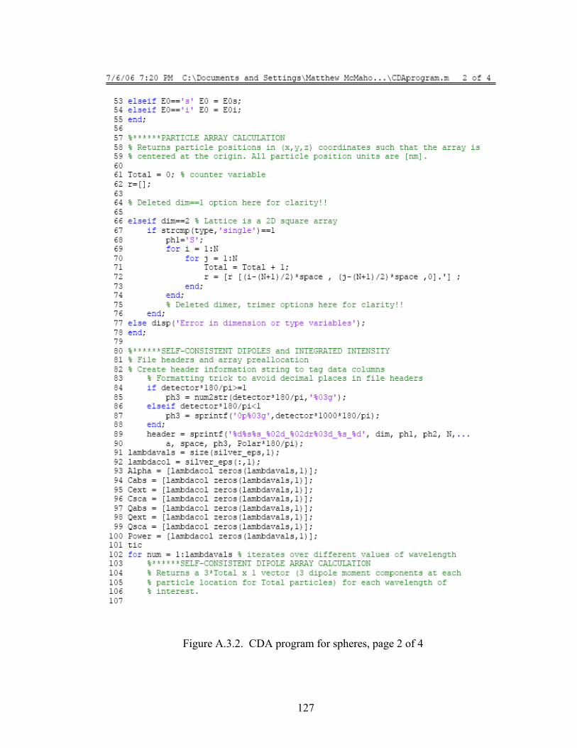
Figure A.3.2. CDA program for spheres, page 2 of 4
127
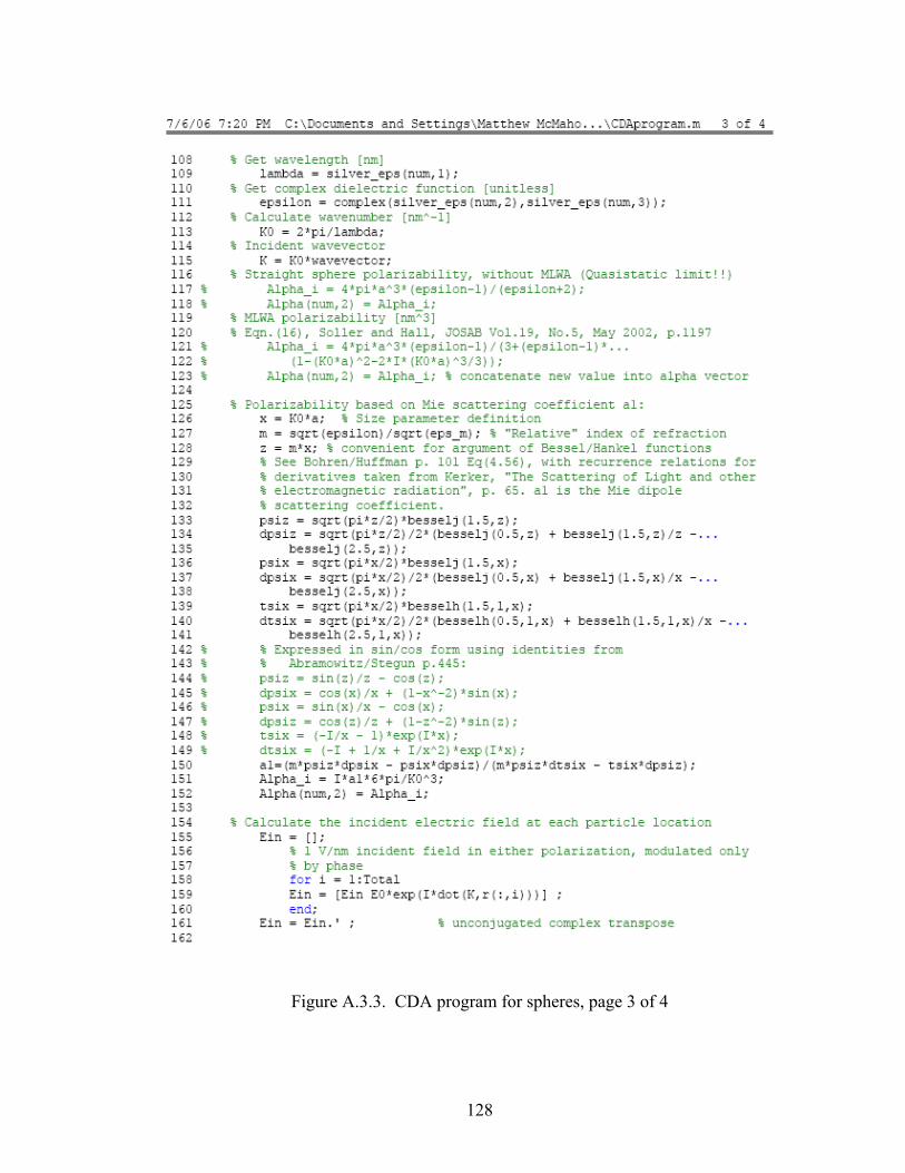
Figure A.3.3. CDA program for spheres, page 3 of 4
128
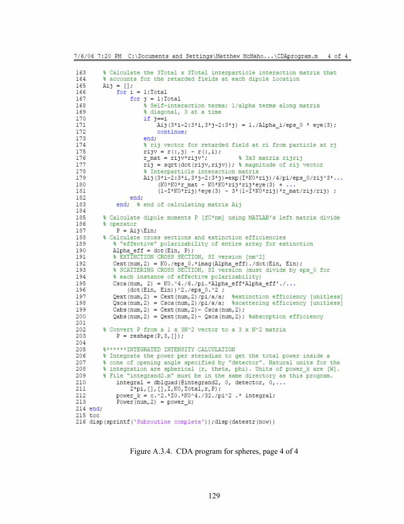
129
Figure A.3.4. CDA program for spheres, page 4 of 4
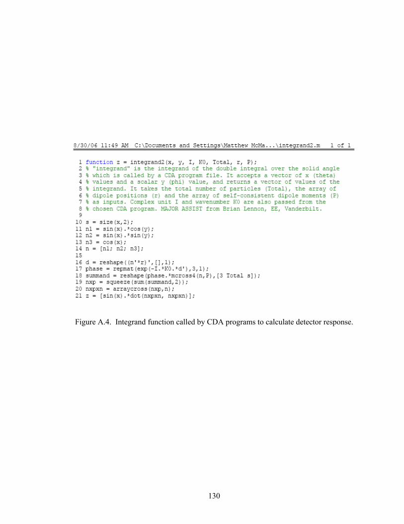
Figure A.4. Integrand function called by CDA programs to calculate detector response.
130
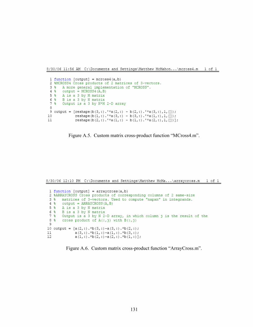
Figure A.5. Custom matrix cross-product function “MCross4.m”.
Figure A.6. Custom matrix cross-product function “ArrayCross.m”.
131

REFERENCES
[1] M. Faraday, Philosophical Transactions of the Royal Society of London, Series A 147, 145 (1857).
[2] G. Mie, Annalen der Physik 25, 377 (1908).
[3] U. Kreibig and M. Vollmer, Optical Properties of Metal Clusters. Springer Series in Materials Science, Vol. 25, Springer Verlag, Berlin-Heidelberg, 1995.
[4] C. F. Bohren and D. R. Huffman, Absorption and Scattering of Light by Small Parti-cles. Wiley-Interscience, New York, 1983.
[5] H. Raether, Surface Plasmons. Springer-Verlag, Berlin, 1988.
[6] N. W. Ashcroft and N. D. Mermin, Solid State Physics. Holt, Rinehart and Winston, Philadelphia, 1976.
[7] B. J. Soller and D. G. Hall, Journal of the Optical Society of America B 19, 1195 (2002).
[8] W. Gotschy, K. Vonmetz, A. Leitner, and F. R. Aussenegg, Applied Physics B 63, 381 (1996).
[9] A. J. Haes and R. P. Van Duyne, Journal of the American Chemical Society 124, 10596 (2002).
[10] A. J. Haes, S. L. Zou, G. C. Schatz, and R. P. Van Duyne, Journal of Physical Chemistry B 108, 6961 (2004).
[11] A. J. Haes, S. L. Zou, G. C. Schatz, and R. P. Van Duyne, Journal of Physical Chemistry B 108, 109 (2004).
[12] A. D. McFarland and R. P. Van Duyne, Nano Letters 3, 1057 (2003).
[13] H. G. Craighead and G. A. Niklasson, Applied Physics Letters 44, 1134 (1984).
[14] B. Lamprecht, G. Schider, R. T. Lechner, H. Ditlbacher, J. R. Krenn, A. Leitner, and F. R. Aussenegg, Physical Review Letters 84, 4721 (2000).
[15] A. Christ, S. G. Tikhodeev, N. A. Gippius, J. Kuhl, and H. Giessen, Physical Re-view Letters 91, 183901 (2003).
[16] R. C. Johnson, J. T. Li, J. T. Hupp, and G. C. Schatz, Chemical Physics Letters 356, 534 (2002).
[17] A. Wokaun, J. G. Bergman, J. P. Heritage, A. M. Glass, P. F. Liao, and D. H. Olson, Physical Review B 24, 849 (1981).
132
133
[18] N. I. Zheludev and V. I. Emel'yanov, Journal of Optics A 6, 26 (2004).
[19] Y. Cui, M. T. Bjork, J. A. Liddle, C. Sonnichsen, B. Boussert, and A. P. Alivisatos, Nano Letters 4, 1093 (2004).
[20] A. J. Haes, C. L. Haynes, A. D. McFarland, G. C. Schatz, R. R. Van Duyne, and S. L. Zou, MRS Bulletin 30, 368 (2005).
[21] B. K. Canfield, S. Kujala, K. Jefimovs, Y. Svirko, J. Turunen, and M. Kauranen, Journal of Optics A 8, S278 (2006).
[22] D. J. Bergman and M. I. Stockman, Physical Review Letters 90, 027402 (2003).
[23] S. A. Maier, M. L. Brongersma, P. G. Kik, S. Meltzer, A. A. G. Requicha, and H. A. Atwater, Advanced Materials 13, 1501 (2001).
[24] S. A. Maier and H. A. Atwater, Journal of Applied Physics 98, (2005).
[25] H. M. Gibbs, Optical bistability: controlling light with light. Academic Press, Or-lando, 1985.
[26] R. Fuchs, Physical Review B 11, 1732 (1975).
[27] S. Asano and G. Yamamoto, Applied Optics 14, 29 (1975).
[28] M. I. Mishchenko, L. D. Travis, and D. W. Mackowski, Journal of Quantitative Spectroscopy & Radiative Transfer 55, 535 (1996).
[29] S. A. Maier, P. G. Kik, and H. A. Atwater, Physical Review B 67, (2003).
[30] T. Jensen, L. Kelly, A. Lazarides, and G. C. Schatz, Journal of Cluster Science 10, 295 (1999).
[31] E. Moreno, D. Erni, C. Hafner, and R. Vahldieck, Journal of the Optical Society of America A 19, 101 (2002).
[32] A. A. Lazarides and G. C. Schatz, Journal of Chemical Physics 112, 2987 (2000).
[33] K. L. Kelly, E. Coronado, L. L. Zhao, and G. C. Schatz, Journal of Physical Chem-istry B 107, 668 (2003).
[34] J. D. Jackson, Classical Electrodynamics. 3rd ed., John Wiley & Sons, Inc., New York, 1999.
[35] L. L. Zhao, K. L. Kelly, and G. C. Schatz, Journal of Physical Chemistry B 107, 7343 (2003).
[36] W. Rechberger, A. Hohenau, A. Leitner, J. R. Krenn, B. Lamprecht, and F. R. Aussenegg, Optics Communications 220, 137 (2003).

134
[37] L. Gunnarsson, T. Rindzevicius, J. Prikulis, B. Kasemo, M. Kall, S. L. Zou, and G. C. Schatz, Journal of Physical Chemistry B 109, 1079 (2005).
[38] S. L. Zou, N. Janel, and G. C. Schatz, Journal of Chemical Physics 120, 10871 (2004).
[39] Handbook of Optical Constants of Solids. ed. E.D. Palik, Academic Press, 1985.
[40] P. B. Johnson and R. W. Christy, Physical Review B 6, 4370 (1972).
[41] M. Quinten and U. Kreibig, Applied Optics 32, 6173 (1993).
[42] M. Moskovits, I. Srnova-Sloufova, and B. Vlckova, Journal of Chemical Physics 116, 10435 (2002).
[43] W. T. Doyle, Physical Review B 39, 9852 (1989).
[44] M. Abramowitz and I. A. Stegun, Handbook of mathematical functions with formu-las, graphs and mathematical tables. 10th ed., National Bureau of Standards Ap-plied Mathematics Series, Vol. 55, U. S. Department of Commerce, Washington, D.C., 1972.
[45] N. V. Voshchinnikov and V. G. Farafonov, Astrophysics and Space Science 204, 19 (1993).
[46] N. W. Liu, A. Datta, C. Y. Liu, and Y. L. Wang, Applied Physics Letters 82, 1281 (2003).
[47] H. G. Craighead, Journal of Applied Physics 55, 4430 (1984).
[48] R. Lopez, L. C. Feldman, and R. F. Haglund, Physical Review Letters 93, 177403 (2004).
[49] M. D. McMahon, R. Lopez, H. M. Meyer, L. C. Feldman, and R. F. Haglund, Ap-plied Physics B 80, 915 (2005).
[50] A. Yelon, K. N. Piyakis, and E. Sacher, Surface Science 569, 47 (2004).
[51] A. Pinchuk, U. Kreibig, and A. Hilger, Surface Science 557, 269 (2004).
[52] U. Kreibig, G. Bour, A. Hilger, and M. Gartz, Physica Status Solidi A 175, 351 (1999).
[53] J. M. Bennett, J. L. Stanford, and E. J. Ashley, Journal of the Optical Society of America 60, 224 (1970).
[54] J. L. Stanford, Journal of the Optical Society of America 60, 49 (1970).
135
[55] B. T. Reagor and J. D. Sinclair, Journal of the Electrochemical Society 128, 701 (1981).
[56] J. P. Franey, G. W. Kammlott, and T. E. Graedel, Corrosion Science 25, 133 (1985).
[57] T. E. Graedel, J. P. Franey, G. J. Gaultieri, G. W. Kammlott, and D. L. Malm, Cor-rosion Science 25, 1163 (1985).
[58] T. Brandt, W. Hoheisel, A. Iline, F. Stietz, and F. Träger, Applied Physics B 65, 793 (1997).
[59] U. Kreibig, M. Gartz, and A. Hilger, Berichte der Bunsen-Gesellschaft fuer Physi-kalische Chemie 101, 1593 (1997).
[60] J. H. Payer, G. Ball, B. I. Rickett, and H. S. Kim, Materials Science & Engineering A A198, 91 (1995).
[61] Handbook of Chemistry and Physics. CRC Press, Boca Raton, FL, 2003-2004.
[62] D. K. Burge, J. M. Bennett, R. L. Peck, and H. E. Bennett, Surface Science 16, 303 (1969).
[63] S. A. Maier, M. L. Brongersma, P. G. Kik, and H. A. Atwater, Physical Review B 65, 193408 (2002).
[64] S. A. Maier, P. G. Kik, and H. A. Atwater, Applied Physics Letters 81, 1714 (2002).
[65] S. A. Maier, P. G. Kik, H. A. Atwater, S. Meltzer, E. Harel, B. E. Koel, and A. A. G. Requicha, Nature Materials 2, 229 (2003).
[66] N. Felidj, et al., Physical Review B 65, 075419 (2002).
[67] C. L. Haynes, et al., Journal of Physical Chemistry B 107, 7337 (2003).
[68] S. Linden, J. Kuhl, and H. Giessen, Physical Review Letters 86, 4688 (2001).
[69] C. Sonnichsen, et al., Applied Physics Letters 77, 2949 (2000).
[70] M. D. McMahon, R. Lopez, R. F. Haglund, E. A. Ray, and P. H. Bunton, Physical Review B 73, 041401 (2006).
[71] T. Götz, M. Buck, C. Dressler, F. Eisert, and F. Träger, Applied Physics A 60, 607 (1995).
[72] F. R. Aussenegg, A. Leitner, and H. Gold, Applied Physics A 60, 97 (1995).
[73] B. Lamprecht, A. Leitner, and F. R. Aussenegg, Applied Physics B 64, 269 (1997).
136
[74] E. C. Hao, G. C. Schatz, R. C. Johnson, and J. T. Hupp, Journal of Chemical Phys-ics 117, 5963 (2002).
[75] B. K. Canfield, S. Kujalal, K. Jefimovs, T. Vallius, J. Turunen, and M. Kauranen, Journal of Optics A 7, S110 (2005).
[76] A. M. Malvezzi, M. Patrini, A. Stella, P. Tognini, P. Cheyssac, and R. Kofman, European Physical Journal D 16, 321 (2001).
[77] A. Podlipensky, J. Lange, G. Seifert, H. Graener, and I. Cravetchi, Optics Letters 28, 716 (2003).
[78] Y. R. Shen, The Principles of Nonlinear Optics. John Wiley and Sons, New York, 1984.
[79] T. Vartanyan, M. Simon, and F. Trager, Applied Physics B 68, 425 (1999).
[80] M. Simon, F. Trager, A. Assion, B. Lang, S. Voll, and G. Gerber, Chemical Physics Letters 296, 579 (1998).
[81] B. Lamprecht, A. Leitner, and F. R. Aussenegg, Applied Physics B 68, 419 (1999).
[82] B. Lamprecht, J. R. Krenn, A. Leitner, and F. R. Aussenegg, Applied Physics B 69, 223 (1999).
[83] B. Lamprecht, J. R. Krenn, A. Leitner, and F. R. Aussenegg, Physical Review Let-ters 83, 4421 (1999).
[84] H. G. Bingler, H. Brunner, A. Leitner, F. R. Aussenegg, and A. Wokaun, Molecular Physics 85, 587 (1995).
[85] P. F. Liao, J. G. Bergman, D. S. Chemla, A. Wokaun, J. Melngailis, A. M. Hawry-luk, and N. P. Economou, Chemical Physics Letters 82, 355 (1981).
[86] E. Hao and G. C. Schatz, Journal of Chemical Physics 120, 357 (2004).
[87] R. F. Haglund, L. Yang, R. H. Magruder, J. E. Wittig, K. Becker, and R. A. Zuhr, Optics Letters 18, 373 (1993).
[88] G. Assanto, G. Stegeman, M. Sheikbahae, and E. Vanstryland, Applied Physics Let-ters 62, 1323 (1993).
[89] Y. Chiu, U. Rambabu, M. H. Hsu, H. P. D. Shieh, C. Y. Chen, and H. H. Lin, Jour-nal of Applied Physics 94, 1996 (2003).
[90] T. F. Heinz, Second-order nonlinear optical effects at surfaces and interfaces, in Nonlinear Surface Electromagnetic Phenomena, H.-E. Ponath and G.I. Stegeman, Editors. 1991, North-Holland: Amsterdam. p. 353.

137
[91] R. D. Schaller, R. J. Saykally, Y. R. Shen, and F. Lagugne-Labarthet, Optics Letters 28, 1296 (2003).
[92] T. Suzuki and T. F. Heinz, Optics Letters 14, 1201 (1989).
[93] A. C. R. Pipino, R. P. Van Duyne, and G. C. Schatz, SPIE 2622, 254 (1995).
[94] G. Kino and T. Corle, Confocal Scanning Optical Microscopy and Related Imaging Systems. Academic Press, San Diego, 1996.
[95] T. Dabbs and M. Glass, Applied Optics 31, 3030 (1992).
[96] J. I. Dadap, J. Shan, and T. F. Heinz, Journal of the Optical Society of America B 21, 1328 (2004).
[97] J. Nappa, G. Revillod, I. Russier-Antoine, E. Benichou, C. Jonin, and P. F. Brevet, Physical Review B 71, 165407 (2005).
[98] E. Hecht, Optics. Addison-Wesley, Reading, Massachusetts, 1998.
[99] M. I. Stockman, D. J. Bergman, C. Anceau, S. Brasselet, and J. Zyss, Physical Re-view Letters 92, (2004).
[100] B. K. Canfield, S. Kujala, K. Jefimovs, J. Turunen, and M. Kauranen, Optics Ex-press 12, 5418 (2004).
[101] J. I. Dadap, J. Shan, K. B. Eisenthal, and T. F. Heinz, Physical Review Letters 83, 4045 (1999).
[102] H. Tuovinen, et al., Journal of Nonlinear Optical Physics & Materials 11, 421 (2002).
[103] B. K. Canfield, S. Kujala, M. Kauranen, K. Jefimovs, T. Vallius, and J. Turunen, Applied Physics Letters 86, 183109 (2005).
[104] N. Bloembergen, R. K. Chang, S. S. Jha, and C. H. Lee, Physical Review 174, 813 (1968).
[105] A. Habenicht, M. Olapinski, F. Burmeister, P. Leiderer, and J. Boneberg, Science 309, 2043 (2005).
[106] V. Kotaidis, C. Dahmen, G. von Plessen, F. Springer, and A. Plech, Journal of Chemical Physics 124, 184702 (2006).
[107] E. G. Gamaly, A. V. Rode, and B. Luther-Davies, Journal of Applied Physics 85, 4213 (1999).
[108] A. Plech, V. Kotaidis, M. Lorenc, and J. Boneberg, Nature Physics 2, 44 (2006).

138
[109] M. I. Stockman, S. V. Faleev, and D. J. Bergman, Physical Review Letters 88, 067402 (2002).
[110] A. M. Moran, J. H. Sung, E. M. Hicks, R. P. Van Duyne, and K. G. Spears, Journal of Physical Chemistry B 109, 4501 (2005).
Related Documents