ORIGINAL PAPER Effect of calcination temperature on the properties of CZTS absorber layer prepared by RF sputtering for solar cell applications Sachin Rondiya 1 • Avinash Rokade 1 • Ashok Jadhavar 1 • Shruthi Nair 1 • Madhavi Chaudhari 1 • Rupali Kulkarni 1 • Azam Mayabadi 1 • Adinath Funde 1 • Habib Pathan 2 • Sandesh Jadkar 2 Received: 16 November 2016 / Accepted: 12 April 2017 Ó The Author(s) 2017. This article is an open access publication Abstract In present work, we report synthesis of nanocrystalline Kesterite copper zinc tin sulfide (CZTS) films by RF magnetron sputtering method. Influence of calcination temperature on structural, morphology, optical, and electrical properties has been investigated. Formation of CZTS has been confirmed by XPS, whereas formation of Kesterite-CZTS films has been confirmed by XRD, TEM, and Raman spectroscopy. It has been observed that crys- tallinity and average grain size increase with increase in calcination temperature and CZTS crystallites have pre- ferred orientation in (112) direction. NC-AFM analysis revealed the formation of uniform, densely packed, and highly interconnected network of grains of CZTS over the large area. Furthermore, surface roughness of CZTS films increases with increase in calcination temperature. Optical bandgap estimated using UV–Visible spectroscopy decreases from 1.91 eV for as-deposited CZTS film to 1.59 eV for the film calcinated at 400 °C which is quite close to optimum value of bandgap for energy conversion in visible region. The photo response shows a significant improvement with increase in calcinations temperature. The employment these films in solar cells can improve the conversion efficiency by reducing recombination rate of photo-generated charge carriers due to larger grain size. However, further detail study is needed before its realiza- tion in the solar cells. Keywords CZTS films RF sputtering Kesterite Calcination XRD, XPS, NC-AFM Introduction As on today, silicon (Si) has the lion’s share in the pho- tovoltaic industry. The main reason behind it is the huge availability of Si on the earth and a developed and estab- lished industry for making high-quality Si solar cells. However, the cost of Si solar cells is still high due to the high production cost of device quality Si. The photovoltaic market nowadays is demanding low production cost of material and hence of solar cells [1]. Therefore, it is nec- essary to reduce the material cost of solar cells which effectively reduces the cost of solar cells [2]. Several other direct bandgap semiconductor materials, such as copper indium gallium sulfides (CIGS), cadmium telluride (CdTe), etc, have been tried for solar cell application. However, these materials have their own problems like Cd and Te which are toxic, while Ga and In are expensive, which restrict the future development of solar cells. Copper zinc tin sulfide (Cu 2 ZnSnS 4 ) or simply CZTS is one of the promising absorber materials in thin-film solar cell because of its excellent material properties for obtaining high effi- ciency such as direct bandgap (1.45 eV) [3], which is very close to optimum bandgap for solar energy conversion, high absorption coefficients ( [ 10 4 cm -1 ) [4], etc. In addition, CZTS does not contain any toxic and expensive element, resulting in realizing of solar cell with less envi- ronmentally damaging and low cost. It is composed of naturally abundant and nontoxic elements [5]. The maxi- mum theoretical power conversion efficiency of CZTS solar cells reported was 29.4% [6]. Wang and his group fabricated laboratory scale CZTSSe solar cell having area & Sandesh Jadkar [email protected] 1 School of Energy Studies, Savitribai Phule Pune University, Pune 411 007, India 2 Department of Physics, Savitribai Phule Pune University, Pune 411 007, India 123 Mater Renew Sustain Energy (2017)6:8 DOI 10.1007/s40243-017-0092-6

Welcome message from author
This document is posted to help you gain knowledge. Please leave a comment to let me know what you think about it! Share it to your friends and learn new things together.
Transcript
ORIGINAL PAPER
Effect of calcination temperature on the properties of CZTSabsorber layer prepared by RF sputtering for solar cellapplications
Sachin Rondiya1 • Avinash Rokade1 • Ashok Jadhavar1 • Shruthi Nair1 •
Madhavi Chaudhari1 • Rupali Kulkarni1 • Azam Mayabadi1 • Adinath Funde1 •
Habib Pathan2 • Sandesh Jadkar2
Received: 16 November 2016 / Accepted: 12 April 2017
� The Author(s) 2017. This article is an open access publication
Abstract In present work, we report synthesis of
nanocrystalline Kesterite copper zinc tin sulfide (CZTS)
films by RF magnetron sputtering method. Influence of
calcination temperature on structural, morphology, optical,
and electrical properties has been investigated. Formation
of CZTS has been confirmed by XPS, whereas formation of
Kesterite-CZTS films has been confirmed by XRD, TEM,
and Raman spectroscopy. It has been observed that crys-
tallinity and average grain size increase with increase in
calcination temperature and CZTS crystallites have pre-
ferred orientation in (112) direction. NC-AFM analysis
revealed the formation of uniform, densely packed, and
highly interconnected network of grains of CZTS over the
large area. Furthermore, surface roughness of CZTS films
increases with increase in calcination temperature. Optical
bandgap estimated using UV–Visible spectroscopy
decreases from 1.91 eV for as-deposited CZTS film to
1.59 eV for the film calcinated at 400 �C which is quite
close to optimum value of bandgap for energy conversion
in visible region. The photo response shows a significant
improvement with increase in calcinations temperature.
The employment these films in solar cells can improve the
conversion efficiency by reducing recombination rate of
photo-generated charge carriers due to larger grain size.
However, further detail study is needed before its realiza-
tion in the solar cells.
Keywords CZTS films � RF sputtering � Kesterite �Calcination � XRD, XPS, NC-AFM
Introduction
As on today, silicon (Si) has the lion’s share in the pho-
tovoltaic industry. The main reason behind it is the huge
availability of Si on the earth and a developed and estab-
lished industry for making high-quality Si solar cells.
However, the cost of Si solar cells is still high due to the
high production cost of device quality Si. The photovoltaic
market nowadays is demanding low production cost of
material and hence of solar cells [1]. Therefore, it is nec-
essary to reduce the material cost of solar cells which
effectively reduces the cost of solar cells [2]. Several other
direct bandgap semiconductor materials, such as copper
indium gallium sulfides (CIGS), cadmium telluride (CdTe),
etc, have been tried for solar cell application. However,
these materials have their own problems like Cd and Te
which are toxic, while Ga and In are expensive, which
restrict the future development of solar cells. Copper zinc
tin sulfide (Cu2ZnSnS4) or simply CZTS is one of the
promising absorber materials in thin-film solar cell because
of its excellent material properties for obtaining high effi-
ciency such as direct bandgap (1.45 eV) [3], which is very
close to optimum bandgap for solar energy conversion,
high absorption coefficients ([104 cm-1) [4], etc. In
addition, CZTS does not contain any toxic and expensive
element, resulting in realizing of solar cell with less envi-
ronmentally damaging and low cost. It is composed of
naturally abundant and nontoxic elements [5]. The maxi-
mum theoretical power conversion efficiency of CZTS
solar cells reported was 29.4% [6]. Wang and his group
fabricated laboratory scale CZTSSe solar cell having area
& Sandesh Jadkar
1 School of Energy Studies, Savitribai Phule Pune University,
Pune 411 007, India
2 Department of Physics, Savitribai Phule Pune University,
Pune 411 007, India
123
Mater Renew Sustain Energy (2017) 6:8
DOI 10.1007/s40243-017-0092-6
0.42 cm2 with efficiency 12.6%, which is the highest
conversion efficiency achieved until today [7].
There are two methods used for the preparation of CZTS
films, chemical methods, and physical/vacuum-based
methods. The chemical methods include several tech-
niques, such as chemical spray pyrolysis [8], photochemi-
cal depositions [9], sol–gel technique [10], spin coating
[11], electrodeposition [12], electro-spinning [13], and
successive ionic layer adsorption and reaction (SILAR)
[14], etc. The physical or vacuum-based method includes
atom beam sputtering [15], e-beam and thermal evapora-
tion [16], pulsed laser deposition [17], etc. Each method
has its own advantages and limitations. Among these
methods, RF magnetron sputtering has received consider-
able attention in recent years owing to its capability to
synthesize device quality CZTS films. It permits deposition
at low substrate temperature, gives the good adhesion,
possibility of large area deposition, maximum uniformity,
controllable thickness, precise in chemical composition
control, matching with tradition solar cell production line,
as well as easy scale-up than other CZTS thin-film depo-
sition methods [18].
Properties of CZTS thin films are greatly influenced by
pre- and post-annealing or calcinations treatment in various
gas atmospheres. Recently, small work has been done on
effect of pre- and post-annealing or calcinations treatment
in various gas atmospheres on structural, optical, and
electrical properties of CZTS thin films deposited by var-
ious methods. Recently, Seboui et al. [19] investigated post
growth effect on properties of CZTS thin films prepared by
spray pyrolysis and reported that the post-annealing effect
reduces the optical transmission and increases the bandgap
of CZTS films. Secondary phases may remain in the film
after heat treatment. Ericson et al. [20] obtained highly
crystalline CZTS films after annealing in H2S atmosphere.
Surgina et al. [21] have also studied the annealing effect on
structural and optical properties of CZTS films grown by
pulsed laser deposition in N2 atmosphere. Vanalakar et al.
[22] explained the post-annealing effect on grain size and
surface morphology of CZTS thin films in the different gas
atmospheres. Recently, Liu et al. [23] reported preheating
effect on CZTS film properties. Most of the authors
reported the effect of pre- or post-annealing of CZTS films
either at high temperature or in presence of toxic or haz-
ardous gases. To best of our knowledge, low temperature
calcination of CZTS in inert gas atmosphere is missing till
date. With this motivation an attempt has been made to
investigate low post calcination effect ([400 �C) in inert
gas (Ar) atmosphere on structural, optical, morphology and
electrical properties of CZTS thin films deposited by RF
magnetron sputtering. It has been observed that by
increasing calcination temperature in Ar atmosphere, it is
possible to grow highly uniform, large area (*4 cm2)
nanocrystalline kesterite-CZTS films with optimum band-
gap (*1.59 eV) which can be useful for enhancing the
efficiency of CZTS solar cells.
Experimental details
Film preparation and calcination
CZTS films were deposited on corning #7059 substrates
using indigenously design and locally fabricated RF mag-
netron sputtering technique. It consists of a cylindrical
stainless steel chamber (process chamber) coupled with a
turbo molecular pump (TMP) followed by a roughing
pump which yields a base pressure less than 10-7 Torr. A
target (Cu:Zn:Sn:S of 1.1:1.1:1.1:3) of 4 inch diameter
(99.99%, RND-KOREA, Korea), 3 mm thick was used for
the deposition of CZTS films and was kept facing the
substrate holder *9 cm away. In order to get film uni-
formity substrates were kept rotating during the sputtering
process using a stepper motor at a rate 12 rpm using speed
controller. The substrate temperature was kept constant at
100 �C using the in-built thermocouple and temperature
controller. The substrates can be clamped on the substrate
holder which is heated by in-built heater using thermo-
couple and temperature controller. The pressure during
deposition was kept constant by using automated throttle
valve and measured with the capacitance manometer. For
sputtering argon gas was introduced into the process
chamber through a specially designed gas bank assembly
which consists of mass flow controllers (MFCs) and gas
mixing. The process parameters employed during the
deposition of CZTS films are listed in Table 1.
Before each deposition the substrates were cleaned
using a standard cleaning procedure using piranha solution.
Prior to deposition, the substrate holder and deposition
chamber were baked for two hours at 100 �C to remove
any water vapor absorbed on the substrates and to reduce
the oxygen contamination in the film. Sputter-etch of
10 min were used to remove the target surface contami-
nation. As-deposited CZTS films then calcinated at dif-
ferent temperatures in argon atmosphere for 90 min in a
cylindrical stainless steel chamber without air-break. Dur-
ing calcination the argon flow rate and pressure were kept
constant at 50 sccm and 20 mTorr respectively. After
calcination films were allowed to cool to room temperature
in vacuum and then taken out for characterization.
Film characterization
X-ray diffraction patterns were obtained by X-ray diffrac-
tometer (Bruker D8 Advance, Germany) using CuKa line
(k = 1.54 A) at a grazing angle of 1�. Raman spectra were
8 Page 2 of 10 Mater Renew Sustain Energy (2017) 6:8
123
recorded in the range of 100–600 cm-1. The spectrometer
has the back-scattering geometry for detection of Raman
spectrum with the resolution of 1 cm-1. The excitation
source was 532 nm line of He–Ne laser. The power of the
Raman laser was kept less than 5 mW to avoid laser-in-
duced crystallization of the film. The HR-TEM and SAED
patterns were recorded using TECNAI G2-20-TWIN,
transmission electron microscope operating at 200 kV. The
optical bandgap of CZTS was deduced from absorbance
spectra and was measured using a JASCO, V-670 UV–
Visible spectrophotometer. The surface topology of the
films was investigated NC-AFM (JEOL, JSPM-5200). The
XPS spectra were recorded using a VSW ESCA instrument
with a total energy resolution *0.9 eV fitted with an Al
Ka source (soft X-ray source at 1486.6 eV) at base vac-
uum[10-9 Torr. The XPS signal was obtained after sev-
eral scans in the acquisition process. The spectra were
recorded for the specific elements (Cu, Zn, Sn, S). The
photo response measurement of the CZ TS films was
studied using a Keithley 2401 system. For light illumina-
tion, a PEC-L01 Portable Solar Simulator was used.
Thickness of films was determined by profilometer (KLA
Tencor, P-16?).
Results and discussion
X-ray diffraction (XRD) analysis
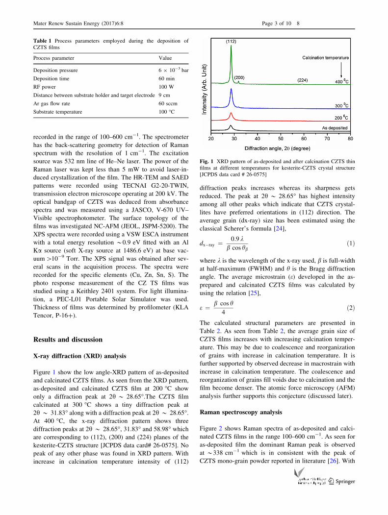
Figure 1 show the low angle-XRD pattern of as-deposited
and calcinated CZTS films. As seen from the XRD pattern,
as-deposited and calcinated CZTS film at 200 �C show
only a diffraction peak at 2h * 28.65�.The CZTS film
calcinated at 300 �C shows a tiny diffraction peak at
2h * 31.83� along with a diffraction peak at 2h * 28.65�.At 400 �C, the x-ray diffraction pattern shows three
diffraction peaks at 2h * 28.65�, 31.83� and 58.98� whichare corresponding to (112), (200) and (224) planes of the
kesterite-CZTS structure [JCPDS data card# 26-0575]. No
peak of any other phase was found in XRD pattern. With
increase in calcination temperature intensity of (112)
diffraction peaks increases whereas its sharpness gets
reduced. The peak at 2h * 28.65� has highest intensity
among all other peaks which indicate that CZTS crystal-
lites have preferred orientations in (112) direction. The
average grain (dx-ray) size has been estimated using the
classical Scherer’s formula [24],
dx�ray ¼ 0:9 kb cos hb
ð1Þ
where k is the wavelength of the x-ray used, b is full-width
at half-maximum (FWHM) and h is the Bragg diffraction
angle. The average microstrain (e) developed in the as-
prepared and calcinated CZTS films was calculated by
using the relation [25],
e ¼ b cos h4
ð2Þ
The calculated structural parameters are presented in
Table 2. As seen from Table 2, the average grain size of
CZTS films increases with increasing calcination temper-
ature. This may be due to coalescence and reorganization
of grains with increase in calcination temperature. It is
further supported by observed decrease in macrostrain with
increase in calcination temperature. The coalescence and
reorganization of grains fill voids due to calcination and the
film become denser. The atomic force microscopy (AFM)
analysis further supports this conjecture (discussed later).
Raman spectroscopy analysis
Figure 2 shows Raman spectra of as-deposited and calci-
nated CZTS films in the range 100–600 cm-1. As seen for
as-deposited film the dominant Raman peak is observed
at *338 cm-1 which is in consistent with the peak of
CZTS mono-grain powder reported in literature [26]. With
Table 1 Process parameters employed during the deposition of
CZTS films
Process parameter Value
Deposition pressure 6 9 10-3 bar
Deposition time 60 min
RF power 100 W
Distance between substrate holder and target electrode 9 cm
Ar gas flow rate 60 sccm
Substrate temperature 100 �C
Fig. 1 XRD pattern of as-deposited and after calcination CZTS thin
films at different temperatures for kesterite-CZTS crystal structure
[JCPDS data card # 26-0575]
Mater Renew Sustain Energy (2017) 6:8 Page 3 of 10 8
123
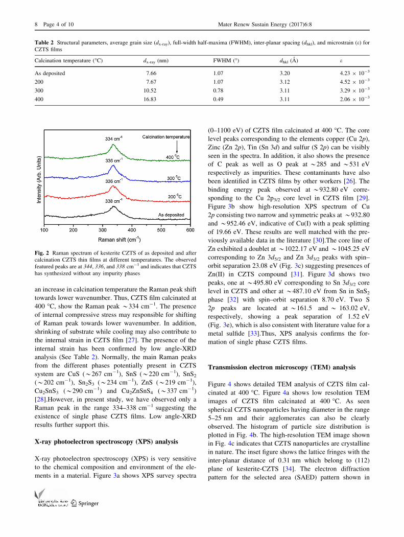
an increase in calcination temperature the Raman peak shift
towards lower wavenumber. Thus, CZTS film calcinated at
400 �C, show the Raman peak *334 cm-1. The presence
of internal compressive stress may responsible for shifting
of Raman peak towards lower wavenumber. In addition,
shrinking of substrate while cooling may also contribute to
the internal strain in CZTS film [27]. The presence of the
internal strain has been confirmed by low angle-XRD
analysis (See Table 2). Normally, the main Raman peaks
from the different phases potentially present in CZTS
system are CuS (*267 cm-1), SnS (*220 cm-1), SnS2(*202 cm-1), Sn2S3 (*234 cm-1), ZnS (*219 cm-1),
Cu2SnS3 (*290 cm-1) and Cu2ZnSnS4 (*337 cm-1)
[28].However, in present study, we have observed only a
Raman peak in the range 334–338 cm-1 suggesting the
existence of single phase CZTS films. Low angle-XRD
results further support this.
X-ray photoelectron spectroscopy (XPS) analysis
X-ray photoelectron spectroscopy (XPS) is very sensitive
to the chemical composition and environment of the ele-
ments in a material. Figure 3a shows XPS survey spectra
(0–1100 eV) of CZTS film calcinated at 400 �C. The core
level peaks corresponding to the elements copper (Cu 2p),
Zinc (Zn 2p), Tin (Sn 3d) and sulfur (S 2p) can be visibly
seen in the spectra. In addition, it also shows the presence
of C peak as well as O peak at *285 and *531 eV
respectively as impurities. These contaminants have also
been identified in CZTS films by other workers [26]. The
binding energy peak observed at *932.80 eV corre-
sponding to the Cu 2p3/2 core level in CZTS film [29].
Figure 3b show high-resolution XPS spectrum of Cu
2p consisting two narrow and symmetric peaks at *932.80
and *952.46 eV, indicative of Cu(I) with a peak splitting
of 19.66 eV. These results are well matched with the pre-
viously available data in the literature [30].The core line of
Zn exhibited a doublet at *1022.17 eV and *1045.25 eV
corresponding to Zn 3d5/2 and Zn 3d3/2 peaks with spin–
orbit separation 23.08 eV (Fig. 3c) suggesting presences of
Zn(II) in CZTS compound [31]. Figure 3d shows two
peaks, one at *495.80 eV corresponding to Sn 3d3/2 core
level in CZTS and other at *487.10 eV from Sn in SnS2phase [32] with spin–orbit separation 8.70 eV. Two S
2p peaks are located at *161.5 and * 163.02 eV,
respectively, showing a peak separation of 1.52 eV
(Fig. 3e), which is also consistent with literature value for a
metal sulfide [33].Thus, XPS analysis confirms the for-
mation of single phase CZTS films.
Transmission electron microscopy (TEM) analysis
Figure 4 shows detailed TEM analysis of CZTS film cal-
cinated at 400 �C. Figure 4a shows low resolution TEM
images of CZTS film calcinated at 400 �C. As seen
spherical CZTS nanoparticles having diameter in the range
5–25 nm and their agglomerates can also be clearly
observed. The histogram of particle size distribution is
plotted in Fig. 4b. The high-resolution TEM image shown
in Fig. 4c indicates that CZTS nanoparticles are crystalline
in nature. The inset figure shows the lattice fringes with the
inter-planar distance of 0.31 nm which belong to (112)
plane of kesterite-CZTS [34]. The electron diffraction
pattern for the selected area (SAED) pattern shown in
Table 2 Structural parameters, average grain size (dx-ray), full-width half-maxima (FWHM), inter-planar spacing (dhkl), and microstrain (e) forCZTS films
Calcination temperature (�C) dx-ray (nm) FWHM (�) dhkl (A) e
As deposited 7.66 1.07 3.20 4.23 9 10-3
200 7.67 1.07 3.12 4.52 9 10-3
300 10.52 0.78 3.11 3.29 9 10-3
400 16.83 0.49 3.11 2.06 9 10-3
Fig. 2 Raman spectrum of kesterite CZTS of as deposited and after
calcination CZTS thin films at different temperatures. The observed
featured peaks are at 344, 336, and 338 cm-1 and indicates that CZTS
has synthesized without any impurity phases
8 Page 4 of 10 Mater Renew Sustain Energy (2017) 6:8
123
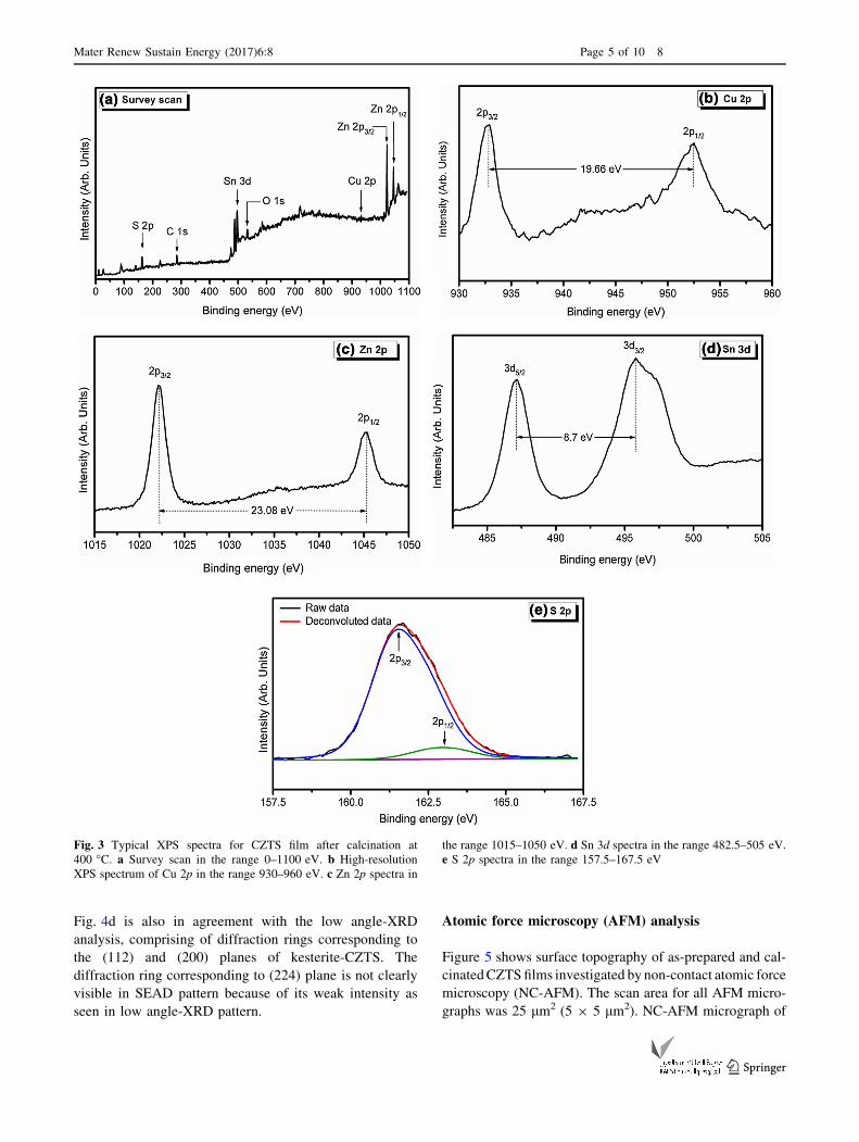
Fig. 4d is also in agreement with the low angle-XRD
analysis, comprising of diffraction rings corresponding to
the (112) and (200) planes of kesterite-CZTS. The
diffraction ring corresponding to (224) plane is not clearly
visible in SEAD pattern because of its weak intensity as
seen in low angle-XRD pattern.
Atomic force microscopy (AFM) analysis
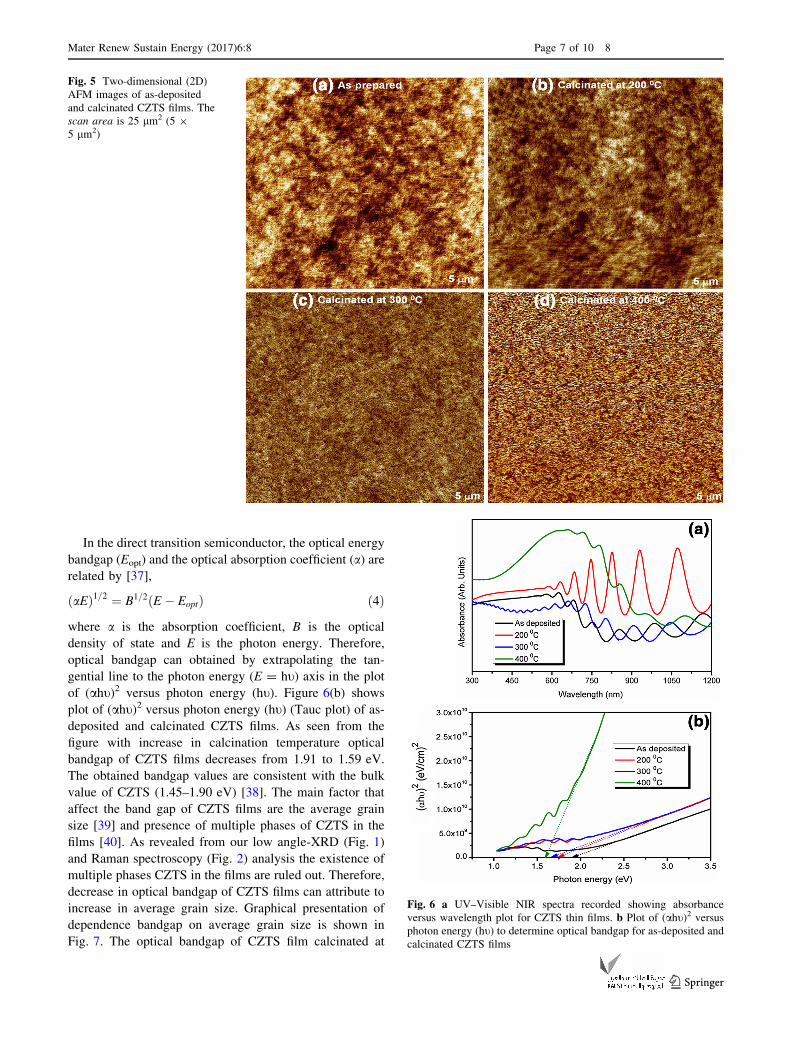
Figure 5 shows surface topography of as-prepared and cal-
cinatedCZTSfilms investigated by non-contact atomic force
microscopy (NC-AFM). The scan area for all AFM micro-
graphs was 25 lm2 (5 9 5 lm2). NC-AFM micrograph of
Fig. 3 Typical XPS spectra for CZTS film after calcination at
400 �C. a Survey scan in the range 0–1100 eV. b High-resolution
XPS spectrum of Cu 2p in the range 930–960 eV. c Zn 2p spectra in
the range 1015–1050 eV. d Sn 3d spectra in the range 482.5–505 eV.
e S 2p spectra in the range 157.5–167.5 eV
Mater Renew Sustain Energy (2017) 6:8 Page 5 of 10 8
123
as-prepared CZTS film revealed textured surface with tiny
uniform island-like topography. It has been reported that
such topography originates from the island growth of the
Volmer-Weber mode and the kinetic energy at low temper-
ature is not sufficient for the coalescence of island-like
crystallites [35]. The root mean square (rms) surface
roughness of as-prepared CZTS film was found *0.32 nm.
The CZTS film calcinated at 200 �C (Fig. 5b) clearly indi-
cate that these tiny textured island coalescence to form super-
structure of smaller clusters with increased rms surface
roughness to *0.76 nm. The coalescence of textured island
may occur due to increase in the surface mobility with
increase in calcination temperature. Further increase in cal-
cination temperature to 300 �C and 400 �C (Fig. 5(c, d) one
can have observed that these smaller clusters of CZTS are
bound together and formed into non-uniform larger clusters
with enhanced surface roughness. Thus, CZTS films calci-
nated at 300 8C and 400 �C the rms surface roughness was
found *0.60 and 3.21 nm respectively. Therefore, from
AFM analysis it has been concluded that with increase in
calcination temperature the particle size and surface rough-
ness of CZTS film increases.
UV–Visible spectroscopy analysis
The optical properties of as-deposited and calcinated CZTS
films were investigated from UV–Visible spectroscopy.
The optical absorption coefficient (a) can be calculated
from the transmittance (T) and reflection (R) of the films
with the formula [36],
a ¼ 1
dln
T
1� R
� �ð3Þ
where d is the thickness of the films. Figure 6a display the
variation of absorbance for as-deposited and calcinated CZTS
thin films.The optical absorption coefficient after calcinations
CZTS films was found[104 cm-1 in the visible region indi-
cating a direct bandgap characteristic of CZTS films.
Fig. 4 a TEM image with low magnification, b particle size
distribution histogram, representing particle size ranging from 5 to
25 nm, c HR-TEM, demonstrating nanoparticles have lattice fringes
with inter-planar distance of 0.31 nm, and d SAED pattern of
concentric rings correspond to three major peaks in XRD of Kesterite-
CZTS nanoparticles
8 Page 6 of 10 Mater Renew Sustain Energy (2017) 6:8
123
In the direct transition semiconductor, the optical energy
bandgap (Eopt) and the optical absorption coefficient (a) arerelated by [37],
ðaEÞ1=2 ¼ B1=2ðE � EoptÞ ð4Þ
where a is the absorption coefficient, B is the optical
density of state and E is the photon energy. Therefore,
optical bandgap can obtained by extrapolating the tan-
gential line to the photon energy (E = ht) axis in the plot
of (aht)2 versus photon energy (ht). Figure 6(b) shows
plot of (aht)2 versus photon energy (ht) (Tauc plot) of as-deposited and calcinated CZTS films. As seen from the
figure with increase in calcination temperature optical
bandgap of CZTS films decreases from 1.91 to 1.59 eV.
The obtained bandgap values are consistent with the bulk
value of CZTS (1.45–1.90 eV) [38]. The main factor that
affect the band gap of CZTS films are the average grain
size [39] and presence of multiple phases of CZTS in the
films [40]. As revealed from our low angle-XRD (Fig. 1)
and Raman spectroscopy (Fig. 2) analysis the existence of
multiple phases CZTS in the films are ruled out. Therefore,
decrease in optical bandgap of CZTS films can attribute to
increase in average grain size. Graphical presentation of
dependence bandgap on average grain size is shown in
Fig. 7. The optical bandgap of CZTS film calcinated at
Fig. 5 Two-dimensional (2D)
AFM images of as-deposited
and calcinated CZTS films. The
scan area is 25 lm2 (5 9
5 lm2)
Fig. 6 a UV–Visible NIR spectra recorded showing absorbance
versus wavelength plot for CZTS thin films. b Plot of (aht)2 versus
photon energy (ht) to determine optical bandgap for as-deposited and
calcinated CZTS films
Mater Renew Sustain Energy (2017) 6:8 Page 7 of 10 8
123
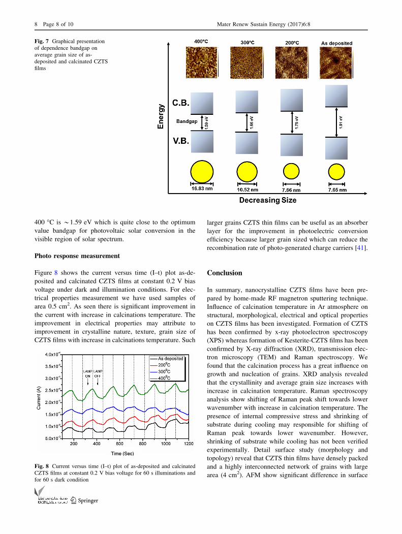
400 �C is *1.59 eV which is quite close to the optimum
value bandgap for photovoltaic solar conversion in the
visible region of solar spectrum.
Photo response measurement
Figure 8 shows the current versus time (I–t) plot as-de-
posited and calcinated CZTS films at constant 0.2 V bias
voltage under dark and illumination conditions. For elec-
trical properties measurement we have used samples of
area 0.5 cm2. As seen there is significant improvement in
the current with increase in calcinations temperature. The
improvement in electrical properties may attribute to
improvement in crystalline nature, texture, grain size of
CZTS films with increase in calcinations temperature. Such
larger grains CZTS thin films can be useful as an absorber
layer for the improvement in photoelectric conversion
efficiency because larger grain sized which can reduce the
recombination rate of photo-generated charge carriers [41].
Conclusion
In summary, nanocrystalline CZTS films have been pre-
pared by home-made RF magnetron sputtering technique.
Influence of calcination temperature in Ar atmosphere on
structural, morphological, electrical and optical properties
on CZTS films has been investigated. Formation of CZTS
has been confirmed by x-ray photoelectron spectroscopy
(XPS) whereas formation of Kesterite-CZTS films has been
confirmed by X-ray diffraction (XRD), transmission elec-
tron microscopy (TEM) and Raman spectroscopy. We
found that the calcination process has a great influence on
growth and nucleation of grains. XRD analysis revealed
that the crystallinity and average grain size increases with
increase in calcination temperature. Raman spectroscopy
analysis show shifting of Raman peak shift towards lower
wavenumber with increase in calcination temperature. The
presence of internal compressive stress and shrinking of
substrate during cooling may responsible for shifting of
Raman peak towards lower wavenumber. However,
shrinking of substrate while cooling has not been verified
experimentally. Detail surface study (morphology and
topology) reveal that CZTS thin films have densely packed
and a highly interconnected network of grains with large
area (4 cm2). AFM show significant difference in surface
Fig. 7 Graphical presentation
of dependence bandgap on
average grain size of as-
deposited and calcinated CZTS
films
Fig. 8 Current versus time (I–t) plot of as-deposited and calcinated
CZTS films at constant 0.2 V bias voltage for 60 s illuminations and
for 60 s dark condition
8 Page 8 of 10 Mater Renew Sustain Energy (2017) 6:8
123
topography of CZTS films with change in calcination
temperature. Increase in calcination temperature show
increase in rms and average surface roughness of the CZTS
films. UV–Visible spectroscopy analysis revealed that the
absorption coefficient of as-deposited and calcinated CZTS
films are in the range 104–105 cm-1 in the visible region.
The bandgap show decreasing trend with increase in cal-
cination temperature (1.91–1.59 eV). The bandgap of
CZTS film annealed at 400 �C was found *1.59 eV which
is quite close to the optimum value for photovoltaic solar
conversion in the visible region of solar spectrum. It is
found that the photo response depends upon the grain size
effect, whereas photo response increases with the increase
of the grain size. Employment these films as an absorber
layer in CZTS solar cells can improve the conversion
efficiency by reducing recombination rate of photo-gener-
ated charge carriers due to increased grain size.
Acknowledgement Mr. Sachin Rondiya is grateful to Dr. Babasaheb
Ambedkar Research and Training Institute (BARTI), Pune for
research fellowship and financial assistance and INUP IITB project
sponsored by DeitY, MCIT, Government of India. Mr. Avinash
Rokade is grateful to MNRE, New Delhi for National Renewable
Energy (NRE) fellowship. One of the authors Dr. Sandesh Jadkar is
thankful to University Grants Commission, New Delhi for special
financial support under UPE program. Mr. Ashok Jadhavar is thankful
to BARC-SSPU program for financial support.
Open Access This article is distributed under the terms of the
Creative Commons Attribution 4.0 International License (http://
creativecommons.org/licenses/by/4.0/), which permits unrestricted
use, distribution, and reproduction in any medium, provided you give
appropriate credit to the original author(s) and the source, provide a
link to the Creative Commons license, and indicate if changes were
made.
References
1. Kalowekamo, J., Baker, E.: Estimating the manufacturing cost of
purely organic solar cells. Sol. Energy 83, 1224–1231 (2009)
2. Steinhagen, C., Panthani, M.G., Akhavan, V., Goodfellow, B.,
Koo, B., Korgel, B.A.: Synthesis of Cu2ZnSnS4 nanocrystals for
use in low-cost photovoltaics. J. Amer. Chem. Soc. 131,12554–12555 (2009)
3. Tanaka, K., Oonuki, M., Moritake, N., Uchiki, H.: Cu2ZnSnS4thin film solar cells prepared by non-vacuum processing. Sol.
Energy Mater. Sol. Cells 93, 583–587 (2009)
4. Katagiri, H., Jimbo, K., Maw, W.S., Oishi, K., Yamazaki, M.,
Araki, H., Takeuchi, A.: Development of CZTS-based thin film
solar cells. Thin Solid Films 517, 2455–2460 (2009)
5. Guo, Q., Hillhouse, H.W., Agrawal, R.: Synthesis of Cu2 Zn Sn
S4 nanocrystal ink and its use for solar cells. J. Amer. Chem. Soc.
131, 11672–11673 (2009)
6. Henry, C.H.: Limiting efficiencies of ideal single and multiple
energy gap terrestrial solar cells. J. Appl. Phys. 51, 4494–4500(1980)
7. Wang, W., Winkler, M.T., Gunawan, O., Gokmen, T., Todorov,
T.K., Zhu, Y., Mitzi, D.B.: Device characteristics of CZTSSe
thin-film solar cells with 12.6% efficiency. Adv. Energy Mater. 4,1301465 (2014)
8. Zeng, X., TaiK, F., Zhang, T., Ho, C., Chen, X., Huan, A., Sum,
T.C., Wong, L.H.: Cu2 Zn Sn (S, Se) 4 kesterite solar cell with
5.1% efficiency using spray pyrolysis of aqueous precursor
solution followed by selenization. Sol. Energy Mater. Sol. Cells
124, 55–60 (2014)
9. Fernandes, P.A., Salome, P.M.P., Cunha, A.F.: Growth and
Raman scattering characterization of Cu2ZnSnS4 thin films. Thin
Solid Films 517, 2519–2523 (2009)
10. Tanaka, K., Moritake, N., Uchiki, H.: Preparation of Cu2 Zn Sn
S4 thin films by sulfurizing sol–gel deposited precursors. Sol.
Energy Mater. Sol. Cells 91, 1199–1201 (2007)
11. Swami, S.K., Kumar, A., Dutta, V.: Deposition of kesterite Cu2Zn Sn S4 (CZTS) thin films by spin coating technique for solar
cell application. Energy Procedia. 33, 198–202 (2013)
12. Todorov, T.K., Reuter, K.B., Mitzi, D.B.: Highefficiency solar
cell with earth-abundant liquid-processed absorber. Adv. Mater.
22, E156–E159 (2010)
13. Mali, S., Patil, P., Hong, C.: Low-cost electrospun highly crys-
talline kesterite Cu2 Zn Sn S4 nanofiber counter electrodes for
efficient dye-sensitized solar Cells. ACS Appl. Mater. Interfaces.
6, 1688–1696 (2014)
14. Mali, S.S., Shinde, P.S., Betty, C.A., Bhosale, P.N., Oh, Y.W.,
Patil, P.S.: Synthesis and characterization of Cu2 Zn Sn S4 thin
films by SILAR method. J. Phys. Chem. Solids 73(6), 735–740(2012)
15. Dhakal, T.P., Peng, C.Y., Tobias, R.R., Dasharathy, R., Westgate,
C.R.: Characterization of a CZTS thin film solar cell grown by
sputtering method. Sol. Energy 100, 23–30 (2014)
16. Lee Y. S., Gershon T., Gunawan O., Todorov T. K., Gokmen T.,
Virgus Y., Guha S.: Adv. Energy Mater. 5, 1401372-1-5 (2015)
17. Sun, L., He, J., Kong, H., Yue, F., Yang, P., Chu, J.: Structure,
composition and optical properties of Cu2 Zn Sn S4 thin films
deposited by pulsed laser deposition method. Sol. Energy Mater.
Sol. Cells 95, 2907–2913 (2011)
18. Wang, J., Li, S., Cai, J., Shen, B., Ren, Y., Qin, G.: Cu2ZnSnS4
thin films: facile and cost-effective preparation by RF-magnetron
sputtering and texture control. J. Alloys Compd. 552, 418–422(2013)
19. Seboui, Z., Gassoumi, A., Cuminal, Y., Turki, N.K.: The post-
growth effect on the properties of Cu2 Zn Sn S4 thin films.
J. Renew. Sus. Energy 7, 011203 (2015)
20. Ericson, T., Scragg, J.J., Kubart, T., Torndahl, T., Bjorkman,
C.P.: Annealing behavior of reactively sputtered precursor films
for Cu2 Zn Sn S4 solar cells. Thin Solid Films 535, 22–26 (2013)
21. Surgina, G.D., Nevolin, V.N., SipayloI, P., Teterin, P.E., Med-
vedeva, S.S., Lebedinsky, Y.Y., Zenkevich, A.V.: Effect of
annealing on structural and optical properties of Cu2 Zn Sn S4thin films grown by pulsed laser deposition. Thin Solid Films
594, 74–79 (2015)
22. Vanalakar, S.A., Shin, S.W., Agawane, G.L., Suryawanshi, M.P.,
Gurav, K.V., Patil, P.S., Kim, J.H.: Effect of post-annealing
atmosphere on the grain-size and surface morphological proper-
ties of pulsed laser deposited CZTS thin films. Ceram. Int. 40,15097–15103 (2014)
23. Liu, R., Tan, M., Zhang, X., Chen, J., Song, S., Zhang, W.:
Impact of sol-gel precursor treatment with preheating tempera-
ture on properties of Cu2 Zn Sn S4 thin film and its photovoltaic
solar cell. J. Alloys Compd. 655, 124–129 (2016)
24. Cullity, B.D., Stock, S.: Elements of X-ray Diffraction, 3rd edn.
Princeton Hall, New Jersey (2001)
25. Girija, K., Thirumalairajan, S., Mohan, S., Chandrasekaran, J.:
Structural, morphological and optical studies of CdSe thin films
from ammonia bath. Chalcog. Lett. 6(8), 351–357 (2009)
Mater Renew Sustain Energy (2017) 6:8 Page 9 of 10 8
123
26. Su, Z., Sun, K., Han, Z., Cui, H., Liu, F., Lai, Y., Li, J., Hao, X.,
Liu, Y., Green, M.A.: Fabrication of Cu2 Zn Sn S4 solar cells with
5.1% efficiency via thermal decomposition and reaction using a
non-toxic sol–gel route. J. Mate. Chem. 2(2), 500–509 (2014)
27. Yoo, H., Kim, J.: Comparative study of Cu2 Zn Sn S4 film
growth. Sol. Energy Mater. Sol. Cells 95(1), 239–244 (2011)
28. Khadka, D.B., Kim, J.: Band gap engineering of alloyed Cu2 Zn
Gex Sn1–x Q4 (Q = S, Se) films for solar cell. J. Phys. Chem. C
119(4), 1706–1713 (2015)
29. Moulder, J.F., Chastain, J.: Handbook of x-ray photoelectron
spectroscopy. In: Eden, P. (ed.) A reference book of standard
spectra for identification and interpretation of XPS data. Perkin-
Elmer Corp, Chanhassen (1992)
30. Zou, C., Zhang, L., Lin, D., Yang, Y., Li, Q., Xu, X., Chen, X.,
Huang, S.: Facile synthesis of Cu2 Zn Sn S4 nanocrystals. Cryst.
Eng. Comm. 13(10), 3310–3313 (2011)
31. Sun, Y., Zhang, Y., Wang, H., Xie, M., Zong, K., Zheng, H., Shu,
Y., Liu, J., Yan, H., Zhu, M.: Novel non-hydrazine solution
processing of earth-abundant Cu2 Zn Sn (S, Se)4 absorbers for
thin-film solar cells. J. Mate. Chem. A 1(23), 6880–6887 (2013)
32. Khelia, C., Boubaker, K., Ben, Nasrallah T., Amlouk, M., Bel-
gacem, S.: Morphological and thermal properties of b-SnS2sprayed thin films using Boubaker polynomials expansion. J. Al-
loys Compd. 477, 461–467 (2009)
33. Su, Z., Sun, K., Han, Z., Liu, F., Lai, Y., Li, J., Liu, Y.: Fabri-
cation of ternary Cu-Sn-S sulfides by a modified successive ionic
layer adsorption and reaction (SILAR) method. J. Mate. Chem.
22(32), 16346–16352 (2012)
34. Lu, X., Zhuang, Z., Peng, Q., Li, Y.: Wurtzite Cu2ZnSnS4nanocrystals: a novel quaternary semiconductor. Chem. Comm.
47(11), 3141–3143 (2011)
35. Shah, N., Panchal, C., Kheraj, V., Ray, J., Desai, M.: Growth,
structural and optical properties of copper indium diselenide thin
films deposited by thermal evaporation method. Sol. Energy
83(5), 753–760 (2009)
36. Muth, J.F., Lee, J.H., Shmagin, I.K., KolbasH, R.M., Casey, C.,
Keller, B.P., Mishra, U.K., Den Baars, S.P.: Absorption coeffi-
cient, energy gap, exciton binding energy, and recombination
lifetime of GaN obtained from transmission measurements. Appl.
Phys. Lett. 71(18), 2572–2574 (1997)
37. Tauc, J.: Absorption edge and internal electric fields in amor-
phous semiconductors. Mater. Res. Bull. 5(8), 721–729 (1970)
38. Katagiri, H.: Cu2ZnSnS4 thin film solar cells. Thin Solid Films
480, 426–432 (2005)
39. Liu, W., Guo, B., Wu, X., Zhang, F., Mak, C., Wong, K.: Facile
hydrothermal synthesis of hydrotropic Cu2ZnSnS4 nanocrystal
quantum dots: band-gap engineering and phonon confinement
effect. J. Mate. Chem. A 1(9), 3182–3186 (2013)
40. Shin, S.W., Pawar, S.M., Park, C.Y., Yun, J.H., Moon, J.H., Kim,
J.H., Lee, J.Y.: Studies on Cu2ZnSnS4 (CZTS) absorber layer
using different stacking orders in precursor thin films. Sol.
Energy Mater. Sol. Cells 95(12), 3202–3206 (2011)
41. Persson, C.: Electronic and optical properties of Cu2 Zn Sn S4 and
Cu2 Zn Sn Se4. J. Appl. Phys. 107, 710 (2010)
8 Page 10 of 10 Mater Renew Sustain Energy (2017) 6:8
123
Related Documents


