EECE476 Lecture 9: Multi-cycle CPU Datapath Chapter 5: Section 5.5 The University of British Columbia EECE 476 © 2005 Guy Lemieux

EECE476 Lecture 9: Multi-cycle CPU Datapath Chapter 5: Section 5.5 The University of British ColumbiaEECE 476© 2005 Guy Lemieux.
Dec 20, 2015
Welcome message from author
This document is posted to help you gain knowledge. Please leave a comment to let me know what you think about it! Share it to your friends and learn new things together.
Transcript
EECE476
Lecture 9: Multi-cycle CPU Datapath
Chapter 5: Section 5.5
The University ofBritish Columbia EECE 476 © 2005 Guy Lemieux

2
Overview
• Last week– 1-cycle CPU datapath– 1-cycle CPU controller (lookup table, no state)
• Today– Multi-cycle CPU datapath
• Tomorrow– Multi-cycle CPU controller (contains state!)

3
1-cycle CPU Datapath + Controller
Error in TextFig 5.24Instruction
[31:26]
Instruction[25:0]
PC + 4 [31..28]
Jump address [31..0]
Instruction[25:21]
Instruction[20:16]
Instruction[15:11]
Instruction[15:0]
Instruction[5:0]

4
1-cycle CPU Summary• Operation
– 1 cycle per instruction– Control signals held fixed during entire cycle (except BRANCH)– Only 2 registers
• PC, updated every clock cycle• REGFILE, updated when required
– During clock cycle, data flows from register-outputs to register-inputs– Fixed clock frequency / period
• Performance– 1 instruction per cycle– Slowest instruction determines clock frequency
• Outstanding issue: MemWrite timing– Assume this signal writes to memory at end of clock cycle
5
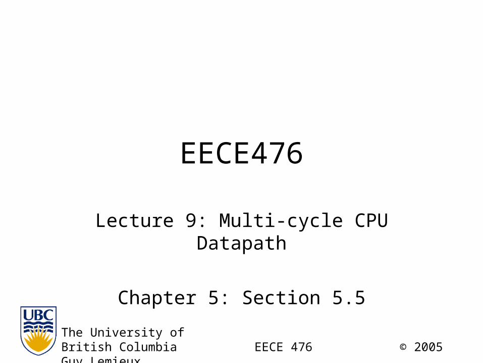
Multi-cycle CPU Goals• Improve performance
– Break each instruction into smaller steps / multiple cycles• LW instruction 5 cycles• SW instruction 4 cycles• R-type instruction 4 cycles• Branch, Jump 3 cycles
– Aim for 5x clock frequency• Complex instructions (eg, LW) 5 cycles same performance as before• Simple instructions (eg, ADD) fewer cycles faster
• Save resources (gates/transistors)– Re-use ALU over multiple cycles– Put INSTR + DATA in same memory
• MemWrite timing solved?

6
Multi-cycle CPU Datapath
Instruction[25:21]
Instruction[20:16]
Instruction[15:11]
Instruction[15:0]
Instruction[5:0]
Instr[15:0]
InstructionRegister
MemoryData
Register
ALUOut
A
B
MemoryMemData
Address
Writedata
Registers
RdData1
RdData2
RdReg2
RdReg1
Writereg
Writedata
• Add multiplexers + control signals (IorD, MemtoReg, ALUSrcA, ALUSrcB)• Move signal paths (+4, Shift Left 2)
4
ShiftLeft 2
SignExtend
PC
Mux
Mux
ALU
ALUresult
Zero
Mux
Mux
Mux

7
Multi-cycle CPU Datapath
Instruction[25:21]
Instruction[20:16]
Instruction[15:11]
Instruction[15:0]
Instruction[5:0]
Instr[15:0]
ALUOut
A
B
MemoryMemData
Address
Writedata
Registers
RdData1
RdData2
RdReg2
RdReg1
Writereg
Writedata
• Add registers + control signals (IR, MDR, A, B, ALUOut)– Registers with no control signal load value every clock cycle (eg, PC)
4
ShiftLeft 2
SignExtend
PC
Mux
Mux
ALU
ALUresult
Zero
Mux
Mux
Mux
InstructionRegister
MemoryData
Register

8
Instruction Execution Example
• Execute a “Load Word” instruction– LW rt, 0(rs)
• 5 Steps1. Fetch instruction2. Read registers3. Compute address4. Read data5. Write registers
9
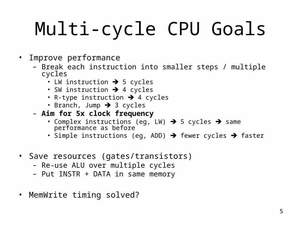
Load Word Instruction Trace
1. Fetch InstructionInstructionRegister ← Mem[PC]
Instruction[25:21]
Instruction[20:16]
Instruction[15:11]
Instruction[5:0]
Instr[15:0]
ALUOut
A
BWritedata
Registers
RdData1
RdData2
RdReg2
RdReg1
Writereg
Writedata
4
ShiftLeft 2
SignExtend
PC
Mux
Mux
ALU
ALUresult
Zero
Mux
Mux
Mux
InstructionRegister
MemoryData
Register
Instruction[15:0]
MemoryMemData
Address

10
Load Word Instruction Trace
2. Read RegistersA ← Registers[Rs]
Instruction[20:16]
Instruction[15:11]
Instruction[15:0]
Instruction[5:0]
Instr[15:0]
ALUOut
A
B
MemoryMemData
Address
Writedata
Registers
RdData2
RdReg2
Writereg
Writedata
4
ShiftLeft 2
SignExtend
PC
Mux
Mux
ALU
ALUresult
Zero
Mux
Mux
Mux
InstructionRegister
MemoryData
Register
Instruction[25:21]
RdData1
RdReg1

11
Load Word Instruction Trace
3. Compute AddressALUOut ← A + {SignExt(Imm16),b’00’}
Instruction[25:21]
Instruction[20:16]
Instruction[15:0]
Instruction[5:0]
Instr[15:0]
B
MemoryMemData
Address
Writedata
Registers
RdData1
RdData2
RdReg2
RdReg1
Writereg
Writedata
4
ShiftLeft 2
SignExtend
PC
Mux
Mux
ALU
ALUresult
Zero
Mux
Mux
Mux
InstructionRegister
MemoryData
Register
Instruction[15:11]
ALUOut
A

12
Load Word Instruction Trace
4. Read DataMDR ← Memory[ALUOut]
Instruction[25:21]
Instruction[20:16]
Instruction[15:11]
Instruction[15:0]
Instruction[5:0]
Instr[15:0]
A
BWritedata
Registers
RdData1
RdData2
RdReg2
RdReg1
Writereg
Writedata
4
ShiftLeft 2
SignExtend
PC
Mux
Mux
ALU
ALUresult
Zero
Mux
Mux
Mux
InstructionRegister
MemoryData
Register
ALUOut
MemoryMemData
Address

13
Load Word Instruction Trace
5. Write RegistersRegisters[Rt] ← MDR
Instruction[25:21]
Instruction[20:16]
Instruction[15:11]
Instruction[15:0]
Instruction[5:0]
Instr[15:0]
ALUOut
A
B
MemoryMemData
Address
Writedata
Registers
RdData1
RdData2
RdReg2
RdReg1
4
ShiftLeft 2
SignExtend
PC
Mux
Mux
ALU
ALUresult
Zero
Mux
Mux
Mux
InstructionRegister
MemoryData
Register
Writereg
Writedata

14
Load Word Instruction Trace
All 5 Steps Shown
Instruction[5:0]
Instr[15:0]
BWritedata
Registers
RdData2
RdReg2
4
ShiftLeft 2
SignExtend
PC
Mux
Mux
ALU
ALUresult
Zero
Mux
Mux
Mux
InstructionRegister
MemoryData
Register
Instruction[25:21]
Instruction[20:16]
Instruction[15:11]
Instruction[15:0]
ALUOut
MemoryMemData
AddressRdData1
RdReg1
Writereg
Writedata
A

15
Multi-cycle Load Word: Recap1. Fetch InstructionInstructionRegister ← Mem[PC]
2. Read Registers A ← Registers[Rs]
3. Compute Address ALUOut ← A + {SignExt(Imm16)}
4. Read Data MDR ← Memory[ALUOut]
5. Write Registers Registers[Rt] ← MDR
• Missing Steps?–

16
Multi-cycle Load Word: Recap1. Fetch InstructionInstructionRegister ← Mem[PC]; PC ← PC + 4
2. Read Registers A ← Registers[Rs]
3. Compute Address ALUOut ← A + {SignExt(Imm16)}
4. Read Data MDR ← Memory[ALUOut]
5. Write Registers Registers[Rt] ← MDR
• Missing Steps?– Must increment the PC– Do it as part of the instruction fetch (in step 1)– Need PCWrite control signal
17
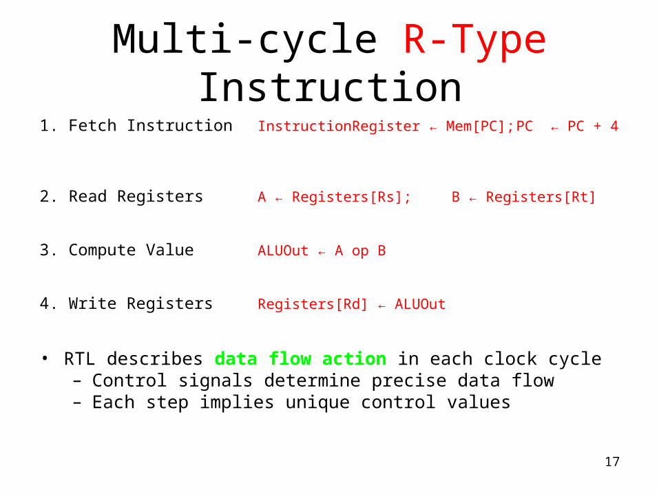
Multi-cycle R-Type Instruction1. Fetch Instruction InstructionRegister ← Mem[PC]; PC ← PC + 4
2. Read Registers A ← Registers[Rs]; B ← Registers[Rt]
3. Compute Value ALUOut ← A op B
4. Write Registers Registers[Rd] ← ALUOut
• RTL describes data flow action in each clock cycle– Control signals determine precise data flow– Each step implies unique control values

18
Multi-cycle R-Type Instruction: Control Signal Values
1. Fetch Instruction InstructionRegister ← Mem[PC]; PC ← PC + 4MemRead=1, ALUSrcA=0, IorD=0, IRWrite, ALUSrcB=01, ALUop=00, PCWrite, PCSource=00
2. Read Registers A ← Registers[Rs]; B ← Registers[Rt]ALUSrcA=0, ALUSrcB=11, ALUop=00
3. Compute Value ALUOut ← A op BALUSrcA=1, ALUSrcB=00, ALUop=10
4. Write Registers Registers[Rd] ← ALUOutRegDst=1, RegWrite, MemtoReg=0
• Each step implies unique control values– Fixed for entire cycle– “Default value” implied if unspecified

19
Check Your Work – Is RTL Valid ? Easy as 1-2-3 !
1. Datapath check– Within one cycle…
• Each cycle has valid data flow path (path exists)• Each register gets only one new value
– Across multiple cycles…• Register value is defined before use in previous (earlier in time) clock cycle
– Eg, “A 3” must occur before “B A”• Make sure register value doesn’t disappear if set >1 cycle earlier
2. Control signal check– Each cycle, RTL describing the datapath flow implies a value for each
control signal• 0 or 1 or default or don’t care
– Each control signal gets only one fixed value the entire cycle
3. Overall check– Does the sequence of steps work ??

20
Multi-cycle BEQ Instruction
1. Fetch InstructionInstructionRegister ← Mem[PC]; PC ← PC + 4
2. Read Registers, Precompute TargetA ← Registers[Rs] ; B ← Registers[Rt] ; ALUOut ← PC + {SignExt{Imm16},b’00’}
3. Compare Registers, Conditional Branchif( (A – B) ==0 ) PC ← ALUOut
Green shows PC calculation flow (in parallel with other operations)
HOMEWORK FOR TOMORROWPrint out datapath diagram & ensure RTL is Valid !Determine control signal value for each cycle !!
21
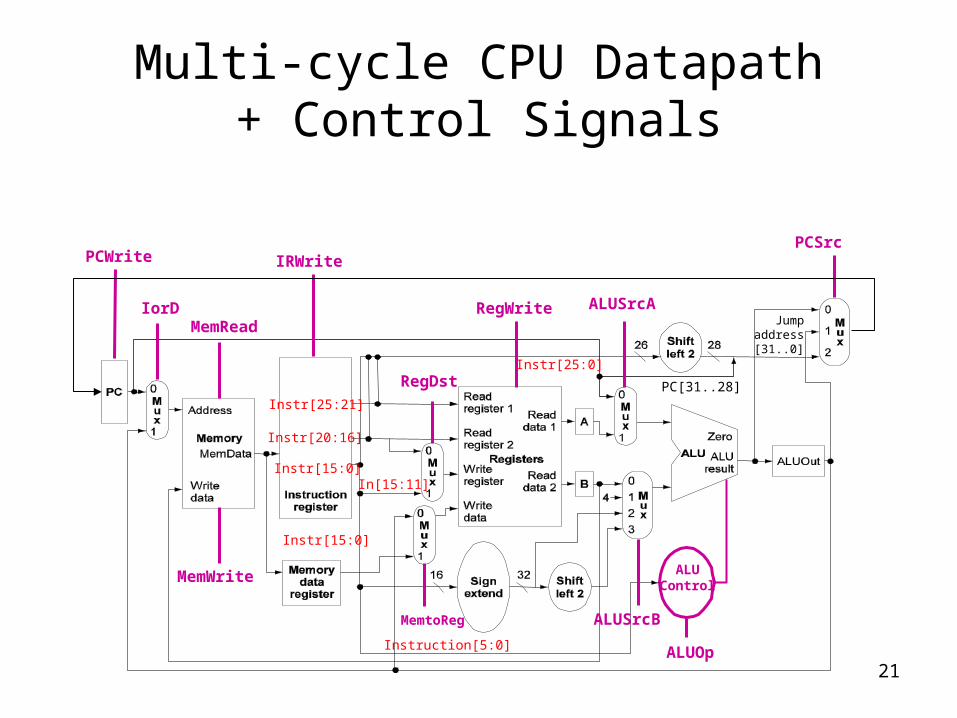
Multi-cycle CPU Datapath+ Control Signals
Instr[25:21]
Instr[20:16]
Instr[15:0]
Instr[15:0]
Instruction[5:0]
In[15:11]
Instr[25:0]
PC[31..28]
Jumpaddress
[31..0]
PCWrite
IorDMemRead
MemWrite
MemtoReg
IRWritePCSrc
ALUOp
ALUSrcA
ALUSrcB
RegWrite
RegDst
ALUControl

22
Multi-cycle CPU Datapath+ Controller
Instr.[31:26]
Instr[31:26]
Instr[25:21]
Instr[20:16]
Instr[15:0]
Instr[15:0]
Instruction[5:0]
In[15:11]
Instr[25:0]
PC[31..28]
Jumpaddress
[31..0]
Related Documents