EDI Functional Test – Procedure 3/23/11 1:38 PM ! Created by B. Anderson after going through the procedure once with D. McGaw and taking notes. Required Equipment • EDI Board • Test Cables o J1: Male 26 Pin Connector with 3 wires ! Red in pin 1 (other end is banana clip) ! White in pin 10 (other end is banana clip) ! Black in pin 19 (other end is banana clip) o J2: Male 44 Pin Connector with 8 wires ! Blue in pins 1, 16 (other ends are open wires) ! Green in pins 2, 17 (other ends are open wires) ! Purple in pins 3, 18 (other ends are open wires) ! Red in pin 31 (other end is banana clip) ! Black in pin 32 (other end is banana clip) • Static mat with grounding strap • Wrist grounding strap • 4 power supplies (at least two with current limiting capability for the CTSPS and VTSPS) • 3 multimeters capable of making high precision volt measurements o One is for diagnostics, in case voltages need to be tested on the fly. • Alligator and banana clip wires • Small jewelers flathead screwdriver • Interface Breadboard with the proper circuitry (I do not have a copy of the schematic diagram of the breadboard as I create this document) • Big rainbow ribbon cable from EDI to IB • Resistors: one each of 10 and 1000 ohm (for voltage divider) • Data sheet: for recording the results of the functional test and the calibrations scale factors. Symbols ! Question marks signify steps for which I do not have instructions or schematic diagrams. ! Blue boxes signify steps for which you have to check or redo the Test Source Power Supply circuitry to the J1 or J2 test dangles.

Welcome message from author
This document is posted to help you gain knowledge. Please leave a comment to let me know what you think about it! Share it to your friends and learn new things together.
Transcript

EDI Functional Test – Procedure 3/23/11 1:38 PM
!"
"
Created by B. Anderson after going through the procedure once with D. McGaw and taking notes.
Required Equipment
• EDI Board
• Test Cables
o J1: Male 26 Pin Connector with 3 wires
! Red in pin 1 (other end is banana clip)
! White in pin 10 (other end is banana clip)
! Black in pin 19 (other end is banana clip)
o J2: Male 44 Pin Connector with 8 wires
! Blue in pins 1, 16 (other ends are open wires)
! Green in pins 2, 17 (other ends are open wires)
! Purple in pins 3, 18 (other ends are open wires)
! Red in pin 31 (other end is banana clip)
! Black in pin 32 (other end is banana clip)
• Static mat with grounding strap
• Wrist grounding strap
• 4 power supplies (at least two with current limiting capability for
the CTSPS and VTSPS)
• 3 multimeters capable of making high precision volt measurements
o One is for diagnostics, in case voltages need to be tested on
the fly.
• Alligator and banana clip wires
• Small jewelers flathead screwdriver
• Interface Breadboard with the proper circuitry (I do not have a copy
of the schematic diagram of the breadboard as I create this
document)
• Big rainbow ribbon cable from EDI to IB
• Resistors: one each of 10 and 1000 ohm (for voltage divider)
• Data sheet: for recording the results of the functional test and the
calibrations scale factors.
Symbols
! Question marks signify steps for which I do not have instructions or
schematic diagrams.
! Blue boxes signify steps for which you have to check or redo the Test
Source Power Supply circuitry to the J1 or J2 test dangles.

#"
"
! Green boxes signify the beginning of a set of steps that will later be
repeated.
! Red boxes signify the end of a set of steps that will later be repeated
! Exclamation points signify steps for which you need to record a value or
observation on the data sheet.
Important—I do not have the know-how to trouble shoot the EDI board. If
a problem with the EDI board is diagnosed or found, you need to ask David
McGaw to investigate and fix if possible.
Procedure
1. Review this procedure and become familiar with the purpose of this
test, the logic conventions for each switch, and the nuances of the
way the IB lights work.
2. Put on your grounding wrist strap as soon as the static mat is
properly set up and grounded.
3. Setup the Test Jig (everything except the EDI board) on the static
mat without turning anything on. There is no schematic diagram
for the IB or the big rainbow ribbon cable from the EDI to the IB,
but as long as nothing happens to the version of these that are
already in place, we’ll be fine. Follow the schematics for connecting
the EDI Power Supplies to the EDI and the Test Source Power
Supplies to the J1 and J2 test dangles.
i. See Photos 1, 5, 6, and 9
4. Set up the IB by insuring the switches are set as:
i. BAS=0030
ii. CS=all up, except right-most bit (bit 0, labeled as switch 1) is
down
1. i.e. IAES=up/off
2. i.e. RS=up/off
3. Note: The only two bits on the CS that will be changed
during this are the IAES and RS.
iii. WS=down/off
iv. IAS=00

$"
"
5. Without connecting the EDI board to anything, turn on the EDI
Power Supplies and insure with a multimeter that the voltages they
supply are correct.
i. At this time, the wires on the big rainbow ribbon cable need to
be wired as:
1. Red = +5V
2. Green = ground
3. Black = -5V
ii. To make it consistent with the normal scheme for the rest of
the payload, David McGaw may at some point change the
wiring to be:
1. Red = +5V
2. Black = ground
3. Green = -5V
6. Turn off EDI Power Supplies.
7. Without the J1 or J2 test dangles being connected to the EDI, set
up the Test Source Power Supplies and insure they are providing
the proper CTSPSV and VTSPSV required.
i. Note that the CTSPSV will always be set to 50.00 mV.
1. Use a voltage divider as shown in the schematics.
ii. Note that you can set the VTSPSV to 10.000V since that is the
first HSV that we will be testing.
iii. Note also that changing the VTSPSV will cause the CTSPSV to
change as well. This is just important to be aware of.
iv. IMPORTANT: Current limit each Test Source Power Supply to
10 mA.
8. Connect the J1 test dangle into the Test Source Power Supplies:
i. White = plus of VTSPS
ii. Black = minus of VTSPS
iii. Red = plus of CTSPS
9. Turn off the Test Source Power Supplies.
10. Prepare the EDI board to be tested. Place EDI on static mat. Do
not plug anything in. Insure jumper shorts are placed on slots 3, 6,
7, 8, 9, 10. This correctly sets the “address select” for the EDI
board.
i. See Photo 2
11. Connect the EDI to the test jig by plugging the big rainbow
ribbon cable into the EDI.

%"
"
12. Turn on the EDI Power Supplies.
13. Turn on power to the IB.
14. Check that the currents on the EDI Power Supplies are nominal
i. ~30 mA on the +5V
ii. ~0 mA on the -5V
15. If this is the first time the EDI board has been turned on or used,
its programmable logic chip needs to be programmed. Use a PC
computer and use the Lattice ISP interface. David McGaw knows
how to do this, I do not know the details here.
16. Check that the currents on the EDI Power Supplies are nominal
i. ~20 mA on the +5V
ii. ~0 mA on the -5V
17. Turn on the Test Source Power Supplies.
18. VTSPSV = 10.000 V (use high resolution multimeter)
i. Note that this is because the first HSV (V0) is 10 V
19. CTSPSV = 50.00 mV (use high resolution multimeter)
i. Note that this is because the first (and all) HSV for the currents
is 50.00 mV.
20. BAS=0030
i. Note that this allows us to access the input address on the EDI
21. IAS=00
i. Note that this is because we are first testing V0, which has the
Input Address of “00”.
22. IAES=down/on
i. Note that this enables us to write the IAS to the EDI.
23. Verify that the right-most 8 IB Lights display the IAS address
correctly.
i. Note: in this case, all the lights will be off.
24. WS=up/on
25. WS=down/off (just flick the WS on then off)
26. IAES=up/off
27. RS=down/on
28. Verify that the right-most 8 IB Lights display the IAS address
that was just written to the EDI.
i. Note: in this case, all the lights will be off.
29. RS=up/off
30. BAS=0031
i. Note that this allows us to access the ADC data

&"
"
31. RS=down/on
i. Note that this displays the most recent ADC data for the Input
Address you have selected.
32. WS=up/on
i. Note that the ADC is now running continually, and the lights
will flicker in real time as the ADC outputs different values.
Changing the VTSPSV will cause the digital output, and hence
the lights, to change. Also the small amount of noise in the
signal causes the very fast fluctuations of small magnitude in
the digital output.
33. Verify that the IB Lights are NOT lighting up.
i. The J1 test dangle is not plugged in, so no lights should be lit
up. If lights light up, there is a problem.
ii. If a few right-most lights light up, that can be okay, as long as
it just looks like noise, and not a problem with the circuitry on
the EDI.
o Plug in the J1 test dangle exactly as in Photo 7, with the test
voltage leads plugging into the furthest-right holes in the EDI
(so that the J1 test dangle frame lines up exactly with the EDI
pin-out frame.)
iii. Now the IB lights should be on and displaying the ADC output.
34. THIS STEP WILL ONLY BE DONE ONCE PER EDI BOARD.
i. Verify the VTSPSV is exactly 10.000 V with the high resolution
multimeter
ii. With the small screwdriver, gently twist the lead on the
potentiometer on the EDI board so that the IB lights display
HSV.
iii. The EDI board is now calibrated. Do not touch the
potentiometer again.
35. Record the VTSPSV HSV value for V0 (10.000 V) on the data
sheet.
36. WS=down/off
37. RS=up/off
38. BAS=0030
39. IAS=10
i. Note that now we’ll be testing the I0 input.
40. IAES=down/on

'"
"
41. Verify that the right-most 8 IB Lights display the IAS address
correctly.
42. WS=up/on
43. WS=down/off
44. IAES=up/off
45. RS=down/on
46. Verify that the right-most 8 IB Lights display the IAS address
that was just written to the EDI.
47. RS=up/off
48. BAS=0031
49. RS=down/on
50. WS=up/on
51. Adjust the CTSPSV to display HSV on the IB Lights
52. Record the CTSPSV HSV value for I0 on the data sheet, use the
reading off of the multimeter for the CTSPSV.
53. WS=down/off
54. RS=up/off
55. You have now verified and calibrated V0 and I0. Now we move
on to V1 and I1. This next part will be quite similar to steps 18-57,
and I will now only refer to switches as being on or off.
56. BAS=0030
57. IAS=01
58. IAES=on
59. Verify the lights correctly display the IAS
60. WS=on then off
61. IAES=off
62. RS=on
63. Verify the lights correctly display what was just written
64. RS=off
65. BAS=0031
66. RS=on
67. WS=on
68. Verify the lights are all off, (except maybe a few of the right-
most bits) since J1 test dangle is not plugged in to the correct
location. If lights are on, there is a problem.
69. Change the VTSPSV if necessary
i. Check to see what the next FSV is for the next voltage input.
ii. Pull the J1 test dangle out of the EDI.

("
"
iii. Adjust the VTSPSV to roughly the HSV for the next voltage
input.
70. Carefully plug the J1 test dangle into the next input on the EDI.
i. Move the test dangle over one column of pins from the
previous placement, as demonstrated in Photos 7 and 8.
ii. The IB lights should be lit, now.
71. Adjust the VTSPSV so the lights read HSV.
72. Record the VTSPSV HSV reading off the high resolution
multimeter on the data sheet.
73. WS=off
74. RS=off
75. BAS=0030
76. IAS=11
77. IAES=on
78. Verify the lights correctly display the IAS
79. WS=on then off
80. IAES=off
81. RS=on
82. Verify the lights correctly display what was just written
83. RS=off
84. BAS=0031
85. RS=on
86. WS=on
87. Adjust the CTSPSV so the lights display HSV
88. Record the CTSPSV HSV reading off the high resolution
multimeter on the data sheet. Make sure to get 4 sig figs.
Depending on the multimeter, you may need to bring the CTSPSV
way down, let the multimeter readjust to get a high resolution
reading, and then bring CTSPSV back up to ~50 mV.
89. WS=off
90. RS=off
91. Repeat steps 57 through 91 for V2 and I2 through V5 and I5.
i. Adjust steps 58 and 77 accordingly
1. V2 and I2: IAS=02 and IAS=12
2. V3 and I3: IAS=03 and IAS=13
3. V4 and I4: IAS=04 and IAS=14
4. V5 and I5: IAS=05 and IAS=15

)"
"
ii. Be very careful not to put an out of range voltage into any
input!
92. Remove the J1 test dangle from the EDI.
93. Turn off the CTSPS and the VTSPS and rewire the Test Source
Power Supplies to J1 test dangle circuit for V6 and I6 and V7 and I7
inputs following the schematics provided.
94. Reconnect the J1 test dangle to the Test Source Power Supplies
but do not plug into EDI.
95. Turn on the CTSPS and VTSPS and set roughly to the next HSVs.
96. Repeat steps 57 through 91 for V6 and I6 and V7 and I7.
i. Adjust steps 58 and 77 accordingly
1. V6 and I6: IAS=06 and IAS=16
2. V7 and I7: IAS=07 and IAS=17
ii. Be very careful not to put the J1 connector into the wrong input
on the EDI!
97. Remove the J1 test dangle from the EDI.
98. Turn the CTSPS and the corresponding multimeter off. You will
not need them again.
99. Turn off the VTSPS and rewire the VTSPS to J2 test dangle
circuit for V8 through V11 following the schematics provided.
i. You’ll be using the red and black wires at this point.
100. Connect the J2 test dangle to the VTSPS circuit, but do not plug
it into the EDI.
101. Turn on the VTSPS and set to roughly the next HSV.
102. BAS=0030
103. IAS=08
104. IAES=on
105. Verify the lights correctly display the IAS
106. WS=on then off
107. IAES=off
108. RS=on
109. Verify the lights correctly display what was just written
110. RS=off
111. BAS=0031
112. RS=on
113. WS=on

*"
"
114. Verify the lights are all off, (except maybe a few of the right-
most bits) since the J2 test dangle is not plugged into to the correct
location (if plugged in at all). If lights are on, there is a problem.
115. Change the VTSPSV if necessary
i. Check to see what the next FSV is for the next voltage input.
ii. Pull the J2 test dangle out of the EDI (if it was in)
iii. Adjust the VTSPSV to the HSV for the next voltage input.
116. Carefully plug the J2 test dangle into the appropriate input on
the EDI.
i. For V8, it’ll be exactly as in Photo 10, with the test voltage
leads plugging into the furthest-right holes in the EDI (so that
the test dangle frame lines up exactly with the EDI pin-out
frame.)
ii. For subsequent inputs, move the J2 test dangle over TWO
columns each time, as in Photos 10 and 11.
iii. The IB Lights should be lit, now.
117. Adjust the VTSPSV so the lights read HSV.
118. Record the VTSPSV HSV reading off the high resolution
multimeter on the data sheet.
119. WS=off
120. RS=off
121. Repeat steps 102 through 120 for V9 through V11.
i. Adjust step 103 accordingly
1. V9: IAS=09
2. V10: IAS=0a
3. V11: IAS=0b
ii. Be very careful not to put the J2 connector into the wrong input
on the EDI!
122. Now we move on to testing the T0 through T15 inputs, still using
the J2 test dangle, but now utilizing the green, purple, and blue
wires.
i. Important: Note that on the J2 test dangle, there are two rows
of blue/green/purple wires. For T0 through T7 use the top row
and for T8 through T15 use the middle row. See Photo 9.
123. Unplug the J2 test dangle from the EDI.
124. Turn off the VTSPS and rewire the VTSPS to J2 test dangle
circuit for T0 through T6 following the schematics provided.

!+"
"
i. Be sure to wire in the blue and green wires from the top row of
the J2 test dangle, not from the middle row.
125. Connect the J2 test dangle to the VTSPS circuit, but do NOT plug
into EDI.
126. Turn on the VTSPS and set to roughly the next HSV: 2.500 V.
i. Note that all the rest of the HSVs will be 2.500 V.
ii. However, now we should have a pull-up on each input T0
through T12. We will have to check and verify the pull-up now,
including that the pull-up is not present for T13 through T15.
127. BAS=0030
128. IAS=20
129. IAES=on
130. Verify the lights correctly display the IAS
131. WS=on then off
132. IAES=off
133. RS=on
134. Verify the lights correctly display what was just written
135. RS=off
136. BAS=0031
137. RS=on
138. WS=on
139. Verify all the lights display FSV. All of the left-most lights should
be lit. This shows the pull-up of 5 V. If the lights are not all lit up,
there is a problem.
140. Record whether or not there was a pull-up for the given input.
141. Insure the VTSPSV is still roughly 2.500 V.
142. Carefully plug the J2 test dangle into the appropriate input on
the EDI.
i. For T0, it’ll be exactly as in Photo 10,"with the test voltage leads
plugging into the furthest-right holes in the EDI (so that the
test dangle frame lines up exactly with the EDI pin-out frame.)
ii. For subsequent inputs, move the J2 test dangle over TWO
columns each time, as in Photos 10 and 11.
143. The IB Lights should be lit to show roughly HSV, now.
144. Adjust the VTSPSV so the lights read HSV.
145. Record the VTSPSV HSV reading off the high resolution
multimeter on the data sheet.
146. WS=off

!!"
"
147. RS=off
148. Repeat steps 127 through 147 for T1 through T6.
i. Adjust step 128 accordingly
1. T1: IAS=21
2. T2: IAS=22
3. T3: IAS=23
4. T4: IAS=24
5. T5: IAS=25
6. T6: IAS=26
149. Rewire the VTSPS to J2 test dangle circuit for the T7 input
following the schematics provided.
i. Disconnect the blue wire of the non-EDI end of the J2 test
dangle from the VTSPS and connect in its place the purple wire
from the J2 test dangle.
ii. Leave the J2 test dangle plugged into the EDI exactly as it was
for measuring T6.
150. Repeat steps 127 through 147 for T7, with these changes:
i. Step 128: IAS=27
ii. Skip step 139 through 142.
iii. After step 145, unplug the J2 test dangle from the EDI.
iv. Now go back and perform steps 139 and 140.
v. Leave the J2 test dangle unplugged.
151. Rewire the VTSPS to J2 test dangle circuit for the T8 through
T14 inputs, following the schematics provided.
i. Be sure to wire in the blue and green wires from the middle
row of the J2 test dangle, not the top row.
152. Connect the J2 test dangle to the VTSPS circuit, but do NOT plug
into the EDI.
153. Insure the VTSPSV is roughly the HSV: 2.500 V.
154. Repeat steps 127 through 150 for T8 through T15.
i. Everything is exactly the same except you are now using the
middle row on the J2 test dangle instead of the top row.
ii. Note: Adjust step 128 accordingly
1. T8: IAS=30
2. T9: IAS=31
3. T10: IAS=32
4. T11: IAS=33
5. T12: IAS=34
!#"
"
6. T13: IAS=35
7. T14: IAS=36
8. T15: IAS=37
iii. No pull-up is expected for T13 through T15, but for all values,
record whether or not there is a pull-up.
155. Power off the VTSPS, then the IB, then the EDI power supplies,
and then the multimeter.
156. Scan the data sheet and print a copy. The copy stays with the
EDI board, and the original stays at Dartmouth(?). The scanned
copy can be uploaded to a BARREL website.
157. You are now done testing the EDI. If it had no problems, it is
fully functional! Congratulations! If it had issues, seek out David
McGaw for assistance.

EDI Functional Test – Notes 3/23/11 1:38 PM
!$"
"
Acronyms
• ADC—Analog to Digital Converter
• BAS—Board Address Switch
• CS—Control Switch
• CTSPS—Current Test Source Power Supply
• CTSPSV—Current Test Source Power Supply Voltage
• EDI—???
• FSV—Full Scale Voltage
• GSC—Ground Station Computer
• HSV—Half Scale Voltage
• IAES—Input Address Enable Switch
• IAS—Input Address Switch
• IB—Interface Breadboard
• RS—Read Switch
• VTSPS—Voltage Test Source Power Supply
• VTSPSV—Voltage Test Source Power Supply Voltage
• WS—Write Switch
The Purpose of the EDI—To create a digital signal of the housekeeping
data for the payload, which can then be transmitted back to the GSC.
Throughout the payload, various voltage measurements are sent to the EDI
for it to sample and convert.
• On some inputs we are actually interested in measuring the
voltage, but on other inputs we are interested in measuring
temperature or current.
o We extrapolate to a temperature by knowing the scaling of
voltage to temperature for the thermistors we use.
o And we extrapolate to current by knowing the resistor value
over which we measured the voltage.
• The EDI converts each analog voltage input into a digital number
between 20-216, based linearly on where the analog input signal is
between 0V and the FSV.""To be clear, the HSV is the FSV/2.
• At the GSC, then, we take the resultant value and multiply it by the
FSV for that particular input to get what the voltage that was
measured by the EDI.

!%"
"
The Purpose of the EDI Functional Test—We need to make sure that
each EDI is fully functional and we need to calibrate each EDI so that we
know exactly how it scales the analog signal to the digital output. Each EDI
may be slightly different, which is why we need to record the results of the
calibration for each EDI individually. The GSC knows which EDI is on each
payload—this is given in the initialization file for the GSC.
The How of the EDI Functional Test—For each input to the EDI, we want
to test the functionality of the input and corresponding circuitry as well as
find the scale factor for that input. The circuitry corresponding to each input
is designed to scale the analog input signal to another analog signal from 0V
to 5V. Then the ADC takes this analog signal and converts it to a digital
signal. Ideally, for each input, we would feed in a precise voltage equal to
the corresponding HSV and record the resultant digital output of the ADC.
However, with the current setup, since it is impossible with the human eye
to visually read out the digital output (shown on the IB lights), we reverse
engineer the process. As is described below, we can detect when the lights
read out the HSV value, so we find the CTSPSV or VTSPSV that make the IB
lights read the HSV value. This is less precise since it involves the
subjective determination of when the lights display the HSV value, but it is
good enough for our purposes. Then we record what that HSV value was so
we can determine the scale factor to tell the GSC for that input. By knowing
this scale factor, we should fully know exactly how the ADC scales the
analog signal to the digital output.
Overall Outline—We begin by verifying and calibrating inputs V0 and I0 and
then move to inputs V1 and I1 and then move up through V5 and I5. Then
you have to change the Test Source Power Supplies to facilitate negative
voltages for V6 and I6 and V7 and I7. This all uses the J1 connector and two
Test Source Power Supplies. Then you have to switch to the J2 connector
and you’ll only need one Test Source Power Supply from here on out. You
then test V8 through V11. Then you move on to T0 through T6, then you test
T7, then you test T8 through T14, and then finally you test T15.

!&"
"
Notes
• BAS Addresses
o 0030
! Write: Set input multiplexer address
! Read: Read input multiplexer address
o 0031
! Write: Start ADC Converting
! Read: Read ADC Data
• Full Scale Voltage Choices—The FSV for each input is chosen to
best cover the range of voltages possible for that input. In
particular, for the current measurements, we don’t want the
resistor used to measure each current to draw a lot of power (i.e.
we don’t want to “waste” too much power in getting the current
measurements) so we pick the resistor across which the EDI
samples the voltage such that the voltage drop will be
approximately 50 mV. Hence we use FSV=100 mV for the current
inputs. In addition, FSV=5 V for all T0 through T15.
• IAS Addresses
o 00 = V0 10 = I0
o 01 = V1 11 = I1
o 02 = V2 12 = I2
o 03 = V3 13 = I3
o 04 = V4 14 = I4
o 05 = V5 15 = I5
o 06 = V6 16 = I6
o 07 = V7 17 = I7
o 08 = V8
o 09 = V9
o 0a = V10
o 0b = V11
o 20 = T0 30 = T8
o 21 = T1 31 = T9
o 22 = T2 32 = T10
o 23 = T3 33 = T11
o 24 = T4 34 = T12
o 25 = T5 35 = T13
o 26 = T6 36 = T14
o 27 = T7 37 = T15

!'"
"
• Lights—The 16 LED lights display a 16-bit number. When the
lights are displaying an analog-to-digital result, there is a linear
scale between the lowest and highest possible analog signal and the
resultant number (between 20-216).
o FSV—When the lights display the FSV, all the left-most lights
are lit up, which makes sense because when the 16-bit
number is largest is when the left-most bits of the 16-bit
number are all “1” or on.
o HSV—When the lights display a value just under the HSV, the
left-most light is off and all of the lights just to the right of it
are on. When the lights display a value just above the HSV,
the left-most light is on and all of the lights just to the right of
it are off. The EDI has some small level of noise, so when the
analog input is roughly equal to the HSV, the lights for any
given reading may either display just above or just below the
HSV. So to find the HSV, you turn the RS on and the WS on
and change the input voltage value until the left-most light
and the one right next to it are the same brightness (see note
on “Read and Write” below).
• Pull-Up—On some of the temperature sensor inputs to the EDI (T0-
T12, i.e. the ones actually used for temperature sensors), if nothing
is connected to the input, there is a 5V potential across the input
and the ADC, and thus the IB Lights, will read full scale (FSV). The
reason for this is that this is the source of power for the
temperature sensors in the first place. T13-T15 are not used for
actual temperature sensors, and hence there is no pull-up on these.
• Read and Write—When the Read Switch (RS) is flipped on and the
Write Switch (WS) is not, the lights on the Interface Breadboard will
display the most recent recorded value of whatever you’re asking
the lights to show. When only the WS is flipped on and the RS is
not, the value of whatever you’ve given as the BAS and IAS is
recorded but not necessarily displayed. When both the RS and WS
are flipped on, the EDI board is continually writing and reading
values and is doing so very quickly. For any given reading, the
lights will display some 16-bit number and each individual light is
either fully on or fully off, but when the EDI is constantly reading
and writing, the lights may flicker on and off, depending on the
number they’re trying to display, at a rate much too fast to see.

!("
"
This is why the brightness of the lights can range from full
brightness to nearly off.
• Switches—Logic and Syntax (see Photo 3)
o BAS—Positive Logic, i.e. “up=on=1” and “down=off=0”
! When referring to what to set the BAS to, I list four
nibbles, each of which take 4 bits to represent. Hence
BAS=0030 means that the BAS should be set to
“00000000 00110000”.
o CS (including RS and IAES)—Negative Logic, i.e.
“up=off=0” and “down=on=1”
o IAS—Positive Logic, i.e. “up=on=1” and “down=off=0”
! When referring to what to set the IAS to, I list two
nibbles, each of which take 4 bits to represent. Hence
IAS=12 means the IAS should be set to “00010010”.
o WS—Positive Logic, i.e. “up=on=1” and “down=off=0”
• Test Jig—The test station, i.e. everything that isn’t the EDI board.
Background Theory
• Hexadecimal—Refers to numbers in base-16. 0-9,a,b,c,d,e,f
o e.g. The base-10 number “31” is “1f” in hexadecimal.
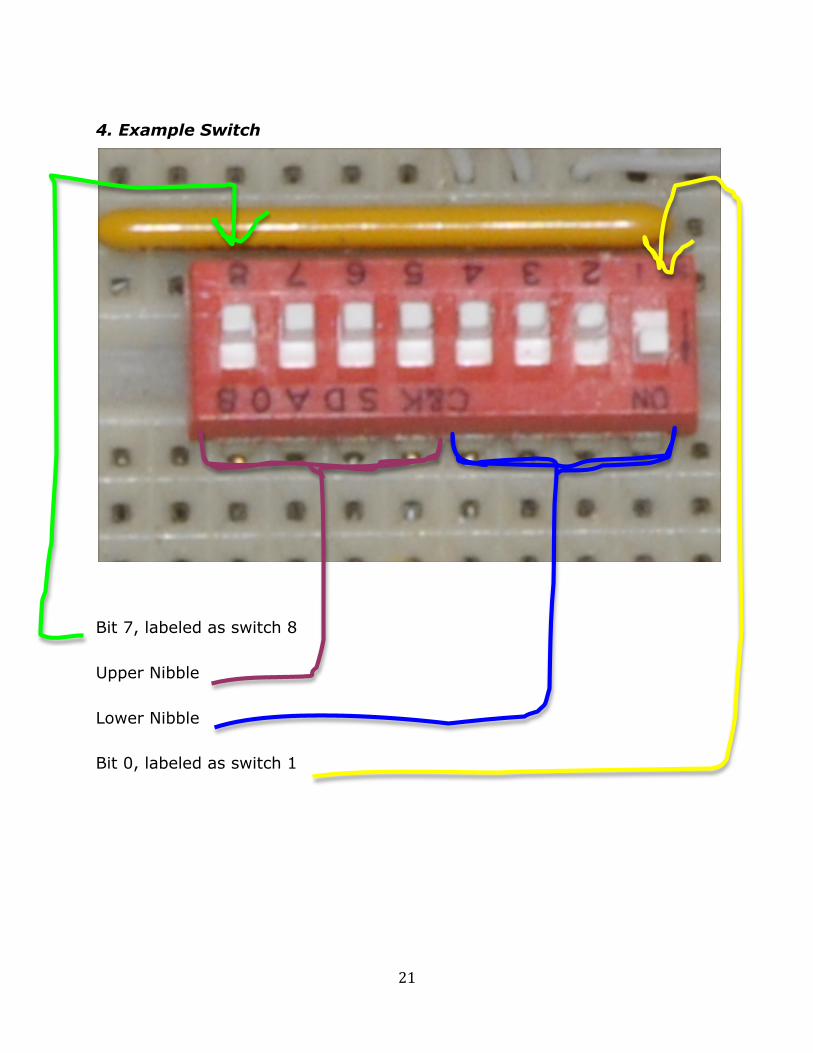
• Nibble—a 4-bit number; often, as in the case here, a nibble refers
to a hexadecimal digit.
o Upper Nibble: In a 2-digit hexadecimal number, the left digit
is the upper nibble
o Lower Nibble: In a 2-digit hexadecimal number, the right digit
is the lower nibble
o e.g. In the hexadecimal number “1f” the “1” is the upper
nibble and the “f” is the lower nibble.
o The hexadecimal number “1” can be represented by the
nibble “0001” and the hexadecimal number “f” can be
represented by the nibble “1111.” Hence, the hexadecimal
number “1f” can be represented on an 8-bit switch as the two
nibbles concatenated: “00011111”.
o See Photo 4

EDI Functional Test – Photos 3/23/11 1:38 PM
!)"
"
1. Overview Photo of Workbench
Test Source Power Supplies
Interface Breadboard
EDI Board
EDI Power Supplies

!*"
"
2. EDI Board
J1 26-pin Connector
J2 44-pin Connector
Potentiometer
“Jumper” Shorts
Big Rainbow Ribbon Cable to Interface Breadboard

#+"
"
3. Interface Breadboard
BAS – Board Address Switch (16 bits)
CS – Control Switch (8 bits)
IAES – Input Address Enable Switch (left-most bit, bit 7, on the CS)
(Note: it’s labeled as switch 8 on the CS)
RS – Read Switch (2nd from the right bit, bit 1, on CS)
(Note: it’s labeled as switch 2 on the CS)
WS – Write Switch
IAS – Input Address Switch (8 bits)
Lights (16 bits)
#!"
"
4. Example Switch
Bit 7, labeled as switch 8
Upper Nibble
Lower Nibble
Bit 0, labeled as switch 1

##"
"
5. CTSPS and VTSPS
VTSPS
CTSPS
Voltage Divider
VTSPS Multimeter
CTSPS Multimeter (not pictured)

#$"
"
6. J1 26-pin Connector
Red wire in pin 1
White wire in pin 10
Black wire in pin 19

#%"
"
7. Positioning the J1 Connector (a)

#&"
"
8. Positioning the J1 Connector (b)
Note: It is moved over ONE space!

#'"
"
9. J2 44-pin Connector
Red wire in pin 31
Black wire in pin 32
Blue wires in pins 1 and 16
Green wires in pins 2 and 17
Purple wires in pins 3 and 18

#("
"
10. Positioning the J2 Connector (a)

#)"
"
11. Positioning the J2 Connector (b)
Note: It is moved over TWO spaces!!!!!!

EDI Functional Test – Data Sheet 3/23/11 1:38 PM
#*"
"
EDI Revision and Serial Number: ____________________
Test Date: ____________________
Tested By: ____________________
Input HSV (measured) Pull-Up? Input HSV (measured)
V0 n/a I0
V1 n/a I1
V2 n/a I2
V3 n/a I3
V4 n/a I4
V5 n/a I5
V6 n/a I6
V7 n/a I7
V8 n/a
V9 n/a
V10 n/a
V11 n/a
T0
T1
T2
T3
T4
T5
T6
T7
T8
T9
T10
T11
T12
T13
T14
T15
Issues:


Related Documents