March 2017 DocID029451 Rev 2 1/56 This is information on a product in full production. www.st.com STWLC03 Dual mode Qi/PMA wireless power receiver Datasheet - production data Features 1 W to 12 W output power Qi 1.1 and PMA wireless standard communication protocols Integrated high efficiency synchronous rectifier 800 kHz programmable step-down converter with input current and input voltage regulation loops Step-down converter efficiency up to 90% Simplified Li-Ion/Polymer charger function 32-bit, 16 MHz embedded microcontroller with 16 kB ROM and 2 kB RAM memory 2 kB NVM for customization Integrated driver for external supply switch Precise voltage and current measurements for received power calculation I 2 C interface Configurable GPIO output Rx coil NTC protection Thermal protection Low power dissipative rectifier overvoltage clamp Flip Chip 77 bumps (3.12x4.73 mm) Applications Cellular phones Power banks Navigation systems Tablets Medical and healthcare instrumentation Description The STWLC03 is an integrated wireless power receiver solution suitable for portable applications. The STWLC03 is able to operate with Qi 1.1 or PMA communication protocol. Thanks to the integrated low impedance synchronous rectifier and DC-DC step-down converter, the STWLC03 achieves high efficiency, low power dissipation and output power beyond 5 W. Digital control and precise analog control loops ensure stable operation. I 2 C interface allows many parameters to be customized in the device and this configuration can be stored in the embedded NVM. The STWLC03 can deliver the output power in two modes: as a power supply with configured output voltage or as a simple CC/CV battery charger with configurable charging current. The STWLC03 can detect an external (wired) power supply connection and drive an external power switch. Table 1: Device summary Order code Description Package Packing STWLC03JR 12 W output Flip Chip 77 bumps (3.12x4.73 mm) Tape and reel

Welcome message from author
This document is posted to help you gain knowledge. Please leave a comment to let me know what you think about it! Share it to your friends and learn new things together.
Transcript

March 2017 DocID029451 Rev 2 1/56
This is information on a product in full production. www.st.com
STWLC03
Dual mode Qi/PMA wireless power receiver
Datasheet - production data
Features 1 W to 12 W output power
Qi 1.1 and PMA wireless standard communication protocols
Integrated high efficiency synchronous rectifier
800 kHz programmable step-down converter with input current and input voltage regulation loops
Step-down converter efficiency up to 90%
Simplified Li-Ion/Polymer charger function
32-bit, 16 MHz embedded microcontroller with 16 kB ROM and 2 kB RAM memory
2 kB NVM for customization
Integrated driver for external supply switch
Precise voltage and current measurements for received power calculation
I2C interface
Configurable GPIO output
Rx coil NTC protection
Thermal protection
Low power dissipative rectifier overvoltage clamp
Flip Chip 77 bumps (3.12x4.73 mm)
Applications Cellular phones
Power banks
Navigation systems
Tablets
Medical and healthcare instrumentation
Description The STWLC03 is an integrated wireless power receiver solution suitable for portable applications. The STWLC03 is able to operate with Qi 1.1 or PMA communication protocol. Thanks to the integrated low impedance synchronous rectifier and DC-DC step-down converter, the STWLC03 achieves high efficiency, low power dissipation and output power beyond 5 W. Digital control and precise analog control loops ensure stable operation. I2C interface allows many parameters to be customized in the device and this configuration can be stored in the embedded NVM.
The STWLC03 can deliver the output power in two modes: as a power supply with configured output voltage or as a simple CC/CV battery charger with configurable charging current.
The STWLC03 can detect an external (wired) power supply connection and drive an external power switch.
Table 1: Device summary
Order code Description Package Packing
STWLC03JR 12 W output Flip Chip 77 bumps (3.12x4.73 mm) Tape and reel
Contents STWLC03
2/56 DocID029451 Rev 2
Contents
1 Introduction ..................................................................................... 6
2 Pin configuration ............................................................................. 7
3 Maximum ratings ........................................................................... 10
4 Electrical characteristics .............................................................. 12
5 Device description ......................................................................... 17
5.1 Using the STWLC03 as a power supply .......................................... 17
5.2 Using the STWLC03 as a battery charger ....................................... 17
5.3 Wireless standard auto-detection .................................................... 18
5.4 Qi operation and flow chart ............................................................. 19
5.4.1 Received power calibration (FOD feature) ....................................... 21
5.5 PMA operation ................................................................................ 21
5.6 External power supply ..................................................................... 22
5.7 The device interface ........................................................................ 24
6 I2C register description ................................................................. 25
6.1 ADC measured values .................................................................... 31
6.2 Service registers ............................................................................. 33
7 Non-volatile memory ..................................................................... 35
7.1 NVM sector maps ............................................................................ 35
8 Application information ................................................................ 45
8.1 Application schematic and recommended external components..... 45
8.2 External passive component selection ............................................ 49
8.2.1 Input resonant circuit component selection (L1, C1, C2) ................. 49
8.2.2 Voltage clamp resistor selection (RCL1, RCL2) ............................... 49
8.2.3 Load modulation capacitors selection (CM1, CM2) ......................... 49
8.2.4 Feedback resistor divider components selection (RFB1, RFB2) ..... 49
8.2.5 Rx NTC circuit component selection (RNTC, R1) ............................ 49
8.2.6 Soft-start capacitor selection (C10) .................................................. 50
8.2.7 External supply transistor selection .................................................. 50
8.3 Reference PCB layout ..................................................................... 51
9 Package information ..................................................................... 53
9.1 Flip Chip 77 bumps (3.12x4.73 mm) package information .............. 53
10 Revision history ............................................................................ 55
STWLC03 List of tables
DocID029451 Rev 2 3/56
List of tables
Table 1: Device summary ........................................................................................................................... 1 Table 2: Pin description .............................................................................................................................. 7 Table 3: Absolute maximum ratings ......................................................................................................... 10 Table 4: Thermal data ............................................................................................................................... 11 Table 5: Electrical characteristics ............................................................................................................. 12 Table 6: Recommended VRECT and VRMIN values for various VOUT .................................................. 17 Table 7: EPT reasons in Qi ....................................................................................................................... 20 Table 8: EOC reasons in PMA .................................................................................................................. 22 Table 9: User register map ....................................................................................................................... 25 Table 10: Control register ......................................................................................................................... 25 Table 11: Target rectified voltage register (register address 02h) ............................................................ 26 Table 12: Input voltage threshold for output power limitation register (register address 03h) ................. 26 Table 13: Input current limit register (register address 05h) ..................................................................... 26 Table 14: Overload threshold register (register address 06h) .................................................................. 26 Table 15: Step-down output voltage register (register address 07h) ....................................................... 27 Table 16: Step-down converter feedback voltages .................................................................................. 27 Table 17: Buck current limit register ......................................................................................................... 27 Table 18: Chip overtemperature threshold register (register address 09h) .............................................. 27 Table 19: Interrupt mask L register (register address 0Ah) ...................................................................... 27 Table 20: Interrupt mask H register ( register address 0Bh) .................................................................... 28 Table 21: Interrupt status L register ( register address 0Ch) .................................................................... 28 Table 22: Interrupt status H register ......................................................................................................... 29 Table 23: Interrupt latch L register ............................................................................................................ 29 Table 24: Interrupt latch H register ........................................................................................................... 29 Table 25: Operation mode detection status register ................................................................................. 30 Table 26: Operation mode detection control register (register address 11h) ........................................... 30 Table 27: Qi charge status register (register address 12h) ...................................................................... 31 Table 28: Charger status register (register address 13h) ......................................................................... 31 Table 29: Charger control register ............................................................................................................ 31 Table 30: ADC measured value register map .......................................................................................... 31 Table 31: Rectified voltage (VRECT) ........................................................................................................ 32 Table 32: Rectified output current (IRECT) .............................................................................................. 32 Table 33: RX coil NTC voltage ................................................................................................................. 32 Table 34: VOUT voltage ........................................................................................................................... 32 Table 35: VDROP voltage ........................................................................................................................ 33 Table 36: Chip temperature ...................................................................................................................... 33 Table 37: Ground voltage ......................................................................................................................... 33 Table 38: RX_POWER ............................................................................................................................. 33 Table 39: Service register map ................................................................................................................. 34 Table 40: NVM control .............................................................................................................................. 34 Table 41: I2C registers corresponding to bytes in NVM sector ................................................................ 34 Table 42: Non-volatile memory sector map .............................................................................................. 35 Table 43: Map of NVM sector 04 .............................................................................................................. 35 Table 44: Byte 0 ........................................................................................................................................ 36 Table 45: Byte 1 ........................................................................................................................................ 36 Table 46: Byte 2 ........................................................................................................................................ 36 Table 47: Byte 3 ........................................................................................................................................ 36 Table 48: Byte 4 ........................................................................................................................................ 37 Table 49: Map of NVM sector 05 .............................................................................................................. 37 Table 50: Map of NVM sector 07 .............................................................................................................. 38 Table 51: Map of NVM sector 08 .............................................................................................................. 39 Table 52: Map of NVM sector 10 .............................................................................................................. 40 Table 53: Map of NVM sector 13 .............................................................................................................. 41

List of tables STWLC03
4/56 DocID029451 Rev 2
Table 54: Byte 0 Qi_EPT_threshold [7:0] ................................................................................................. 41 Table 55: Byte 1, Qi_EPT_Time [7:0] ....................................................................................................... 41 Table 56: Byte 2, Qi charger enable ......................................................................................................... 42 Table 57: Qi target voltage ....................................................................................................................... 42 Table 58: Byte 3, Q1_Precharge_Battery_overvoltage ............................................................................ 42 Table 59: Byte 4, Q1_Precharge and Fastcharge .................................................................................... 42 Table 60: Byte 8, PMA_EOC_theshold [7:0] ............................................................................................ 43 Table 61: Byte 9, PMA_EOC_Time [7:0] .................................................................................................. 43 Table 62: Byte 10, PMA_Target_Voltage [2:0] ......................................................................................... 43 Table 63: PMA target voltage vs charging voltage ................................................................................... 44 Table 64: Byte 11 ...................................................................................................................................... 44 Table 65: Byte 12 ...................................................................................................................................... 44 Table 66: STWLC03 recommended external components....................................................................... 46 Table 67: Flip Chip 77 bumps (3.12x4.73 mm) package mechanical data .............................................. 54 Table 68: Document revision history ........................................................................................................ 55

STWLC03 List of figures
DocID029451 Rev 2 5/56
List of figures
Figure 1: Simplified block diagram .............................................................................................................. 6 Figure 2: Pin configuration Flip Chip 77 bumps (3.12x4.73 mm) ............................................................... 7 Figure 3: Typical step-down converter efficiency ..................................................................................... 17 Figure 4: Typical charging profile .............................................................................................................. 18 Figure 5: Wireless standard detection flowchart ....................................................................................... 19 Figure 6: Qi simplified flow diagram .......................................................................................................... 20 Figure 7: PMA simplified flow diagram ..................................................................................................... 21 Figure 8: External power supply situation ................................................................................................. 23 Figure 9: External power supply situation 1 .............................................................................................. 23 Figure 10: STWLC03 application schematic ............................................................................................ 45 Figure 11: STWLC03 charger configuration ............................................................................................. 46 Figure 12: VIO and digital interface in standalone application schematic ................................................ 48 Figure 13: VIO and digital interface in platform application schematic ..................................................... 48 Figure 14: Top overlay .............................................................................................................................. 51 Figure 15: Top layer .................................................................................................................................. 51 Figure 16: Mid layer 1 ............................................................................................................................... 51 Figure 17: Mid layer 2 ............................................................................................................................... 51 Figure 18: Bottom layer............................................................................................................................. 52 Figure 19: Flip Chip 77 bumps (3.12x4.73 mm) package outline ............................................................. 53 Figure 20: Flip Chip 77 bumps (3.12x4.73 mm) recommended footprint ................................................. 54

Introduction STWLC03
6/56 DocID029451 Rev 2
1 Introduction
The STWLC03 is a dual mode Qi/PMA wireless power receiver. It works as a voltage source with regulated output voltage, typically 5 V. It can be reconfigured into a simple battery charger mode (CC/CV) to charge directly Li-Ion or Li-Pol batteries. The STWLC03 can operate autonomously or can be controlled through I2C by the host system.
Figure 1: Simplified block diagram

STWLC03 Pin configuration
DocID029451 Rev 2 7/56
2 Pin configuration Figure 2: Pin configuration Flip Chip 77 bumps (3.12x4.73 mm)
Table 2: Pin description
Pin name Pin position Description
AC1 F6, F7, G7 RX coil circuit terminal connection
AC2 E9, E10, E11 RX coil circuit terminal connection
MOD1 G6 Load modulation capacitor 1 connection
MOD2 F11 Load modulation capacitor 2 connection
CLMP1 G5 Clamping capacitor/resistor 1 connection
CLMP2 F9 Clamping capacitor/resistor 2 connection
RMOD E7 Modulation current sink connection, internally connected to VRECT
RMOD1 G11 Load modulation external resistor connection.
RM resistor is not necessary for most applications
VRECT F10, G10 Synchronous rectifier output
BOOT1 G8 Bootstrap capacitor connection for the rectifier
BOOT2 E8 Bootstrap capacitor connection for the rectifier
BOOT G9 Bootstrap capacitor connection for the step-down converter
CLAMP F8 Low power clamp connection
VSUP A8, B8, B7 Power supply input for the step-down converter
VSUPS A7, C6 Sensing terminal of the external current sensing resistor
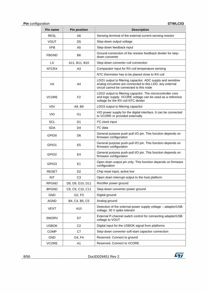
Pin configuration STWLC03
8/56 DocID029451 Rev 2
Pin name Pin position Description
RESL A6 Sensing terminal of the external current sensing resistor
VOUT D5 Step-down output voltage
VFB A5 Step-down feedback input
FBGND B6 Ground connection of the resistor feedback divider for step-down converter
LX A11, B11, B10 Step-down converter coil connection
NTCRX A3 Comparator input for RX coil temperature sensing
NTC thermistor has to be placed close to RX coil
VA A4
LDO1 output to filtering capacitor. ADC supply and sensitive analog circuitries are connected to this LDO; any external circuit cannot be connected to this node
VCORE F2
LDO2 output to filtering capacitor. The microcontroller core and logic supply. VCORE voltage can be used as a reference voltage for the RX coil NTC divider
V5V A9, B9 LDO3 output to filtering capacitor
VIO G1 VIO power supply for the digital interface. It can be connected to VCORE or provided externally
SCL D1 I2C clock input
SDA D4 I2C data
GPIO0 D6 General purpose push-pull I/O pin. This function depends on firmware configuration
GPIO1 E5 General purpose push-pull I/O pin. This function depends on firmware configuration
GPIO2 E4 General purpose push-pull I/O pin. This function depends on firmware configuration
GPIO3 E1 Open drain output pin only. This function depends on firmware configuration
RESET D2 Chip reset input, active low
INT C3 Open drain interrupt output to the host platform
RPGND D8, D9, D10, D11 Rectifier power ground
BPGND C8, C9, C10, C11 Step-down converter power ground
GND G2, F3 Digital ground
AGND B4, C4, B5, C5 Analog ground
VEXT A10 Detection of the external power supply voltage – adapter/USB voltage. 30 V spike tolerant
SWDRV D7 External P-channel switch control for connecting adapter/USB voltage to VOUT
USBOK C2 Digital input for the USBOK signal from platforms
COMP C7 Step-down converter soft-start capacitor connection
GND G4, F4 Reserved. Connect to ground
VCORE A1 Reserved. Connect to VCORE
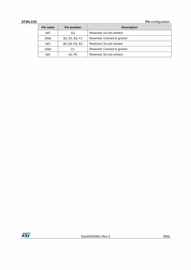
STWLC03 Pin configuration
DocID029451 Rev 2 9/56
Pin name Pin position Description
N/C G3 Reserved. Do not connect
GND B1, E2, E6, F1 Reserved. Connect to ground
N/C B2, B3, D3, E3 Reserved. Do not connect
GND C1 Reserved. Connect to ground
N/C A2, F5 Reserved. Do not connect
Maximum ratings STWLC03
10/56 DocID029451 Rev 2
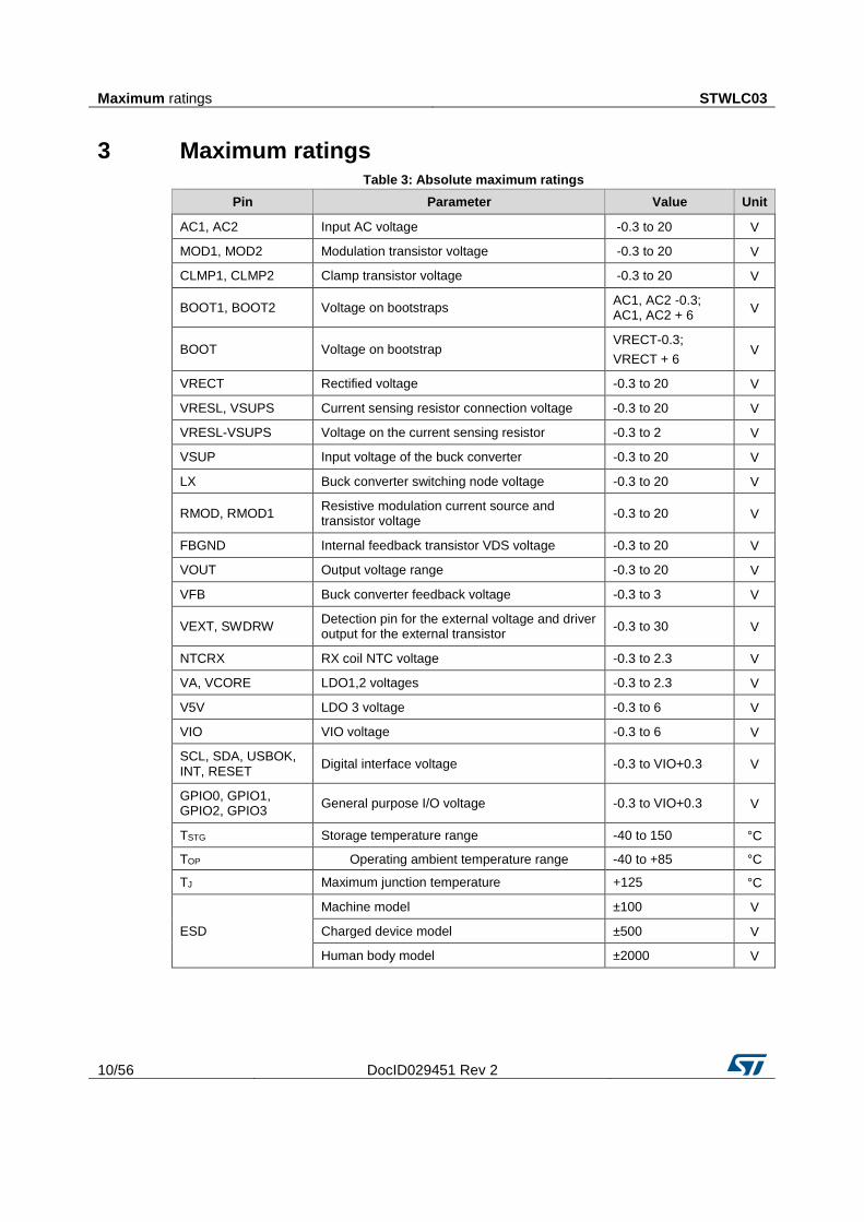
3 Maximum ratings Table 3: Absolute maximum ratings
Pin Parameter Value Unit
AC1, AC2 Input AC voltage -0.3 to 20 V
MOD1, MOD2 Modulation transistor voltage -0.3 to 20 V
CLMP1, CLMP2 Clamp transistor voltage -0.3 to 20 V
BOOT1, BOOT2 Voltage on bootstraps AC1, AC2 -0.3; AC1, AC2 + 6
V
BOOT Voltage on bootstrap VRECT-0.3;
VRECT + 6 V
VRECT Rectified voltage -0.3 to 20 V
VRESL, VSUPS Current sensing resistor connection voltage -0.3 to 20 V
VRESL-VSUPS Voltage on the current sensing resistor -0.3 to 2 V
VSUP Input voltage of the buck converter -0.3 to 20 V
LX Buck converter switching node voltage -0.3 to 20 V
RMOD, RMOD1 Resistive modulation current source and transistor voltage
-0.3 to 20 V
FBGND Internal feedback transistor VDS voltage -0.3 to 20 V
VOUT Output voltage range -0.3 to 20 V
VFB Buck converter feedback voltage -0.3 to 3 V
VEXT, SWDRW Detection pin for the external voltage and driver output for the external transistor
-0.3 to 30 V
NTCRX RX coil NTC voltage -0.3 to 2.3 V
VA, VCORE LDO1,2 voltages -0.3 to 2.3 V
V5V LDO 3 voltage -0.3 to 6 V
VIO VIO voltage -0.3 to 6 V
SCL, SDA, USBOK, INT, RESET
Digital interface voltage -0.3 to VIO+0.3 V
GPIO0, GPIO1, GPIO2, GPIO3
General purpose I/O voltage -0.3 to VIO+0.3 V
TSTG Storage temperature range -40 to 150 °C
TOP Operating ambient temperature range -40 to +85 °C
TJ Maximum junction temperature +125 °C
ESD
Machine model ±100 V
Charged device model ±500 V
Human body model ±2000 V

STWLC03 Maximum ratings
DocID029451 Rev 2 11/56
Absolute maximum ratings are those values beyond which damage to the device may occur. Functional operation under these conditions is not implied.
Table 4: Thermal data
Package Symbol Parameter Value Unit
Flip Chip 77 (3.12x4.73 mm) RTHJA Junction-to-ambient thermal resistance(1) 35 °C/W
Notes:
(1)This parameter corresponds to the PCB board, 4-layer with 1 inch2 of cooling area.

Electrical characteristics STWLC03
12/56 DocID029451 Rev 2
4 Electrical characteristics
-30 °C < TA < 85 °C; typical values are at TA = 25 °C, unless otherwise specified.
Table 5: Electrical characteristics
Symbol Parameter Test conditions Min. Typ. Max. Unit
General section
VIN AC input voltage
Peak-to-peak voltage between AC1- AC2 over the period
32 V
VUVLO Undervoltage lockout threshold
VSUP rising
3.6 3.8 V
VSUP falling 3.3 3.5
TIMEOUTRESET Reset time-out for shutdown mode
1
ms
IQ
Current consumption in the shutdown mode
RESET=0 (active low) duration>1 ms, measured at VEXT
10
μA
RESET=0 (active low) duration>1 ms, measured at VRECT
2 4 mA
IRESET
Current consumption in the RESET condition
RESET=0 (active low), duration<1 ms, GPIO 0 floating
5
mA
ICC Current consumption of the device
RESET=1 (inactive), GPIO 0 floating
7
mA
LDO 1
VA LDO 1 output voltage
IA = 5 mA
1.8
V
IILIM Load current limit
50
mA
LDO 2
VCORE LDO 2 output voltage
VSUP = 3.6 V to
11 V, ICORE = 5 mA
1.8
V
IDDLIM Load current limit
40
mA
LDO 3
V5V LDO 3 output voltage
IV5V = 20 mA,
VR = 5.5 V 5
V
IILIM Load current limit
30
mA
Synchronous rectifier

STWLC03 Electrical characteristics
DocID029451 Rev 2 13/56
Symbol Parameter Test conditions Min. Typ. Max. Unit
RDS(on)
Drain-source NMOS on- resistance low-side
IRECT = 1.4 A,
VRECT = 8 V 90
mΩ Drain-source NMOS on-resistance high-side
70
Efficiency Rectifier efficiency
IRECT = 0.8 A, VRECT = 7 V,
fRectifier = 130 kHz
91
%
IRACTIVE Active mode rectifier threshold, voltage @ Rs
VRECT = 10 V, rising edge
8.75
mV VRECT = 10 V, falling edge
3.25
fRECTIFIER Rectifier frequency range
50
500 kHz
VCLAMP Clamp of the rectified voltage
ICLAMP = 1 mA
17.4
V
Active clamp drivers
RDS(on)CLMP1,2 Active clamp MOS RDS(on)
VSUP = 5 V
1
Ω
VOVP VRECT voltage threshold of active clamp
15.4 15.9 16.4 V
VOVP hyst VRECT voltage active clamp hysteresis
600
mV
Load modulation
RDS(on)MOD1,2 Load modulation MOS RDS(on)
VSUP = 5 V
1
Ω
IMOD
RMOD pin sink current range
VSUP = 5 V 15
410 mA
Modulation current tolerance
VSUP = 5 to 12 V, IMOD = 80 mA
10
%
IMAXMOD1
VSUP = 5 V,
RM = 2 Ω 2
A
Protections
VLDMAX.
Overcurrent protection threshold, voltage @ RS
VLDMAX = 0Fh
1.7 V
VLDMAX = 04h
0.875
TOL_VLDMAX
Tolerance of the VLDMAX
VLDMAX = 0Fh -5
+5 %
VLDMAX = 04h
-10
+10

Electrical characteristics STWLC03
14/56 DocID029451 Rev 2
Symbol Parameter Test conditions Min. Typ. Max. Unit
VNTCTRIG NTC trigger voltage for RX
0.6
V
TOL_VNTCTRIG NTC trigger voltage tolerance
3
%
Hyst_VNTCTRIG NTC trigger voltage hysteresis
100
mV
tSHDN Thermal shutdown
150
°C
tSHDNHYST Thermal shutdown hysteresis
20
°C
Current-to-voltage converter
EOC_CURRENT End-of-charge current threshold
RS = 0.05 Ω 1%, VSUP = 5 to 15 V
0
400 mA
TOLEOC_CURRENT Tolerance of the EOC threshold
RS = 0.05 Ω 1%, VSUP = 5 to 15 V, EOC_CURRENT = 50 mA
20
%
RS = 0.05 Ω 1%, VSUP = 5 to 15 V, EOC_CURRENT = 200 mA
10
%
Step-down converter
VVOUT Output voltage range
3
7 V
TolVOUT VOUT tolerance VOUTreg = 011, VOUT = 4.2 V
0.5
%
OVPVOUT Overvoltage protection threshold
8.5
V
IVOUT + IFB Output leakage current
Step-down is off, VOUT = 5 V,
1 µA
IFB Feedback pin bias current
500 nA
ILIM
Coil current limit
250
4000 mA
Coil current limit accuracy
CURRLIM reg = 1111
10
%
IOVERCURR Overcurrent/short-circuit protection
VSUP = 5 to 12 V
4500
mA
DIVVOUT Output voltage internal divider ratio
6
nA
fSW Switching frequency
0.8
MHz
VSUP Input voltage range
IOUT = 2 A 5.5
12 V
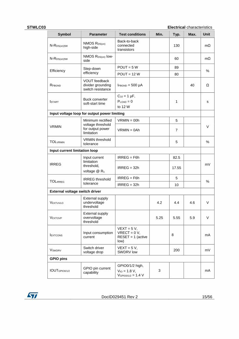
STWLC03 Electrical characteristics
DocID029451 Rev 2 15/56
Symbol Parameter Test conditions Min. Typ. Max. Unit
N-RDS(on)SW NMOS RDS(on) high-side
Back-to-back connected transistors
130
mΩ
N-RDS(on)SW NMOS RDS(on) low-side
60
mΩ
Efficiency Step-down efficiency
POUT = 5 W
89 %
POUT = 12 W
80
RFBGND VOUT feedback divider grounding switch resistance
IFBGND = 500 µA
40 Ω
tSTART Buck converter soft-start time
C10 = 1 µF,
PLOAD = 0
to 12 W
1
s
Input voltage loop for output power limiting
VRMIN
Minimum rectified voltage threshold for output power limitation
VRMIN = 00h
5
V VRMIN = 0Ah
7
TOLVRMIN VRMIN threshold tolerance
5
%
Input current limitation loop
IRREG
Input current limitation threshold,
voltage @ Rs
IRREG = F6h
82.5
mV IRREG = 32h
17.55
TOLIRREG IRREG threshold tolerance
IRREG = F6h
5 %
IRREG = 32h
10
External voltage switch driver
VEXTUVLO External supply undervoltage threshold
4.2 4.4 4.6 V
VEXTOVP External supply overvoltage threshold
5.25 5.55 5.9 V
IEXTCONS Input consumption current
VEXT = 5 V, VRECT = 0 V, RESET = 1 (active low)
8
mA
VSWDRV Switch driver voltage drop
VEXT = 5 V, SWDRV low
200
mV
GPIO pins
IOUTGPIO0/1/2 GPIO pin current capability
GPIO0/1/2 high,
VIO = 1.8 V, VGPIO0/1/2 = 1.4 V
3
mA

Electrical characteristics STWLC03
16/56 DocID029451 Rev 2
Symbol Parameter Test conditions Min. Typ. Max. Unit
VGPIO0/1/2/3 GPIO pin drop
GPIO0/1/2/3 low, VIO = 1.8 V,
IGPIO0/1/2 = 3 mA
360
mV
VIL Low level input voltage
0.3*VIO V
VIH High level input voltage
0.7*VIO
V
Microcontroller
Architecture
32
bit
NVM Memory size for customization
2
kbit
Clock generator
fOSC Clock generator frequency
VSUP = 4.5
to 15 V 16
MHz
TOLFOSC Tolerance of the clock generator frequency
TAMB = 0 °C
to 85 °C -4
+4 %
STWLC03 Device description
DocID029451 Rev 2 17/56
5 Device description
5.1 Using the STWLC03 as a power supply
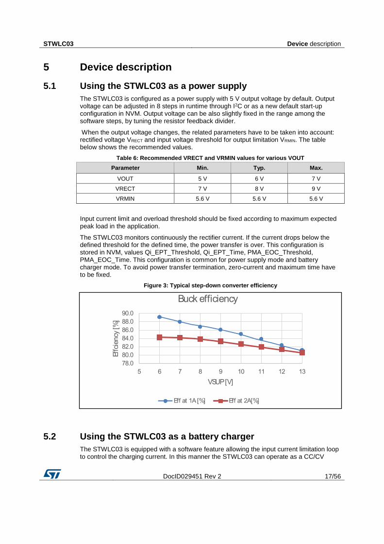
The STWLC03 is configured as a power supply with 5 V output voltage by default. Output voltage can be adjusted in 8 steps in runtime through I2C or as a new default start-up configuration in NVM. Output voltage can be also slightly fixed in the range among the software steps, by tuning the resistor feedback divider.
When the output voltage changes, the related parameters have to be taken into account: rectified voltage VRECT and input voltage threshold for output limitation VRMIN. The table below shows the recommended values.
Table 6: Recommended VRECT and VRMIN values for various VOUT
Parameter Min. Typ. Max.
VOUT 5 V 6 V 7 V
VRECT 7 V 8 V 9 V
VRMIN 5.6 V 5.6 V 5.6 V
Input current limit and overload threshold should be fixed according to maximum expected peak load in the application.
The STWLC03 monitors continuously the rectifier current. If the current drops below the defined threshold for the defined time, the power transfer is over. This configuration is stored in NVM, values Qi_EPT_Threshold, Qi_EPT_Time, PMA_EOC_Threshold, PMA_EOC_Time. This configuration is common for power supply mode and battery charger mode. To avoid power transfer termination, zero-current and maximum time have to be fixed.
Figure 3: Typical step-down converter efficiency
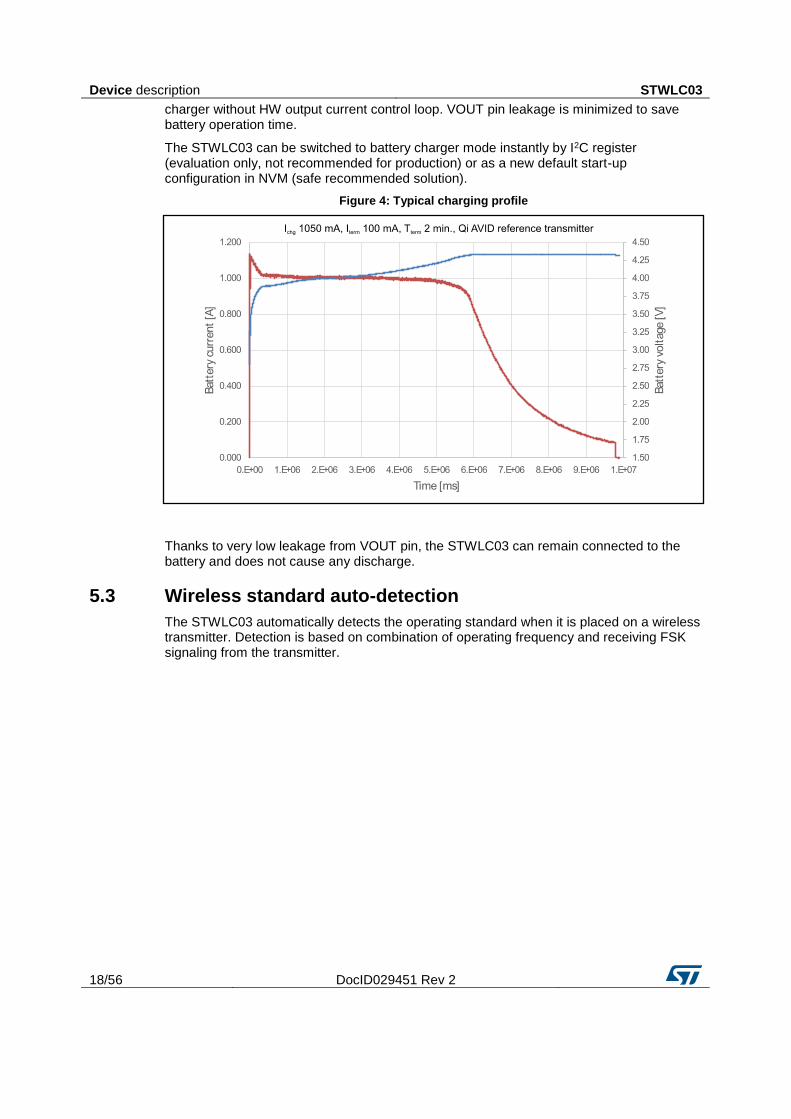
5.2 Using the STWLC03 as a battery charger
The STWLC03 is equipped with a software feature allowing the input current limitation loop to control the charging current. In this manner the STWLC03 can operate as a CC/CV
Device description STWLC03
18/56 DocID029451 Rev 2
charger without HW output current control loop. VOUT pin leakage is minimized to save battery operation time.
The STWLC03 can be switched to battery charger mode instantly by I2C register (evaluation only, not recommended for production) or as a new default start-up configuration in NVM (safe recommended solution).
Figure 4: Typical charging profile
Thanks to very low leakage from VOUT pin, the STWLC03 can remain connected to the battery and does not cause any discharge.
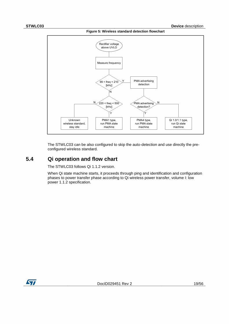
5.3 Wireless standard auto-detection
The STWLC03 automatically detects the operating standard when it is placed on a wireless transmitter. Detection is based on combination of operating frequency and receiving FSK signaling from the transmitter.
STWLC03 Device description
DocID029451 Rev 2 19/56
Figure 5: Wireless standard detection flowchart
The STWLC03 can be also configured to skip the auto-detection and use directly the pre-configured wireless standard.
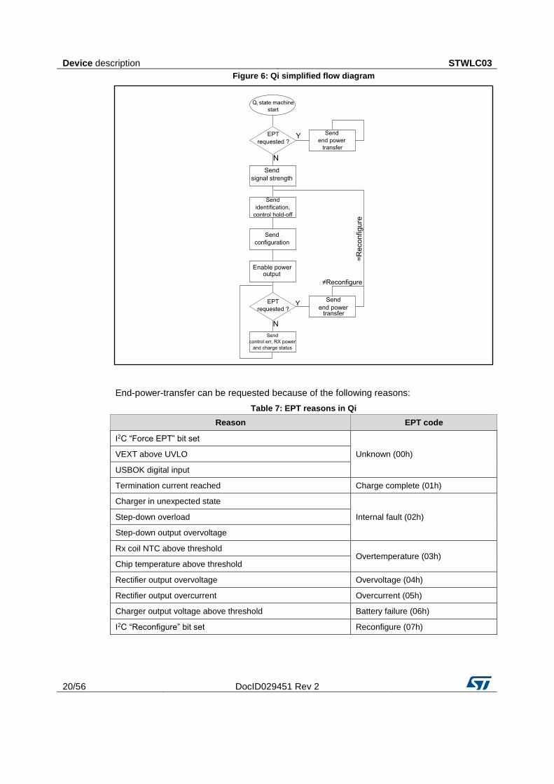
5.4 Qi operation and flow chart
The STWLC03 follows Qi 1.1.2 version.
When Qi state machine starts, it proceeds through ping and identification and configuration phases to power transfer phase according to Qi wireless power transfer, volume I: low power 1.1.2 specification.
Device description STWLC03
20/56 DocID029451 Rev 2
Figure 6: Qi simplified flow diagram
End-power-transfer can be requested because of the following reasons:
Table 7: EPT reasons in Qi
Reason EPT code
I2C “Force EPT” bit set
Unknown (00h) VEXT above UVLO
USBOK digital input
Termination current reached Charge complete (01h)
Charger in unexpected state
Internal fault (02h) Step-down overload
Step-down output overvoltage
Rx coil NTC above threshold Overtemperature (03h)
Chip temperature above threshold
Rectifier output overvoltage Overvoltage (04h)
Rectifier output overcurrent Overcurrent (05h)
Charger output voltage above threshold Battery failure (06h)
I2C “Reconfigure” bit set Reconfigure (07h)

STWLC03 Device description
DocID029451 Rev 2 21/56
5.4.1 Received power calibration (FOD feature)
Although the STWLC03 is well-trimmed, inaccuracy in the received power estimation can be caused in the target application due to manufacturing different environment conditions. Different serial resistances of used receiver coil or different shieldings of the receiver coil (e.g. battery or ground plane in a near proximity of the coil) are the main issues. The STWLC03 features dedicated adjustment options placed in NVM.
5.5 PMA operation
The STWLC03 follows PMA1 SR1 specification. When PMA state machine starts, it proceeds through ping and identification phase to power transfer phase according to PMA inductive wireless power and charging receiver specifications, system release 1.
Figure 7: PMA simplified flow diagram
End-of-charge can be requested due to the following reasons:
Device description STWLC03
22/56 DocID029451 Rev 2
Table 8: EOC reasons in PMA
Reasons
I2C “Force EOC” bit set
VEXT above UVLO
USBOK digital input
Termination current reached
Charger in unexpected state
Step-down overload
Step-down output overvoltage
Rx coil NTC above threshold
Chip temperature above threshold
Rectifier output overvoltage
Rectifier output overcurrent
Charger output voltage above threshold
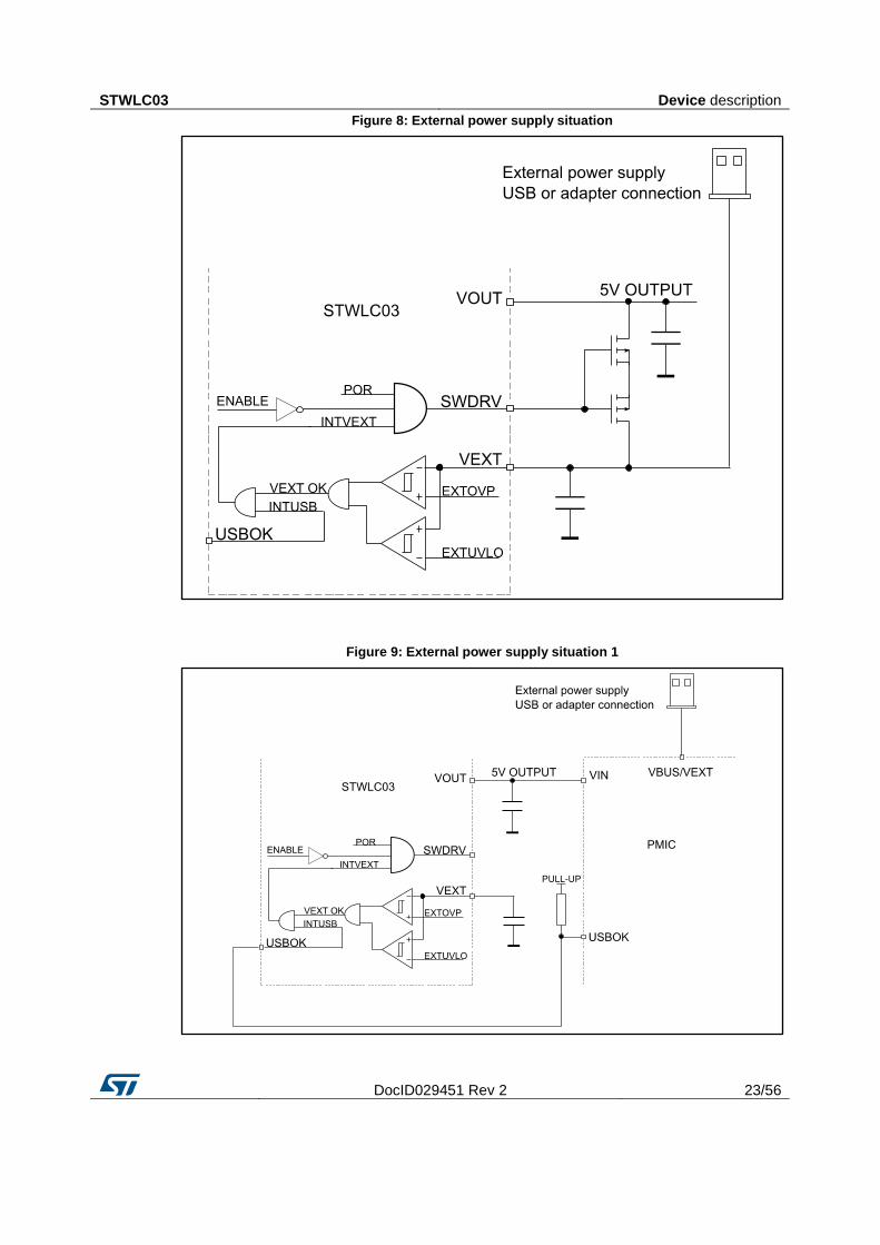
5.6 External power supply
Figure 8: "External power supply situation" illustrates the situation where the STWLC03 detects the external voltage presence and drives SWDRV (external voltage) to the output. The STWLC03 also terminates the wireless power transfer.
Figure 9: "External power supply situation 1" illustrates the situation where the STWLC03 is assembled in a system with another PMIC that serves multiple power supply inputs. PMIC uses digital line to let the STWLC03 know that there is a higher priority power supply available and the wireless power transfer should be terminated.
For proper operation, RESETn pin must be high. Connecting VEXT power supply, consumption from VIO increases if VIO supply is provided externally. (It has not effect if VIO is connected to VCORE).
STWLC03 Device description
DocID029451 Rev 2 23/56
Figure 8: External power supply situation
Figure 9: External power supply situation 1
Device description STWLC03
24/56 DocID029451 Rev 2
5.7 The device interface
The STWLC03 is equipped with I2C interface with an open-drain interrupt line to connect with the host system. If I2C connection is not used by the host platform, SDA and SCL lines should be pulled-up to VIO voltage. The STWLC03 contains RESETn input. The device under reset conditions has very low power consumption. If reset is not controlled by the host platform it should be pulled-up to VIO voltage. USBOK is a digital input, which terminates power transfer if another preferred power supply is available. The STWLC03 features GPIO pins. By default GPIO 0 only is active and detects power transfer state on wireless interface.
STWLC03 I2C register description
DocID029451 Rev 2 25/56
6 I2C register description
The device I2C address is 14h (0010100b).
Table 9: User register map
Address Register
00h Control
01h Reserved
02h Target rectified voltage
03h Input voltage threshold for output limitation
04h Reserved
05h Input current limit
06h Overload threshold
07h Buck output voltage
08h Buck current limit
09h Chip overtemperature
0Ah Interrupt mask L
0Bh Interrupt mask H
0Ch Interrupt status L
0Dh Interrupt status H
0Eh Interrupt latch L
0Fh Interrupt latch H
10h Operation mode detection status
11h Operation mode detection control
12h Qi charge status packet content
13h Charger status
14h Charger control
Table 10: Control register
b7 b6 b5 b4 b3 b2 b1 b0
Force/EPT Disable/EPT on error Qi reconfigure - - - - USBcon_cnf R/W
Loaded from NVM at startup Default
USBcon_cnf:
0: auto connect switch + disable buck + send EPT@VEXT/disable buck + send EPT@USBOK
1: ignore VEXT/USBOK completely
Qi reconfigure:
0: no action

I2C register description STWLC03
26/56 DocID029451 Rev 2
1: send reconfigure packet (auto-clear)
Disable EPT on error:
0: automatically send EPT to OVP, overload, overtemperature or buck fault
1: do not send EPT automatically, wait for master
Force EPT:
0: no action
1: send EPT (auto-clear)
Table 11: Target rectified voltage register (register address 02h)
b7 b6 b5 b4 b3 b2 b1 b0
TARGET_VRECT[7:0] R/W
Loaded from NVM at startup Default
The target rectifier output voltage.
Rectified voltage = 0.25 V * TARGET_VRECT
Valid range 14h - 30h (5 V - 12 V).
Table 12: Input voltage threshold for output power limitation register (register address 03h)
b7 b6 b5 b4 b3 b2 b1 b0
- - VRMIN[5:0] R/W
Loaded from NVM at startup Default
VRMIN represents a VRECT voltage threshold where step-down converter applies output power limitation to prevent VRECT from dropping too low.
Threshold = 5.0 V + VRMIN * 0.2 V
Valid range from 00h to 0Ah (5.0 V – 7 V). Recommended value is 01h (5.2 V).
Table 13: Input current limit register (register address 05h)
b7 b6 b5 b4 b3 b2 b1 b0
INPUT_CURR_LIMIT[7:0] R/W
Loaded from NVM at startup Default
Output power does not exceed this input current limit. The current is sensed on the sensing resistor (RS).
Input current limit = (1.625 mV + INPUT_CURR_LIMIT * 0.325 mV) / RS.
Valid range from 00h to F6h (0.001625 V – 0.0816 V ~ 16.25 mA – 816 mA @ 100 mΩ RS).
Table 14: Overload threshold register (register address 06h)
b7 b6 b5 b4 b3 b2 b1 b0
- - - - OVERLOAD_THRD[3:0] R/W
Loaded from NVM at startup Default
This register configures overcurrent protection threshold, sensed on the sensing resistor (RS). Voltage represents the voltage drop caused by current flowing through the sensing

STWLC03 I2C register description
DocID029451 Rev 2 27/56
resistor. Overcurrent protection threshold = (6.25 mV + OVERLOAD_THRD * 6.25 mV) / RS.
Valid range 00h – 0Fh (6.25 mV – 100 mV ~ 0.0625 A – 1 A @ 100 mΩ RS.
Table 15: Step-down output voltage register (register address 07h)
b7 b6 b5 b4 b3 b2 b1 b0
- - - - - STEP_DOWN_OUTPUT_VOLT[2:0] R/W
Loaded from NVM at startup Default
This register sets step-down converter feedback reference voltage. Output voltage is derived from the feedback voltage through the feedback resistor divider.
Table below shows values of the reference voltage of the step-down converter for each setting and the VOUT voltage assuming the typical recommended feedback resistor divider.
Table 16: Step-down converter feedback voltages
BUCK_OUTPUT_VOLT STEP_DOWN FB REF [V] VOUT [V]
000 0.57 3.30
001 0.62 3.60
010 0.70 4.10
011 0.72 4.20
100 0.86 5.00
Table 17: Buck current limit register
b7 b6 b5 b4 b3 b2 b1 b0
- - - - BUCK_ILIM[3:0] R/W
Loaded from NVM at startup Default
This register sets the peak coil current limit value of the buck converter.
Peak current = 250 mA + BUCK_ILIM * 250 mA.
Valid range from 00h to 04h (250 mA – 1250 mA).
Table 18: Chip overtemperature threshold register (register address 09h)
b7 b6 b5 b4 b3 b2 b1 b0
CHIP_OVERTEMP_THRESHOLD[7:0] R/W
Loaded from NVM at startup Default
This threshold is compared to the value read by the AD converter from the chip temperature channel divided by 4.
Table 19: Interrupt mask L register (register address 0Ah)
b7 b6 b5 b4 b3 b2 b1 b0
INT_MASK_L R/W
Loaded from NVM at startup Default
Interrupt mask register ( INT output only is masked, no effect on EPT):

I2C register description STWLC03
28/56 DocID029451 Rev 2
b0: buck fault
b1: overload
b2: chip overtemperature
b3: coil overtemperature
b4: VRECT overvoltage
b5: VEXT (external voltage connection)
b6: USB OK (USB connection)
b7: standard detection finished
0 = interrupt not masked
1 = interrupt masked
Table 20: Interrupt mask H register ( register address 0Bh)
b7 b6 b5 b4 b3 b2 b1 b0
INT_MASK_H R/W
Loaded from NVM at startup Default
Interrupt mask register (INT output only is masked, no effect on EPT):
b0: charging finished
b1: charger internal fault
b2: charger battery fail
b3: not used
b4: not used
b5: not used
b6: not used
b7: not used
0 = interrupt not masked
1 = interrupt masked
Table 21: Interrupt status L register ( register address 0Ch)
b7 b6 b5 b4 b3 b2 b1 b0
INT_STATUS_L Read only
0 0 0 0 0 0 0 0 Default
b0: N/A
b1: N/A
b2: chip overtemperature
b3: coil overtemperature
b4: N/A
b5: VEXT (external voltage connection)
b6: USB OK (USB connection)

STWLC03 I2C register description
DocID029451 Rev 2 29/56
b7: standard detection finished
Bit value 1 means valid, 0 means not valid.
Table 22: Interrupt status H register
b7 b6 b5 b4 b3 b2 b1 b0
INT_STATUS_H Read only
1 0 0 0 0 0 0 0 Default
b0: charging finished
b1: charger internal fault
b2: charger battery fail
b3: N/A
b4: N/A
b5: N/A
b6: N/A
b7: N/A
Bit value 1 means valid, 0 means not valid.
Table 23: Interrupt latch L register
b7 b6 b5 b4 b3 b2 b1 b0
INT_LATCH_L Read/clear
0 0 0 0 0 0 0 0 Default
b0: buck fault
b1: overload
b2: chip overtemperature
b3: coil overtemperature
b4: VRECT overvoltage
b5: VEXT (external voltage connection)
b6: USB OK (USB connection)
b7: standard detection finished
Bit value 1 means valid, 0 means not valid.
Table 24: Interrupt latch H register
b7 b6 b5 b4 b3 b2 b1 b0
INT_LATCH_H Read/clear
0 0 0 0 0 0 0 0 Default
b0: charging finished
b1: charger internal fault
b2: charger battery fail
I2C register description STWLC03
30/56 DocID029451 Rev 2
b3: N/A
b4: N/A
b5: N/A
b6: N/A
b7: power ON in I2C driven standard detection mode
Bit value 1 means valid, 0 means not valid.
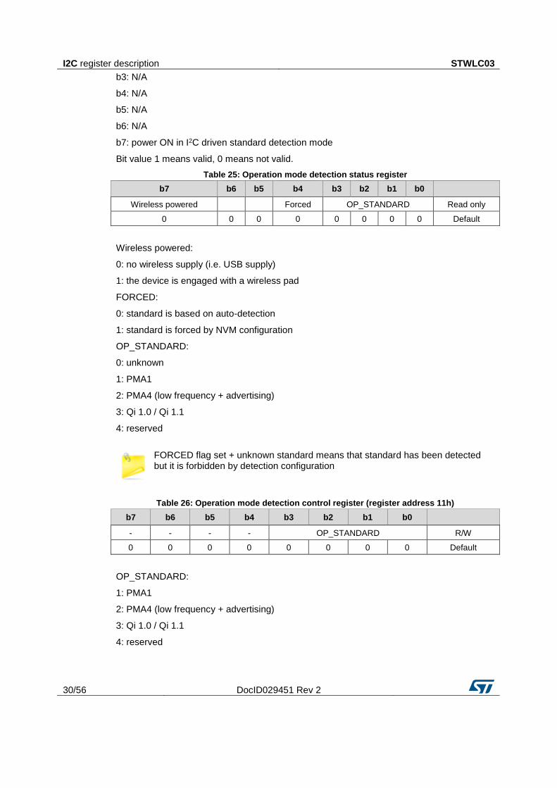
Table 25: Operation mode detection status register
b7 b6 b5 b4 b3 b2 b1 b0
Wireless powered
Forced OP_STANDARD Read only
0 0 0 0 0 0 0 0 Default
Wireless powered:
0: no wireless supply (i.e. USB supply)
1: the device is engaged with a wireless pad
FORCED:
0: standard is based on auto-detection
1: standard is forced by NVM configuration
OP_STANDARD:
0: unknown
1: PMA1
2: PMA4 (low frequency + advertising)
3: Qi 1.0 / Qi 1.1
4: reserved
FORCED flag set + unknown standard means that standard has been detected but it is forbidden by detection configuration
Table 26: Operation mode detection control register (register address 11h)
b7 b6 b5 b4 b3 b2 b1 b0
- - - - OP_STANDARD R/W
0 0 0 0 0 0 0 0 Default
OP_STANDARD:
1: PMA1
2: PMA4 (low frequency + advertising)
3: Qi 1.0 / Qi 1.1
4: reserved
STWLC03 I2C register description
DocID029451 Rev 2 31/56
This register is functional only in combination with “I2C master driven” detection configuration
Table 27: Qi charge status register (register address 12h)
b7 b6 b5 b4 b3 b2 b1 b0
Qi_CHARGE_PACKET R/W
1 1 1 1 1 1 1 1 Default
Available in Qi mode only. It contains a value that is sent to the Qi charge status packet. Values in the range from 0 to 100 provide percentage of the battery capacity. If there is no need to use the charge status packets, this register should be set to FFh.
Table 28: Charger status register (register address 13h)
b7 b6 b5 b4 b3 b2 b1 b0
CHARGER_STATUS R/W
x x x x x x x x Default
CHARGER_STATUS:
0: off
1: pre-charge
2: fast charge
3: termination counter running
4: battery OVP
Table 29: Charger control register
b7 b6 b5 b4 b3 b2 b1 b0
CHARGER_CONTROL R/W
Loaded from NVM at startup Default
CHARGER_CONTROL:
0: disabled
1: enabled
6.1 ADC measured values
Table 30: ADC measured value register map
Address Register
20-21h Rectified voltage
22-23h Rectifier output current
24-25h Rx coil NTC voltage
26-27h Output voltage
28-29h Rectifier internal drop voltage
2A-2Bh Chip temperature
I2C register description STWLC03
32/56 DocID029451 Rev 2
Address Register
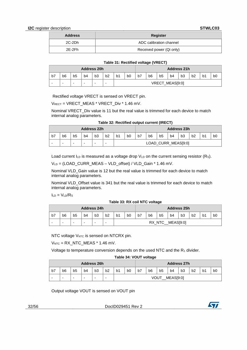
2C-2Dh ADC calibration channel
2E-2Fh Received power (Qi only)
Table 31: Rectified voltage (VRECT)
Address 20h Address 21h
b7 b6 b5 b4 b3 b2 b1 b0 b7 b6 b5 b4 b3 b2 b1 b0
- - - - - - VRECT_MEAS[9:0]
Rectified voltage VRECT is sensed on VRECT pin.
VRECT = VRECT_MEAS * VRECT_Div * 1.46 mV.
Nominal VRECT_Div value is 11 but the real value is trimmed for each device to match internal analog parameters.
Table 32: Rectified output current (IRECT)
Address 22h Address 23h
b7 b6 b5 b4 b3 b2 b1 b0 b7 b6 b5 b4 b3 b2 b1 b0
- - - - - - LOAD_CURR_MEAS[9:0]
Load current ILD is measured as a voltage drop VLD on the current sensing resistor (RS).
VLD = (LOAD_CURR_MEAS – VLD_offset) / VLD_Gain * 1.46 mV.
Nominal VLD_Gain value is 12 but the real value is trimmed for each device to match internal analog parameters.
Nominal VLD_Offset value is 341 but the real value is trimmed for each device to match internal analog parameters.
ILD = VLD/RS
Table 33: RX coil NTC voltage
Address 24h Address 25h
b7 b6 b5 b4 b3 b2 b1 b0 b7 b6 b5 b4 b3 b2 b1 b0
- - - - - - RX_NTC__MEAS[9:0]
NTC voltage VNTC is sensed on NTCRX pin.
VNTC = RX_NTC_MEAS * 1.46 mV.
Voltage to temperature conversion depends on the used NTC and the R1 divider.
Table 34: VOUT voltage
Address 26h Address 27h
b7 b6 b5 b4 b3 b2 b1 b0 b7 b6 b5 b4 b3 b2 b1 b0
- - - - - - VOUT__MEAS[9:0]
Output voltage VOUT is sensed on VOUT pin
STWLC03 I2C register description
DocID029451 Rev 2 33/56
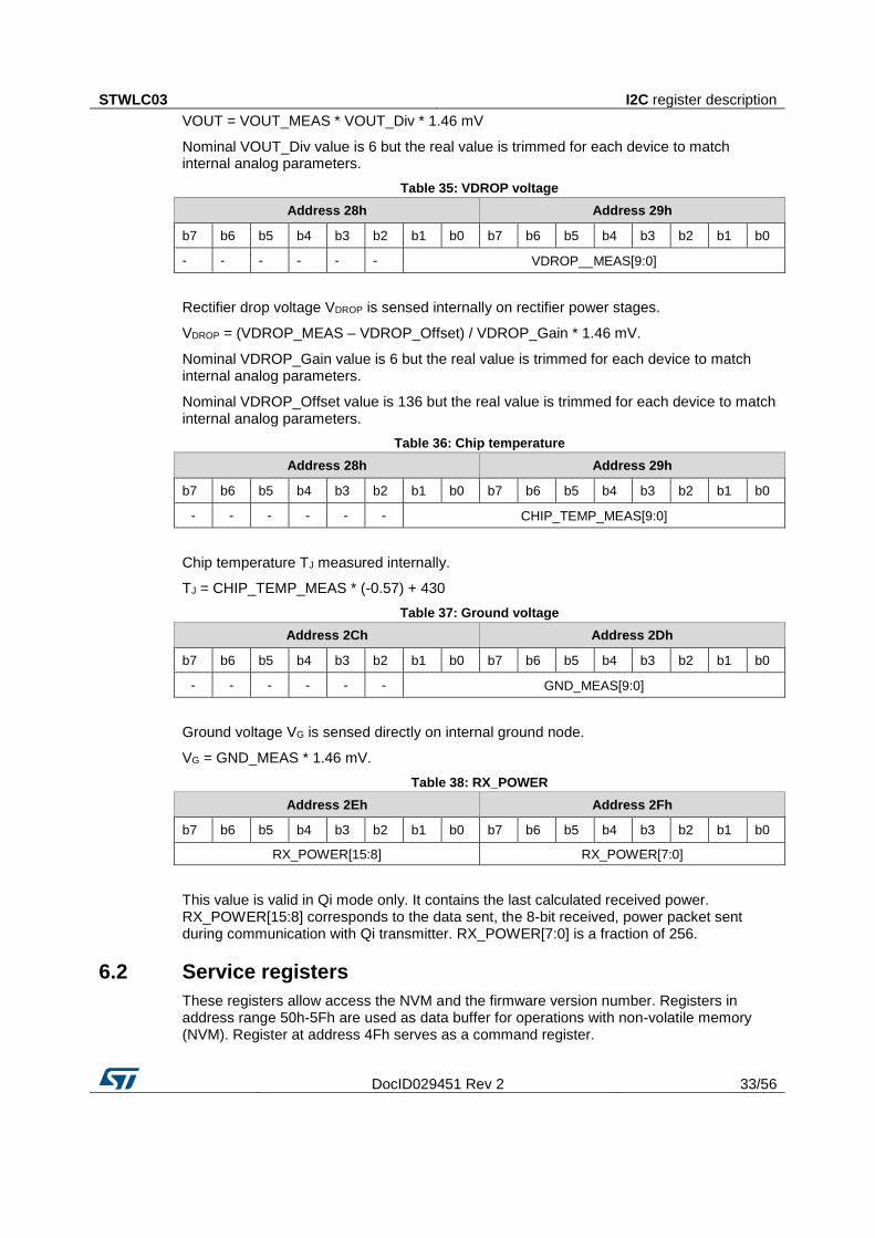
VOUT = VOUT_MEAS * VOUT_Div * 1.46 mV
Nominal VOUT_Div value is 6 but the real value is trimmed for each device to match internal analog parameters.
Table 35: VDROP voltage
Address 28h Address 29h
b7 b6 b5 b4 b3 b2 b1 b0 b7 b6 b5 b4 b3 b2 b1 b0
- - - - - - VDROP__MEAS[9:0]
Rectifier drop voltage VDROP is sensed internally on rectifier power stages.
VDROP = (VDROP_MEAS – VDROP_Offset) / VDROP_Gain * 1.46 mV.
Nominal VDROP_Gain value is 6 but the real value is trimmed for each device to match internal analog parameters.
Nominal VDROP_Offset value is 136 but the real value is trimmed for each device to match internal analog parameters.
Table 36: Chip temperature
Address 28h Address 29h
b7 b6 b5 b4 b3 b2 b1 b0 b7 b6 b5 b4 b3 b2 b1 b0
- - - - - - CHIP_TEMP_MEAS[9:0]
Chip temperature TJ measured internally.
TJ = CHIP_TEMP_MEAS * (-0.57) + 430
Table 37: Ground voltage
Address 2Ch Address 2Dh
b7 b6 b5 b4 b3 b2 b1 b0 b7 b6 b5 b4 b3 b2 b1 b0
- - - - - - GND_MEAS[9:0]
Ground voltage VG is sensed directly on internal ground node.
VG = GND_MEAS * 1.46 mV.
Table 38: RX_POWER
Address 2Eh Address 2Fh
b7 b6 b5 b4 b3 b2 b1 b0 b7 b6 b5 b4 b3 b2 b1 b0
RX_POWER[15:8] RX_POWER[7:0]
This value is valid in Qi mode only. It contains the last calculated received power. RX_POWER[15:8] corresponds to the data sent, the 8-bit received, power packet sent during communication with Qi transmitter. RX_POWER[7:0] is a fraction of 256.
6.2 Service registers
These registers allow access the NVM and the firmware version number. Registers in address range 50h-5Fh are used as data buffer for operations with non-volatile memory (NVM). Register at address 4Fh serves as a command register.

I2C register description STWLC03
34/56 DocID029451 Rev 2
Table 39: Service register map
Address Register
40h Firmware version
4Fh NVM control
50-5Fh Data manipulation registers
Table 40: NVM control
b7 b6 b5 b4 b3 b2 b1 b0
NVM_WR NVM_RD
NVM_SECT[3:0] R/W
0 0 0 0 0 0 0 0 Default
NVM_WR bit:
0: no action
1: write data into NVM sector (auto-clear)
NVM_RD bit:
0: no action
1: read data from NVM sector (auto-clear)
NVM_SECT contains the address of the sector in the NVM, which should be used for reading or writing operations.
Data to write must be prepared in data manipulation registers before starting writing operation into the control register.
Byte 00 of the NVM sector is located in data manipulation register address 50h, byte 01 in register 51h etc. according to the following table:
Table 41: I2C registers corresponding to bytes in NVM sector
Data
manipulation
register
50 51 52 53 54 55 56 57 58 59 5A 5B 5C 5D 5E 5F
NVM byte 00 01 02 03 04 05 06 07 08 09 0A 0B 0C 0D 0E 0F
STWLC03 Non-volatile memory
DocID029451 Rev 2 35/56
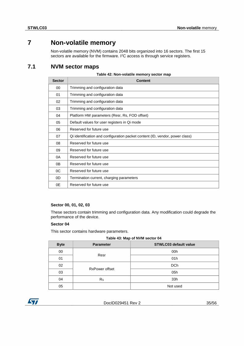
7 Non-volatile memory
Non-volatile memory (NVM) contains 2048 bits organized into 16 sectors. The first 15 sectors are available for the firmware. I2C access is through service registers.
7.1 NVM sector maps
Table 42: Non-volatile memory sector map
Sector Content
00 Trimming and configuration data
01 Trimming and configuration data
02 Trimming and configuration data
03 Trimming and configuration data
04 Platform HW parameters (Resr, Rs, FOD offset)
05 Default values for user registers in Qi mode
06 Reserved for future use
07 Qi identification and configuration packet content (ID, vendor, power class)
08 Reserved for future use
09 Reserved for future use
0A Reserved for future use
0B Reserved for future use
0C Reserved for future use
0D Termination current, charging parameters
0E Reserved for future use
Sector 00, 01, 02, 03
These sectors contain trimming and configuration data. Any modification could degrade the performance of the device.
Sector 04
This sector contains hardware parameters.
Table 43: Map of NVM sector 04
Byte Parameter STWLC03 default value
00 Resr
00h
01 01h
02 RxPower offset
DCh
03 05h
04 RS 33h
05
Not used

Non-volatile memory STWLC03
36/56 DocID029451 Rev 2
Byte Parameter STWLC03 default value
06
07
08
09
10
11
12
13
14
15
Table 44: Byte 0
Byte 0
b7 b6 b5 b4 b3 b2 b1 b0
Resr [7:0] (LSB)
Table 45: Byte 1
Byte 1
b7 b6 b5 b4 b3 b2 b1 b0
Resr [15:8] (MSB)
Rx coil resistance. Resr is a 16 bit unsigned valued in Ohm multiplied by 1024. This value is used when power losses are estimated during RxPower calculation in Qi mode.
Table 46: Byte 2
Byte 2
b7 b6 b5 b4 b3 b2 b1 b0
RxPower offset [7:0] (LSB)
Table 47: Byte 3
Byte 3
b7 b6 b5 b4 b3 b2 b1 b0
RxPower offset [15:8] (MSB)
RxPower offset is a 16-bit signed value that is added to the RxPower calculated in Qi mode. It tunes the accuracy and compensates potential additional losses in the magnetic field caused by a presence of other objects such as the PCB or battery.
STWLC03 Non-volatile memory
DocID029451 Rev 2 37/56
Table 48: Byte 4
Byte 4
b7 b6 b5 b4 b3 b2 b1 b0
Rs[7:0]
This parameter represents the value of the current sensing resistor RS in Ohm multiplied by 1024. This value is necessary for RxPower calculation in Qi mode.
Sector 05
This sector contains default register values for Qi mode that are loaded into internal I2C registers after the startup of the microcontroller.
Table 49: Map of NVM sector 05
Byte Target I2C register STWLC03 default value
00 00h 01h
01 01h 0Fh
02 02h 18h
03 03h 00h
04 04h 01h
05 05h 4Eh
06 06h 05h
07 07h 04h
08 08h 04h
09 09h 80h
10 0Ah 00h
11 0Bh 00h
12
Not used 13
14
15
Sector 06
This sector is reserved for future use.
Sector 07
This sector contains data used in identification and configuration packets in Qi mode.

Non-volatile memory STWLC03
38/56 DocID029451 Rev 2
Table 50: Map of NVM sector 07
Byte Parameter STWLC03 default value
00 Manufacturer code MSB 00h
01 Manufacturer code LSB 16h
02 Basic device identifier MSB 01h
03 Basic device identifier 02h
04 Basic device identifier 03h
05 Basic device identifier LSB 04h
06 Extended device identifier MSB 11h
07 Extended device identifier 12h
08 Extended device identifier 13h
09 Extended device identifier 14h
10 Extended device identifier 15h
11 Extended device identifier 16h
12 Extended device identifier 17h
13 Extended device identifier LSB 18h
14 Maximum power 0Ah
15 Unused 00h
Sector 08
This sector contains default register values for PMA mode that are loaded into internal I2C registers after start-up of the microcontroller.

STWLC03 Non-volatile memory
DocID029451 Rev 2 39/56
Table 51: Map of NVM sector 08
Byte Target I2C register STWLC03 default value
00 00h 01h
01 01h 19h
02 02h 1Dh
03 03h 01h
04 04h 0Ah
05 05h C3h
06 06h 09h
07 07h 04h
08 08h 0Dh
09 09h 7Ah
10 0Ah 00h
11 0Bh 00h
12
Not used
13
Not used
14
Not used
15
Not used
Sector 09
This sector is reserved for future use.
Sector 10
This sector contains PMA RXID and its CRC.
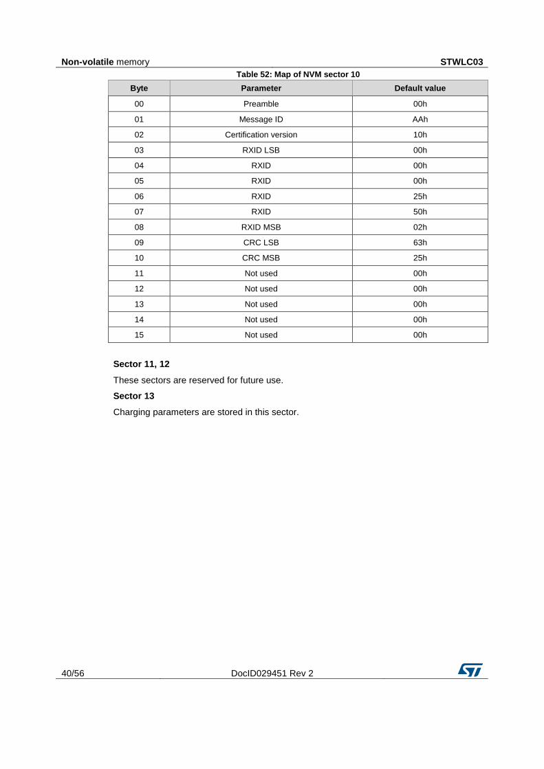
Non-volatile memory STWLC03
40/56 DocID029451 Rev 2
Table 52: Map of NVM sector 10
Byte Parameter Default value
00 Preamble 00h
01 Message ID AAh
02 Certification version 10h
03 RXID LSB 00h
04 RXID 00h
05 RXID 00h
06 RXID 25h
07 RXID 50h
08 RXID MSB 02h
09 CRC LSB 63h
10 CRC MSB 25h
11 Not used 00h
12 Not used 00h
13 Not used 00h
14 Not used 00h
15 Not used 00h
Sector 11, 12
These sectors are reserved for future use.
Sector 13
Charging parameters are stored in this sector.

STWLC03 Non-volatile memory
DocID029451 Rev 2 41/56
Table 53: Map of NVM sector 13
Byte STWLC03 default value
00 26h
01 24h
02 03h
03 4Ch
04 CCh
05 Not used
06 Not used
07 Not used
08 4Dh
09 24h
10 03h
11 4Ch
12 CCh
13 Not used
14 Not used
15 Not used
Table 54: Byte 0 Qi_EPT_threshold [7:0]
Byte 0
b7 b6 b5 b4 b3 b2 b1 b0
Qi_EPT_threshold [7:0]
It sets the threshold for charging termination. Current has not be sensed on the output but on RS sensing resistor.
Qi_EPT_threshold is directly compared with (LOAD_CURR_MEAS/2).
This parameter is active both in fixed output voltage mode and in charger mode.
Table 55: Byte 1, Qi_EPT_Time [7:0]
Byte 1
b7 b6 b5 b4 b3 b2 b1 b0
Qi_EPT_Time [7:0]
Qi_EPT_Time is end-of-power transfer deglitch time in minutes. If the charging current is permanently lower than Qi_EPT_threshold for more than Qi_EPT_Time, the end-of-power transfer packet is sent to the transmitter.

Non-volatile memory STWLC03
42/56 DocID029451 Rev 2
This parameter is active both in fixed output voltage mode and in charger mode.
Table 56: Byte 2, Qi charger enable
Byte 2
b7 b6 b5 b4 b3 b2 b1 b0
Qi charger enable - - - - Qi target voltage [2:0]
Qi charger enable bit:
0: charging algorithm is not active after startup
1: charging algorithm is active after startup
Table 57: Qi target voltage
Qi target voltage Charging voltage [V]
0 3.3
1 3.6
2 4.1
3 4.2
4 5.0
Table 58: Byte 3, Q1_Precharge_Battery_overvoltage
Byte 3
b7 b6 b5 b4 b3 b2 b1 b0
Qi_Precharge_voltage [1:0] Qi_Battery_overvoltage [5:0]
Qi_Precharge_voltage:
00b: 2.5 V
01b: 2.7 V
10b: 2.9 V
11b: 3.1 V
Battery OVP threshold = (3.3 V + Qi_Battery_overvoltage * 100 mV) / 1024 * 1000
Table 59: Byte 4, Q1_Precharge and Fastcharge
Byte 4
b7 b6 b5 b4 b3 b2 b1 b0
Qi_Precharge_current [1:0] Qi_Fastcharge_current [5:0]
Qi_Precharge_current
00b: 2.5 mV / RS (50 mA @ 50 mΩ RS)
01b: 5 mV / RS (100 mA @ 50 mΩ RS)
10b: 7.5 mV / RS (150 mA @ 50 mΩ RS)

STWLC03 Non-volatile memory
DocID029451 Rev 2 43/56
11b: 10 mV / RS (200 mA @ 50 mΩ RS)
Qi Fastcharge current = (Qi_Fastcharge_current * 2.5 mV + 5 mV) / RS
Table 60: Byte 8, PMA_EOC_theshold [7:0]
Byte 8
b7 b6 b5 b4 b3 b2 b1 b0
PMA_EOC_theshold [7:0]
It sets the threshold for charging termination. Current has not be sensed on the output but on RS sensing resistor.
PMA_EOC_threshold is directly compared with (LOAD_CURR_MEAS / 2).
This parameter is active both in fixed output voltage mode and in charger mode.
Table 61: Byte 9, PMA_EOC_Time [7:0]
Byte 9
b7 b6 b5 b4 b3 b2 b1 b0
PMA_EOC_Time [7:0]
PMA_EOC_Time is end-of-power transfer deglitch time in minutes. If the charging current is permanently lower than PMA_EOC_theshold for more PMA_EOC_Time, the end-of-charging signal is sent to the transmitter.
This parameter is active both in fixed output voltage mode and in charger mode.
Table 62: Byte 10, PMA_Target_Voltage [2:0]
Byte 10
b7 b6 b5 b4 b3 b2 b1 b0
PMA charger enable - - - - PMA_ Target_Voltage [2:0]
PMA charger enable bit:
0: charging algorithm is not active after startup
1: charging algorithm is active after startup
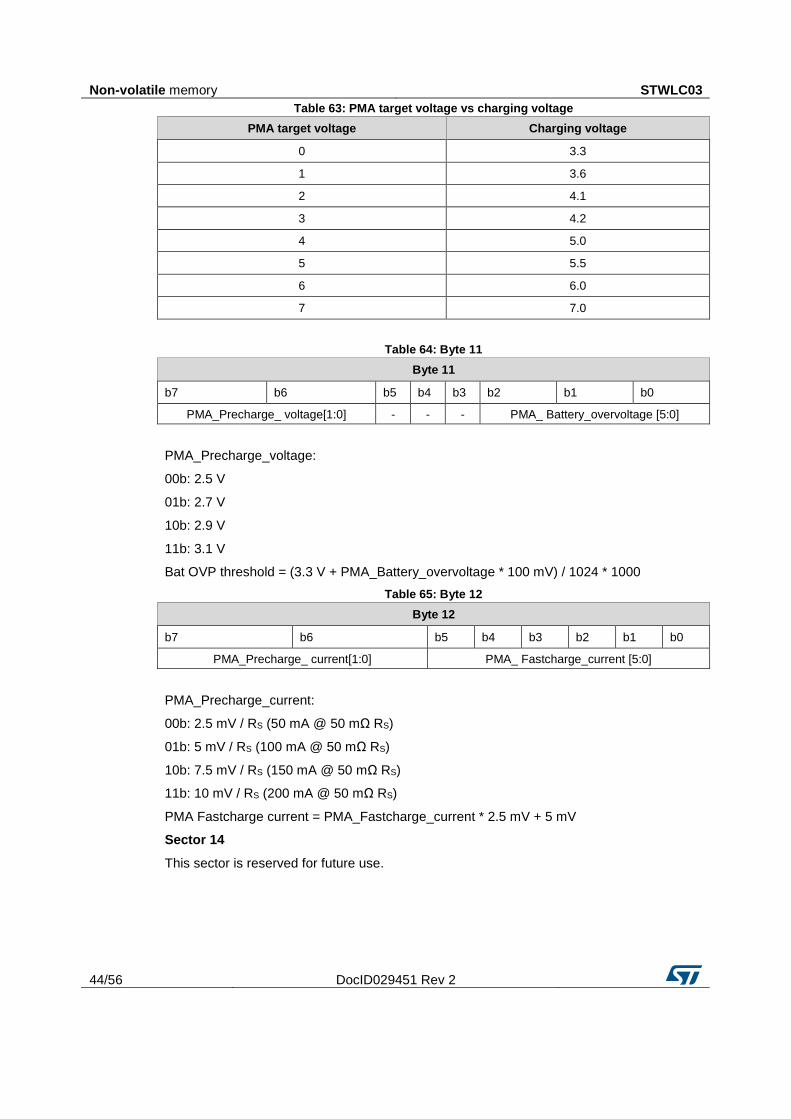
Non-volatile memory STWLC03
44/56 DocID029451 Rev 2
Table 63: PMA target voltage vs charging voltage
PMA target voltage Charging voltage
0 3.3
1 3.6
2 4.1
3 4.2
4 5.0
5 5.5
6 6.0
7 7.0
Table 64: Byte 11
Byte 11
b7 b6 b5 b4 b3 b2 b1 b0
PMA_Precharge_ voltage[1:0] - - - PMA_ Battery_overvoltage [5:0]
PMA_Precharge_voltage:
00b: 2.5 V
01b: 2.7 V
10b: 2.9 V
11b: 3.1 V
Bat OVP threshold = (3.3 V + PMA_Battery_overvoltage * 100 mV) / 1024 * 1000
Table 65: Byte 12
Byte 12
b7 b6 b5 b4 b3 b2 b1 b0
PMA_Precharge_ current[1:0] PMA_ Fastcharge_current [5:0]
PMA_Precharge_current:
00b: 2.5 mV / RS (50 mA @ 50 mΩ RS)
01b: 5 mV / RS (100 mA @ 50 mΩ RS)
10b: 7.5 mV / RS (150 mA @ 50 mΩ RS)
11b: 10 mV / RS (200 mA @ 50 mΩ RS)
PMA Fastcharge current = PMA_Fastcharge_current * 2.5 mV + 5 mV
Sector 14
This sector is reserved for future use.

STWLC03 Application information
DocID029451 Rev 2 45/56
8 Application information
8.1 Application schematic and recommended external components
Figure 10: STWLC03 application schematic
RM is an optional component and it is not needed for a typical application. If VEXT detection is disabled, C8 and TRSWDRV are optional.

Application information STWLC03
46/56 DocID029451 Rev 2
Figure 11: STWLC03 charger configuration
Before connecting the battery, the STWLC03 has to be configured as a battery charger in NVM.
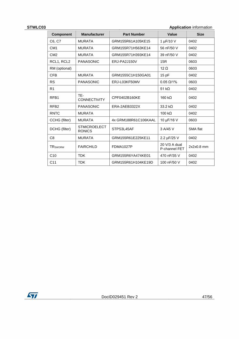
Table 66: STWLC03 recommended external components
Component Manufacturer Part Number Value Size
L1 Wurth 760308103215 14.3 uH 48x32x1 mm
TDK 760308103202 12 μH 48x32x1 mm
L2
TOKO DFE252012F-1R5 1.5 μH/3.8 A 2.5x2.0x1.2 mm
CYNTEC PILE25201D-2R2MS-11 2.2 μH/3.1 A
2.5x2.0x1.4 mm
PIME041B-2R2MS-11 2.2 μH/4.3 A 4.4x4.2x1 mm
TDK SPM3010T-1R0 1 μH/4.5 A 3x3.2x1mm
TFM1R0GHM 1 μH 2x1.6x1 mm
C1 MURATA 3x GRM188R72A104KA35 100 nF/X7R 0603
C2 MURATA GRM155R71H332KA01 3.3 nF/C0G 0603
C3 MURATA 2x GRM188R61C106KAAL 10 μF/16 V 0603
TDK 2x C1608X5R1C106M 10 μF/16 V 0603
C4 MURATA GRM188R61C106KAAL 10 μF/16 V 0603
CBOOT1, CBOOT2, CBOOT
MURATA GRM155R61H473KE14 47 nF/50 V 0402
C5 MURATA 2x GRM188R61C106KAAL 10 µF/16 V 0603
STWLC03 Application information
DocID029451 Rev 2 47/56
Component Manufacturer Part Number Value Size
C6, C7 MURATA GRM155R61A105KE15 1 µF/10 V 0402
CM1 MURATA GRM155R71H563KE14 56 nF/50 V 0402
CM2 MURATA GRM155R71H393KE14 39 nF/50 V 0402
RCL1, RCL2 PANASONIC ERJ-PA2J150V 15R 0603
RM (optional)
12 Ω 0603
CFB MURATA GRM1555C1H150GA01 15 pF 0402
RS PANASONIC ERJ-L03KF50MV 0.05 Ω/1% 0603
R1
51 kΩ 0402
RFB1 TE-CONNECTIVITY
CPF0402B160KE 160 kΩ 0402
RFB2 PANASONIC ERA-2AEB3322X 33.2 kΩ 0402
RNTC MURATA
100 kΩ 0402
CCHG (filter) MURATA 4x GRM188R61C106KAAL 10 μF/16 V 0603
DCHG (filter) STMICROELECTRONICS
STPS3L45AF 3 A/45 V SMA flat
C8 MURATA GRM155R61E225KE11 2.2 µF/25 V 0402
TRSWDRW FAIRCHILD FDMA1027P 20 V/3 A dual P-channel FET
2x2x0.8 mm
C10 TDK GRM155R6YA474KE01 470 nF/35 V 0402
C11 TDK GRM155R61H104KE19D 100 nF/50 V 0402

Application information STWLC03
48/56 DocID029451 Rev 2
Figure 12: VIO and digital interface in standalone application schematic
Figure 13: VIO and digital interface in platform application schematic
STWLC03 Application information
DocID029451 Rev 2 49/56
8.2 External passive component selection
8.2.1 Input resonant circuit component selection (L1, C1, C2)
The selected RX coil should be optimized by the requested transferred power. The inductance of the coil together with C1 and C2 capacitors create an input resonant circuit. Components have to be carefully selected both to keep the resonant frequency compliant with the wireless standard specification and to deliver the power. For more details please see wireless standard specifications.
The following equations show the resonant frequencies, where L1’ is self-inductance of L1 placed on the transmitter:
Equation 1:
𝑓𝑠 =1
2 ∗ 𝜋 ∗ √𝐿1′ ∗ 𝐶1
Equation 2:
𝑓𝐷 =1
2 ∗ 𝜋 ∗ √𝐿1 ∗ (1𝐶1
+1𝐶2)−1
It is recommended to use high grade ceramic capacitors with C0G dielectrics type. X5R, X7R capacitors can be used for 5 W output power applications.
8.2.2 Voltage clamp resistor selection (RCL1, RCL2)
The purpose of these resistors is to load the rectifier output by decreasing the rectified voltage below overvoltage threshold – hysteresis (VOVP-VOVPHYST), when VOVP is reached. 0.2 W resistors with pulse withstanding character are recommended for this application.
8.2.3 Load modulation capacitors selection (CM1, CM2)
These capacitors fulfill the backscatter modulation of the communication from the receiver to the transmitter. X5R dielectrics type capacitors are suitable for this purpose. Higher values of these capacitors help to comply to PMA standard, but increase the ripple in the system.
8.2.4 Feedback resistor divider components selection (RFB1, RFB2)
Feedback voltage divider gives the ratio between the desired step-down converter output voltage and the given feedback reference voltage. The RFB1 and RFB2 resistors should be 0.1% or 0.5% tolerance class.
8.2.5 Rx NTC circuit component selection (RNTC, R1)
To protect the receiver coil from overtemperature, the STWLC03 is equipped with a comparator input. If the input voltage crosses certain level (see Table 4: "Thermal data"), the STWLC03 can react by terminating the power transfer and sending an interrupt to the host system – depending on the configuration. The input voltage given as a ratio from RNTC thermistor and R1 common resistor divider. The divider can be supplied from LDO1 (VA pin) filtering capacitor.

Application information STWLC03
50/56 DocID029451 Rev 2
8.2.6 Soft-start capacitor selection (C10)
The soft-start capacitor C10 connected to COMP pin influences the ramp-up time of the step-down converter. The nominal VREF voltage is 1.2 V and the time needed to reach the nominal voltage is given by the following equation:
Equation 3:
𝑡𝑆𝑂𝐹𝑇𝑆𝑇𝐴𝑅𝑇 = 𝐶 ∙ 106 ∙ 𝑉𝑅𝐸𝐹[𝑠, 𝐹, −, 𝑉]
Example: 470 nF ~ 560 ms
8.2.7 External supply transistor selection
The device contains the function of the connection external voltage supply directly to VOUT by the external dual P-channel transistor back-to-back connected so to avoid the leakage from VOUT to the external voltage supply.
STWLC03 Application information
DocID029451 Rev 2 51/56
8.3 Reference PCB layout
Figure 14: Top overlay
Figure 15: Top layer
Figure 16: Mid layer 1
Figure 17: Mid layer 2
Application information STWLC03
52/56 DocID029451 Rev 2
Figure 18: Bottom layer

STWLC03 Package information
DocID029451 Rev 2 53/56
9 Package information
In order to meet environmental requirements, ST offers these devices in different grades of ECOPACK® packages, depending on their level of environmental compliance. ECOPACK® specifications, grade definitions and product status are available at: www.st.com. ECOPACK® is an ST trademark.
9.1 Flip Chip 77 bumps (3.12x4.73 mm) package information
Figure 19: Flip Chip 77 bumps (3.12x4.73 mm) package outline
Package information STWLC03
54/56 DocID029451 Rev 2
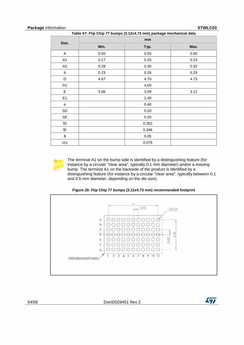
Table 67: Flip Chip 77 bumps (3.12x4.73 mm) package mechanical data
Dim. mm
Min. Typ. Max.
A 0.50 0.55 0.60
A1 0.17 0.20 0.23
A2 0.28 0.30 0.32
b 0.23 0.26 0.29
D 4.67 4.70 4.73
D1
4.00
E 3.06 3.09 3.12
E1
2.40
e
0.40
SD
0.20
SE
0.20
fD
0.352
fE
0.346
$
0.05
ccc
0.075
The terminal A1 on the bump side is identified by a distinguishing feature (for instance by a circular "clear area", typically 0.1 mm diameter) and/or a missing bump. The terminal A1 on the backside of the product is identified by a distinguishing feature (for instance by a circular "clear area", typically between 0.1 and 0.5 mm diameter, depending on the die size).
Figure 20: Flip Chip 77 bumps (3.12x4.73 mm) recommended footprint

STWLC03 Revision history
DocID029451 Rev 2 55/56
10 Revision history Table 68: Document revision history
Date Revision Changes
09-Nov-2016 1 Initial release.
14-Mar-2017 2 Updated Section 8.2.1: "Input resonant circuit component selection
(L1, C1, C2)".
STWLC03
56/56 DocID029451 Rev 2
IMPORTANT NOTICE – PLEASE READ CAREFULLY
STMicroelectronics NV and its subsidiaries (“ST”) reserve the right to make changes, corrections, enhancements, modifications , and improvements to ST products and/or to this document at any time without notice. Purchasers should obtain the latest relevant information on ST products before placing orders. ST products are sold pursuant to ST’s terms and conditions of sale in place at the time of order acknowledgement.
Purchasers are solely responsible for the choice, selection, and use of ST products and ST assumes no liability for application assistance or the design of Purchasers’ products.
No license, express or implied, to any intellectual property right is granted by ST herein.
Resale of ST products with provisions different from the information set forth herein shall void any warranty granted by ST for such product.
ST and the ST logo are trademarks of ST. All other product or service names are the property of their respective owners.
Information in this document supersedes and replaces information previously supplied in any prior versions of this document.
© 2017 STMicroelectronics – All rights reserved
Related Documents