User's Guide SLOU355 – March 2013 DRV2604 ERM, LRA Haptic Driver Evaluation Kit The DRV2604 is a haptic driver designed for Linear Resonant Actuators (LRA) and Eccentric Rotating Mass (ERM) motors. It provides many features which help eliminate the design complexities of haptic motor control including reduced solution size, high efficiency output drive, closed-loop motor control, quick device startup, memory for waveform storage, and auto-resonance frequency tracking. The DRV2604EVM-CT Evaluation Module (EVM) is a complete demo and evaluation platform for the DRV2604. The kit includes a microcontroller, linear actuator, eccentric rotating mass motor, and capacitive touch buttons which can be used to completely demonstrate and evaluate the DRV2604. This document contains instructions to setup and operate the DRV2604EVM-CT in demo and evaluation mode. Figure 1. DRV2604EVM-CT Board Evaluation Kit Contents: • DRV2604EVM-CT demo and evaluation board • Mini-USB cable • Demonstration Firmware Required for programming and advanced configuration: • Code Composer Studio™ (CCS) or IAR Embedded Workbench IDE for MSP430 • MSP430 LaunchPad (MSP-EXP430G2), or MSP430-FET430UIF hardware programming tool • DRV2604EVM-CT firmware available on ti.com Code Composer Studio is a trademark of Texas Instruments. I 2 C is a trademark of NXP. 1 SLOU355 – March 2013 DRV2604 ERM, LRA Haptic Driver Evaluation Kit Submit Documentation Feedback Copyright © 2013, Texas Instruments Incorporated

Welcome message from author
This document is posted to help you gain knowledge. Please leave a comment to let me know what you think about it! Share it to your friends and learn new things together.
Transcript

User's GuideSLOU355–March 2013
DRV2604 ERM, LRA Haptic Driver Evaluation Kit
The DRV2604 is a haptic driver designed for Linear Resonant Actuators (LRA) and Eccentric RotatingMass (ERM) motors. It provides many features which help eliminate the design complexities of hapticmotor control including reduced solution size, high efficiency output drive, closed-loop motor control, quickdevice startup, memory for waveform storage, and auto-resonance frequency tracking.
The DRV2604EVM-CT Evaluation Module (EVM) is a complete demo and evaluation platform for theDRV2604. The kit includes a microcontroller, linear actuator, eccentric rotating mass motor, and capacitivetouch buttons which can be used to completely demonstrate and evaluate the DRV2604.
This document contains instructions to setup and operate the DRV2604EVM-CT in demo and evaluationmode.
Figure 1. DRV2604EVM-CT Board
Evaluation Kit Contents:• DRV2604EVM-CT demo and evaluation board
• Mini-USB cable
• Demonstration Firmware
Required for programming and advanced configuration:
• Code Composer Studio™ (CCS) or IAR Embedded Workbench IDE for MSP430
• MSP430 LaunchPad (MSP-EXP430G2), or MSP430-FET430UIF hardware programming tool
• DRV2604EVM-CT firmware available on ti.com
Code Composer Studio is a trademark of Texas Instruments.I2C is a trademark of NXP.
1SLOU355–March 2013 DRV2604 ERM, LRA Haptic Driver Evaluation KitSubmit Documentation Feedback
Copyright © 2013, Texas Instruments Incorporated

www.ti.com
Contents1 Getting Started .............................................................................................................. 4
1.1 Evaluation Module Operating Parameters ...................................................................... 51.2 Quick Start Board Setup .......................................................................................... 5
2 DRV2604 Demonstration Program ....................................................................................... 62.1 Modes and Effects Table ......................................................................................... 62.2 Description of the Demo Modes ................................................................................. 72.3 RAM Library Mode ............................................................................................... 102.4 Waveform Library Effects List ................................................................................... 10
3 Additional Hardware Modes .............................................................................................. 113.1 Enter Binary Counting Mode .................................................................................... 113.2 Exit Binary Counting Mode ...................................................................................... 113.3 Binary Counting Modes .......................................................................................... 12
4 Hardware Configuration .................................................................................................. 134.1 Input and Output Overview ...................................................................................... 134.2 Power Supply Selection ......................................................................................... 134.3 Using an External Actuator ...................................................................................... 144.4 PWM Input ......................................................................................................... 144.5 External Trigger Control ......................................................................................... 154.6 External I2C Input ................................................................................................. 164.7 Analog Input ....................................................................................................... 17
5 Measurement and Analysis .............................................................................................. 176 Modifying or Reprogramming the Firmware ........................................................................... 19
6.1 MSP430 Pin-Out .................................................................................................. 207 Schematic .................................................................................................................. 218 Layout ....................................................................................................................... 229 Bill of Materials ............................................................................................................. 25
List of Figures
1 DRV2604EVM-CT Board .................................................................................................. 1
2 Board Diagram .............................................................................................................. 4
3 ERM Click and Bounce Waveform (Button 1)........................................................................... 7
4 LRA Ramp-Up and Click Waveform (Button 2) ......................................................................... 7
5 ERM Closed-Loop Click Waveform (Button 1) .......................................................................... 7
6 ERM Open-Loop Click Waveform (Button 4)............................................................................ 7
7 LRA Closed-Loop Click Waveform (Button 1)........................................................................... 8
8 LRA Open-Loop Click Waveform (Button 4) ............................................................................ 8
9 LRA Auto-Resonance ON Waveform (Button 1)........................................................................ 8
10 LRA Auto-Resonance OFF Waveform (Button 2) ...................................................................... 8
11 Acceleration Versus Frequency ........................................................................................... 9
12 LRA Scroll Wheel Effect Waveform (Button 4).......................................................................... 9
13 Power Jumper Selection.................................................................................................. 13
14 Terminal Block and Test Points ......................................................................................... 14
15 External PWM Input ....................................................................................................... 14
16 External Trigger Control .................................................................................................. 15
17 External I2C Input .......................................................................................................... 16
18 Analog Input................................................................................................................ 17
19 Terminal Block and Test Points ......................................................................................... 17
20 DRV2604 Unfiltered Waveform.......................................................................................... 18
21 DRV2604 Filtered Waveform ............................................................................................ 18
22 Measuring the DRV2604 Output Signal with an Analog Low-Pass Filter .......................................... 18
23 LaunchPad Programmer Connection ................................................................................... 19
2 DRV2604 ERM, LRA Haptic Driver Evaluation Kit SLOU355–March 2013Submit Documentation Feedback
Copyright © 2013, Texas Instruments Incorporated
www.ti.com
24 DRV2604EVM-CT Schematic............................................................................................ 21
25 X-Ray Top View ........................................................................................................... 22
26 Top Copper................................................................................................................. 22
27 Layer 2 Copper ............................................................................................................ 23
28 Layer 3 Copper ............................................................................................................ 23
29 Bottom Copper............................................................................................................. 24
List of Tables
1 Mode and Effects Table.................................................................................................... 6
2 Binary Counting Modes................................................................................................... 12
3 Hardware Overview ....................................................................................................... 13
4 MSP430 Pin-Out........................................................................................................... 20
3SLOU355–March 2013 DRV2604 ERM, LRA Haptic Driver Evaluation KitSubmit Documentation Feedback
Copyright © 2013, Texas Instruments Incorporated
ActuatorsDRV2604
MSP430
OUT
US
B
VB
AT
SB
W
MSP
DRV
USB Power
External Power
Power Select Pins
DRV2604 Increment Mode
Decrement Mode ERM and LRA Actuators
Effect ButtonsPress to play haptic effects.
Programmer Connector
AUDIO
Analog-In
JP4
JP3
Actuator Disconnect
Getting Started www.ti.com
1 Getting Started
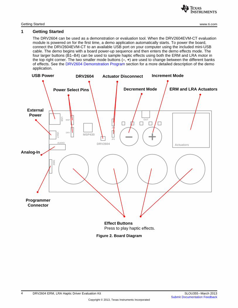
The DRV2604 can be used as a demonstration or evaluation tool. When the DRV2604EVM-CT evaluationmodule is powered on for the first time, a demo application automatically starts. To power the board,connect the DRV2604EVM-CT to an available USB port on your computer using the included mini-USBcable. The demo begins with a board power-up sequence and then enters the demo effects mode. Thefour larger buttons (B1–B4) can be used to sample haptic effects using both the ERM and LRA motor inthe top right corner. The two smaller mode buttons (–, +) are used to change between the different banksof effects. See the DRV2604 Demonstration Program section for a more detailed description of the demoapplication.
Figure 2. Board Diagram
4 DRV2604 ERM, LRA Haptic Driver Evaluation Kit SLOU355–March 2013Submit Documentation Feedback
Copyright © 2013, Texas Instruments Incorporated

www.ti.com Getting Started
1.1 Evaluation Module Operating Parameters
The following table lists the operating conditions for the DRV2604 on the evaluation module.
Parameter Specification
Supply voltage range 2.5 V to 5. 5 V
Power-supply current rating 400 mA
1.2 Quick Start Board Setup
The DRV2604EVM-CT firmware contains haptic waveforms which showcase the features and benefits ofthe DRV2604. Follow the instructions below to begin the demo:
1. Out of the box, the jumpers are set to begin demo mode using USB power. The default jumper settingsare found in the table below.
Jumper Default Position Description
JP1 Shorted Connect MSP430 GPIO/PWM output to DRV2604 IN/TRIG
JP2 Shorted 3.3 V reference for I2C™
JP3, JP4 Shorted Connect on-board actuators to DRV2604
MSP USB to MSP Select USB (5 V) or VBAT power for the MSP430
DRV USB to DRV Select USB (5 V) or VBAT power for the DRV2604
2. Connect the included mini-USB cable to the USB connector on the DRV2604EVM-CT board.
3. Connect the other end of the USB cable to an available USB port on a computer, USB charger, or USBbattery pack.
4. If the board is powered correctly, the four colored LEDs will turn on, the four mode LEDs will flash, andthe LRA and ERM will perform auto-calibration, indicating the board has been successfully initialized.
5SLOU355–March 2013 DRV2604 ERM, LRA Haptic Driver Evaluation KitSubmit Documentation Feedback
Copyright © 2013, Texas Instruments Incorporated

DRV2604 Demonstration Program www.ti.com
2 DRV2604 Demonstration Program
The sections below provide a detailed description of the demo modes and effects.
2.1 Modes and Effects Table
The effects preloaded on the DRV2604EVM-CT are listed in Table 1. The modes are selected using the +and – mode buttons in the center of the board. The current mode is identified by the white LEDs directlyabove the mode buttons. Buttons B1–B4 trigger the effects listed in the description column and changebased on the selected mode.
Table 1. Mode and Effects Table
Mode Button Description Actuator Waveform InterfaceLocation
Mode Off B1 Click + Bounce ERM RAM Internal Trigger (I2C)LEDs Off B2 Ramp Up + Click LRA
B3 Gallop Alert ERM
B4 Pulsing Alert LRA
Mode 4 B1 Strong Click ERM RAM Ext. Level Trig.LED M4 On B2 Bump + Release Internal Trigger
B3 Double Strong Click Ext. Edge Trig.
B4 Click (Open Loop) µController PWM
Mode 3 B1 Strong Click LRA RAM Ext. Level Trig.LED M3 On B2 Bump + Release Internal Trigger
B3 Double Strong Click Ext. Level Trig.
B4 Click (Open Loop) µController PWM
Mode 2 B1 Buzz Auto-Resonance ON LRA µController RTP (I2C)LED M2 On B2 Buzz Auto-Resonance OFF PWM
B3 Buzz Alert ERM
B4 Scroll Wheel LRA RTP (I2C)
Mode 1 B1 Concentration Game ERM and LRA RAM Internal Trigger (I2C)LED M1 On The board will display a pattern usingB2
the effect buttons. See how manyB3 times you can repeat the pattern as it
increases by one effect each time.B4
Mode 0 B1 Auto-Calibration ERM Internal Routine Internal Trigger (I2C)LED M0 On B2 Auto-Calibration LRA
B3 Click ERM/LRA RAM
B4 Buzz
6 DRV2604 ERM, LRA Haptic Driver Evaluation Kit SLOU355–March 2013Submit Documentation Feedback
Copyright © 2013, Texas Instruments Incorporated

www.ti.com DRV2604 Demonstration Program
2.2 Description of the Demo Modes
The following sections describe each demo mode in more detail.
2.2.1 Mode Off – Haptics Effect Sequences
Mode Off is a set of haptic sequences that combine a series of haptic effects. The two effects below showcombinations of clicks and ramps.
Figure 3. ERM Click and Bounce Figure 4. LRA Ramp-Up and ClickWaveform (Button 1) Waveform (Button 2)
2.2.2 Mode 4 – ERM Clicks
Mode 4 shows the difference in open-loop and closed-loop ERM clicks. In closed-loop the driverautomatically overdrives and brakes the actuator. In open-loop, the waveform must be predefined withoverdrive and braking. The image on the left shows a closed-loop waveform and the image on the rightshows the same input waveform without closed-loop feedback enabled.
Figure 5. ERM Closed-Loop Click Waveform (Button 1) Figure 6. ERM Open-Loop Click Waveform (Button 4)
7SLOU355–March 2013 DRV2604 ERM, LRA Haptic Driver Evaluation KitSubmit Documentation Feedback
Copyright © 2013, Texas Instruments Incorporated
DRV2604 Demonstration Program www.ti.com
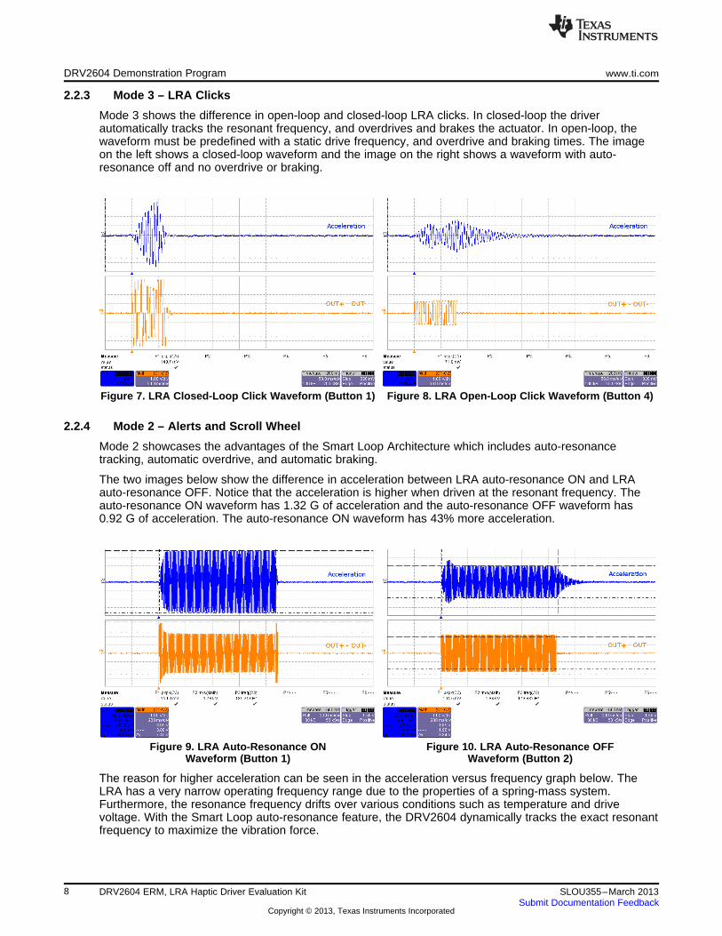
2.2.3 Mode 3 – LRA Clicks
Mode 3 shows the difference in open-loop and closed-loop LRA clicks. In closed-loop the driverautomatically tracks the resonant frequency, and overdrives and brakes the actuator. In open-loop, thewaveform must be predefined with a static drive frequency, and overdrive and braking times. The imageon the left shows a closed-loop waveform and the image on the right shows a waveform with auto-resonance off and no overdrive or braking.
Figure 7. LRA Closed-Loop Click Waveform (Button 1) Figure 8. LRA Open-Loop Click Waveform (Button 4)
2.2.4 Mode 2 – Alerts and Scroll Wheel
Mode 2 showcases the advantages of the Smart Loop Architecture which includes auto-resonancetracking, automatic overdrive, and automatic braking.
The two images below show the difference in acceleration between LRA auto-resonance ON and LRAauto-resonance OFF. Notice that the acceleration is higher when driven at the resonant frequency. Theauto-resonance ON waveform has 1.32 G of acceleration and the auto-resonance OFF waveform has0.92 G of acceleration. The auto-resonance ON waveform has 43% more acceleration.
Figure 9. LRA Auto-Resonance ON Figure 10. LRA Auto-Resonance OFFWaveform (Button 1) Waveform (Button 2)
The reason for higher acceleration can be seen in the acceleration versus frequency graph below. TheLRA has a very narrow operating frequency range due to the properties of a spring-mass system.Furthermore, the resonance frequency drifts over various conditions such as temperature and drivevoltage. With the Smart Loop auto-resonance feature, the DRV2604 dynamically tracks the exact resonantfrequency to maximize the vibration force.
8 DRV2604 ERM, LRA Haptic Driver Evaluation Kit SLOU355–March 2013Submit Documentation Feedback
Copyright © 2013, Texas Instruments Incorporated

www.ti.com DRV2604 Demonstration Program
Figure 11. Acceleration Versus Frequency
Button 4 uses a series of clicks to create a scroll wheel effect. See the oscilloscope capture in Figure 12.
Figure 12. LRA Scroll Wheel Effect Waveform (Button 4)
2.2.5 Mode 1 – Concentration Game
Mode 1 is a game that incorporates the various LRA and ERM effects. This can be used to demonstratehaptics in a real application.
To begin playing Concentration:
1. Press any of the large effect buttons.
2. The game then counts down.
3. Once the countdown completes, a button lights and an effect plays.
4. Repeat the pattern by pressing the same button.
5. After each successfully repeated pattern, the board repeats the same pattern and adds one additionalbutton effect to the sequence.
9SLOU355–March 2013 DRV2604 ERM, LRA Haptic Driver Evaluation KitSubmit Documentation Feedback
Copyright © 2013, Texas Instruments Incorporated

DRV2604 Demonstration Program www.ti.com
2.2.6 Mode 0 – Auto-Calibration
Auto-calibration is a DRV2604-embedded routine that detects the characteristics and behavior of anactuator and adjusts the drive waveform automatically.
Perform auto-calibration using the following steps:
1. Connect an actuator to the green output terminal (OUT) or use the on-board actuators
2. For an ERM actuator, run the ERM auto-calibration by pressing button B1
3. For an LRA actuator, run the LRA auto-calibration by pressing button B2
4. Read the auto-calibration register values using I2C
5. Test using buttons B3 and B4
2.3 RAM Library Mode
Access the RAM library effects by holding the + button until the mode LEDs flash and the colored LEDsflash ONCE.
Once in Library Mode the DRV2604 loaded RAM effects can be accessed in sequential order. Forexample, with all Mode LEDs off, B1 is waveform 1, B2 is waveform 2, and so on. Then when Mode LEDM0 is on, B1 is waveform 5, B2 is waveform 6, and so on.
The equations for calculating the Mode and Button of an effect are:Mode = RoundDown( [Effect No.] / 4 )Button = ([Effect No.] – 1) % 4 + 1% - modulo operator
To change between ERM and LRA:
1. Select mode 31 (11111'b) using the + or – buttons.
• B1 – Press to select ERM
• B2 – Press to select LRA
2. Then use the RAM effects as described above.
2.4 Waveform Library Effects List
Below is a description of the waveforms embedded in the DRV2604.
Effect ID Waveform Name
1 Strong Click
2 Medium Click
3 Light Click
4 Tick
5 Bump
6 Strong Double Click
7 Medium Double Click
8 Light Double Click
9 Strong Triple Click
10 Buzz
11 Ramp Up
12 Ramp Down
13 Click + Bounce
14 Ramp Up + Click
15 Gallop Alert
16 Pulsing Alert
10 DRV2604 ERM, LRA Haptic Driver Evaluation Kit SLOU355–March 2013Submit Documentation Feedback
Copyright © 2013, Texas Instruments Incorporated

www.ti.com Additional Hardware Modes
3 Additional Hardware Modes
Additional modes are available on the DRV2604EVM-CT providing increased board control andfunctionality. The additional modes are not available in demo mode, but can be accessed by switching tobinary counting mode. In binary counting mode the mode LEDs count in binary (32 modes) rather than indemo mode format (only 6 modes including off).
3.1 Enter Binary Counting Mode
To enter binary counting mode and access the additional modes:
1. Press and hold the increment mode button (+) for approximately 3 seconds until the mode LEDs flashand the colored LEDs flash once.
2. Press and hold the increment mode button (+) one more time until the mode LEDs flash and thecolored LEDs flash twice.
3. Select from the binary counting mode using the + and – buttons.
3.2 Exit Binary Counting Mode
To exit binary counting mode and return to demo mode:
1. Press and hold the decrement mode button (–) for approximately 3 seconds.
2. Release the button when the actuator buzzes and mode LEDs flash.
3. Select from the demo modes using the + and – buttons.
11SLOU355–March 2013 DRV2604 ERM, LRA Haptic Driver Evaluation KitSubmit Documentation Feedback
Copyright © 2013, Texas Instruments Incorporated

Additional Hardware Modes www.ti.com
3.3 Binary Counting Modes
Table 2 lists the modes available in binary counting mode.
Table 2. Binary Counting ModesMode Button Description Notes
Mode 0 B1 Set ERM Output Use this mode to control the DRV2604 using an external I2C Master. Press B1 or B2 tochoose between the ERM or LRA. Press B3 to choose the trigger type. (1 - Internal, 2 -External I2C Mode B2 Set LRA Output Ext. Edge, 3 - Ext. Level). Press B4 to trigger the waveform sequencer.LEDs: 00000
B3 Choose Trigger
B4 Trigger Button
Mode 1 B1 ERM Auto-Calibration Run the auto-calibration. The new auto-calibration results are used for all board effects.Auto-Calibration & 1 flash = successful, 3 flashes = error.
B2 LRA Auto-CalibrationDiagnosticsLEDs: 00001 B3 ERM Diagnostics Run diagnostics. 1 flash = successful, 3 flashes = error. The status register bits [3:0]
are displayed on the mode LEDs [3:0] when complete.B4 LRA Diagnostics
Mode 2 B1 Disable PWM Mode External PWM - disconnect MSP430 PWM using JP1. Connect external PWM signal toExternal PWM the "PWM" testpoint at the top of the board. Select actuator using buttons B2 and B3.
B2 Set ERM OutputLEDs: 00010B3 Set LRA Output
B4 -
Mode 3 B1 Return to normal mode External PWM and Enable - disconnect MSP430 PWM using JP1. Connect externalExternal PWM and Enable PWM signal to the "PWM" testpoint at the top of the board. Connect an external enable
B2 Set ERM OutputLEDs: 00011 signal to the "EN" testpoint. Select actuator using buttons B2 and B3. Press B1 beforeswitching modes.B3 Set LRA Output
B4 -
Mode 4 B1 AC Coupling - ERM Analog Input - apply an external analog signal for AC coupling on the "Audio" jack.Analog Input Apply a DC coupled signal to the "PWM" testpoint.
B2 DC Coupling - ERMLEDs: 00100B3 AC Coupling - LRA
B4 DC Coupling - LRA
Mode 5 B1 Alert (Auto-resonance On) Vary the auto-resonance OFF (open-loop) output frequency and see the change inAuto-resonance OFF vibration force over frequency. Hold B3 or B4 for quick frequency adjustment. Compare
B2 Alert (Auto-resonance Off)frequency adjust B2 (auto-resonance off) with B1 (auto-resonance on).LEDs: 00101 B3 Decrease output frequency
B4 Increase output frequency
Mode 6 B1 Begin Life Test Life Test using RTP (2 seconds on, 1 second off) - life test repeats infinite times andLife Test (RTP) 2s ON, 1s board must be powered down to stop. Increment / Decrement amplitude using B3 and
B2 Test BuzzOFF B4. Test new amplitude using B2. Choose actuator using buttons B1 and B2 in Mode 0LEDs: 00110 or Mode 1.B3 Decrease output voltage (–1)
B4 Increase output voltage (+1)
Mode 7 B1 Begin Life Test Life Test using RTP (Infinite Buzz) - board must be powered down to stop buzz.Life Test (RTP) Infinite Buzz Increment / Decrement amplitude using B3 and B4. Test new amplitude using B2
B2 Test BuzzLEDs: 00111 before beginning life test. Choose actuator using buttons B1 and B2 in Mode 0 orMode 1.B3 Decrease output voltage (–1)
B4 Increase output voltage (+1)
Mode 8 B1 Begin Life Test Life Test using PWM (2 seconds on, 1 second off) - life test repeats infinite times andLife Test (PWM) 2s ON, 1s board must be powered down to stop. Increment / Decrement amplitude using B3 and
B2 Test BuzzOFF B4. Test new amplitude using B2. Choose actuator using buttons B1 and B2 in Mode 0LEDs: 01000 or Mode 1.B3 Decrease output voltage (–1)
B4 Increase output voltage (+1)
Mode 9 B1 Start/Stop Recording Recorder - use this mode to create a single amplitude pattern. Start by pressing theRecorder record button (B1). Then use B2 to create the pattern by tapping the button. When
B2 Create PatternLEDs: 01001 finished press the play back button (B3).B3 Start/Stop Play Back
B4 -
Mode 10 B1 Life Test Infinite Buzz Life Test (RAM Mode) - Increment / Decrement amplitude using B3 and B4. B1 -Life Test (RAM) Infinite Buzz Start/Stop Infinite Buzz Life Test. B2 - Start/Stop 2s ON, 1s OFF life test. Choose
B2 Life Test 2s ON, 1s OFFLEDs: 01010 actuator using buttons B1 and B2 in Mode 0 or Mode 1.B3 Decrease output voltage (–1)
B4 Increase output voltage (+1)
Mode 30 B1 Begin Actuator Break-in Actuator Break-in - used to break in new actuatorsActuator Break-in
B2LEDs: 11110B3
B4
Mode 31 B1 Device ID About the Board - the value will appear on the mode LEDs in binary.About the Board DRV2604 Device ID = 00100
B2 Silicon RevisionLEDs: 11111B3 Code Revision
B4
12 DRV2604 ERM, LRA Haptic Driver Evaluation Kit SLOU355–March 2013Submit Documentation Feedback
Copyright © 2013, Texas Instruments Incorporated

US
B
VB
AT
MSP
DRV
USB
VBAT
USB
VBAT
www.ti.com Hardware Configuration
4 Hardware Configuration
The DRV2604EVM-CT is very flexible and can be used to completely evaluate the DRV2604. Thefollowing sections list the various hardware configurations.
4.1 Input and Output Overview
The DRV2604EVM-CT allows complete evaluation of the DRV2604 though test points, jacks, andconnectors. Table 3 gives a brief description of the hardware.
Table 3. Hardware Overview
Signal Description I/O
PWM External input to DRV2604 IN/TRIG pin Input/Observe
EN External DRV2604 enable control Input/Observe
Filtered output test points for observation, connect to oscilloscope orOUT+/OUT– Outputmeasurement equipment
OUT Unfiltered output terminal block, connect to actuator Output
USB USB power (5 V) Input
VBAT External Supply Power (2.5 V–5.5 V) Input
SBW MSP430 programming header Input/Output
I2C DRV2604 and MSP430 I2C bus Input/Output
The audio jack is connected to the IN/TRIG pin of the DRV2604. When theAudio DRV2604 is in analog input mode, an analog signal from this jack controls the Input
amplitude envelope of the output waveform.
Hardware configuration details can be found in the following sections.
4.2 Power Supply Selection
The DRV2604EVM-CT can be powered by USB or an external power supply (VBAT). Jumpers DRV andMSP are used to select USB or VBAT for the DRV2604 and MSP430G2553, respectively. See thefollowing table for possible configurations.
Figure 13. Power Jumper Selection
Supply Configuration DRV MSP DRV2604 Supply Voltage (1)
USB – Both USB USB 5 V
DRV2604 external supply, MSP430 VBAT USB VBATUSB
External supply – both VBAT VBAT VBAT
USB with 3.3-V LDO (2) – both USB USB 3.3 V (R4 = Short, R5 = Open)(1) The DRV2604 supply must be on before operating the MSP430.(2) If a 3.3-V DRV2604 supply voltage is preferred while using the USB as the power source, remove R5 and add a 0-Ω resistor
across R4.
13SLOU355–March 2013 DRV2604 ERM, LRA Haptic Driver Evaluation KitSubmit Documentation Feedback
Copyright © 2013, Texas Instruments Incorporated
JP1
VDD
DRV2604
EN
IN/TRIG GND
OUT+
OUT-
MSP430
PWM/GPIO
P3.1R8
EN PWM
SDA
SCL
SDA
SCL
C11
AUDIO R40, 0Q
R41, NP
SDA SCL
R43, 0Q
100k470pF
100k470pF
OUT
OUT- OUT+
From DRV2604
Hardware Configuration www.ti.com
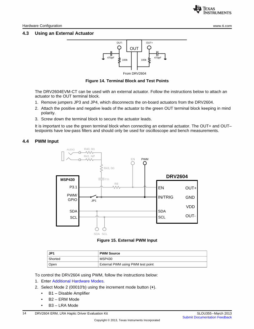
4.3 Using an External Actuator
Figure 14. Terminal Block and Test Points
The DRV2604EVM-CT can be used with an external actuator. Follow the instructions below to attach anactuator to the OUT terminal block.
1. Remove jumpers JP3 and JP4, which disconnects the on-board actuators from the DRV2604.
2. Attach the positive and negative leads of the actuator to the green OUT terminal block keeping in mindpolarity.
3. Screw down the terminal block to secure the actuator leads.
It is important to use the green terminal block when connecting an external actuator. The OUT+ and OUT–testpoints have low-pass filters and should only be used for oscilloscope and bench measurements.
4.4 PWM Input
Figure 15. External PWM Input
JP1 PWM Source
Shorted MSP430
Open External PWM using PWM test point
To control the DRV2604 using PWM, follow the instructions below:
1. Enter Additional Hardware Modes.
2. Select Mode 2 (00010'b) using the increment mode button (+).
• B1 – Disable Amplifier
• B2 – ERM Mode
• B3 – LRA Mode
14 DRV2604 ERM, LRA Haptic Driver Evaluation Kit SLOU355–March 2013Submit Documentation Feedback
Copyright © 2013, Texas Instruments Incorporated

JP1
VDD
DRV2604
EN
IN/TRIG GND
OUT+
OUT-
MSP430
PWM/GPIO
P3.1R8
EN PWM
SDA
SCL
SDA
SCL
C11
AUDIO R40, 0Q
R41, NP
SDA SCL
R43, 0Q
www.ti.com Hardware Configuration
• B4 – No function
3. Choose either the on-board ERM or LRA using buttons B1 or B2.
4. Apply the PWM signal to the PWM test point at the top of the board.
4.5 External Trigger Control
Figure 16. External Trigger Control
JP1 PWM Source
Shorted MSP430
Open External GPIO using PWM test point
The DRV2604 internal waveform sequencer can be triggered by controlling the IN/TRIG pin. There aretwo external trigger options: edge trigger and level trigger. See the data sheet for more information onthese Input Trigger Modes.
In Mode 0 in the Additional Hardware Modes section, the DRV2604 can be set in external trigger modeand then triggered by using the trigger button control on button B4 or alternatively by applying an externaltrigger signal to the PWM test point.
4.5.1 MSP430 Trigger Control1. Enter Additional Hardware Modes.
2. Select Mode 0 (00000’b) using the increment mode button (+).
• B1 – Select the on-board ERM
• B2 – Select the on-board LRA
• B3 – Trigger Select (1 = Internal Trigger, 2 = Ext. Edge, 3 = Ext. Level)
• B4 – Trigger the waveform sequence using the MSP430.
3. Fill the waveform sequencer with waveforms using the external I2C port.
4. Choose either the on-board ERM or LRA using buttons B1 or B2.
5. Select either External Edge (2) or External Level (3) trigger using the B3 button. The trigger typeappears in binary on the mode LEDs.
6. Apply the trigger signal to the IN/TRIG pin by pressing the B4 button.
15SLOU355–March 2013 DRV2604 ERM, LRA Haptic Driver Evaluation KitSubmit Documentation Feedback
Copyright © 2013, Texas Instruments Incorporated

JP1
VDD
DRV2604
EN
IN/TRIG GND
OUT+
OUT-
MSP430
PWM/GPIO
P3.1R8
EN PWM
SDA
SCL
SDA
SCL
C11
AUDIO R40, 0Q
R41, NP
SDA SCL
R43, 0Q
Hardware Configuration www.ti.com
4.5.2 External Source Trigger Control1. Remove jumper JP1.
2. Enter Additional Hardware Modes.
3. Select Mode 0 (00000’b) using the increment mode button (+).
• B1 – Select the on-board ERM
• B2 – Select the on-board LRA
• B3 – Trigger Select (1 = Internal Trigger, 2 = Ext. Edge, 3 = Ext. Level)
• B4 – Trigger the waveform sequence using the MSP430.
4. Fill the waveform sequencer with waveforms using the external I2C port.
5. Choose either the on-board ERM or LRA using buttons B1 or B2.
6. Select either External Edge (2) or External Level (3) trigger using the B3 button. The trigger typeappears in binary on the mode LEDs.
7. Apply the external logic signal to the PWM test point to trigger the waveform.
4.6 External I2C Input
Figure 17. External I2C Input
The DV2604 can be controlled by an external I2C source. Attach the external controller to the I2C headerat the top of the board; be sure to connect SDA, SCL and GND from the external source.
I2C communication is possible only when the EN pin is set high. To enable the DRV2604 and allowexternal I2C control, follow the instructions below.
1. Enter Additional Hardware Modes.
2. Select Mode 0 (00000’b) using the increment mode button (+).
• B1 – Select the on-board ERM
• B2 – Select the on-board LRA
• B3 – Trigger Select (1 = Internal Trigger, 2 = Ext. Edge, 3 = Ext. Level)
• B4 – Trigger the waveform sequence using the MSP430.
3. Choose either the on-board ERM or LRA using buttons B1 or B2. Either button sets the EN pin highand turns on the Active LED.
4. Begin controlling the DRV2604 using the external I2C source.
16 DRV2604 ERM, LRA Haptic Driver Evaluation Kit SLOU355–March 2013Submit Documentation Feedback
Copyright © 2013, Texas Instruments Incorporated

100k470pF
100k470pF
OUT
OUT- OUT+
From DRV2604
JP1
VDD
DRV2604
EN
IN/TRIG GND
OUT+
OUT-
MSP430
PWM/GPIO
P3.1R8
EN PWM
SDA
SCL
SDA
SCL
C11
AUDIO R40, 0Q
R41, NP
SDA SCL
R43, 0Q
www.ti.com Measurement and Analysis
4.7 Analog Input
Figure 18. Analog Input
The analog input accepts an analog signal to control the envelope of the output waveform.
Use the following steps to use analog input mode:
1. Apply an analog signal (not PWM) to the AUDIO jack on the left side of the board. The tip of theinserted male 3.5 mm jack is applied to the IN/TRIG pin of the DRV2604. See Figure 18.
2. Enter Additional Hardware Modes.
3. Select Mode 5 (00101’b) using the increment mode button (+).
4. In Mode 5, choose button B1–B4, depending on the actuator and input coupling.
• B1 – AC Coupling – ERM
• B2 – DC Coupling – ERM
• B3 – AC Coupling – LRA
• B4 – DC Coupling – LRA
5. Enable the analog input signal.
5 Measurement and Analysis
The DRV2604 uses PWM modulation to create the output signal for both ERM and LRA actuators. Tomeasure and observe the DRV2604 output waveform, connect an oscilloscope or other measurementequipment to the filtered output test points, OUT+ and OUT–.
Figure 19. Terminal Block and Test Points
17SLOU355–March 2013 DRV2604 ERM, LRA Haptic Driver Evaluation KitSubmit Documentation Feedback
Copyright © 2013, Texas Instruments Incorporated

ERMOr
LRA
OUT+
OUT-
100k
100k
470 pF
470 pF
Ch1-Ch2(Differential )
Oscilloscope
Ch1
Ch2
Measurement and Analysis www.ti.com
The DRV2604 drives LRA and ERM actuators using a 20-kHz PWM modulated waveform, but only thefrequencies around the LRA resonant frequency or the ERM DC drive voltage are relevant to the hapticactuator vibration. The higher frequency switching content does not contribute to the vibration strength ofthe actuator and can make it difficult to interpret the modulated output waveform on an oscilloscope. Theoscilloscope image on the left shows the DRV2604 unfiltered waveform and the image on the right showsa filtered version used for observation and measurement.
Figure 20. DRV2604 Unfiltered Waveform Figure 21. DRV2604 Filtered Waveform
If the DRV2604EVM-CT filter is not used, TI recommends using a 1st-order, low-pass filter with a cutoffbetween 1kHz and 3.5kHz . Below is a recommended output filter for use while measuring andcharacterizing the DRV2604 in the lab.
Figure 22. Measuring the DRV2604 Output Signal with an Analog Low-Pass Filter
18 DRV2604 ERM, LRA Haptic Driver Evaluation Kit SLOU355–March 2013Submit Documentation Feedback
Copyright © 2013, Texas Instruments Incorporated

www.ti.com Modifying or Reprogramming the Firmware
6 Modifying or Reprogramming the Firmware
The MSP430 firmware on the DRV2604EVM-CT can be modified or reprogrammed to create new hapticeffects or behaviors. Find the latest firmware source code and binaries on ti.com. Follow the instructionsbelow to modify or reprogram the DRV2604EVM-CT.
1. Purchase one of the following MSP430G2553 compatible programmers:
• LaunchPad (MSP-EXP430G2) – requires the additional purchase of a header for J4(recommended)
– Digi-Key: ED8650-ND
– Mouser: 575-500201
• MSP430-FET430UIF – requires a JTAG to Spy-Bi-Wire adapter (MSP-JTAGSBW if available)
2. Download and install Code Compose Studio (CCS) or IAR Embedded Workbench IDE.
3. Download the DRV2604EVM-CT source code and binaries from ti.com.
4. Connect the programmer to an available USB port.
5. Connect the programmer to the SBW header on the DRV2604EVM-CT.
6. In CCS,
(a) Open the project file by selecting Project→Import Existing CCS Project.
(b) Select Browse and navigate to the DRV2604EVM-CT project folder, then press OK.
(c) Select the checkbox next to the DRV2604EVM-CT project in the Discovered projects window andthen press Finish.
(d) Before compiling, navigate to Project→Properties→Build→MSP430 Compiler→AdvancedOptions→Language Options and make sure the checkbox for Enable support for GCC extensions(–gcc) is checked.
7. In IAR,
(a) Create a new MSP430 project in IAR,
(b) Select the MSP430G2553 device,
(c) Copy the files in the project folder downloaded from ti.com to the new project directory.
The figure below shows the connection between the MSP430 LaunchPad (MSP-EXP430G2) and theDRV2604EVM-CT.
Figure 23. LaunchPad Programmer Connection
19SLOU355–March 2013 DRV2604 ERM, LRA Haptic Driver Evaluation KitSubmit Documentation Feedback
Copyright © 2013, Texas Instruments Incorporated

Modifying or Reprogramming the Firmware www.ti.com
6.1 MSP430 Pin-Out
The DRV2604EVM-CT contains a MSP430G2553 low-cost microcontroller which controls the board andcontains sample haptic effects. The pin-out for the microcontroller is found in Table 4.
Table 4. MSP430 Pin-Out
# Label Description
1 P1.1 Green LED
2 P1.2 Yellow LED
3 P1.3 Blue LED
4 P1.4 VREF+
5 P1.5 Audio-to-Haptics
6 P3.1 Enable
7 P3.0 Actuator Mode Selection
8 NC
9 P2.0 Button 1
10 P2.1 Button 2
11 P2.2 Button 3
12 P3.2 PWM
13 P3.3 WLED 0
14 P3.4 WLED 1
15 P2.3 Button 4
16 P2.4 + Button
17 P2.5 – Button
18 P3.5 WLED 2
19 P3.6 WLED 3
20 P3.7 WLED 4
21 P1.6/SCL I2C Clock
22 P1.7/SDA I2C Data
23 SBWTDIO Spy-Bi-Wire Data
24 SBWTCK Spy-Bi-Wire Clock
25 P2.7
26 P2.6 LRA/ERM Load Switch
27 AVSS Analog Ground
28 DVSS Digital Ground
29 AVCC Analog Supply
30 DVCC Digital Supply
31 P1.0 Red LED
32 NC
20 DRV2604 ERM, LRA Haptic Driver Evaluation Kit SLOU355–March 2013Submit Documentation Feedback
Copyright © 2013, Texas Instruments Incorporated

SDA
SCL
SBWTDIO
WL
ED
3
SCL-IN
WLED3
WLED4
BTN5
WLED2
BT
N4
BT
N3
WL
ED
0
WL
ED
1
WL
ED
2
WL
ED
1
BT
N2
BT
N1
BT
N0
BT
N5
BT
N4
BT
N3
BT
N2
BT
N1
BT
N0
Audio2Haptics
SCL
SDA
SDA-IN
WL
ED
4
WL
ED
0
Lo
ad
Sw
itch
LoadSwitch
SBW
GND
Vbat
GND
GND
Black
GND
GND
+3.3V
GND
+3.3V
9.76K0402
R7
+3.3V
0.1ufd/6.3V0402
C10
10ufd/16V0805
C6
GND
1.0ufd/6.3V0402
C7
GND
6A/125VGreen
VBAT
+3.3V
SSOP8-DCT
U4TXS0102DCT
GND
0.1ufd/6.3V0402
C9
GND
R8
0.00402
100ufd/6.3VTCT-TANT1206
C5+
GND
I2C
GND
GND
Green0603
ACTIVE
JP2+3.3V
0.1ufd/6.3V0402
C8
R95110402
JP1
GND
GNDOrangeENIN
OrangePWM
GND
R13
0402511
GND
R115110402 GND
R125110402
GND
R145110402
GND
M3
0603White
GND
M2
0603White
GND
M1
0603White
GND
M0
0603White
BlackTP1
GND
B1
Red0805
B2
Green0805
B3
Yellow0805
B40805Blue
GND
5V
0603Green
GND
04021.5KR26
USB
USB MINIB
FB1
600 Ohms/2A
0805
FB2
600 Ohms/2A
0805
0402DNPR20
DNP0402
R21
0402DNPR22
DNP0402
R23
0402DNP
R24DNP0402
R25
GND
+5V-USB
DRV
MSP
GND
Green6A/125V
OUT
C1
04020.1ufd/16V
GND
Vbat
+5V-USB
R5
06030.0
R4
DNP0603
R16
0402249 249
0402
R17
0402249R18
2490402
R19
TPS73633DBV3.3V/400mA
U3
GND
White0603
M4
2490402
R15
WCSP6-YFP
U5
TS5A12301EYFPR
GNDLRA_OUT+
LRA_OUT-
JP3
0402DNP
R31
DNP0402
R30
04020.0
R32
Vbat
0.1ufd/16V0402
C12
GND
3.5mmSJ-3523-SMT
Audio
GND
0.1ufd/10V0603 X7R
C11
0.00402
R40
DNP0402
R41
DNP0402
R42
GND
0.00402
R33
JP4
U2
QFN32-RHB
GND
AVM1
-
+R34
0.00402
R35
0402DNP
Vbat
R36
04020.0
GND
0.1ufd/16V0402
C2
GND
WCSP9-YZF
U1
IN/TRIG
EN
SDA
VR
EG
OUT-
OUT+
SCL
VB
AT
GN
D
MSP430G2553RHB
U2
QFN32-RHB
P2.5
P3.5
P3.7
P1.6/SCL
P1.7/SDA
P3.6
SBWTDIO
SBWTCK P1.0
NC
DV
SS
AV
SS
DV
CC
P2.7
P2.6
AV
CC
P1.1
P3.1
P1.5
P3.0
P1.4
P1.2
P1.3
NC
P2.0
P2.1
P3.2
P2.2
P2.3
P2.4
P3.4
P3.3
R43
04020.0
OUT+Orange
R50
100K/5%0402 C14
0402 X7R470pfd/50V
GND
OUT-Orange
R51
100K/5%0402 C15
0402 X7R470pfd/50V
GND
SBYBIWIRE
Audio-to-Haptics
MSP / DRV1-2: VBAT POWER2-3: USB POWER
DRV2604
MODE SELECT LEDS
3.6V - 5.5VPOWERSUPPLY
USB POWER
EXT INPUT
DRV2604YZF CAPTOUCH EVM
CAPTOUCH RESISTORS
ERM/LRA ACTUATORSWITCH
ERM
LRA
www.ti.com Schematic
7 Schematic
Figure 24. DRV2604EVM-CT Schematic
21SLOU355–March 2013 DRV2604 ERM, LRA Haptic Driver Evaluation KitSubmit Documentation Feedback
Copyright © 2013, Texas Instruments Incorporated

Layout www.ti.com
8 Layout
Figure 25. X-Ray Top View
spacer
Figure 26. Top Copper
22 DRV2604 ERM, LRA Haptic Driver Evaluation Kit SLOU355–March 2013Submit Documentation Feedback
Copyright © 2013, Texas Instruments Incorporated

www.ti.com Layout
Figure 27. Layer 2 Copper
spacer
Figure 28. Layer 3 Copper
23SLOU355–March 2013 DRV2604 ERM, LRA Haptic Driver Evaluation KitSubmit Documentation Feedback
Copyright © 2013, Texas Instruments Incorporated

Layout www.ti.com
Figure 29. Bottom Copper
24 DRV2604 ERM, LRA Haptic Driver Evaluation Kit SLOU355–March 2013Submit Documentation Feedback
Copyright © 2013, Texas Instruments Incorporated

www.ti.com Bill of Materials
9 Bill of Materials
ITEM MANU PARTNUM QTY REF DESIGNATORS VENDOR PARTNUM DESCRIPTION MANUFACTURER
SEMICONDUCTORS
1 DRV2604YZF 1 U1 DRV2604YZF HAPTIC DRIVER AUTO DETECT FOR TEXAS INSTRUMENTSLRA AND ERM WCSP9-YZF ROHS
2 TXS0102DCTR 1 U4 296-21978-1 2-BIT BIDIR LEVEL TRANSLATOR TEXAS INSTRUMENTSSSOP8-DCT ROHS
3 MSP430G2553IRHB32T 1 U2 595-P430G2553IRHB32T MIXED SIGNAL MICRO 16KB FLASH TEXAS INSTRUMENTS512B RAM QFN32-RHB ROHS
4 TPS73633MDBVREP 1 U3 296-21283-1 VOLT REG 3.3V 400MA LDO CAP TEXAS INSTRUMENTSFREE NMOS SOT23-DBV5 ROHS
5 TS5A12301EYFPR 1 U5 296-23757-1-ND IEC LEVEL 4 ESD-PROTECTED 0.75- TEXAS INSTRUMENTSOHM ANALOG SWITCH WCSP6-YFPROHS
6 LTST-C190KGKT 2 5V,ACTIVE 160-1435-1-ND LED,GREEN,2.0V,SMD0603,ROHS LITE-ON INC.
7 LNJ037X8ARA 5 M0,M1,M2,M3,M4 LNJ037X8ARACT-ND LED, WHITE 2.9V SMD0805 ROHS PANASONIC
8 SML-LXT0805SRW-TR 1 B1 67-1555-1 LED, RED 2.0V SMD0805 ROHS LUMEX OPTO
9 SML-LXT0805GW-TR 1 B2 67-1553-1 LED, GREEN 2.0V SMD0805 ROHS LUMEX OPTO
10 SML-LXT0805YW-TR 1 B3 67-1554-1 LED, YELLOW 2.0V SMD0805 ROHS LUMEX OPTO
11 LTST-C171TBKT 1 B4 160-1645-1-ND LED, BLUE 3.3V SMD0805 ROHS LITE-ON INC.
CAPACITORS
12 GRM155R71C104KA88D 3 C1,C2,C12 490-3261-1-ND CAP SMD0402 CERM 0.1UFD 16V MURATAX7R 10% ROHS
13 C1005X5R0J104K 3 C8,C9,C10 445-1266-1 CAP SMD0402 CERM 0.1UFD 6.3V TDK CORP10% X5R ROHS
14 0805YD106KAT2A 1 C6 478-5165-1 CAP SMD0805 CERM 10UFD 16V AVXX5R 10% ROHS
15 GRM155R60J105KE19D 1 C7 490-1320-1 CAP SMD0402 CERM 1.0UFD 6.3V MURATAX5R 10% ROHS
16 C1005X5R0J104K 1 C11 445-1266-1 CAP SMD0402 CERM 0.1UFD 6.3V TDK CORP10% X5R ROHS
17 C0402C471K5RACTU 2 C14,C15 399-1025-1 CAP SMD0402 CERM 470PFD 50V KEMET10% X7R ROHS
18 TCTAL0J107M8R 1 C5 511-1498-1-ND CAP TANT1206 100UFD 6.3V 20% ROHMTCT SERIES ROHS
RESISTORS
19 ERJ-2RKF9761X 1 R7 P9.76KLCT-ND RESISTOR SMD0402 THICK FILM PANASONIC9.76K OHMS 1/10W 1% ROHS
20 RMCF0402ZT0R00 5 R8,R32,R33,R34,R36 RMCF0402ZT0R00CT ZERO OHM JUMPER SMT 0402 0 STACKPOLE ELECTRONICSOHM 1/16W,5% ROHS
25SLOU355–March 2013 DRV2604 ERM, LRA Haptic Driver Evaluation KitSubmit Documentation Feedback
Copyright © 2013, Texas Instruments Incorporated

Bill of Materials www.ti.com
ITEM MANU PARTNUM QTY REF DESIGNATORS VENDOR PARTNUM DESCRIPTION MANUFACTURER
21 RC0402FR-07511RL 5 R9,R11,R12,R13,R14 311-511LRCT-ND RESISTOR SMD0402 THICK FILM YAGEO511 OHMS 1% 1/16W ROHS
22 ERJ-2GEJ152 1 R26 RESISTOR,SMT,0402,THICK PanasonicFILM,5%,1/16W,1.5K
23 RMCF0603ZT0R00 1 R5 RMCF0603ZT0R00CT- RESISTOR SMD0603 ZERO OHMS STACKPOLE ELECTRONICSND 1/10W ROHS
24 ERJ-2RKF2490X 5 R15,R16,R17,R18,R19 P249LTR-ND RESISTOR,SMT,0402,249 PanasonicOHM,1%,1/16W
25 CRCW04020000Z0ED 2 R40,R43 541-0.0JCT ZERO OHM JUMPER SMT 0402 0 VISHAYOHM 1/16W,5% ROHS
26 ERJ-2GEJ104 2 R50,R51 P100KJCT RESISTOR SMD0402 THICK FILM PANASONIC100K OHMS 1/16W 5% ROHS
FERRITE BEADS
27 MPZ2012S601A 2 FB1,FB2 445-2206-1 FERRITE BEAD SMD0805 600 Ohms TDK2A ROHS
HEADERS, JACKS, AND SHUNTS
28 LPPB061NGCN-RC 1 SBW S9010E-06 HEADER THRU FEMALE 1X6-RA SULLINS50LS GOLD ROHS
29 PBC03SAAN 3 DRV,I2C,MSP S1011E-03-ND HEADER THRU MALE 3 PIN 100LS SULLINSGOLD ROHS
30 PBC02SAAN 1 JP2 S1011E-02 HEADER THRU MALE 2 PIN 100LS SULLINSGOLD ROHS
31 PBC02SAAN 3 JP1,JP3,JP4 HEADER THRU MALE 2 PIN 100LS SULLINSGOLD ROHS
32 UX60-MB-5ST 1 USB H2959CT JACK USB MINIB SMT-RA 5PIN HIROSEROHS
33 SJ-3523-SMT 1 Audio CP-3523SJCT-ND JACK AUDIO-STEREO MINI(3.5MM CUI STACK,3-COND SMT-RA ROHS
34 SPC02SYAN 6 MSP (2-3), DRV (2-3), S9001-ND SHUNT BLACK AU FLASH 0.100LS SULLINSJP1, JP2, JP3, JP4 CLOSED TOP ROHS
35 1725656 2 OUT,VBAT 277-1273 TERMINAL BLOCK MPT COMBICON PHOENIX CONTACT2PIN 6A/125V GREEN 100LS ROHS
TESTPOINTS AND SWITCHES
36 5011 2 GND,TP1 ((Solder so 5011K PC TESTPOINT BLACK 063 HOLE KEYSTONE ELECTRONICSthat color ring is secured) ROHS
37 5003 4 PWM,ENIN, OUT+, 5003K PC TESTPOINT, ORANGE, ROHS KEYSTONE ELECTRONICSOUT– (Solder so thatcolor ring is secured)
26 DRV2604 ERM, LRA Haptic Driver Evaluation Kit SLOU355–March 2013Submit Documentation Feedback
Copyright © 2013, Texas Instruments Incorporated

www.ti.com Bill of Materials
ITEM MANU PARTNUM QTY REF DESIGNATORS VENDOR PARTNUM DESCRIPTION MANUFACTURER
38 NRS-2574 1 AVM1 NRS-2574 ACTUATOR VIBRATION MOTOR 1,3V SANYO9000 RPM ROHS
39 ELV1036A 1 - - ACTUATOR - LINEAR VIBRATOR, AAC2VRMS
40 - 1 - - Metal Block (Custom Block, Heavy Heavy MetalMetal, See metal block spec)
41 3-5-468MP 1 - 3M9724-ND TAPE TRANSFER ADHESIVE 3" X 3M5YD
42 2-5-4466W 1 - 3M9962-ND TAPE POLY FOAM 2" x 5YD 3M
COMPONENTS NOT ASSEMBLED
43 TestPoint_SMD- 2 LRA_OUT+, LRA_OUT– TESTPOINT SMD SQUARE 2.0mmSquare_2.0mm
44 R0402_DNP 9 R20,R21,R22,R23,R24,R R0402_DNP25,R30,R31,R35
45 R0603_DNP 1 R4 RMCF0603ZT0R00CT- R0603_DNP STACKPOLE ELECTRONICSND
46 R0402_DNP 1 R41 P4.99KLCT-ND R0402_DNP PANASONIC
47 R0402_DNP 1 R42 541-0.0JCT R0402_DNP VISHAY
27SLOU355–March 2013 DRV2604 ERM, LRA Haptic Driver Evaluation KitSubmit Documentation Feedback
Copyright © 2013, Texas Instruments Incorporated

EVALUATION BOARD/KIT/MODULE (EVM) ADDITIONAL TERMS
Texas Instruments (TI) provides the enclosed Evaluation Board/Kit/Module (EVM) under the following conditions:
The user assumes all responsibility and liability for proper and safe handling of the goods. Further, the user indemnifies TI from all claimsarising from the handling or use of the goods.
Should this evaluation board/kit not meet the specifications indicated in the User’s Guide, the board/kit may be returned within 30 days fromthe date of delivery for a full refund. THE FOREGOING LIMITED WARRANTY IS THE EXCLUSIVE WARRANTY MADE BY SELLER TOBUYER AND IS IN LIEU OF ALL OTHER WARRANTIES, EXPRESSED, IMPLIED, OR STATUTORY, INCLUDING ANY WARRANTY OFMERCHANTABILITY OR FITNESS FOR ANY PARTICULAR PURPOSE. EXCEPT TO THE EXTENT OF THE INDEMNITY SET FORTHABOVE, NEITHER PARTY SHALL BE LIABLE TO THE OTHER FOR ANY INDIRECT, SPECIAL, INCIDENTAL, OR CONSEQUENTIALDAMAGES.
Please read the User's Guide and, specifically, the Warnings and Restrictions notice in the User's Guide prior to handling the product. Thisnotice contains important safety information about temperatures and voltages. For additional information on TI's environmental and/or safetyprograms, please visit www.ti.com/esh or contact TI.
No license is granted under any patent right or other intellectual property right of TI covering or relating to any machine, process, orcombination in which such TI products or services might be or are used. TI currently deals with a variety of customers for products, andtherefore our arrangement with the user is not exclusive. TI assumes no liability for applications assistance, customer product design,software performance, or infringement of patents or services described herein.
REGULATORY COMPLIANCE INFORMATION
As noted in the EVM User’s Guide and/or EVM itself, this EVM and/or accompanying hardware may or may not be subject to the FederalCommunications Commission (FCC) and Industry Canada (IC) rules.
For EVMs not subject to the above rules, this evaluation board/kit/module is intended for use for ENGINEERING DEVELOPMENT,DEMONSTRATION OR EVALUATION PURPOSES ONLY and is not considered by TI to be a finished end product fit for general consumeruse. It generates, uses, and can radiate radio frequency energy and has not been tested for compliance with the limits of computingdevices pursuant to part 15 of FCC or ICES-003 rules, which are designed to provide reasonable protection against radio frequencyinterference. Operation of the equipment may cause interference with radio communications, in which case the user at his own expense willbe required to take whatever measures may be required to correct this interference.
General Statement for EVMs including a radio
User Power/Frequency Use Obligations: This radio is intended for development/professional use only in legally allocated frequency andpower limits. Any use of radio frequencies and/or power availability of this EVM and its development application(s) must comply with locallaws governing radio spectrum allocation and power limits for this evaluation module. It is the user’s sole responsibility to only operate thisradio in legally acceptable frequency space and within legally mandated power limitations. Any exceptions to this are strictly prohibited andunauthorized by Texas Instruments unless user has obtained appropriate experimental/development licenses from local regulatoryauthorities, which is responsibility of user including its acceptable authorization.
For EVMs annotated as FCC – FEDERAL COMMUNICATIONS COMMISSION Part 15 Compliant
Caution
This device complies with part 15 of the FCC Rules. Operation is subject to the following two conditions: (1) This device may not causeharmful interference, and (2) this device must accept any interference received, including interference that may cause undesired operation.
Changes or modifications not expressly approved by the party responsible for compliance could void the user's authority to operate theequipment.
FCC Interference Statement for Class A EVM devices
This equipment has been tested and found to comply with the limits for a Class A digital device, pursuant to part 15 of the FCC Rules.These limits are designed to provide reasonable protection against harmful interference when the equipment is operated in a commercialenvironment. This equipment generates, uses, and can radiate radio frequency energy and, if not installed and used in accordance with theinstruction manual, may cause harmful interference to radio communications. Operation of this equipment in a residential area is likely tocause harmful interference in which case the user will be required to correct the interference at his own expense.

FCC Interference Statement for Class B EVM devices
This equipment has been tested and found to comply with the limits for a Class B digital device, pursuant to part 15 of the FCC Rules.These limits are designed to provide reasonable protection against harmful interference in a residential installation. This equipmentgenerates, uses and can radiate radio frequency energy and, if not installed and used in accordance with the instructions, may causeharmful interference to radio communications. However, there is no guarantee that interference will not occur in a particular installation. Ifthis equipment does cause harmful interference to radio or television reception, which can be determined by turning the equipment off andon, the user is encouraged to try to correct the interference by one or more of the following measures:
• Reorient or relocate the receiving antenna.• Increase the separation between the equipment and receiver.• Connect the equipment into an outlet on a circuit different from that to which the receiver is connected.• Consult the dealer or an experienced radio/TV technician for help.
For EVMs annotated as IC – INDUSTRY CANADA Compliant
This Class A or B digital apparatus complies with Canadian ICES-003.
Changes or modifications not expressly approved by the party responsible for compliance could void the user’s authority to operate theequipment.
Concerning EVMs including radio transmitters
This device complies with Industry Canada licence-exempt RSS standard(s). Operation is subject to the following two conditions: (1) thisdevice may not cause interference, and (2) this device must accept any interference, including interference that may cause undesiredoperation of the device.
Concerning EVMs including detachable antennas
Under Industry Canada regulations, this radio transmitter may only operate using an antenna of a type and maximum (or lesser) gainapproved for the transmitter by Industry Canada. To reduce potential radio interference to other users, the antenna type and its gain shouldbe so chosen that the equivalent isotropically radiated power (e.i.r.p.) is not more than that necessary for successful communication.
This radio transmitter has been approved by Industry Canada to operate with the antenna types listed in the user guide with the maximumpermissible gain and required antenna impedance for each antenna type indicated. Antenna types not included in this list, having a gaingreater than the maximum gain indicated for that type, are strictly prohibited for use with this device.
Cet appareil numérique de la classe A ou B est conforme à la norme NMB-003 du Canada.
Les changements ou les modifications pas expressément approuvés par la partie responsable de la conformité ont pu vider l’autorité del'utilisateur pour actionner l'équipement.
Concernant les EVMs avec appareils radio
Le présent appareil est conforme aux CNR d'Industrie Canada applicables aux appareils radio exempts de licence. L'exploitation estautorisée aux deux conditions suivantes : (1) l'appareil ne doit pas produire de brouillage, et (2) l'utilisateur de l'appareil doit accepter toutbrouillage radioélectrique subi, même si le brouillage est susceptible d'en compromettre le fonctionnement.
Concernant les EVMs avec antennes détachables
Conformément à la réglementation d'Industrie Canada, le présent émetteur radio peut fonctionner avec une antenne d'un type et d'un gainmaximal (ou inférieur) approuvé pour l'émetteur par Industrie Canada. Dans le but de réduire les risques de brouillage radioélectrique àl'intention des autres utilisateurs, il faut choisir le type d'antenne et son gain de sorte que la puissance isotrope rayonnée équivalente(p.i.r.e.) ne dépasse pas l'intensité nécessaire à l'établissement d'une communication satisfaisante.
Le présent émetteur radio a été approuvé par Industrie Canada pour fonctionner avec les types d'antenne énumérés dans le manueld’usage et ayant un gain admissible maximal et l'impédance requise pour chaque type d'antenne. Les types d'antenne non inclus danscette liste, ou dont le gain est supérieur au gain maximal indiqué, sont strictement interdits pour l'exploitation de l'émetteur.
SPACER
SPACER
SPACER
SPACER
SPACER
SPACER
SPACER
SPACER

【【Important Notice for Users of this Product in Japan】】This development kit is NOT certified as Confirming to Technical Regulations of Radio Law of Japan
If you use this product in Japan, you are required by Radio Law of Japan to follow the instructions below with respect to this product:
1. Use this product in a shielded room or any other test facility as defined in the notification #173 issued by Ministry of Internal Affairs andCommunications on March 28, 2006, based on Sub-section 1.1 of Article 6 of the Ministry’s Rule for Enforcement of Radio Law ofJapan,
2. Use this product only after you obtained the license of Test Radio Station as provided in Radio Law of Japan with respect to thisproduct, or
3. Use of this product only after you obtained the Technical Regulations Conformity Certification as provided in Radio Law of Japan withrespect to this product. Also, please do not transfer this product, unless you give the same notice above to the transferee. Please notethat if you could not follow the instructions above, you will be subject to penalties of Radio Law of Japan.
Texas Instruments Japan Limited(address) 24-1, Nishi-Shinjuku 6 chome, Shinjuku-ku, Tokyo, Japan
http://www.tij.co.jp
【ご使用にあたっての注】
本開発キットは技術基準適合証明を受けておりません。
本製品のご使用に際しては、電波法遵守のため、以下のいずれかの措置を取っていただく必要がありますのでご注意ください。1. 電波法施行規則第6条第1項第1号に基づく平成18年3月28日総務省告示第173号で定められた電波暗室等の試験設備でご使用いただく。2. 実験局の免許を取得後ご使用いただく。3. 技術基準適合証明を取得後ご使用いただく。
なお、本製品は、上記の「ご使用にあたっての注意」を譲渡先、移転先に通知しない限り、譲渡、移転できないものとします。
上記を遵守頂けない場合は、電波法の罰則が適用される可能性があることをご留意ください。
日本テキサス・インスツルメンツ株式会社東京都新宿区西新宿6丁目24番1号西新宿三井ビルhttp://www.tij.co.jp
SPACER
SPACER
SPACER
SPACER
SPACER
SPACER
SPACER
SPACER
SPACER
SPACER
SPACER
SPACER
SPACER
SPACER
SPACER
SPACER
SPACER

EVALUATION BOARD/KIT/MODULE (EVM)WARNINGS, RESTRICTIONS AND DISCLAIMERS
For Feasibility Evaluation Only, in Laboratory/Development Environments. Unless otherwise indicated, this EVM is not a finishedelectrical equipment and not intended for consumer use. It is intended solely for use for preliminary feasibility evaluation inlaboratory/development environments by technically qualified electronics experts who are familiar with the dangers and application risksassociated with handling electrical mechanical components, systems and subsystems. It should not be used as all or part of a finished endproduct.
Your Sole Responsibility and Risk. You acknowledge, represent and agree that:
1. You have unique knowledge concerning Federal, State and local regulatory requirements (including but not limited to Food and DrugAdministration regulations, if applicable) which relate to your products and which relate to your use (and/or that of your employees,affiliates, contractors or designees) of the EVM for evaluation, testing and other purposes.
2. You have full and exclusive responsibility to assure the safety and compliance of your products with all such laws and other applicableregulatory requirements, and also to assure the safety of any activities to be conducted by you and/or your employees, affiliates,contractors or designees, using the EVM. Further, you are responsible to assure that any interfaces (electronic and/or mechanical)between the EVM and any human body are designed with suitable isolation and means to safely limit accessible leakage currents tominimize the risk of electrical shock hazard.
3. You will employ reasonable safeguards to ensure that your use of the EVM will not result in any property damage, injury or death, evenif the EVM should fail to perform as described or expected.
4. You will take care of proper disposal and recycling of the EVM’s electronic components and packing materials.
Certain Instructions. It is important to operate this EVM within TI’s recommended specifications and environmental considerations per theuser guidelines. Exceeding the specified EVM ratings (including but not limited to input and output voltage, current, power, andenvironmental ranges) may cause property damage, personal injury or death. If there are questions concerning these ratings please contacta TI field representative prior to connecting interface electronics including input power and intended loads. Any loads applied outside of thespecified output range may result in unintended and/or inaccurate operation and/or possible permanent damage to the EVM and/orinterface electronics. Please consult the EVM User's Guide prior to connecting any load to the EVM output. If there is uncertainty as to theload specification, please contact a TI field representative. During normal operation, some circuit components may have case temperaturesgreater than 60°C as long as the input and output are maintained at a normal ambient operating temperature. These components includebut are not limited to linear regulators, switching transistors, pass transistors, and current sense resistors which can be identified using theEVM schematic located in the EVM User's Guide. When placing measurement probes near these devices during normal operation, pleasebe aware that these devices may be very warm to the touch. As with all electronic evaluation tools, only qualified personnel knowledgeablein electronic measurement and diagnostics normally found in development environments should use these EVMs.
Agreement to Defend, Indemnify and Hold Harmless. You agree to defend, indemnify and hold TI, its licensors and their representativesharmless from and against any and all claims, damages, losses, expenses, costs and liabilities (collectively, "Claims") arising out of or inconnection with any use of the EVM that is not in accordance with the terms of the agreement. This obligation shall apply whether Claimsarise under law of tort or contract or any other legal theory, and even if the EVM fails to perform as described or expected.
Safety-Critical or Life-Critical Applications. If you intend to evaluate the components for possible use in safety critical applications (suchas life support) where a failure of the TI product would reasonably be expected to cause severe personal injury or death, such as deviceswhich are classified as FDA Class III or similar classification, then you must specifically notify TI of such intent and enter into a separateAssurance and Indemnity Agreement.
Mailing Address: Texas Instruments, Post Office Box 655303, Dallas, Texas 75265Copyright © 2013, Texas Instruments Incorporated

IMPORTANT NOTICE
Texas Instruments Incorporated and its subsidiaries (TI) reserve the right to make corrections, enhancements, improvements and otherchanges to its semiconductor products and services per JESD46, latest issue, and to discontinue any product or service per JESD48, latestissue. Buyers should obtain the latest relevant information before placing orders and should verify that such information is current andcomplete. All semiconductor products (also referred to herein as “components”) are sold subject to TI’s terms and conditions of salesupplied at the time of order acknowledgment.
TI warrants performance of its components to the specifications applicable at the time of sale, in accordance with the warranty in TI’s termsand conditions of sale of semiconductor products. Testing and other quality control techniques are used to the extent TI deems necessaryto support this warranty. Except where mandated by applicable law, testing of all parameters of each component is not necessarilyperformed.
TI assumes no liability for applications assistance or the design of Buyers’ products. Buyers are responsible for their products andapplications using TI components. To minimize the risks associated with Buyers’ products and applications, Buyers should provideadequate design and operating safeguards.
TI does not warrant or represent that any license, either express or implied, is granted under any patent right, copyright, mask work right, orother intellectual property right relating to any combination, machine, or process in which TI components or services are used. Informationpublished by TI regarding third-party products or services does not constitute a license to use such products or services or a warranty orendorsement thereof. Use of such information may require a license from a third party under the patents or other intellectual property of thethird party, or a license from TI under the patents or other intellectual property of TI.
Reproduction of significant portions of TI information in TI data books or data sheets is permissible only if reproduction is without alterationand is accompanied by all associated warranties, conditions, limitations, and notices. TI is not responsible or liable for such altereddocumentation. Information of third parties may be subject to additional restrictions.
Resale of TI components or services with statements different from or beyond the parameters stated by TI for that component or servicevoids all express and any implied warranties for the associated TI component or service and is an unfair and deceptive business practice.TI is not responsible or liable for any such statements.
Buyer acknowledges and agrees that it is solely responsible for compliance with all legal, regulatory and safety-related requirementsconcerning its products, and any use of TI components in its applications, notwithstanding any applications-related information or supportthat may be provided by TI. Buyer represents and agrees that it has all the necessary expertise to create and implement safeguards whichanticipate dangerous consequences of failures, monitor failures and their consequences, lessen the likelihood of failures that might causeharm and take appropriate remedial actions. Buyer will fully indemnify TI and its representatives against any damages arising out of the useof any TI components in safety-critical applications.
In some cases, TI components may be promoted specifically to facilitate safety-related applications. With such components, TI’s goal is tohelp enable customers to design and create their own end-product solutions that meet applicable functional safety standards andrequirements. Nonetheless, such components are subject to these terms.
No TI components are authorized for use in FDA Class III (or similar life-critical medical equipment) unless authorized officers of the partieshave executed a special agreement specifically governing such use.
Only those TI components which TI has specifically designated as military grade or “enhanced plastic” are designed and intended for use inmilitary/aerospace applications or environments. Buyer acknowledges and agrees that any military or aerospace use of TI componentswhich have not been so designated is solely at the Buyer's risk, and that Buyer is solely responsible for compliance with all legal andregulatory requirements in connection with such use.
TI has specifically designated certain components as meeting ISO/TS16949 requirements, mainly for automotive use. In any case of use ofnon-designated products, TI will not be responsible for any failure to meet ISO/TS16949.
Products Applications
Audio www.ti.com/audio Automotive and Transportation www.ti.com/automotive
Amplifiers amplifier.ti.com Communications and Telecom www.ti.com/communications
Data Converters dataconverter.ti.com Computers and Peripherals www.ti.com/computers
DLP® Products www.dlp.com Consumer Electronics www.ti.com/consumer-apps
DSP dsp.ti.com Energy and Lighting www.ti.com/energy
Clocks and Timers www.ti.com/clocks Industrial www.ti.com/industrial
Interface interface.ti.com Medical www.ti.com/medical
Logic logic.ti.com Security www.ti.com/security
Power Mgmt power.ti.com Space, Avionics and Defense www.ti.com/space-avionics-defense
Microcontrollers microcontroller.ti.com Video and Imaging www.ti.com/video
RFID www.ti-rfid.com
OMAP Applications Processors www.ti.com/omap TI E2E Community e2e.ti.com
Wireless Connectivity www.ti.com/wirelessconnectivity
Mailing Address: Texas Instruments, Post Office Box 655303, Dallas, Texas 75265Copyright © 2013, Texas Instruments Incorporated
Related Documents