output ripple 1. INTRODUCTION RF power amplifiers (RFPAs) are the most significant power-consuming components in battery- operated wireless communication systems and, hence, having a high efficient RFPA is one of the most important concerns. On the other hand, the newer generation of communication systems such as WCDMA, WLAN, or 4-G applications use spectrum efficient non-constant envelope modulations and require linear power amplifiers, which inherently suffer from lower efficiency to amplify the non-constant envelope signals [1]. Envelope elimination and restoration (EER) technique is one of the most encouraging solutions to improve the efficiency of RFPAs by employing the high-efficient RFPA [2]. This technique, which is shown in Figure 1(a), is based on the splitting of the input non-constant envelope signal to the baseband envelope and the constant envelope phase modulation signal. This separation can be done both digitally before modulating to the carrier frequency using the digital signal processor (DSP), which is available in transceiver systems, and analogically employing an envelope detector and a limiter. Then, each of these signals is amplified in a high efficient manner and then an efficient wide-bandwidth envelope tracking power converter (usually standard buck converter) modulates the supply voltage of the switched-mode RFPA, obtaining ideally an amplified replica of the input non- constant envelope signal. Using an envelope tracking supply voltage with respect to the input signal *Correspondence to: Herminio Martinez-Garcia, Department of Electronics Engineering, Technical University of Catalonia (UPC), BarcelonaTech, Barcelona, Spain. † E-mail: herminio.martinez@upc.edu INTERNATIONAL JOURNAL OF CIRCUIT THEORY AND APPLICATIONS AUTHOR'S FINAL DRAFT Double-frequency buck converter as a candidate topology for integrated envelope elimination and restoration applications in power supply of RFPAs Alireza Saberkari 1, * ,† , Vahideh Shirmohammadli 1 , Herminio Martinez 2 and Eduard Alarcón 2 1 Department of Electrical Engineering, University of Guilan, Rasht, Iran 2 Department of Electronics Engineering, Technical University of Catalunya, Barcelona, Spain SUMMARY This paper proposes the use of double-frequency (DF) buck converter architecture consisting of a merged structure of high and low frequency buck cells as a candidate topology for envelope elimination and resto- ration (EER) applications and integrated power supply of RF power amplifiers (RFPA) to obtain favorable tradeoffs in terms of efficiency, switching ripple, bandwidth, and tracking capability. It is shown that having two degrees of freedom in designing the DF buck helps to achieve high efficiency, low output ripples, and tracking capability with low ripples, simultaneously. A comparison analysis is done with regards to the men- tioned performance indexes with the standard and three-level buck converters; in addition, the results are validated in HSPICE in BSIM3V3 0.35-μm CMOS process. Copyright © 2015 John Wiley & Sons, Ltd. KEY WORDS: buck converter; double-frequency; efficiency; envelope elimination and restoration (EER);

Welcome message from author
This document is posted to help you gain knowledge. Please leave a comment to let me know what you think about it! Share it to your friends and learn new things together.
Transcript
INTERNATIONAL JOURNAL OF CIRCUIT THEORY AND APPLICATIONS
AUTHOR'S FINAL DRAFT
Double-frequency buck converter as a candidate topology forintegrated envelope elimination and restoration applications in
power supply of RFPAs
Alireza Saberkari1,*,†, Vahideh Shirmohammadli1, Herminio Martinez2 andEduard Alarcón2
1Department of Electrical Engineering, University of Guilan, Rasht, Iran2Department of Electronics Engineering, Technical University of Catalunya, Barcelona, Spain
output ripple
SUMMARY
This paper proposes the use of double-frequency (DF) buck converter architecture consisting of a merged structure of high and low frequency buck cells as a candidate topology for envelope elimination and resto-ration (EER) applications and integrated power supply of RF power amplifiers (RFPA) to obtain favorable tradeoffs in terms of efficiency, switching ripple, bandwidth, and tracking capability. It is shown that having two degrees of freedom in designing the DF buck helps to achieve high efficiency, low output ripples, and tracking capability with low ripples, simultaneously. A comparison analysis is done with regards to the men-tioned performance indexes with the standard and three-level buck converters; in addition, the results are validated in HSPICE in BSIM3V3 0.35-μm CMOS process. Copyright © 2015 John Wiley & Sons, Ltd.
KEY WORDS: buck converter; double-frequency; efficiency; envelope elimination and restoration (EER);
1. INTRODUCTION
RF power amplifiers (RFPAs) are the most significant power-consuming components in battery-operated wireless communication systems and, hence, having a high efficient RFPA is one of themost important concerns. On the other hand, the newer generation of communication systems suchas WCDMA, WLAN, or 4-G applications use spectrum efficient non-constant envelope modulationsand require linear power amplifiers, which inherently suffer from lower efficiency to amplify thenon-constant envelope signals [1].
Envelope elimination and restoration (EER) technique is one of the most encouraging solutions toimprove the efficiency of RFPAs by employing the high-efficient RFPA [2]. This technique, whichis shown in Figure 1(a), is based on the splitting of the input non-constant envelope signal to thebaseband envelope and the constant envelope phase modulation signal. This separation can be doneboth digitally before modulating to the carrier frequency using the digital signal processor (DSP),which is available in transceiver systems, and analogically employing an envelope detector and alimiter. Then, each of these signals is amplified in a high efficient manner and then an efficientwide-bandwidth envelope tracking power converter (usually standard buck converter) modulates thesupply voltage of the switched-mode RFPA, obtaining ideally an amplified replica of the input non-constant envelope signal. Using an envelope tracking supply voltage with respect to the input signal
*Correspondence to: Herminio Martinez-Garcia, Department of Electronics Engineering, Technical University of Catalonia (UPC), BarcelonaTech, Barcelona, Spain.
†E-mail: [email protected]
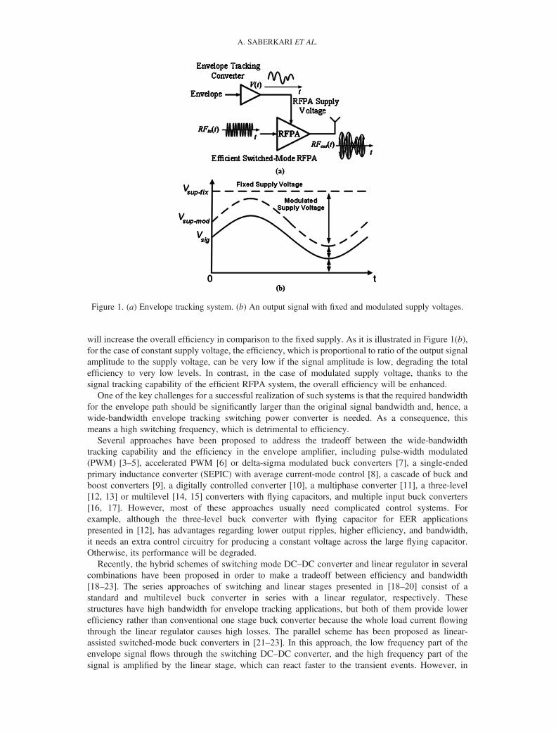
Figure 1. (a) Envelope tracking system. (b) An output signal with fixed and modulated supply voltages.
A. SABERKARI ET AL.
will increase the overall efficiency in comparison to the fixed supply. As it is illustrated in Figure 1(b),for the case of constant supply voltage, the efficiency, which is proportional to ratio of the output signalamplitude to the supply voltage, can be very low if the signal amplitude is low, degrading the totalefficiency to very low levels. In contrast, in the case of modulated supply voltage, thanks to thesignal tracking capability of the efficient RFPA system, the overall efficiency will be enhanced.
One of the key challenges for a successful realization of such systems is that the required bandwidthfor the envelope path should be significantly larger than the original signal bandwidth and, hence, awide-bandwidth envelope tracking switching power converter is needed. As a consequence, thismeans a high switching frequency, which is detrimental to efficiency.
Several approaches have been proposed to address the tradeoff between the wide-bandwidthtracking capability and the efficiency in the envelope amplifier, including pulse-width modulated(PWM) [3–5], accelerated PWM [6] or delta-sigma modulated buck converters [7], a single-endedprimary inductance converter (SEPIC) with average current-mode control [8], a cascade of buck andboost converters [9], a digitally controlled converter [10], a multiphase converter [11], a three-level[12, 13] or multilevel [14, 15] converters with flying capacitors, and multiple input buck converters[16, 17]. However, most of these approaches usually need complicated control systems. Forexample, although the three-level buck converter with flying capacitor for EER applicationspresented in [12], has advantages regarding lower output ripples, higher efficiency, and bandwidth,it needs an extra control circuitry for producing a constant voltage across the large flying capacitor.Otherwise, its performance will be degraded.
Recently, the hybrid schemes of switching mode DC–DC converter and linear regulator in severalcombinations have been proposed in order to make a tradeoff between efficiency and bandwidth[18–23]. The series approaches of switching and linear stages presented in [18–20] consist of astandard and multilevel buck converter in series with a linear regulator, respectively. Thesestructures have high bandwidth for envelope tracking applications, but both of them provide lowerefficiency rather than conventional one stage buck converter because the whole load current flowingthrough the linear regulator causes high losses. The parallel scheme has been proposed as linear-assisted switched-mode buck converters in [21–23]. In this approach, the low frequency part of theenvelope signal flows through the switching DC–DC converter, and the high frequency part of thesignal is amplified by the linear stage, which can react faster to the transient events. However, in
DF BUCK CONVERTER FOR EER APPLICATIONS IN POWER SUPPLY OF RFPAS
order to achieve a proper efficiency, one of the difficulties of this approach is the output combinerblock which causes a voltage drop between the input and output signals, resulting high power losses[22]. Furthermore, the band separation technique presented in [23] depends on the employedmodulation and needs a complicated control system which results in more power losses anddegraded efficiency.
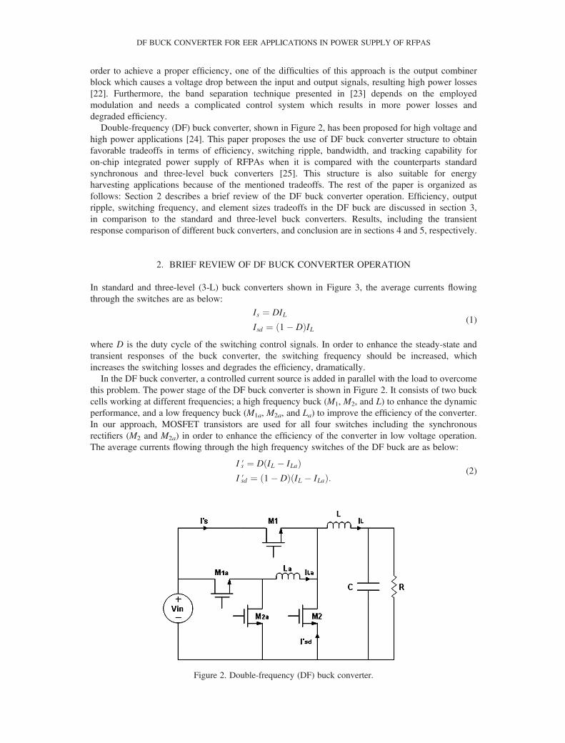
Double-frequency (DF) buck converter, shown in Figure 2, has been proposed for high voltage andhigh power applications [24]. This paper proposes the use of DF buck converter structure to obtainfavorable tradeoffs in terms of efficiency, switching ripple, bandwidth, and tracking capability foron-chip integrated power supply of RFPAs when it is compared with the counterparts standardsynchronous and three-level buck converters [25]. This structure is also suitable for energyharvesting applications because of the mentioned tradeoffs. The rest of the paper is organized asfollows: Section 2 describes a brief review of the DF buck converter operation. Efficiency, outputripple, switching frequency, and element sizes tradeoffs in the DF buck are discussed in section 3,in comparison to the standard and three-level buck converters. Results, including the transientresponse comparison of different buck converters, and conclusion are in sections 4 and 5, respectively.
2. BRIEF REVIEW OF DF BUCK CONVERTER OPERATION
In standard and three-level (3-L) buck converters shown in Figure 3, the average currents flowingthrough the switches are as below:
Is ¼ DIL
Isd ¼ 1� Dð ÞIL(1)
where D is the duty cycle of the switching control signals. In order to enhance the steady-state andtransient responses of the buck converter, the switching frequency should be increased, whichincreases the switching losses and degrades the efficiency, dramatically.
In the DF buck converter, a controlled current source is added in parallel with the load to overcomethis problem. The power stage of the DF buck converter is shown in Figure 2. It consists of two buckcells working at different frequencies; a high frequency buck (M1, M2, and L) to enhance the dynamicperformance, and a low frequency buck (M1a, M2a, and La) to improve the efficiency of the converter.In our approach, MOSFET transistors are used for all four switches including the synchronousrectifiers (M2 and M2a) in order to enhance the efficiency of the converter in low voltage operation.The average currents flowing through the high frequency switches of the DF buck are as below:
I ′s ¼ D IL � ILað ÞI ′sd ¼ 1� Dð Þ IL � ILað Þ: (2)
Figure 2. Double-frequency (DF) buck converter.
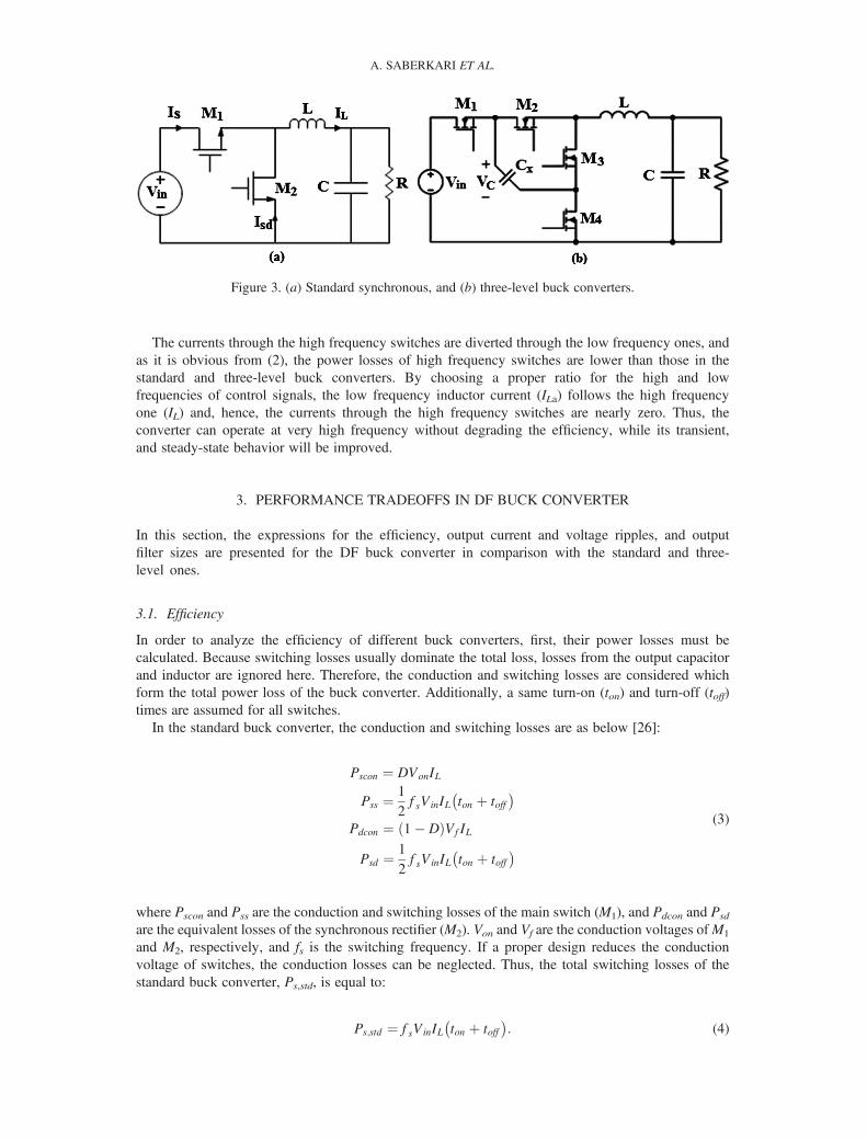
Figure 3. (a) Standard synchronous, and (b) three-level buck converters.
A. SABERKARI ET AL.
The currents through the high frequency switches are diverted through the low frequency ones, andas it is obvious from (2), the power losses of high frequency switches are lower than those in thestandard and three-level buck converters. By choosing a proper ratio for the high and lowfrequencies of control signals, the low frequency inductor current (ILa) follows the high frequencyone (IL) and, hence, the currents through the high frequency switches are nearly zero. Thus, theconverter can operate at very high frequency without degrading the efficiency, while its transient,and steady-state behavior will be improved.
3. PERFORMANCE TRADEOFFS IN DF BUCK CONVERTER
In this section, the expressions for the efficiency, output current and voltage ripples, and outputfilter sizes are presented for the DF buck converter in comparison with the standard and three-level ones.
3.1. Efficiency
In order to analyze the efficiency of different buck converters, first, their power losses must becalculated. Because switching losses usually dominate the total loss, losses from the output capacitorand inductor are ignored here. Therefore, the conduction and switching losses are considered whichform the total power loss of the buck converter. Additionally, a same turn-on (ton) and turn-off (toff)times are assumed for all switches.
In the standard buck converter, the conduction and switching losses are as below [26]:
Pscon ¼ DVonIL
Pss ¼ 12f sVinIL ton þ toff
� �Pdcon ¼ 1� Dð ÞVf IL
Psd ¼ 12f sVinIL ton þ toff
� �(3)
where Pscon and Pss are the conduction and switching losses of the main switch (M1), and Pdcon and Psd
are the equivalent losses of the synchronous rectifier (M2). Von and Vf are the conduction voltages ofM1
and M2, respectively, and fs is the switching frequency. If a proper design reduces the conductionvoltage of switches, the conduction losses can be neglected. Thus, the total switching losses of thestandard buck converter, Ps,std, is equal to:
Ps;std ¼ f sVinIL ton þ toff� �
: (4)
DF BUCK CONVERTER FOR EER APPLICATIONS IN POWER SUPPLY OF RFPAS
In the DF buck converter, the average currents flowing through the high frequency and lowfrequency inductors are approximately 0.5ILa and (IL�0.5ILa), respectively [24]. Hence, on the onehand, the losses of the high frequency cell are as below:
Pscon;H ¼ 0:5DVonILa
Pss;H ¼ 14f HVinILa ton þ toff
� �Pdcon;H ¼ 0:5 1� Dð ÞVf ILa
Psd;H ¼ 14f HVinILa ton þ toff
� �(5)
where Pscon,H and Pss,H are the conduction and switching losses of the main switch (M1), and Pdcon,H
and Psd,H are the equivalent losses of the synchronous rectifier (M2). In the same way, the losses ofthe low frequency cell are:
Pscon;L ¼ DVon IL � 0:5ILað ÞPss;L ¼ 1
2f LVin IL � 0:5ILað Þ ton þ toff
� �Pdcon;L ¼ 1� Dð ÞVf IL � 0:5ILað ÞPsd;L ¼ 1
2f LVin IL � 0:5ILað Þ ton þ toff
� �(6)
where Pscon,L and Pss,L are the conduction and switching losses of the main switch (M1a), and Pdcon,L
and Psd,L are the equivalent losses of the synchronous rectifier (M2a). fH and fL are the switchingfrequencies of high and low frequency buck cells, respectively. The total conduction loss of the DFbuck, which equals sum of the conduction losses of the high and low frequency cells, isapproximately the same as the standard buck. Additionally, because ILa is small in comparison withthe inductor average current, the switching loss of the high frequency cell can be neglected and thetotal switching losses of the DF buck, Ps,DF, is equal to:
Ps;DF ¼ f LVinIL ton þ toff� �
: (7)
As it is obvious from (4) and (7), the efficiency of the DF buck is much better than the standard buckbecause of its lower frequency, which is because of the diverting the current to the low frequency cell.
On the other hand, the conduction and switching losses of the three-level buck converter are asbelow:
Pscon ¼ 2DVonIL
Pss ¼ 12f s Vin � VCð ÞIL ton þ toff
� � ¼ 14f sVinIL ton þ toff
� �Pdcon ¼ 2 1� Dð ÞVf IL
Psd ¼ 12f s Vin � VCð ÞIL ton þ toff
� � ¼ 14f sVinIL ton þ toff
� �(8)
where VC is the flying capacitor voltage which equals Vin/2. The total conduction losses of the three-level buck are twice the standard and DF buck converters. Additionally, the total switching losses ofthe three-level buck, Ps,3-L, is as below:
Ps;3�L ¼ 12f sVinIL ton þ toff
� �: (9)
At the same output ripple, if we neglect the effect of conduction losses, the switching loss of the DFbuck will be lower than that of the three-level one by choosing fL<1/2 fs. Therefore, the efficiency of
A. SABERKARI ET AL.
the DF buck depends on the low frequency buck cell. As a consequence, by lowering it, higherefficiency can be obtained rather than three-level buck.
3.2. Ripple comparison
The high frequency inductor current ripple and the output voltage ripple for the DF buck converter areas below:
ΔiDF ¼ Vin
2Lf H1� Dð ÞD
ΔvDF ¼ Vin
16LCf 2H1� Dð ÞD:
(10)
The maximum ripples occur at the duty cycle equal to 0.5, and their values are given by:
ΔiDF;Max ¼ Vin
8Lf H
ΔvDF;Max ¼ Vin
64LCf 2H:
(11)
The low frequency inductor current ripple of the DF buck is as follows:
Δia;DF ¼ Vin
4Laf LD: (12)
As it can be seen, the output voltage and high frequency inductor current ripples of the DF buckdepend on fH (the high frequency cell) while its efficiency depends on fL.
For the standard buck converter, the ripples can be derived like (10) and (11) by substituting fsinstead of fH. Because of the fact that, increasing the switching frequency of the high frequency celldoes not affect the efficiency of DF, so the DF buck can have fewer ripples in comparison to thestandard buck at the same efficiency.
On the other hand, for the three-level buck, the ripples are equal to [12]:
Δi3�L ¼ Vin
2Lf s0:5� Dð ÞD 0 < D < 0:5
Δi3�L ¼ Vin
2Lf s1� Dð Þ D� 0:5ð Þ 0:5 < D < 1
Δv3�L ¼ Vin
32LCf 2s0:5� Dð ÞD 0 < D < 0:5
Δv3�L ¼ Vin
32LCf 2s1� Dð Þ D� 0:5ð Þ 0:5 < D < 1:
(13)
The maximum ripples occur at duty cycles equal to 0.25 and 0.75 as below:
Δi3�L;Max ¼ Vin
32Lf s
Δv3�L;Max ¼ Vin
512LCf 2s:
(14)
DF BUCK CONVERTER FOR EER APPLICATIONS IN POWER SUPPLY OF RFPAS
In order to have a ripple comparison between different buck converters, the ripples of the DF buck in(11) are rewritten based on the frequency ratio of high and low frequency cells, M, (fH=M fL), asfollows:
ΔiDF;Max ¼ Vin
8Lf L
1M
ΔvDF;Max ¼ Vin
64LCf 2L
1M
� �2
:
(15)
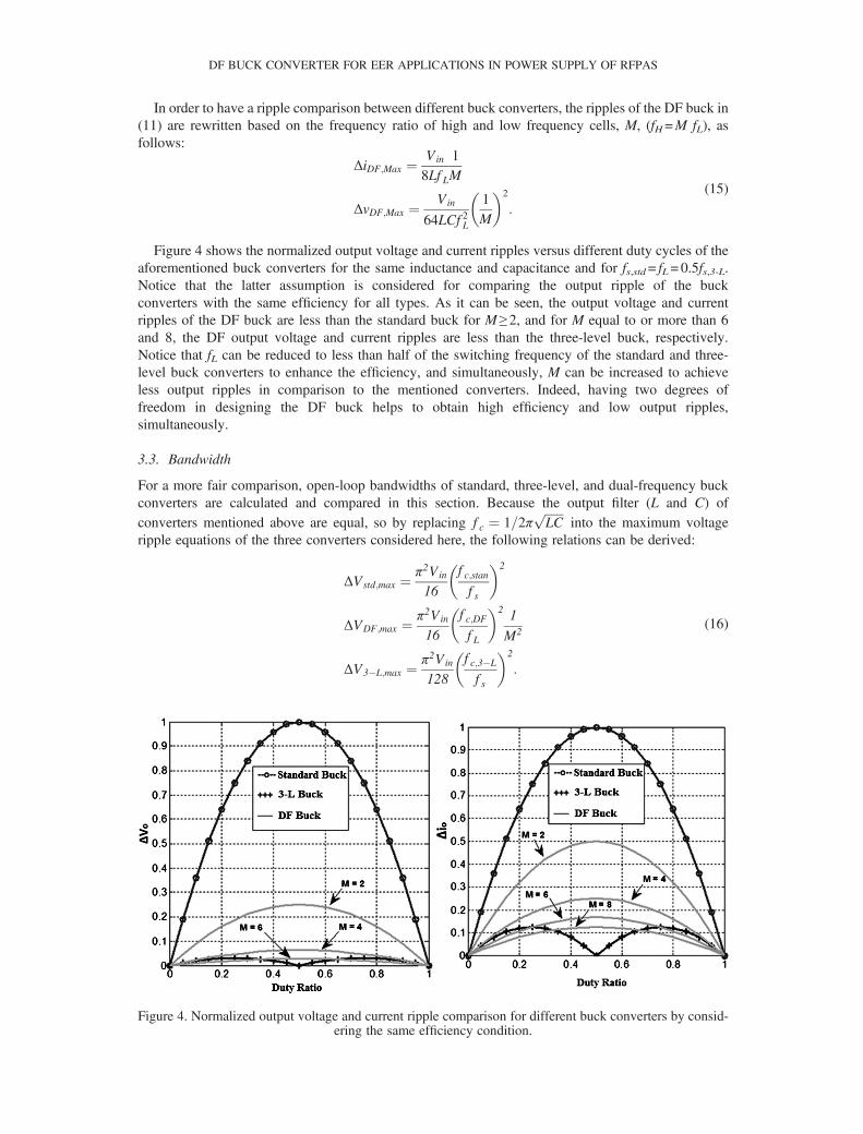
Figure 4 shows the normalized output voltage and current ripples versus different duty cycles of theaforementioned buck converters for the same inductance and capacitance and for fs,std= fL=0.5fs,3-L.Notice that the latter assumption is considered for comparing the output ripple of the buckconverters with the same efficiency for all types. As it can be seen, the output voltage and currentripples of the DF buck are less than the standard buck for M≥ 2, and for M equal to or more than 6and 8, the DF output voltage and current ripples are less than the three-level buck, respectively.Notice that fL can be reduced to less than half of the switching frequency of the standard and three-level buck converters to enhance the efficiency, and simultaneously, M can be increased to achieveless output ripples in comparison to the mentioned converters. Indeed, having two degrees offreedom in designing the DF buck helps to obtain high efficiency and low output ripples,simultaneously.
3.3. Bandwidth
For a more fair comparison, open-loop bandwidths of standard, three-level, and dual-frequency buckconverters are calculated and compared in this section. Because the output filter (L and C) ofconverters mentioned above are equal, so by replacing f c ¼ 1=2π
ffiffiffiffiffiffiLC
pinto the maximum voltage
ripple equations of the three converters considered here, the following relations can be derived:
ΔVstd;max ¼ π2Vin
16
f c;stanf s
� �2
ΔVDF;max ¼ π2Vin
16
f c;DFf L
� �2 1
M2
ΔV3�L;max ¼ π2Vin
128
f c;3�L
f s
� �2
:
(16)
Figure 4. Normalized output voltage and current ripple comparison for different buck converters by consid-ering the same efficiency condition.
A. SABERKARI ET AL.
By assuming the same efficiency (that is, fs,std= fL=0.5fs,3-L) and same voltage ripples, the open-loopbandwidth (fC) of these three converters can be obtained as below:
f c;3�L ¼ 4ffiffiffi2
pf c;std
f c;DF ¼ M
4ffiffiffi2
p f c;3�L
f c;DF ¼ M f c;std:
(17)
As a result, for M equal to or greater than 2 and 6, the open-loop bandwidth of DF buck ismore than that of standard and three-level buck converters, respectively. Moreover, because it is
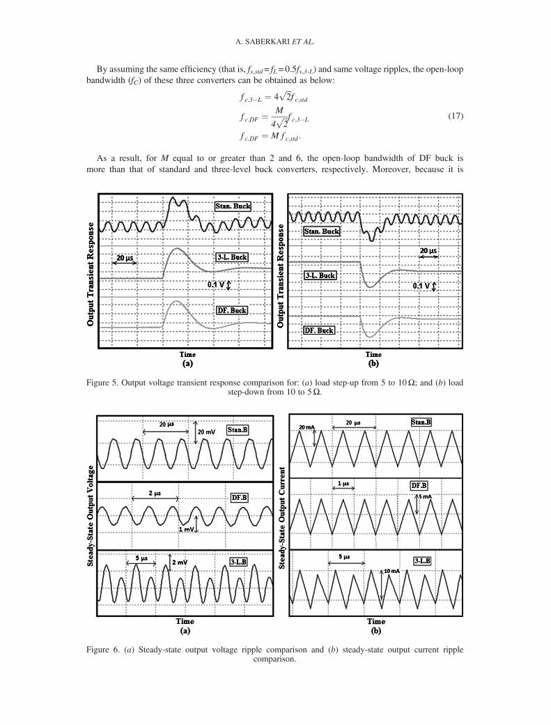
Figure 5. Output voltage transient response comparison for: (a) load step-up from 5 to 10Ω; and (b) loadstep-down from 10 to 5Ω.
Figure 6. (a) Steady-state output voltage ripple comparison and (b) steady-state output current ripplecomparison.
DF BUCK CONVERTER FOR EER APPLICATIONS IN POWER SUPPLY OF RFPAS
possible to increase the high frequency of the DF buck without degrading the efficiency, the filterelement sizes can be reduced significantly, and hence the open-loop bandwidth of the DF can beincreased.
Figure 7. Power supply ripple for different types of buck converters.
Figure 8. Efficiency comparison of the three buck converters.
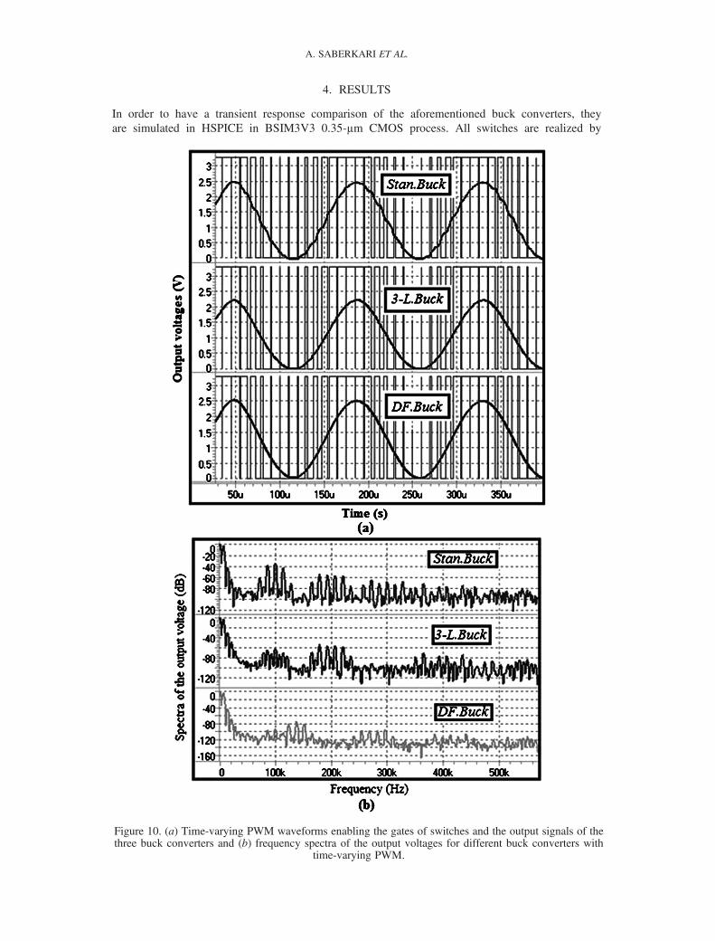
Figure 9. Test bench of the DF buck converter for evaluating the input signal tracking capability.
A. SABERKARI ET AL.
4. RESULTS
In order to have a transient response comparison of the aforementioned buck converters, theyare simulated in HSPICE in BSIM3V3 0.35-μm CMOS process. All switches are realized by
igure 10. (a) Time-varying PWM waveforms enabling the gates of switches and the output signals of theree buck converters and (b) frequency spectra of the output voltages for different buck converters with
Fth
time-varying PWM.
DF BUCK CONVERTER FOR EER APPLICATIONS IN POWER SUPPLY OF RFPAS
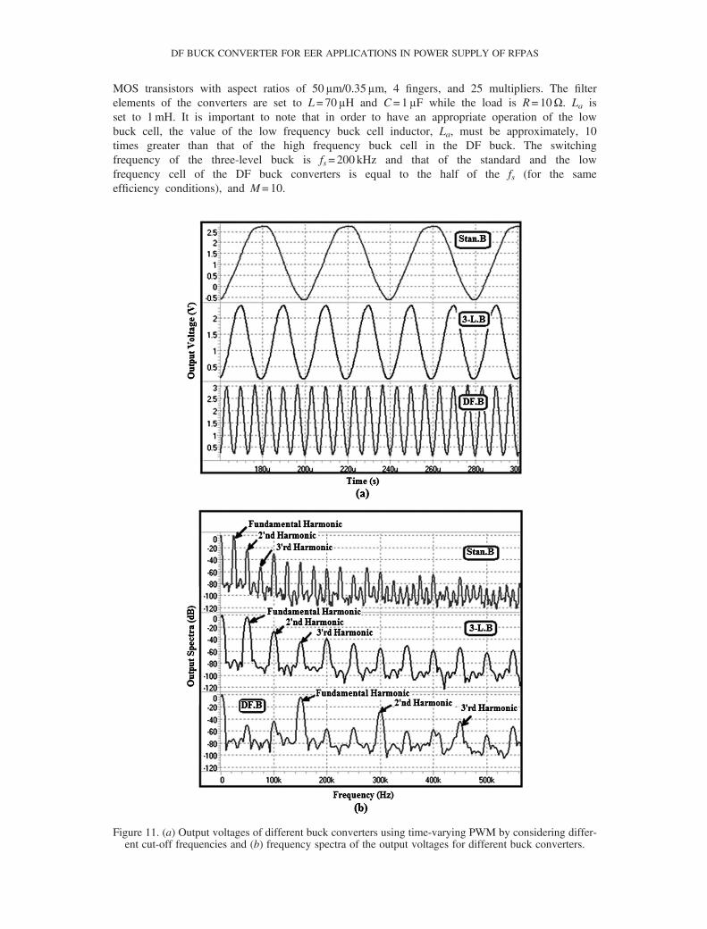
MOS transistors with aspect ratios of 50μm/0.35μm, 4 fingers, and 25 multipliers. The filterelements of the converters are set to L=70μH and C=1μF while the load is R=10Ω. La isset to 1mH. It is important to note that in order to have an appropriate operation of the lowbuck cell, the value of the low frequency buck cell inductor, La, must be approximately, 10times greater than that of the high frequency buck cell in the DF buck. The switchingfrequency of the three-level buck is fs=200 kHz and that of the standard and the lowfrequency cell of the DF buck converters is equal to the half of the fs (for the sameefficiency conditions), and M=10.
Figure 11. (a) Output voltages of different buck converters using time-varying PWM by considering differ-ent cut-off frequencies and (b) frequency spectra of the output voltages for different buck converters.
A. SABERKARI ET AL.
The output voltage transient responses of the converters for load step-up and down are shown inFigure 5. As it is obvious, the DF buck has the best transient response with lower overshoot andundershoot. The transient ripples for standard, three-level, and DF buck converters are 390, 310, and260mV, respectively. The steady-state output voltage and current ripples of the converters are shownin Figure 6. The voltage ripples of the DF, three-level, and standard buck converters are 1, 4, and25mV, respectively. Also the output current ripples are 8, 12, and 42mA, respectively for theaforementioned converters. Therefore, for the same efficiency conditions, the DF buck has loweroutput ripple rather than others meaning that the DF buck has the best performance from this pointof view.
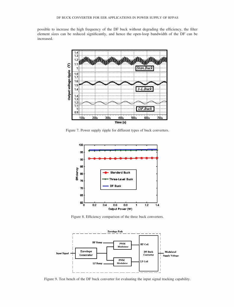
The ripple rejection ratio of the regulators, which is measured as power supply ripple (PSR), is thecriterion of rejecting the input voltage ripple at the output. Generally, this parameter shows the gainfrom the supply voltage (Vin in Figures 2 and 3) to the output as follows:
PSR ¼ 20 logoutput ripple
input ripple
� �: (18)
Obviously, the lower PSR is desirable. In order to measure this parameter for the aforementionedconverters by considering the same efficiency and filter element sizes, a sinusoidal voltage withamplitude of 200mV and frequency of fm=10KHz is added to the 2.5-VDC input voltage, andFigure 7 shows the output ripples for different buck converters. It is obvious that the DF buckconverter has the best response with 80-mV output ripple corresponding to �7.96dB ripplerejection. The output ripple for three-level and standard buck converters is 90 and 180mV,respectively, which is equivalent to a ripple rejection of �6.94 and �0.91 dB.
The efficiency comparison of the converters for different output power levels by considering thesame output voltage ripples and filter element sizes for all converters (fs,std=100kHz, fL,DF=10kHz,and fs,3-L=36kHz) and M=10 for DF buck is illustrated in Figure 8.
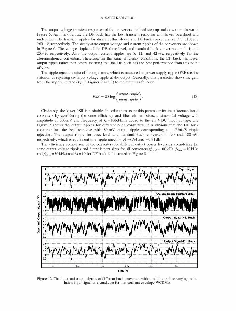
Figure 12. The input and output signals of different buck converters with a multi-tone time-varying modu-lation input signal as a candidate for non-constant envelope WCDMA.
DF BUCK CONVERTER FOR EER APPLICATIONS IN POWER SUPPLY OF RFPAS
As it is obvious, the efficiency of the DF buck is higher than that of the standard one because of itslower frequency of the low frequency buck cell. Additionally, the DF efficiency is a bit higher than thatof the three-level buck which is because of its lower conduction losses and a bit lower switchingfrequency of the low frequency cell. Therefore, for the same output voltage ripples and filterelements, the efficiency of the DF buck is higher than that of others leading to a perfect performanceof the DF buck converter.
In the case that fL,DF is set to the half of fs,3-L, the switching losses of both converters are the same,and the little difference is because of the amount of their conduction losses. Hence, we expect anapproximately equal efficiency for both of them.
For EER applications, the basis of buck converter operation is as envelope tracking amplifier.Therefore, it is interested to compare the performance of different buck converters under time-varying modulation signals by applying time-varying PWM. The test bench of the DF buckconverter used for evaluating the single and multi-frequency sinusoidal signal tracking capabilityis shown in Figure 9. First, a sinusoidal waveform with fm=7kHz is applied as a modulationsignal and the same efficiency condition, and filter element sizes are considered for all types ofconverters. Figure 10(a) illustrates the PWM signals and output voltages of different buckconverters. As it is expected, in all cases, the output voltages vary from 0 to Vin and can trackthe modulation signal, but with different ripples. In order to have a better ripple comparison,
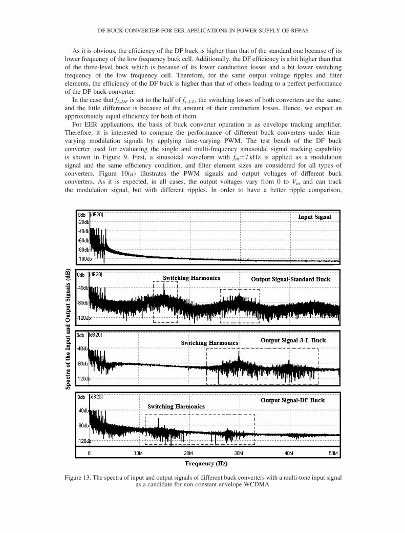
Figure 13. The spectra of input and output signals of different buck converters with a multi-tone input signalas a candidate for non-constant envelope WCDMA.
A. SABERKARI ET AL.
Figure 10(b) shows the frequency spectra of output voltages for different buck converters withmodulated PWM, and as it can be seen, the switching harmonics of the DF buck aresignificantly smaller, which is 16 dB lower than the three level and 40 dB lower than the standardbuck converter.
On the other hand, the DF buck is capable to support and track time-varying modulation sinusoidalwaveforms with higher frequencies (fm) rather than the two other buck converters. This aspectindicates a higher slew-rate for the DF buck. In fact, the low frequency buck cell of the DF buckconverter tracks the low frequency part of the envelope (time-varying modulation) signal and thehigh frequency buck cell tracks the high frequency counterpart. In order to provide a comparison,sinusoidal signals with fm equals to the bandwidth or cut-off frequency of each converter (fC) areapplied to produce the corresponding PWM signals. Switching frequencies are chosen so that thesame efficiency condition is obtained for all types of the buck converters (fs,std=100 kHz,fL,DF=100kHz, fs,3-L=200kHz, and M=10 for DF buck). The cut-off frequencies are chosen to havea same level of fundamental signal, second, and third harmonics at the spectrum of the outputvoltages (for more fair comparison). Thus, the higher the cut-off frequency is, the higher the slew-rate is, for the same amplitude of output signals. The frequency spectra and the time domain ofoutput voltages for the different buck converters are illustrated in Figure 11, by choosing fC, andhence fm, equals 25 kHz, 50 kHz, and 150 kHz for the standard, three-level, and DF buck converters,respectively. As it is obvious, the fundamental, second, and third harmonics of the output voltagesare the same. Furthermore, the DF buck can track a sinusoidal signal with higher frequency ratherthan the other converters.
In order to evaluate the non-constant envelope tracking capability of the aforementionedconverters, two comparisons are performed. For this purpose, two multi-tone signals, one of themwith 64 logarithmic distributed frequency components in the range of 100Hz to 3.2MHz (as acandidate for WCDMA) and another one with 77 logarithmic distributed frequency components inthe range of 100Hz to 20MHz (as a candidate for LTE), are applied as time-varying modulation
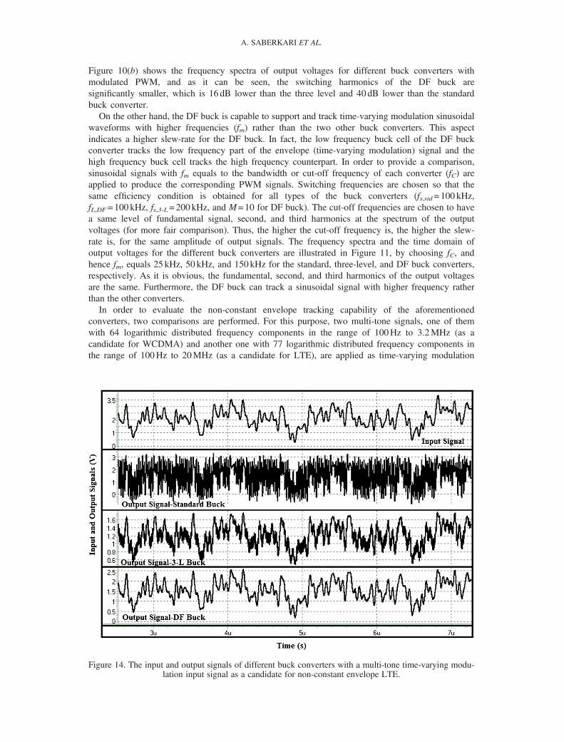
Figure 14. The input and output signals of different buck converters with a multi-tone time-varying modu-lation input signal as a candidate for non-constant envelope LTE.
DF BUCK CONVERTER FOR EER APPLICATIONS IN POWER SUPPLY OF RFPAS
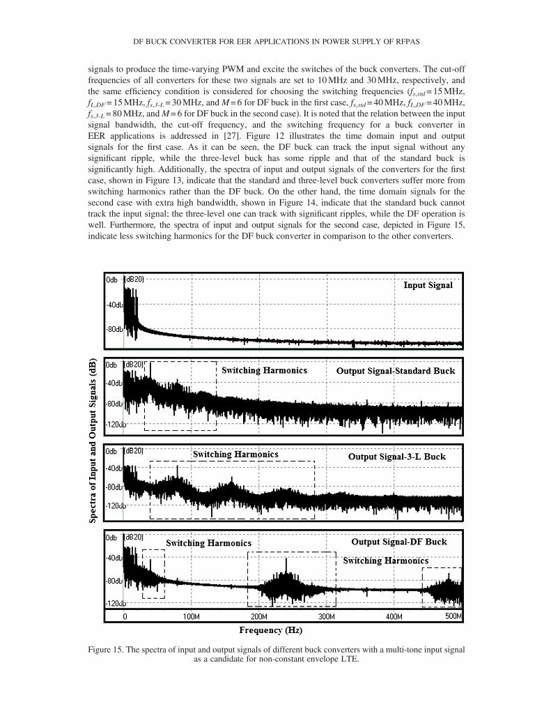
signals to produce the time-varying PWM and excite the switches of the buck converters. The cut-offfrequencies of all converters for these two signals are set to 10MHz and 30MHz, respectively, andthe same efficiency condition is considered for choosing the switching frequencies (fs,std=15MHz,fL,DF=15MHz, fs,3-L=30MHz, andM=6 for DF buck in the first case, fs,std=40MHz, fL,DF=40MHz,fs,3-L=80MHz, andM=6 for DF buck in the second case). It is noted that the relation between the inputsignal bandwidth, the cut-off frequency, and the switching frequency for a buck converter inEER applications is addressed in [27]. Figure 12 illustrates the time domain input and outputsignals for the first case. As it can be seen, the DF buck can track the input signal without anysignificant ripple, while the three-level buck has some ripple and that of the standard buck issignificantly high. Additionally, the spectra of input and output signals of the converters for the firstcase, shown in Figure 13, indicate that the standard and three-level buck converters suffer more fromswitching harmonics rather than the DF buck. On the other hand, the time domain signals for thesecond case with extra high bandwidth, shown in Figure 14, indicate that the standard buck cannottrack the input signal; the three-level one can track with significant ripples, while the DF operation iswell. Furthermore, the spectra of input and output signals for the second case, depicted in Figure 15,indicate less switching harmonics for the DF buck converter in comparison to the other converters.
Figure 15. The spectra of input and output signals of different buck converters with a multi-tone input signalas a candidate for non-constant envelope LTE.
A. SABERKARI ET AL.
5. CONCLUSION
Using the DF buck converter structure as a candidate topology for integrated power supply of RFPAsand EER applications is proposed in this paper. Diverting the high frequency current to the lowfrequency cell in the DF buck, will result in obtaining favorable tradeoffs in terms of efficiency,switching ripple, bandwidth, and envelope tracking capability. It is shown that having two degreesof freedom in designing the DF buck helps to obtain high efficiency and low output ripples,simultaneously. Performance analysis is done with regards to the mentioned indexes, and the results,validated in HSPICE in BSIM3V3 0.35-μm CMOS process, reveal the advantages of theaforementioned buck in comparison to the standard and three-level buck converters.
REFERENCES
1. Stauth J, Sanders S. Dynamic power supply design for high efficiency wireless transmitters. Department of ElectricalEngineering and Computer Sciences, University of California, Berkeley, CA, Tech.Rep. UCB/EECS-2006-72, 2006.
2. Raab FH, Asbeck P, Cripps S, Kenington PB, Popovic ZB, Pothecary N, Sevic JF, Sokal NO. Power amplifiers andtransmitters for RF and microwave. IEEE Transactions on Microwave Theory and Techniques 2002; 50(3):814–826.
3. Midya P, Haddad K, Connell L, Bergstedt S, Roeckner B. Tracking power converter for supply modulation of RFpower amplifiers. Proceedings IEEE Power Electronics Specialists Conference (PESC’01) 2001; 1:1540–1545.
4. Staudinger J, Gilsdorf B, Newman D, Norris G, Sadowniczak G, Sherman R, Quach T. High efficiency CDMA RFpower amplifier using dynamic envelope tracking technique. Proceedings IEEE MTT-S International MicrowaveSymposium Digest 2000; 2:873–876.
5. Abedinpour S, Deligoz K, Desai J, Figiel M, Kiaei S. Monolithic supply modulated RF power amplifier and DC–DCpower converter IC. Proceedings IEEE MTT-S International Microwave Symposium Digest. 2003; 1:A89–A92.
6. Chen JJ, Hwang BH, Jhang YC, Hwang YS, Yu CC. A new fast-response buck converter using accelerated pulse-width-modulation techniques. International Journal of Circuit Theory and Applications 2013; 41(8):854–865.
7. Tormo AG, Poveda A, Alarcon E, Guinjoan F. Design-oriented characterisation of adaptive asynchronous ΣΔ mod-ulation switching power amplifiers for bandlimited signals. Proceedings IEEE International Symposium on Circuitsand Systems (ISCAS’09) 2009:2882–2885.
8. Anderson DR, Cantrell WH. High-efficiency high-level modulator for use in dynamic envelope tracking CDMA RFpower amplifiers. Proceedings IEEE MTT-S International Microwave Symposium Digest 2001; 3:1509–1512.
9. Midya P, Haddad K, Miller M. Buck or boost tracking power converter. IEEE Power Electronics Letters 2004;2(4):131–134.
10. Yousefzadeh V, Wang N, Popovic Z, Maksimovic D. A digitally controlled DC/DC converter for an RF power am-plifier. IEEE Transactions on Power Electronics 2006; 21(1):164–172.
11. Qiu Y, Xu M, Yao K, Sun J, Lee FC. Multifrequency small-signal model for buck and multiphase buck converters.IEEE Transactions on Power Electronics 2006; 21(5):1185–1192.
12. Yousefzadeh V, Alarcon E, Maksimovic D. Three-level buck converter for envelope tracking in RF power amplifiers.Proc. IEEE Applied Power Electronics Conference (APEC’05) 2005; 3:1588–1594.
13. Rodrigues JP, Mussa SA, Heldwein ML, Perin AJ. Three-level ZVS active clamping PWM for the DC–DC buckconverter. IEEE Transactions on Power Electronics 2009; 24(10):2249–2258.
14. Meynard TA, Foch H. Multi-level conversion: high voltage choppers and voltage-source inverters. ProceedingsIEEE Power Electronics Specialists Conference (PESC’92) 1992; 1:397–403.
15. Meynard TA, Foch H, Thomas P, Courault I, Jakob R, Nahrstaedt M. Multicell converters: basic concepts and indus-try applications. IEEE Transactions on Industrial Electronics 2002; 49(5):955–964.
16. Rodrıguez M, Miaja PF, Rodrıguez A, Sebastian J. A multiple-input digitally controlled buck converter for envelopetracking applications in radiofrequency power amplifiers. IEEE Transactions on Power Electronics 2010;25(2):369–381.
17. Huang H, Bao J, Zhang L. A MASH-controlled multilevel power converter for high-efficiency RF transmitters. IEEETransactions on Power Electronics 2011; 26(4):1205–1214.
18. Gjanci J, Chowdhury MH. A hybrid scheme for on-chip voltage regulation in system-on-a-chip (SOC). IEEE Trans-actions on VLSI System 2011; 19(11):1949–1959.
19. Vasic M, Garcıa O, Oliver JA, Alou P, Dıaz D, Cobos JA. Multilevel power supply for high-efficiency RF amplifiers.IEEE Transactions on Power Electronics 2010; 25(4):1078–1089.
20. Modi S, Balsara P, Eliezer O. Envelope tracking using transient waveform switching shaping supply modulation. In-ternational Journal of Circuit Theory and Applications 2013. doi:10.1002/cta.
21. Kim I, Woo YY, Moon J, Kim J, Kim B. High-efficiency hybrid EER transmitter using optimized power amplifier.IEEE Transactions on Microwave Theory and Techniques 2008; 56(11):2582–2593.
22. Miaja PF, Rodrıguez M, Rodrıguez A, Sebastian J. A linear assisted DC/DC converter for envelope tracking and en-velope elimination and restoration applications. IEEE Transactions on Power Electronics 2012; 27(7):3302–3309.
23. Yousefzadeh V, Alarcon E, Maksimovic D. Band separation and efficiency optimization in linear-assisted switchingpower amplifiers. Proceedings IEEE Power Electronics Specialists Conference, (PESC’06) 2006:1–7.

DF BUCK CONVERTER FOR EER APPLICATIONS IN POWER SUPPLY OF RFPAS
24. Du X, Zhou L, Tai HM. Double-frequency buck converter. IEEE Transactions on Industrial Electronics 2009;56(5):1690–1698.
25. Shirmohammadli V, Saberkari A, Alarcon E. Performance analysis of dual-frequency buck converter for integratedpower management. Proceedings IEEE. Power Electronics and Drive Systems and Technologies Conference(PEDSTC’14) 2014:402–407.
26. Mohan N, Undeland TM, Robbins WP. Power Electronics: Converters, Applications, and Design (3rd edn). Wiley:New York, 2003.
27. Marco L, Alarcon E, Maksimovic D. Effects of switching power converter nonidealities in envelope elimination andrestoration technique. Proceedings IEEE International Symposium on Circuits and Systems (ISCAS’06)2006:3137–3140.
Related Documents