DIO4802 Users Manual fi Real Time Devices, Inc. Accessing the Analog World ® Publication No. 4802-9526

Welcome message from author
This document is posted to help you gain knowledge. Please leave a comment to let me know what you think about it! Share it to your friends and learn new things together.
Transcript
DIO4802User�s Manual
®
Real Time Devices, Inc.�Accessing the Analog World�
®
Publication No. 4802-9526

DIO4802User�s Manual
®
REAL TIME DEVICES, INC.Post Office Box 906
State College, Pennsylvania 16804 USAPhone: (814) 234-8087
FAX: (814) 234-5218

Published byReal Time Devices, Inc.
P.O. Box 906State College, PA 16804 USA
Copyright © 1995 by Real Time Devices, Inc.All rights reserved
Printed in U.S.A.
9526
Table of Contents
i
INTRODUCTION .................................................................................................................................... i-1
Digital I/O ............................................................................................................................................................... i-38254 Timer/Counter ................................................................................................................................................ i-3What Comes With Your Board ............................................................................................................................... i-3Board Accessories ................................................................................................................................................... i-3
Hardware Accessories ......................................................................................................................................... i-3Using This Manual .................................................................................................................................................. i-4When You Need Help ............................................................................................................................................. i-4
CHAPTER 1 � BOARD SETTINGS .................................................................................................. 1-1
Factory-Configured Switch and Jumper Settings .................................................................................................. 1-3P7 � 8254 Clock and Gate Source Select (Factory Settings: See Figure 1-2) ................................................ 1-5S1 � Base Address (Factory Setting: 300 hex (768 decimal)) ......................................................................... 1-6S2 through S5 � Buffer Bypass Switches (Factory Setting: OPEN (Not Bypassed)) ..................................... 1-7
Pull-up/Pull-down Resistors on Digital I/O Lines ................................................................................................. 1-9
CHAPTER 2 � BOARD INSTALLATION ....................................................................................... 2-1
Board Installation ................................................................................................................................................... 2-3External I/O Connections ....................................................................................................................................... 2-3
Connecting the Digital I/O ................................................................................................................................. 2-4Connecting the Timer/Counter I/O .................................................................................................................... 2-4Connecting the External Interrupt ...................................................................................................................... 2-4
Running the 4802DIAG Diagnostics Program ...................................................................................................... 2-4
CHAPTER 3 � HARDWARE DESCRIPTION................................................................................. 3-1
Digital I/O, Programmable Peripheral Interface .................................................................................................... 3-3Timer/Counters ...................................................................................................................................................... 3-4
CHAPTER 4 � I/O MAPPING ............................................................................................................ 4-1
Defining the I/O Map ............................................................................................................................................. 4-3BA + 0: PPI0 Port A � Digital I/O (Read/Write) ............................................................................................ 4-4BA + 1: PPI0 Port B � Digital I/O (Read/Write) ............................................................................................ 4-4BA + 2: PPI0 Port C � Digital I/O (Read/Write) ............................................................................................. 4-4BA + 3: 8255 PPI0 Control Word (Write Only) ............................................................................................... 4-4BA + 4: PPI1 Port A � Digital I/O (Read/Write) ............................................................................................ 4-6BA + 5: PPI1 Port B � Digital I/O (Read/Write) ............................................................................................ 4-6BA + 6: PPI1 Port C � Digital I/O (Read/Write) ............................................................................................. 4-6BA + 7: 8255 PPI1 Control Word (Write Only) ............................................................................................... 4-6BA + 8: 8254 Timer/Counter 0 (Read/Write) ................................................................................................... 4-8BA + 9: 8254 Timer/Counter 1 (Read/Write) ................................................................................................... 4-8BA + 10: 8254 Timer/Counter 2 (Read/Write) ................................................................................................. 4-8BA + 11: 8254 Timer/Counter Control Word (Write Only) ............................................................................. 4-8BA + 12: IRQ Status/IRQ Enable and Channel/Source Select (Read/Write) ................................................... 4-8BA + 13: Reset Board (Write Only) ................................................................................................................. 4-9BA + 14: Clear IRQ (Write Only) .................................................................................................................... 4-9BA + 15: Reserved ............................................................................................................................................ 4-9
Programming the DIO4802 .................................................................................................................................. 4-10Clearing and Setting Bits in a Port ....................................................................................................................... 4-10
ii
CHAPTER 5 � DIGITAL I/O ............................................................................................................. 5-1
Initializing the 8255 PPIs ....................................................................................................................................... 5-3Digital I/O Operations ............................................................................................................................................ 5-3Resetting the Digital Circuitry ............................................................................................................................... 5-3
CHAPTER 6 � TIMER/COUNTERS ................................................................................................. 6-1
CHAPTER 7 � INTERRUPTS ............................................................................................................ 7-1
Software Programmable Interrupts ........................................................................................................................ 7-3Basic Programming For Interrupt Handling .......................................................................................................... 7-3
What Is an Interrupt? ......................................................................................................................................... 7-3Interrupt Request Lines ...................................................................................................................................... 7-38259 Programmable Interrupt Controller .......................................................................................................... 7-3
Interrupt Mask Register (IMR) ...................................................................................................................... 7-3End-of-Interrupt (EOI) Command ................................................................................................................. 7-4
What Exactly Happens When an Interrupt Occurs? .......................................................................................... 7-4Using Interrupts in Your Programs .................................................................................................................... 7-4Writing an Interrupt Service Routine (ISR) ....................................................................................................... 7-4Saving the Startup Interrupt Mask Register (IMR) and Interrupt Vector .......................................................... 7-5Restoring the Startup IMR and Interrupt Vector ............................................................................................... 7-6Common Interrupt Mistakes .............................................................................................................................. 7-6
APPENDIX A � DIO4802 SPECIFICATIONS ................................................................................. A-1
APPENDIX B � CONNECTOR PIN ASSIGNMENTS .................................................................... B-1
APPENDIX C � COMPONENT DATA SHEETS ............................................................................ C-1
APPENDIX D � WARRANTY............................................................................................................ D-1
iii
List of Illustrations
1-1 Board Layout Showing Factory-Configured Settings .............................................................................. 1-41-2 8254 Clock and Gate Source Jumpers, P7 ................................................................................................ 1-51-3 8254 Circuit Diagram ............................................................................................................................... 1-51-4 Base Address Switch, S1 .......................................................................................................................... 1-61-5 Port C Buffer Circuitry ............................................................................................................................. 1-81-6 Port A Buffer Circuitry ............................................................................................................................. 1-81-7 Adding Pull-ups and Pull-downs to Some Digital I/O Lines ................................................................. 1-102-1 P2, P3, and P6 I/O Connector Pin Assignments ....................................................................................... 2-43-1 DIO4802 Block Diagram (PPI0) .............................................................................................................. 3-33-2 Timer/Counter Circuit Block Diagram ..................................................................................................... 3-46-1 8254 Timer/Counter Circuit Block Diagram ............................................................................................ 6-3

iv

i-1
INTRODUCTION

i-2

i-3
The DIO4802 is a general purpose digital I/O board for use in the IBM PC/XT/AT or compatible computer.Installed within a single full-size expansion slot in the computer, the DIO4802 features:
� 48 TTL/CMOS 8255-based programmable digital I/O lines,� Direct connection to opto-22 I/O system modules,� Buffered outputs for high driving capability,� Optional pull-up/pull-down resistors,� Simple I/O, strobed I/O, or bidirectional strobed I/O operation,� Three 16-bit timer/counters,� Software enabled interrupts (IRQ2-IRQ7),� QuickBASIC and C source code; diagnostics program.
The following paragraphs briefly describe the major functions of the board. A more detailed discussion of boardfunctions is included in Chapter 3, Hardware Operation, and Chapter 4, I/O Mapping. The board setup is describedin Chapter 1, Board Settings.
Digital I/O
The DIO4802 has 48 TTL/CMOS-compatible digital I/O lines which can be directly interfaced with externaldevices or signals to sense switch closures, trigger digital events, or activate solid-state relays. These lines areprovided by two 24-line on-board 8255 programmable peripheral interface chips, PPI0 and PPI1. Each 8255 can beoperated in one of the three modes supported by the 8255 chip: Mode 0, Mode 1, or Mode 2. To ensure high drivingcapacity, CMOS buffers are installed. TTL buffers are available on request. On-board switches bypass buffers forModes 1 and 2 support.
Pads for installing and activating pull-up or pull-down resistors are included on the board. Installation proce-dures are given at the end of Chapter 1, Board Settings.
8254 Timer/Counter
An 8254 programmable interval timer contains three 16-bit, 8 MHz timer/counters to support a wide range oftiming and counting functions. The clock, gate, and output pins for each of the timer/counters are available at P6, a20-pin on-board box header connector.
What Comes With Your Board
You receive the following items in your DIO4802 package:
� DIO4802 interface board� Software and diagnostics diskette with QuickBASIC and C source code� User�s manual
If any item is missing or damaged, please call Real Time Devices� Customer Service Department at(814) 234-8087. If you require service outside the U.S., contact your local distributor.
Board Accessories
In addition to the items included in your board package, Real Time Devices offers a full line of software andhardware accessories. Call your local distributor or our main office for more information about these accessories andfor help in choosing the best items to support your board�s application.
Hardware Accessories
Hardware accessories for the DIO4802 include the DOP series optoisolated digital input front-end boards, theDMR series mechanical relay output front-end boards, the TB50 terminal board and XB50 prototype/terminal boardfor easy signal access and prototype development, and XO50 ribbon cable assembly for interconnection to anopto-22 rack.

i-4
Using This Manual
This manual is intended to help you install your new board and get it running quickly, while also providingenough detail about the board and its functions so that you can enjoy maximum use of its features even in the mostcomplex applications. We assume that you already have an understanding of data acquisition principles and that youcan customize the example software or write your own applications programs.
When You Need Help
This manual and the example programs in the software package included with your board provide enoughinformation to properly use all of the board�s features. If you have any problems installing or using this board,contact our Technical Support Department, (814) 234-8087, during regular business hours, eastern standard time oreastern daylight time, or send a FAX requesting assistance to (814) 234-5218. When sending a FAX request, pleaseinclude your company�s name and address, your name, your telephone number, and a brief description of theproblem.
1-1
CHAPTER 1
BOARD SETTINGS
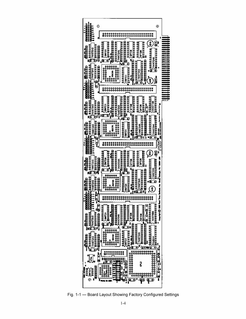
The DIO4802 has jumper and switch settings you can change ifnecessary for your application. The board is factory-configured aslisted in the table and shown on the layout diagram in the begin-ning of this chapter. Should you need to change these settings, usethese easy-to-follow instructions before you install the board inyour computer.
Two switches are provided for each of the two 8255 PPIs tobypass the Port A and/or Port C buffers for Modes 1 and 2 opera-tion.
Note that by installing resistor packs at the locations labeledaround each of the two 8255 PPIs and soldering jumpers as desiredon the associated pads, you can configure your 8255 digital I/Olines to be pulled up or pulled down. This procedure is explainednear the end of this chapter.

1-2

1-3
Factory-Configured Switch and Jumper Settings
Table 1-1 lists the factory settings of the user-configurable jumpers and switch on the DIO4802. Figure 1-1shows the board layout and the locations of the factory-set jumpers. The following paragraphs explain how tochange the factory settings. Pay special attention to the setting of S1, the base address switch, to avoid addresscontention when you first use your board in your system.
Table 1-1: Factory SettingsSwitch/Jumper Function Controlled
Factory Settings(Jumpers Installed)
P7Sets the clock and gate sources for the 8254timer/counter
CLK0: OSC; CLK1: OT0CLK2:OT1; GT2:EG2(timer/counters cascaded)
S1 Sets the base address 300 hex (768 decimal)
S2Bypasses 8255 #0Õs (PPI0) Port A buffers forMode 2 operation Open (buffers not bypassed)
S3Bypasses 8255 #0Õs (PPI0) Port C buffers forMode 1 or Mode 2 operation Open (buffers not bypassed)
S4Bypasses 8255 #1Õs (PPI1) Port A buffers forMode 2 operation Open (buffers not bypassed)
S5Bypasses 8255 #1Õs (PPI1) Port C buffers forMode 1 or Mode 2 operation Open (buffers not bypassed)
1-4
Fig. 1-1 � Board Layout Showing Factory Configured Settings
1-5
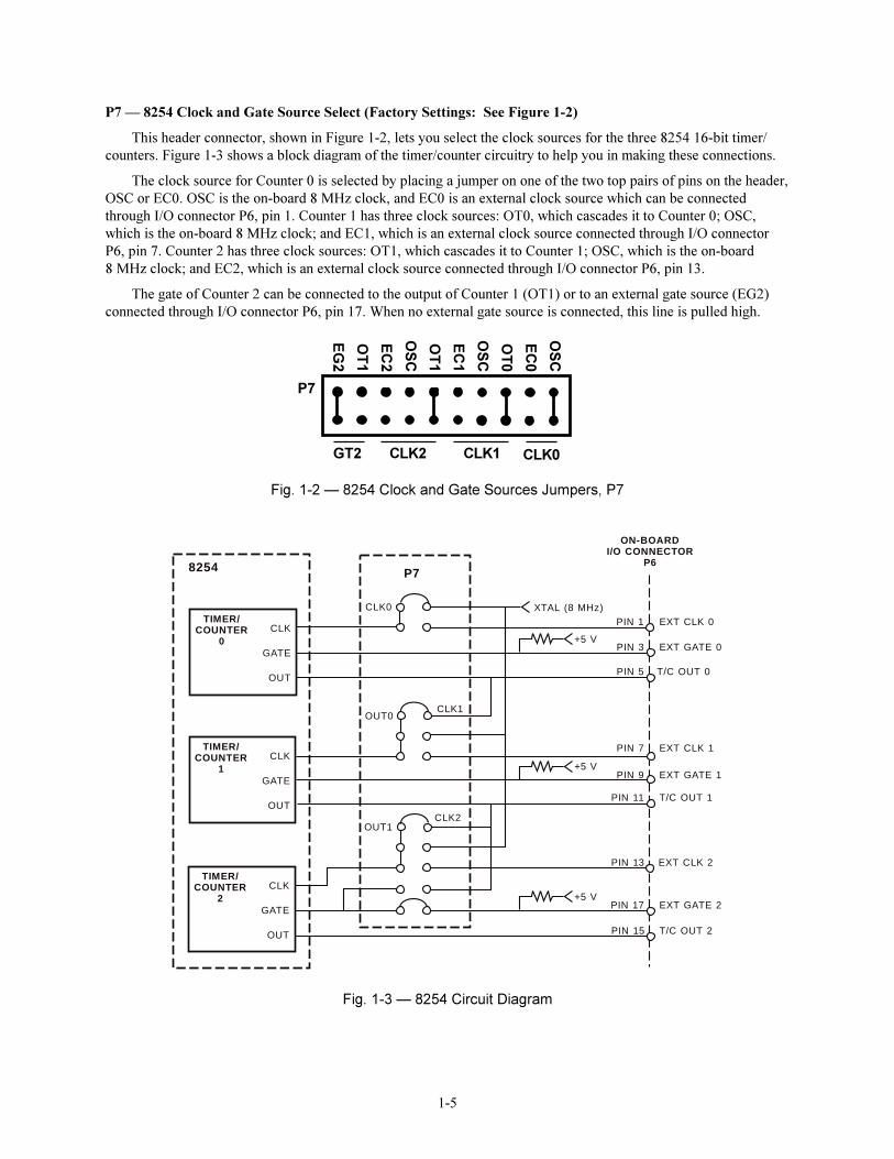
P7 � 8254 Clock and Gate Source Select (Factory Settings: See Figure 1-2)
This header connector, shown in Figure 1-2, lets you select the clock sources for the three 8254 16-bit timer/counters. Figure 1-3 shows a block diagram of the timer/counter circuitry to help you in making these connections.
The clock source for Counter 0 is selected by placing a jumper on one of the two top pairs of pins on the header,OSC or EC0. OSC is the on-board 8 MHz clock, and EC0 is an external clock source which can be connectedthrough I/O connector P6, pin 1. Counter 1 has three clock sources: OT0, which cascades it to Counter 0; OSC,which is the on-board 8 MHz clock; and EC1, which is an external clock source connected through I/O connectorP6, pin 7. Counter 2 has three clock sources: OT1, which cascades it to Counter 1; OSC, which is the on-board8 MHz clock; and EC2, which is an external clock source connected through I/O connector P6, pin 13.
The gate of Counter 2 can be connected to the output of Counter 1 (OT1) or to an external gate source (EG2)connected through I/O connector P6, pin 17. When no external gate source is connected, this line is pulled high.
OS
C
EC
0
OT
0
OS
C
EC
1
OT
1
OS
C
EC
2
OT
1
EG
2
CLK1
Fig. 1-2 � 8254 Clock and Gate Sources Jumpers, P7
P7
GT2 CLK2 CLK0
CLK1
CLK2
CLK0
ON-BOARDI/O CONNECTOR
P6
PIN 17
PIN 7
PIN 11
8254
TIMER/COUNTER
0CLK
GATE
OUT
TIMER/COUNTER
1CLK
GATE
OUT
TIMER/COUNTER
2CLK
GATE
OUT
PIN 1
PIN 15
XTAL (8 MHz)
P7
+5 V
+5 V
+5 V
PIN 3
PIN 5
PIN 9
PIN 13
T/C OUT 0
OUT0
OUT1
EXT CLK 0
T/C OUT 1
EXT CLK 1
EXT GATE 2
T/C OUT 2
EXT CLK 2
EXT GATE 0
EXT GATE 1
Fig. 1-3 � 8254 Circuit Diagram
1-6
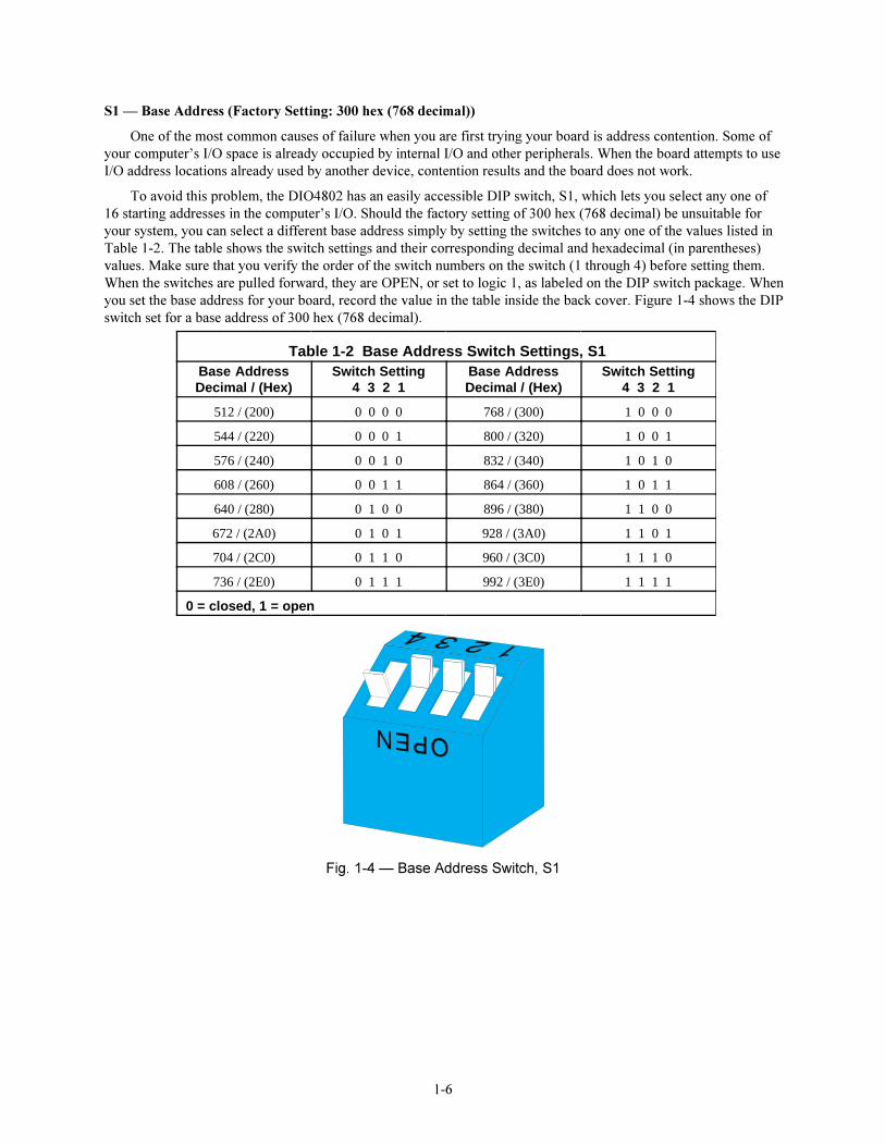
S1 � Base Address (Factory Setting: 300 hex (768 decimal))
One of the most common causes of failure when you are first trying your board is address contention. Some ofyour computer�s I/O space is already occupied by internal I/O and other peripherals. When the board attempts to useI/O address locations already used by another device, contention results and the board does not work.
To avoid this problem, the DIO4802 has an easily accessible DIP switch, S1, which lets you select any one of16 starting addresses in the computer�s I/O. Should the factory setting of 300 hex (768 decimal) be unsuitable foryour system, you can select a different base address simply by setting the switches to any one of the values listed inTable 1-2. The table shows the switch settings and their corresponding decimal and hexadecimal (in parentheses)values. Make sure that you verify the order of the switch numbers on the switch (1 through 4) before setting them.When the switches are pulled forward, they are OPEN, or set to logic 1, as labeled on the DIP switch package. Whenyou set the base address for your board, record the value in the table inside the back cover. Figure 1-4 shows the DIPswitch set for a base address of 300 hex (768 decimal).
Fig. 1-4 � Base Address Switch, S1
Table 1-2 Base Address Switch Settings, S1Base AddressDecimal / (Hex)
Switch Setting4 3 2 1
Base AddressDecimal / (Hex)
Switch Setting4 3 2 1
512 / (200) 0 0 0 0 768 / (300) 1 0 0 0
544 / (220) 0 0 0 1 800 / (320) 1 0 0 1
576 / (240) 0 0 1 0 832 / (340) 1 0 1 0
608 / (260) 0 0 1 1 864 / (360) 1 0 1 1
640 / (280) 0 1 0 0 896 / (380) 1 1 0 0
672 / (2A0) 0 1 0 1 928 / (3A0) 1 1 0 1
704 / (2C0) 0 1 1 0 960 / (3C0) 1 1 1 0
736 / (2E0) 0 1 1 1 992 / (3E0) 1 1 1 1
0 = closed, 1 = open
1-7
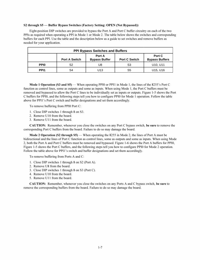
S2 through S5 � Buffer Bypass Switches (Factory Setting: OPEN (Not Bypassed))
Eight-position DIP switches are provided to bypass the Port A and Port C buffer circuitry on each of the twoPPIs as required when operating a PPI in Mode 1 or Mode 2. The table below shows the switches and correspondingbuffers for each PPI. Use the table and the description below as a guide to set switches and remove buffers asneeded for your application.
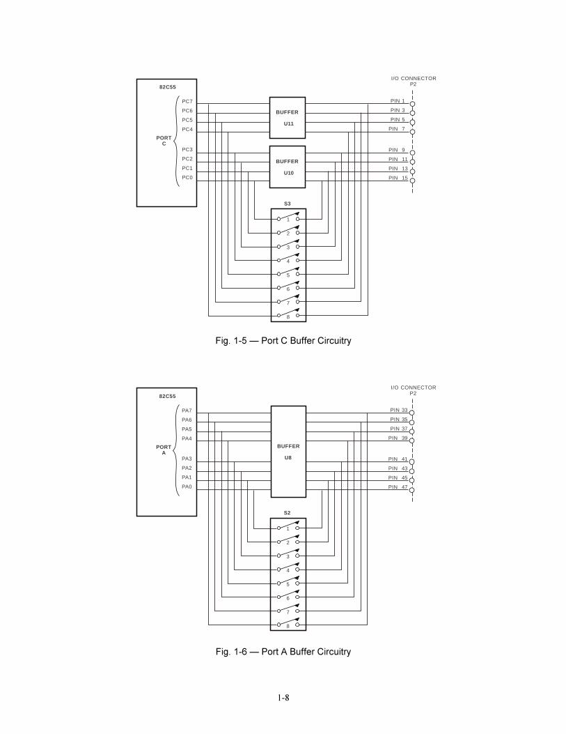
Mode 1 Operation (S3 and S5) � When operating PPI0 or PPI1 in Mode 1, the lines of the 8255�s Port Cfunction as control lines, some as outputs and some as inputs. When using Mode 1, the Port C buffers must beremoved and bypassed to allow the Port C lines to be individually set as inputs or outputs. Figure 1-5 shows the PortC buffers for PPI0, and the following steps tell you how to configure PPI0 for Mode 1 operation. Follow the tableabove for PPI1�s Port C switch and buffer designations and set them accordingly.
To remove buffering from PPI0 Port C:
1. Close DIP switches 1 through 8 on S3.2. Remove U10 from the board.3. Remove U11 from the board.
CAUTION: Remember, whenever you close the switches on any Port C bypass switch, be sure to remove thecorresponding Port C buffers from the board. Failure to do so may damage the board.
Mode 2 Operation (S2 through S5) � When operating the 8255 in Mode 2, the lines of Port A must bebidirectional and the lines of Port C function as control lines, some as outputs and some as inputs. When using Mode2, both the Port A and Port C buffers must be removed and bypassed. Figure 1-6 shows the Port A buffers for PPI0,Figure 1-5 shows the Port C buffers, and the following steps tell you how to configure PPI0 for Mode 2 operation.Follow the table above for PPI1�s switch and buffer designations and set them accordingly.
To remove buffering from Ports A and C:
1. Close DIP switches 1 through 8 on S2 (Port A).2. Remove U8 from the board.3. Close DIP switches 1 through 8 on S3 (Port C).4. Remove U10 from the board.5. Remove U11 from the board.
CAUTION: Remember, whenever you close the switches on any Ports A and C bypass switch, be sure toremove the corresponding buffers from the board. Failure to do so may damage the board.
PPI Bypass Switches and Buffers
Port A SwitchPort A
Bypass Buffer Port C SwitchPort C
Bypass Buffers
PPI0 S2 U8 S3 U10, U11
PPI1 S4 U13 S5 U15, U16
1-8
PIN 1
PIN 3
PIN 5
PIN 7
I/O CONNECTORP2
BUFFER
U11
BUFFER
U10
82C55
PORTC
S3
PIN 9
PIN 11
PIN 13
PIN 15
1
2
3
4
5
6
7
8
PC7
PC6
PC5
PC4
PC3
PC2
PC1
PC0
Fig. 1-5 � Port C Buffer Circuitry
PIN 33
PIN 35
PIN 37
PIN 39
I/O CONNECTORP282C55
PORTA
S2
PIN 41
PIN 43
PIN 45
PIN 47
1
2
3
4
5
6
7
8
PA7
PA6
PA5
PA4
PA3
PA2
PA1
PA0
BUFFER
U8
Fig. 1-6 � Port A Buffer Circuitry
1-9
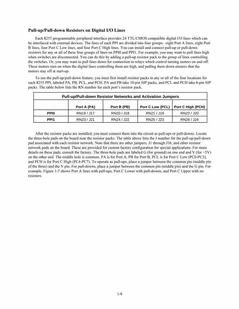
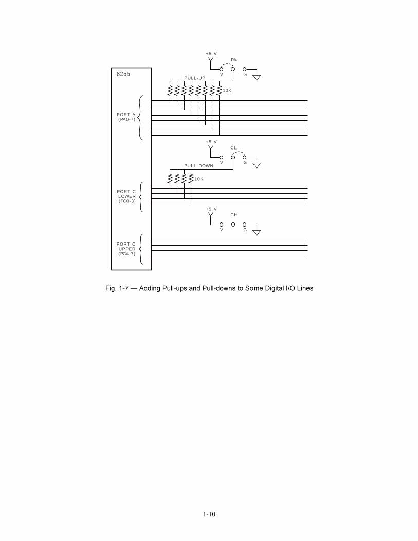
Pull-up/Pull-down Resistors on Digital I/O Lines
Each 8255 programmable peripheral interface provides 24 TTL/CMOS compatible digital I/O lines which canbe interfaced with external devices. The lines of each PPI are divided into four groups: eight Port A lines, eight PortB lines, four Port C Low lines, and four Port C High lines. You can install and connect pull-up or pull-downresistors for any or all of these four groups of lines on PPI0 and PPI1. For example, you may want to pull lines highwhen switches are disconnected. You can do this by adding a pull-up resistor pack to the group of lines controllingthe switches. Or, you may want to pull lines down for connection to relays which control turning motors on and off.These motors turn on when the digital lines controlling them are high, and pulling them down ensures that themotors stay off at start-up.
To use the pull-up/pull-down feature, you must first install resistor packs in any or all of the four locations foreach 8255 PPI, labeled PA, PB, PCL, and PCH. PA and PB take 10-pin SIP packs, and PCL and PCH take 6-pin SIPpacks. The table below lists the RN number for each port�s resistor pack.
After the resistor packs are installed, you must connect them into the circuit as pull-ups or pull-downs. Locatethe three-hole pads on the board near the resistor packs. The table above lists the J number for the pull-up/pull-downpad associated with each resistor network. Note that there are other jumpers, J1 through J16, and other resistornetwork pads on the board. These are provided for custom factory configuration for special applications. For moredetails on these pads, consult the factory. The three-hole pads are labeled G (for ground) on one end and V (for +5V)on the other end. The middle hole is common. PA is for Port A, PB for Port B, PCL is for Port C Low (PC0-PC3),and PCH is for Port C High (PC4-PC7). To operate as pull-ups, place a jumper between the common pin (middle pinof the three) and the V pin. For pull-downs, place a jumper between the common pin (middle pin) and the G pin. Forexample, Figure 1-7 shows Port A lines with pull-ups, Port C Lower with pull-downs, and Port C Upper with noresistors.
Pull-up/Pull-down Resistor Networks and Activation Jumpers
Port A (PA) Port B (PB) Port C Low (PCL) Port C High (PCH)
PPI0 RN19 / J17 RN20 / J18 RN21 / J19 RN22 / J20
PPI1 RN23 / J21 RN24 / J22 RN25 / J23 RN26 / J24
1-10
8255
PORT A(PA0-7)
V G
PA+5 V
PULL-UP
PORT CLOWER(PC0-3)
V G
CL+5 V
PULL-DOWN
10K
10K
PORT CUPPER(PC4-7)
V G
CH+5 V
Fig. 1-7 � Adding Pull-ups and Pull-downs to Some Digital I/O Lines

2-1
CHAPTER 2
BOARD INSTALLATION
The DIO4802 is easy to install in your PC. This chapter tellsyou step-by-step how to install and connect the board.
After you have installed the board and made all of your con-nections, you can turn your system on and run the 4802DIAGboard diagnostics program included on your example software diskto verify that your board is working.

2-2
2-3
Board Installation
Keep the board in its antistatic bag until you are ready to install it in your computer. When removing it from thebag, hold the board at the edges and do not touch the components or connectors.
Before installing the board in your computer, check the jumper and switch settings. Chapter 1 reviews thefactory settings and how to change them. If you need to change any settings, refer to the appropriate instructions inChapter 1. Note that incompatible jumper settings can result in unpredictable board operation and erratic response.
To install the board:
1. Turn OFF the power to your computer.
2. Remove the top cover of the computer housing (refer to your owner�s manual if you do not already knowhow to do this).
3. Select any unused full-size expansion slot and remove the slot bracket.
4. Touch the metal housing of the computer to discharge any static buildup and then remove the board from itsantistatic bag.
5. Before placing the board into the computer, the two 50-pin ribbon cable assemblies must be installed onboard connectors P2 and P3, and, if you are using the 8254 timer/counter, a 20-pin cable assembly must beinstalled on P6. Each cable can be brought out through a single connector slot in the rear panel of thecomputer. To install the cables:
a. Remove the strain relief clamp attached to the DIO4802 bracket located on the right side ofthe board.
b. Connect the socket connector to the board connector for each cable. When installing, observethe connector keying and press firmly to make sure that the socket connector is fully seatedon the board. Each cable provided is labeled with the connector's P number for easyidentification. The cables have strain reliefs on one connector and not on the other. Theconnector without the strain relief is to be installed on the board. After the cables are installedon the board, position them so that they pass over the flange in the board�s bracket.
c. Re-attach the clamp to the bracket using the hardware supplied with your DIO4802, securingthe ribbon cables in place.
6. After checking that the cables are correctly installed on the board, orient the board inside the computer so thatthe cables extend through the rear panel opening and the card edge connector lines up with the expansion slotconnector. Then, press down on the metal bracket tab and the top of the board until the board is firmly seatedin the expansion slot connector.
NOTE: Do not force the board into the slot. If the board does not slide into place, remove it and try again.Wiggling the board or exerting too much pressure can result in damage to the board or to the computer.
7. After the board is installed, secure the slot bracket back into place and put the cover back on your computer.The board is now ready to be connected via the external I/O connector at the rear panel of your computer.
External I/O Connections
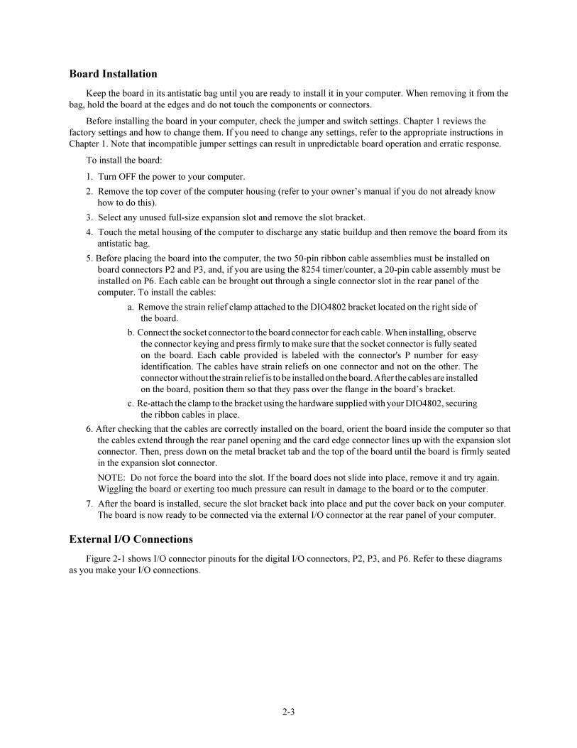
Figure 2-1 shows I/O connector pinouts for the digital I/O connectors, P2, P3, and P6. Refer to these diagramsas you make your I/O connections.

2-4
1 9 2 0
1 7 1 8
1 5 1 6
1 3 1 4
11 1 2
9 1 0
7 8
5 6
3 4
1 2EXT CLK 0
EXT GATE 0
T/C OUT 0
EXT CLK 1
EXT GATE 1
T/C OUT 1
EXT CLK 2
T/C OUT 2
EXT GATE 2
DIGITAL GND
DIGITAL GND
DIGITAL GND
DIGITAL GND
DIGITAL GND
DIGITAL GND
DIGITAL GND
DIGITAL GND
DIGITAL GND
DIGITAL GND
DIGITAL GND
P6
3 9 4 0
3 7 3 8
3 5 3 6
3 3 3 4
3 1 3 2
2 9 3 0
2 7 2 8
2 5 2 6
2 3 2 4
2 1 2 2
1 9 2 0
1 7 1 8
1 5 1 6
1 3 1 4
11 1 2
9 1 0
7 8
5 6
3 4
1 2
4 9 5 0
4 7 4 8
4 5 4 6
4 3 4 4
4 1 4 2
PC7
PC6
PC5
PC4
PC3
PC2
PC1
PC0
PB7
PB6
PB5
PB4
PB3
PB2
PB1
PB0
PA7
PA6
PA5
PA4
PA3
PA2
PA1
PA0
+5 VOLTS
EXTINT1
DIGITAL GND
DIGITAL GND
DIGITAL GND
DIGITAL GND
DIGITAL GND
DIGITAL GND
DIGITAL GND
DIGITAL GND
DIGITAL GND
DIGITAL GND
DIGITAL GND
DIGITAL GND
DIGITAL GND
DIGITAL GND
DIGITAL GND
DIGITAL GND
DIGITAL GND
DIGITAL GND
DIGITAL GND
DIGITAL GND
DIGITAL GND
DIGITAL GND
DIGITAL GND
DIGITAL GND
P2
3 9 4 0
3 7 3 8
3 5 3 6
3 3 3 4
3 1 3 2
2 9 3 0
2 7 2 8
2 5 2 6
2 3 2 4
2 1 2 2
1 9 2 0
1 7 1 8
1 5 1 6
1 3 1 4
11 1 2
9 1 0
7 8
5 6
3 4
1 2
4 9 5 0
4 7 4 8
4 5 4 6
4 3 4 4
4 1 4 2
PC7
PC6
PC5
PC4
PC3
PC2
PC1
PC0
PB7
PB6
PB5
PB4
PB3
PB2
PB1
PB0
PA7
PA6
PA5
PA4
PA3
PA2
PA1
PA0
+5 VOLTS
EXTINT2
DIGITAL GND
DIGITAL GND
DIGITAL GND
DIGITAL GND
DIGITAL GND
DIGITAL GND
DIGITAL GND
DIGITAL GND
DIGITAL GND
DIGITAL GND
DIGITAL GND
DIGITAL GND
DIGITAL GND
DIGITAL GND
DIGITAL GND
DIGITAL GND
DIGITAL GND
DIGITAL GND
DIGITAL GND
DIGITAL GND
DIGITAL GND
DIGITAL GND
DIGITAL GND
DIGITAL GND
P3
Fig. 2-1 � P2, P3, and P6 I/O Connector Pin Assignments
Connecting the Digital I/O
The DIO4802 is designed for direct connection to industry standard opto-22 isolated I/O racks and systemmodules. Each digital I/O line has a digital ground, as shown in Figure 2-1. For all digital I/O connections, the highside of an external signal source or destination device is connected to the appropriate signal pin on the I/O connec-tor, and the low side is connected to the DIGITAL GND. A cable to provide direct connection to opto-22 systems,the XO50, is available as an accessory from RTD.
Connecting the Timer/Counter I/O
External connections to the timer/counters on the DIO4802 can be made by connecting the high side of theexternal device to the appropriate signal pin on I/O connector P6 and the low side to a P6 DIGITAL GND.
Connecting the External Interrupt
The DIO4802 can receive externally generated interrupt signals � EXTINT1, through I/O connector P2, pin 2;and EXTINT2, through I/O connector P3, pin 2 � and route them to an IRQ channel selected through software.Interrupt generation is enabled through software. When interrupts are enabled, a rising edge on the EXTINT linewill cause the selected IRQ line to go high, and the IRQ status bit will change from 0 to 1. The pulse applied to theEXTINT pin should have a duration of at least 100 nanoseconds.
Running the 4802DIAG Diagnostics Program
Now that your board is ready to use, you will want to try it out. An easy-to-use, menu-driven diagnosticsprogram, 4802DIAG, is included with your example software to help you verify your board�s operation. You canalso use this program to make sure that your current base address setting does not contend with another device.

3-1
CHAPTER 3
HARDWARE DESCRIPTION
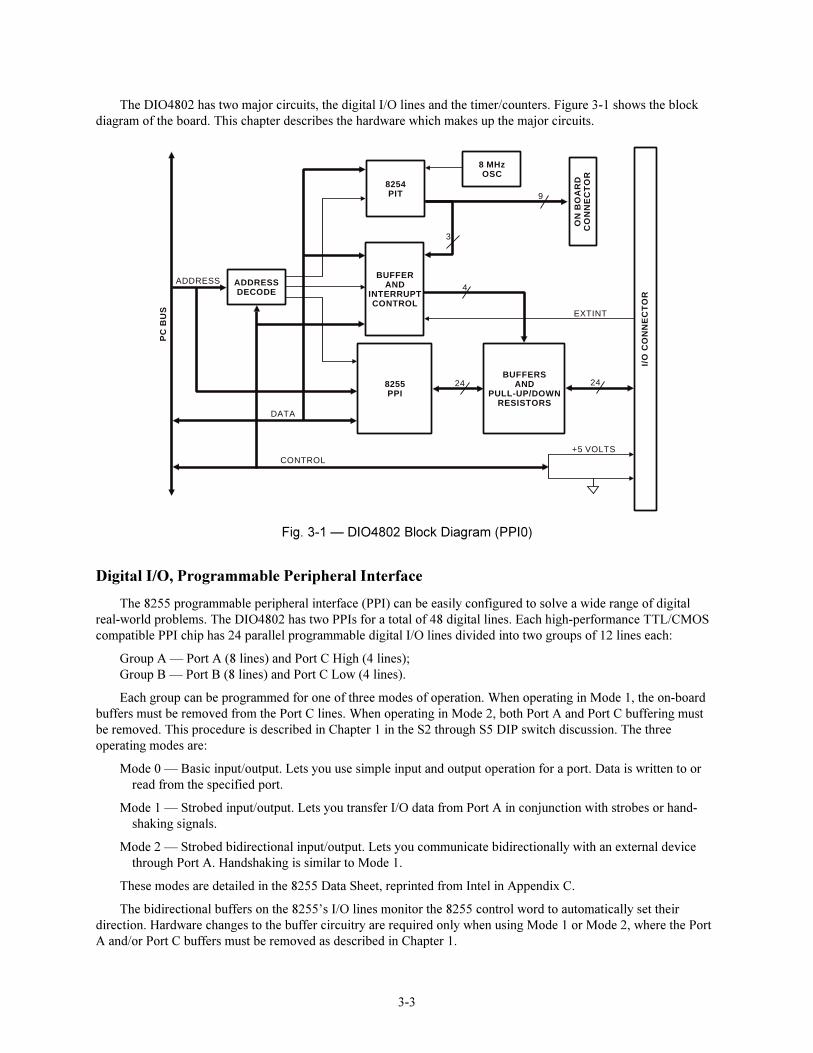
This chapter describes the features of the DIO4802 hardware.The major circuits are the digital I/O lines and the timer/counters.

3-2
3-3
The DIO4802 has two major circuits, the digital I/O lines and the timer/counters. Figure 3-1 shows the blockdiagram of the board. This chapter describes the hardware which makes up the major circuits.
+5 VOLTS
24
ADDRESSDECODE
BUFFERAND
INTERRUPTCONTROL
ADDRESS
DATA
CONTROL
PC
BU
S EXTINT
BUFFERSAND
PULL-UP/DOWNRESISTORS
8255PPI
24
4
8254PIT
8 MHzOSC
9
3
I/O
CO
NN
EC
TO
R
ON
BO
AR
DC
ON
NE
CT
OR
Fig. 3-1 � DIO4802 Block Diagram (PPI0)
Digital I/O, Programmable Peripheral Interface
The 8255 programmable peripheral interface (PPI) can be easily configured to solve a wide range of digitalreal-world problems. The DIO4802 has two PPIs for a total of 48 digital lines. Each high-performance TTL/CMOScompatible PPI chip has 24 parallel programmable digital I/O lines divided into two groups of 12 lines each:
Group A � Port A (8 lines) and Port C High (4 lines);Group B � Port B (8 lines) and Port C Low (4 lines).
Each group can be programmed for one of three modes of operation. When operating in Mode 1, the on-boardbuffers must be removed from the Port C lines. When operating in Mode 2, both Port A and Port C buffering mustbe removed. This procedure is described in Chapter 1 in the S2 through S5 DIP switch discussion. The threeoperating modes are:
Mode 0 � Basic input/output. Lets you use simple input and output operation for a port. Data is written to orread from the specified port.
Mode 1 � Strobed input/output. Lets you transfer I/O data from Port A in conjunction with strobes or hand-shaking signals.
Mode 2 � Strobed bidirectional input/output. Lets you communicate bidirectionally with an external devicethrough Port A. Handshaking is similar to Mode 1.
These modes are detailed in the 8255 Data Sheet, reprinted from Intel in Appendix C.
The bidirectional buffers on the 8255�s I/O lines monitor the 8255 control word to automatically set theirdirection. Hardware changes to the buffer circuitry are required only when using Mode 1 or Mode 2, where the PortA and/or Port C buffers must be removed as described in Chapter 1.
3-4
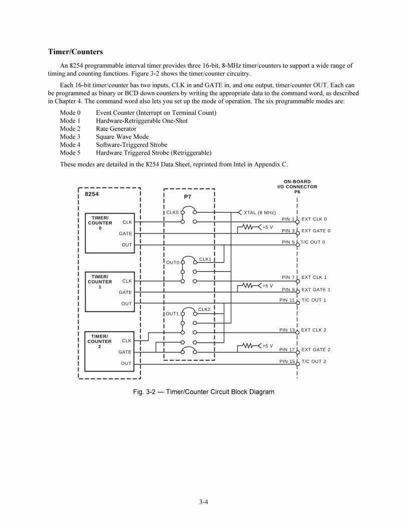
Timer/Counters
An 8254 programmable interval timer provides three 16-bit, 8-MHz timer/counters to support a wide range oftiming and counting functions. Figure 3-2 shows the timer/counter circuitry.
Each 16-bit timer/counter has two inputs, CLK in and GATE in, and one output, timer/counter OUT. Each canbe programmed as binary or BCD down counters by writing the appropriate data to the command word, as describedin Chapter 4. The command word also lets you set up the mode of operation. The six programmable modes are:
Mode 0 Event Counter (Interrupt on Terminal Count)Mode 1 Hardware-Retriggerable One-ShotMode 2 Rate GeneratorMode 3 Square Wave ModeMode 4 Software-Triggered StrobeMode 5 Hardware Triggered Strobe (Retriggerable)
These modes are detailed in the 8254 Data Sheet, reprinted from Intel in Appendix C.
CLK1
CLK2
CLK0
ON-BOARDI/O CONNECTOR
P6
PIN 17
PIN 7
PIN 11
8254
TIMER/COUNTER
0CLK
GATE
OUT
TIMER/COUNTER
1CLK
GATE
OUT
TIMER/COUNTER
2CLK
GATE
OUT
PIN 1
PIN 15
XTAL (8 MHz)
P7
+5 V
+5 V
+5 V
PIN 3
PIN 5
PIN 9
PIN 13
T/C OUT 0
OUT0
OUT1
EXT CLK 0
T/C OUT 1
EXT CLK 1
EXT GATE 2
T/C OUT 2
EXT CLK 2
EXT GATE 0
EXT GATE 1
Fig. 3-2 � Timer/Counter Circuit Block Diagram
4-1
CHAPTER 4
I/O MAPPING
This chapter provides a complete description of the I/O map forthe DIO4802, general programming information, and how to setand clear bits in a port.

4-2
4-3
Defining the I/O Map
The I/O map for the DIO4802 is shown in Table 4-1. As shown, the board occupies 16 consecutive I/O portlocations.
The base address (designated as BA) can be selected using DIP switch S1, located on the edge of the board, asdescribed in Chapter 1, Board Settings. This switch can be accessed without removing the board from the computer.The following sections describe the register contents of each address used in the I/O map.
Table 4-1: DIO4802 I/O Map
Register Description Read Function Write FunctionAddress *(Decimal)
8255 PPI0 Port A Read Port A digital input lines Program Port A digital output lines BA + 0
8255 PPI0 Port B Read Port B digital input lines Program Port B digital output lines BA + 1
8255 PPI0 Port C Read Port C digital input lines Program Port C digital output lines BA + 2
8255 PPI0 Control Word Reserved Program PPI0Õs configuration BA + 3
8255 PPI1 Port A Read Port A digital input lines Program Port A digital output lines BA + 4
8255 PPI1 Port B Read Port B digital input lines Program Port B digital output lines BA + 5
8255 PPI1 Port C Read Port C digital input lines Program Port C digital output lines BA + 6
8255 PPI1 Control Word Reserved Program PPI1Õs configuration BA + 7
8254 Timer/Counter 0 Read TC0 count value Load TC0 count register BA + 8
8254 Timer/Counter 1 Read TC1 count value Load TC1 count register BA + 9
8254 Timer/Counter 2 Read TC2 count value Load TC2 count register BA + 10
8254 Control Word Reseved Program control register BA + 11IRQ Status/IRQChannel/Source Select Read IRQ status
Program IRQ channel and source;enable IRQ BA + 12
Reset Board Reserved Resets board BA + 13
Clear IRQ Reserved Clears IRQ status bit BA + 14
Reserved Reserved Reserved BA + 15
* BA = Base Address
4-4
BA + 0: PPI0 Port A � Digital I/O (Read/Write)
Transfers PPI0�s 8-bit Port A digital input and digital output data between the board and an external device. Aread transfers data from the external device, through P2, and into PPI0 Port A; a write transfers the written data fromPort A through P2 to an external device.
BA + 1: PPI0 Port B � Digital I/O (Read/Write)
Transfers PPI0�s 8-bit Port B digital input and digital output data between the board and an external device. Aread transfers data from the external device, through P2, and into PPI0 Port B; a write transfers the written data fromPort B through P2 to an external device.
BA + 2: PPI0 Port C � Digital I/O (Read/Write)
Transfers PPI0�s two 4-bit Port C digital input and digital output data groups (Port C High and Port C Low)between the board and an external device. A read transfers data from the external device, through P2, and into PPI0Port C; a write transfers the written data from Port C through P2 to an external device.
BA + 3: 8255 PPI0 Control Word (Write Only)
D7 D6 D5 D4 D3 D2 D1 D0
Port C Lower0 = output1 = input
Port B0 = output1 = input
Mode Set Flag1 = active
Port C Upper0 = output1 = input
Port A0 = output1 = input
Group B
Mode Select00 = mode 001 = mode 110 = mode 2
Mode Select0 = mode 01 = mode 1
1 X X X X X X X
Group A
When bit 7 of this word is set to 1, a write programs the PPI0 configuration. The following table shows thecontrol words for the 16 possible Mode 0 Port I/O combinations.

4-5
Set/ResetFunction Bit0 = active
Bit Set/Reset0 = set bit to 01 = set bit to 1
Bit Select000 = PC0001 = PC1010 = PC2011 = PC3100 = PC4101 = PC5110 = PC6111 = PC7
D7 D6 D5 D4 D3 D2 D1 D0
Set/ResetFunction Bit
Set PC0X = don�t care
0 X X X 0 0 0 1
Sets PPI0 PC0 to 1:(written to BA +3)
For example, if you want to set PPI0 Port C bit 0 to 1, you would set up the control word so that bit 7 is 0; bits1, 2, and 3 are 0 (this selects PC0); and bit 0 is 1 (this sets PC0 to 1). The control word is set up like this:
Bit Select000 = PC0
D7 D6 D5 D4 D3 D2 D1 D0
When bit 7 of this word is set to 0, a write can be used to individually program the Port C lines.
�����3RUW�,�2�)ORZ�'LUHFWLRQ�DQG�&RQWURO�:RUGV��0RGH��
*URXS�$ *URXS�% &RQWURO�:RUG
3RUW�$3RUW�&8SSHU
3RUW�%3RUW�&/RZHU
%LQDU\ 'HFLPDO +H[
2XWSXW 2XWSXW 2XWSXW 2XWSXW ��������������� ��� ��
2XWSXW 2XWSXW 2XWSXW ,QSXW ��������������� ��� ��
2XWSXW 2XWSXW ,QSXW 2XWSXW ��������������� ��� ��
2XWSXW 2XWSXW ,QSXW ,QSXW ��������������� ��� ��
2XWSXW ,QSXW 2XWSXW 2XWSXW ��������������� ��� ��
2XWSXW ,QSXW 2XWSXW ,QSXW ��������������� ��� ��
2XWSXW ,QSXW ,QSXW 2XWSXW ��������������� ��� �$
2XWSXW ,QSXW ,QSXW ,QSXW ��������������� ��� �%
,QSXW 2XWSXW 2XWSXW 2XWSXW ��������������� ��� ��
,QSXW 2XWSXW 2XWSXW ,QSXW ��������������� ��� ��
,QSXW 2XWSXW ,QSXW 2XWSXW ��������������� ��� ��
,QSXW 2XWSXW ,QSXW ,QSXW ��������������� ��� ��
,QSXW ,QSXW 2XWSXW 2XWSXW ��������������� ��� ��
,QSXW ,QSXW 2XWSXW ,QSXW ��������������� ��� ��
,QSXW ,QSXW ,QSXW 2XWSXW ��������������� ��� �$
,QSXW ,QSXW ,QSXW ,QSXW ��������������� ��� �%

4-6
BA + 4: PPI1 Port A � Digital I/O (Read/Write)
Transfers PPI1�s 8-bit Port A digital input and digital output data between the board and an external device. Aread transfers data from the external device, through P3, and into PPI1 Port A; a write transfers the written data fromPort A through P3 to an external device.
BA + 5: PPI1 Port B � Digital I/O (Read/Write)
Transfers PPI1�s 8-bit Port B digital input and digital output data between the board and an external device. Aread transfers data from the external device, through P3, and into PPI1 Port B; a write transfers the written data fromPort B through P3 to an external device.
BA + 6: PPI1 Port C � Digital I/O (Read/Write)
Transfers PPI1�s two 4-bit Port C digital input and digital output data groups (Port C High and Port C Low)between the board and an external device. A read transfers data from the external device, through P3, and into PPI1Port C; a write transfers the written data from Port C through P3 to an external device.
BA + 7: 8255 PPI1 Control Word (Write Only)
When bit 7 of this word is set to 1, a write programs the PPI1 configuration. The following table shows thecontrol words for the 16 possible Mode 0 Port I/O combinations.
D7 D6 D5 D4 D3 D2 D1 D0
Port C Lower0 = output1 = input
Port B0 = output1 = input
Mode Set Flag1 = active
Port C Upper0 = output1 = input
Port A0 = output1 = input
Group B
Mode Select00 = mode 001 = mode 110 = mode 2
Mode Select0 = mode 01 = mode 1
1 X X X X X X X
Group A
4-7
D7 D6 D5 D4 D3 D2 D1 D0
Set/ResetFunction Bit0 = active
Bit Set/Reset0 = set bit to 01 = set bit to 1
Bit Select000 = PC0001 = PC1010 = PC2011 = PC3100 = PC4101 = PC5110 = PC6111 = PC7
D7 D6 D5 D4 D3 D2 D1 D0
Set/ResetFunction Bit
Set PC0X = don�t care
0 X X X 0 0 0 1
Sets PPI1 PC0 to 1:(written to BA +7)
Bit Select000 = PC0
When bit 7 of this word is set to 0, a write can be used to individually program the Port C lines.
For example, if you want to set PPI1 Port C bit 0 to 1, you would set up the control word so that bit 7 is 0; bits1, 2, and 3 are 0 (this selects PC0); and bit 0 is 1 (this sets PC0 to 1). The control word is set up like this:
�����3RUW�,�2�)ORZ�'LUHFWLRQ�DQG�&RQWURO�:RUGV��0RGH��
*URXS�$ *URXS�% &RQWURO�:RUG
3RUW�$3RUW�&8SSHU
3RUW�%3RUW�&/RZHU
%LQDU\ 'HFLPDO +H[
2XWSXW 2XWSXW 2XWSXW 2XWSXW ��������������� ��� ��
2XWSXW 2XWSXW 2XWSXW ,QSXW ��������������� ��� ��
2XWSXW 2XWSXW ,QSXW 2XWSXW ��������������� ��� ��
2XWSXW 2XWSXW ,QSXW ,QSXW ��������������� ��� ��
2XWSXW ,QSXW 2XWSXW 2XWSXW ��������������� ��� ��
2XWSXW ,QSXW 2XWSXW ,QSXW ��������������� ��� ��
2XWSXW ,QSXW ,QSXW 2XWSXW ��������������� ��� �$
2XWSXW ,QSXW ,QSXW ,QSXW ��������������� ��� �%
,QSXW 2XWSXW 2XWSXW 2XWSXW ��������������� ��� ��
,QSXW 2XWSXW 2XWSXW ,QSXW ��������������� ��� ��
,QSXW 2XWSXW ,QSXW 2XWSXW ��������������� ��� ��
,QSXW 2XWSXW ,QSXW ,QSXW ��������������� ��� ��
,QSXW ,QSXW 2XWSXW 2XWSXW ��������������� ��� ��
,QSXW ,QSXW 2XWSXW ,QSXW ��������������� ��� ��
,QSXW ,QSXW ,QSXW 2XWSXW ��������������� ��� �$
,QSXW ,QSXW ,QSXW ,QSXW ��������������� ��� �%

4-8
BA + 8: 8254 Timer/Counter 0 (Read/Write)
This address is used to read/write timer/counter 0. A read shows the count in the counter, and a write loads thecounter with a new value. Counting begins as soon as the count is loaded.
BA + 9: 8254 Timer/Counter 1 (Read/Write)
This address is used to read/write timer/counter 1. A read shows the count in the counter, and a write loads thecounter with a new value. Counting begins as soon as the count is loaded.
BA + 10: 8254 Timer/Counter 2 (Read/Write)
This address is used to read/write timer/counter 2. A read shows the count in the counter, and a write loads thecounter with a new value. Counting begins as soon as the count is loaded.
BA + 11: 8254 Timer/Counter Control Word (Write Only)
D7 D6 D5 D4 D3 D2 D1 D0
Counter Select00 = Counter 001 = Counter 110 = Counter 211 = read back setting
BCD/Binary0 = binary1 = BCD
Counter Mode Select000 = Mode 0, event count001 = Mode 1, programmable 1-shot010 = Mode 2, rate generator011 = Mode 3, square wave rate generator100 = Mode 4, software-triggered strobe101 = Mode 5, hardware-triggered strobe
Read/Load00 = latching operation01 = read/load LSB only10 = read/load MSB only11 = read/load LSB, then MSB
This address is used to write to the control register for the 8254. The control word is defined above.
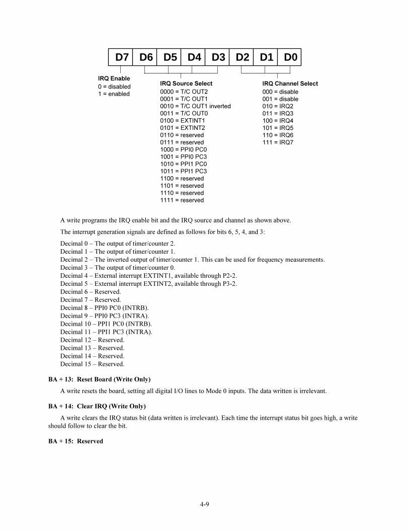
BA + 12: IRQ Status/IRQ Enable and Channel/Source Select (Read/Write)
D7 D6 D5 D4 D3 D2 D1 D0
IRQ Channel SelectIRQ Status0 = no IRQ1 = IRQ
IRQ Source Select
A read shows the IRQ status and lets you review the IRQ source and channel.
4-9
D7 D6 D5 D4 D3 D2 D1 D0
IRQ Channel Select000 = disable001 = disable010 = IRQ2011 = IRQ3100 = IRQ4101 = IRQ5110 = IRQ6111 = IRQ7
IRQ Enable0 = disabled1 = enabled
IRQ Source Select0000 = T/C OUT20001 = T/C OUT10010 = T/C OUT1 inverted0011 = T/C OUT00100 = EXTINT10101 = EXTINT20110 = reserved0111 = reserved1000 = PPI0 PC01001 = PPI0 PC31010 = PPI1 PC01011 = PPI1 PC31100 = reserved1101 = reserved1110 = reserved1111 = reserved
A write programs the IRQ enable bit and the IRQ source and channel as shown above.
The interrupt generation signals are defined as follows for bits 6, 5, 4, and 3:
Decimal 0 � The output of timer/counter 2.Decimal 1 � The output of timer/counter 1.Decimal 2 � The inverted output of timer/counter 1. This can be used for frequency measurements.Decimal 3 � The output of timer/counter 0.Decimal 4 � External interrupt EXTINT1, available through P2-2.Decimal 5 � External interrupt EXTINT2, available through P3-2.Decimal 6 � Reserved.Decimal 7 � Reserved.Decimal 8 � PPI0 PC0 (INTRB).Decimal 9 � PPI0 PC3 (INTRA).Decimal 10 � PPI1 PC0 (INTRB).Decimal 11 � PPI1 PC3 (INTRA).Decimal 12 � Reserved.Decimal 13 � Reserved.Decimal 14 � Reserved.Decimal 15 � Reserved.
BA + 13: Reset Board (Write Only)
A write resets the board, setting all digital I/O lines to Mode 0 inputs. The data written is irrelevant.
BA + 14: Clear IRQ (Write Only)
A write clears the IRQ status bit (data written is irrelevant). Each time the interrupt status bit goes high, a writeshould follow to clear the bit.
BA + 15: Reserved
4-10
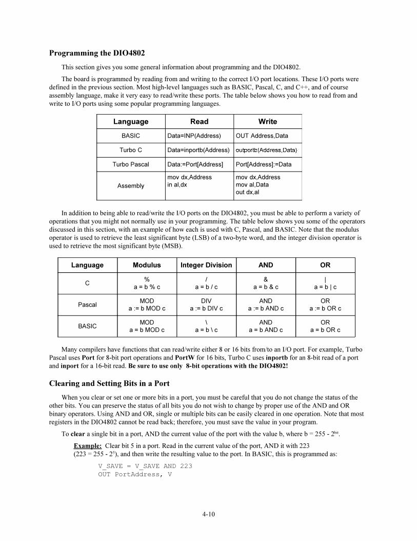
Programming the DIO4802
This section gives you some general information about programming and the DIO4802.
The board is programmed by reading from and writing to the correct I/O port locations. These I/O ports weredefined in the previous section. Most high-level languages such as BASIC, Pascal, C, and C++, and of courseassembly language, make it very easy to read/write these ports. The table below shows you how to read from andwrite to I/O ports using some popular programming languages.
In addition to being able to read/write the I/O ports on the DIO4802, you must be able to perform a variety ofoperations that you might not normally use in your programming. The table below shows you some of the operatorsdiscussed in this section, with an example of how each is used with C, Pascal, and BASIC. Note that the modulusoperator is used to retrieve the least significant byte (LSB) of a two-byte word, and the integer division operator isused to retrieve the most significant byte (MSB).
Many compilers have functions that can read/write either 8 or 16 bits from/to an I/O port. For example, TurboPascal uses Port for 8-bit port operations and PortW for 16 bits, Turbo C uses inportb for an 8-bit read of a portand inport for a 16-bit read. Be sure to use only 8-bit operations with the DIO4802!
Clearing and Setting Bits in a Port
When you clear or set one or more bits in a port, you must be careful that you do not change the status of theother bits. You can preserve the status of all bits you do not wish to change by proper use of the AND and ORbinary operators. Using AND and OR, single or multiple bits can be easily cleared in one operation. Note that mostregisters in the DIO4802 cannot be read back; therefore, you must save the value in your program.
To clear a single bit in a port, AND the current value of the port with the value b, where b = 255 - 2bit.
Example: Clear bit 5 in a port. Read in the current value of the port, AND it with 223(223 = 255 - 25), and then write the resulting value to the port. In BASIC, this is programmed as:
V_SAVE = V_SAVE AND 223OUT PortAddress, V
/DQJXDJH 5HDG :ULWH
%$6,& 'DWD ,13�$GGUHVV� 287�$GGUHVV�'DWD
7XUER�& 'DWD LQSRUWE�$GGUHVV� RXWSRUWE�$GGUHVV�'DWD�
7XUER�3DVFDO 'DWD� 3RUW>$GGUHVV@ 3RUW>$GGUHVV@� 'DWD
$VVHPEO\PRY�G[�$GGUHVVLQ�DO�G[
PRY�G[�$GGUHVVPRY�DO�'DWDRXW�G[�DO
/DQJXDJH 0RGXOXV ,QWHJHU�'LYLVLRQ $1' 25
&�
D� �E���F�
D� �E���F
D� �E��F_
D� �E�_�F
3DVFDO02'
D�� �E�02'�F',9
D�� �E�',9�F$1'
D�� �E�$1'�F25
D�� �E�25�F
%$6,&02'
D� �E�02'�F?
D� �E�?�F$1'
D� �E�$1'�F25
D� �E�25�F
4-11
To set a single bit in a port, OR the current value of the port with the value b, where b = 2bit.
Example: Set bit 3 in a port. Read in the current value of the port, OR it with 8 (8 = 23), and thenwrite the resulting value to the port. In Pascal, this is programmed as:
V_Save = V_Save OR 8;Port[PortAddress] := V_Save;
Setting or clearing more than one bit at a time is accomplished just as easily. To clear multiple bits in a port,AND the current value of the port with the value b, where b = 255 - (the sum of the values of the bits to be cleared).Note that the bits do not have to be consecutive.
Example: Clear bits 2, 4, and 6 in a port. Read in the current value of the port, AND it with 171(171 = 255 - 22 - 24 - 26), and then write the resulting value to the port. In C, this is programmedas:
v_save = v_save & 171;outportb(port_address, v_save);
To set multiple bits in a port, OR the current value of the port with the value b, where b = the sum of theindividual bits to be set. Note that the bits to be set do not have to be consecutive.
Example: Set bits 3, 5, and 7 in a port. Read in the current value of the port, OR it with 168(168 = 23 + 25 + 27), and then write the resulting value back to the port. In assembly language, thisis programmed as:
mov al, v_saveor al, 168mov dx, PortAddressout dx, al
Often, assigning a range of bits is a mixture of setting and clearing operations. You can set or clear each bitindividually or use a faster method of first clearing all the bits in the range then setting only those bits that must beset using the method shown above for setting multiple bits in a port. The following example shows how this two-step operation is done.
Example: Assign bits 3, 4, and 5 in a port to 101 (bits 3 and 5 set, bit 4 cleared). First, read in theport and clear bits 3, 4, and 5 by ANDing them with 199. Then set bits 3 and 5 by ORing themwith 40, and finally write the resulting value back to the port. In C, this is programmed as:
v_save = v_save & 199;v_save = v_save | 40;outportb(port_address, v_save);
A final note: Don�t be intimidated by the binary operators AND and OR and try to use operators for which youhave a better intuition. For instance, if you are tempted to use addition and subtraction to set and clear bits in placeof the methods shown above, DON�T! Addition and subtraction may seem logical, but they will not work if you tryto clear a bit that is already clear or set a bit that is already set. For example, you might think that to set bit 5 of aport, you simply need to read in the port, add 32 (25) to that value, and then write the resulting value back to the port.This works fine if bit 5 is not already set. But, what happens when bit 5 is already set? Bits 0 to 4 will be unaffectedand we can�t say for sure what happens to bits 6 and 7, but we can say for sure that bit 5 ends up cleared instead ofbeing set. A similar problem happens when you use subtraction to clear a bit in place of the method shown above.

4-12
5-1
CHAPTER 5
DIGITAL I/O
This chapter explains the digital I/O circuitry on the DIO4802.

5-2
5-3
The DIO4802 has 48 buffered TTL/CMOS digital I/O lines available for digital control applications. Theselines are grouped in two 24-bit 8255 PPIs. The 8255 data sheet is included in Appendix C.
Initializing the 8255 PPIs
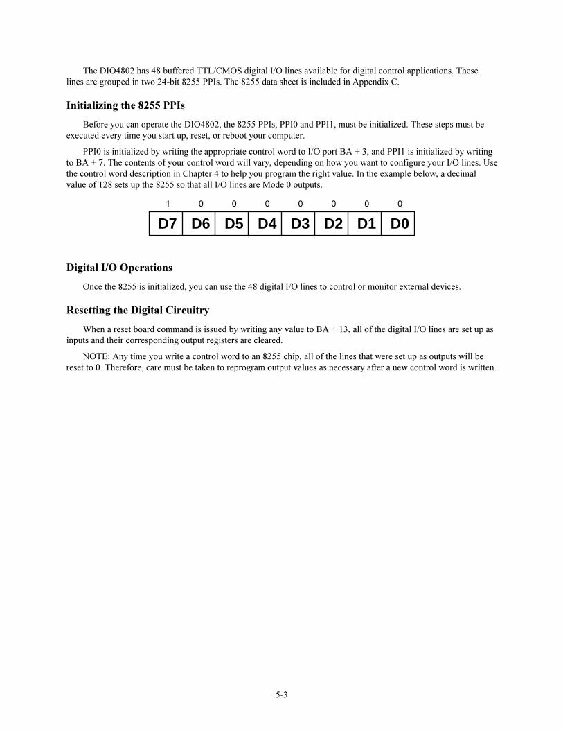
Before you can operate the DIO4802, the 8255 PPIs, PPI0 and PPI1, must be initialized. These steps must beexecuted every time you start up, reset, or reboot your computer.
PPI0 is initialized by writing the appropriate control word to I/O port BA + 3, and PPI1 is initialized by writingto BA + 7. The contents of your control word will vary, depending on how you want to configure your I/O lines. Usethe control word description in Chapter 4 to help you program the right value. In the example below, a decimalvalue of 128 sets up the 8255 so that all I/O lines are Mode 0 outputs.
D7 D6 D5 D4 D3 D2 D1 D0
1 0 0 0 0 0 0 0
Digital I/O Operations
Once the 8255 is initialized, you can use the 48 digital I/O lines to control or monitor external devices.
Resetting the Digital Circuitry
When a reset board command is issued by writing any value to BA + 13, all of the digital I/O lines are set up asinputs and their corresponding output registers are cleared.
NOTE: Any time you write a control word to an 8255 chip, all of the lines that were set up as outputs will bereset to 0. Therefore, care must be taken to reprogram output values as necessary after a new control word is written.

5-4
6-1
CHAPTER 6
TIMER/COUNTERS
This chapter explains the 8254 timer/counter circuit on theDIO4802.

6-2

6-3
An 8254 programmable interval timer provides three 16-bit, 8-MHz timers for timing and counting functionssuch as frequency measurement, event counting, and interrupts. These timer/counters can be configured in a numberof ways to support your application. Figure 6-1 shows a block diagram of the timer/counter circuitry.
CLK1
CLK2
CLK0
ON-BOARDI/O CONNECTOR
P6
PIN 17
PIN 7
PIN 11
8254
TIMER/COUNTER
0CLK
GATE
OUT
TIMER/COUNTER
1CLK
GATE
OUT
TIMER/COUNTER
2CLK
GATE
OUT
PIN 1
PIN 15
XTAL (8 MHz)
P7
+5 V
+5 V
+5 V
PIN 3
PIN 5
PIN 9
PIN 13
T/C OUT 0
OUT0
OUT1
EXT CLK 0
T/C OUT 1
EXT CLK 1
EXT GATE 2
T/C OUT 2
EXT CLK 2
EXT GATE 0
EXT GATE 1
Fig. 6-1 � 8254 Timer/Counter Circuit Block Diagram
Each timer/counter has two inputs, CLK in and GATE in, and one output, timer/counter OUT. They can beprogrammed as binary or BCD down counters by writing the appropriate data to the command word, as described inthe I/O map discussion in Chapter 4.
The timer/counter outputs are available at P6 where they can be used for interrupt generation, as an A/D trigger,or for timing and counting functions.
The timers can be programmed to operate in one of six modes, depending on your application. The followingparagraphs briefly describe each mode.
Mode 0, Event Counter (Interrupt on Terminal Count). This mode is typically used for event counting.While the timer/counter counts down, the output is low, and when the count is complete, it goes high. The outputstays high until a new Mode 0 control word is written to the timer/counter.
Mode 1, Hardware-Retriggerable One-Shot. The output is initially high and goes low on the clock pulsefollowing a trigger to begin the one-shot pulse. The output remains low until the count reaches 0, and then goes highand remains high until the clock pulse after the next trigger.
Mode 2, Rate Generator. This mode functions like a divide-by-N counter and is typically used to generate areal-time clock interrupt. The output is initially high, and when the count decrements to 1, the output goes low forone clock pulse. The output then goes high again, the timer/counter reloads the initial count, and the process isrepeated. This sequence continues indefinitely.
Mode 3, Square Wave Mode. Similar to Mode 2 except for the duty cycle output, this mode is typically usedfor baud rate generation. The output is initially high, and when the count decrements to one-half its initial count, theoutput goes low for the remainder of the count. The timer/counter reloads and the output goes high again. Thisprocess repeats indefinitely.

6-4
Mode 4, Software-Triggered Strobe. The output is initially high. When the initial count expires, the outputgoes low for one clock pulse and then goes high again. Counting is �triggered� by writing the initial count.
Mode 5, Hardware Triggered Strobe (Retriggerable). The output is initially high. Counting is triggered bythe rising edge of the gate input. When the initial count has expired, the output goes low for one clock pulse andthen goes high again.
Appendix C provides the 8254 data sheet.

7-1
CHAPTER 7
INTERRUPTS
This chapter explains programmable interrupts and basicinterrupt programming techniques.

7-2
7-3
Software Programmable Interrupts
The DIO4802 circuitry has 10 software selectable interrupt sources which can be selected at BA + 12, bits 3through 6, as described in Chapter 4.
To use these interrupts, an interrupt source must be selected at BA + 12, bits 3 through 6, an interrupt channelmust be enabled at BA + 12, bits 0 through 2, and the IRQ enable must be set high (BA + 12, bit 7).
Basic Programming For Interrupt Handling
What Is an Interrupt?
An interrupt is an event that causes the processor in your computer to temporarily halt its current process andexecute another routine. Upon completion of the new routine, control is returned to the original routine at the pointwhere its execution was interrupted.
Interrupts are very handy for dealing with asynchronous events (events that occur at less than regular intervals).Keyboard activity is a good example; your computer cannot predict when you might press a key and it would be awaste of processor time for it to do nothing while waiting for a keystroke to occur. Thus, the interrupt scheme isused and the processor proceeds with other tasks. Then, when a keystroke does occur, the keyboard �interrupts� theprocessor, and the processor gets the keyboard data, places it in memory, and then returns to what it was doingbefore it was interrupted. Other common devices that use interrupts are modems, disk drives, and mice.
Your DIO4802 can interrupt the processor when a variety of conditions are met. By using these interrupts, youcan write software that effectively deals with real world events.
Interrupt Request Lines
To allow different peripheral devices to generate interrupts on the same computer, the PC bus has eight differentinterrupt request (IRQ) lines. A transition from low to high on one of these lines generates an interrupt requestwhich is handled by the PC�s interrupt controller. The interrupt controller checks to see if interrupts are to beacknowledged from that IRQ and, if another interrupt is already in progress, it decides if the new request shouldsupersede the one in progress or if it has to wait until the one in progress is done. This prioritizing allows aninterrupt to be interrupted if the second request has a higher priority. The priority level is based on the number of theIRQ; IRQ0 has the highest priority, IRQ1 is second-highest, and so on through IRQ7, which has the lowest. Many ofthe IRQs are used by the standard system resources. IRQ0 is used by the system timer, IRQ1 is used by the key-board, IRQ3 by COM2, IRQ4 by COM1, and IRQ6 by the disk drives. Therefore, it is important for you to knowwhich IRQ lines are available in your system for use by the module.
8259 Programmable Interrupt Controller
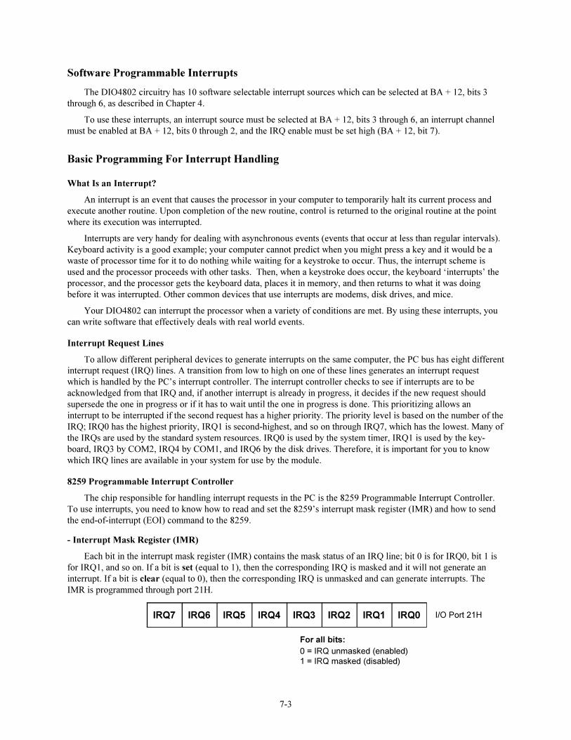
The chip responsible for handling interrupt requests in the PC is the 8259 Programmable Interrupt Controller.To use interrupts, you need to know how to read and set the 8259�s interrupt mask register (IMR) and how to sendthe end-of-interrupt (EOI) command to the 8259.
- Interrupt Mask Register (IMR)
Each bit in the interrupt mask register (IMR) contains the mask status of an IRQ line; bit 0 is for IRQ0, bit 1 isfor IRQ1, and so on. If a bit is set (equal to 1), then the corresponding IRQ is masked and it will not generate aninterrupt. If a bit is clear (equal to 0), then the corresponding IRQ is unmasked and can generate interrupts. TheIMR is programmed through port 21H.
For all bits:0 = IRQ unmasked (enabled)1 = IRQ masked (disabled)
I/O Port 21H,54� ,54� ,54� ,54� ,54� ,54� ,54� ,54�
7-4
- End-of-Interrupt (EOI) Command
After an interrupt service routine is complete, the 8259 interrupt controller must be notified. This is done bywriting the value 20H to I/O port 20H.
What Exactly Happens When an Interrupt Occurs?
Understanding the sequence of events when an interrupt is triggered is necessary to properly write softwareinterrupt handlers. When an interrupt request line is driven high by a peripheral device (such as the DIO4802), theinterrupt controller checks to see if interrupts are enabled for that IRQ, and then checks to see if other interrupts areactive or requested and determines which interrupt has priority. The interrupt controller then interrupts the proces-sor. The current code segment (CS), instruction pointer (IP), and flags are pushed on the stack for storage, and a newCS and IP are loaded from a table that exists in the lowest 1024 bytes of memory. This table is referred to as theinterrupt vector table and each entry is called an interrupt vector. Once the new CS and IP are loaded from theinterrupt vector table, the processor begins executing the code located at CS:IP. When the interrupt routine iscompleted, the CS, IP, and flags that were pushed on the stack when the interrupt occurred are now popped from thestack and execution resumes from the point where it was interrupted.
Using Interrupts in Your Programs
Adding interrupts to your software is not as difficult as it may seem, and what they add in terms of performanceis often worth the effort. Note, however, that although it is not that hard to use interrupts, the smallest mistake willoften lead to a system hang that requires a reboot. This can be both frustrating and time-consuming. But, after a fewtries, you�ll get the bugs worked out and enjoy the benefits of properly executed interrupts. In addition to reading thefollowing paragraphs, study the INTRPTS source code included on your DIO4802 program disk for a betterunderstanding of interrupt program development.
Writing an Interrupt Service Routine (ISR)
The first step in adding interrupts to your software is to write the interrupt service routine (ISR). This is theroutine that will automatically be executed each time an interrupt request occurs on the specified IRQ. An ISR isdifferent than standard routines that you write. First, on entrance, the processor registers should be pushed onto thestack BEFORE you do anything else. Second, just before exiting your ISR, you must clear the interrupt status flagof the DIO4802 and write an end-of-interrupt command to the 8259 controller. Finally, when exiting the ISR, inaddition to popping all the registers you pushed on entrance, you must use the IRET instruction and not a plainRET. The IRET automatically pops the flags, CS, and IP that were pushed when the interrupt was called.
If you find yourself intimidated by interrupt programming, take heart. Most Pascal and C compilers allow youto identify a procedure (function) as an interrupt type and will automatically add these instructions to your ISR, withone important exception: most compilers do not automatically add the end-of-interrupt command to the procedure;you must do this yourself. Other than this and the few exceptions discussed below, you can write your ISR just likeany other routine. It can call other functions and procedures in your program and it can access global data. If you arewriting your first ISR, we recommend that you stick to the basics; just something that will convince you that itworks, such as incrementing a global variable.
NOTE: If you are writing an ISR using assembly language, you are responsible for pushing and poppingregisters and using IRET instead of RET.
There are a few cautions you must consider when writing your ISR. The most important is, do not use anyDOS functions or routines that call DOS functions from within an ISR. DOS is not reentrant; that is, a DOSfunction cannot call itself. In typical programming, this will not happen because of the way DOS is written. Butwhat about when using interrupts? Then, you could have a situation such as this in your program. If DOS function Xis being executed when an interrupt occurs and the interrupt routine makes a call to DOS function X, then functionX is essentially being called while it is already active. Such a reentrancy attempt spells disaster because DOSfunctions are not written to support it. This is a complex concept and you do not need to understand it. Just makesure that you do not call any DOS functions from within your ISR. The one wrinkle is that, unfortunately, it is notobvious which library routines included with your compiler use DOS functions. A rule of thumb is that routineswhich write to the screen, or check the status of or read the keyboard, and any disk I/O routines use DOS and shouldbe avoided in your ISR.
7-5
The same problem of reentrancy exists for many floating point emulators as well, meaning you may have toavoid floating point (real) math in your ISR.
Note that the problem of reentrancy exists, no matter what programming language you are using. Even if youare writing your ISR in assembly language, DOS and many floating point emulators are not reentrant. Of course,there are ways around this problem, such as those which involve checking to see if any DOS functions are currentlyactive when your ISR is called, but such solutions are well beyond the scope of this discussion.
The second major concern when writing your ISR is to make it as short as possible in terms of execution time.Spending long periods of time in your ISR may mean that other important interrupts are being ignored. Also, if youspend too long in your ISR, it may be called again before you have completed handling the first run. This often leadsto a hang that requires a reboot.
Your ISR should have this structure:
� Push any processor registers used in your ISR. Most C and Pascal interrupt routines automatically do this foryou.
� Put the body of your routine here.� Clear the software programmable interrupt status flag by writing to BA + 14.� Issue the EOI command to the 8259 interrupt controller by writing 20H to port 20H.� Pop all registers pushed on entrance. Most C and Pascal interrupt routines automatically do this for you.
The following C and Pascal examples show what the shell of your ISR should be like.
In C:
void interrupt ISR(void){
/* Your code goes here. Do not use any DOS functions! */outportb(BaseAddress + 14, 0); /* Clear IRQ */outportb(0x20, 0x20); /* Send EOI command to 8259 */
}
In Pascal:
Procedure ISR; Interrupt;begin
{ Your code goes here. Do not use any DOS functions! }Port[BaseAddress + 14] := 0; { Clear IRQ }
Port[$20] := $20; { Send EOI command to 8259 }end;
Saving the Startup Interrupt Mask Register (IMR) and Interrupt Vector
The next step after writing the ISR is to save the startup state of the interrupt mask register and the interruptvector that you will be using. The IMR is located at I/O port 21H. The interrupt vector you will be using is locatedin the interrupt vector table which is simply an array of 256-bit (4-byte) pointers and is located in the first 1024bytes of memory (Segment = 0, Offset = 0). You can read this value directly, but it is a better practice to use DOSfunction 35H (get interrupt vector). Most C and Pascal compilers provide a library routine for reading the value of avector. The vectors for the hardware interrupts are vectors 8 through 15, where IRQ0 uses vector 8, IRQ1 usesvector 9, and so on. Thus, if the DIO4802 will be using IRQ3, you should save the value of interrupt vector 11.
Before you install your ISR, temporarily mask out the IRQ you will be using. This prevents the IRQ fromrequesting an interrupt while you are installing and initializing your ISR. To mask the IRQ, read in the current IMRat I/O port 21H and set the bit that corresponds to your IRQ (remember, setting a bit disables interrupts on that IRQwhile clearing a bit enables them). The IMR is arranged so that bit 0 is for IRQ0, bit 1 is for IRQ1, and so on. Seethe paragraph entitled Interrupt Mask Register (IMR) earlier in this chapter for help in determining your IRQ�s bit.After setting the bit, write the new value to I/O port 21H.
7-6
With the startup IMR saved and the interrupts on your IRQ temporarily disabled, you can assign the interruptvector to point to your ISR. Again, you can overwrite the appropriate entry in the vector table with a direct memorywrite, but this is a bad practice. Instead, use either DOS function 25H (set interrupt vector) or, if your compilerprovides it, the library routine for setting an interrupt vector. Remember that vector 8 is for IRQ0, vector 9 is forIRQ1, and so on.
If you need to program the source of your interrupts, do that next. For example, if you are using the program-mable interval timer to generate interrupts, you must program it to run in the proper mode and at the proper rate.
Finally, clear the bit in the IMR for the IRQ you are using. This enables interrupts on the IRQ.
Restoring the Startup IMR and Interrupt Vector
Before exiting your program, you must restore the interrupt mask register and interrupt vectors to the state theywere in when your program started. To restore the IMR, write the value that was saved when your program startedto I/O port 21H. Restore the interrupt vector that was saved at startup with either DOS function 35H (get interruptvector), or use the library routine supplied with your compiler. Performing these two steps will guarantee that theinterrupt status of your computer is the same after running your program as it was before your program startedrunning.
Common Interrupt Mistakes
� Remember that hardware interrupts are numbered 8 through 15, even though the corresponding IRQs arenumbered 0 through 7.
� Two of the most common mistakes when writing an ISR are forgetting to clear the interrupt status of theDIO4802 and forgetting to issue the EOI command to the 8259 interrupt controller before exiting the ISR.

A-1
APPENDIX A
DIO4802 SPECIFICATIONS

A-2
A-3
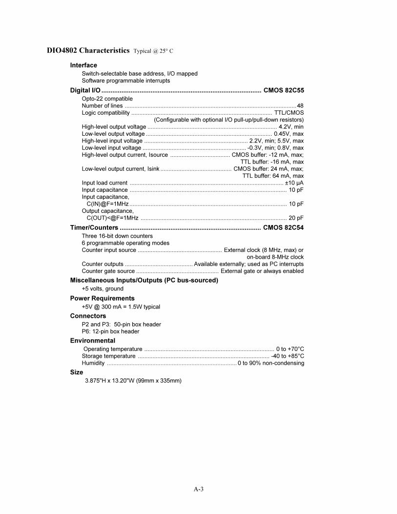
DIO4802 Characteristics Typical @ 25° C
InterfaceSwitch-selectable base address, I/O mappedSoftware programmable interrupts
Digital I/O ........................................................................................ CMOS 82C55Opto-22 compatibleNumber of lines ..........................................................................................................48Logic compatibility ....................................................................................... TTL/CMOS
(Configurable with optional I/O pull-up/pull-down resistors)High-level output voltage ................................................................................ 4.2V, minLow-level output voltage .............................................................................. 0.45V, maxHigh-level input voltage ................................................................ 2.2V, min; 5.5V, maxLow-level input voltage ................................................................ -0.3V, min; 0.8V, maxHigh-level output current, Isource ..................................... CMOS buffer: -12 mA, max;
TTL buffer: -16 mA, maxLow-level output current, Isink ............................................ CMOS buffer: 24 mA, max;
TTL buffer: 64 mA, maxInput load current ............................................................................................... ±10 µAInput capacitance ................................................................................................. 10 pFInput capacitance, C(IN)@F=1MHz ................................................................................................. 10 pFOutput capacitance, C(OUT)<@F=1MHz .......................................................................................... 20 pF
Timer/Counters .............................................................................. CMOS 82C54Three 16-bit down counters6 programmable operating modesCounter input source .................................................... External clock (8 MHz, max) or
on-board 8-MHz clockCounter outputs .......................................... Available externally; used as PC interruptsCounter gate source ................................................... External gate or always enabled
Miscellaneous Inputs/Outputs (PC bus-sourced)+5 volts, ground
Power Requirements+5V @ 300 mA = 1.5W typical
ConnectorsP2 and P3: 50-pin box headerP6: 12-pin box header
Environmental Operating temperature ................................................................................ 0 to +70°CStorage temperature ................................................................................. -40 to +85°CHumidity ................................................................................ 0 to 90% non-condensing
Size 3.875"H x 13.20"W (99mm x 335mm)

A-4

B-1
APPENDIX B
CONNECTOR PIN ASSIGNMENTS

B-2
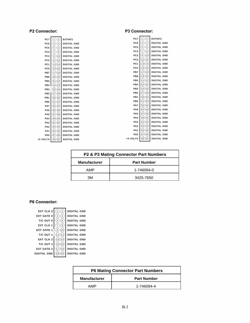
B-3
P2 Connector:
3 9 4 0
3 7 3 8
3 5 3 6
3 3 3 4
3 1 3 2
2 9 3 0
2 7 2 8
2 5 2 6
2 3 2 4
2 1 2 2
1 9 2 0
1 7 1 8
1 5 1 6
1 3 1 4
11 1 2
9 1 0
7 8
5 6
3 4
1 2
4 9 5 0
4 7 4 8
4 5 4 6
4 3 4 4
4 1 4 2
PC7
PC6
PC5
PC4
PC3
PC2
PC1
PC0
PB7
PB6
PB5
PB4
PB3
PB2
PB1
PB0
PA7
PA6
PA5
PA4
PA3
PA2
PA1
PA0
+5 VOLTS
EXTINT1
DIGITAL GND
DIGITAL GND
DIGITAL GND
DIGITAL GND
DIGITAL GND
DIGITAL GND
DIGITAL GND
DIGITAL GND
DIGITAL GND
DIGITAL GND
DIGITAL GND
DIGITAL GND
DIGITAL GND
DIGITAL GND
DIGITAL GND
DIGITAL GND
DIGITAL GND
DIGITAL GND
DIGITAL GND
DIGITAL GND
DIGITAL GND
DIGITAL GND
DIGITAL GND
DIGITAL GND
3 9 4 0
3 7 3 8
3 5 3 6
3 3 3 4
3 1 3 2
2 9 3 0
2 7 2 8
2 5 2 6
2 3 2 4
2 1 2 2
1 9 2 0
1 7 1 8
1 5 1 6
1 3 1 4
11 1 2
9 1 0
7 8
5 6
3 4
1 2
4 9 5 0
4 7 4 8
4 5 4 6
4 3 4 4
4 1 4 2
PC7
PC6
PC5
PC4
PC3
PC2
PC1
PC0
PB7
PB6
PB5
PB4
PB3
PB2
PB1
PB0
PA7
PA6
PA5
PA4
PA3
PA2
PA1
PA0
+5 VOLTS
EXTINT2
DIGITAL GND
DIGITAL GND
DIGITAL GND
DIGITAL GND
DIGITAL GND
DIGITAL GND
DIGITAL GND
DIGITAL GND
DIGITAL GND
DIGITAL GND
DIGITAL GND
DIGITAL GND
DIGITAL GND
DIGITAL GND
DIGITAL GND
DIGITAL GND
DIGITAL GND
DIGITAL GND
DIGITAL GND
DIGITAL GND
DIGITAL GND
DIGITAL GND
DIGITAL GND
DIGITAL GND
P3 Connector:
P6 Connector:
1 9 2 0
1 7 1 8
1 5 1 6
1 3 1 4
11 1 2
9 1 0
7 8
5 6
3 4
1 2EXT CLK 0
EXT GATE 0
T/C OUT 0
EXT CLK 1
EXT GATE 1
T/C OUT 1
EXT CLK 2
T/C OUT 2
EXT GATE 2
DIGITAL GND
DIGITAL GND
DIGITAL GND
DIGITAL GND
DIGITAL GND
DIGITAL GND
DIGITAL GND
DIGITAL GND
DIGITAL GND
DIGITAL GND
DIGITAL GND
P2 & P3 Mating Connector Part Numbers
Manufacturer Part Number
AMP 1-746094-0
3M 3425-7650
P6 Mating Connector Part Numbers
Manufacturer Part Number
AMP 1-746094-4

B-4

APPENDIX C
COMPONENT DATA SHEETS
C-1


Intel 82C55A Programmable Peripheral InterfaceData Sheet Reprint


Intel 82C54 Programmable Interval TimerData Sheet Reprint


D-1
APPENDIX D
WARRANTY

D-2

D-3
LIMITED WARRANTY
Real Time Devices, Inc. warrants the hardware and software products it manufactures and produces to be freefrom defects in materials and workmanship for one year following the date of shipment from REAL TIME DE-VICES. This warranty is limited to the original purchaser of product and is not transferable.
During the one year warranty period, REAL TIME DEVICES will repair or replace, at its option, any defectiveproducts or parts at no additional charge, provided that the product is returned, shipping prepaid, to REAL TIMEDEVICES. All replaced parts and products become the property of REAL TIME DEVICES. Before returning anyproduct for repair, customers are required to contact the factory for an RMA number.
THIS LIMITED WARRANTY DOES NOT EXTEND TO ANY PRODUCTS WHICH HAVE BEEN DAM-AGED AS A RESULT OF ACCIDENT, MISUSE, ABUSE (such as: use of incorrect input voltages, improper orinsufficient ventilation, failure to follow the operating instructions that are provided by REAL TIME DEVICES,�acts of God� or other contingencies beyond the control of REAL TIME DEVICES), OR AS A RESULT OFSERVICE OR MODIFICATION BY ANYONE OTHER THAN REAL TIME DEVICES. EXCEPT AS EX-PRESSLY SET FORTH ABOVE, NO OTHER WARRANTIES ARE EXPRESSED OR IMPLIED, INCLUDING,BUT NOT LIMITED TO, ANY IMPLIED WARRANTIES OF MERCHANTABILITY AND FITNESS FOR APARTICULAR PURPOSE, AND REAL TIME DEVICES EXPRESSLY DISCLAIMS ALL WARRANTIES NOTSTATED HEREIN. ALL IMPLIED WARRANTIES, INCLUDING IMPLIED WARRANTIES FORMECHANTABILITY AND FITNESS FOR A PARTICULAR PURPOSE, ARE LIMITED TO THE DURATIONOF THIS WARRANTY. IN THE EVENT THE PRODUCT IS NOT FREE FROM DEFECTS AS WARRANTEDABOVE, THE PURCHASER�S SOLE REMEDY SHALL BE REPAIR OR REPLACEMENT AS PROVIDEDABOVE. UNDER NO CIRCUMSTANCES WILL REAL TIME DEVICES BE LIABLE TO THE PURCHASEROR ANY USER FOR ANY DAMAGES, INCLUDING ANY INCIDENTAL OR CONSEQUENTIAL DAM-AGES, EXPENSES, LOST PROFITS, LOST SAVINGS, OR OTHER DAMAGES ARISING OUT OF THE USEOR INABILITY TO USE THE PRODUCT.
SOME STATES DO NOT ALLOW THE EXCLUSION OR LIMITATION OF INCIDENTAL OR CONSE-QUENTIAL DAMAGES FOR CONSUMER PRODUCTS, AND SOME STATES DO NOT ALLOW LIMITA-TIONS ON HOW LONG AN IMPLIED WARRANTY LASTS, SO THE ABOVE LIMITATIONS OR EXCLU-SIONS MAY NOT APPLY TO YOU.
THIS WARRANTY GIVES YOU SPECIFIC LEGAL RIGHTS, AND YOU MAY ALSO HAVE OTHERRIGHTS WHICH VARY FROM STATE TO STATE.

DIO4802 Board User-Selected Settings
Base I/O Address:
(hex) (decimal)
Related Documents