Welcome message from author
This document is posted to help you gain knowledge. Please leave a comment to let me know what you think about it! Share it to your friends and learn new things together.
Transcript

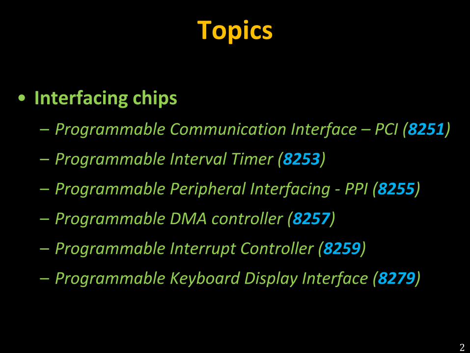
Topics
• Interfacing chips
– Programmable Communication Interface – PCI (8251)
– Programmable Interval Timer (8253)
– Programmable Peripheral Interfacing - PPI (8255)
– Programmable DMA controller (8257)
– Programmable Interrupt Controller (8259)
– Programmable Keyboard Display Interface (8279)
2
Universal Synchronous Asynchronous Receiver
Transmitter
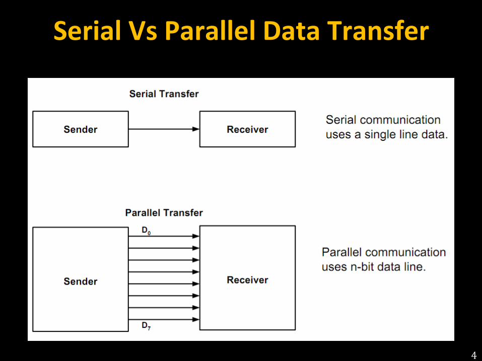
Serial Vs Parallel Data Transfer
4
Synchronous Vs Asynchronous
• Asynchronous transfer does not require clock
signal.
• However, it transfers extra bits(start bits and stop
bits) during data communication.
• Synchronous does not transfer extra bits.
However, it requires clock signal.
5
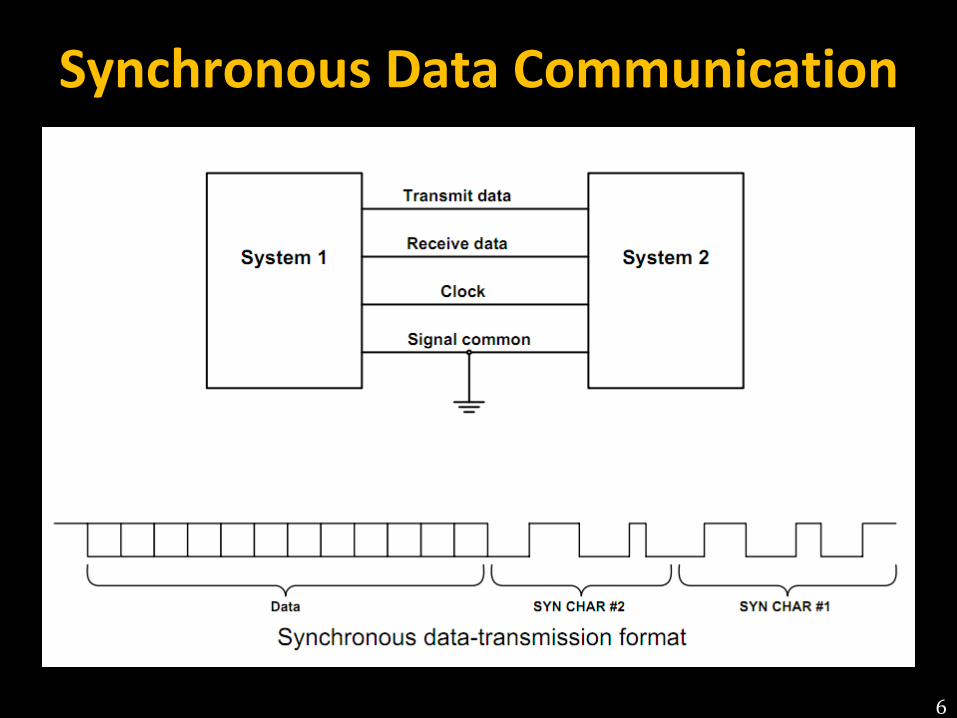
Synchronous Data Communication
6
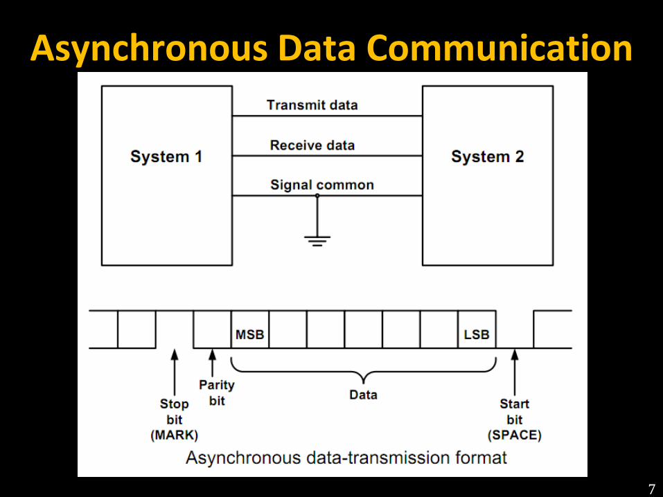
Asynchronous Data Communication
7
8251 USART
• The 8251 USART (Universal Synchronous Asynchronous
Receiver Transmitter) is capable of implementing either
an asynchronous or synchronous serial data
communication.
• As a peripheral device of a microcomputer system, the
8251 receives parallel data from the CPU and transmits
serial data after conversion.
• This device also receives serial data from the outside and
transmits parallel data to the CPU after conversion.
8
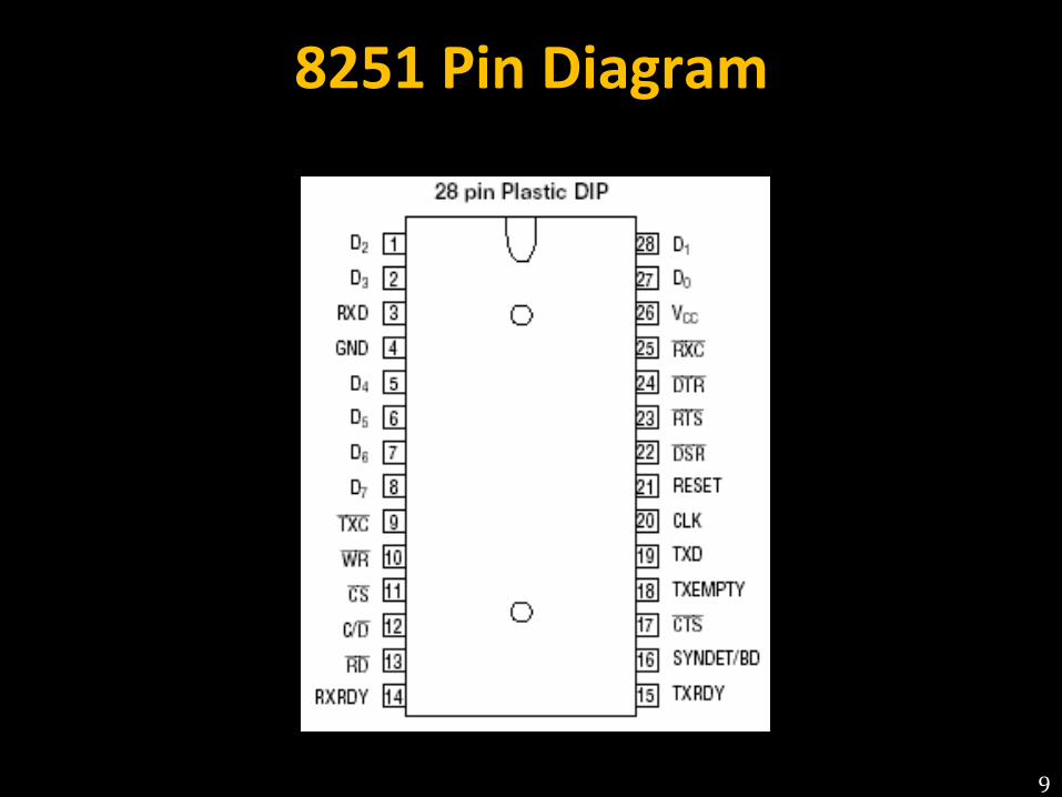
8251 Pin Diagram
9
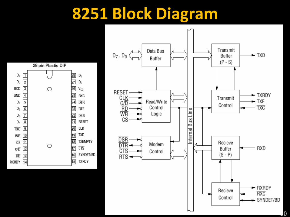
8251 Block Diagram
10
Pin Description
• D0 - D7 - This is bidirectional data bus which receive control words
and transmits data from the CPU and sends status words and
received data to CPU.
• RESET - A "High" on this input forces the 8251 into "reset status .
The min. reset width is six clock inputs during the operating status
of CLK.
• CLK - CLK signal is used to generate internal device timing. CLK
signal is independent of RXC or TXC.
• WR - This is the "active low" input terminal which receives a signal
for writing transmit data and control words from the CPU into the
8251.
11
Pin Description
• RD - This is the "active low" input terminal which receives a signal
for reading receive data and status words from the 8251.
• C/D - This is an input terminal which receives a signal for selecting
data or command words and status words when the 8251 is
accessed by the CPU.
• CS - This is the "active low" input terminal which selects the 8251 at
low level when the CPU accesses.
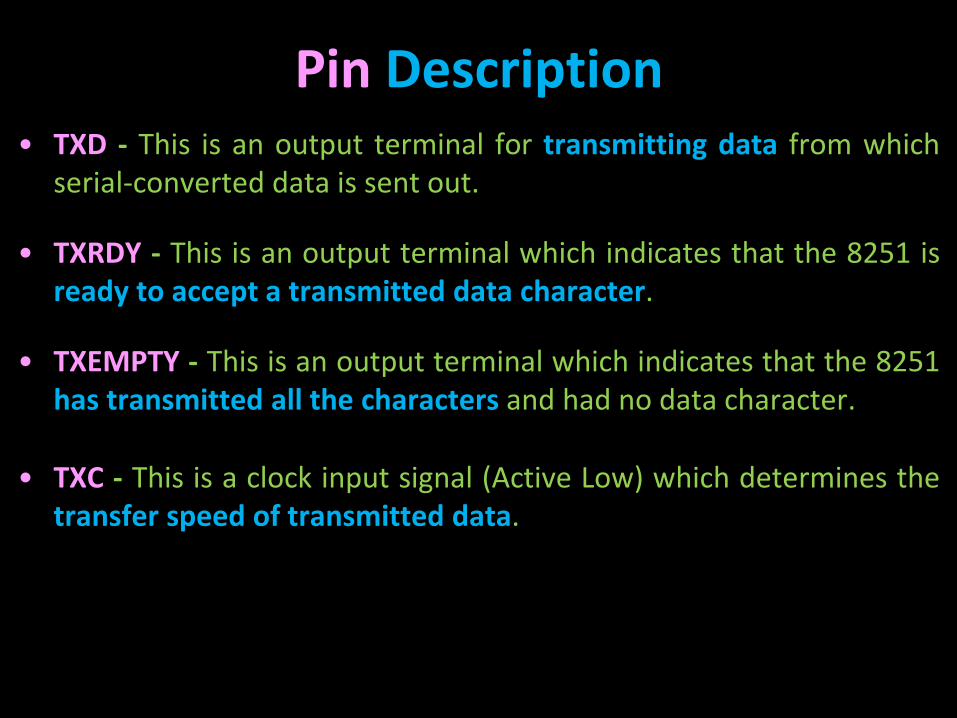
Pin Description
• TXD - This is an output terminal for transmitting data from which
serial-converted data is sent out.
• TXRDY - This is an output terminal which indicates that the 8251 is
ready to accept a transmitted data character.
• TXEMPTY - This is an output terminal which indicates that the 8251
has transmitted all the characters and had no data character.
• TXC - This is a clock input signal (Active Low) which determines the
transfer speed of transmitted data.
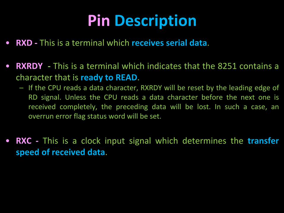
Pin Description
• RXD - This is a terminal which receives serial data.
• RXRDY - This is a terminal which indicates that the 8251 contains a
character that is ready to READ. – If the CPU reads a data character, RXRDY will be reset by the leading edge of
RD signal. Unless the CPU reads a data character before the next one is
received completely, the preceding data will be lost. In such a case, an
overrun error flag status word will be set.
• RXC - This is a clock input signal which determines the transfer
speed of received data.
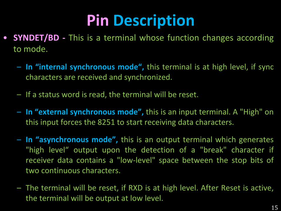
Pin Description • SYNDET/BD - This is a terminal whose function changes according
to mode.
– In i ter al synchronous ode , this terminal is at high level, if sync
characters are received and synchronized.
– If a status word is read, the terminal will be reset.
– In e ter al synchronous ode , this is an input terminal. A "High" on
this input forces the 8251 to start receiving data characters.
– In as chro ous ode , this is an output terminal which generates
"high level“ output upon the detection of a "break" character if
receiver data contains a "low-level" space between the stop bits of
two continuous characters.
– The terminal will be reset, if RXD is at high level. After Reset is active,
the terminal will be output at low level. 15
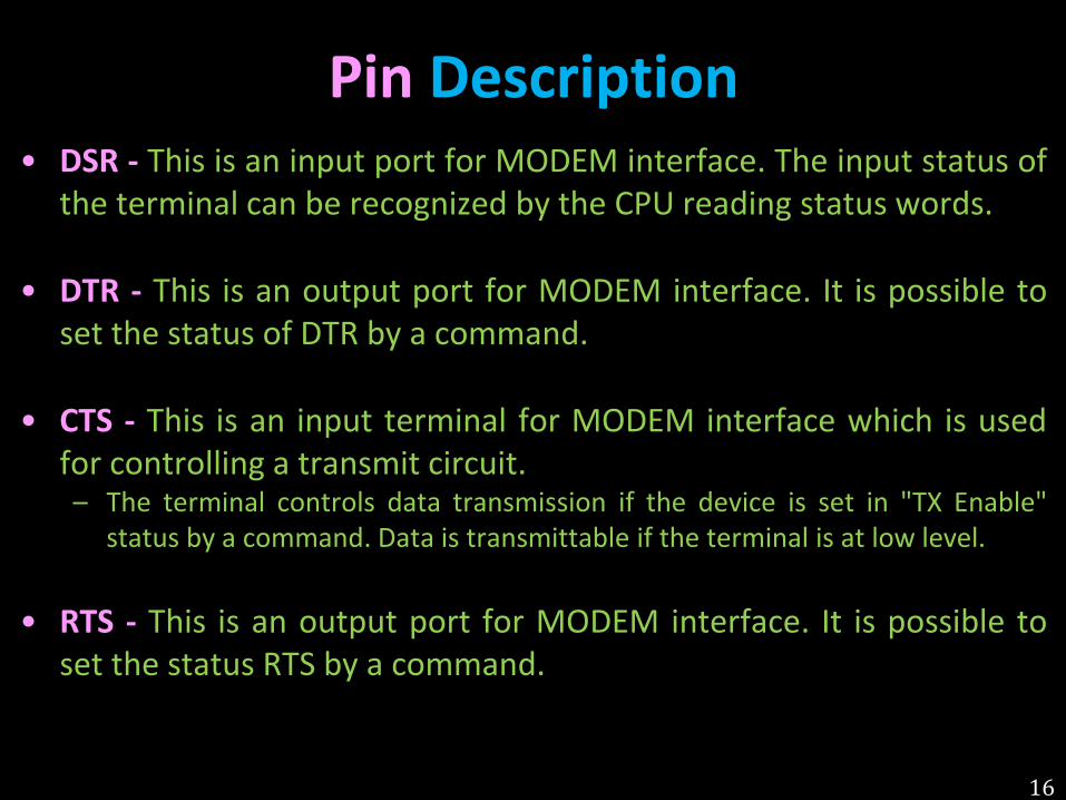
Pin Description
• DSR - This is an input port for MODEM interface. The input status of
the terminal can be recognized by the CPU reading status words.
• DTR - This is an output port for MODEM interface. It is possible to
set the status of DTR by a command.
• CTS - This is an input terminal for MODEM interface which is used
for controlling a transmit circuit. – The terminal controls data transmission if the device is set in "TX Enable"
status by a command. Data is transmittable if the terminal is at low level.
• RTS - This is an output port for MODEM interface. It is possible to
set the status RTS by a command.
16
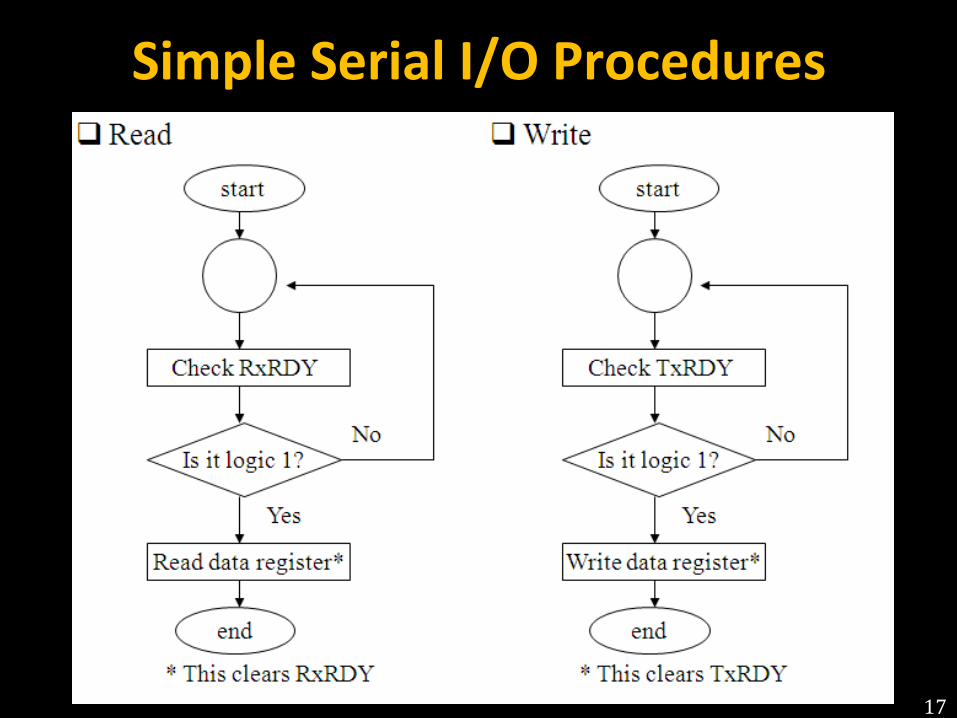
Simple Serial I/O Procedures
17
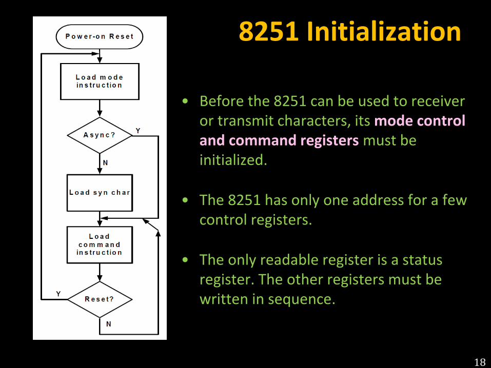
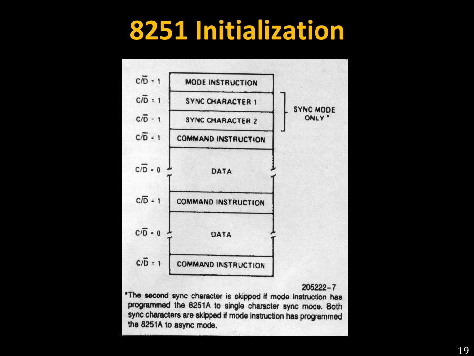
8251 Initialization
• Before the 8251 can be used to receiver
or transmit characters, its mode control
and command registers must be
initialized.
• The 8251 has only one address for a few
control registers.
• The only readable register is a status
register. The other registers must be
written in sequence.
18
8251 Initialization
19
8251 Control Words
• There are two types of control word.
1. Mode instruction (setting of function)
2. Command (setting of operation)
• Apart from the control words, a Status Word is
present in 8251 to see the internal status.
20
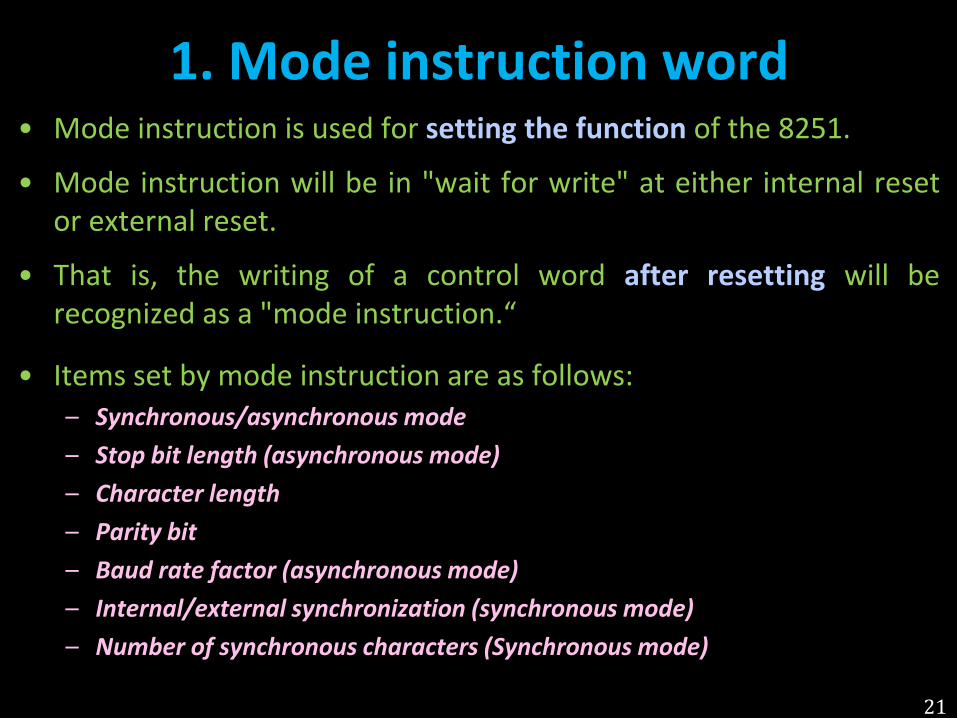
1. Mode instruction word • Mode instruction is used for setting the function of the 8251.
• Mode instruction will be in "wait for write" at either internal reset
or external reset.
• That is, the writing of a control word after resetting will be
recognized as a "mode instruction.“
• Items set by mode instruction are as follows:
– Synchronous/asynchronous mode
– Stop bit length (asynchronous mode)
– Character length
– Parity bit
– Baud rate factor (asynchronous mode)
– Internal/external synchronization (synchronous mode)
– Number of synchronous characters (Synchronous mode)
21
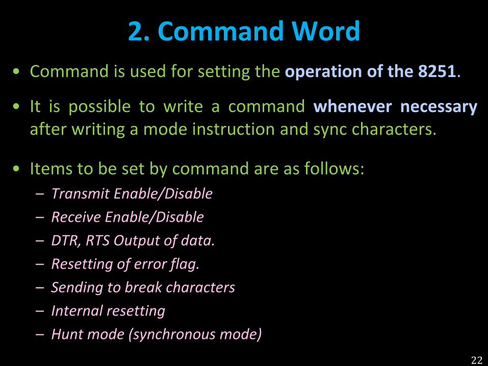
2. Command Word
• Command is used for setting the operation of the 8251.
• It is possible to write a command whenever necessary
after writing a mode instruction and sync characters.
• Items to be set by command are as follows:
– Transmit Enable/Disable
– Receive Enable/Disable
– DTR, RTS Output of data.
– Resetting of error flag.
– Sending to break characters
– Internal resetting
– Hunt mode (synchronous mode)
22
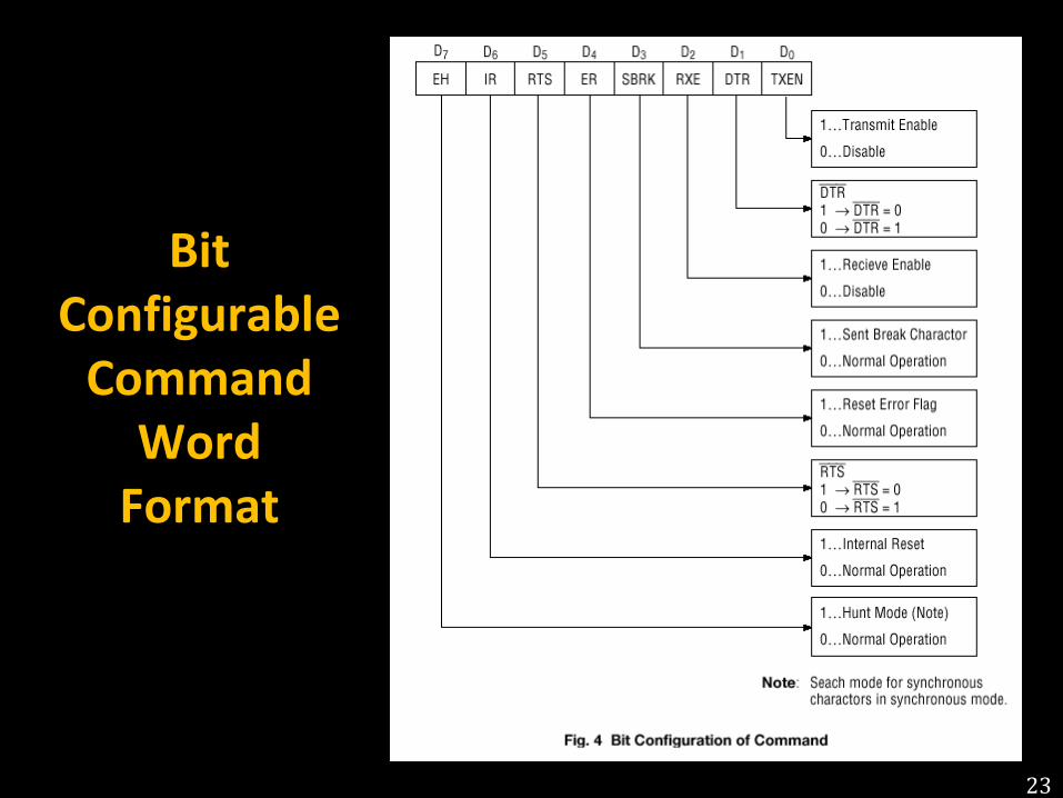
Bit
Configurable
Command
Word
Format
23
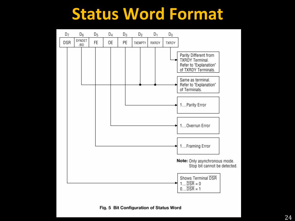
Status Word Format
24
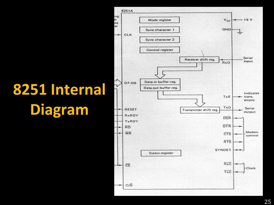
8251 Internal
Diagram
25
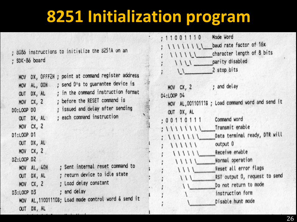
8251 Initialization program
26
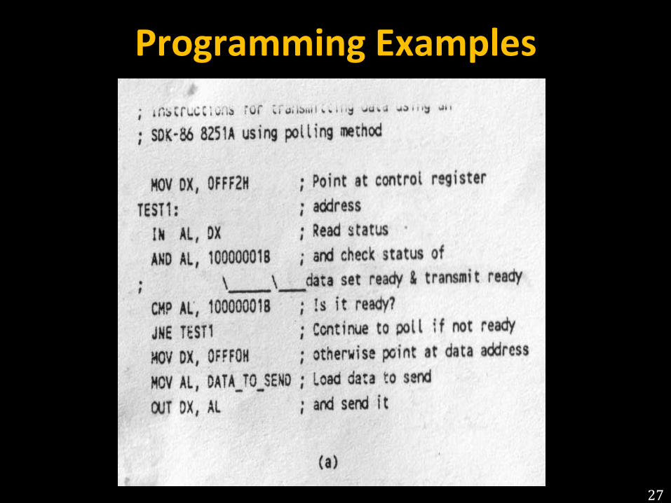
Programming Examples
27
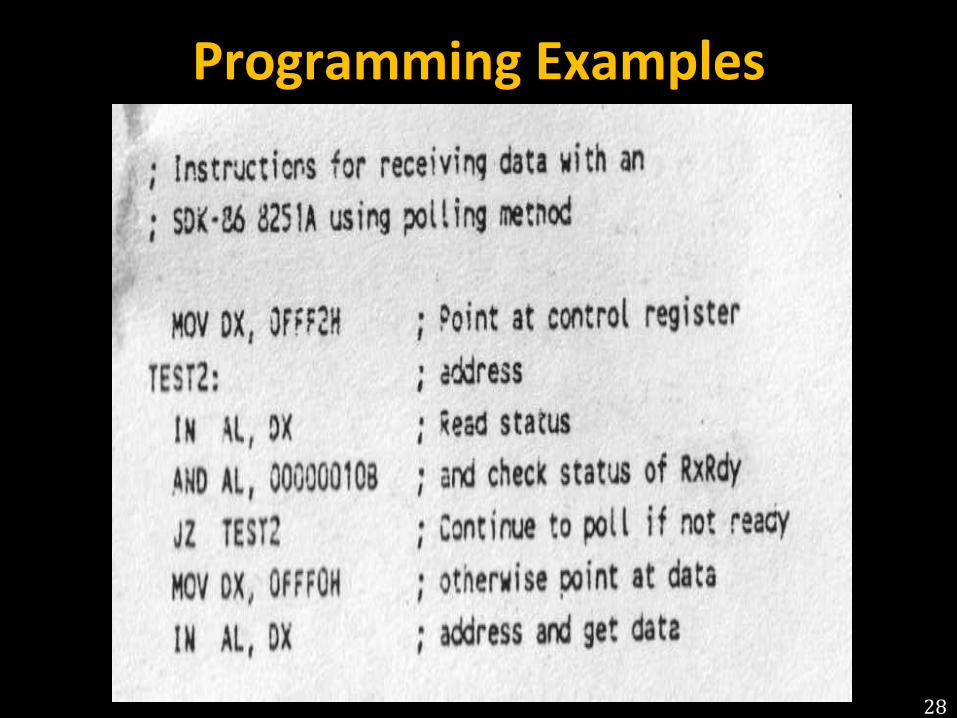
Programming Examples
28

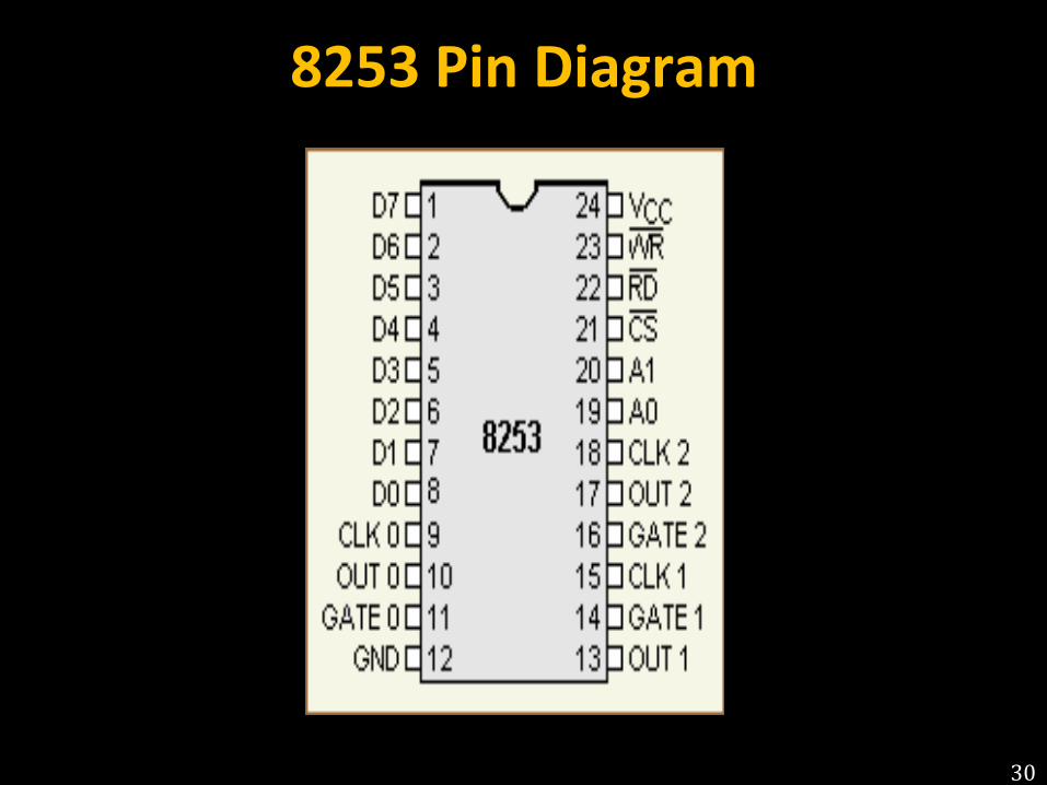
8253 Pin Diagram
30
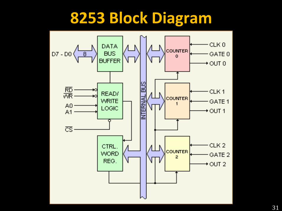
8253 Block Diagram
31
Pin Description
• Clock: This is the clock input for the counter. The counter
is 16 bits. – The maximum clock frequency is 1 / 380 nanoseconds or
2.6 megahertz. The minimum clock frequency is DC or
static operation.
• Out: This single output line is the signal that is the final
programmed output of the device. – Actual operation of the out line depends on how the
device has been programmed.
• Gate: This input can act as a gate for the clock input
line, or it can act as a start pulse, depending on the
programmed mode of the counter.
32
Counter Features
• Each counter is identical, and each consists of a 16-bit,
pre-settable, down counter.
• Each is fully independent and can be easily read by the
CPU.
• When the counter is read, the data within the counter
will not be disturbed.
• This allows the system or your own program to monitor
the counter's value at any time, without disrupting the
overall function of the 8253.
33
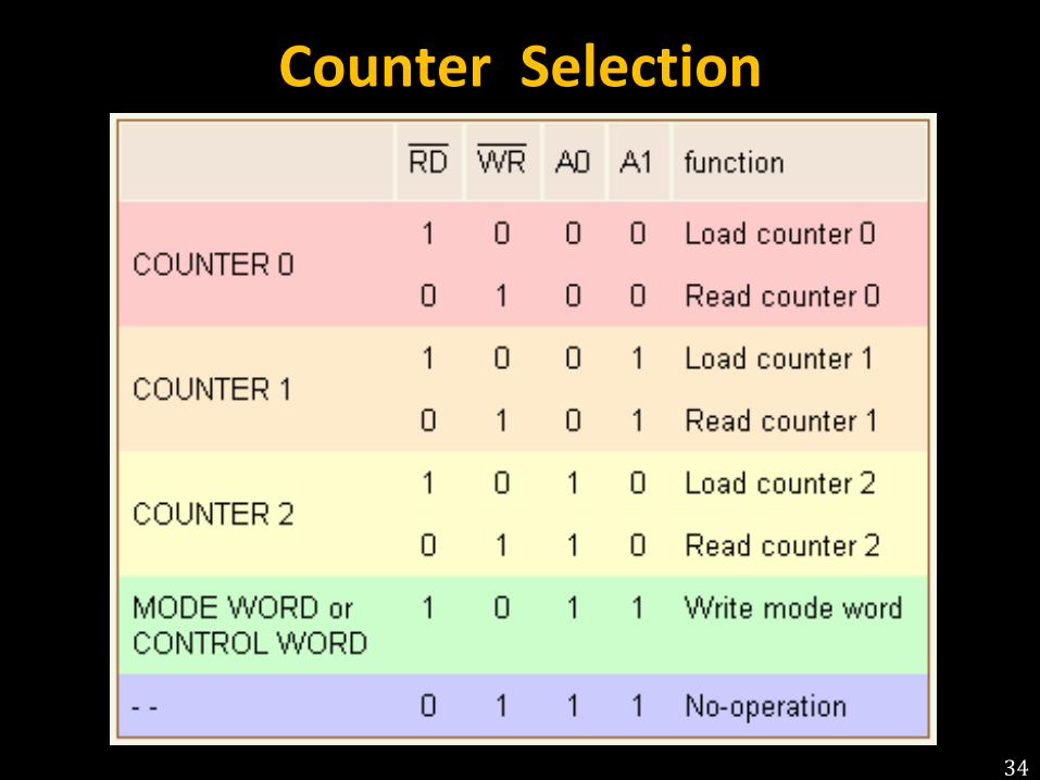
Counter Selection
34
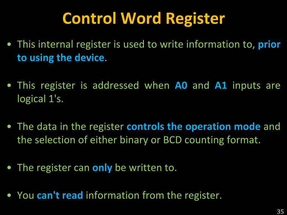
Control Word Register
• This internal register is used to write information to, prior
to using the device.
• This register is addressed when A0 and A1 inputs are
logical 1's.
• The data in the register controls the operation mode and
the selection of either binary or BCD counting format.
• The register can only be written to.
• You can't read information from the register.
35
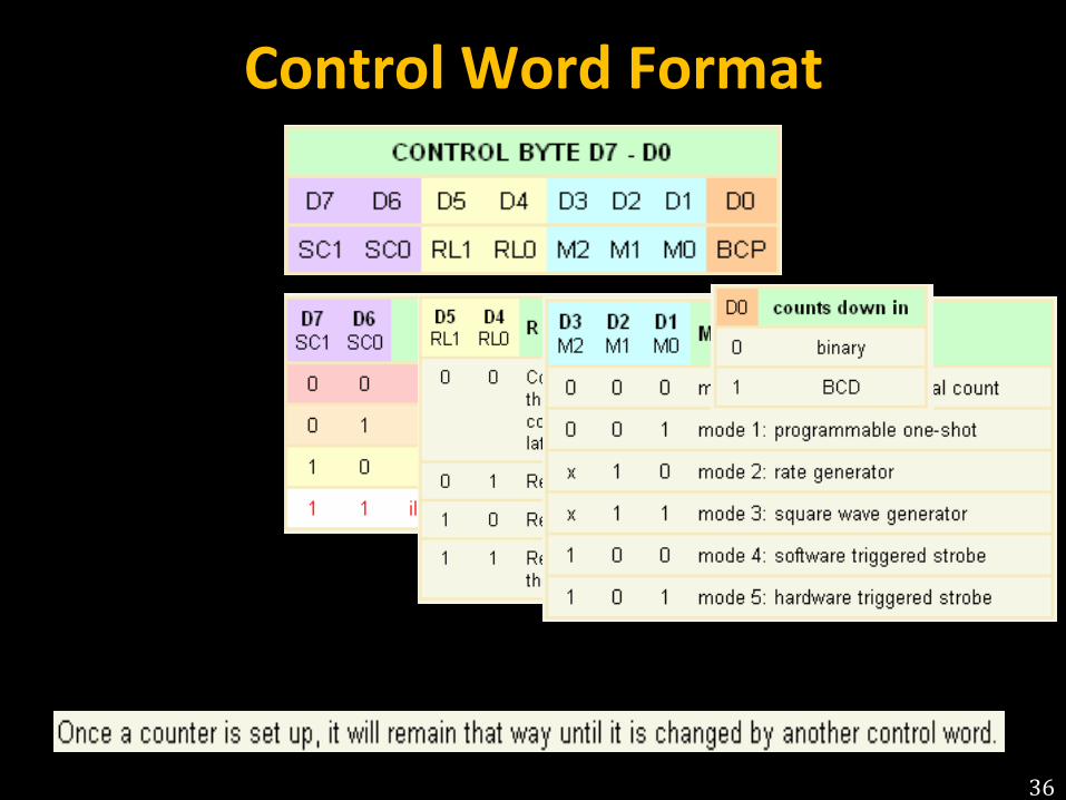
Control Word Format
36
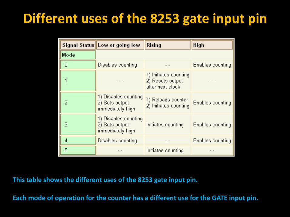
This table shows the different uses of the 8253 gate input pin.
Each mode of operation for the counter has a different use for the GATE input pin.
Different uses of the 8253 gate input pin
Timer Modes - Mode 0
• Interrupt on Terminal Count
• The counter will be programmed to an initial value and afterwards
counts down at a rate equal to the input clock frequency(8 MHz).
• When the count is equal to 0, the OUT pin will be a logical 1.
• The output will stay a logical 1 until the counter is reloaded with a
new value or the same value or until a mode word is written to the
device.
• Once the counter starts counting down, the GATE input can disable
the internal counting by setting the GATE to a logical 0.
38
Timer Modes - Mode 1
• Programmable One-Shot
• In mode 1, the device can be setup to give an output
pulse that is an integer number of clock pulses.
• The one-shot is triggered on the rising edge of the GATE
input.
• If the trigger occurs during the pulse output, the 8253 will
be retriggered again.
39
Timer Modes - Mode 2
• Rate Generator
• The counter that is programmed for mode 2 becomes a
"divide by n" counter.
• The OUT pin of the counter goes to low for one input
clock period.
• The time between the pulses of going low is dependent
on the present count in the counter's register.
40
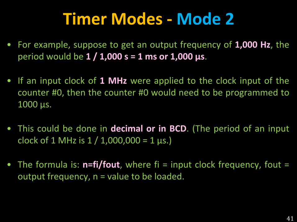
Timer Modes - Mode 2
• For example, suppose to get an output frequency of 1,000 Hz, the
period would be 1 / 1,000 s = 1 ms or 1,000 µs.
• If an input clock of 1 MHz were applied to the clock input of the
counter #0, then the counter #0 would need to be programmed to
1000 µs.
• This could be done in decimal or in BCD. (The period of an input
clock of 1 MHz is 1 / 1,000,000 = 1 µs.)
• The formula is: n=fi/fout, where fi = input clock frequency, fout =
output frequency, n = value to be loaded.
41
Timer Modes - Mode 3
• Square Wave Generator
• Mode 3 is similar to the mode 2 except that the
output will be high for half the period and low for
half.
• If the count is odd, the output will be high for
(n+1)/2 and low for (n-1)/2 counts.
42
Timer Modes - Mode 4
• Software Triggered Strobe
• In this mode the programmer can set up the counter
to give an output timeout starting when the register
is loaded.
• On the terminal count, when the counter equals to 0,
the output will go to a logical 0 for one clock period
and then returns to a logical 1.
• Firstly, when the mode is set, the output will be a
logical 1.
43
Timer Modes - Mode 5
• Hardware Triggered Strobe
• In this mode the rising edge of the trigger input will start the
counting of the counter.
• The output goes low for one clock at the terminal count.
• The counter is retriggerable, thus meaning that if the trigger input
is taken low and then high during a count sequence, the sequence
will start over.
• When the external trigger input goes to a logical 1, the timer will
start to time out.
• If the external trigger occurs again, prior to the time completing a
full timeout, the timer will retrigger.
44

45
Introduction
• PPI – Programmable Peripheral Interface
• It is an I/O port chip used for interfacing I/O
devices with microprocessor
• Very commonly used peripheral chip
• Knowledge of 8255 essential for students in the
Microprocessors lab for Interfacing experiments
46
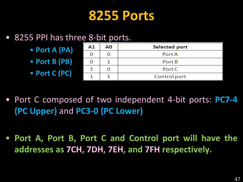
8255 Ports
• 8255 PPI has three 8-bit ports.
• Port A (PA)
• Port B (PB)
• Port C (PC)
• Port C composed of two independent 4-bit ports: PC7-4
(PC Upper) and PC3-0 (PC Lower)
• Port A, Port B, Port C and Control port will have the
addresses as 7CH, 7DH, 7EH, and 7FH respectively.
47
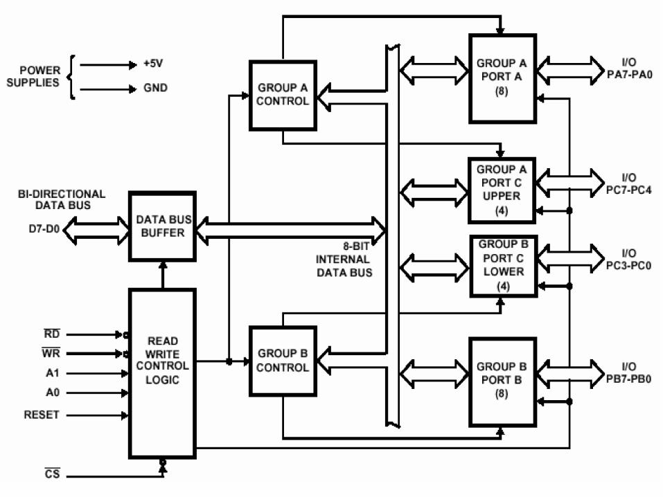
Block Diagram
48
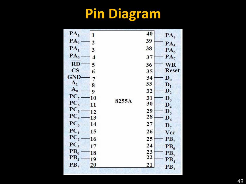
Pin Diagram
49
Pin Description
• PA7-PA0 : These are eight port A lines that acts as either latched
output or buffered input lines depending upon the
control word loaded into the control word register.
• PC7-PC4 : Upper nibble of port C lines. They may act as either
output latches or input buffers lines.
• PC3-PC0 : These are the lower port C lines, other details are the
same as PC7-PC4 lines.
• PB0-PB7 : These are the eight port B lines which are used as
latched output lines or buffered input lines in the same
way as port A.
50
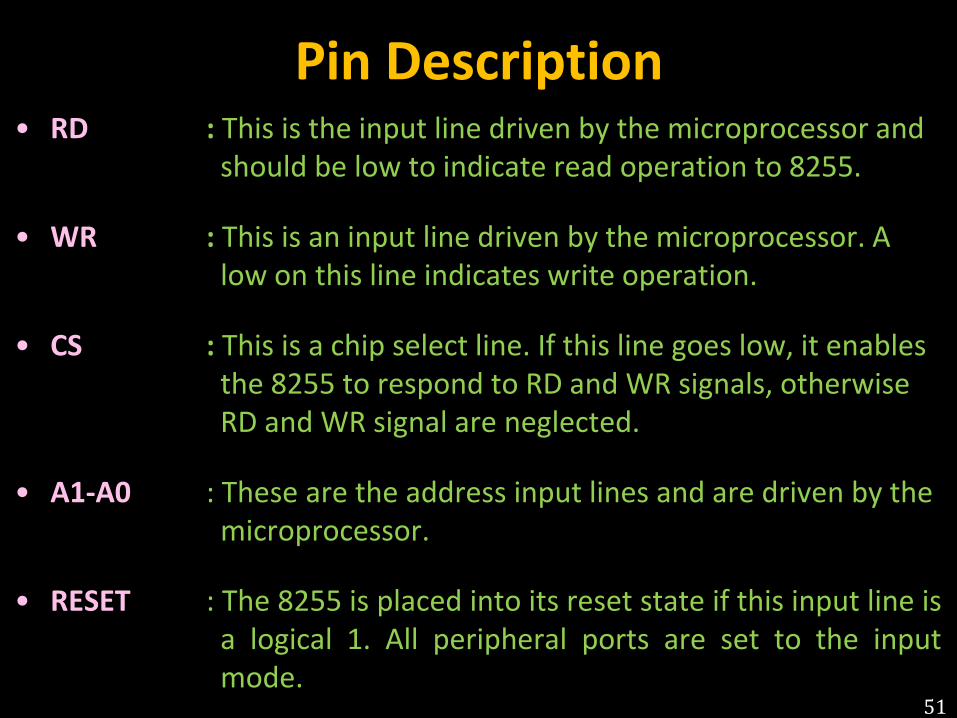
Pin Description • RD : This is the input line driven by the microprocessor and
should be low to indicate read operation to 8255.
• WR : This is an input line driven by the microprocessor. A
low on this line indicates write operation.
• CS : This is a chip select line. If this line goes low, it enables
the 8255 to respond to RD and WR signals, otherwise
RD and WR signal are neglected.
• A1-A0 : These are the address input lines and are driven by the
microprocessor.
• RESET : The 8255 is placed into its reset state if this input line is
a logical 1. All peripheral ports are set to the input
mode. 51
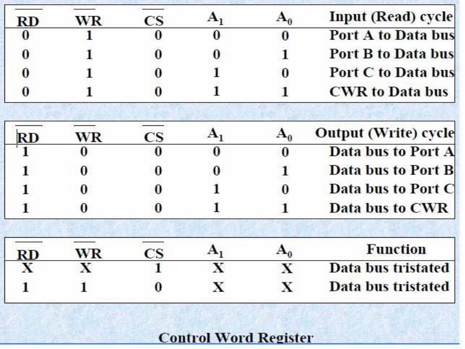
8255 Operations
• The lines A1-A0 with RD, WR and CS form the following
operations for 8255.
52
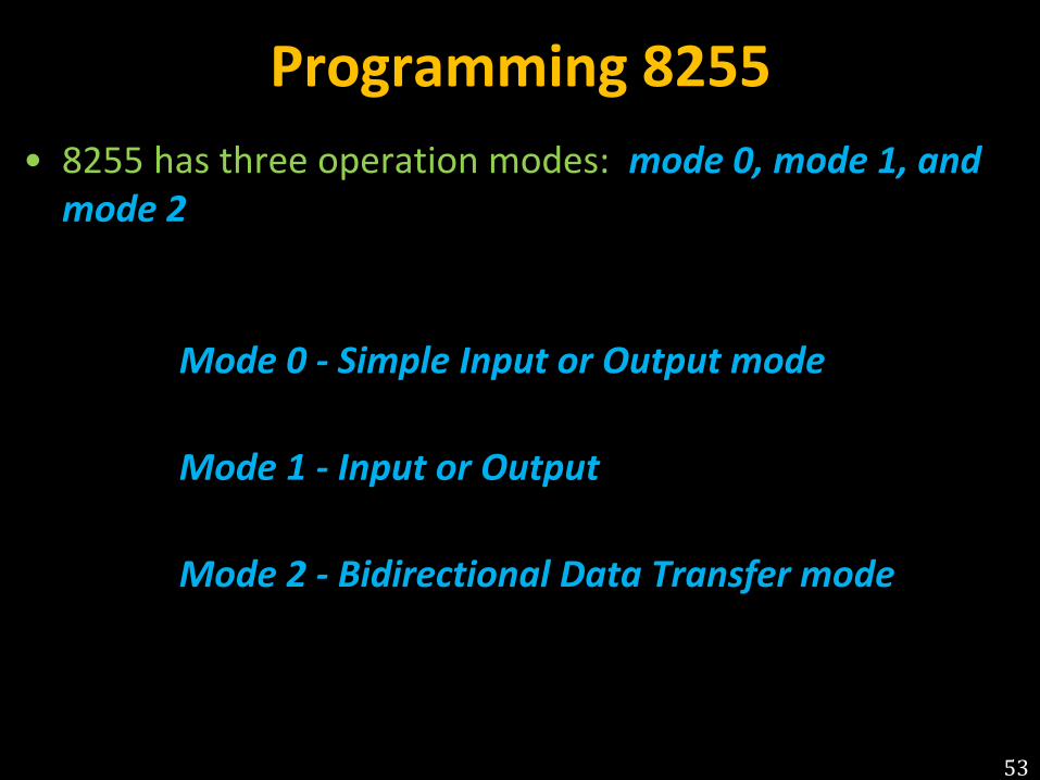
Programming 8255
• 8255 has three operation modes: mode 0, mode 1, and
mode 2
Mode 0 - Simple Input or Output mode
Mode 1 - Input or Output
Mode 2 - Bidirectional Data Transfer mode
53
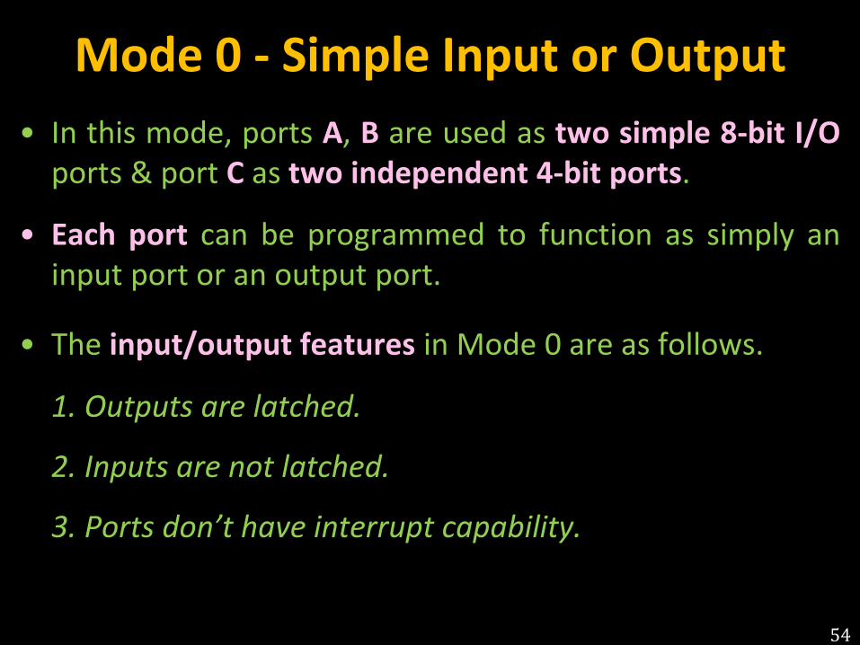
Mode 0 - Simple Input or Output
• In this mode, ports A, B are used as two simple 8-bit I/O
ports & port C as two independent 4-bit ports.
• Each port can be programmed to function as simply an
input port or an output port.
• The input/output features in Mode 0 are as follows.
1. Outputs are latched.
2. Inputs are not latched.
3. Ports don’t have interrupt apa ility.
54
Mode 1 - Input or Output with Handshake
• In this mode, handshake signals are exchanged between
the MPU and peripherals prior to data transfer.
• The features of the mode include the following:
1. Two ports (A and B) function as 8-bit I/O ports. They can be configured as either as input or output ports.
2. Each port uses three lines from port C as handshake signals. The remaining two lines of Port C can be used for simple I/O operations.
3. Input and Output data are latched.
4. Interrupt logic is supported.
55
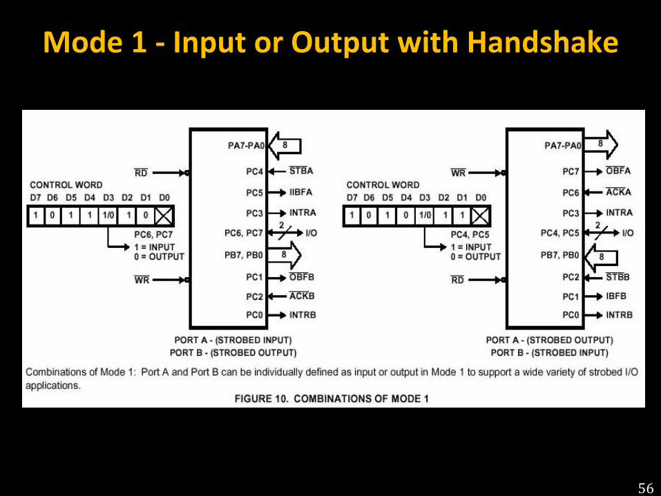
Mode 1 - Input or Output with Handshake
56
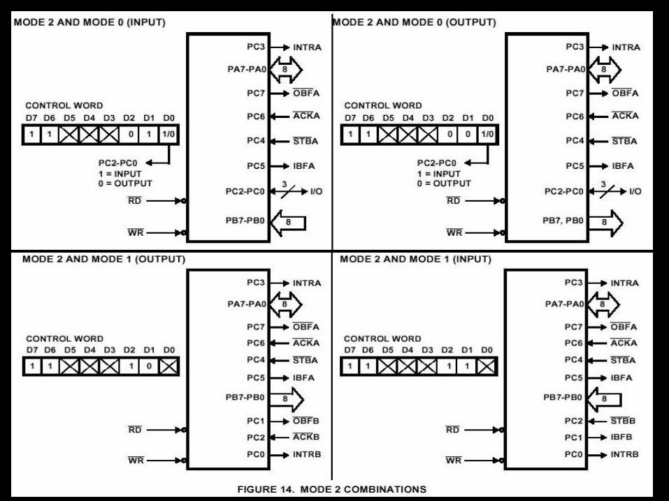
Mode 2 - Bidirectional Data Transfer
• This mode is used primarily in applications such as data
transfer between two computers.
• In this mode, Port A can be configured as the
bidirectional port, Port B either in Mode 0 or Mode 1.
• Port A uses five signals from Port C as handshake signals
for data transfer.
• The remaining three signals from Port C can be used
either as simple I/O or as handshake for port B.
57
8255 Modes Summary
• Port A can work in Mode 0, Mode 1, or Mode 2
• Port B can work in Mode 0, or Mode 1
• Port C can work in Mode 0 only, if at all
• Port A, Port B and Port C can work in Mode 0
• Port A and Port B can work in Mode 1
• Only Port A can work in Mode 2
59
8255 Control Words
• There are 2 control words in 8255.
1. Mode Definition (MD) Control word and
2. Bit Set / Reset (BSR) Control Word
• MD control word configures the ports of 8255 as
input or output in Mode 0, 1, or 2.
• PCBSR control word is used to set to 1 or reset to
0 any one selected bit of Port C
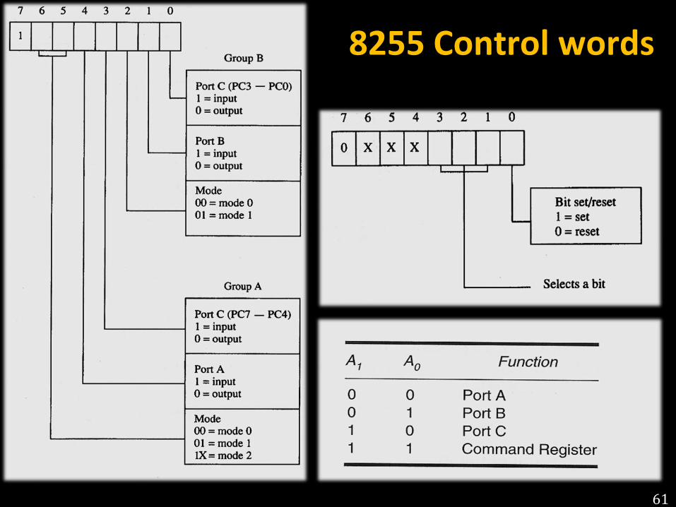
8255 Control words
61
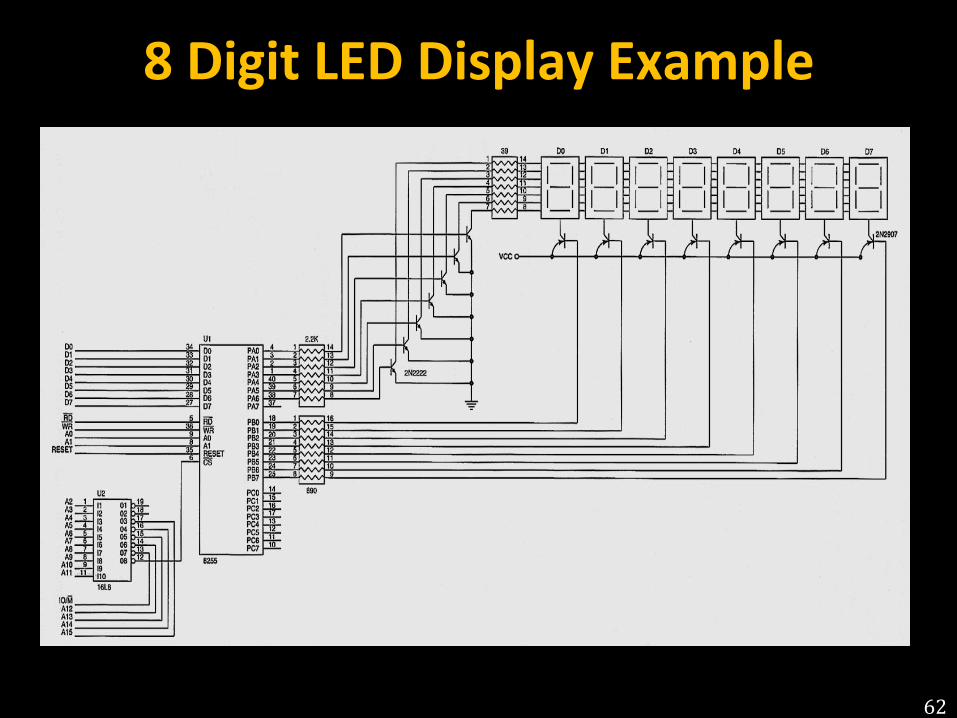
8 Digit LED Display Example
62
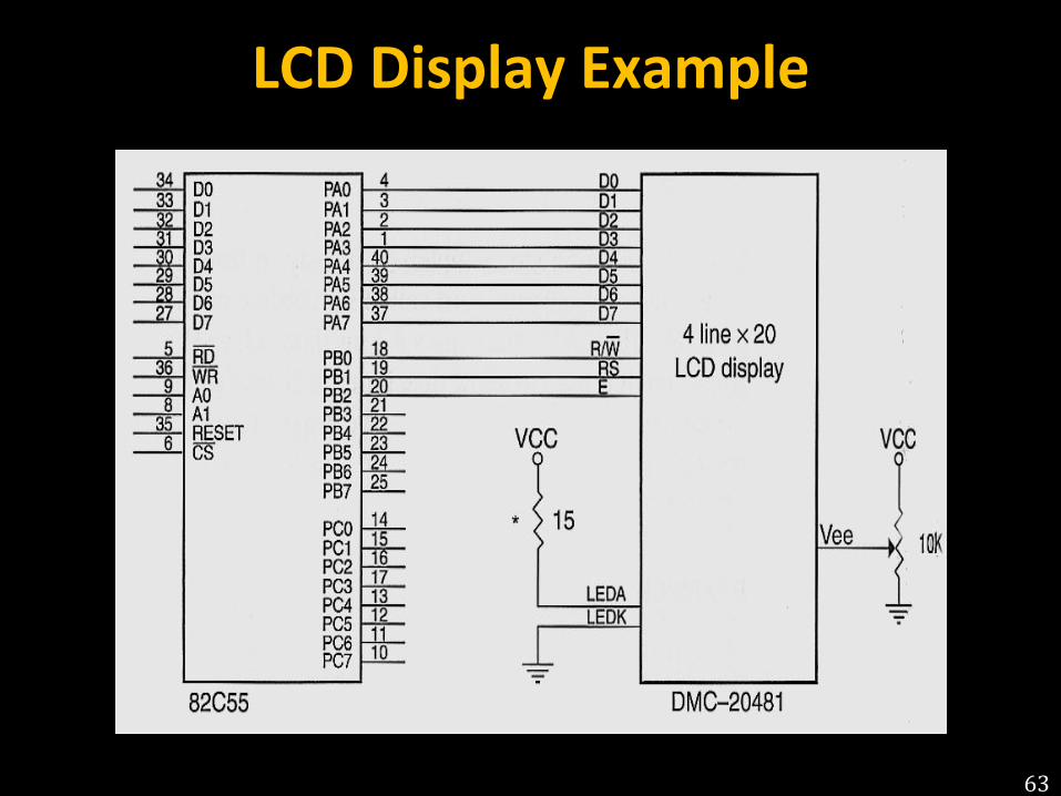
LCD Display Example
63
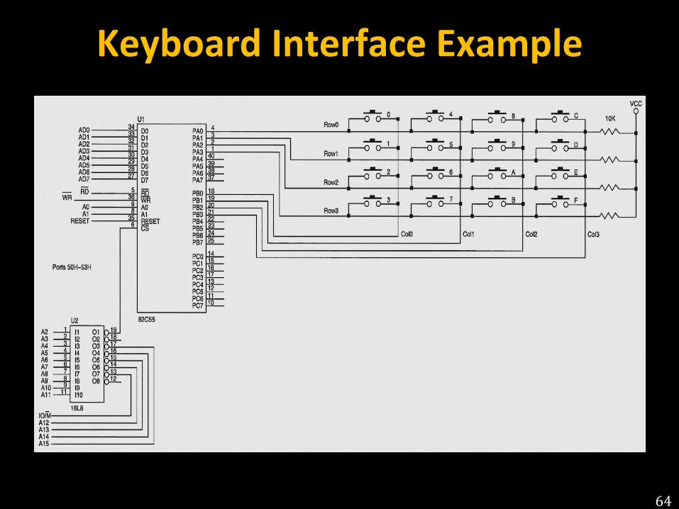
Keyboard Interface Example
64
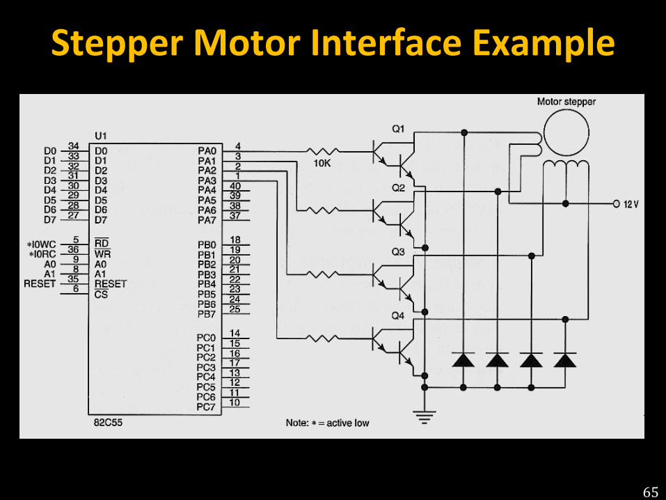
Stepper Motor Interface Example
65
66
Direct memory access
• Direct memory access (DMA) is a process in which an
external device takes over the control of system bus from
the CPU.
• DMA is for high-speed data transfer from/to mass storage
peripherals, e.g. harddisk drive, magnetic tape, CD-ROM,
and sometimes video controllers.
• The basic idea of DMA is to transfer blocks of data
directly between memory and peripherals.
• The data don’t go through the microprocessor but the
data bus is occupied.
67
Basic process of DMA – Minimum Mode
• The HOLD and HLDA pins are used to receive and acknowledge the hold request respectively.
• Normally the CPU has full control of the system bus.
• In a DMA operation, the peripheral takes over bus control temporarily.
68
Basic process of DMA – Maximum Mode
• The RQ/GT1 and RQ/GT0 pins are used to issue DMA request and receive acknowledge signals.
• Sequence of events of a typical DMA process:
1. Peripheral asserts one of the request pins, e.g. RQ/GT1 or RQ/GT0 (RQ/GT0 has higher priority)
2. 8086 completes its current bus cycle and enters into a HOLD state.
3. 8086 grants the right of bus control by asserting a grant signal via the same pin as the request signal.
4. DMA operation starts.
5. Upon completion of the DMA operation, the peripheral asserts the request/grant pin again to relinquish bus control.
69
DMA controller
• A DMA controller interfaces with several peripherals that may
request DMA.
• The controller decides the priority of simultaneous DMA
requests communicates with the peripheral and the CPU, and
provides memory addresses for data transfer.
• DMA controller commonly used with 8086 is the 8257/8237
programmable device.
• The 8257/8237 is a 4-channel device.
• Each channel is dedicated to a specific peripheral device and
capable of addressing 64 K bytes section of memory.
70
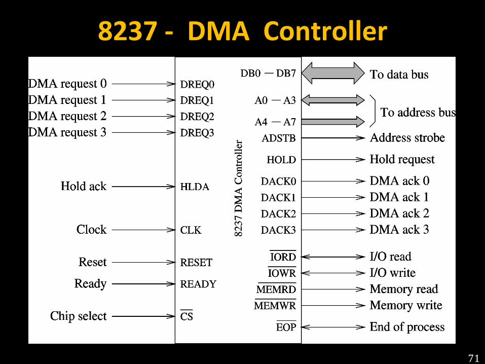
8237 - DMA Controller
71
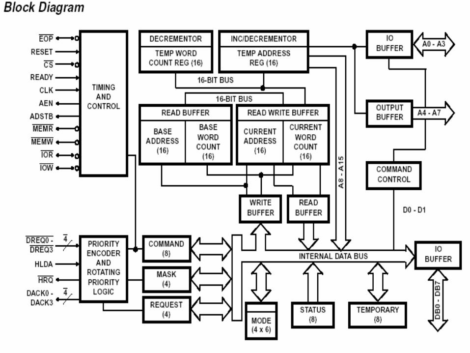
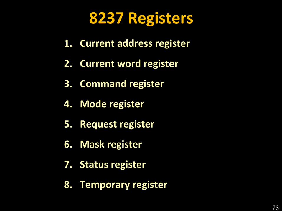
8237 Registers
1. Current address register
2. Current word register
3. Command register
4. Mode register
5. Request register
6. Mask register
7. Status register
8. Temporary register
73
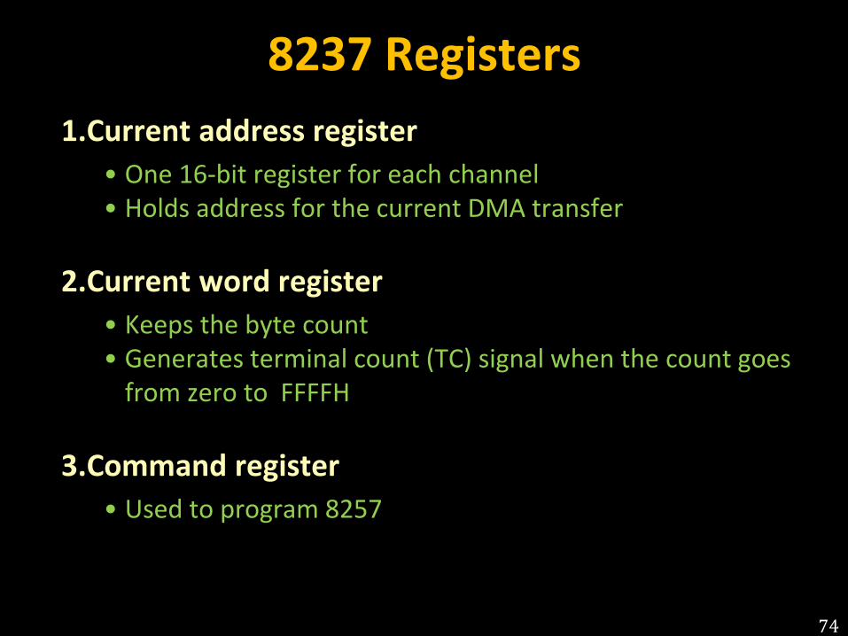
8237 Registers
1.Current address register
• One 16-bit register for each channel
• Holds address for the current DMA transfer
2.Current word register
• Keeps the byte count
• Generates terminal count (TC) signal when the count goes
from zero to FFFFH
3.Command register
• Used to program 8257
74
8237 Registers
4.Mode register
• Each channel can be programmed to
– Read or write
– Autoincrement or autodecrement the address
– Autoinitialize the channel
5.Request register • For software-initiated DMA
6.Mask register • Used to disable a specific channel
7.Status register
8.Temporary register
• Used for memory-to-memory transfers
75
Types of data transfer
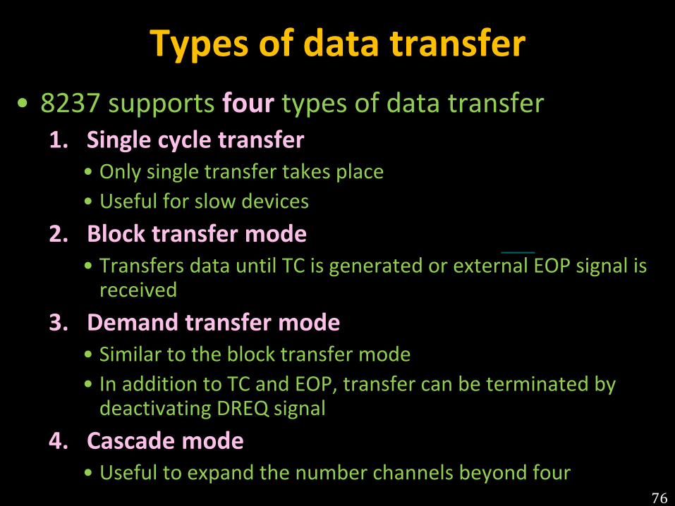
• 8237 supports four types of data transfer
1. Single cycle transfer
• Only single transfer takes place
• Useful for slow devices
2. Block transfer mode
• Transfers data until TC is generated or external EOP signal is received
3. Demand transfer mode
• Similar to the block transfer mode
• In addition to TC and EOP, transfer can be terminated by deactivating DREQ signal
4. Cascade mode
• Useful to expand the number channels beyond four 76
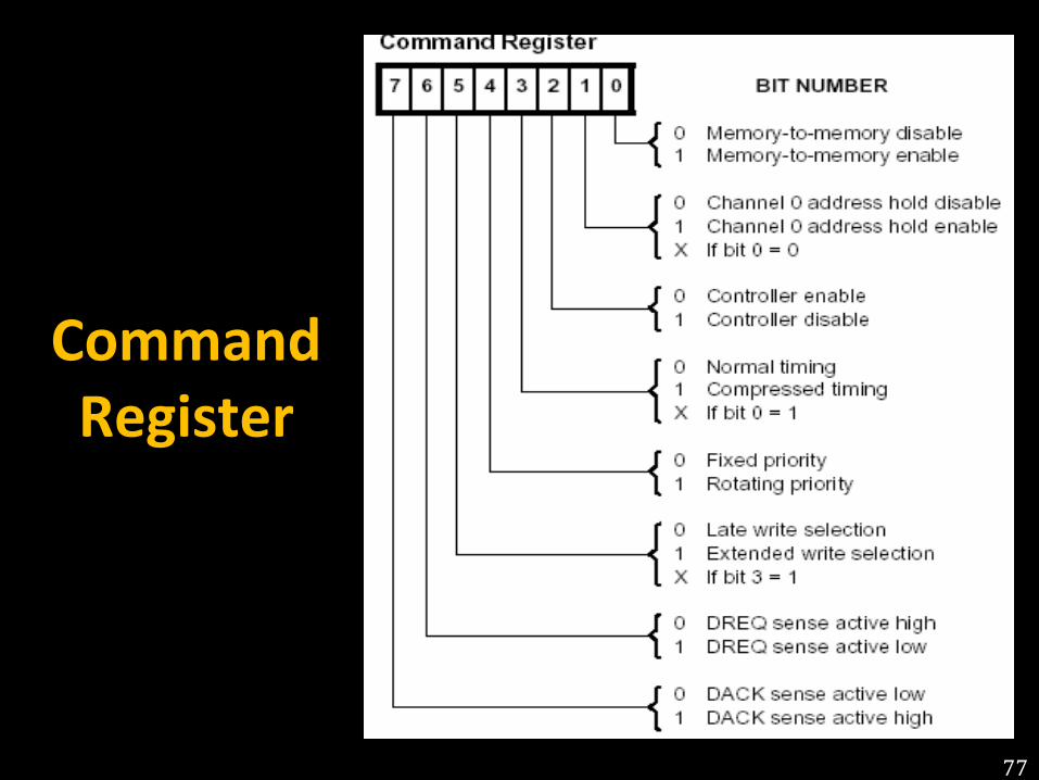
Command
Register
77
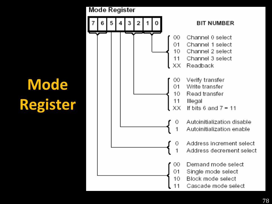
Mode
Register
78
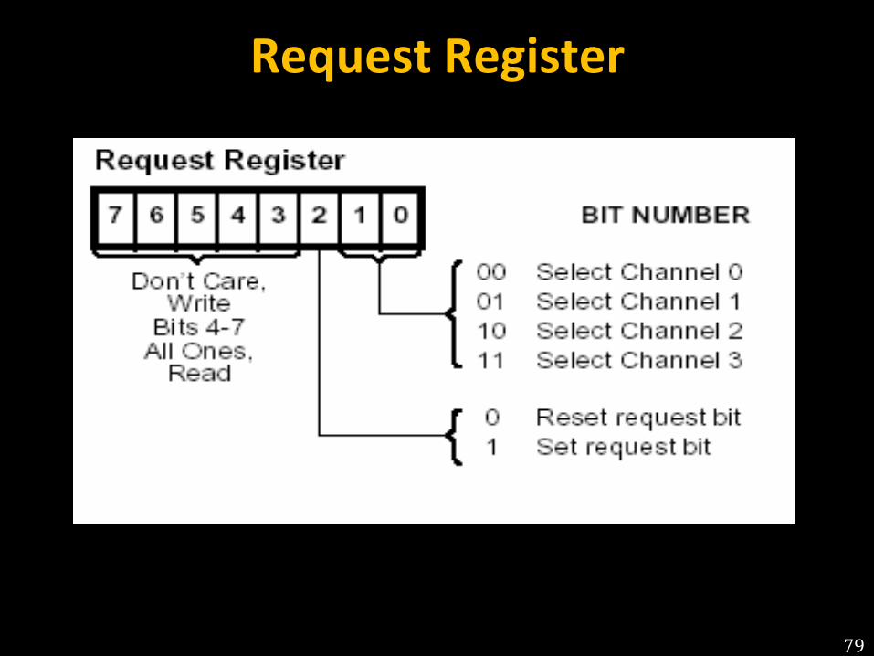
Request Register
79
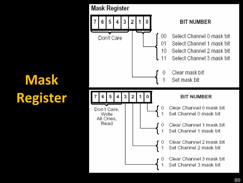
Mask
Register
80
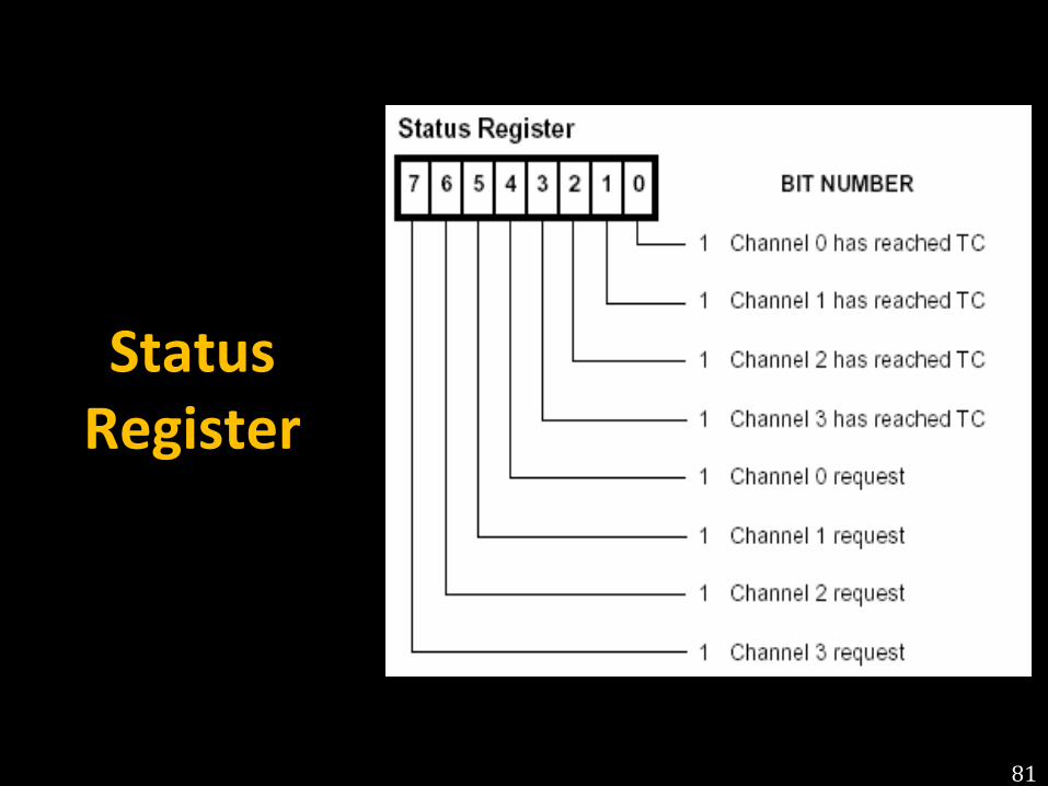
Status
Register
81
82
8259 Features
• 8259 is Programmable Interrupt Controller (PIC)
• It is a tool for managing the interrupt requests.
• 8259 is a very flexible peripheral controller chip:
– PIC can deal with up to 64 interrupt inputs
– interrupts can be masked individually.
– various priority schemes can also programmed.
83
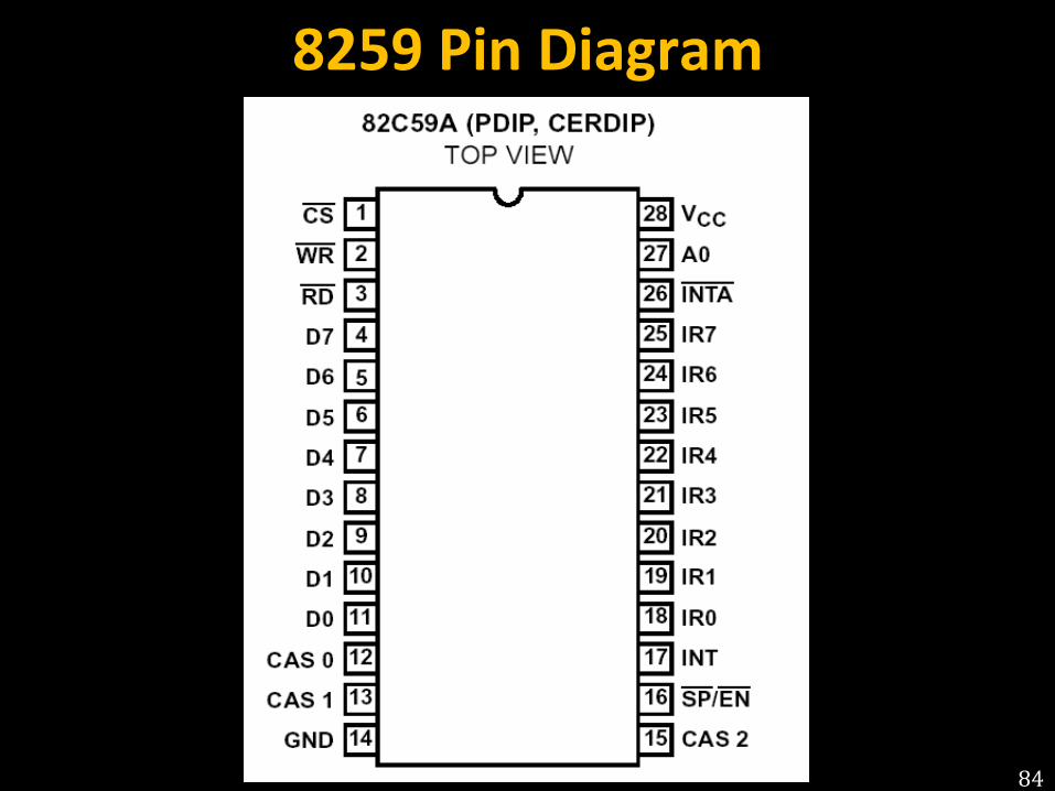
8259 Pin Diagram
84
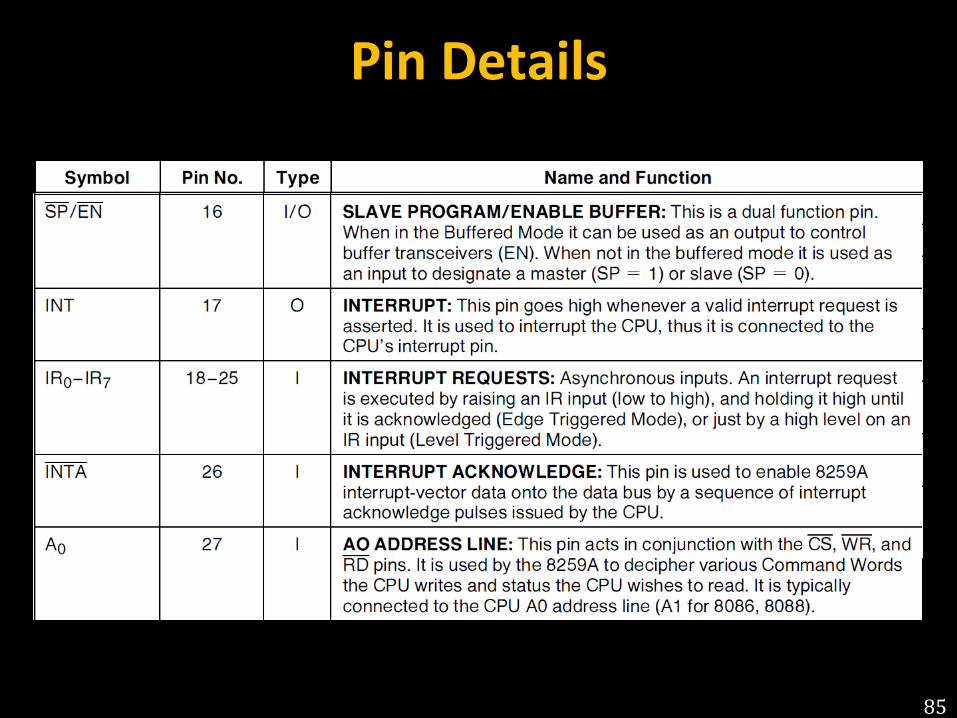
Pin Details
85
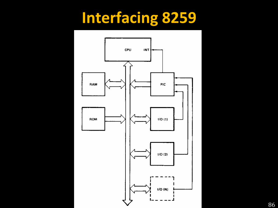
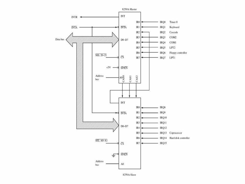
Interfacing 8259
86
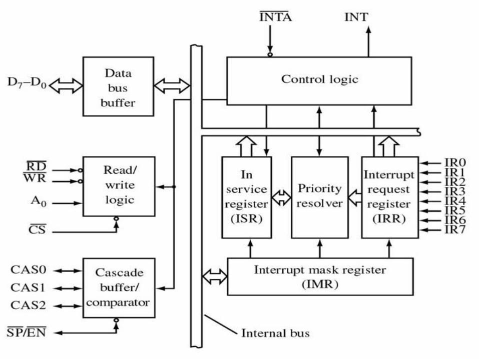
Block Diagram
87
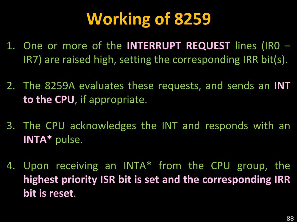
Working of 8259
1. One or more of the INTERRUPT REQUEST lines (IR0 –
IR7) are raised high, setting the corresponding IRR bit(s).
2. The 8259A evaluates these requests, and sends an INT
to the CPU, if appropriate.
3. The CPU acknowledges the INT and responds with an
INTA* pulse.
4. Upon receiving an INTA* from the CPU group, the
highest priority ISR bit is set and the corresponding IRR
bit is reset.
88
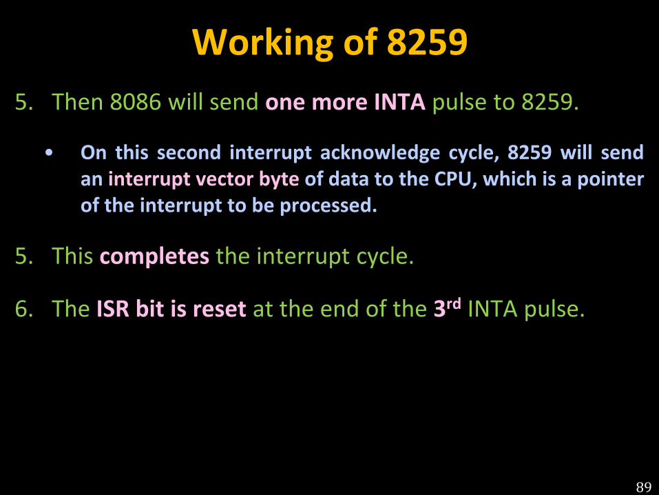
Working of 8259
5. Then 8086 will send one more INTA pulse to 8259.
• On this second interrupt acknowledge cycle, 8259 will send
an interrupt vector byte of data to the CPU, which is a pointer
of the interrupt to be processed.
5. This completes the interrupt cycle.
6. The ISR bit is reset at the end of the 3rd INTA pulse.
89
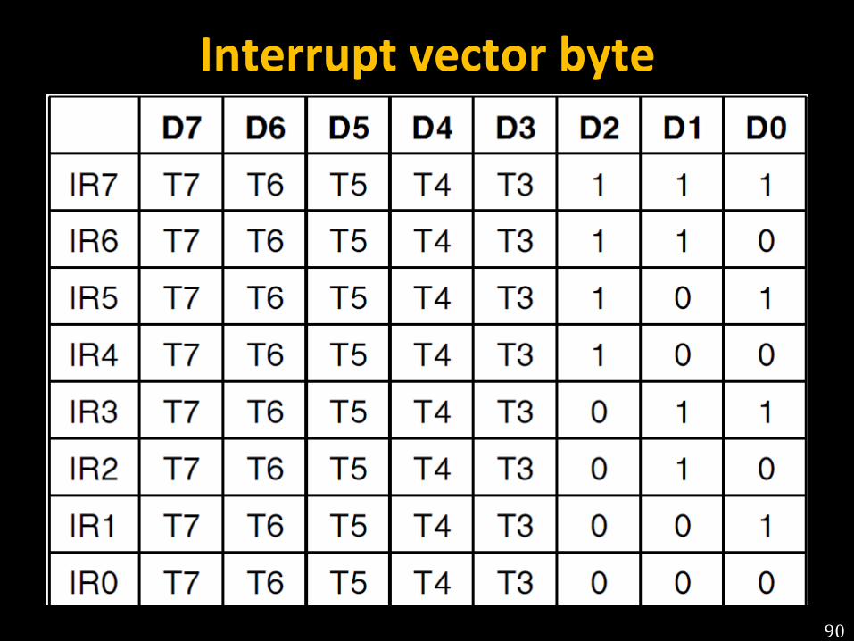
Interrupt vector byte
90
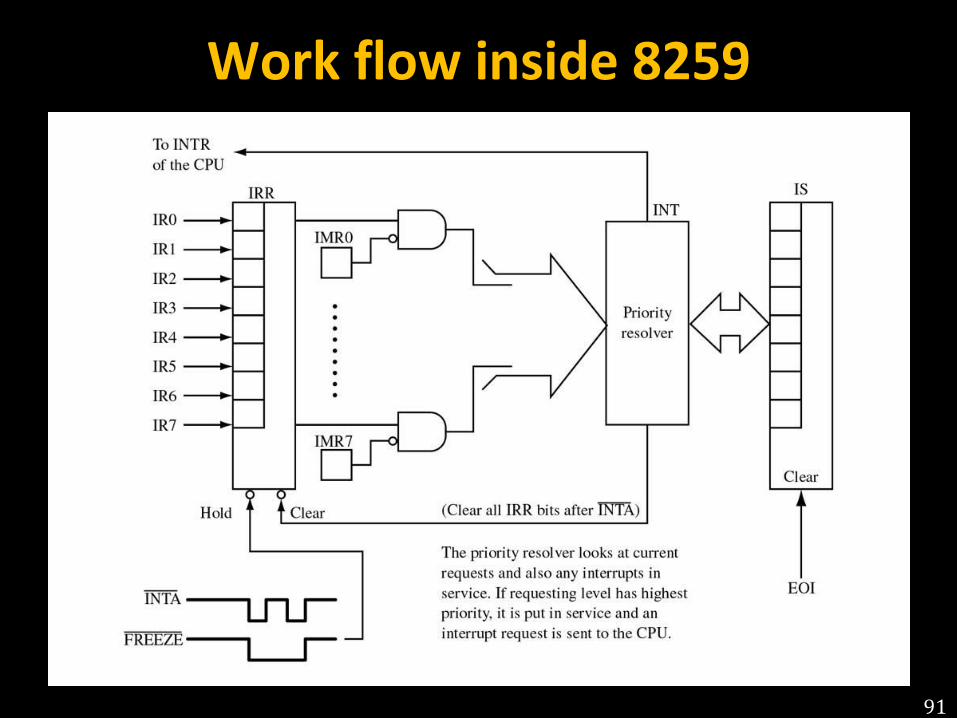
Work flow inside 8259
91
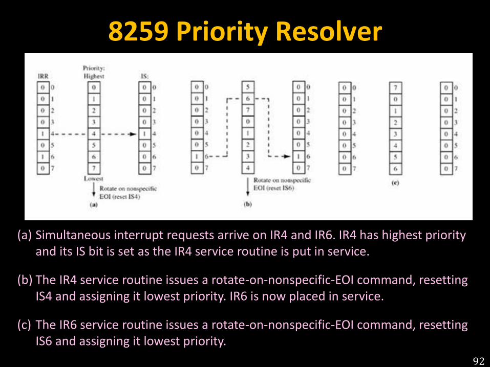
8259 Priority Resolver
92
(a) Simultaneous interrupt requests arrive on IR4 and IR6. IR4 has highest priority
and its IS bit is set as the IR4 service routine is put in service.
(b) The IR4 service routine issues a rotate-on-nonspecific-EOI command, resetting
IS4 and assigning it lowest priority. IR6 is now placed in service.
(c) The IR6 service routine issues a rotate-on-nonspecific-EOI command, resetting
IS6 and assigning it lowest priority.
Cascaded Mode
93
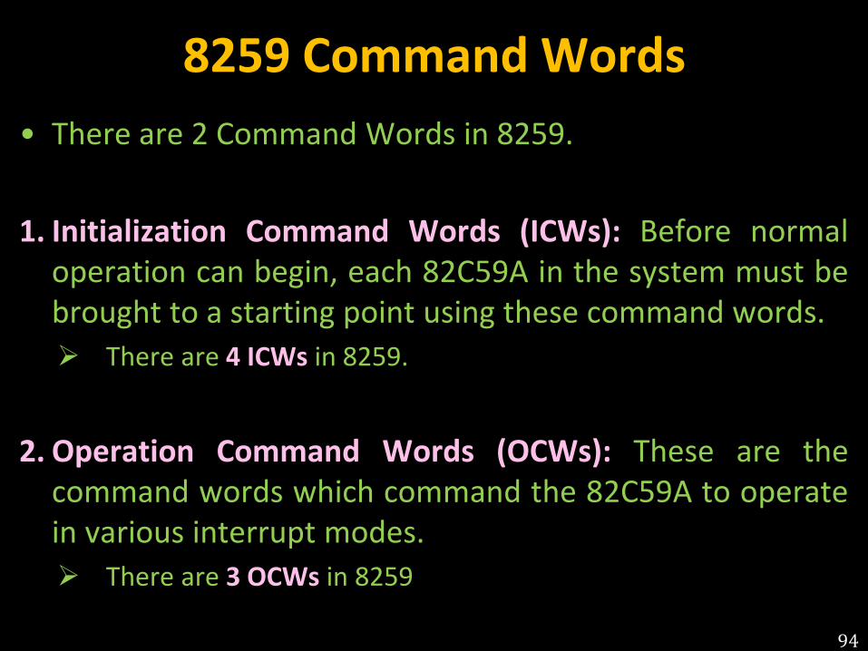
8259 Command Words
• There are 2 Command Words in 8259.
1. Initialization Command Words (ICWs): Before normal
operation can begin, each 82C59A in the system must be
brought to a starting point using these command words.
There are 4 ICWs in 8259.
2. Operation Command Words (OCWs): These are the
command words which command the 82C59A to operate
in various interrupt modes.
There are 3 OCWs in 8259
94
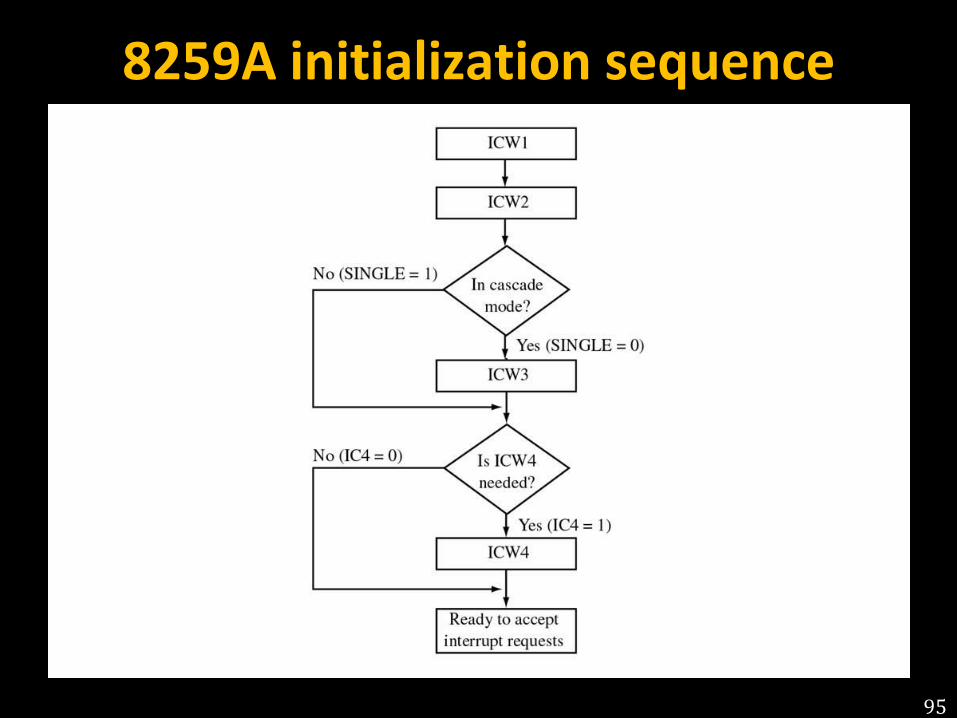
8259A initialization sequence
95
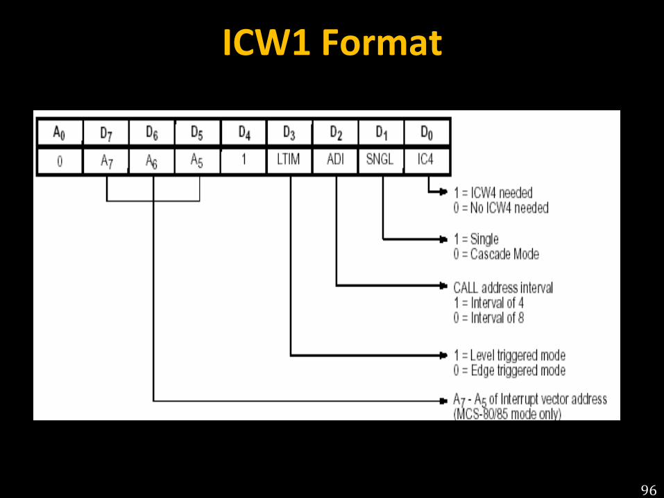
ICW1 Format
96
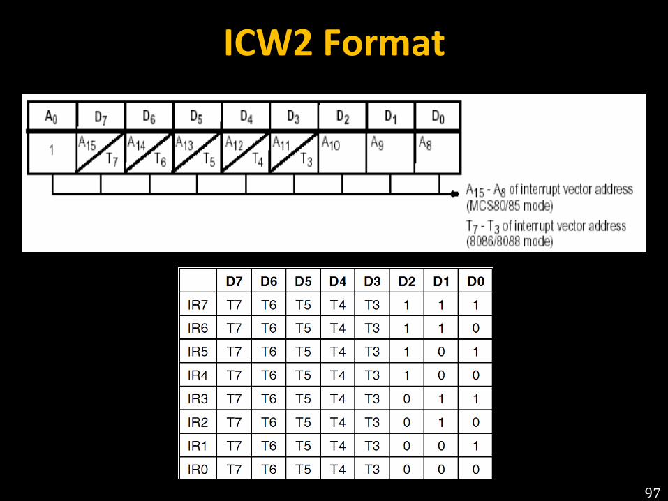
ICW2 Format
97
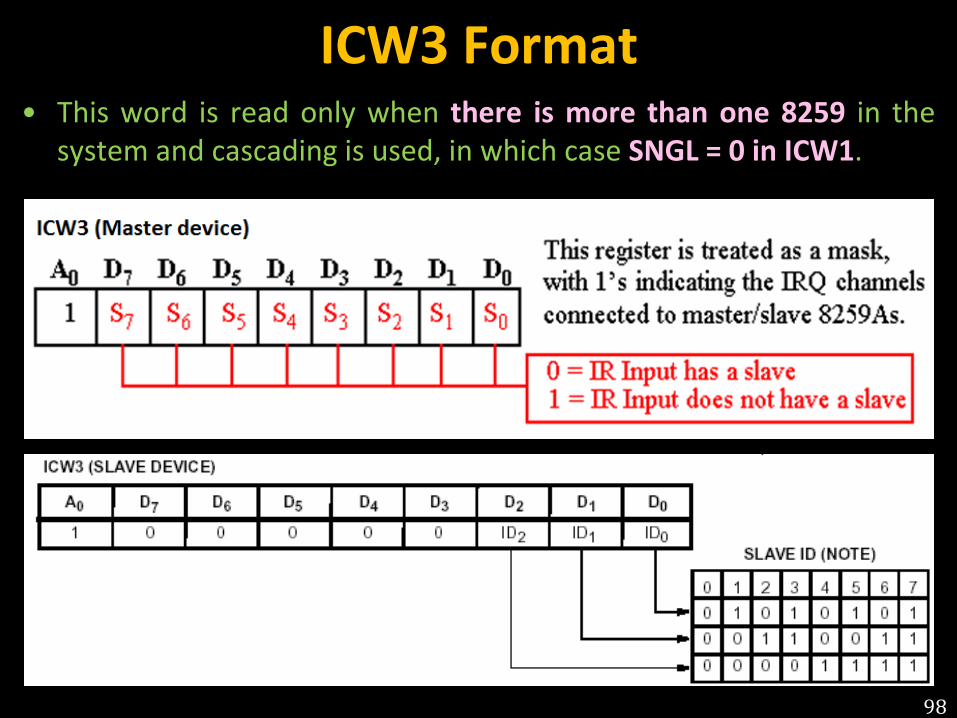
ICW3 Format • This word is read only when there is more than one 8259 in the
system and cascading is used, in which case SNGL = 0 in ICW1.
98
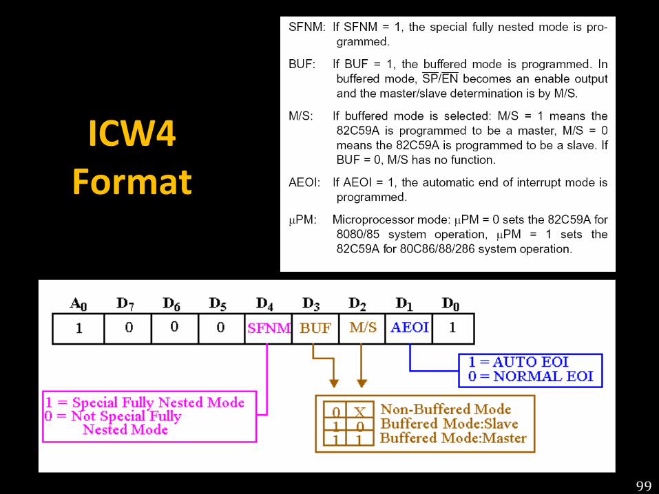
ICW4
Format
99
Operation Command Words (OCWs)
• After the Initialization Command Words (ICWs)
are programmed into the 8259A, the chip is ready
to accept interrupt requests at its input lines.
• However, during the 8259A operation, a selection
of algorithms can command the 8259A to operate
in various modes through the Operation
Command Words (OCWs).
100
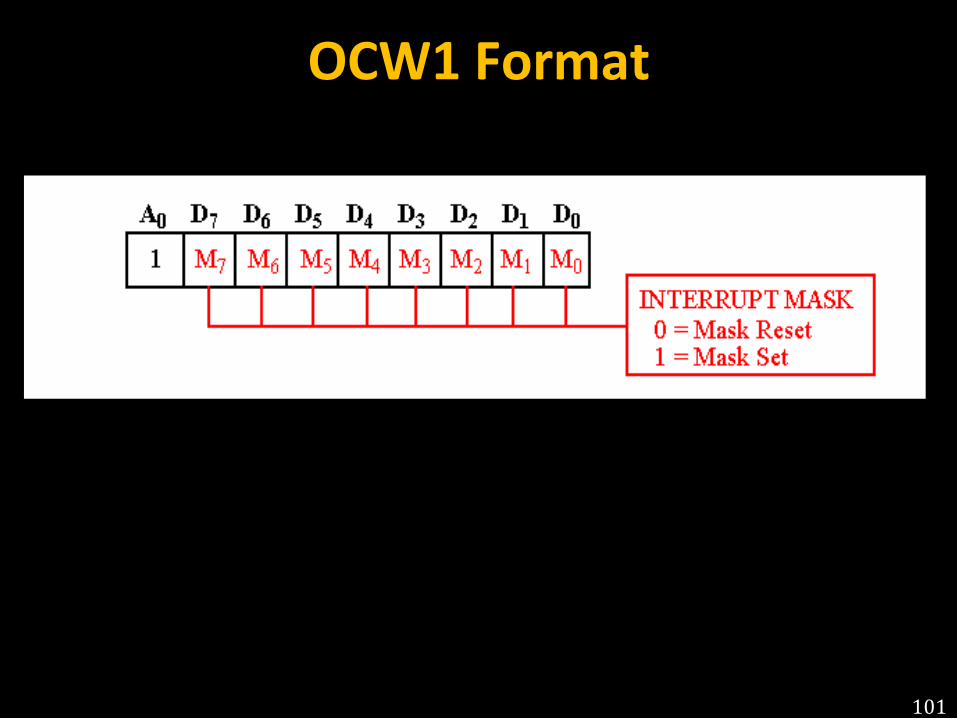
OCW1 Format
101
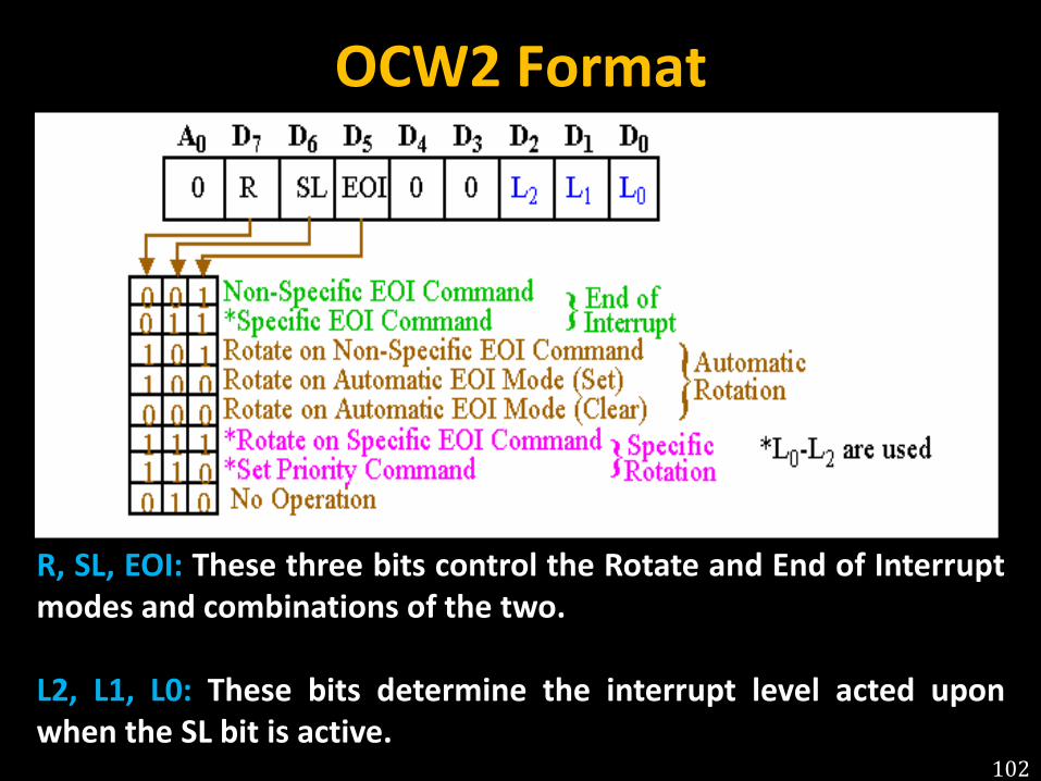
OCW2 Format
102
R, SL, EOI: These three bits control the Rotate and End of Interrupt
modes and combinations of the two.
L2, L1, L0: These bits determine the interrupt level acted upon
when the SL bit is active.
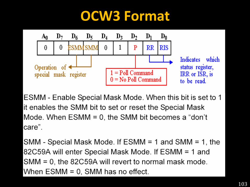
OCW3 Format
103
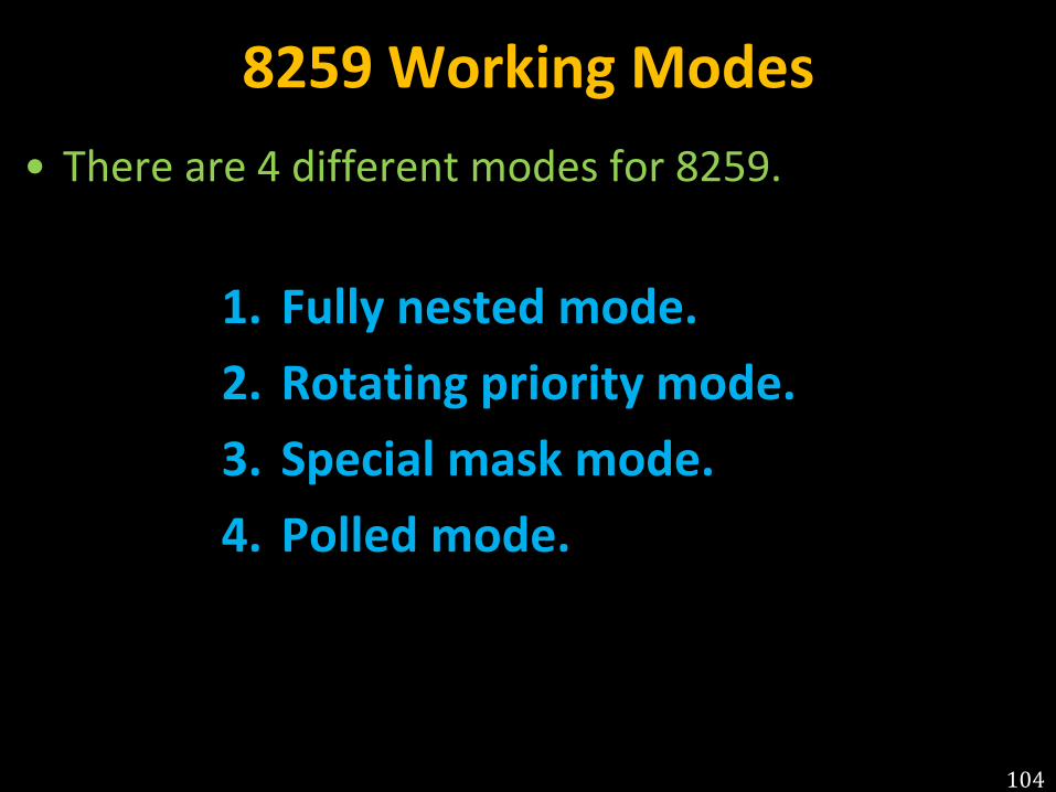
8259 Working Modes
• There are 4 different modes for 8259.
1. Fully nested mode.
2. Rotating priority mode.
3. Special mask mode.
4. Polled mode.
104
Fully nested mode
• This mode is entered after initialization unless another mode is
programmed.
• The interrupt requests are ordered in priority from 0 through 7 (0
highest).
• When an interrupt is acknowledged the highest priority request is
determined and its vector placed on the bus.
• Additionally, a bit of the Interrupt Service register (ISO-7) is set.
• This bit remains set until the microprocessor issues an End of
Interrupt (EOI) command immediately before returning from the
service routine
• If AEOI (Automatic End of Interrupt) bit is set, until the trailing edge
of the last INTA.
105
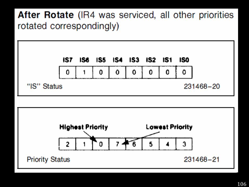
Rotating priority mode
• In some applications there are a number of interrupting
devices of equal priority.
• In this mode, a device after being serviced, receives the
lowest priority.
• So a device requesting an interrupt will have to wait, in the
worst case until each of 7 other devices are serviced at
most once .
106
Special mask mode
• Some applications may require an interrupt service routine to
dynamically alter the system priority structure during its execution
under software control.
• For example, the routine may wish to inhibit lower priority requests
for a portion of its execution but enable some of them for another
portion.
• That is where the Special Mask Mode comes in.
• In the special Mask Mode, when a mask bit is set in OCW1, it
inhibits further interrupts at that level and enables interrupts from
all other levels (lower as well as higher) that are not masked.
• Thus, any interrupts may be selectively enabled by loading the
mask register.
107
Polled mode
• In Polled mode the INT output functions as it normally
does.
• The microprocessor should ignore this output.
• This can be accomplished either by not connecting the
INT output or by masking interrupts within the
microprocessor, thereby disabling its interrupt input.
• Service to devices is achieved by software using a Poll
command.
• The Poll command is issued by setting P = 1 in OCW3. 108
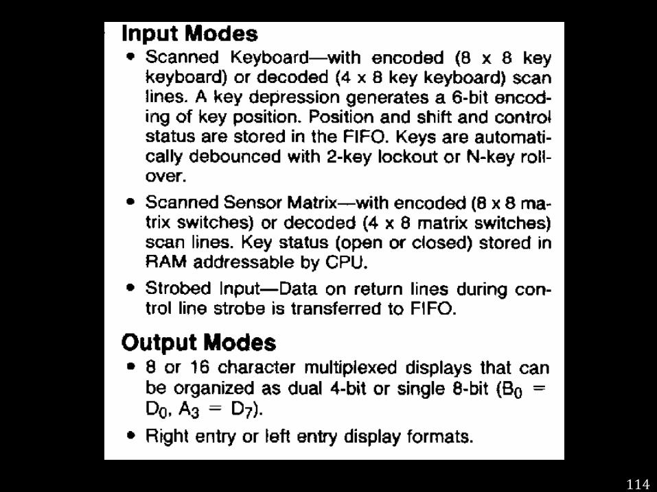
Features of 8279
• Scans and encodes up to a 64-key keyboard.
• Controls up to a 16-digit numerical display.
• Keyboard has a built-in FIFO 8 character buffer to
store the keyboard Entries and an Interrupt signal
with each Entry.
• The display is controlled from an internal 16x8
RAM that stores the coded display information.
110
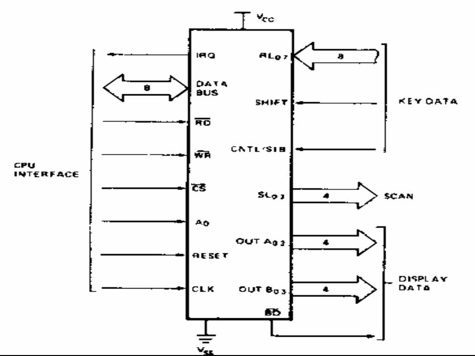
8279 Pin
Diagram
111
Pin Details
• A0 : Selects data (0) or control/status (1) for reads and
writes between microprocessor and 8279.
• BD : Output that blanks the displays.
• CLK : Used internally for timing. Maximum is 3 MHz
• CN/ST : Control/strobe, connected to the control key on the
keyboard.
• CS : Chip select that enables programming, reading the
keyboard, etc.
• DB7-DB0 : Consists of bidirectional pins that connect to data bus
on micro.
112
Pin Details
• IRQ : Interrupt request, becomes 1 when a key is
pressed, data is available.
• OUT A3-A0/B3-B0 : Outputs that sends data to the most
significant/least significant nibble of display.
• RD(WR) : Connects to micro's IORC or RD signal, reads
data/status registers.
• RESET : Connects to system RESET.
• RL7-RL0 : Return lines are inputs used to sense key
depression in the keyboard matrix.
• Shift : Shift connects to Shift key on keyboard.
• SL3-SL0 : Scan line outputs scan both the keyboard and
displays.
113
114
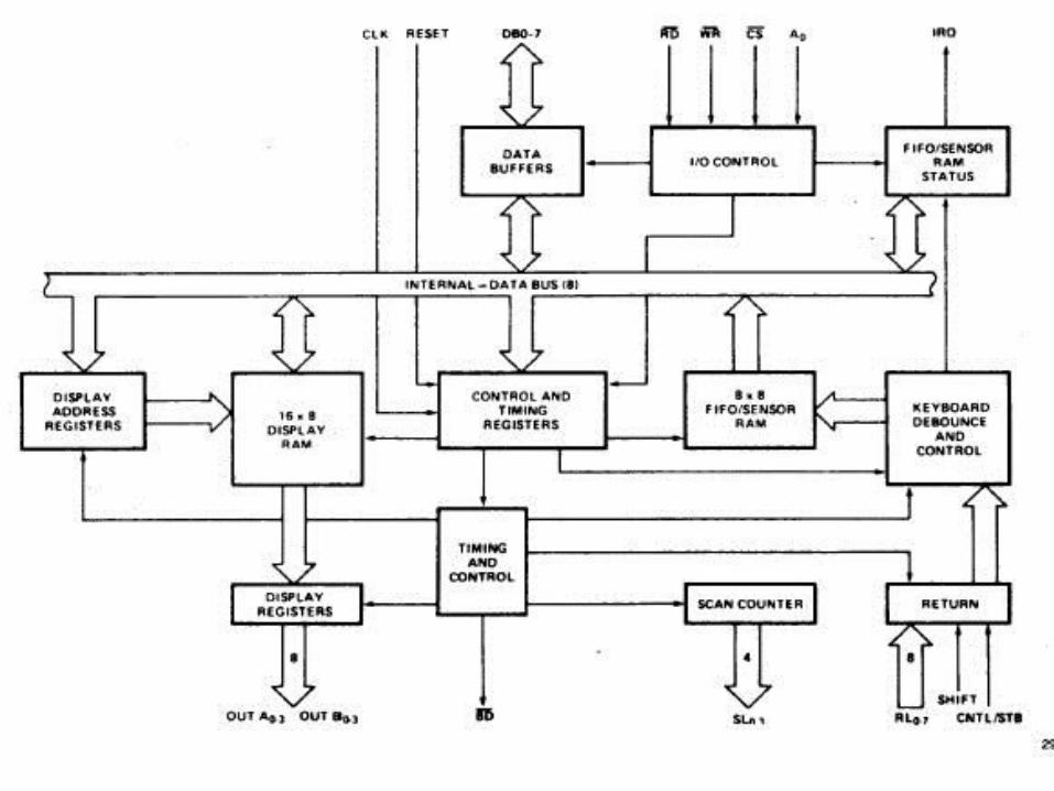
8279 Block Diagram
115
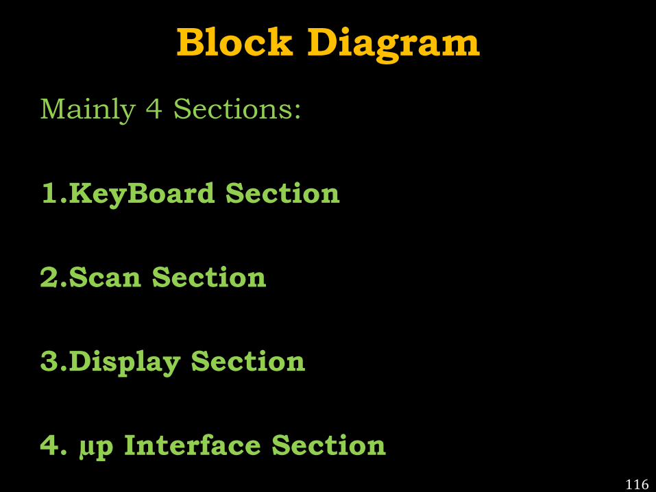
Block Diagram
Mainly 4 Sections:
1.KeyBoard Section
2.Scan Section
3.Display Section
4. µp Interface Section 116
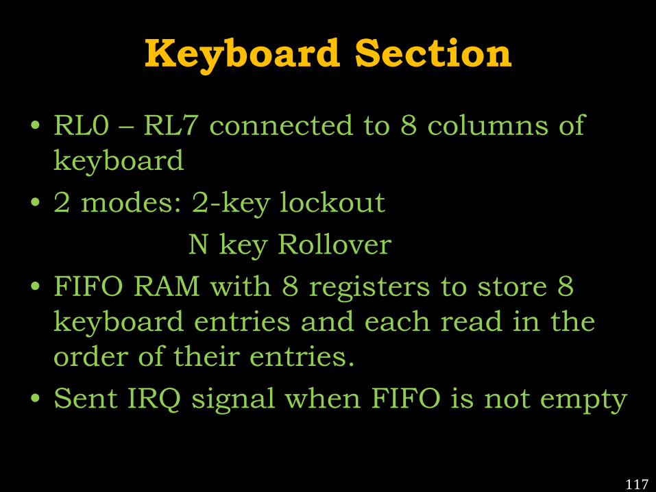
Keyboard Section
• RL0 – RL7 connected to 8 columns of
keyboard
• 2 modes: 2-key lockout
N key Rollover
• FIFO RAM with 8 registers to store 8
keyboard entries and each read in the
order of their entries.
• Sent IRQ signal when FIFO is not empty
117
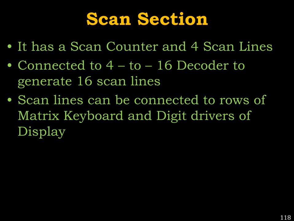
Scan Section
• It has a Scan Counter and 4 Scan Lines
• Connected to 4 – to – 16 Decoder to
generate 16 scan lines
• Scan lines can be connected to rows of
Matrix Keyboard and Digit drivers of
Display
118
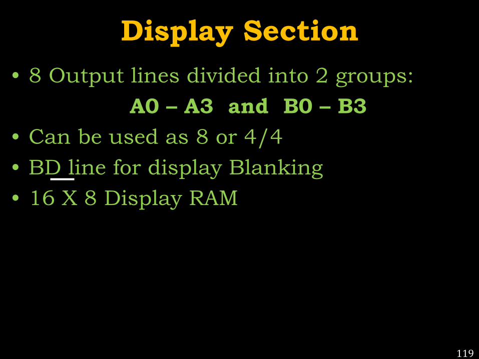
Display Section
• 8 Output lines divided into 2 groups:
A0 – A3 and B0 – B3
• Can be used as 8 or 4/4
• BD line for display Blanking
• 16 X 8 Display RAM
119
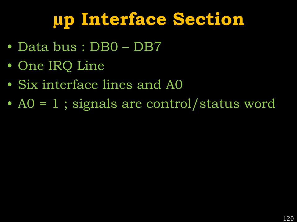
µp Interface Section
• Data bus : DB0 – DB7
• One IRQ Line
• Six interface lines and A0
• A0 = 1 ; signals are control/status word
120
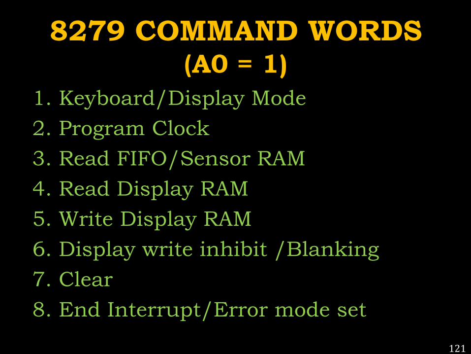
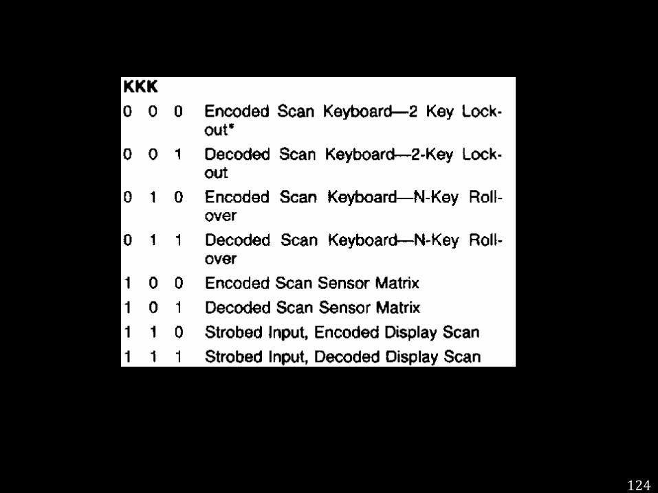
1. Keyboard/Display Mode
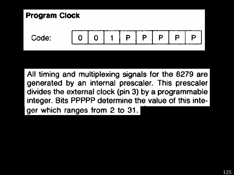
2. Program Clock
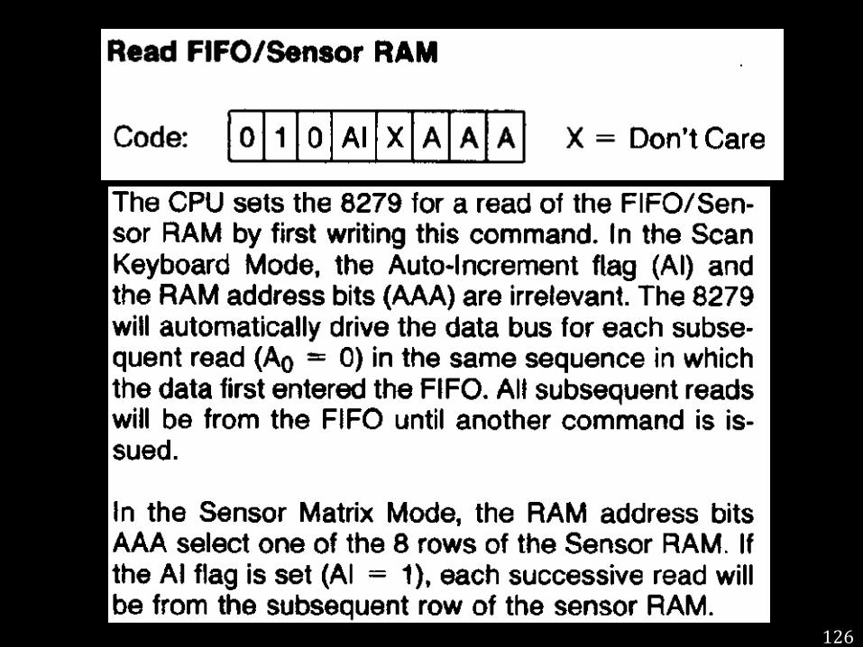
3. Read FIFO/Sensor RAM
4. Read Display RAM
5. Write Display RAM
6. Display write inhibit /Blanking
7. Clear
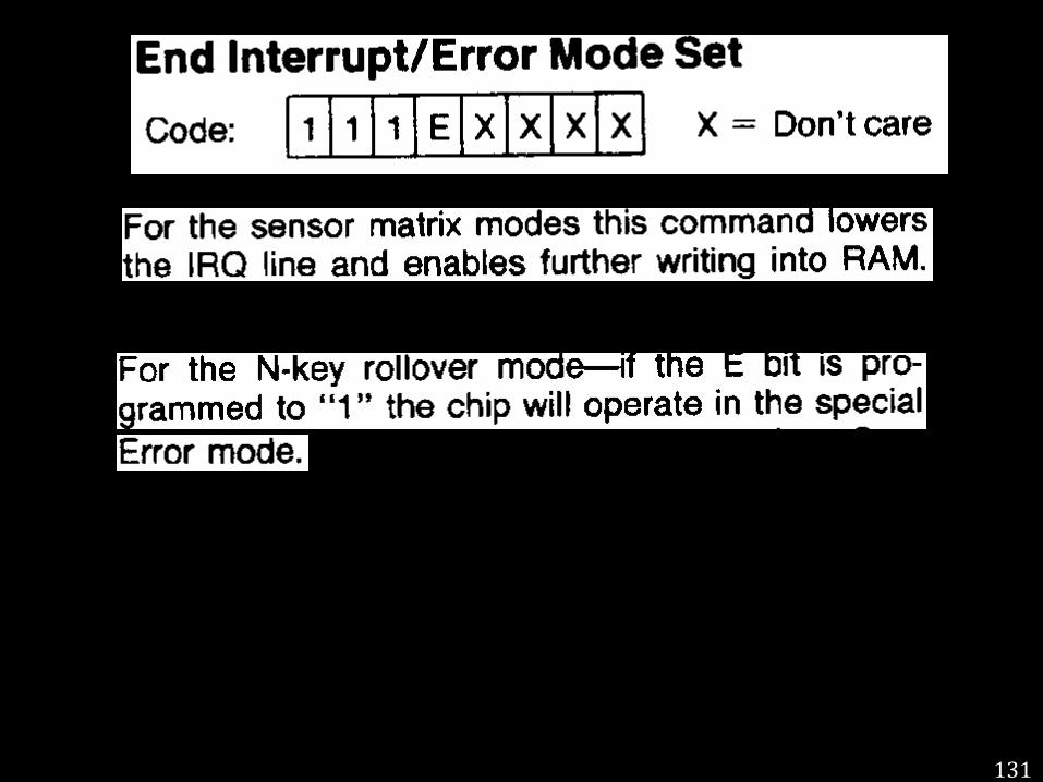
8. End Interrupt/Error mode set
8279 COMMAND WORDS (A0 = 1)
121
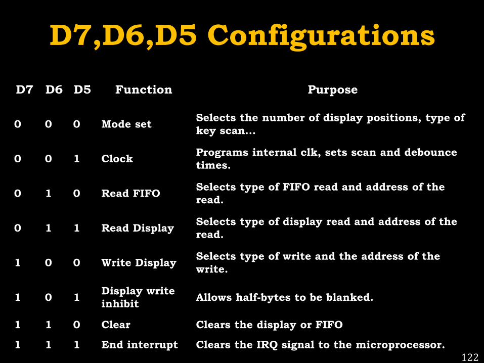
D7,D6,D5 Configurations
D7 D6 D5 Function Purpose
0 0 0 Mode set Selects the number of display positions, type of
key scan...
0 0 1 Clock Programs internal clk, sets scan and debounce
times.
0 1 0 Read FIFO Selects type of FIFO read and address of the
read.
0 1 1 Read Display Selects type of display read and address of the
read.
1 0 0 Write Display Selects type of write and the address of the
write.
1 0 1 Display write
inhibit Allows half-bytes to be blanked.
1 1 0 Clear Clears the display or FIFO
1 1 1 End interrupt Clears the IRQ signal to the microprocessor. 122
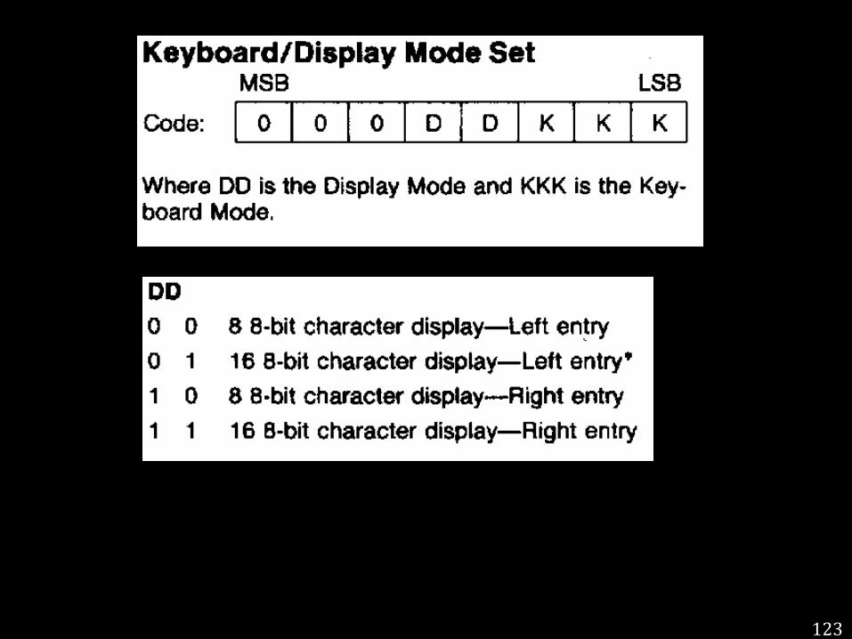
123
124
125
126
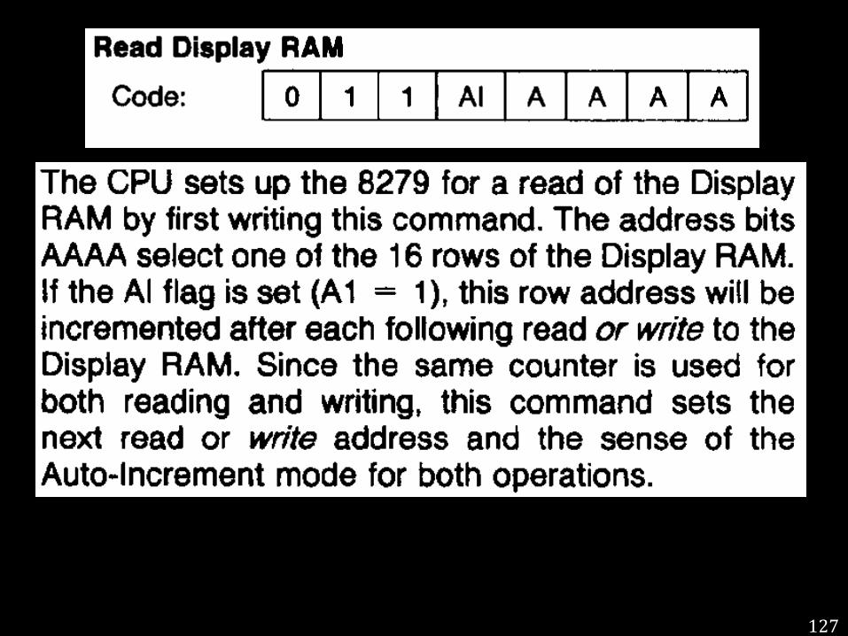
127
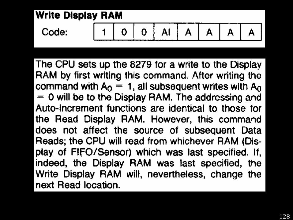
128
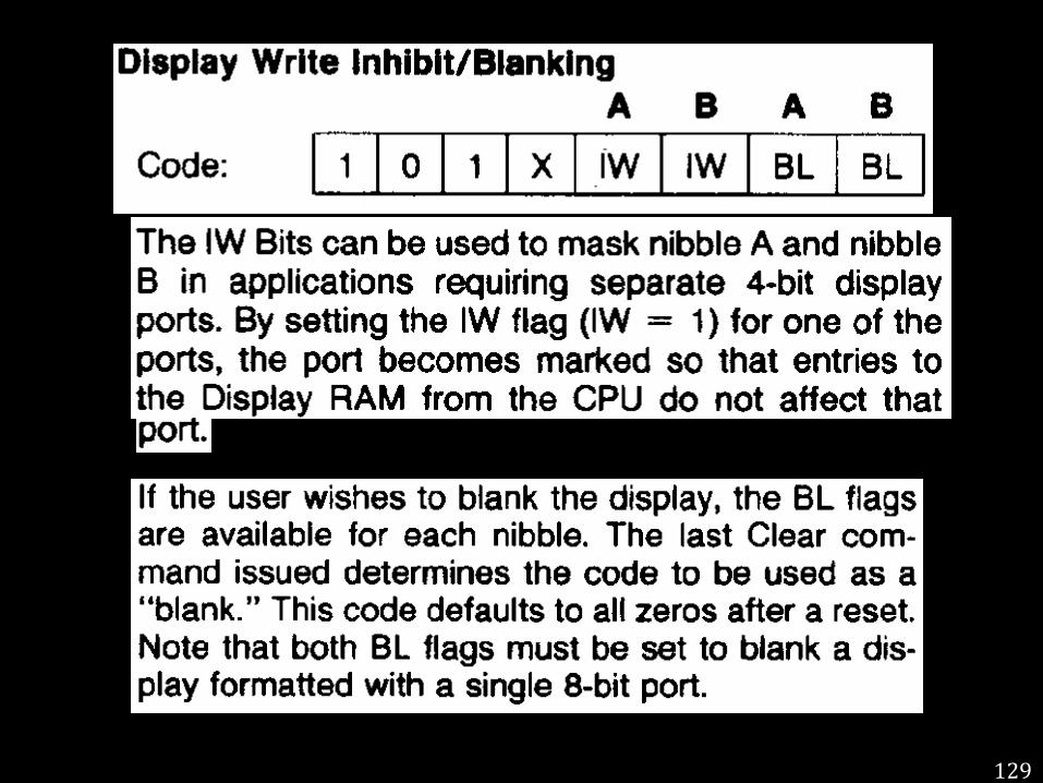
129
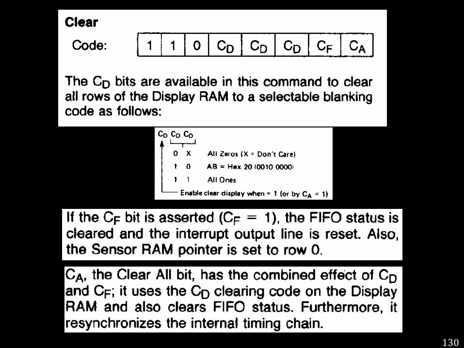
130
131
Related Documents