HAL Id: hal-03357106 https://hal.archives-ouvertes.fr/hal-03357106 Submitted on 28 Sep 2021 HAL is a multi-disciplinary open access archive for the deposit and dissemination of sci- entific research documents, whether they are pub- lished or not. The documents may come from teaching and research institutions in France or abroad, or from public or private research centers. L’archive ouverte pluridisciplinaire HAL, est destinée au dépôt et à la diffusion de documents scientifiques de niveau recherche, publiés ou non, émanant des établissements d’enseignement et de recherche français ou étrangers, des laboratoires publics ou privés. Digital-to-Analog Hardware Trojan Attacks Mohamed Elshamy, Giorgio Di Natale, Alhassan Sayed, Antonios Pavlidis, Marie-Minerve Louërat, Hassan Aboushady, Haralampos-G. Stratigopoulos To cite this version: Mohamed Elshamy, Giorgio Di Natale, Alhassan Sayed, Antonios Pavlidis, Marie-Minerve Louërat, et al.. Digital-to-Analog Hardware Trojan Attacks. IEEE Transactions on Circuits and Systems I: Regular Papers, IEEE, inPress, pp.1-14. hal-03357106

Welcome message from author
This document is posted to help you gain knowledge. Please leave a comment to let me know what you think about it! Share it to your friends and learn new things together.
Transcript
HAL Id: hal-03357106https://hal.archives-ouvertes.fr/hal-03357106
Submitted on 28 Sep 2021
HAL is a multi-disciplinary open accessarchive for the deposit and dissemination of sci-entific research documents, whether they are pub-lished or not. The documents may come fromteaching and research institutions in France orabroad, or from public or private research centers.
L’archive ouverte pluridisciplinaire HAL, estdestinée au dépôt et à la diffusion de documentsscientifiques de niveau recherche, publiés ou non,émanant des établissements d’enseignement et derecherche français ou étrangers, des laboratoirespublics ou privés.
Digital-to-Analog Hardware Trojan AttacksMohamed Elshamy, Giorgio Di Natale, Alhassan Sayed, Antonios Pavlidis,Marie-Minerve Louërat, Hassan Aboushady, Haralampos-G. Stratigopoulos
To cite this version:Mohamed Elshamy, Giorgio Di Natale, Alhassan Sayed, Antonios Pavlidis, Marie-Minerve Louërat,et al.. Digital-to-Analog Hardware Trojan Attacks. IEEE Transactions on Circuits and Systems I:Regular Papers, IEEE, inPress, pp.1-14. �hal-03357106�
1
Digital-to-Analog Hardware Trojan AttacksMohamed Elshamy, Giorgio Di Natale, Senior Member, IEEE, Alhassan Sayed, Antonios Pavlidis, Marie-Minerve
Louerat, Hassan Aboushady, Senior Member, IEEE, and Haralampos-G. Stratigopoulos, Member, IEEE
Abstract—We propose a Hardware Trojan (HT) attack foranalog circuits with its key characteristic being that it cannot beprevented or detected in the analog domain. The HT attack worksin the context of Systems-on-Chip (SoCs) comprising both digitaland analog Intellectual Property (IP) blocks. The attacker couldbe either the SoC integrator or the foundry. More specifically,the HT trigger is placed inside a dense digital IP block whereit can be effectively hidden, whereas the HT payload is inthe form of a digital pattern transported via the test bus orgenerated within the test bus, reaching the Design-for-Test (DfT)or programmability interface of the victim analog IP with the testbus. The HT payload unexpectedly activates the DfT and sets thevictim analog IP into some possibly partial and undocumentedtest mode or changes the nominal programmability. The HTpayload can be designed to result in performance degradationor complete malfunction, i.e., denial of service. We demonstratethis HT attack scenario on two analog IPs, namely a low-dropout(LDO) regulator using simulation and an RF receiver usinghardware measurements.
Index Terms—Hardware security and trust, hardware Trojans,test access and control mechanisms, analog and mixed-signalintegrated circuits.
I. INTRODUCTION
The globalization of the Integrated Circuit (IC) design andfabrication steps has introduced an horizontal IC design modelwhere the design of a single chip involves many differentparties, i.e., Computer-Aided Design (CAD) tool providers,Intellectual Property (IP) block providers, System-on-Chip(SoC) integrators, foundries, etc. As a result, the IC designtravels through many parties which introduces many pointswhere an attack may be staged. Attack scenarios includecloning, counterfeiting, IC overbuilding, reverse engineering,and Hardware Trojan (HT) insertion. This work deals withHT attacks which are a major preoccupation for society,industry, governments, and military, since they pose severerisks with possibly disastrous outcomes. For this reason, HTshave received major attention in the scientific communitythroughout the last two decades [1], [2].
Manuscript received April 12, 2021; revised July 24, 2021, and August 30,2021; accepted September 16, 2021. This work was supported by the ANRSTEALTH project under Grant ANR-17-CE24-0022-01 and by the RAPIDFLEXyRADIO project. This article was recommended by Associate Editor P.Rombouts. (Corresponding author: Haralampos-G. Stratigopoulos.)
Mohamed Elshamy, Antonios Pavlidis, Marie-Minerve Louerat,Hassan Aboushady, and Haralampos-G. Stratigopoulos are withthe Sorbonne Universite, CNRS, LIP6, 75005 Paris, France(e-mail: [email protected]; [email protected];[email protected] [email protected]; [email protected]).
Giorgio Di Natale is with the Universite Grenoble Alpes, CNRS, TIMA,38000 Grenoble, France (e-mail: [email protected]).
Alhassan Sayed is with the Sorbonne Universite, CNRS, LIP6, 75005 Paris,France, and also with the Electronics and Communications Department, MiniaUniversity, Minia 61519, Egypt (e-mail: [email protected]).
Digital Object Identifier 10.1109/TCSI.2021.XXXXXXX
A HT is a malicious modification of the design performedby an attacker within the IC supply chain that is intent to stayhidden and evade detection by the end-user who is the defenderin this case. The HT is an undocumented functionality for theend-user and is designed in such a way that once activated itis capable of performing an undesired effect for the end-user.The motivation for inserting a HT includes leaking sensitiveinformation out of the chip, e.g., cipher keys, degrading theperformance of the chip, or leading to complete malfunction,e.g., denial-of-service.
Any HT is in general composed of a trigger and a payloadmechanism. The HT may be always-on, in which case strictlyspeaking there is no trigger mechanism, it may be uncontrol-lably activated based on some rare conditions occurring, or itmay have a well-timed activation controlled by the attackerleaving a time bomb into the design. The payload mechanismrefers to the HT effect on the chip’s functionality.
In addition to the HT activation mechanism and HT effect,a commonly used taxonomy of HTs considers the insertionphase, the abstraction level, and the HT location on the die.A HT may be inserted by the CAD tool provider, i.e., bycompromising the synthesis or verification scripts, by an IPdesign team, by a SoC integrator that can manipulate boththe third-party IP (3PIP) cores and the test infrastructurecomprising the test access and control mechanism and severalembedded test instruments, and by a foundry that receives theGDSII file. A HT may be inserted at system-level, register-transfer level (RTL), gate-level, or layout-level. The locationof the HT could be anywhere on the die, i.e., digital processor,memory, power management unit, analog cores, etc.
There is a multitude of HT designs proposed in the literaturethat range from simple to very complex attack modes. Thesimplest HTs are combinational circuits that monitor a set ofnodes to generate a trigger on the simultaneous occurrenceof rare node conditions and, subsequently, once the trigger isactivated, the payload is simply flipping the value of anothernode. Another category of simple HTs are the sequentialHTs which also have a condition-based activation, but theyare triggered with a sequence of conditions and not with aspecific state or condition like the combinational HTs. Morecomplex HTs include silicon wearout mechanisms [3], hiddenside-channels [4], changing dopant polarity in active areas oftransistors [5], siphoning charge from victim wires [6], etc.
From the attacker’s perspective, the goal is to achieve thedesired effect via the use of a stealthy and minimum footprintHT such that it evades pre-silicon prevention and post-silicondetection methods applied by the defender.
Pre-silicon prevention methods include: (a) functional veri-fication of 3PIP cores [7]; (b) structural analysis of HardwareDescription Language (HDL) codes [7]; (c) targeted automatic

2
test pattern generation algorithms [8] or simulating the circuitusing specific test benches, i.e., performing aging simulationsalong with over-clocking [9] or short-term aging [10] to mag-nify the effect of the HT without triggering it; (d) searchingfor unused components during design-time verification andremoving them as potentially suspicious [11]; (e) filling in allunused spaces on the layout, which are most likely insertionareas for HTs, with functional filler cells and checking if thosehave changed [12]; and (f) design obfuscation, for exampleusing locking [13], [14], camouflaging [15], [16], or splitmanufacturing [17], aiming at obscuring the IC functionalityso as to make it difficult for the attacker to insert the HT.
Post-silicon detection methods include: (a) destructivereverse-engineering, which involves de-packaging and de-layering the chip, imaging the chip’s layers, and using softwareto stitch together the prepared images, thereby recovering thelayout and netlist, which thereafter can be carefully examinedto detect the presence of HTs [18], [19]; (b) optical circuitanalysis aiming at measuring optical emissions of the ICand comparing them with a trusted emission image of a“golden” IC [20]; (c) functional testing aiming at exposing theHT by applying test patterns [8]; (d) statistical side-channelfingerprinting aiming at exposing the HT by its effect onparametric measurements, i.e., delay, power, temperature, etc.[21], [22]; and (e) using run-time monitors, i.e., current sensors[23] and thermal sensors [24].
To date, the vast majority of HT attacks and defenseshave been demonstrated for digital ICs [25]. Few HT designshave been demonstrated in the analog domain, including HTsinserted into the RF front-end aiming at leaking sensitiveinformation via a covert side-channel [26]–[29] and HTs thatbring the analog IC into an undesired state or operation mode[30]–[34]. The prior art on HT in the analog domain will bereviewed in more detail in Section II.
In general, designing HTs for analog ICs is very challengingsince all criteria that make up an effective HT are difficultto meet. First, it is difficult to design stealthy HT sinceanalog signal paths are typically very sensitive and a HTcircuitry tapping into them is likely to result in some non-negligible performance degradation, thus it will be difficult forthe infected IC to pass testing. Second, it is difficult to designsmall footprint HTs that will evade optical reverse engineeringsince analog designs comprise few components or can beclearly divided into sub-blocks or stages each comprising fewcomponents. Third, on any analog IC we can extract severalinformation-rich measurements, such that it is unlikely not tobe able to find a measurement subspace wherein the statisticalfingerprints of HT-infected and HT-free instances are clearlydistinguished.
In this paper, we propose a HT attack for analog ICswith its key characteristic being that it is invisible in theanalog domain [35]. This is achieved by exploiting the on-chip test infrastructure that is common to digital and analogcores within the SoC. In particular, the HT trigger mechanismresides in a digital IP core and the payload mechanism residesin the test bus that links all IP blocks in the SoC in a daisynetwork. The HT is triggered in the dense digital section ofthe SoC, thus posing challenge for HT prevention or detection.
The HT payload is transferred to the victim analog IP viathe test bus and the interface of the analog IP to the testbus. The interface can include Design-for-Test (DfT) blocks,i.e., sensors and actuators, and programmability fabric for thepurpose of calibration. The proposed HT is demonstrated ontwo case studies. The first case study shown with simulationis a low-dropout (LDO) regulator where the HT infects it viaits DfT interface. The second case study shown with hardwaremeasurements is an RF receiver front-end where the HT infectsit via its programmability fabric.
The rest of the paper is structured as follows. In Section II,we review the prior art on HT attacks in the analog domain.In Section III, we provide an overview of DfT techniques forAnalog and Mixed-Signal (A/M-S) and RF ICs. In SectionIV, we provide an overview of calibration schemes present inA/M-S and RF ICs. In Section V, we review a modern testinfrastructure and its use for accessing and controlling DfTstructures and the programmability fabric. In Section VI, wepresent the proposed HT attack scenarios. In Sections VII andVIII, we demonstrate the HT attack on the two case studies.Section IX concludes the paper.
II. PRIOR ART ON HT ATTACKS IN THE ANALOG DOMAIN
In [26]–[29], HT attacks are demonstrated for wireless ICsaiming at leaking secret information within a legitimate signaltransmission. The attacker leverages the data transmissioncapability of the HT-infected device to establish a covertside-channel, without the need to gain physical access tothe device. For example, the HT could forward bit-by-bitthe content of the cipher key register of the crypto-core tothe analog transmitter. In [26], [27], [29], the idea is toexploit the margins that exist between the operating point ofthe transmitter and the boundaries defined by the transmitterand communication standard specifications. In particular, theHT performs minute modifications in the parameters of thetransmitted signal, such as amplitude and frequency, to leaksensitive information from the tampered device. Two HT pay-load mechanisms are shown in [29], one that uses a single poledouble throw switch and a pair of resistors to alter the inputtermination impedance of the power amplifier, and anotherone that reprograms the gain stages. In [28], it is proposedto use spread spectrum techniques to hide an unauthorizedtransmission signal within the legitimate signal below thenoise level. For all the aforementioned HT attacks, the ICpasses all conventional specification tests and the transmissionsignal still obeys the transmission specifications and is withinthe margins allowed because of process variations. Therefore,the inconspicuous receiver cannot interpret the minute changein the transmitted signal as malicious. However, the attackerknowing the HT payload mechanism can listen to the channeland recover the key. It has been demonstrated that this type ofHTs can be detected by statistical side-channel fingerprinting[27], careful analysis of the transmitted signal spectrum [28],or adaptive channel estimation [29], which leverages the slow-fading characteristics of indoor communication channels todistinguish between channel impairments and HT activity.
Another interesting direction for HT design is to exploitthe fact that an analog IC may have undesired states or

3
operation modes. In this case, the HT attack consists ofbringing the analog IC into one of these states to causeundesirable operation. This HT type has been demonstrated fora multitude of basic analog circuits, such as current mirrors,filters, oscillators, bandgap reference sources and operationalamplifiers [30]–[34].
III. DFT FOR A/M-S AND RF ICS
DfT consists in embedding test structures on-chip with theaim to improve defect coverage and/or facilitate testing, i.e.,reduce the test cost by speeding up test application timeand/or alleviating the dependence on complex Automatic TestEquipment (ATE). Built-in Self-test (BIST) is a special formof DfT where the test procedure takes place entirely on-chipwithout needing to interface the chip to external ATE. In post-manufacturing testing, BIST can offer significant test costsavings at the expense of larger area overhead. For safety-critical or mission-critical applications, it can be reused inthe field of operation to perform on-line test in idle timesor concurrent error detection.
In general, for A/M-S and RF ICs, the DfT circuitry cancomprise one or more of the following test structures: testaccess points, digitally-controlled re-configuration schemes,and test instruments, i.e., test stimulus generators, actuators,sensors, checkers, and test response analyzers.
Examples of generic DfT techniques include oscillation-based testing [36], topology modification [37], and symmetry-based BIST [38]. In oscillation-based testing, the circuit isre-configured in a positive feedback loop to force oscillation.Then, the oscillation frequency and amplitude are measuredon-chip using as test response analyzer a counter and am-plitude detector, respectively. Deviations from the nominalexpected oscillation frequency and amplitude point to defectdetection. In topology modification, 1-bit controlled Pull-Down (PD) and Pull-Up (PU) transistors are used to tie a nodeto Vdd or ground, respectively, with the aim of re-configuringthe circuit such that defects are better exposed. In symmetry-based BIST, invariant properties, i.e., properties that hold truein error-free operation but are violated in the presence ofdefects, are built and monitored by checkers.
There exist also DfT techniques that are specific to thecircuit class, i.e., linear time-invariant circuits, Phase-LockedLoops (PLLs), data converters, RF transceivers, etc., andoftentimes specific to different architectures within a circuitclass.
For linear time-invariant circuits, concurrent error detectionis achieved by checkers that monitor checksums [39] or createa pseudo-duplicated response that by default in error-freeoperation converges to the circuit output [40].
For Analog-to-Digital Converters (ADCs), traditional BISTschemes for static linearity testing, i.e., Differential Non-Linearity (DNL) and Integral Non-Linearity (INL), use teststimulus generation performed by ramp generators [41] anda test response analyzer that computes the histogram [42],which could be done also based on reduced-code collection[43]. The requirement for a high-resolution test stimulus canbe relaxed by using non-linear stimulus generators combined
with advanced post-processing techniques of the converter’soutput [44]. Traditional BIST schemes for dynamic testing,i.e., Signal-to-Noise Ratio (SNR), use test stimulus generationperformed by sinusoidal signal generators [45], [46] or Σ∆bitsteams encoding sinusoidal signals [47], and test responseanalyzers that perform spectral analysis [48] or sine-wavefitting analysis [47].
For PLLs, BIST techniques have been proposed for measur-ing on-chip the jitter [49], [50]. The PLL response is under-sampled and the count of unstable bits at the clock risingedges is correlated to the high-frequency jitter. Defect-orientedBIST for PLLs has been proposed in [51], where a digitalPseudo-Random Bit Sequence (PRBS) injected in the chargepump perturbs the PLL, and the cross-correlation of the PRBSpattern with the output of the phase/frequency detector isconsidered for defect detection.
For RF transceivers, a common BIST technique consists increating a loop-back connection between the transmitter andthe receiver, in order to test the whole RF transceiver, e.g.,measure the Error Vector Magnitude (EVM), using basebandonly signals [52], [53].
Sensor-based testing is another common DfT technique.Current sensors [54] and amplitude detectors [55] can be usedto monitor current or voltage on internal nodes. There existalso non-intrusive sensors that extract information withoutbeing electrically connected to the circuit under test, e.g.,temperature sensors [56] and process variation-aware sensors[57].
IV. CALIBRATION OF A/M-S AND RF ICS
Calibration schemes are oftentimes utilized in A/M-S andRF ICs with the aim of boosting yield, i.e., by compensatingagainst process variations and non-idealities, and to programdifferent operation modes, e.g., in the case of multi-standardRF transceivers [58], [59]. Embedding calibration in A/M-Sand RF ICs becomes essential especially in advance tech-nology nodes since such designs suffer from yield loss dueto model immaturity and variability caused by parasitics andlayout-dependent effects.
At a minimum, a calibration scheme utilizes digitally-controlled tuning knobs that act on the circuit performances.Tuning knobs may include bias voltages, current sources, orsingle tunable components, such as resistors, capacitors, andvaractors.
The standard calibration algorithm consists in multipletesting/tuning iterations where in each step the performancesare measured and the next best tuning knob setting is dictatedbased on some optimization algorithm.
The calibration scheme may also utilize on-chip sensors forperformance measurement which can speed-up the test cycleand alleviate the dependence on complex ATE. For example,one-shot calibration schemes based on process-variation-awaresensors and machine learning are proposed in [60], [61].
The most advance calibration schemes are fully imple-mented on-chip rendering the circuit self-healing. Theseschemes can also be used during the lifetime of the circuit tocompensate against aging. They comprise tuning knobs or ac-tuators, sensors for extracting information-rich measurements

4
Fig. 1: Scan access including analog IPs (adapted from [64]).
or directly the performances, and a digital processor enginethat maps the outputs of the sensors to tuning knob valuesand aims at driving the optimization so as to identify a goodbalance among multiple competing performance goals [62],[63].
V. TEST ACCESS AND CONTROL MECHANISM IN SOCS
A modern SoC can embed numerous IP blocks and, in turn,each IP block typically embeds a variety of DfT structures,i.e., test access points and test instruments, and comes with acalibration scheme that uses a programmability interface. Thetotal number of DfT structures and tuning knobs in a SoCcan easily be in the order of hundreds or even thousands, andaccessing them separately from primary pins is prohibitive.
To this end, an on-chip test infrastructure is used thatconnects all the DfT structures and programming interfaces toa common test bus, in order to gain access and control them,manage the test and calibration process, and offload the testresponse to the ATE for off-chip test response analysis, all-in-all using a limited number of dedicated primary pins [65]. Thetest bus is interfaced on the chip boundary with the test accessport (TAP). Typically, each IP block has its own test program,i.e., IP-level test patterns, and once the SoC design is finalizedand the test infrastructure is added, the test programs are re-targeted to the top-level design. The test programs can besimply concatenated, but to achieve higher test time efficiencythey can be regrouped enabling concurrency.
The test infrastructure is standardized driven by the needsfor test portability and re-use [65]. Portability refers to reusinga test program independently of the position of the target
IP block inside the SoC hierarchy, reusing a test programat different steps, i.e., post-manufacturing test, debugging, in-field test towards dependable designs, etc., and reusing a testprogram independently of the ATE platform. Standardizationdissociates the IP block-level DfT structure and programminginterface design from test application and calibration oper-ations at SoC-level, i.e., access, control, observe, program,etc., and allows all actors, i.e., IP providers, SoC integrators,test infrastructure providers, to speak the same language. Italso enables test automation using CAD tools and leads tosignificant SoC-level test time reduction.
The latest standard for test infrastructure controllability andobservability is the IEEE Std. 1687 [66]. It deals with the greatnumber of DfT structures and connects them serially via pro-grammable segment insertion bits (SIBs) to a reconfigurablescan network (RSN) between the scan in (SI) and scan out(SO) ports. When the SIB of a DfT structure is opened, itstest data register (TDR) becomes part of the RSN such that itis accessed from the SI port and its output is streamed to theSO port.
IEEE Std. 1687 was developed with digital ICs in mind. Thestandard for analog test access is the IEEE Std. 1149.4 [67]and dates from the 1990s. It proposes a test bus paradigm thatis still used today, but it requires a minimum of two additionaltest pins which is too costly and often prohibitive as manydesigns are pin-limited. To this end, nowadays there is anIEEE working group extending IEEE Std. 1687 [68] to includeproperties demanded by analog ICs, such as periodic sampling.The envisioned test access standard will be compatible forboth analog and digital IPs in a SoC connecting them onto acommon test infrastructure.
The principle for connecting analog IPs to the common testinfrastructure is proposed in [64]. An example is shown in Fig.1, depicting two analog IPs and several digital IPs connected toa common scan path. For simplicity, the SIBs are not included.To be able to connect analog IPs to the test infrastructure itis required that analog test stimuli and analog test responsesare first digitized. This is achieved by using on-chip Digital-to-Analog Converters (DACs) and ADCs, respectively, whichcould be shared among several analog IPs if these are testedsequentially and the voltage ranges are consistent. Four typesof connections to the scan path are shown in Fig. 1 foranalog IPs: (a) a DAC connecting an analog node insidethe IP or the DfT structure, e.g., for forcing an analog teststimulus; (b) an ADC connecting an analog node inside theIP or the DfT structure, e.g., for monitoring a test responsesignal; (c) a direct connection to the DfT, e.g., for activating adigitally-controlled re-configuration scheme or embedded testinstrument; and (d) a direct connection to the digital tuningknobs used for calibration. Fig. 1 shows for simplicity 3-bit data converters and 3-bit words controlling the tuningknobs and DfT structures, but in fact any TDR size can beaccommodated into the scan path. It also shows a numberof intervening or appended TDRs that connect digital IPs tothe scan path, as well as the case where an analog signalinside an analog IP is digitized via the ADC and driven intoa digital IP and the case where the output of a digital IPis converted via the DAC to analog and drives an analog

5
Fig. 2: HT scenario exploiting the SoC test infrastructure.
input of the analog IP. Finally, Fig. 1 shows the three maincontrol signals, namely shift, update, and capture. The shiftoperation shifts the data serially through the scan path one bitper clock cycle. The update operation latches the data to theinput of the ADC, to the input of the DfT structure, or to theprogramming bits of the tuning knobs. The capture operationoffloads a digitized test response into the scan path to bescanned out for subsequent off-chip analysis. For each ADCand DAC, a counter and a packet size register are used thatset the periodicity of the TDR update and capture operations.For a more detailed description of the test infrastructure, theinterested reader is referred to [64].
VI. PROPOSED HT ATTACK
A. Threat Model
We assume that the attacker has access to the SoC designand can manipulate a digital IP and the test infrastructure. Theattacker also needs to have some minimum knowledge of thevictim analog IP so as to design the HT payload. Based onthis threat model, the attacker could be the SoC integrator orthe foundry.
B. Attack scenario
It is well-known that the test infrastructure can be a vehiclefor attacks. From a general point of view, such attacks can becategorized into external threats and internal threats. Externalthreats consider an unauthorized user that gains control of thechip via the TAP. They include launching several types of scanattacks aiming at stealing secret keys [69], [70], performingreverse-engineering and device cloning [71], performing mem-ory dumping [72], and modifying memory values to attainprivilege escalation [73]. Internal threats consider that theattack takes place entirely inside the chip. For example, athird-party malicious IP connecting to the scan network canaim at sniffing confidential data or can act as a tamperingIP corrupting the test data of another IP as they are beingtransported across the scan network [74]. For a more detaileddescription and a taxonomy of security threats in IEEE teststandards, the interested reader is referred to [75].
In this paper, we propose a novel HT attack scenario wherethe test infrastructure is a vehicle for infecting an analog IP.
The HT attack, illustrated in Fig. 2, exploits the fact that analogand digital IPs coexist in the SoC and are linked togethervia the shared common scan network, as described in SectionV. The key characteristic of the proposed HT attack is thatthe HT is not hidden inside the analog IP itself, thus neitherdetection nor prevention are possible in the analog domain.Instead, the HT is well hidden inside a digital IP and thescan network. More specifically, the triggering mechanism ishidden inside a digital IP. Upon activation, the payload isgenerated and transported to the victim analog IP via the scannetwork. All the IPs apart from the targeted analog IP can bebypassed thanks to the programmability features of the RSN.The payload has two parts, a bit that opens a SIB of a DfTstructure or the programmability interface of the analog IP, anda digital word that is a malicious test pattern applied to theinput of the DfT structure or a malicious tuning knob setting.Essentially, during mission mode, the payload switches theanalog IP in test mode or re-configures the analog IP in anundesired operation mode. It can be smartly designed so as toresult either in performance degradation or denial-of-servicefor the analog IP. In fact, numerous malicious test patterns andtuning knob settings can serve this objective, and in practiceit will suffice to activate just a single DfT structure controlledby few bits or change just one tuning knob value. In turn, ifthe analog IP controls other digital IPs, then the operation ofthe entire SoC can be jeopardized.
In Sections VII and VIII, we present two examples of howthis scenario might play out in a SoC. In the first example, theHT infects an LDO via its DfT interface. Although the LDO isthe direct victim of the HT, given that the LDO supplies one ormore digital IPs inside the SoC, the HT infects implicitly otherdigital IPs too. In the second example, the HT infects an RFreceiver via its programmability interface. In both examples,we design HT payloads that lead to performance degradationor denial-of-service.
C. HT designThe proposed HT attack scenario can make use of any
triggering mechanism, i.e., combinational, sequential, or morecomplex triggering mechanisms, as discussed in the introduc-tion. Several benchmark triggering mechanisms can be foundin Trust-Hub [25]. For this reason, herein we do not cover inmore detail this aspect of the HT design, and we will focusonly on the payload mechanism aspects, by proposing severaldifferent examples.
The general payload mechanism consists in a maliciousdigital pattern applied at the interface of the analog IP dur-ing normal operation. In the case of infection via the DfTinterface, the malicious pattern corresponds to an incorrectDfT pattern, either semi-activating or fully-activating the DfTstructure, thus forcing the analog IP into either an incorrecttest mode or the correct test mode. In the case of infectionvia the programming interface, the malicious pattern forcesa malicious programming setting, either one that correspondsto a different operation mode or one that is invalid, i.e., notcorresponding to any documented usage.
The result of unexpectedly activating the DfT or modify-ing the programming during normal operation can be either

6
Fig. 3: Payload mechanism based on transporting the malicious bitpattern to the victim analog IP.
Fig. 4: Payload mechanism based on updating the TDR of the victimanalog IP.
performance degradation or denial-of-service. The maliciouspattern is generated according to the attacker’s objective. It canbe simply generated by flipping bits in the DfT pattern thatdisables DfT or flipping bits of a given programming setting.Since the operation of analog circuits is very sensitive, flippingjust one bit can lead to the desired effect for the attacker.
Fig. 3 shows a payload mechanism that generates the intentmalicious pattern inside the digital IP and then transports itto the DfT or programming interface of the victim analogIP via the test bus. The HT design is shown in red color.Upon activation of the trigger, and only if the digital IP is notin test mode, i.e., the scan enable signal is 0, the maliciouspattern is generated by a Finite State Machine (FSM), whichalso controls its transporting via the test bus. The trigger issuppressed during digital IP testing by using this AND gateso as to disable HT detection during testing. This point willbe discussed in more detail in Section VI-D. The FSM setssignal Stream HT to 1 to toggle the multiplexer and feedthe malicious pattern into the test bus. Signal Shift HT isalso set to 1 to shift the malicious pattern downwards via thetest bus for a number of clock cycles required to reach thevictim analog IP. Then, signals Stream HT and Shift HTreturn to 0, and signal Update HT is set to 1 to update theparallel data register of the TDR of the victim IP and forcethe malicious bit pattern.
Fig. 4 shows a payload mechanism that refreshes the paralleldata register of the TDR of the victim IP while flippinga select set of bits to generate the malicious pattern. Priorto activation of the trigger, the parallel data register storeseither the pattern that disables the DfT of the analog IP ora programming setting corresponding to a specific operationmode of the analog IP. Upon activation of the trigger, the FSMsets signals Update HT and Shift HT simultaneously to1, which is not a valid condition during normal test mode.This generates the desired malicious pattern from the pattern
Fig. 5: Payload mechanism based on requesting on-line testing orre-configuration and subsequently corrupting the transported data.
stored in the parallel data register using inverters in appropriatepositions, writes this malicious pattern into the serial shiftregister that is a segment of the scan chain, and updates theparallel data register writing into it the malicious pattern. Abuffer is used in the update path to ensure that the writeoperation of the malicious pattern into the scan chain will becompleted before the parallel data register is finally updated.Note that the pattern existing in the scan chain prior to theHT activation is a “don’t care” pattern since the test bus isin idle mode during the payload application. Thus, alteringthis pattern is not an issue as it would have been eventuallystreamed off-chip and dumped.
Fig. 5 shows a third possibility where the payload mecha-nism requests on-line testing or re-configuration of the victimanalog IP and corrupts the transported data as they pass bythe scan network segment of the malicious digital IP. In thiscase, the attacker is aware of the geometry of the scan networkand knows exactly the number of clock cycles needed for thedata to reach the digital IP. At this point, the digital IP orderscorrupting a select subset of bits in the data as they are beingshifted to reach the victim analog IP.
A fourth scenario of payload mechanism could be thecorruption of a test pattern or a programming setting stored inthe memory. The memory re-write operation takes place uponactivation of the HT, but the payload is applied later when theanalog IP is subject to on-line testing or a re-configuration isdemanded by the application.
D. Discussion on countermeasures
1) Countermeasures in the analog domain: The HT residescompletely outside the analog IP and the payload is naturallyapplied to the analog IP via its DfT or programming interface.Thus, the HT is totally transparent to the analog IP and cannotbe prevented or detected in the analog domain. Only the HTpayload effect is shown in the analog domain after the HT istriggered in the digital domain when it is probably too late.Testing, statistical side-channel fingerprinting or destructivemethods using reverse-engineering of the analog IP cannotreveal the presence of the HT. Thus, countermeasures againstthe proposed HT attack can only be implemented in the digitaldomain or via the test infrastructure itself.
2) Countermeasures in the digital domain: As alreadymentioned in Section VI-C, any trigger mechanism insidethe “attacking” digital IP can be used in the context of theproposed HT attack scenario. Therefore, the proposed HT

7
attack can make use of any state-of-the-art stealthy and lowfootprint trigger. For this reason, the proposed HT attack canbenefit from the most advanced trigger mechanisms at anypoint in time. We can consider that the stealthiness of thetrigger against testing, statistical side-channel fingerprinting,run-time monitors, etc., can be as strong as that of the besttrigger known.
Another important point is that no payload is seen by any ofthe digital IPs inside the SoC, including the attacking digitalIP, since the payload is entirely directed to the victim analogIP. This means that several defenses that aim at detecting HTsby observing the digital IP outputs, i.e., testing by craftingtest patterns to exercise the HT and propagate its effect to theoutput, are non-applicable.
On the other hand, analog and digital IPs are tested sepa-rately, meaning that during digital IP testing the SIB of the DfTor programming interface of the analog IP is closed. Therefore,even if the HT is exercised when test processes run on thedigital IP, the payload will not be applied to the analog IP.
In the case where the HT is activated, however, the data inthe scan chain will be polluted with the payload data possiblymaking this activity detectable once the data are streamed off-chip for analysis. To circumvent this, the attacker can placean AND gate after the trigger, controlled by the trigger andthe digital IP inverse scan enable signals and driving the inputof the FSM, as shown in Figs. 3-5. In this way, during digitalIP testing the payload application to the analog IP is blockedand the streamed test data in the scan chain are not affected.This AND gate is not conflicting with the attack for any ofthe HT designs since it passes the trigger signal during normaloperation of the digital IP.
Section VI-C described several payload mechanisms. Theseinclude a small FSM inside the attacking digital IP and fewextra gates and MUXes in the scan chain, shown in red color inFigs. 3-5, so as to transport and generate the malicious patternat the interface of the victim analog IP. Thus, the payloadmechanism has a small footprint and can be effectively hiddeninside the dense digital IP and the long scan chain of the testinfrastructure.
Furthermore, all HT payload designs proposed in SectionVI-C are transparent in normal test mode. Only the HTdesign in Fig. 4 can be detected with a test command thatsimultaneously sets the update and shift signals to 1. However,this test command can be easily suppressed by the attackerby placing a simple circuit acting on the update and shiftsignals in the segment of the scan chain corresponding to theattacking digital IP. This circuit, shown in green color in Fig.4, is composed of an AND gate and a MUX. The update andshift signals are never simultaneously set to 1 during normaltest operation. If such a test command occurs, the output of theAND gate is set to 1, thus setting the output of the MUX to 0which flips the update signal from 1 to 0. In this way, when thistest command is applied it is detected and suppressed beforereaching the victim analog IP. As a result, neither the TDRof the victim analog IP is updated nor the data in the scanchain are corrupted. This is the expected behavior in HT-freeoperation, thus the HT goes undetected.
3) Countermeasures via the test infrastructure: There have
been many recent works aiming at improving the trust in thetest infrastructure, defending against the external and internalthreats described in Section VI-B. A comprehensive overviewand classification of such countermeasures can be found in[75]. Possible countermeasures include: (a) test infrastructureaccess authentication, e.g., by inserting a password inside theTAP controller [76] or implementing a challenge-responseprotocol [77], [78]; (b) scan network access authentication,e.g., by locking the SIB [79], implementing a challenge-response protocol [80], or obfuscating the geometry of theRSN structure [79], [81]; (c) privileged-based access restric-tion [78], which extends the access authentication techniquesby assigning different privileges to the users according tothe trust level they have; (d) assure data confidentiality, e.g.,by test data encryption [74], [81] or isolating any untrustedinstruments when confidential data are being shifted throughthe scan network [78]; (e) bidirectional IP block authenti-cation, e.g., implementing a challenge-response protocol atthe chip-level [74]; (f) assure data integrity [74], i.e., assurethat the test patterns have not been modified during theirtransportation across the scan network; (g) on-line detectionaiming at detecting the execution of the attacks while theyare running, e.g., by setting rules to verify the test patterncompliance to a legitimate behavior [81]. The proposed HTattack is an internal threat and all the proposed HT designsare essentially tampering mechanisms corrupting test or pro-grammability patterns. Countermeasures (a)-(c) defend againstexternal threats only, thus the proposed HT attack can evade orbypass them, given also its insertion phase. Countermeasures(d)-(g) can defend against internal threats and the protectionthey can offer against the proposed HT attack should beevaluated. More specifically, data encryption cannot protectagainst the proposed HT designs since decrypting at the analogIP interface a randomly generated test or programmabilitypattern, or corrupting an encrypted test or programmabilitypattern by flipping many bits at random and subsequentlyapplying it to the analog IP, will still infect the analog IP.The HT effect, however, will not be controllable by theattacker, and probably the HT will cause dramatic performancedegradation or complete malfunction. Bidirectional IP blockauthentication and assuring data integrity can defend againstthe proposed HT attack, but they require significant extra on-chip resources, thus the overhead the defender has to payis significant. On-line detection at the DfT or programminginterface of the analog IP can be bypassed at the phase wherethe proposed HT is being inserted.
VII. CASE STUDY: LDO
A. LDO regulator design
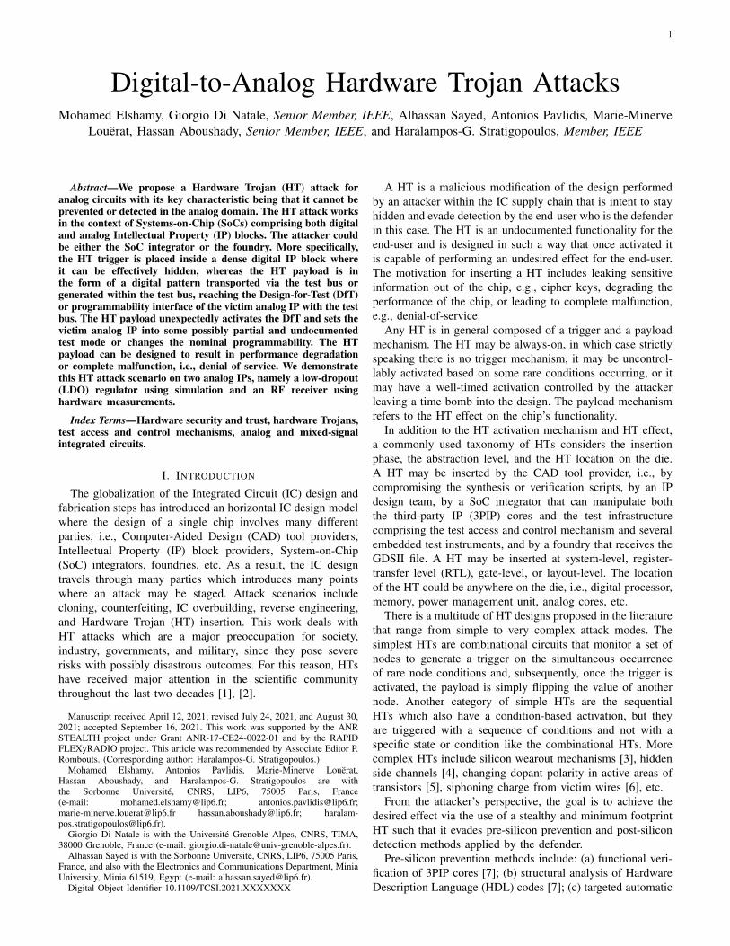
The LDO is one of the most popular power managementsystems to supply the sub-blocks of a SoC. It is a perfecttarget of a HT as the infection will spread to other IPs insidethe SoC. We designed an LDO in the 65nm technology bySTMicroelectronics using the free open-source OCEANE tool[82]. Its block-level schematic is shown in Fig. 6. It consists ofa sub-band gap reference voltage generator (SBGR), an erroramplifier implemented with an operational transconductanceamplifier (OTA), a power p-MOS transistor, and a feedback
8
Fig. 6: Block-level schematic of the LDO.
Fig. 7: Schematic of the error amplifier within the LDO implementedwith an OTA.
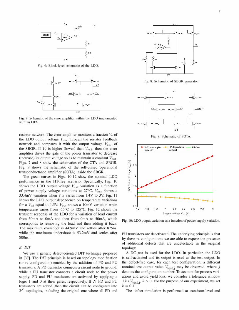
resistor network. The error amplifier monitors a fraction Ve ofthe LDO output voltage Vout through the resistor feedbacknetwork and compares it with the output voltage Vref ofthe SBGR. If Ve is higher (lower) than Vref , then the erroramplifier drives the gate of the power transistor to decrease(increase) its output voltage so as to maintain a constant Vout.Figs. 7 and 8 show the schematics of the OTA and SBGR.Fig. 9 shows the schematic of the self-biased operationaltransconductance amplifier (SOTA) inside the SBGR.
The green curves in Figs. 10-12 show the nominal LDOperformance in the HT-free scenario. Specifically, Fig. 10shows the LDO output voltage Vout variation as a functionof power supply voltage variations at 27oC. Vout shows a33.4mV variation when Vdd varies from 1.4V to 3V. Fig. 11shows the LDO output dependence on temperature variationsfor a Vdd equal to 1.5V. Vout shows a 10mV variation whentemperature varies from -55oC to 125oC. Fig. 12 shows thetransient response of the LDO for a variation of load currentfrom 50mA to 0mA and then from 0mA to 50mA, whichcorresponds to removing the load and then adding it back.The maximum overshoot is 44.9mV and settles after 875ns,while the maximum undershoot is 53.2mV and settles after800ns.
B. DfT
We use a generic defect-oriented DfT technique proposedin [37]. The DfT principle is based on topology modification(or re-configuration) enabled by the addition of PD and PUtransistors. A PD transistor connects a circuit node to ground,while a PU transistor connects a circuit node to the powersupply. PD and PU transistors are activated by applying alogic 1 and 0 at their gates, respectively. If N PD and PUtransistors are added, then the circuit can be configured into2N topologies, including the original one where all PD and
Fig. 8: Schematic of SBGR generator.
Fig. 9: Schematic of SOTA.
Fig. 10: LDO output variation as a function of power supply variation.
PU transistors are deactivated. The underlying principle is thatby these re-configurations we are able to expose the presenceof additional defects that are undetectable in the originaltopology.
A DC test is used for the LDO. In particular, the LDOis self-activated and its output is used as the test output. Inthe defect-free case, for each test configuration, a differentnominal test output value Vtest,j may be observed, where jdenotes the configuration number. To account for process vari-ations and avoid yield loss, we consider a tolerance window±k ∗Vtest,j, k > 0. For the purpose of our experiment, we setk = 0.1.
The defect simulation is performed at transistor-level and

9
Fig. 11: LDO output variation as a function of temperature variation.
Fig. 12: Transient response of the LDO for a variation of load current.
in an automated workflow using the Tessent®DefectSim toolby Mentor®, A Siemens Business [83]. We cycle through allconfigurations and for each configuration defects are injectedone by one. If Vtest,j is outside the tolerance window then thedefect is deemed detectable by the test configuration.
We use the default defect model of the tool [83]. Inparticular, for MOS transistors we use only gate open anddrain-to-source short defects. Similarly, for bipolar transistors,we consider base open and collector-emitter short defects. Weconsider the default short resistance of 10 ohms. Regardingopens, a weak pull-up or pull-down is assigned to each opendefect to account for the facts that an ideal open does notexist and, besides, it cannot be handled by a SPICE simulator[83]. For passive elements, i.e., resistors and capacitors, weconsider ±50% variations. In total, the defect model contains60 defects. Furthermore, any of the N added PU or PDtransistors could also contain defects, which increases thenumber of defects by 2N . We consider the absolute defectcoverage defined as the percentage of detected defects.
A defect coverage of 80% is reached using only the originaltopology. We applied the DfT technique considering that in a
given re-configuration only one PU or PD transistor can beenabled. The LDO has 14 nodes in total, thus the number ofpossible re-configurations is 28. We performed an exhaustivesearch and we identified several nodes where PD and PUtransistors can be added to result in a defect coverage of100%. We kept a minimum set of 3 PD/PU transistors toreduce the DfT overhead at a minimum while maintainingthe 100% defect coverage. The complete LDO schematic withthe embedded DfT infrastructure composed of the 3 PU/PDtransistors is shown in Fig. 13. One PD and one PU transistor,labelled by B1 and B2, respectively, are used inside the erroramplifier, and one PD transistor, labeled by B3, is used insidethe SBGR. The HT exploits this DfT infrastructure to stage theattack. The DfT is disabled with the pattern [B1,B2,B3]=010,while the patterns for enabling the three test configurations are[B1,B2,B3]=110, [B1,B2,B3]=000, and [B1,B2,B3]=011.
C. HT payload designAn interesting aspect of this DfT approach is that the DfT
interface inside the LDO, i.e., transistors B1, B2, and B3,has a digital word input and can be connected directly to thescan network without using a DAC. Another interesting aspectspecific to the LDO is that the LDO is self-driven withoutneeding to specify an analog test input.
The HT payload consists in applying a malicious DfTpattern during normal operation. We identified two such DfTpatterns that result in degradation of the LDO performanceand to complete malfunction, respectively.
In particular, applying the DfT pattern [B1,B2,B3]=110results in shifting the LDO output by about 15% and alsoresults in small variation of the LDO output for temperatureand Vdd variations, as shown by the orange curves in Figs.10-12. In more detail, enabling B1 results in zero gate voltagefor transistors MP O1 and MP O2 which increases the currentflowing through them. However, the sum of the currents staysfixed since it equals the current flowing through MN O3 whichis fixed. As the voltages of all terminals of MP O1 are fixed,it turns out that the current through MP O2 reduces, whichis enabled by the increase of the drain voltage of MP O2.This voltage drives the gate of the power p-MOS transistorMPS and, thereby, the current that flows through MPS reduces,which reduces the LDO output. In turn, this reduces thevoltage on the +Ve terminal which points to reduction of thesource voltage of MN O1 since the current flowing throughMP O1 is fixed. This feedback effect reduces the drain voltageof MN O2 which is the gate voltage of MPS. In the end, asit can be seen from Figs. 10-12, the LDO output settles at aslightly lower value of around 1V.
Applying the DfT pattern [B1,B2,B3]=011 results in acatastrophic effect in the operation of the LDO, as shown bythe red curves in Figs. 10-12. In more detail, setting B3=1connects the +Ve in terminal of the SOTA to ground. Theresult is that Vref follows Vdd instead of being stabilized at0.7V. Since the output of the LDO follows Vref , it shows alinear relationship with Vdd acting like a non-stabilized powersupply. In addition, once the load is removed the responseovershoots and never settles back unless the load is addedagain.

10
Fig. 13: LDO with DfT. The added PD and PU transistors to enable topology modifications are shown in red color.
Fig. 14: Highly-digitized RF receiver architecture.
VIII. CASE STUDY: RF RECEIVER
A. RF receiver programmable architecture
Our second case study is a programmable highly-digitizedmulti-standard RF receiver whose high-level architecture isillustrated in Fig. 14. A band-pass RF Σ∆ ADC is usedto directly convert the RF signal at the output of the lownoise amplifier (LNA) to the digital domain. The signal isthen down-converted by a digital mixer and filtered using adigital decimation filter. The RF receiver is designed with pro-grammable sub-blocks such that it can serve for establishingcommunication using several standards within the frequencyrange from 1.7 GHz to 2.8 GHz, including Bluetooth, ZigBee,WiFi 802.11b, etc. The programming aims at meeting thespecifications of the target standard, i.e., sensitivity, centerfrequency, bandwidth, and resolution, while at the same timecompensating for process variations and non-idealities so as toimprove the overall performance trade-off. The designer usesa complex calibration algorithm to find appropriate program-ming settings that are unique per standard and per chip. Theprogrammability is enabled by judiciously inserting digitally-controlled tuning knobs into the different sub-blocks.
The calibration is performed following testing/tuning it-erations towards optimising the performance trade-off. Theprogramming setting visited in each iteration is driven to theprogrammability interface via the scan network. For a givenchip, once the calibration has been completed, the final matrixof the programming setting per standard is stored in an on-chip memory. During the application, when the programmingsetting is to be updated, the new programming setting is calledfrom the associated memory address and driven to the RFreceiver via the scan network where it is latched into theregister of the programmability interface.
In our example, we infect the RF receiver via the modulatorof the Σ∆ ADC. We rely on a recent design in the 65nmtechnology by STMicroelectronics [59] whose block-levelarchitecture is illustrated in Fig. 15. The functionality of the
modulator is adjusted using a 194-bit programming word.Fig. 15 shows the number of bits of the programming wordcontrolling the operation of each sub-block.
Our experiment is conducted using hardware measurementson the actual fabricated chip. Without loss of generality, weconsider that the RF receiver operates with center frequency2.77GHz. The four main performances are plotted in Figs.16, 17, 18, and 19. The green curves correspond to thenominal HT-free operation. More specifically, Fig. 16 showsthe power spectral density (PSD) for an input power of -14dBm. The modulator has a nominal signal-to-noise ratio(SNR) of 60dB. Fig. 17 shows the SNR at different inputpower values with a step of 1dBm defining the dynamicrange (DR) of the modulator. Fig. 18 shows the spurious-freedynamic range (SFDR) measured by applying two tones at theinput with the same power and frequency difference of 2MHz.The modulator has a nominal SFDR of 51.39dB. Finally,Fig. 19 shows the output fundamental power and the third-order intermodulation (IM) product versus the input power,from which the input third-order intercept point (IP3) can bedetermined. The modulator has a nominal IP3 of 8dB.
B. HT payload design
The HT payload consists in unexpectedly altering the pro-gramming setting during normal operation. The issue hereis that the final programming settings per operation modeand per chip are defined during testing time, while the HTis planted at an earlier phase. In other words, the matrixof final programming settings is unknown to the attackerand, in any case, will change from one chip to another. Theattacker can still attain a controllable HT effect. The reasonis that the programming setting is divided into segments eachcontrolling a different sub-block, as shown in Fig. 15. Eachsegment of the programming setting can have one of tworoles, namely either calibrating against process variations orsetting the desired operation mode. Thus, for the HT to causecomplete malfunction it suffices that it randomly flips bitsin segments of the programming setting that are used forsetting the operation mode. Accordingly, for the HT to causeperformance degradation, it suffices that it randomly flipsbits in segments of the programming setting that are used tocalibrate against process variations. In fact, as we demonstratebelow, in both scenarios it suffices that the HT flips just onebit in the nominal programming setting, which facilitates theHT payload design.

11
Fig. 15: Architecture of Σ∆ modulator.
Fig. 16: PSD under HT-free and HT-infected operation.
Fig. 17: Dynamic range under HT-free and HT-infected operation.
Returning to our case study, a candidate block where theHT can act to incite performance degradation is the negativetransconductance -Gm in LC tank 1. The programmability of-Gm is responsible for improving the quality factor of the LCfilter. Flipping one single bit in the programmability of -Gmwill inevitably decrease the quality factor, thus untuning theRF receiver performance and degrading the SNR. The orangecurves in Figs. 16-19 show the HT-infected performances inthis scenario. As it can be seen, all performances are degraded.
A candidate block where the HT can act to incite completemalfunction is the tunable delay block in the feedback loop.The tunable delay block is responsible for controlling thecenter frequency of the noise shaping. It consists of delay
Fig. 18: SFDR under HT-free and HT-infected operation.
Fig. 19: IP3 under HT-free and HT-infected operation.
elements and the programming connects or disconnects themso as to control the delay time. Flipping one bit in itsprogrammming will inevitably set the RF receiver in anotheroperation mode, most likely in an undocumented and invalidoperation mode, thus leading to complete malfunction. Thered curves in Figs. 16-19 show the HT-infected performancesin this scenario. As it can be seen, there is no noise shapingand the signal now is buried under the noise floor.
IX. CONCLUSIONS
We proposed a novel HT attack scenario targeting infectinganalog IPs embedded in a SoC. The HT lies in the dense

12
digital circuitry and transports its payload to the victim analogIP via the test bus. The payload consists of a malicious DfTpattern or programmability setting and is applied to the analogIP via the DfT circuitry or programmability fabric that areaccessed via the test bus. We proposed different designs ofthe HT payload mechanism, while any HT trigger mechanismcan be used in this context. The proposed HT attack wasdemonstrated on two case studies, namely an LDO regulatorand an RF receiver. In the LDO case study, we considered aneffective DfT approach and we derived malicious DfT patternsthat can lead to performance degradation or denial-of-service.In the RF receiver case study, we demonstrated with hardwaremeasurements that the infection can succeed by flipping onlya select bit in the programming of the ADC that digitizes thereceived signal. The key characteristic of the proposed HTattack is that it is totally invisible in the analog domain, whileit is stealthy and has a small footprint since the HT mechanismis hidden in its entirety into the digital part of the SoC.
REFERENCES
[1] S. Bhunia, M. S. Hsiao, M. Banga, and S. Narasimhan, “Hardwaretrojan attacks: Threat analysis and countermeasures,” Proceedings ofthe IEEE, vol. 102, no. 8, pp. 1229–1247, 2014.
[2] K. Xiao, D. Forte, Y. Jin, R. Karri, S. Bhunia, and M. Tehranipoor,“Hardware Trojans: lessons learned after one decade of research,” ACMTransactions on Design Automation of Electronic Systems, vol. 22, no.1, pp. 6:1–6:23, 2016.
[3] Y. Shiyanovskii, F. Wolff, A. Rajendran, C. Papachristou, D. Weyer,and W. Clay, “Process reliability based trojans through NBTI and HCIeffects,” in NASA/ESA Conference on Adaptive Hardware and Systems,2010, pp. 215–222.
[4] L. Lin, T. Guneysu M. Kasper, C. Paar, and W. Burleson, “Trojanside-channels: Lightweight hardware trojans through side-channel engi-neering,” in Cryptographic Hardware and Embedded Systems - CHES2009. 2009, pp. 382–395, Springer Berlin Heidelberg.
[5] G. T. Becker, F. Regazzoni, C. Paar, and W. P. Burleson, “Stealthydopant-level hardware trojans: Extended version,” Journal of Crypto-graphic Engineering, vol. 4, no. 1, pp. 19–31, 2014.
[6] K. Yang, M. Hicks, Q. Dong, T. Austin, and D. Sylvester, “A2: analogmalicious hardware,” in Proc. IEEE Symposium on Security and Privacy,2016, pp. 18–37.
[7] X. Zhang and M. Tehranipoor, “Case study: Detecting hardware trojansin third-party digital IP cores,” in IEEE International Symposium onHardware-Oriented Security and Trust, 2011, pp. 67–70.
[8] R. S. Chakraborty, F. Wolff, S. Paul, C. Papachristou, and S. Bhunia,“MERO: A statistical approach for hardware trojan detection,” inCryptographic Hardware and Embedded Systems - CHES 2009. 2009,pp. 396–410, Springer Berlin Heidelberg.
[9] V. R. Surabhi, P. Krishnamurthy, H. Amrouch, K. Basu, J. Henkel,R. Karri, and F. Khorrami, “Hardware trojan detection using controlledcircuit aging,” IEEE Access, vol. 8, pp. 77415–77434, 2020.
[10] V. R. Surabhi, P. Krishnamurthy, H. Amrouch, J. Henkel, R. Karri, andF. Khorrami, “Exposing hardware trojans in embedded platforms viashort-term aging,” IEEE Transactions on Computer-Aided Design ofIntegrated Circuits and Systems, vol. 39, no. 11, pp. 3519–3530, 2020.
[11] M. Hicks, M. Finnicum, S. T. King, M. M. K. Martin, and J. M. Smith,“Overcoming an untrusted computing base: Detecting and removingmalicious hardware automatically,” in IEEE Symposium on Securityand Privacy, 2010, pp. 159–172.
[12] K. Xiao, D. Forte, and M. Tehranipoor, “A novel built-in self-authentication technique to prevent inserting hardware trojans,” IEEETransactions on Computer-Aided Design of Integrated Circuits andSystems, vol. 33, no. 12, pp. 1778–1791, 2014.
[13] J. Leonhard, M. Yasin, S. Turk, M. Nabeel, M.-M. Louerat,R. Chotin-Avot, H. Aboushady, O. Sinanoglu, and H.-G. Stratigopoulos,“MixLock: Securing mixed-signal circuits via logic locking,” in Proc.Design, Automation & Test in Europe Conference, 2019.
[14] N. Limaye, E. Kalligeros, N. Karousos, I. G. Karybali, and O. Sinanoglu,“Thwarting all logic locking attacks: Dishonest oracle with truly randomlogic locking,” IEEE Transactions on Computer-Aided Design ofIntegrated Circuits and Systems, vol. 40, no. 9, pp. 1740–1753, 2021.
[15] J. Rajendran, M. Sam, O. Sinanoglu, and R. Karri, “Security analysis ofintegrated circuit camouflaging,” in Proc. ACM Conference on Computerand Communications Security, 2013, pp. 709–720.
[16] J. Leonhard, A. Sayed, M. Louerat, H. Aboushady, and H. Stratigopou-los, “Analog and mixed-signal IC security via sizing camouflaging,”IEEE Transactions on Computer-Aided Design of Integrated Circuitsand Systems, vol. 40, no. 5, pp. 822–835, 2021.
[17] T. D. Perez and S. Pagliarini, “A survey on split manufacturing: Attacks,defenses, and challenges,” IEEE Access, vol. 8, pp. 184013–184035,2020.
[18] T. Sugawara, D. Suzuki, R. Fujii, S. Tawa, R. Hori, M. Shiozaki,and T. Fujino, “Reversing stealthy dopant-level circuits,” Journal ofCryptographic Engineering, vol. 5, no. 2, pp. 85–94, 2015.
[19] B. Lippmann, M. Werner, N. Unverricht, A. Singla, P. Egger,A. Dubotzky, H. Gieser, M. Rasche, O. Kellermann, and H. Graeb,“Integrated flow for reverse engineering of nanoscale technologies,” inProc. Asia and South Pacific Design Automation Conference, 2019, p.82–89.
[20] F. Stellari, P. Song, A. J. Weger, J. Culp, A. Herbert, and D. Pfeiffer,“Verification of untrusted chips using trusted layout and emission mea-surements,” in IEEE International Symposium on Hardware-OrientedSecurity and Trust, 2014, pp. 19–24.
[21] D. Agrawal, S. Baktir, D. Karakoyunlu, P. Rohatgi, and B. Sunar,“Trojan detection using IC fingerprinting,” in IEEE Symposium onSecurity and Privacy, 2007, pp. 296–310.
[22] Y. Jin and Y. Makris, “Hardware trojan detection using path delayfingerprint,” in IEEE International Workshop on Hardware-OrientedSecurity and Trust, 2008, pp. 51–57.
[23] S. Narasimhan, W. Yueh, X. Wang, S. Mukhopadhyay, and S. Bhunia,“Improving IC security against trojan attacks through integration ofsecurity monitors,” IEEE Design & Test of Computers, vol. 29, no.5, pp. 37–46, 2012.
[24] D. Forte, C. Bao, and A. Srivastava, “Temperature tracking: An inno-vative run-time approach for hardware trojan detection,” in IEEE/ACMInternational Conference on Computer-Aided Design, 2013, pp. 532–539.
[25] B. Shakya, T. He, H. Salmani, D. Forte, S. Bhunia, and M. Tehranipoor,“Benchmarking of hardware trojans and maliciously affected circuits,”Journal of Hardware and Systems Security, vol. 1, no. 1, pp. 85–102,2017.
[26] Y. Jin and Y. Makris, “Hardware trojans in wireless cryptographic ICs,”IEEE Design & Test of Computers, vol. 27, no. 1, pp. 26–35, 2010.
[27] Y. Liu, Y. Jin, A. Nosratinia, and Y. Makris, “Silicon demonstrationof hardware trojan design and detection in wireless cryptographic ICs,”IEEE Transactions on Very Large Scale Integration (VLSI) Systems, vol.25, no. 4, pp. 1506–1519, 2017.
[28] S. Chang, G. Bhat, U. Ogras, B. Bakkaloglu, and S. Ozev, “Detectionmechanisms for unauthorized wireless transmissions,” ACM Transac-tions on Design Automation of Electronic Systems, vol. 23, no. 6, pp.70:1–70:21, 2018.
[29] K. S. Subramani, N. Helal, A. Antonopoulos, A. Nosratinia, andY. Makris, “Amplitude-modulating analog/RF hardware trojans in wire-less networks: Risks and remedies,” IEEE Transactions on InformationForensics and Security, vol. 15, pp. 3497–3510, 2020.
[30] Z. Liu, Y. Li, Y. Duan, R. L. Geiger, and D. Chen, “Identification andbreak of positive feedback loops in trojan states vulnerable circuits,” inProc. IEEE International Symposium on Circuits and Systems, 2014, pp.289–292.
[31] X. Cao, Q. Wang, R. L. Geiger, and D. J. Chen, “A hardware trojanembedded in the inverse widlar reference generator,” in Proc. IEEEInternational Midwest Symposium on Circuits and Systems, 2015.
[32] Q. Wang, R. L. Geiger, and D. Chen, “Hardware trojans embedded inthe dynamic operation of analog and mixed-signal circuits,” in Proc.National Aerospace and Electronics Conference, 2015, pp. 155–158.
[33] C. Cai and D. Chen, “Performance enhancement induced trojan statesin op-amps, their detection and removal,” in Proc. IEEE InternationalSymposium on Circuits and Systems, 2015, pp. 3020–3023.
[34] Q. Wang, D. Chen, and R. L. Geiger, “Transparent side channel triggermechanism on analog circuits with PAAST hardware trojans,” in IEEEInternational Symposium on Circuits and Systems, 2018.
[35] M. Elshamy, G. Di Natale, A. Pavlidis, M. Louerat, and H. Stratigopou-los, “Hardware trojan attacks in analog/mixed-signal ICs via the testaccess mechanism,” in IEEE European Test Symposium, 2020.

13
[36] G. Huertas, D. Vazquez, E. J. Peralıas, A. Rueda, and J. L. Huertas,“Testing mixed-signal cores: A practical oscillation-based test in ananalog macrocell,” IEEE Design & Test of Computers, vol. 19, no.6, pp. 73–82, 2002.
[37] A. Coyette, B. Esen, W. Dobbelaere, R. Vanhooren, and G. Gielen, “Au-tomatic generation of test infrastructures for analog integrated circuitsby controllability and observability co-optimization,” Integration, theVLSI Journal, vol. 55, pp. 393–400, 2016.
[38] A. Pavlidis, M. M. Louerat, E. Faehn, A. Kumar, and H. G. Stratigopou-los, “SymBIST: Symmetry-based analog and mixed-signal built-in self-test for functional safety,” IEEE Transactions on Circuits and SystemsI: Regular Papers, vol. 68, no. 6, pp. 2580–2593, 2021.
[39] A. Chatterjee, “Concurrent error detection and fault-tolerance in linearanalog circuits using continuous checksums,” IEEE Transactions onVery Large Scale Integration (VLSI) Systems, vol. 1, no. 2, pp. 138–150, 1993.
[40] H.-G. D. Stratigopoulos and Y. Makris, “Concurrent detection oferroneous responses in linear analog circuits,” IEEE Transactions onComputer-Aided Design of Integrated Circuits and Systems, vol. 25, no.5, pp. 878–891, 2006.
[41] G. Renaud, M. Diallo, M. J. Barragan, and S. Mir, “Fully differential4-V output range 14.5-ENOB stepwise ramp stimulus generator for on-chip static linearity test of ADCs,” IEEE Transactions on Very LargeScale Integration (VLSI) Systems, vol. 27, no. 2, pp. 281–293, 2019.
[42] F. Azais, S. Bernard, Y. Bertrand, and M. Renovell, “Optimizingsinusoidal histogram test for low cost ADC BIST,” Journal of ElectronicTesting: Theory and Applications, vol. 17, no. 3-4, pp. 255–266, 2001.
[43] A. Laraba, H.-G. Stratigopoulos, S. Mir, and H. Naudet, “Exploitingpipeline ADC properties for a reduced-code linearity test technique,”IEEE Transactions on Circuits and Systems I: Regular Papers, vol. 62,no. 10, pp. 2391–2400, 2015.
[44] T. Chen, X. Jin, R. L. Geiger, and D. Chen, “USER-SMILE: Ultrafaststimulus error removal and segmented model identification of linearityerrors for ADC built-in self-test,” IEEE Transactions on Circuits andSystems I: Regular Papers, vol. 65, no. 7, pp. 2059–2069, 2018.
[45] B. Dufort and G. W. Roberts, “On-chip analog signal generation formixed-signal built-in self-test,” IEEE Journal of Solid-State Circuits,vol. 34, no. 3, pp. 318–30, 1999.
[46] H. Malloug, M. J. Barragan, and S. Mir, “Practical harmonic cancel-lation techniques for the on-chip implementation of sinusoidal signalgenerators for mixed-signal BIST applications,” Journal of ElectronicTesting: Theory and Applications, vol. 34, no. 3, pp. 263–279, 2018.
[47] M. Barragan, R. Alhakim, H.-G. Stratigopoulos, M. Dubois, S. Mir,H. Le Gall, N. Bhargava, and A. Bal, “A fully-digital BIST wrapperbased on ternary test stimuli for the dynamic test of a 40nm CMOS 18-bit stereo audio Σ∆ ADC,” IEEE Transactions on Circuits and SystemsI: Regular Papers, vol. 63, no. 11, pp. 1876–1888, 2016.
[48] H. Chauhan, Y. Choi, M. Onabajo, I.-S. Jung, and Y.-B. Kim, “Accurateand efficient on-chip spectral analysis for built-in testing and calibrationapproaches,” IEEE Transactions on Very Large Scale Integration (VLSI)Systems, vol. 22, no. 3, pp. 49 –506, 2014.
[49] S. Sunter and A. Roy, “On-chip digital jitter measurement, frommegahertz to gigahertz,” IEEE Design & Test of Computers, vol. 21,no. 4, pp. 314–321, 2004.
[50] H. Le-Gall, R. Alhakim, M. Valka, S. Mir, H. Stratigopoulos, andE. Simeu, “High frequency jitter estimator for SoCs,” in IEEE EuropeanTest Symposium, 2015.
[51] M. Ince, E. Yilmaz, W. Fu, J. Park, K. Nagaraj, L. Winemberg, andS. Ozev, “Digital built-in self-test for phased locked loops to enablefault detection,” in IEEE European Test Symposium, 2019.
[52] A. Valdes-Garcia, J. Silva-Martinez, and E. Sanchez-Sinencio, “On-chiptesting techniques for RF wireless transceivers,” IEEE Design & Testof Computers, vol. 23, no. 4, pp. 268–277, 2006.
[53] E. S. Erdogan and S. Ozev, “Detailed characterization of transceiverparameters through loop-back-based BiST,” IEEE Transactions on VeryLarge Scale Integration (VLSI) Systems, vol. 18, no. 6, pp. 901–911,2010.
[54] M. Cimino, H. Lapuyade, Y. Deval, T. Taris, and J.-B. Begueret, “Designof a 0.9V 2.45 GHz self-testable and reliability-enhanced CMOS LNA,”IEEE Journal of Solid-State Circuits, vol. 43, no. 5, pp. 1187–1194,2008.
[55] Y.-C. Huang, H.-H. Hsieh, and L.-H. Lu, “A built-in self-test techniquefor RF low-noise amplifiers,” IEEE Transactions on Microwave Theoryand Techniques, vol. 56, no. 2, pp. 1035–1042, 2008.
[56] L. Abdallah, H.-G. Stratigopoulos, S. Mir, and J. Altet, “Defect-orientednon-intrusive RF test using on-chip temperature sensors,” in Proc. IEEEVLSI Test Symposium, 2013.
[57] L. Abdallah, H.-G. Stratigopoulos, S. Mir, and C. Kelma, “Experienceswith non-intrusive sensors for RF built-in test,” in Proc. IEEE Interna-tional Test Conference, 2012, Paper 17.1.
[58] S. Li, J. Li, X. Gu, H. Wang, C. Li, J. Wu, and M. Tang, “ReconfigurableAll-Band RF CMOS Transceiver for GPS/GLONASS/Galileo/BeidouWith Digitally Assisted Calibration,” IEEE Transactions on Very LargeScale Integration (VLSI) Systems, vol. 23, no. 9, pp. 1814–1827, 2015.
[59] A. Sayed, T. Badran, M. Louerat, and H. Aboushady, “A 1.5-to-3.0GHztunable RF sigma-delta ADC with a fixed set of coefficients and aprogrammable loop delay,” IEEE Transactions on Circuits and SystemsII: Express Briefs, vol. 67, no. 9, pp. 1559–1563, 2020.
[60] M. Andraud, H.-G. Stratigopoulos, and E. Simeu, “One-shot non-intrusive calibration against process variations for analog/RF circuits,”IEEE Transactions on Circuits and Systems I: Regular Papers, vol. 63,no. 11, pp. 2022–2035, 2016.
[61] A. Antonopoulos, G. Volanis, Y. Lu, and Y. Makris, “Post-productioncalibration of analog/RF ICs: Recent developments and a fully integratedsolution,” in International Conference on Synthesis, Modeling, Analysisand Simulation Methods and Applications to Circuit Design, 2019, pp.77–80.
[62] C. Maxey, G. Creech, S. Raman, J. Rockway, K. Groves, T. Quach,L. Orlando, and A. Mattamana, “Mixed-signal SoCs with in situ self-healing circuitry,” IEEE Design & Test of Computers, vol. 29, no. 6,pp. 27–39, 2012.
[63] S. Lee, C. Shi, J. Wang, A. Sanabria, H. Osman, J. Hu, and E. Sanchez-Sinencio, “A built-in self-test and In Situ analog circuit optimizationplatform,” IEEE Transactions on Circuits and Systems I: Regular Papers,vol. 65, no. 10, pp. 3445–3458, 2018.
[64] S. Sunter, J.-F. Cote, and J. Rearick, “Streaming access to ADCs andDACs for mixed-signal ATPG,” IEEE Design & Test, vol. 33, no. 6, pp.38–45, 2016.
[65] M. Portolan, “Automated testing flow: The present and the future,”IEEE Transactions on Computer-Aided Design of Integrated Circuitsand Systems, vol. 39, no. 10, pp. 2952–2963, 2020.
[66] “IEEE standard for access and control of instrumentation embeddedwithin a semiconductor device,” IEEE Std 1687-2014, 2014.
[67] “IEEE standard for a mixed-signal test bus,” IEEE Std 1149.4-2010(Revision of IEEE Std 1149.4-1999), 2011.
[68] “IEEE standard for describing analog test access and control,https://standards.ieee.org/project/1687 2.html,” IEEE Std P1687.2.
[69] B. Yang, K. Wu, and R. Karri, “Secure scan: A design-for-testarchitecture for crypto chips,” IEEE Transactions on Computer-AidedDesign of Integrated Circuits and Systems, vol. 25, no. 10, pp. 2287–2293, 2006.
[70] J. Da Rolt, G. Di Natale, M. Flottes, and B. Rouzeyre, “New securitythreats against chips containing scan chain structures,” in IEEE Inter-national Symposium on Hardware-Oriented Security and Trust, 2011.
[71] L. Azriel, R. Ginosar, and A. Mendelson, “Revealing on-chip proprietarysecurity functions with scan side channel based reverse engineering,” inProc. Great Lakes Symposium on VLSI, 2017, p. 233–238.
[72] Ing. M.F. Breeuwsma, “Forensic imaging of embedded systems usingJTAG (boundary-scan),” Digital Investigation, vol. 3, no. 1, pp. 32–42,2006.
[73] F. Majeric, B. Gonzalvo, and L. Bossuet, “JTAG combined attack -another approach for fault injection,” in IFIP International Conferenceon New Technologies, Mobility and Security, 2016, pp. 1–5.
[74] K. Rosenfeld and R. Karri, “Attacks and defenses for JTAG,” IEEEDesign Test of Computers, vol. 27, no. 1, pp. 36–47, 2010.
[75] E. Valea, M. Da Silva, G. Di Natale, M.-L. Flottes, and B. Rouzeyre, “Asurvey on security threats and countermeasures in IEEE test standards,”IEEE Design & Test, vol. 36, no. 3, pp. 95–116, 2019.
[76] F. Novak and A. Biasizzo, “Security extension for IEEE std 1149.1.,”Journal of Electronic Testing, vol. 22, pp. 301–303, 2006.
[77] A. Das, J. D. Rolt, S. Ghosh, S. Seys, S. Dupuis, G. D. Natale,M.-L. Flottes, B. Rouzeyre, and I. Verbauwhede, “Secure JTAGimplementation using schnorr protocol,” Journal of Electronic Testing,vol. 29, pp. 193–209, 2013.
[78] R. Baranowski, M. A. Kochte, and H. Wunderlich, “Fine-grained accessmanagement in reconfigurable scan networks,” IEEE Transactions onComputer-Aided Design of Integrated Circuits and Systems, vol. 34, no.6, pp. 937–946, 2015.
[79] J. Dworak, A. Crouch, J. Potter, A. Zygmontowicz, and M. Thornton,“Don’t forget to lock your SIB: hiding instruments using P1687,” inIEEE International Test Conference, 2013.
[80] C. Clark, “Anti-tamper JTAG TAP design enables DRM to JTAG regis-ters and P1687 on-chip instruments,” in IEEE International Symposiumon Hardware-Oriented Security and Trust, 2010, pp. 19–24.

14
[81] S. Kan, J. Dworak, and J. G. Dunham, “Echeloned IJTAG dataprotection,” in IEEE Asian Hardware-Oriented Security and Trust, 2016.
[82] J. Porte, “Outil pour la conception et l’enseignementd’electronique analogique (OCEANE),” https://www-soc.lip6.fr/equipe-cian/logiciels/oceane/, Online.
[83] S. Sunter, K. Jurga, and A. Laidler, “Using mixed-signal defectsimulation to close the loop between design and test,” IEEE Transactionson Circuits and Systems I: Regular Papers, vol. 63, no. 12, pp. 2313–2322, 2016.
Mohamed Elshamy received the M.Sc. degree inElectronics and Communications Engineering fromCairo University, Giza, Egypt, in 2015 and the Ph.Ddegree from Sorbonne Universite, Paris, France, in2021. He is currently a research assistant in the lab-oratory of nanotechnology application in electronicsat the Electronics Research Institute, Cairo, Egypt.His research interests include hardware security,analog and mixed-signal circuits, nano-electronics,and memristors.
Giorgio Di Natale (Senior Member, IEEE) receivedthe PhD in Computer Engineering from the Politec-nico di Torino in 2003. He works as Director ofResearch for the French National Research Center(CNRS), and he is the director of the TIMA lab-oratory in Grenoble. His research interests includehardware security and trust, secure circuits designand test, reliability evaluation and fault tolerance,software implemented hardware fault tolerance, andVLSI testing. He serves as chair of the IEEE Com-puter Society TTTC from 2020, he is Golden Core
member of the Computer Society and Senior member of the IEEE.
Alhassan Sayed received the B.Sc. and the M.Sc.degrees in Electrical Engineering, from the Electron-ics and Communications Department, Minia Uni-versity, Minia, Egypt, in 2007 and 2010, respec-tively. He obtained his Ph.D. degree in ElectricalEngineering and Computer Science from SorbonneUniversity, Paris, France, in 2016. He also spent 2years (2017-2019) in a postdoctoral research posi-tion at the same University. Dr. Sayed is currentlyan Assistant Professor at Minia University, Minia,Egypt. His research interests include Sigma-Delta
modulation, analog and RF circuit design, Analog-to-Digital conversion, andlow noise amplifiers.
Antonios Pavlidis received the Diploma in elec-trical and computer engineering from the AristotleUniversity of Thessaloniki, Thessaloniki, Greece,in 2017, and the Ph.D. degree from the SorbonneUniversite, Paris, France, in 2021. He is currentlya Post-doctoral Researcher with the Laboratoired’Informatique de Paris 6 (LIP6) at Sorbonne Uni-versite. His research interests include analog andmixed signal (AMS) circuits testing, Built-in-self-test (BIST) and Design-for-Test (DfT) for AMScircuits, fault diagnosis techniques for AMS circuits,
Analog-to-Digital Converters (ADCs), machine learning, and hardware secu-rity.
Marie-Minerve Louerat received the M.Sc. degreein Electrical Engineering and the Ph.D. degree fromUniversite Paris Sud, Orsay, France, in 1983 and1986 respectively. In 1986 she joined the Centre Na-tional de la Recherche Scientifique (CNRS), France.She started at Fluids, Automation and ThermalSystems Laboratory, Universite Paris Sud-CNRS,while teaching electronics. In 1992, she moved tothe Computer Science Laboratory (LIP6), UniversityPierre et Marie Curie (now Sorbonne Universite)-CNRS, France, while teaching VLSI. Between 2013
and 2018, she was the head of the System on Chip Department at LIP6. Dr.Louerat’s research interest is electronic design automation methods and toolsfor analogue and mixed-signal circuits and systems. Most of her researchactivities have been supported by contracts, through academic and industrialcooperative projects in the framework of the FP7, Eureka/MEDEA, Catrene,Penta, and H2020 Projects. She published papers on static timing analysis,analogue and AMS design automation, analogue-to-digital converters, AMSsystem modelling and simulation, and test and security of AMS circuits andsystems. She is a member of the AMS Working Group of Accellera SystemsInitiative and contributed to standardize the AMS extension of SystemCsince 2010. She has served on the Technical Program Committee of Design,Automation, and Test in European Conference (DATE) and several othersinternational conferences. She co-chaired the Free Silicon Conference (FSIC)in 2019, Paris, France.
Hassan Aboushady (Senior Member, IEEE) re-ceived the B.Sc. degree in Electrical Engineer-ing from Cairo University, Egypt, in 1993, theM.Sc. and Ph.D. degrees in Electrical Engineeringand Computer Science from Sorbonne University,Paris, France, in 1996 and 2002 respectively. Dr.Aboushady is currently an Associate Professor atSorbonne University. His research interests includeSigma-Delta modulation, Analog/RF circuit design,Analog-to-Digital and Digital-to-Analog conversion,as well as Security in analog and mixed-signal
circuits. He is the author and co-author of more than 70 publications in theseareas. He is the recipient of the 2004 best paper award in the IEEE DesignAutomation and Test in Europe Conference, as well as the recipient and theco-recipient of the 2nd and the 3rd best student paper awards of the IEEEMidwest Symposium on Circuits and Systems in 2000 and 2003 respectively.Dr. Aboushady is an IEEE-CAS distinguished lecturer and a member of theIEEE Circuits and Systems for Communications Committee (CASCOM). Healso served as an Associate Editor of the IEEE Transactions on Circuits andSystems II: Express Briefs.
Haralampos-G. Stratigopoulos (Member, IEEE)received the Diploma in electrical and computerengineering from the National Technical Universityof Athens, Athens, Greece, in 2001 and the Ph.D.in electrical engineering from Yale University, NewHaven, USA, in 2006. He is a Research Direc-tor with the French National Center for ScientificResearch (CNRS) at LIP6 Laboratory, SorbonneUniversite, Paris, France. His main research interestsare in the areas of design-for-test for analog, mixed-signal, RF circuits and systems, machine learning,
hardware security, and neuromorphic computing. He was the General Chairof the 2015 IEEE International Mixed-Signal Testing Workshop (IMSTW) andthe Program Chair of the 2017 IEEE European Test Symposium (ETS). He hasserved on the Technical Program Committees of Design, Automation, and Testin Europe Conference (DATE), Design Automation Conference (DAC), IEEEInternational Conference on Computer-Aided Design (ICCAD), IEEE Euro-pean Test Symposium (ETS), IEEE International Test Conference (ITC), IEEEVLSI Test Symposium (VTS), and several others international conferences. Hehas served as an Associate Editor of IEEE Transactions on Computer-AidedDesign of Integrated Circuits and Systems, IEEE Transactions on Circuitsand Systems I: Regular Papers, IEEE Design & Test, and Springer Journal ofElectronic Testing: Theory & Applications. He received the Best Paper Awardin the 2009, 2012, and 2015 IEEE European Test Symposium (ETS).
Related Documents