TMS320C203, TMS320C209, TMS320LC203 DIGITAL SIGNAL PROCESSORS SPRS025B – JUNE 1995 – REVISED AUGUST 1998 1 POST OFFICE BOX 1443 • HOUSTON, TEXAS 77251–1443 Based Upon the T320C2xLP Core CPU 16-Bit Fixed-Point DSP Architecture – Six Internal Buses for Increased Parallelism and Performance – 32-Bit ALU/Accumulator – 16 × 16-Bit Single-Cycle Multiplier With a 32-Bit Product – Block Moves for Data, Program, I/O Space – Hardware Repeat Instruction Instruction Cycle Time ’C203 ’LC203 ’C209 50 ns @ 5 V 50 ns @ 3.3 V 50 ns @ 5 V 35 ns @ 5 V 35 ns @ 5 V 25 ns @ 5 V Source Code Compatible With TMS320C25 Upwardly Code-Compatible With TMS320C5x Devices Four External Interrupts Boot-Loader Option (’C203 Only) TMS320C2xx Integrated Memory: – 544 × 16 Words of On-Chip Dual-Access Data RAM – 4K × 16 Words of On-Chip Single-Access Program/Data RAM (’C209 only) – 4K × 16 Words of On-Chip Program ROM (’C209 Only) 224K × 16-Bit Total Addressable External Memory Space – 64K Program – 64K Data – 64K I/O – 32K Global TMS320C2xx Peripherals: – PLL With Various Clock Options – ×1, ×2, ×4, 2 (’C203) – ×2, 2 (’C209) – On-Chip Oscillator – One Wait State Software-Programmable to Each Space (’C209 Only) – 0 – 7 Wait States Software-Programmable to Each Space (’C203 Only) – Six General-Purpose I/O Pins – On-Chip 20-Bit Timer – Full-Duplex Asynchronous Serial Port (UART) (’C203 Only) – One Synchronous Serial Port With Four-Level-Deep FIFOs (’C203 Only) Supports Hardware Wait States Designed for Low-Power Consumption – Fully Static CMOS Technology – Power-Down IDLE Mode 1.1 mA/MIPS at 3.3 V ’C203 is Pin-Compatible With TMS320F206 Flash DSP Up to 40-MIPS Performance at 5 V (’C203) 20-MIPS Performance at 3.3 V HOLD Mode for Multiprocessor Applications IEEE-1149.1 ² -Compatible Scan-Based Emulation 80- and 100-pin Small Thin Quad Flat Packages (TQFPs), (PN and PZ Suffixes) description The TMS320C2xx generation of digital signal processors (DSPs) combines strong performance and great flexibility to meet the needs of signal processing and control applications. The T320C2xLP core CPU that is the basis of all ’C2xx devices has been optimized for high speed, small size, and low-power, making it ideal for demanding applications in many markets. The CPU has an advanced, modified Harvard architecture with six internal buses that permits tremendous parallelism and data throughput. The powerful ’C2xx instruction set makes software development easy. And because the ’C2xx is code-compatible with the TMS320C2x and ’C5x generations, your code investment is preserved. Around this core, ’C2xx-generation devices feature various combinations of on-chip memory and peripherals. The serial ports provide easy communication with external devices such as codecs, A/D converters, and other processors. Other peripherals that facilitate the control of external devices include general-purpose I/O pins, a 20-bit timer, and a wait-state generator. Please be aware that an important notice concerning availability, standard warranty, and use in critical applications of Texas Instruments semiconductor products and disclaimers thereto appears at the end of this data sheet. PRODUCTION DATA information is current as of publication date. Products conform to specifications per the terms of Texas Instruments standard warranty. Production processing does not necessarily include testing of all parameters. Copyright 1998, Texas Instruments Incorporated ² IEEE Standard 1149.1-1990, IEEE Standard Test-Access Port.

Welcome message from author
This document is posted to help you gain knowledge. Please leave a comment to let me know what you think about it! Share it to your friends and learn new things together.
Transcript

TMS320C203, TMS320C209, TMS320LC203DIGITAL SIGNAL PROCESSORS
SPRS025B – JUNE 1995 – REVISED AUGUST 1998
1POST OFFICE BOX 1443 • HOUSTON, TEXAS 77251–1443
Based Upon the T320C2xLP Core CPU
16-Bit Fixed-Point DSP Architecture– Six Internal Buses for Increased
Parallelism and Performance– 32-Bit ALU/Accumulator– 16 × 16-Bit Single-Cycle Multiplier With a
32-Bit Product– Block Moves for Data, Program,
I/O Space– Hardware Repeat Instruction
Instruction Cycle Time’C203 ’LC203 ’C20950 ns @ 5 V 50 ns @ 3.3 V 50 ns @ 5 V35 ns @ 5 V 35 ns @ 5 V25 ns @ 5 V
Source Code Compatible With TMS320C25
Upwardly Code-Compatible WithTMS320C5x Devices
Four External Interrupts
Boot-Loader Option (’C203 Only)
TMS320C2xx Integrated Memory:– 544 × 16 Words of On-Chip Dual-Access
Data RAM– 4K × 16 Words of On-Chip Single-Access
Program/Data RAM (’C209 only)– 4K × 16 Words of On-Chip Program ROM
(’C209 Only)
224K × 16-Bit Total Addressable ExternalMemory Space– 64K Program– 64K Data– 64K I/O– 32K Global
TMS320C2xx Peripherals:– PLL With Various Clock Options
– ×1, ×2, ×4, 2 (’C203)– ×2, 2 (’C209)
– On-Chip Oscillator– One Wait State Software-Programmable
to Each Space (’C209 Only)– 0 – 7 Wait States Software-Programmable
to Each Space (’C203 Only)– Six General-Purpose I/O Pins– On-Chip 20-Bit Timer– Full-Duplex Asynchronous Serial Port
(UART) (’C203 Only)– One Synchronous Serial Port With
Four-Level-Deep FIFOs (’C203 Only)
Supports Hardware Wait States
Designed for Low-Power Consumption– Fully Static CMOS Technology– Power-Down IDLE Mode
1.1 mA/MIPS at 3.3 V
’C203 is Pin-Compatible With TMS320F206Flash DSP
Up to 40-MIPS Performance at 5 V (’C203)
20-MIPS Performance at 3.3 V
HOLD Mode for MultiprocessorApplications
IEEE-1149.1†-Compatible Scan-BasedEmulation
80- and 100-pin Small Thin Quad FlatPackages (TQFPs), (PN and PZ Suffixes)
description
The TMS320C2xx generation of digital signal processors (DSPs) combines strong performance and greatflexibility to meet the needs of signal processing and control applications. The T320C2xLP core CPU that is thebasis of all ’C2xx devices has been optimized for high speed, small size, and low-power, making it ideal fordemanding applications in many markets. The CPU has an advanced, modified Harvard architecture with sixinternal buses that permits tremendous parallelism and data throughput. The powerful ’C2xx instruction setmakes software development easy. And because the ’C2xx is code-compatible with the TMS320C2x and ’C5xgenerations, your code investment is preserved. Around this core, ’C2xx-generation devices feature variouscombinations of on-chip memory and peripherals. The serial ports provide easy communication with externaldevices such as codecs, A/D converters, and other processors. Other peripherals that facilitate the control ofexternal devices include general-purpose I/O pins, a 20-bit timer, and a wait-state generator.
Please be aware that an important notice concerning availability, standard warranty, and use in critical applications ofTexas Instruments semiconductor products and disclaimers thereto appears at the end of this data sheet.
PRODUCTION DATA information is current as of publication date.Products conform to specifications per the terms of Texas Instrumentsstandard warranty. Production processing does not necessarily includetesting of all parameters.
Copyright 1998, Texas Instruments Incorporated
† IEEE Standard 1149.1-1990, IEEE Standard Test-Access Port.

TMS320C203, TMS320C209, TMS320LC203DIGITAL SIGNAL PROCESSORS
SPRS025B – JUNE 1995 – REVISED AUGUST 1998
2 POST OFFICE BOX 1443 • HOUSTON, TEXAS 77251–1443
description (continued)
Because of their strong performance, low cost, and easy-to-use development environment, ’C2xx-generationDSPs are an ideal choice for applications such as smart phones, digital cameras, modems, remote metering,and security systems.
HO
LD/I
NT
1
RSBIOXFIO1IO0RX
VSS
TXTOUT
VDD
DXFSXVSS
CLKXDR
FSRCLKR
VSS
TDOTMS
TDITRST
TCKEMU1/OFF
EMU0
D3D4D5D6VSS
D7D8D9D10VDD
D11VSS
D12D13D14D15VSS
BRWERDSTRBR/WVSS
READYVDD50
494847464544434241403938373635343332313029282726100
999897969594939291908988878685848382818079787776
25242322212019181716151413121110987654321
51525354555657585960616263646566676869707172737475
V A15
A14
A13
A12
V A11
A10
A9
A8
V A7
V A6
A5
A4
V A3
A2
A1
A0
V PS
IS DSS
S
DD
SS
SS
SS
DD
TE
ST
BO
OT
DIV
1V D
IV2
HO
LDA
VIO
2IO
3P
LL5V
VC
LKIN
/X2
X1
VC
LKO
UT
1V N
MI
INT
2IN
T3
V D0
D1
D2
VDD
DD
DD SS
DD SS
SS
PZ PACKAGE(TOP VIEW)
CLK
IN/X
2
RS
MP/MCD15VSSD14D13VDDD12D11D10D9D8
EMU0EMU1/OFF
1234567891011121314151617181920
6162636465666768697071727374757677787980
6059585756555453525150494847464544434241
4039383736353433323130292827262524232221T
RS
TIA
CK
RD
V XF
CLK
MO
DV T
OU
T
X1
BR
PS
IS DS
WE
V
SS
SS
D7
D6
D5
D4
D3
SS
D1
TM
SIN
T1
INT
2IN
T3
NM
I
PLL
5V A0
A12
CLK
OU
T1
R/W
RA
ME
N
PN PACKAGE(TOP VIEW)
ST
RB
TD
O
A4
D2
D0
RE
S1
VDD
RSTDI
READYTCKBIO
A15A14A13
VSSA11A10A9A8VDDVDDA7A6VSSA5
A3
A2A1VSS
DD
SS
SS
V V V
Table 2 provides a comparison of the devices in the ’C2xx generation. It shows the capacity of on-chip RAMand ROM, the number of serial and parallel I/O ports, the execution time of one machine cycle, and the typeof package with total pin count.
Table 1. Low Power Dissipation †
POWER TMS320C203 TMS320C209
3.3 V 1.1 mA/MIPS N/A
5 V 1.9 mA/MIPS 1.9 mA/MIPS† Core power dissipation. For complete details, see Calculation of TMS320C2xx Power Dissipation (literature
number SPRA088).
Table 2. Characteristics of the TMS320C2xx Processors
ON-CHIP MEMORYI/O PORTS POWER CYCLE PACKAGE
TMS320C2xx RAM ROMI/O PORTS POWER
SUPPLYCYCLETIME
PACKAGETYPE WITH
DEVICESDATA
DATA/PROG PROG SERIAL PARALLEL
SUPPLY(V)
TIME(ns)
TYPE WITHPIN COUNT
TMS320C203 288 256 – 2 64K 5 50/35/25 100-pin TQFP
TMS320C209 288 4K + 256 4K – 64K 5 50/35 80-pin TQFP
TM320LC203 288 256 – 2 64K 3.3 50 100-pin TQFP

TMS320C203, TMS320C209, TMS320LC203DIGITAL SIGNAL PROCESSORS
SPRS025B – JUNE 1995 – REVISED AUGUST 1998
3POST OFFICE BOX 1443 • HOUSTON, TEXAS 77251–1443
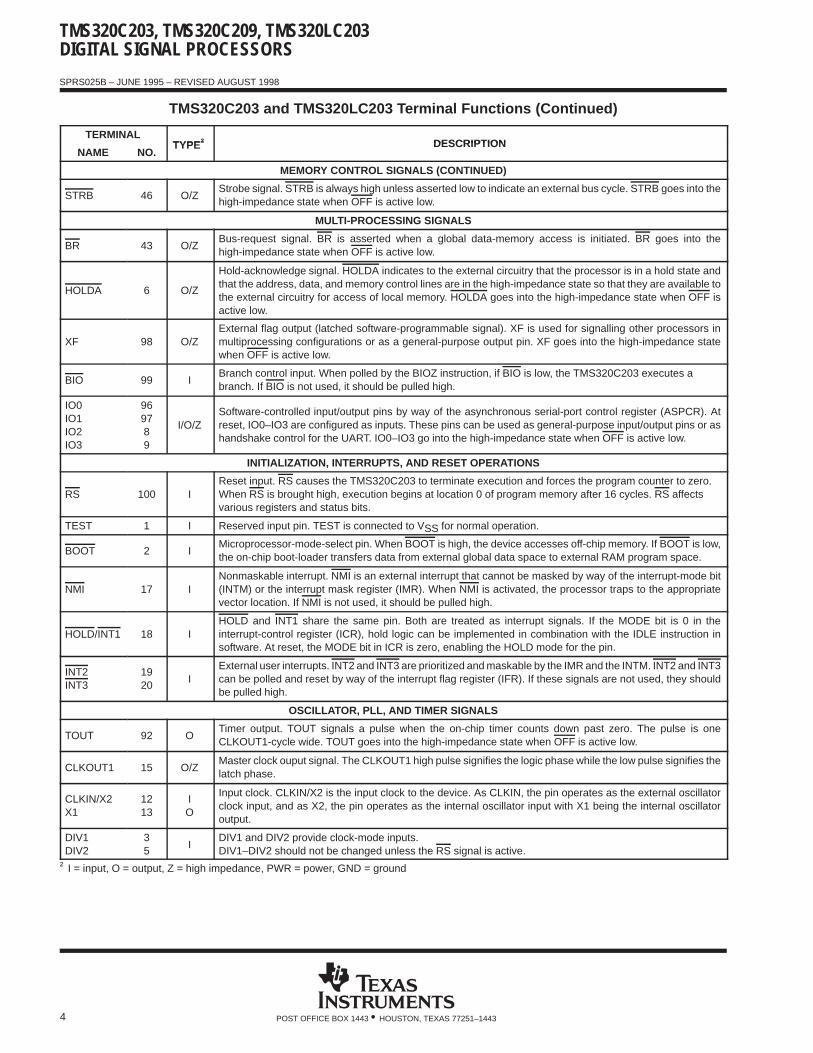
TMS320C203 and TMS320LC203 Terminal Functions
TERMINALTYPE† DESCRIPTION
NAME NO. TYPE† DESCRIPTION
DATA AND ADDRESS BUSES
D15D14D13D12D11D10D9D8D7D6D5D4D3D2D1D0
41403938363433323129282726242322
I/O/Z
Parallel data bus D15 [most significant bit (MSB)] through D0 [least significant bit (LSB)]. D15–D0 aremultiplexed to transfer data between the TMS320C2xx and external data/program memory or I/Odevices. Placed in the high-impedance state when not outputting (R/W high) or RS when asserted. Theygo into the high-impedance state when OFF is active low.
A15A14A13A12A11A10A9A8A7A6A5A4A3A2A1A0
74737271696867666462616058575655
O/Z
Parallel address bus A15 (MSB) through A0 (LSB). A15–A0 are multiplexed to address externaldata/program memory or I/O devices. These signals go into the high-impedance state when OFF is activelow.
MEMORY CONTROL SIGNALS
PS 53 O/ZProgram-select signal. PS is always high unless low-level asserted for communicating to off-chip programspace. PS goes into the high-impedance state when OFF is active low.
DS 51 O/ZData-select signal. DS is always high unless low-level asserted for communicating to off-chip programspace. DS goes into the high-impedance state when OFF is active low.
IS 52 O/ZI/O space-select signal. IS is always high unless low-level asserted for communicating to I/O ports. ISgoes into the high-impedance state when OFF is active low.
READY 49 IData-ready input. READY indicates that an external device is prepared for the bus transaction to becompleted. If the external device is not ready (READY low), the TMS320C203 waits one cycle and checksREADY again. If READY is not used, it should be pulled high.
R/W 47 O/ZRead/write signal. R/W indicates transfer direction when communicating to an external device. R/W isnormally in read mode (high), unless low level is asserted for performing a write operation. R/W goes intothe high-impedance state when OFF is active low.
RD 45 O/ZRead-select indicates an active, external read cycle and can connect directly to the output enable (OE)of external devices. RD is active on all external program, data, and I/O reads. RD goes into thehigh-impedance state when OFF is active low.
WE 44 O/ZWrite enable. The falling edge of WE indicates that the device is driving the external data bus (D15–D0).Data can be latched by an external device on the rising edge of WE. WE is active on all external program,data, and I/O writes. WE goes into the high-impedance state when OFF is active low.
† I = input, O = output, Z = high impedance, PWR = power, GND = ground
TMS320C203, TMS320C209, TMS320LC203DIGITAL SIGNAL PROCESSORS
SPRS025B – JUNE 1995 – REVISED AUGUST 1998
4 POST OFFICE BOX 1443 • HOUSTON, TEXAS 77251–1443
TMS320C203 and TMS320LC203 Terminal Functions (Continued)
TERMINALTYPE† DESCRIPTION
NAME NO.TYPE† DESCRIPTION
MEMORY CONTROL SIGNALS (CONTINUED)
STRB 46 O/ZStrobe signal. STRB is always high unless asserted low to indicate an external bus cycle. STRB goes into thehigh-impedance state when OFF is active low.
MULTI-PROCESSING SIGNALS
BR 43 O/ZBus-request signal. BR is asserted when a global data-memory access is initiated. BR goes into thehigh-impedance state when OFF is active low.
HOLDA 6 O/Z
Hold-acknowledge signal. HOLDA indicates to the external circuitry that the processor is in a hold state andthat the address, data, and memory control lines are in the high-impedance state so that they are available tothe external circuitry for access of local memory. HOLDA goes into the high-impedance state when OFF isactive low.
XF 98 O/ZExternal flag output (latched software-programmable signal). XF is used for signalling other processors inmultiprocessing configurations or as a general-purpose output pin. XF goes into the high-impedance statewhen OFF is active low.
BIO 99 IBranch control input. When polled by the BIOZ instruction, if BIO is low, the TMS320C203 executes abranch. If BIO is not used, it should be pulled high.
IO0IO1IO2IO3
969789
I/O/ZSoftware-controlled input/output pins by way of the asynchronous serial-port control register (ASPCR). Atreset, IO0–IO3 are configured as inputs. These pins can be used as general-purpose input/output pins or ashandshake control for the UART. IO0–IO3 go into the high-impedance state when OFF is active low.
INITIALIZATION, INTERRUPTS, AND RESET OPERATIONS
RS 100 IReset input. RS causes the TMS320C203 to terminate execution and forces the program counter to zero.When RS is brought high, execution begins at location 0 of program memory after 16 cycles. RS affectsvarious registers and status bits.
TEST 1 I Reserved input pin. TEST is connected to VSS for normal operation.
BOOT 2 IMicroprocessor-mode-select pin. When BOOT is high, the device accesses off-chip memory. If BOOT is low,the on-chip boot-loader transfers data from external global data space to external RAM program space.
NMI 17 INonmaskable interrupt. NMI is an external interrupt that cannot be masked by way of the interrupt-mode bit(INTM) or the interrupt mask register (IMR). When NMI is activated, the processor traps to the appropriatevector location. If NMI is not used, it should be pulled high.
HOLD/INT1 18 IHOLD and INT1 share the same pin. Both are treated as interrupt signals. If the MODE bit is 0 in theinterrupt-control register (ICR), hold logic can be implemented in combination with the IDLE instruction insoftware. At reset, the MODE bit in ICR is zero, enabling the HOLD mode for the pin.
INT2INT3
1920
IExternal user interrupts. INT2 and INT3 are prioritized and maskable by the IMR and the INTM. INT2 and INT3can be polled and reset by way of the interrupt flag register (IFR). If these signals are not used, they shouldbe pulled high.
OSCILLATOR, PLL, AND TIMER SIGNALS
TOUT 92 OTimer output. TOUT signals a pulse when the on-chip timer counts down past zero. The pulse is oneCLKOUT1-cycle wide. TOUT goes into the high-impedance state when OFF is active low.
CLKOUT1 15 O/ZMaster clock ouput signal. The CLKOUT1 high pulse signifies the logic phase while the low pulse signifies thelatch phase.
CLKIN/X2X1
1213
IO
Input clock. CLKIN/X2 is the input clock to the device. As CLKIN, the pin operates as the external oscillatorclock input, and as X2, the pin operates as the internal oscillator input with X1 being the internal oscillatoroutput.
DIV1DIV2
35
IDIV1 and DIV2 provide clock-mode inputs.DIV1–DIV2 should not be changed unless the RS signal is active.
† I = input, O = output, Z = high impedance, PWR = power, GND = ground

TMS320C203, TMS320C209, TMS320LC203DIGITAL SIGNAL PROCESSORS
SPRS025B – JUNE 1995 – REVISED AUGUST 1998
5POST OFFICE BOX 1443 • HOUSTON, TEXAS 77251–1443
TMS320C203 and TMS320LC203 Terminal Functions (Continued)
TERMINALTYPE† DESCRIPTION
NAME NO.TYPE† DESCRIPTION
OSCILLATOR, PLL, AND TIMER SIGNALS (CONTINUED)
PLL5V 10 IPLL operating at 5 V. When the device is operating at 5 V, PLL5V should be tied high. When the device isoperating at 3.3 V, PLL5V should be tied low.
SERIAL PORT AND UART SIGNALS
CLKX 87 I/O
Transmit clock. CLKX is a clock signal for clocking data from the transmit shift register (XSR) to the DXdata-transmit pin. The CLKX can be an input if the MCM bit in the synchronous serial-port control register(SSPCR) is set to 0. CLKX can also be driven by the device at one-half of the CLKOUT1 frequency whenMCM = 1. If the serial port is not being used, CLKX goes into the high-impedance state when OFF is activelow. Value at reset is as an input.
CLKR 84 I/OReceive-clock input. External clock signal for clocking data from the DR (data-receive) pin into the serial-portreceive shift register (RSR). CLKR must be present during serial-port transfers. If the serial port is not beingused, CLKR can be sampled as an input by the IN0 bit of the SSPCR.
FSR 85 I/OFrame synchronization pulse for receive input. The falling edge of the FSR pulse initiates the data-receiveprocess, beginning the clocking of the RSR. FSR goes into the high-impedance state when OFF is active low.
FSX 89 I/O
Frame synchronization pulse for transmit input/ouput. The falling edge of the FSX pulse initiates thedata-transmit process, beginning the clocking of the serial-port transmit shift register (XSR). Following reset,FSX is an input. FSX can be selected by software to be an output when the TXM bit in the SSPCR is set to1. FSX goes into the high-impedance state when OFF is active low.
DR 86 I Serial-data receive input. Serial data is received in the receive shift register (RSR) through the DR pin.
DX 90 OSerial-port transmit output. Serial data is transmitted from the transmit shift register (XSR) through the DX pin.DX is in the high-impedance state when OFF is active low.
TX 93 O Asynchronous transmit pin
RX 95 I Asynchronous receive pin
TEST SIGNALS
TRST 79 I
IEEE Standard 1149.1 (JTAG) test reset. TRST, when active high, gives the scan system control of theoperations of the device. If TRST is not connected or driven low, the device operates in its functional mode,and the test signals are ignored.If the TRST pin is not driven, an external pulldown resistor must be used.
TCK 78 I
JTAG test clock. TCK is normally a free-running clock signal with a 50% duty cycle. The changes on thetest-access port (TAP) input signals (TMS and TDI) are clocked into the TAP controller, instruction register, orselected test-data register on the rising edge of TCK. Changes at the TAP output signal (TDO) occur on thefalling edge of TCK.
TMS 81 I JTAG test-mode select. TMS is clocked into the TAP controller on the rising edge of TCK.
TDI 80 I JTAG test-data input. TDI is clocked into the selected register (instruction or data) on a rising edge of TCK.
TDO 82 O/ZJTAG test-data output. The contents of the selected register (instruction or data) are shifted out of TDO on thefalling edge of TCK. TDO is in the high-impedance state except when the scanning of data is in progress.
EMU0 76 I/O/ZEmulator pin 0. When TRST is driven low, EMU0 must be high for activation of the OFF condition. When TRSTis driven high, EMU0 is used as an interrupt to or from the emulator system and is defined as an input/outputthrough the JTAG scan.
EMU1/OFF 77 I/O/Z
Emulator pin 1. Emulator pin 1 disables all outputs. When TRST is driven high, EMU1/OFF is used as aninterrupt to or from the emulator system and is defined as an input/output through the JTAG scan. When TRSTis driven low, this pin is configured as OFF. EMU1/OFF, when active low, puts all output drivers in thehigh-impedance state. Note that OFF is used exclusively for testing and emulation purposes (not formultiprocessing applications). Therefore, for the OFF condition, the following apply:TRST = 0EMU0 = 1EMU/OFF = 0
† I = input, O = output, Z = high impedance, PWR = power, GND = ground

TMS320C203, TMS320C209, TMS320LC203DIGITAL SIGNAL PROCESSORS
SPRS025B – JUNE 1995 – REVISED AUGUST 1998
6 POST OFFICE BOX 1443 • HOUSTON, TEXAS 77251–1443
TMS320C203 and TMS320LC203 Terminal Functions (Continued)
TERMINALTYPE† DESCRIPTION
NAME NO.TYPE† DESCRIPTION
SUPPLY PINS
VDD
4711163550637591
PWR Power
VSS
1421253037424854596570838894
GND Ground
† I = input, O = output, Z = high impedance, PWR = power, GND = ground
TMS320C203, TMS320C209, TMS320LC203DIGITAL SIGNAL PROCESSORS
SPRS025B – JUNE 1995 – REVISED AUGUST 1998
7POST OFFICE BOX 1443 • HOUSTON, TEXAS 77251–1443
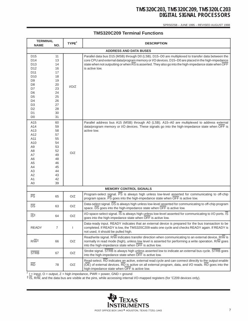
TMS320C209 Terminal Functions
TERMINALTYPE† DESCRIPTION
NAME NO. TYPE† DESCRIPTION
ADDRESS AND DATA BUSES
D15D14D13D12D11D10D9D8D7D6D5D4D3D2D1D0
11131416171819202324252627283031
I/O/Z
Parallel data bus D15 (MSB) through D0 (LSB). D15–D0 are multiplexed to transfer data between thecore CPU and external data/program memory or I/O devices. D15–D0 are placed in the high-impedancestate when not outputting or when RS is asserted. They also go into the high-impedance state when OFFis active low.
A15A14A13A12A11A10A9A8A7A6A5A4A3A2A1A0
60595857555453524948464544434239
O/Z
Parallel address bus A15 (MSB) through A0 (LSB). A15–A0 are multiplexed to address externaldata/program memory or I/O devices. These signals go into the high-impedance state when OFF isactive low.
MEMORY CONTROL SIGNALS
PS 65 O/ZProgram-select signal. PS is always high unless low-level asserted for communicating to off-chipprogram space. PS goes into the high-impedance state when OFF is active low.
DS 63 O/ZData-select signal. DS is always high unless low-level asserted for communicating to off-chip programspace. DS goes into the high-impedance state when OFF is active low.
IS‡ 64 O/ZI/O-space-select signal. IS is always high unless low-level asserted for communicating to I/O ports. ISgoes into the high-impedance state when OFF is active low.
READY 7 IData-ready input. READY indicates that an external device is prepared for the bus transaction to becompleted. If READY is low, the TMS320C209 waits one cycle and checks READY again. If READY isnot used, it should be pulled high.
R/W‡ 66 O/ZRead/write signal. R/W indicates transfer direction when communicating to an external device. R/W isnormally in read mode (high), unless low level is asserted for performing a write operation. R/W goesinto the high-impedance state when OFF is active low.
STRB 67 O/ZStrobe signal. STRB is always high unless asserted low to indicate an external bus cycle. STRB goesinto the high-impedance state when OFF is active low.
RD 78 O/ZRead-select. RD indicates an active, external read cycle and can connect directly to the output enable(OE) of external devices. RD is active on all external program, data, and I/O reads. RD goes into thehigh-impedance state when OFF is active low.
† I = input, O = output, Z = high impedance, PWR = power, GND = ground‡ IS, R/W, and the data bus are visible at the pins, while accessing internal I/O-mapped registers (for ’C209 devices only).
TMS320C203, TMS320C209, TMS320LC203DIGITAL SIGNAL PROCESSORS
SPRS025B – JUNE 1995 – REVISED AUGUST 1998
8 POST OFFICE BOX 1443 • HOUSTON, TEXAS 77251–1443
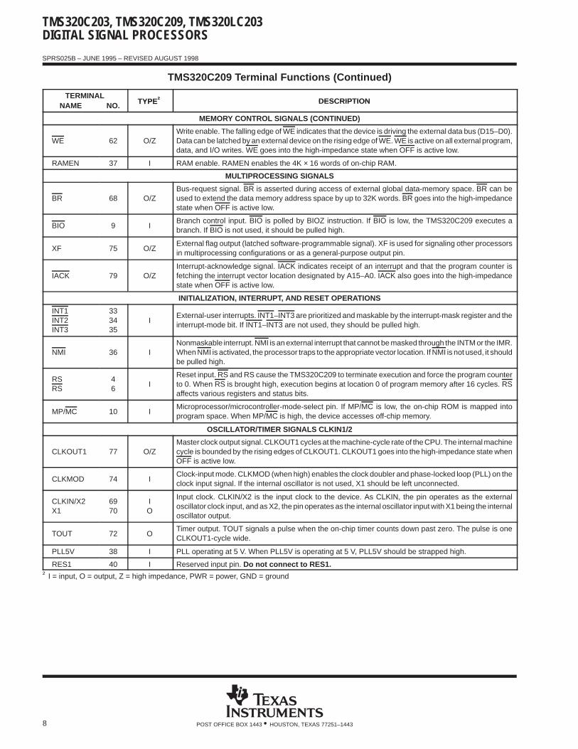
TMS320C209 Terminal Functions (Continued)
TERMINALTYPE† DESCRIPTION
NAME NO. TYPE† DESCRIPTION
MEMORY CONTROL SIGNALS (CONTINUED)
WE 62 O/ZWrite enable. The falling edge of WE indicates that the device is driving the external data bus (D15–D0).Data can be latched by an external device on the rising edge of WE. WE is active on all external program,data, and I/O writes. WE goes into the high-impedance state when OFF is active low.
RAMEN 37 I RAM enable. RAMEN enables the 4K × 16 words of on-chip RAM.
MULTIPROCESSING SIGNALS
BR 68 O/ZBus-request signal. BR is asserted during access of external global data-memory space. BR can beused to extend the data memory address space by up to 32K words. BR goes into the high-impedancestate when OFF is active low.
BIO 9 IBranch control input. BIO is polled by BIOZ instruction. If BIO is low, the TMS320C209 executes abranch. If BIO is not used, it should be pulled high.
XF 75 O/ZExternal flag output (latched software-programmable signal). XF is used for signaling other processorsin multiprocessing configurations or as a general-purpose output pin.
IACK 79 O/ZInterrupt-acknowledge signal. IACK indicates receipt of an interrupt and that the program counter isfetching the interrupt vector location designated by A15–A0. IACK also goes into the high-impedancestate when OFF is active low.
INITIALIZATION, INTERRUPT, AND RESET OPERATIONS
INT1INT2INT3
333435
IExternal-user interrupts. INT1–INT3 are prioritized and maskable by the interrupt-mask register and theinterrupt-mode bit. If INT1–INT3 are not used, they should be pulled high.
NMI 36 INonmaskable interrupt. NMI is an external interrupt that cannot be masked through the INTM or the IMR.When NMI is activated, the processor traps to the appropriate vector location. If NMI is not used, it shouldbe pulled high.
RSRS
46
IReset input. RS and RS cause the TMS320C209 to terminate execution and force the program counterto 0. When RS is brought high, execution begins at location 0 of program memory after 16 cycles. RSaffects various registers and status bits.
MP/MC 10 IMicroprocessor/microcontroller-mode-select pin. If MP/MC is low, the on-chip ROM is mapped intoprogram space. When MP/MC is high, the device accesses off-chip memory.
OSCILLATOR/TIMER SIGNALS CLKIN1/2
CLKOUT1 77 O/ZMaster clock output signal. CLKOUT1 cycles at the machine-cycle rate of the CPU. The internal machinecycle is bounded by the rising edges of CLKOUT1. CLKOUT1 goes into the high-impedance state whenOFF is active low.
CLKMOD 74 IClock-input mode. CLKMOD (when high) enables the clock doubler and phase-locked loop (PLL) on theclock input signal. If the internal oscillator is not used, X1 should be left unconnected.
CLKIN/X2X1
6970
IO
Input clock. CLKIN/X2 is the input clock to the device. As CLKIN, the pin operates as the externaloscillator clock input, and as X2, the pin operates as the internal oscillator input with X1 being the internaloscillator output.
TOUT 72 OTimer output. TOUT signals a pulse when the on-chip timer counts down past zero. The pulse is oneCLKOUT1-cycle wide.
PLL5V 38 I PLL operating at 5 V. When PLL5V is operating at 5 V, PLL5V should be strapped high.
RES1 40 I Reserved input pin. Do not connect to RES1.† I = input, O = output, Z = high impedance, PWR = power, GND = ground
TMS320C203, TMS320C209, TMS320LC203DIGITAL SIGNAL PROCESSORS
SPRS025B – JUNE 1995 – REVISED AUGUST 1998
9POST OFFICE BOX 1443 • HOUSTON, TEXAS 77251–1443
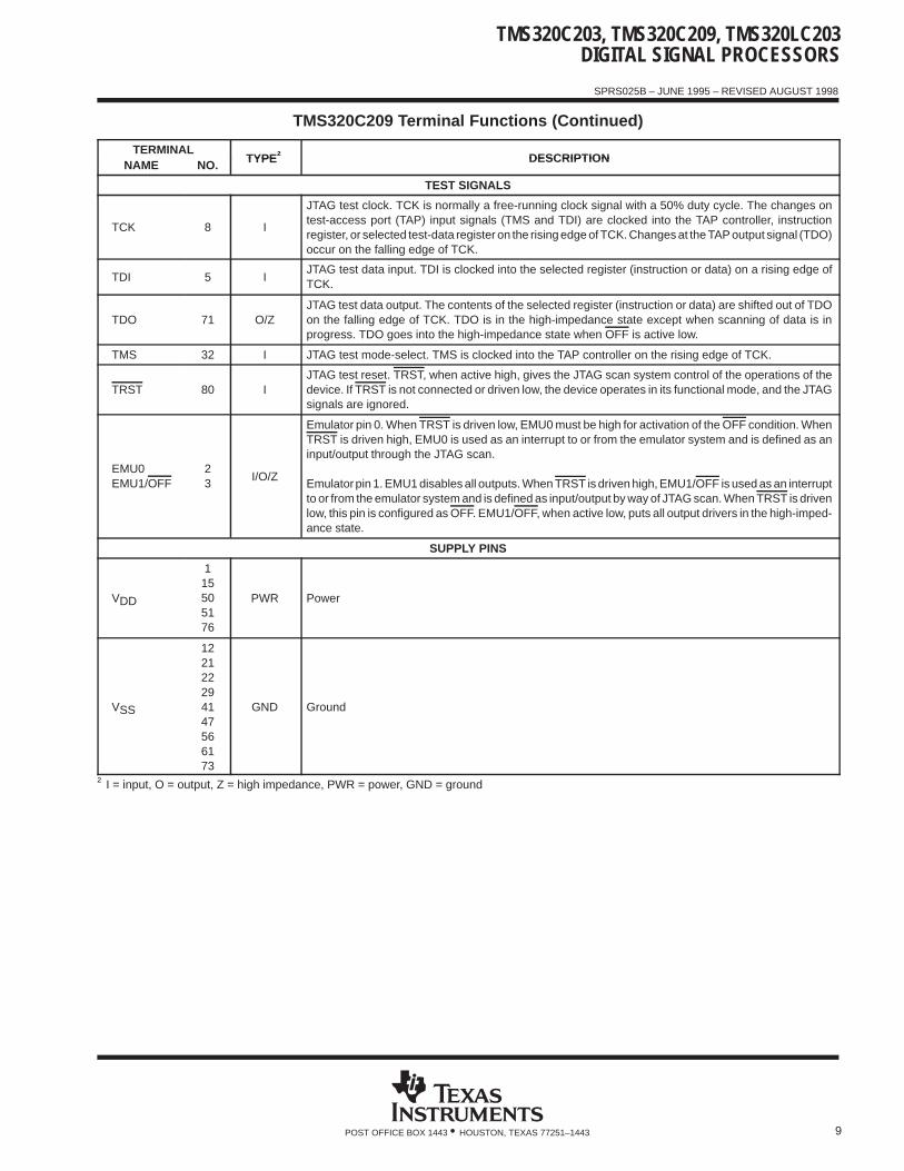
TMS320C209 Terminal Functions (Continued)
TERMINALTYPE† DESCRIPTION
NAME NO. TYPE† DESCRIPTION
TEST SIGNALS
TCK 8 I
JTAG test clock. TCK is normally a free-running clock signal with a 50% duty cycle. The changes ontest-access port (TAP) input signals (TMS and TDI) are clocked into the TAP controller, instructionregister, or selected test-data register on the rising edge of TCK. Changes at the TAP output signal (TDO)occur on the falling edge of TCK.
TDI 5 IJTAG test data input. TDI is clocked into the selected register (instruction or data) on a rising edge ofTCK.
TDO 71 O/ZJTAG test data output. The contents of the selected register (instruction or data) are shifted out of TDOon the falling edge of TCK. TDO is in the high-impedance state except when scanning of data is inprogress. TDO goes into the high-impedance state when OFF is active low.
TMS 32 I JTAG test mode-select. TMS is clocked into the TAP controller on the rising edge of TCK.
TRST 80 IJTAG test reset. TRST, when active high, gives the JTAG scan system control of the operations of thedevice. If TRST is not connected or driven low, the device operates in its functional mode, and the JTAGsignals are ignored.
EMU0EMU1/OFF
23
I/O/Z
Emulator pin 0. When TRST is driven low, EMU0 must be high for activation of the OFF condition. WhenTRST is driven high, EMU0 is used as an interrupt to or from the emulator system and is defined as aninput/output through the JTAG scan.
Emulator pin 1. EMU1 disables all outputs. When TRST is driven high, EMU1/OFF is used as an interruptto or from the emulator system and is defined as input/output by way of JTAG scan. When TRST is drivenlow, this pin is configured as OFF. EMU1/OFF, when active low, puts all output drivers in the high-imped-ance state.
SUPPLY PINS
VDD
115505176
PWR Power
VSS
122122294147566173
GND Ground
† I = input, O = output, Z = high impedance, PWR = power, GND = ground

TMS320C203, TMS320C209, TMS320LC203DIGITAL SIGNAL PROCESSORS
SPRS025B – JUNE 1995 – REVISED AUGUST 1998
10 POST OFFICE BOX 1443 • HOUSTON, TEXAS 77251–1443
functional block diagram of the ’C2xx internal hardware
TCR
Timer
32
16
Data Bus
16
16
OSCALE (0–7)
D15–D0
A15–A0
16
1616
32
32
ACCL(16)ACCH(16)C
32
CALU(32)
3232
MUX
ISCALE (0–16)
16
MUX
PREG(32)
Multiplier
TREG0(16)
MUX
16
1616
MUX
B1 (256x16)
B2 (32x16)DARAM
B0 (256x16)DARAM
MUX
7LSBfromIR
MUX
DP(9)
9
9
MUX
16
SARAM†
16
ARAU(16)
16
MUX
3
3
3
3
ARB(3)
ARP(3)
Program Bus
16
16
16
16
AR7(16)
AR6(16)
AR5(16)
AR3(16)
AR2(16)
AR1(16)
AR0(16)
Address
Instruction
Stack 8 x16
PC
MUX
NMIWERD
16
CLKIN/X2CLKOUT1X1
3INT[3:1]
BOOT/MP/MC
RS
HOLDA†HOLD†
XFBR
READYSTRB
R/W
PSDSIS
DIV2DIV1
Con
trol
Dat
a B
us
Pro
gram
Bus
Dat
a B
us
AR4(16)
16
MU
XM
UX
Data/Prog
Data/Prog
16
PSCALE (–6,0,1,4)
16
Data
32
16
16
16
16
16
ROM/FLASH†
MUX
MUX
NPAR
PAR MSTACK
Program Control(PCTRL)
PRD
TIM
ADTR
ASP†
SSPCR
SSP†
SDTR
4
TOUT
TX
RX
I/O PINS
DXCLKX
FSXDR
FSRCLKR
BRD
IOSR
Reserved
Memory MapRegister
IMR (16)
IFR (16)
GREG (16)
16
Pro
gram
Bus
I/O-Mapped Registers
† Not available on all devices (see Table 2).NOTES: A. Symbol descriptions appear in Table 3.
B. For clarity, the data and program buses are shown as single buses although they include address and data bits.

TMS320C203, TMS320C209, TMS320LC203DIGITAL SIGNAL PROCESSORS
SPRS025B – JUNE 1995 – REVISED AUGUST 1998
11POST OFFICE BOX 1443 • HOUSTON, TEXAS 77251–1443
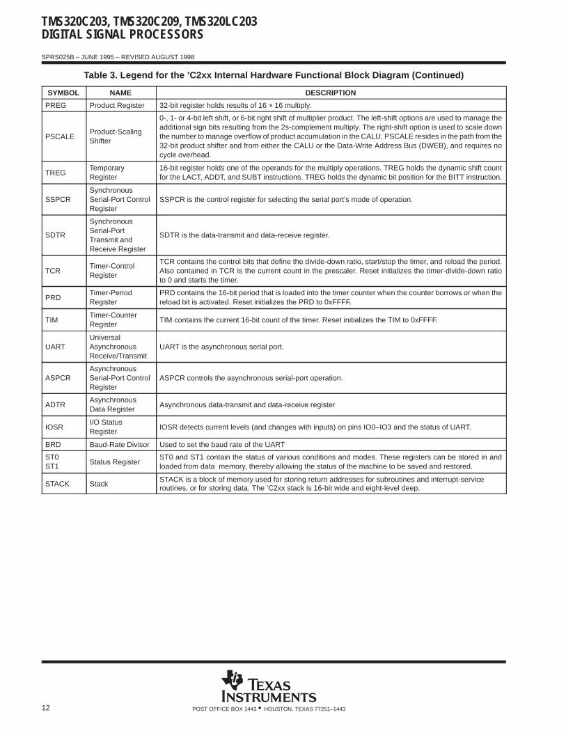
Table 3. Legend for the ’C2xx Internal Hardware Functional Block Diagram
SYMBOL NAME DESCRIPTION
ACC Accumulator32-bit register that stores the results and provides input for subsequent CALU operations. Also includesshift and rotate capabilities
ARAUAuxiliary RegisterArithmetic Unit
An unsigned, 16-bit arithmetic unit used to calculate indirect addresses using the auxiliary registers asinputs and outputs
AUXREGS
Auxiliary Registers0–7
These 16-bit registers are used as pointers to anywhere within the data space address range. They areoperated upon by the ARAU and are selected by the auxiliary register pointer (ARP). AR0 can also be usedas an index value for AR updates of more than one and as a compare value to AR.
BR Bus Register SignalBR is asserted during access of the external global data memory space. READY is asserted to the devicewhen the global data memory is available for the bus transaction. BR can be used to extend the datamemory address space by up to 32K words.
C CarryRegister carry output from CALU. C is fed back into the CALU for extended arithmetic operation. The C bitresides in status register 1 (ST1), and can be tested in conditional instructions. C is also used in accumulatorshifts and rotates.
CALUCentral ArithmeticLogic Unit
32-bit-wide main arithmetic logic unit for the TMS320C2xx core. The CALU executes 32-bit operations ina single machine cycle. CALU operates on data coming from ISCALE or PSCALE with data from ACC, andprovides status results to PCTRL.
CNFOn-Chip RAMConfigurationControl Bit
If set to 0, the reconfigurable data dual-access RAM (DARAM) blocks are mapped to data space; otherwise,they are mapped to program space.
GREGGlobal MemoryAllocation Register
GREG specifies the size of the global data memory space.
IMRInterrupt MaskRegister
IMR individually masks or enables the seven interrupts.
IFRInterrupt FlagRegister
The 7-bit IFR indicates that the TMS320C2xx has latched an interrupt from one of the seven maskableinterrupts.
INTM Interrupt-Mode BitWhen INTM is set to 0, all unmasked interrupts are enabled. When INTM is set to 1, all maskable interruptsare disabled.
INT# Interrupt Traps A total of 32 interrupts by way of hardware and/or software are available.
ISCALEInput Data-ScalingShifter
16 to 32-bit barrel left-shifter. ISCALE shifts incoming 16-bit data 0 to16 positions left, relative to the 32-bitoutput within the fetch cycle; therefore, no cycle overhead is required for input scaling operations.
MPY Multiplier16 × 16-bit multiplier to a 32-bit product. MPY executes multiplication in a single cycle. MPY operates eithersigned or unsigned 2s-complement arithmetic multiply.
MSTACK Micro StackMSTACK provides temporary storage for the address of the next instruction to be fetched when programaddress-generation logic is used to generate sequential addresses in data space.
MUX Multiplexer Multiplexes buses to a common input
NPARNext ProgramAddress
NPAR holds the program address to be driven out on the PAB on the next cycle.
OSCALEOutput Data-ScalingShifter
16-bit to 32-bit barrel left shifter. OSCALE shifts the 32-bit accumulator output 0 to 7 bits left for quantizationmanagement and outputs either the 16-bit high- or low-half of the shifted 32-bit data to DWEB.
PAR Program AddressPAR holds the address currently being driven on PAB for as many cycles as it takes to complete all memoryoperations scheduled for the current machine cycle.
PC Program CounterPC increments the value from NPAR to provide sequential addresses for instruction-fetching and sequentialdata-transfer operations.
PCTRL Program Controller PCTRL decodes instruction, manages the pipeline, stores status, and decodes conditional operations.
PMProduct Shift-ModeRegister Bits
These two bits identify which of the four product-shift modes (–6, 0, 1, 4) are used by PSCALE. PM residesin ST1. See Table 7.
PRDBProgram-Read DataBus
16-bit bus for program space read data. PRDB is driven by the memories or the logic interface.
TMS320C203, TMS320C209, TMS320LC203DIGITAL SIGNAL PROCESSORS
SPRS025B – JUNE 1995 – REVISED AUGUST 1998
12 POST OFFICE BOX 1443 • HOUSTON, TEXAS 77251–1443
Table 3. Legend for the ’C2xx Internal Hardware Functional Block Diagram (Continued)
SYMBOL NAME DESCRIPTION
PREG Product Register 32-bit register holds results of 16 × 16 multiply.
PSCALEProduct-ScalingShifter
0-, 1- or 4-bit left shift, or 6-bit right shift of multiplier product. The left-shift options are used to manage theadditional sign bits resulting from the 2s-complement multiply. The right-shift option is used to scale downthe number to manage overflow of product accumulation in the CALU. PSCALE resides in the path from the32-bit product shifter and from either the CALU or the Data-Write Address Bus (DWEB), and requires nocycle overhead.
TREGTemporaryRegister
16-bit register holds one of the operands for the multiply operations. TREG holds the dynamic shift countfor the LACT, ADDT, and SUBT instructions. TREG holds the dynamic bit position for the BITT instruction.
SSPCRSynchronousSerial-Port ControlRegister
SSPCR is the control register for selecting the serial port’s mode of operation.
SDTR
SynchronousSerial-PortTransmit andReceive Register
SDTR is the data-transmit and data-receive register.
TCRTimer-ControlRegister
TCR contains the control bits that define the divide-down ratio, start/stop the timer, and reload the period.Also contained in TCR is the current count in the prescaler. Reset initializes the timer-divide-down ratioto 0 and starts the timer.
PRDTimer-PeriodRegister
PRD contains the 16-bit period that is loaded into the timer counter when the counter borrows or when thereload bit is activated. Reset initializes the PRD to 0xFFFF.
TIMTimer-CounterRegister
TIM contains the current 16-bit count of the timer. Reset initializes the TIM to 0xFFFF.
UARTUniversalAsynchronousReceive/Transmit
UART is the asynchronous serial port.
ASPCRAsynchronousSerial-Port ControlRegister
ASPCR controls the asynchronous serial-port operation.
ADTRAsynchronousData Register
Asynchronous data-transmit and data-receive register
IOSRI/O StatusRegister
IOSR detects current levels (and changes with inputs) on pins IO0–IO3 and the status of UART.
BRD Baud-Rate Divisor Used to set the baud rate of the UART
ST0ST1
Status RegisterST0 and ST1 contain the status of various conditions and modes. These registers can be stored in andloaded from data memory, thereby allowing the status of the machine to be saved and restored.
STACK StackSTACK is a block of memory used for storing return addresses for subroutines and interrupt-serviceroutines, or for storing data. The ’C2xx stack is 16-bit wide and eight-level deep.

TMS320C203, TMS320C209, TMS320LC203DIGITAL SIGNAL PROCESSORS
SPRS025B – JUNE 1995 – REVISED AUGUST 1998
13POST OFFICE BOX 1443 • HOUSTON, TEXAS 77251–1443
architectural overview
The ’C2xx advanced Harvard-type architecture maximizes the processing power by maintaining two separatememory bus structures—program and data—for full-speed execution. This multiple bus structure allows bothdata and instructions to be read simultaneously. Instructions to be read support data transfers between the twospaces. This architecture permits coefficients that are stored in program memory to be read in RAM, thereby,eliminating the need for a separate coefficient ROM. This, coupled with a four-deep pipeline, allows theTMS320C2xx to execute most instructions in a single cycle.
status and control registers
Two status registers, ST0 and ST1, contain the status of various conditions and modes. These registers canbe stored in data memory and loaded from data memory, thereby, allowing the status of the machine to be savedand restored for subroutines.
The load-status-register instruction (LST) is used to write to ST0 and ST1. The store-status-register instruction(SST) is used to read from ST0 and ST1, except for the INTM bit, which is not affected by the LST instruction.The individual bits of these registers can be set or cleared when using the SETC and CLRC instructions. Table 4and Table 5 show the organization of status registers ST0 and ST1, indicating all status bits contained in each.Several bits in the status registers are reserved and read as logic 1s. Refer to Table 6 for the status register fielddefinitions.
Table 4. Status and Control Register Zero
15 13 12 11 10 9 8 7 6 5 4 3 2 1 0
ST0 ARP OV OVM 1 INTM DP
Table 5. Status and Control Register One
15 13 12 11 10 9 8 7 6 5 4 3 2 1 0
ST1 ARB CNF TC SXM C 1 1 1 1 XF 1 1 PM
TMS320C203, TMS320C209, TMS320LC203DIGITAL SIGNAL PROCESSORS
SPRS025B – JUNE 1995 – REVISED AUGUST 1998
14 POST OFFICE BOX 1443 • HOUSTON, TEXAS 77251–1443
status and control registers (continued)
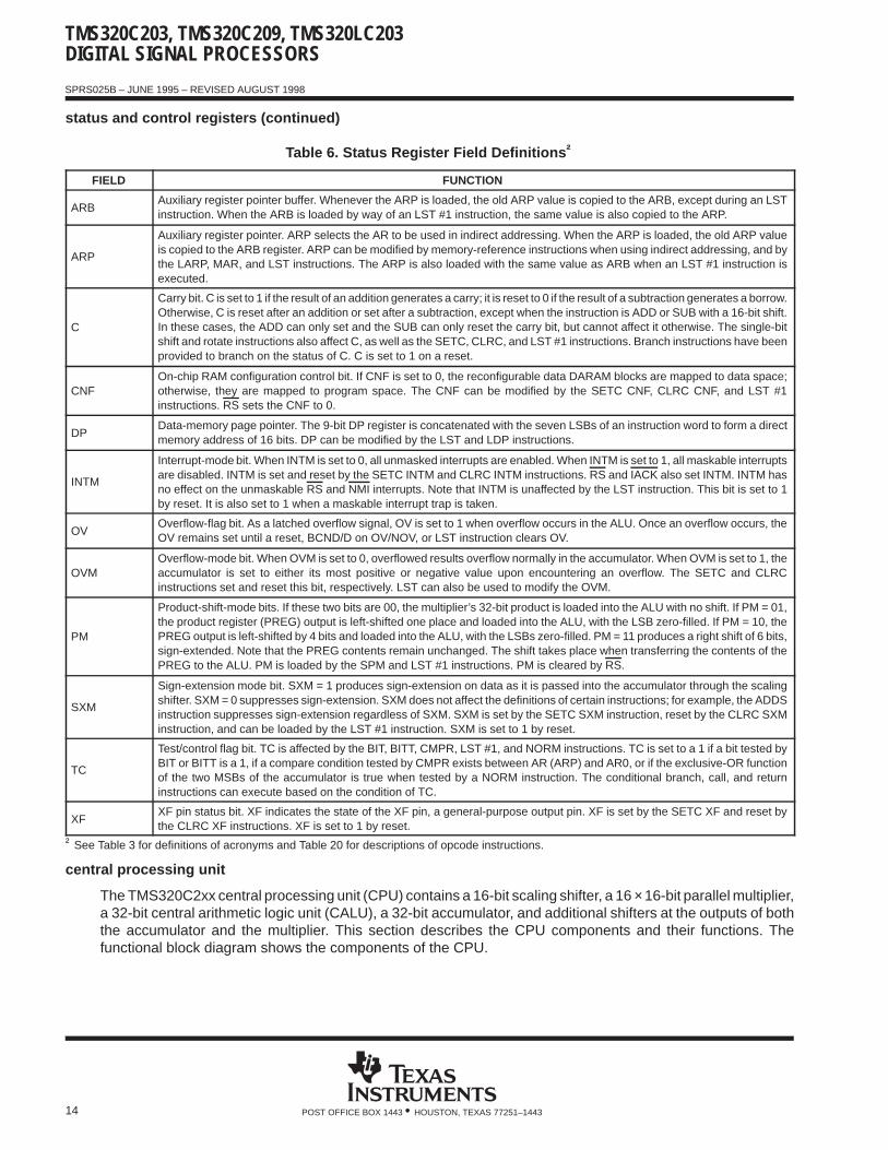
Table 6. Status Register Field Definitions †
FIELD FUNCTION
ARBAuxiliary register pointer buffer. Whenever the ARP is loaded, the old ARP value is copied to the ARB, except during an LSTinstruction. When the ARB is loaded by way of an LST #1 instruction, the same value is also copied to the ARP.
ARP
Auxiliary register pointer. ARP selects the AR to be used in indirect addressing. When the ARP is loaded, the old ARP valueis copied to the ARB register. ARP can be modified by memory-reference instructions when using indirect addressing, and bythe LARP, MAR, and LST instructions. The ARP is also loaded with the same value as ARB when an LST #1 instruction isexecuted.
C
Carry bit. C is set to 1 if the result of an addition generates a carry; it is reset to 0 if the result of a subtraction generates a borrow.Otherwise, C is reset after an addition or set after a subtraction, except when the instruction is ADD or SUB with a 16-bit shift.In these cases, the ADD can only set and the SUB can only reset the carry bit, but cannot affect it otherwise. The single-bitshift and rotate instructions also affect C, as well as the SETC, CLRC, and LST #1 instructions. Branch instructions have beenprovided to branch on the status of C. C is set to 1 on a reset.
CNFOn-chip RAM configuration control bit. If CNF is set to 0, the reconfigurable data DARAM blocks are mapped to data space;otherwise, they are mapped to program space. The CNF can be modified by the SETC CNF, CLRC CNF, and LST #1instructions. RS sets the CNF to 0.
DPData-memory page pointer. The 9-bit DP register is concatenated with the seven LSBs of an instruction word to form a directmemory address of 16 bits. DP can be modified by the LST and LDP instructions.
INTM
Interrupt-mode bit. When INTM is set to 0, all unmasked interrupts are enabled. When INTM is set to 1, all maskable interruptsare disabled. INTM is set and reset by the SETC INTM and CLRC INTM instructions. RS and IACK also set INTM. INTM hasno effect on the unmaskable RS and NMI interrupts. Note that INTM is unaffected by the LST instruction. This bit is set to 1by reset. It is also set to 1 when a maskable interrupt trap is taken.
OVOverflow-flag bit. As a latched overflow signal, OV is set to 1 when overflow occurs in the ALU. Once an overflow occurs, theOV remains set until a reset, BCND/D on OV/NOV, or LST instruction clears OV.
OVMOverflow-mode bit. When OVM is set to 0, overflowed results overflow normally in the accumulator. When OVM is set to 1, theaccumulator is set to either its most positive or negative value upon encountering an overflow. The SETC and CLRCinstructions set and reset this bit, respectively. LST can also be used to modify the OVM.
PM
Product-shift-mode bits. If these two bits are 00, the multiplier’s 32-bit product is loaded into the ALU with no shift. If PM = 01,the product register (PREG) output is left-shifted one place and loaded into the ALU, with the LSB zero-filled. If PM = 10, thePREG output is left-shifted by 4 bits and loaded into the ALU, with the LSBs zero-filled. PM = 11 produces a right shift of 6 bits,sign-extended. Note that the PREG contents remain unchanged. The shift takes place when transferring the contents of thePREG to the ALU. PM is loaded by the SPM and LST #1 instructions. PM is cleared by RS.
SXM
Sign-extension mode bit. SXM = 1 produces sign-extension on data as it is passed into the accumulator through the scalingshifter. SXM = 0 suppresses sign-extension. SXM does not affect the definitions of certain instructions; for example, the ADDSinstruction suppresses sign-extension regardless of SXM. SXM is set by the SETC SXM instruction, reset by the CLRC SXMinstruction, and can be loaded by the LST #1 instruction. SXM is set to 1 by reset.
TC
Test/control flag bit. TC is affected by the BIT, BITT, CMPR, LST #1, and NORM instructions. TC is set to a 1 if a bit tested byBIT or BITT is a 1, if a compare condition tested by CMPR exists between AR (ARP) and AR0, or if the exclusive-OR functionof the two MSBs of the accumulator is true when tested by a NORM instruction. The conditional branch, call, and returninstructions can execute based on the condition of TC.
XFXF pin status bit. XF indicates the state of the XF pin, a general-purpose output pin. XF is set by the SETC XF and reset bythe CLRC XF instructions. XF is set to 1 by reset.
† See Table 3 for definitions of acronyms and Table 20 for descriptions of opcode instructions.
central processing unit
The TMS320C2xx central processing unit (CPU) contains a 16-bit scaling shifter, a 16 × 16-bit parallel multiplier,a 32-bit central arithmetic logic unit (CALU), a 32-bit accumulator, and additional shifters at the outputs of boththe accumulator and the multiplier. This section describes the CPU components and their functions. Thefunctional block diagram shows the components of the CPU.
TMS320C203, TMS320C209, TMS320LC203DIGITAL SIGNAL PROCESSORS
SPRS025B – JUNE 1995 – REVISED AUGUST 1998
15POST OFFICE BOX 1443 • HOUSTON, TEXAS 77251–1443
input scaling shifter
The TMS320C2xx provides a scaling shifter with a 16-bit input connected to the data bus and a 32-bit outputconnected to the CALU. This shifter operates as part of the path of data coming from program or data spaceto the CALU and requires no cycle overhead. It is used to align the 16-bit data coming from memory to the 32-bitCALU. This is necessary for scaling arithmetic as well as aligning masks for logical operations.
The scaling shifter produces a left shift of 0 to 16 on the input data. The LSBs of the output are filled with zeros;the MSBs can be either filled with zeros or sign-extended, depending upon the value of the SXM bit(sign-extension mode) of status register ST1. The shift count is specified by a constant embedded in theinstruction word or by a value in the temporary register (TREG). The shift count in the instruction allows forspecific scaling or alignment operations specific to that point in the code. The TREG base shift allows the scalingfactor to be adaptable to the system’s performance.
multiplier
The TMS320C2xx uses a 16 × 16-bit hardware multiplier that is capable of computing a signed or an unsigned32-bit product in a single machine cycle. All multiply instructions, except the MPYU (multiply unsigned)instruction, perform a signed multiply operation. That is, two numbers being multiplied are treated as2s-complement numbers, and the result is a 32-bit 2s-complement number. There are two registers associatedwith the multiplier: a 16-bit temporary register (TREG) that holds one of the operands for the multiplier, and a32-bit product register (PREG) that holds the product.
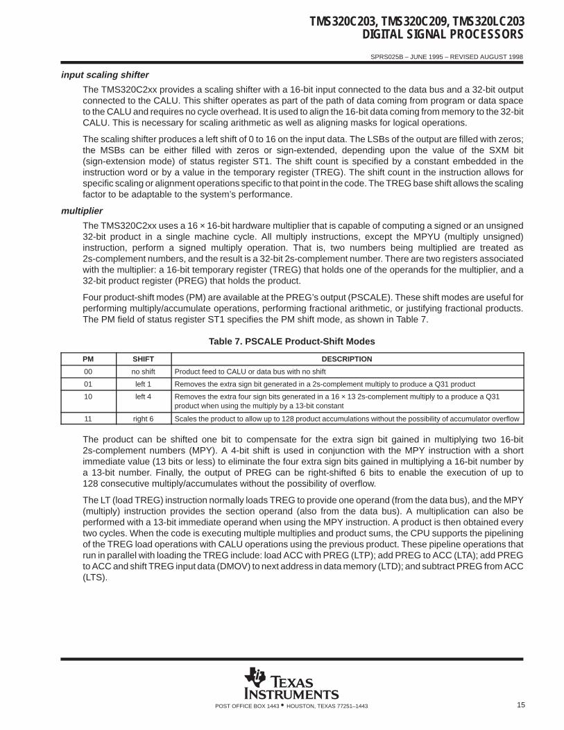
Four product-shift modes (PM) are available at the PREG’s output (PSCALE). These shift modes are useful forperforming multiply/accumulate operations, performing fractional arithmetic, or justifying fractional products.The PM field of status register ST1 specifies the PM shift mode, as shown in Table 7.
Table 7. PSCALE Product-Shift Modes
PM SHIFT DESCRIPTION
00 no shift Product feed to CALU or data bus with no shift
01 left 1 Removes the extra sign bit generated in a 2s-complement multiply to produce a Q31 product
10 left 4 Removes the extra four sign bits generated in a 16 × 13 2s-complement multiply to a produce a Q31product when using the multiply by a 13-bit constant
11 right 6 Scales the product to allow up to 128 product accumulations without the possibility of accumulator overflow
The product can be shifted one bit to compensate for the extra sign bit gained in multiplying two 16-bit2s-complement numbers (MPY). A 4-bit shift is used in conjunction with the MPY instruction with a shortimmediate value (13 bits or less) to eliminate the four extra sign bits gained in multiplying a 16-bit number bya 13-bit number. Finally, the output of PREG can be right-shifted 6 bits to enable the execution of up to128 consecutive multiply/accumulates without the possibility of overflow.
The LT (load TREG) instruction normally loads TREG to provide one operand (from the data bus), and the MPY(multiply) instruction provides the section operand (also from the data bus). A multiplication can also beperformed with a 13-bit immediate operand when using the MPY instruction. A product is then obtained everytwo cycles. When the code is executing multiple multiplies and product sums, the CPU supports the pipeliningof the TREG load operations with CALU operations using the previous product. These pipeline operations thatrun in parallel with loading the TREG include: load ACC with PREG (LTP); add PREG to ACC (LTA); add PREGto ACC and shift TREG input data (DMOV) to next address in data memory (LTD); and subtract PREG from ACC(LTS).
TMS320C203, TMS320C209, TMS320LC203DIGITAL SIGNAL PROCESSORS
SPRS025B – JUNE 1995 – REVISED AUGUST 1998
16 POST OFFICE BOX 1443 • HOUSTON, TEXAS 77251–1443
multiplier (continued)
Two multiply/accumulate instructions (MAC and MACD) fully utilize the computational bandwidth of themultiplier, allowing both operands to be processed simultaneously. The data for these operations can betransferred to the multiplier each cycle by way of the program and data buses. This facilitates single-cyclemultiply/accumulates when used with the repeat (RPT) instruction. In these instructions, the coefficientaddresses are generated by program address generation (PAGEN), while the data addresses are generatedby data-address generation (DAGEN). This allows the repeated instruction to sequentially access the valuesfrom the coefficient table and step through the data in any of the indirect addressing modes.
The MACD instruction, when repeated, supports filter constructs (weighted running averages) so that as thesum-of-products is executed, the sample data is shifted in memory to make room for the next sample and tothrow away the oldest sample.
The MPYU instruction performs an unsigned multiplication, which greatly facilitates extended-precisionarithmetic operations. The unsigned contents of TREG are multiplied by the unsigned contents of the addresseddata memory location, with the result placed in PREG. This allows the operands of greater than 16 bits to bebroken down into 16-bit words and processed separately to generate products of greater than 32 bits. TheSQRA (square/add) and SQRS (square/subtract) instructions pass the same value to both inputs of themultiplier for squaring a data-memory value.
After the multiplication of two 16-bit numbers, the 32-bit product is loaded into the 32-bit product register(PREG). The product from PREG can be transferred to the CALU or to data memory by way of the SPH (storeproduct-high register) and the SPL (store product-low register) instructions. Note: the transfer of PREG to eitherthe CALU or data memory passes through the product-scaling shifter (PSCALE) and is therefore affected bythe product-shift mode defined by PM bits in the ST1 register. This is important when saving PREG in aninterrupt-service-routine-context save as the PSCALE shift effects cannot be modeled in the restore operation.PREG can be cleared by executing the MPY #0 instruction. The product register can be restored by loading thesaved low half into TREG and executing the MPY #1 instruction. The high half is then loaded using the LPHinstruction.
central arithmetic logic unit
The TMS320C2xx central arithmetic logic unit (CALU) implements a wide range of arithmetic and logicalfunctions, the majority of which execute in a single clock cycle. This arithmetic logic unit (ALU) is referred to as“central” to differentiate it from a second ALU used for indirect-address-generation (called the ARAU). Once anoperation is performed in the CALU, the result is transferred to the accumulator (ACC), where additionaloperations, such as shifting, can occur. Data that is input to the CALU can be scaled by the input data-scalingshifter (ISCALE) when coming from one of the data buses (DRDB or PRDB) or scaled by PSCALE when comingfrom the multiplier.
The CALU is a general-purpose arithmetic/logic unit that operates on 16-bit words taken from data memory orderived from immediate instructions. In addition to the usual arithmetic instructions, the CALU can performBoolean operations, facilitating the bit manipulation ability required for a high-speed controller. One input to theCALU is always provided from the accumulator, and the other input can be provided from the product register(PREG) of the multiplier or the output of the scaling shifter (that has been read from data memory or from theACC). After the CALU has performed the arithmetic or logical operation, the result is stored in the accumulator.
The TMS320C2xx supports floating-point operations for applications requiring a large dynamic range. TheNORM (normalization) instruction is used to normalize fixed-point numbers contained in the accumulator byperforming left shifts. The four bits of the TREG define a variable shift through the scaling shifter for theLACT/ADDT/SUBT (load/add to/subtract from accumulator with shift specified by TREG) instructions. Theseinstructions are useful in floating-point arithmetic where a number needs to be denormalized—that is,floating-point to fixed-point conversion. They are also useful in the execution of an automatic gain control (AGC)going into a filter. The BITT (bit-test) instruction provides testing of a single bit of a word in data memory basedon the value contained in the four LSBs of TREG.

TMS320C203, TMS320C209, TMS320LC203DIGITAL SIGNAL PROCESSORS
SPRS025B – JUNE 1995 – REVISED AUGUST 1998
17POST OFFICE BOX 1443 • HOUSTON, TEXAS 77251–1443
central arithmetic logic unit (continued)
The CALU overflow-saturation mode can be enabled/disabled by setting/resetting the overflow mode (OVM)bit of ST0. When the CALU is in the overflow-saturation mode and an overflow occurs, the overflow flag is setand the accumulator is loaded with either the most positive or the most negative value representable in theaccumulator, depending upon the direction of the overflow. The value of the accumulator upon saturation is07FFFFFFFh (positive) or 080000000h (negative). If the OVM status register bit is reset and an overflow occurs,the overflowed results are loaded into the accumulator with modification. (Note that logical operations cannotresult in overflow.)
The CALU can execute a variety of branch instructions that depend on the status of the CALU and theaccumulator. These instructions can be executed conditionally, based on any meaningful combination of thesestatus bits. For overflow management, these conditions include the OV (branch on overflow) and EQ (branchon accumulator equal to zero). In addition, the BACC (branch to address in accumulator) instruction providesthe ability to branch to an address specified by the accumulator (computed goto). Bit-test instructions (BIT andBITT), which do not affect the accumulator, allow the testing of a specified bit of a word in data memory.
The CALU also has a carry bit that is set or reset depending on various operations within the device. The carrybit allows more efficient computation of extended-precision products and additions or subtractions. It is alsouseful in overflow management. The carry bit is affected by most arithmetic instructions as well as the single-bitshift and rotate instructions. It is not affected by accumulator loads, logical operations, or other suchnon-arithmetic or control instructions.
Additions to and subtractions from the accumulator:
C = 0: When the result of a subtraction generates a borrow.
When the result of an addition does not generate a carry. (Exception: When the ADD instruction isused with a shift of 16 and no carry is generated, the ADD instruction has no effect on C.)
C = 1: When the result of an addition generates a carry.
When the result of a subtraction does not generate a borrow. (Exception: When the SUB instruction is used with a shift of 16 and no borrow is generated, the SUB instruction has no effect on C.)
Single-bit shifts and rotations of the accumulator value. During a left shift or rotation, the most significantbit of the accumulator is passed to C; during a right shift or rotation, the least significant bit is passed to C.
Note: the carry bit is set to “1” on a hardware reset.
The ADDC (add to accumulator with carry) and SUBB (subtract from accumulator with borrow) instructionsprovide the use of the previous value of carry in their addition/subtraction operation.
The one exception to the operation of the carry bit is in the use of ADD with a shift count of 16 (add to highaccumulator) and SUB with a shift count of 16 (subtract from high accumulator) instructions. This case of theADD instruction can set the carry bit only if a carry is generated, and this case of the SUB instruction can resetthe carry bit only if a borrow is generated; otherwise, neither instruction affects it.
Two conditional operands, C and NC, are provided for branching, calling, returning, and conditionally executingbased upon the status of the carry bit. The SETC, CLRC, and LST #1 instructions also can be used to load thecarry bit. The carry bit is set to one on a hardware reset.
accumulator
The 32-bit accumulator is the registered output of the CALU. It can be split into two 16-bit segments for storagein data memory. Shifters at the output of the accumulator provide a left shift of 0 to 7 places. This shift isperformed while the data is being transferred to the data bus for storage. The contents of the accumulatorremain unchanged. When the post-scaling shifter is used on the high word of the accumulator (bits 16–31), theMSBs are lost and the LSBs are filled with bits shifted in from the low word (bits 0–15). When the post-scalingshifter is used on the low word, the LSBs are zero-filled.
TMS320C203, TMS320C209, TMS320LC203DIGITAL SIGNAL PROCESSORS
SPRS025B – JUNE 1995 – REVISED AUGUST 1998
18 POST OFFICE BOX 1443 • HOUSTON, TEXAS 77251–1443
accumulator (continued)
The SFL and SFR (in-place one-bit shift to the left/right) instructions and the ROL and ROR (rotate to theleft/right) instructions implement shifting or rotating of the accumulator contents through the carry bit. The SXMstatus register bit affects the definition of the SFR (shift accumulator right) instruction. When SXM = 1, SFRperforms an arithmetic right shift, maintaining the sign of the accumulator data. When SXM = 0, SFR performsa logical shift, shifting out the LSBs and shifting in a zero for the MSB. The SFL (shift accumulator left) instructionis not affected by the SXM bit and behaves the same in both cases, shifting out the MSB and shifting in a zero.RPT (repeat) instructions can be used with the shift and rotate instructions for multiple-bit shifts.
auxiliary registers and auxiliary-register arithmetic unit (ARAU)
The ’C2xx provides a register file containing eight auxiliary registers (AR0–AR7). The auxiliary registers areused for indirect addressing of the data memory or for temporary data storage. Indirect auxiliary-registeraddressing allows placement of the data memory address of an instruction operand into one of the auxiliaryregisters. These registers are referenced with a 3-bit auxiliary register pointer (ARP) that is loaded with a valuefrom 0 through 7, designated AR0 through AR7, respectively. The auxiliary registers and the ARP can be loadedfrom data memory, the ACC, the product register, or by an immediate operand defined in the instruction. Thecontents of these registers can also be stored in data memory or used as inputs to the CALU.
The auxiliary register file is connected to the ARAU. The ARAU can autoindex the current auxiliary register whilethe data memory location is being addressed. Indexing either by ±1 or by the contents of AR0 can be performed.As a result, accessing tables of information does not require the CALU for address manipulation; therefore, theCALU is free for other operations in parallel.
memory
The ’C2xx implements three separate address spaces for program memory, data memory, and I/O. Each spaceaccommodates a total of 64K 16-bit words. Within the 64K words of data space, the 256 to 32K words at thetop of the address range can be defined to be external global memory in increments of powers of two, asspecified by the contents of the global memory allocation register. Access to global memory is arbitrated usingthe global memory bus request (BR) signal.
On the ’C2xx, the first 96 (0–5Fh) data memory locations are allocated for memory-mapped registers or arereserved. This memory-mapped register space contains various control and status registers including those forthe CPU.
When using on-chip RAM, or high-speed external memory, the ’C2xx runs at full speed with no wait states. Theability of the DARAM to allow two accesses to be performed in one cycle, coupled with the parallel nature ofthe ’C2xx architecture, enables the device to perform three concurrent memory accesses in any given machinecycle. Externally, the READY line can be used to interface the ’C2xx to slower, less expensive external memory.Downloading programs from slow off-chip memory to on-chip RAM can speed processing while cutting systemcosts.
The ’C2xx DARAM allows writes to and reads from the RAM in the same cycle without the address restrictionsof the SARAM. The DARAM is configured in three blocks: block 0 (B0), block 1 (B1), and block 2 (B2).Block 1 consists of 256 words in data memory and block 2 consists of 32 words in data memory. Block 0 is a256-word block that can be configured as data or program memory. The SETC CNF (configure B0 as programmemory) and CLRC CNF (configure B0 as data memory) instructions allow dynamic configuration of thememory maps through software. When using Block 0 as program memory, instructions can be downloaded fromexternal program memory into on-chip RAM and then executed.
TMS320C203, TMS320C209, TMS320LC203DIGITAL SIGNAL PROCESSORS
SPRS025B – JUNE 1995 – REVISED AUGUST 1998
19POST OFFICE BOX 1443 • HOUSTON, TEXAS 77251–1443
memory (continued)
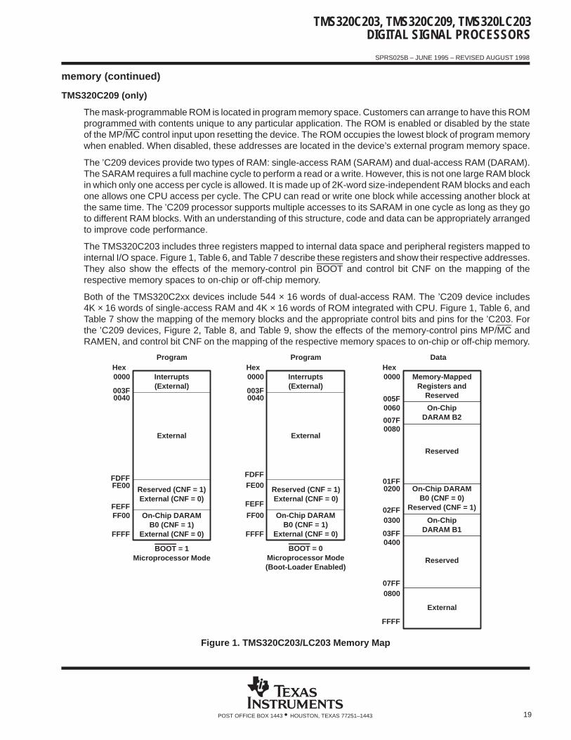
TMS320C209 (only)
The mask-programmable ROM is located in program memory space. Customers can arrange to have this ROMprogrammed with contents unique to any particular application. The ROM is enabled or disabled by the stateof the MP/MC control input upon resetting the device. The ROM occupies the lowest block of program memorywhen enabled. When disabled, these addresses are located in the device’s external program memory space.
The ’C209 devices provide two types of RAM: single-access RAM (SARAM) and dual-access RAM (DARAM).The SARAM requires a full machine cycle to perform a read or a write. However, this is not one large RAM blockin which only one access per cycle is allowed. It is made up of 2K-word size-independent RAM blocks and eachone allows one CPU access per cycle. The CPU can read or write one block while accessing another block atthe same time. The ’C209 processor supports multiple accesses to its SARAM in one cycle as long as they goto different RAM blocks. With an understanding of this structure, code and data can be appropriately arrangedto improve code performance.
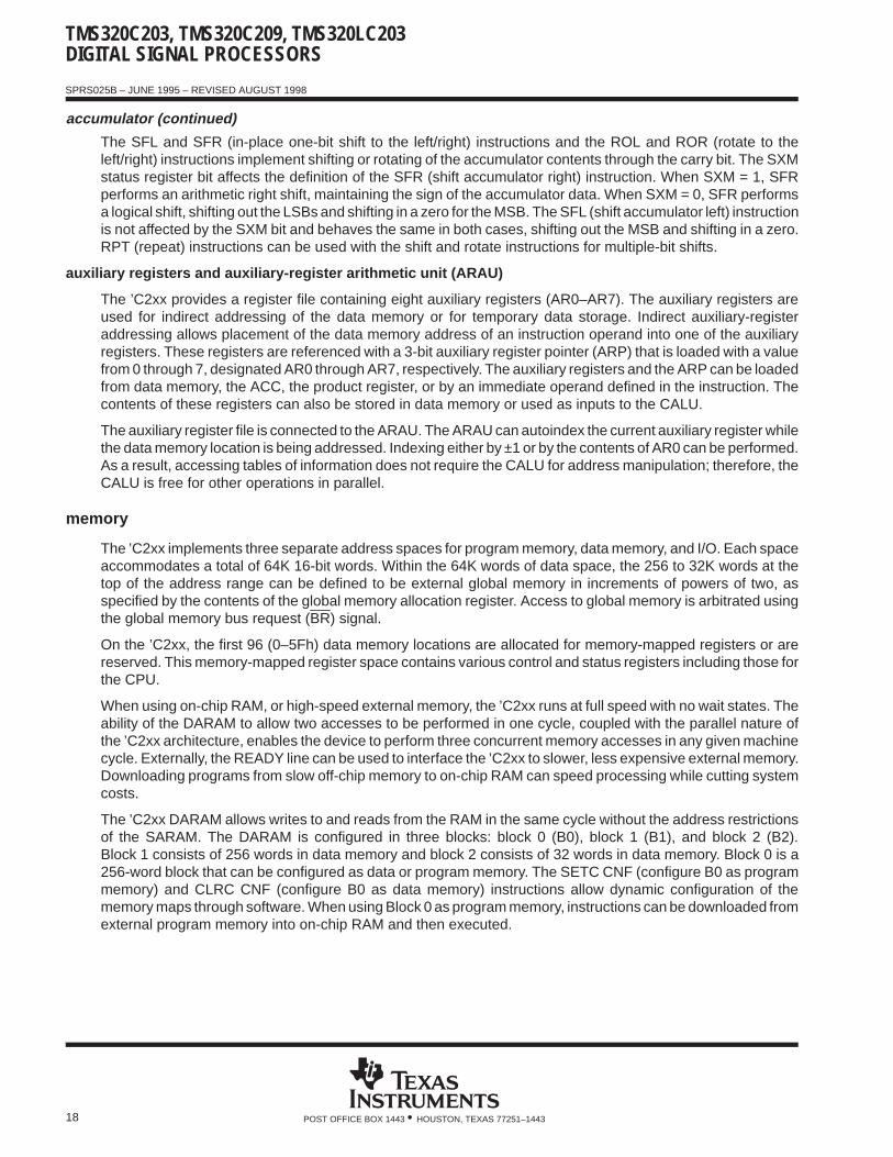
The TMS320C203 includes three registers mapped to internal data space and peripheral registers mapped tointernal I/O space. Figure 1, Table 6, and Table 7 describe these registers and show their respective addresses.They also show the effects of the memory-control pin BOOT and control bit CNF on the mapping of therespective memory spaces to on-chip or off-chip memory.
Both of the TMS320C2xx devices include 544 × 16 words of dual-access RAM. The ’C209 device includes4K × 16 words of single-access RAM and 4K × 16 words of ROM integrated with CPU. Figure 1, Table 6, andTable 7 show the mapping of the memory blocks and the appropriate control bits and pins for the ’C203. Forthe ’C209 devices, Figure 2, Table 8, and Table 9, show the effects of the memory-control pins MP/MC andRAMEN, and control bit CNF on the mapping of the respective memory spaces to on-chip or off-chip memory.
On-Chip DARAMB0 (CNF = 0)
Reserved (CNF = 1)
Interrupts(External)
0000
0040
External
FDFF
Reserved (CNF = 1)External (CNF = 0)
FE00
On-Chip DARAMB0 (CNF = 1)
External (CNF = 0)
FF00
FFFF
HexProgram
BOOT = 1Microprocessor Mode
Interrupts(External)
0000
0040
External
FDFFFE00
FEFF
On-Chip DARAMB0 (CNF = 1)
External (CNF = 0)
FF00
FFFF
HexProgram
BOOT = 0Microprocessor Mode(Boot-Loader Enabled)
Memory-MappedRegisters and
Reserved
0000Hex
Data
On-ChipDARAM B2
0060
Reserved
0080
01FF
On-ChipDARAM B1
0300
0200
0400
Reserved
07FF
External
0800
FFFF
Reserved (CNF = 1)External (CNF = 0)
003F
FEFF
005F
007F
02FF
03FF
003F
Figure 1. TMS320C203/LC203 Memory Map

TMS320C203, TMS320C209, TMS320LC203DIGITAL SIGNAL PROCESSORS
SPRS025B – JUNE 1995 – REVISED AUGUST 1998
20 POST OFFICE BOX 1443 • HOUSTON, TEXAS 77251–1443
memory (continued)
Table 8. TMS320C203/LC203 Memory Map Configurations †
BOOT CNFON-CHIP MEMORY OFF-CHIP MEMORY
BOOT CNFPROGRAM DATA I/O PROGRAM DATA I/O‡
0 0 — 0–7FF FF00–FFFF 0000–FFFF 800–FFFF 0–FEFF
0 1 FE00–FFFF§ 0–7FF FF00–FFFF 0000–FDFF 800–FFFF 0–FEFF
1 0 — 0–7FF FF00–FFFF 0000–FFFF 800–FFFF 0–FEFF
1 1 FE00–FFFF 0–7FF FF00–FFFF 0000–FDFF 800–FFFF 0–FEFF† Internal I/O locations 0FFE0h–0FFFFh are dedicated to the timer, serial-port control, wait-state generator registers, and reserved space.‡ FF00–FF0F are reserved for test purposes and should not be used.§ When BOOT = 0, the on-chip boot-loader at 0xFF00h is enabled. During boot time, memory address FE00–FFFF is reserved.
Table 9. TMS320C203/LC203 On-Chip Memory Map
DESCRIPTION OF MEMORY BLOCKDATA
ADDRESSPROG
ADDRESS BOOTCNFBIT
On-chip bootloader FF00–FFFFh low
256 × 16 word dual-access RAM (DARAM) (B0)0x100–0x1FFh¶
0x200–0x2FFh¶ 0
256 × 16 word DARAM (B0)0xFE00–0xFEFF¶
0xFF00–0xFFFF¶ 1
256 × 16 word DARAM (B1)0x300–0x3FFh¶
0x400–0x4FFh¶
32 × 16 word DARAM (B2) 0x60–0x7Fh¶ Each of these address pairs point to the same block of memory.
bootloader
The bootloader is used to transfer user code from an external global data memory source to program memoryautomatically at reset. This function is useful for initializing external RAM using external ROM. If the BOOT pinis sampled low during a hardware reset, a reset vector is internally generated forcing a branch to the on-chipboot ROM at address location FF00h. The code is read in parallel from an 8-bit-wide EPROM and transferredto the 16-bit-wide destination. The maximum size for the EPROM, is 32K words × 8-bits.# The first four bytestransferred define the destination address and program length. After the bootload is complete, the ’C203removes the boot ROM from the memory map. For a detailed description of bootloader functionality, refer tothe TMS320C2xx User’s Guide (literature number SPRU127).
# The address range 8000h – FEFFh equals 32 512 words.
TMS320C203, TMS320C209, TMS320LC203DIGITAL SIGNAL PROCESSORS
SPRS025B – JUNE 1995 – REVISED AUGUST 1998
21POST OFFICE BOX 1443 • HOUSTON, TEXAS 77251–1443
memory (continued)
Interrupts(External)
0000
External
0FFF
On-Chip SARAM(RAMEN = 1)
External(RAMEN = 0)
1000
1FFF
External
2000
Reserved (CNF = 1)External (CNF = 0)
FE00
On-Chip DARAMB0 (CNF = 1)
External (CNF = 0)
FF00
FFFF
HexProgram
MP/MC = 1Microprocessor Mode
Interrupts(On-Chip)
On-Chip ROM
On-Chip SARAM(RAMEN = 1)
External(RAMEN = 0)
External
On-Chip DARAMB0 (CNF = 1)
External (CNF = 0)
HexProgram
MP/MC = 0Microcomputer Mode
Memory-MappedRegisters and
Reserved
0000Hex
Data
On-ChipDARAM B2
0060
Reserved
0080
01FF
On-ChipDARAM B1
0300
On-Chip DARAMB0 (CNF = 0)
Reserved (CNF = 1)
0200
0400
Reserved
07FF
External(RAMEN = 0)
Reserved(RAMEN = 1)
0800
On-Chip SARAM(RAMEN = 1)
External(RAMEN = 0)
1000
External2000
FFFF
Reserved (CNF = 1)External (CNF = 0)
003F0040
FDFF
FEFF
0000
0FFF1000
1FFF2000
FE00
FF00
FFFF
003F0040
FDFF
FEFF
005F
007F
02FF
03FF
0FFF
1FFF
Figure 2. TMS320C209 Memory Map

TMS320C203, TMS320C209, TMS320LC203DIGITAL SIGNAL PROCESSORS
SPRS025B – JUNE 1995 – REVISED AUGUST 1998
22 POST OFFICE BOX 1443 • HOUSTON, TEXAS 77251–1443
memory (continued)
Table 10. TMS320C209 Memory Map Configurations †
MP/MC RAMEN CNFON-CHIP OFF-CHIP
MP/MC RAMEN CNFPROGRAM DATA I/O PROGRAM DATA I/O‡
0 1 0 0–1FFF 0–1FFF FFF0–FFFF 2000–FFFF 2000–FFFF 0–FFEF
0 1 10–1FFF
FE00–FFFF0–1FFF FFF0–FFFF 2000–FDFF 2000–FFFF 0–FFEF
0 0 0 0–0FFF 0–07FF FFF0–FFFF 1000–FFFF 0800–FFFF 0–FFEF
0 0 10–0FFF
FE00–FFFF0–07FF FFF0–FFFF 1000–FDFF 0800–FFFF 0–FFEF
1 1 0 1000–1FFF 0–1FFF FFF0–FFFF0–FFF
2000–FFFF2000–FFFF 0–FFEF
1 1 11000–1FFFFE00–FFFF
0–1FFF FFF0–FFFF0–FFF
2000–FDFF2000–FFFF 0–FFEF
1 0 0 0–07FF FFF0–FFFF 0–FFFF 0800–FFFF 0–FFEF
1 0 1 FE00–FFFF 0–07FF FFF0–FFFF 0–FDFF 0800–FFFF 0–FFEF† Internal I/O locations 0FFF0h–0FFFFh are dedicated to the timer, wait-state generator registers, and reserved space.‡ FF00–FF0F are reserved for test purposes and should not be used.
Table 11. TMS320C209 On-Chip Memory Map
DESCRIPTION OF MEMORY BLOCKDATA
ADDRESSPROG
ADDRESS MP/MCCNFBIT RAMEN
4K × 16 words of factory-masked ROM 0000–0FFFh low
256 × 16 words DARAM (B0)0x100–0x1FFh§
0x200–0x2FFh§ 0
256 × 16 words DARAM (B0)0xFE00–0xFEFF§
0xFF00–0xFFFF§ 1
256 × 16 words DARAM (B1)0x300–0x3FFh§
0x400–0x4FFh§
32 × 16 words DARAM (B2) 0x60–0x7Fh
4096 × 16 words single access RAM (SARAM) 0x1000–0x1FFFh 0x1000–0x1FFFh high§ Both of the addresses in each of these address pairs point to the same block of memory.

TMS320C203, TMS320C209, TMS320LC203DIGITAL SIGNAL PROCESSORS
SPRS025B – JUNE 1995 – REVISED AUGUST 1998
23POST OFFICE BOX 1443 • HOUSTON, TEXAS 77251–1443
memory (continued)
Table 12 shows the names, addresses, and functional descriptions of the TMS320C203 memory and I/Ointernally mapped registers.
Table 12. TMS320C203 Memory and I/O Internally Mapped Registers †
NAME ADDRESS DESCRIPTION
IMR DS@0004
Interrupt-mask register. IMR individually masks or enables the seven interrupts. Bit 0 shares the external interruptpins INT1 and HOLD. INT2 and INT3 share bit 1. Bit 2 ties to the timer interrupt, TINT. Bits 3 and 4, RINT andXINT, respectively, are for the synchronous serial port, SSP. Bit 5, TXRXINT, shares the transmit and receiveinterrupts for the asynchronous serial port, ASP. Bit 6 is reserved for monitor mode emulation operations andshould always be set to 0 except in conjunction with emulation monitor operations. Bits 7–15 are not used in theTMS320C203. IMR is set to 0 at reset.
GREG DS@0005Global memory allocation register. GREG specifies the size of the global memory space. GREG is set to 0 atreset.
IFR DS@0006
Interrupt-flag register. IFR indicates that the TMS320C203 has latched an interrupt from one of the sevenmaskable interrupts. Bit 0 shares the external interrupt INT1 and HOLD. INT2 and INT3 share bit 1. Bit 2 ties tothe timer interrupt, TINT. Bits 3 and 4, RINT and XINT, respectively, are for the synchronous serial port, SSP.Bit 5, TXRXINT, shares the transmit- and receive-interrupts for the asynchronous serial port, ASP. Bit 6 isreserved for monitor mode emulation operations and should always be set to 0 except in conjunction withemulation monitor operations. Writing a 1 to the respective interrupt bit clears an active flag and the respectivepending interrupt. Writing a 1 to an inactive flag has no effect. Bits 7–15 are not used in the TMS320C203. IMRis set to 0 at reset.
CLK IS@FFE8CLKOUT1 on or off. At reset, CLKOUT1 is configured as a zero for the pin to be active (on). If CLKOUT1 is a 1,the CLKOUT1 pin is turned off.
ICR IS@FFEC
Interrupt-control register. ICR is used to determine which interrupt is active since INT1 and HOLD share an inter-rupt vector as do INT1 and INT3. A portion of this register is for mask/unmask (similar to IMR) and another portionis for pending interrupts (similar to IFR). At reset, all bits are zeroed, enabling HOLD mode. The MODE bit is usedby the hold-generating circuit to determine if a HOLD or INT1 is active.
SDTR IS@FFF0 Synchronous serial-port (SSP) transmit and receive register
SSPCR IS@FFF1 Synchronous serial-port control register
ADTR IS@FFF4 Asynchronous serial-port (ASP) transmit and receive register
ASPCR IS@FFF5 Asynchronous serial-port control register. ASPCR controls the asynchronous serial port operation.
IOSR IS@FFF6 I/O status register. IOSR detects current levels (and changes with inputs) on pins IO0–IO3 and status of UART.
BRD IS@FFF7 Baud-rate divisor. Used to set baud rate of UART
TCR IS@FFF8Timer-control register. TCR contains the control bits that define the divide-down ratio, start/stop the timer, andreload the period. Also contained in TCR is the current count in the prescaler. Reset initializes the timerdivide-down ratio to 0 and starts the timer.
PRD IS@FFF9Timer-period register. PRD contains the 16-bit period that is loaded into the timer counter when the counterborrows or when the reload bit is activated. Reset initializes the PRD to 0xFFFF.
TIM IS@FFFA Timer-counter register. TIM contains the current 16-bit count of the timer. Reset initializes the TIM to 0xFFFF.
WSGR IS@FFFCWait-state-generator register. WSGR contains 12 control bits to enable 0, . . . ,7 wait states to program, data, andI/O space. Reset initializes the WSGR to 0x0FFFh.
† During on-chip I/O access, IS, RD, and WR are not visible at the pins (’C203 only).
TMS320C203, TMS320C209, TMS320LC203DIGITAL SIGNAL PROCESSORS
SPRS025B – JUNE 1995 – REVISED AUGUST 1998
24 POST OFFICE BOX 1443 • HOUSTON, TEXAS 77251–1443
memory (continued)
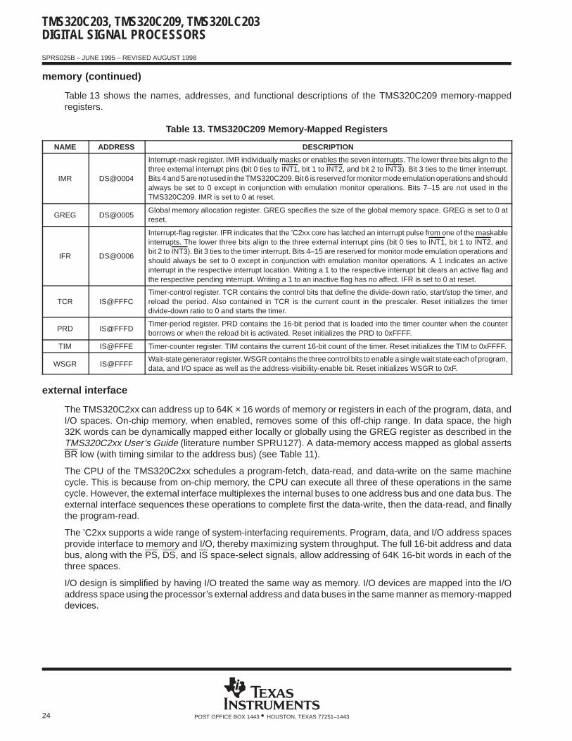
Table 13 shows the names, addresses, and functional descriptions of the TMS320C209 memory-mappedregisters.
Table 13. TMS320C209 Memory-Mapped Registers
NAME ADDRESS DESCRIPTION
IMR DS@0004
Interrupt-mask register. IMR individually masks or enables the seven interrupts. The lower three bits align to thethree external interrupt pins (bit 0 ties to INT1, bit 1 to INT2, and bit 2 to INT3). Bit 3 ties to the timer interrupt.Bits 4 and 5 are not used in the TMS320C209. Bit 6 is reserved for monitor mode emulation operations and shouldalways be set to 0 except in conjunction with emulation monitor operations. Bits 7–15 are not used in theTMS320C209. IMR is set to 0 at reset.
GREG DS@0005Global memory allocation register. GREG specifies the size of the global memory space. GREG is set to 0 atreset.
IFR DS@0006
Interrupt-flag register. IFR indicates that the ’C2xx core has latched an interrupt pulse from one of the maskableinterrupts. The lower three bits align to the three external interrupt pins (bit 0 ties to INT1, bit 1 to INT2, andbit 2 to INT3). Bit 3 ties to the timer interrupt. Bits 4–15 are reserved for monitor mode emulation operations andshould always be set to 0 except in conjunction with emulation monitor operations. A 1 indicates an activeinterrupt in the respective interrupt location. Writing a 1 to the respective interrupt bit clears an active flag andthe respective pending interrupt. Writing a 1 to an inactive flag has no affect. IFR is set to 0 at reset.
TCR IS@FFFCTimer-control register. TCR contains the control bits that define the divide-down ratio, start/stop the timer, andreload the period. Also contained in TCR is the current count in the prescaler. Reset initializes the timerdivide-down ratio to 0 and starts the timer.
PRD IS@FFFDTimer-period register. PRD contains the 16-bit period that is loaded into the timer counter when the counterborrows or when the reload bit is activated. Reset initializes the PRD to 0xFFFF.
TIM IS@FFFE Timer-counter register. TIM contains the current 16-bit count of the timer. Reset initializes the TIM to 0xFFFF.
WSGR IS@FFFFWait-state generator register. WSGR contains the three control bits to enable a single wait state each of program,data, and I/O space as well as the address-visibility-enable bit. Reset initializes WSGR to 0xF.
external interface
The TMS320C2xx can address up to 64K × 16 words of memory or registers in each of the program, data, andI/O spaces. On-chip memory, when enabled, removes some of this off-chip range. In data space, the high32K words can be dynamically mapped either locally or globally using the GREG register as described in theTMS320C2xx User’s Guide (literature number SPRU127). A data-memory access mapped as global assertsBR low (with timing similar to the address bus) (see Table 11).
The CPU of the TMS320C2xx schedules a program-fetch, data-read, and data-write on the same machinecycle. This is because from on-chip memory, the CPU can execute all three of these operations in the samecycle. However, the external interface multiplexes the internal buses to one address bus and one data bus. Theexternal interface sequences these operations to complete first the data-write, then the data-read, and finallythe program-read.
The ’C2xx supports a wide range of system-interfacing requirements. Program, data, and I/O address spacesprovide interface to memory and I/O, thereby maximizing system throughput. The full 16-bit address and databus, along with the PS, DS, and IS space-select signals, allow addressing of 64K 16-bit words in each of thethree spaces.
I/O design is simplified by having I/O treated the same way as memory. I/O devices are mapped into the I/Oaddress space using the processor’s external address and data buses in the same manner as memory-mappeddevices.
TMS320C203, TMS320C209, TMS320LC203DIGITAL SIGNAL PROCESSORS
SPRS025B – JUNE 1995 – REVISED AUGUST 1998
25POST OFFICE BOX 1443 • HOUSTON, TEXAS 77251–1443
external interface (continued)
The ’C2xx external parallel interface provides various control signals to facilitate interfacing to the device. TheR/W output signal is provided to indicate whether the current cycle is a read or a write. The STRB output signalprovides a timing reference for all external cycles. For convenience, the device also provides the RD and theWE output signals, which indicate a read and a write cycle, respectively, along with timing information for thosecycles. The availability of these signals minimizes external gating necessary for interfacing external devices tothe ’C2xx.
Interface to memory and I/O devices of varying speeds is accomplished by using the READY line. Whentransactions are made with slower devices, the ’C2xx processor waits until the other device completes itsfunction and signals the processor by way of the READY line. Once a ready indication is provided back to the’C2xx from the external device, execution continues. On the ’C209 device, the READY line is required (activehigh) to complete reads or writes to internal I/O-mapped registers. On the ’C203 devices, the READYline is required to be active high during boot time.
The bus-request (BR) signal is used in conjunction with the other ’C2xx interface signals to arbitrate externalglobal-memory accesses. Global memory is external data-memory space in which the BR signal is assertedat the beginning of the access. When an external global-memory device receives the bus request, it respondsby asserting the READY signal after the global memory access is arbitrated and the global access is completed.
The TMS320C2xx supports zero-wait-state reads on the external interface. However, to avoid bus conflicts,writes take two cycles. This allows the TMS320C2xx to buffer the transition of the data bus from input to output(or output to input) by a half cycle. In most systems, TMS320C2xx ratio of reads to writes is significantly largeto minimize the overhead of the extra cycle on writes.
Wait states can be generated when accessing slower external resources. The wait states operate onmachine-cycle boundaries and are initiated either by using READY or by using the software wait-stategenerator. READY can be used to generate any number of wait states.
interrupts and subroutines
The ’C2xx implements three general-purpose interrupts, INT3–INT1, along with reset (RS) and thenonmaskable interrupt (NMI), which are available for external devices to request the attention of the processor.Internal interrupts are generated by the synchronous serial port (RINT and XINT) (’C203 only), theasynchronous serial port (TXRXINT) (’C203 only), the timer (TINT), the UART, and the software-interrupt(TRAP, INTR and NMI) instructions. Interrupts are prioritized with RS having the highest priority, followed byNMI, and timer (TINT) (for ’C209) or UART (for ’C203) having the lowest priority. Additionally, any interrupt,except RS and NMI, can be individually masked with a dedicated bit in the interrupt mask register (IMR) andcan be cleared, set, or tested using its own dedicated bit in the interrupt flag register (IFR). The reset and NMIfunctions are not maskable.
All interrupt vector locations are on two-word boundaries so that branch instructions can be accommodated inthose locations if desired.
A built-in mechanism protects multicycle instructions from interrupts. If an interrupt occurs during a multicycleinstruction, the interrupt is not processed until the instruction completes execution. This mechanism applies toinstructions that are repeated (using the RPT instruction) and to instructions that become multicycle becauseof wait states.
Each time an interrupt is serviced or a subroutine is entered, the program counter (PC) is pushed onto an internalhardware stack, providing a mechanism for returning to the previous context. The stack contains eight locations,allowing interrupts or subroutines to be nested up to eight-levels deep.

TMS320C203, TMS320C209, TMS320LC203DIGITAL SIGNAL PROCESSORS
SPRS025B – JUNE 1995 – REVISED AUGUST 1998
26 POST OFFICE BOX 1443 • HOUSTON, TEXAS 77251–1443
reset
The TMS320C203 provides an active-low reset (RS) only, while the TMS320C209 provides both an RS and anRS.
RS and RS, the TMS320C209 resets, are not synchronized. A minimum pulse duration of six cycles ensuresthat an asynchronous reset signal resets the device. Either RS or RS can reset the device with RS being activehigh and RS being active low. The TMS320C2xx fetches its first instruction approximately sixteen cycles afterthe rising edge of RS (either ’C203 or ’C209) or falling edge of RS (’C209 only).
Please note that the reset action halts all operations whether they are completed or not. Therefore, the stateof the system and its data cannot be maintained through the reset operation. For example, if the device is writingto an external resource when the reset is initiated, the write is aborted. This can and will corrupt data in systemresources. It is, therefore, necessary to reinitialize the system after a reset.
power-down modes
The ’C2xx implements several power-down modes in which the ’C2xx core enters a dormant state anddissipates considerably less power. A power-down mode is invoked either by executing the IDLE instruction orby driving the HOLD (’C203 only) input low and executing HOLD mode. When the HOLD signal initiates thepower-down mode, on-chip peripherals continue to operate; this power-down mode is terminated when HOLDgoes inactive (’C203 only).
While the ’C2xx is in a power-down mode, all of its internal contents are maintained; this allows operation tocontinue unaltered when the power-down mode is terminated. All CPU activities are halted when the IDLEinstruction is executed, but the CLKOUT1 pin remains active depending on the status of the interrupt-control(IC) register (’C203 only). The peripheral circuits continue to operate, allowing peripherals such as serial portsand timers to take the CPU out of its powered-down state. A power-down mode, when initiated by an IDLEinstruction, is terminated upon receipt of an interrupt.
software-controlled wait-state generator
Due to the fast cycle time of the TMS320C2xx devices, it is often necessary to operate with wait states tointerface with external logic and memory. For many systems, one wait state is adequate.
TMS320C209
When operating the TMS320C209 at full speed, it is difficult to respond fast enough to provide a READY-basedwait state for the first cycle. For this reason, the TMS320C209 includes a simple software-controlled wait-stategenerator to provide the first wait state.
The software-controlled wait-state generator can be programmed to generate the first wait state for a givenexternal space. The wait-state generator (WSGR) has four wait-state bits: AVIS, DATA (DSWS), PROG(PSWS), and I/O (ISWS). The wait-state generator inserts a wait state to a given memory space if the respectivebit is set to 1, regardless of the condition of the READY signal. Then, READY can be used to further extend thewait states. The AVIS bit differs from the other WSGR bits because it does not generate a wait state but enablesthe address-visibility mode of the ’C209. This mode allows the internal program address to be presented to theaddress bus when this bus is not used for an external access. The WSGR bits are initially set to 1 by reset sothat the device can operate from slow memory. After initialization, the AVIS bit should be set to 0 for productionsystems to reduce power and noise. The WSGR register (shown in Table 14 and Table 15) resides at I/O port0xFFFFh.
TMS320C203, TMS320C209, TMS320LC203DIGITAL SIGNAL PROCESSORS
SPRS025B – JUNE 1995 – REVISED AUGUST 1998
27POST OFFICE BOX 1443 • HOUSTON, TEXAS 77251–1443
software-controlled wait-state generator (continued)
Table 14. TMS320C209 Wait-State Generator Control Register (WSGR)
15 4 3 2 1 0
FFFFh Reserved AVIS ISWS DSWS PSWS
0 W–1 W–1 W–1 W–1
Legend: 0 = Always read as zeros, R = Read Access, W= Write Access, – n = Value after reset
Table 15. Bit Functions of the TMS320C209 Wait-State Generator Control Register (WSGR)
BIT NO. BIT NAME DESCRIPTION
0 PSWS
External program-space wait-state bit on. When active, PSWS = 1 applies one wait state to all reads to off-chipprogram space (writes always take at least two cycles regardless of PSWS or READY). The memory cycle canbe further extended using the READY signal. However, the READY signal does not override the wait stategenerated by PSWS. This bit is set to 1 (active) by reset (RS or RS).
1 DSWS
External data-space wait-state bit on. When active, DSWS = 1 applies one wait state to all reads to off-chipdata space (writes always take at least two cycles regardless of DSWS or READY). The memory cycle canbe further extended using the READY signal. However, the READY signal does not override the wait stategenerated by DSWS. This bit is set to 1 (active) by reset (RS or RS).
2 ISWS
External input-/output-space wait-state bit on. When active, ISWS = 1 applies one wait state to all reads tooff-chip I/O space (writes always take at least two cycles regardless of ISWS or READY). The memory cyclecan be further extended using the READY signal. However, the READY signal does not override the wait stategenerated by ISWS. This bit is set to 1 (active) by reset (RS or RS).
3 AVIS
Address visibility mode. When active high, AVIS presents the internal program address out of thelogic-interface address bus if the bus is not currently used in an external memory operation. The internaladdress is presented to provide a trace mechanism of internal code operation. Therefore, the memory-controlsignals are not active. AVIS is set to 1 (active) by reset (RS or RS). AVIS should be deactivated in productionsystems to reduce system power and noise.
15–4 Reserved Always read as zeros.
TMS320C203
The software wait-state generator can be programmed to generate between zero and seven wait states for agiven space. The WSGR has 12 bits: three DATA, six PROGRAM, and three I/O. The wait-state generatorinserts a wait state(s) to a given memory space based on the value of the three bits, regardless of the conditionof the READY signal. The READY signal can be used to extend the wait state further. All bits are set to 1 at resetso that the device can operate from slow memory from reset. The WSGR register (shown in Table 16, Table 17and Table 18) resides at I/O port 0xFFFCh.
Table 16. TMS320C203 Wait-State Generator Control Register (WSGR)
15 14 13 12 11 10 9 8 7 6 5 4 3 2 1 0
FFFCh Reserved ISWS DSWS PSUWS PSLWS
0 R/W–111 R/W–111 R/W–111 R/W–111
Legend: 0 = Always read as zeros, R = Read Access, W= Write Access, – n = Value after reset
TMS320C203, TMS320C209, TMS320LC203DIGITAL SIGNAL PROCESSORS
SPRS025B – JUNE 1995 – REVISED AUGUST 1998
28 POST OFFICE BOX 1443 • HOUSTON, TEXAS 77251–1443
software-controlled wait-state generator (continued)
TMS320C203 (continued)
Table 17. Bit Functions of the TMS320C203 Wait-State Generator Control Register (WSGR)
BITS NAME DESCRIPTION
2–0 PSLWS
External program-space wait states (lower). PSLWS determines that between 0–7 wait states are applied to allreads and writes to off-chip lower-program-space address (0h–7FFFh). The memory cycle can be furtherextended using the READY signal. The READY signal does not override the wait states generated by PSLWS.Bits 2–0 are set to 1 (active) by reset (RS).
5–3 PSUWS
External program-space wait states (upper). PSUWS determines that between 0–7 wait states are applied to allreads and writes to off-chip upper-program-space address (8000h–0FFFFh). The memory cycle can be furtherextended using the READY signal. The READY signal does not override the wait states generated by PSUWS.Bits 5–3 are set to 1 (active) by reset (RS).
8–6 DSWSExternal data-space wait states. DSWS determines that between 0–7 wait states are applied to all reads andwrites to off-chip data space. The memory cycle can be further extended using the READY signal. The READYsignal does not override the wait states generated by DSWS. Bits 8–6 are set to 1 (active) by reset (RS).
11–9 ISWSExternal input/output-space wait state. ISWS determines that between 0–7 wait states are applied to all readsand writes to off-chip I/O space. The memory cycle can be further extended using the READY signal. The READYsignal does not override the wait states generated by ISWS. Bits 11–9 are set to 1 (active) by reset (RS).
15–12 Reserved Always read as zeros.
Table 18. Bit Settings for TMS320C203 Wait-State(s) Programming
PSLWS, PSUWS, DSWS, OR ISWS BITS WAIT STATES FOR PROGRAM, DATA, OR I /O
000 0
001 1
010 2
011 3
100 4
101 5
110 6
111 7
timer
The TMS320C203 includes a 20-bit timer, implemented with a 16-bit main counter (TIM), and a 4-bit prescalercounter (PSC). The count values are written into the 16-bit period register (PRD), and the 4-bit timer divide-downregister (TDDR). This timer clocks between one-half and one thirty-second the machine rate of the device itself,depending upon the programmable timer’s divide-down ratio. This timer can be stopped, restarted, reset, ordisabled by specific status bits.
The timer can be used to generate CPU interrupts periodically. The timer is decremented by one at everyCLKOUT1 cycle. A timer interrupt (TINT) and a pulse equal to the duration of a CLKOUT1 cycle on the externalTOUT pin are generated each time the counter decrements to zero. The timer, therefore, provides a convenientmean of performing periodic I/O or other functions.
TMS320C209 input clock options
The TMS320C209 includes two clock options. The first option (÷2) operates the CPU at half the input clock rate.The second option (×2) doubles the input clock and phase-locks the output clock with the input clock. The÷2 mode is enabled by tying the CLKMOD pin low. The ×2 mode is enabled by tying the CLKMOD pin high.
The clock-doubler option of the ’C209 uses an internal phase-locked loop (PLL). The PLL requiresapproximately 2500 cycles to lock. The rising edge of RS (or falling edge of RS) must be delayed until at leastthree cycles after the PLL has stabilized. Accordingly, a switch from ÷2 to ×2 mode should not be made while
TMS320C203, TMS320C209, TMS320LC203DIGITAL SIGNAL PROCESSORS
SPRS025B – JUNE 1995 – REVISED AUGUST 1998
29POST OFFICE BOX 1443 • HOUSTON, TEXAS 77251–1443
TMS320C209 input clock options (continued)
the processor is running because the internal clock generator can generate minimum clock pulse widthspecification violations. The RS or RS signals should be in their active state if the CLKMOD pin is changed.
TMS320C203 input clock options
The TMS320C203 provides multiple clock modes of: ÷2, ×1, ×2, ×4. The clock-mode configuration cannot bedynamically changed without executing another reset. The operation of the PLL circuit is affected by theoperating voltage of the device. If the device is operating at 5 V, then the PLL5V signal should be tied high. For3.3-V operation, PLL5V should be tied low.
synchronous serial port (TMS320C203 only)
A full-duplex, bidirectional, 16-bit on-chip synchronous serial port provides direct communication with serialdevices such as CODECs, serial analog-to-digital converters (A/Ds), and other serial systems. The interfacesignals are compatible with CODECs and many other serial devices. The serial port can also be used forintercommunication between processors in multiprocessing applications.
Both receive and transmit operations have a four-deep first-in-first-out (FIFO). The advantage of having a FIFOis to alleviate the CPU from being loaded with the task of servicing a transmit-data or receive-data on everyinterrupt, thereby, allowing a continuous communications stream of 16-bit data packets. The continuous modeprovides operation that once initiated, requires no further frame synchronization pulses when transmitting atmaximum packet frequency. The maximum transmission rate for both transmit and receive operations is CPUspeed divided by two or CLKOUT1(frequency)/2. Therefore, the maximum rate is 20 Mbps at 25 ns and14.28 Mbps at 35 ns. The serial port is fully static and functions at arbitrarily low clocking frequencies. Whenthe serial ports are in reset, the device can be configured to shut off the serial port internal clocks, allowing thedevice to run in a lower-power mode of operation.
Three signals are necessary to connect the transmit pins of the transmitting device with the receive pins of thereceiving device for data transmission. The transmit-serial-data signal (DX) sends the actual data. Thetransmit-frame-synchronization signal (FSX) initiates the transfer (at the beginning of the packet), and thetransmit-clock signal (CLKX) clocks the bit transfer. The corresponding pins on the receiving device are DR,FSR and CLKR, respectively.
asynchronous serial port (TMS320C203 only)
The universal asynchronous serial port (UART) is full-duplex, and transmits and receives 8-bit data only. Fortransmit and receive, there is one start bit and one or two configurable stop bits by way of the asynchronousserial-port control register (ASPCR). Double-buffering or transmit/receive data is used in all modes. Baud-rategeneration uses the BRD (baud-rate divisor) register to obtain the baud rate. The maximum baud rate is2.5 Mbps at 250000 characters per second (at 25-ns instruction cycle time).
The asynchronous serial port contains an autobaud-detection feature that allows it to automatically lock to theincoming data rate. Autobaud detection is enabled by setting the CAD bit in the ASPCR to 1 and the ADC bitin the I/O status register (IOSR) to 0. See the TMS320C2xx User’s Guide (literature number SPRU127) fordetails.
TMS320C2xx scan-based emulation
TMS320C203 devices incorporate scan-based emulation logic for code-and hardware-development support.Scan-based emulation allows the emulator to control the processor in the system without the use of intrusivecables to the full pinout of the device. The scan-based emulator communicates with the ’C203 by way of theIEEE 1149.1 (JTAG) interface. Note: The TMS320C203, like other DSPs in the TMS320C20x/TMS320C24xfamilies, does not include boundary scan. The scan chain of ’C203 device is useful for emulation functions only.
TMS320C203, TMS320C209, TMS320LC203DIGITAL SIGNAL PROCESSORS
SPRS025B – JUNE 1995 – REVISED AUGUST 1998
30 POST OFFICE BOX 1443 • HOUSTON, TEXAS 77251–1443
multiprocessing (TMS320C203 only)
The flexibility of the ’C2xx allows configurations to satisfy a wide range of system requirements; the device canbe used in a variety of system configurations, including but not limited to the following:
A standalone processor A multiprocessor with devices in parallel A slave/host multiprocessor with global memory space A peripheral processor interfaced by way of processor-controlled signals to another device
For multiprocessing applications, the ’C2xx has the capability of allocating global memory space andcommunicating with that space by way of the BR and READY control signals. Global memory is data memoryshared by more than one device. Global-memory access must be arbitrated. The 8-bit memory-mappedglobal-memory-allocation register (GREG) specifies part of the ’C2xx’s data memory as global externalmemory. The contents of the register determine the size of the global memory space. If the current instructionaddresses an operand within that space, BR is asserted to request control of the bus. The length of the memorycycle is controlled by the READY line.
The ’C203 supports direct-memory access (DMA) to its external program, data, and I/O spaces using the HOLDand HOLDA signals. Another device can take complete control of the ’C2xx’s external memory interface byasserting HOLD low and executing HOLD mode. This causes the ’C2xx to place its address, data, andmemory-control signals in the high-impedance state and assert HOLDA.
In ’C203, HOLD logic is not activated by hardware only. It is a combination of hardware interrupt (INT1 inMODE 0) and software instruction IDLE. See the TMS320C2xx User’s Guide (literature number SPRU127) fordetails.
instruction set
The ’C2xx microprocessor implements a comprehensive instruction set that supports both numeric-intensivesignal-processing operations and general-purpose applications, such as multiprocessing and high-speedcontrol. Source code for the ’C1x and ’C2x DSPs is upward-compatible with the ’C2xx.
For maximum throughput, the next instruction is prefetched while the current one is being executed. Becausethe same data lines are used to communicate to external data, program, or I/O space, the number of cycles aninstruction requires to execute varies depending upon whether the next data-operand fetch is from internal orexternal memory. Highest throughput is achieved by maintaining data memory on chip and using either internalor fast external program memory.
addressing modes
The ’C2xx instruction set provides four basic memory-addressing modes: direct, indirect, immediate andregister.
For direct addressing, the instruction word contains the lower seven bits of the data-memory address. This fieldis concatenated with the nine bits of the data-memory page pointer (DP) to form the 16-bit data-memoryaddress. Therefore, in the direct-addressing mode, data memory is effectively paged with a total of 512 pages,with each page containing 128 words.
Indirect addressing accesses data memory through the auxiliary registers. In this addressing mode, the addressof the instruction operand is contained in the currently selected auxiliary register. Eight auxiliary registers(AR0–AR7) provide flexible and powerful method of indirect addressing. To select a specific auxiliary register,the auxiliary register pointer (ARP) is loaded with a value from 0 to 7 for AR0 through AR7, respectively.

TMS320C203, TMS320C209, TMS320LC203DIGITAL SIGNAL PROCESSORS
SPRS025B – JUNE 1995 – REVISED AUGUST 1998
31POST OFFICE BOX 1443 • HOUSTON, TEXAS 77251–1443
addressing modes (continued)
There are seven types of indirect addressing: autoincrement or autodecrement, postindexing by either addingor subtracting the contents of AR0, single indirect addressing with no increment or decrement, and bit-reversedaddressing [used in fast Fourier transforms (FFTs)] with increment or decrement. All operations are performedon the current auxiliary register in the same cycle as the original instruction, following which the current auxiliaryregister and ARP can be modified.
In immediate addressing, the actual operand data is provided in a portion of the instruction word or words. Thereare two types of immediate addressing: long and short. In short immediate addressing, the data is containedin a portion of the bits in a single-word instruction. In long immediate addressing, the data is contained in thesecond word of a two-word instruction. The immediate-addressing mode is useful for data that does not needto be stored or used more than once during the course of program execution, such as initialization of values,constants, and so forth.
The register-addressing mode uses operands in CPU registers either explicitly, such as with a direct referenceto a specific register, or implicitly, with instructions that intrinsically reference certain registers. In either case,operand reference is simplified because 16-bit values can be used without specifying a full 16-bit operandaddress or immediate value.
repeat feature
The repeat function can be used with instructions (as defined in Table 20) such as multiply/accumulate (MACand MACD), block move (BLDD and BLPD), I/O transfer (IN/OUT), and table read/write (TBLR/TBLW). Theseinstructions, although normally multicycled, are pipelined when the repeat feature is used, and they effectivelybecome single-cycle instructions. For example, the table-read (TBLR) instruction may take three or more cyclesto execute, but when the instruction is repeated, a table location can be read every cycle.
The repeat counter (RPTC) is loaded with the addressed data memory location if direct or indirect addressingmode is used, and with an 8-bit immediate value if short immediate addressing is used. The RPTC register isloaded by the RPT instruction. This results in a maximum of N + 1 executions of a given instruction. RPTC iscleared by reset. Once an RPT instruction is decoded, all interrupts including NMI (excluding reset) are maskeduntil the completion of the repeat loop.
instruction set summary
This section summarizes the opcodes of the instruction set for the TMS320C2xx DSP devices. This instructionset is a superset of the ’C1x and ’C2x instruction sets. The instructions are alphabetized by the mnemonic. Thesymbols in Table 15 are used in the instruction set summary table (Table 20). The Texas Instruments ’C2xxassembler accepts ’C1x and ’C2x instructions.
For detailed information on instruction operation (that is, mnemonic syntax, words, cycles, and opcodes), seethe TMS320C2xx User’s Guide (literature number SPRU127).
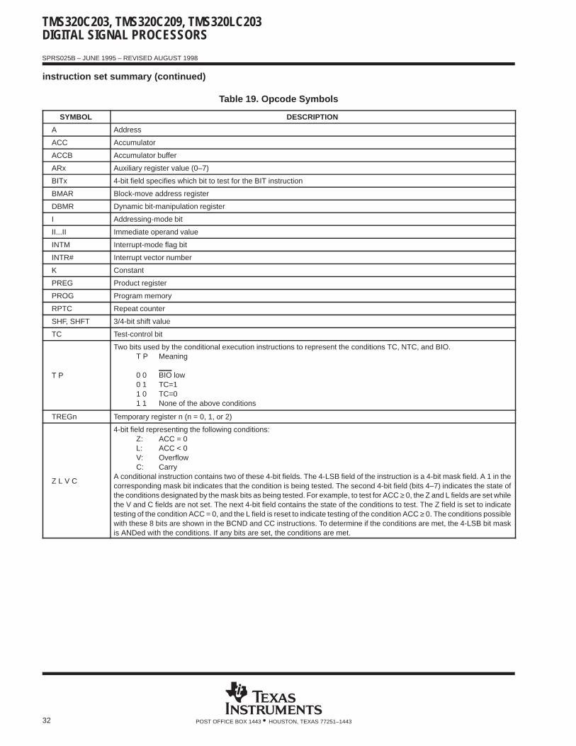
TMS320C203, TMS320C209, TMS320LC203DIGITAL SIGNAL PROCESSORS
SPRS025B – JUNE 1995 – REVISED AUGUST 1998
32 POST OFFICE BOX 1443 • HOUSTON, TEXAS 77251–1443
instruction set summary (continued)
Table 19. Opcode Symbols
SYMBOL DESCRIPTION
A Address
ACC Accumulator
ACCB Accumulator buffer
ARx Auxiliary register value (0–7)
BITx 4-bit field specifies which bit to test for the BIT instruction
BMAR Block-move address register
DBMR Dynamic bit-manipulation register
I Addressing-mode bit
II...II Immediate operand value
INTM Interrupt-mode flag bit
INTR# Interrupt vector number
K Constant
PREG Product register
PROG Program memory
RPTC Repeat counter
SHF, SHFT 3/4-bit shift value
TC Test-control bit
T P
Two bits used by the conditional execution instructions to represent the conditions TC, NTC, and BIO.T P Meaning
0 0 BIO low0 1 TC=11 0 TC=01 1 None of the above conditions
TREGn Temporary register n (n = 0, 1, or 2)
Z L V C
4-bit field representing the following conditions:Z: ACC = 0L: ACC < 0V: OverflowC: Carry
A conditional instruction contains two of these 4-bit fields. The 4-LSB field of the instruction is a 4-bit mask field. A 1 in thecorresponding mask bit indicates that the condition is being tested. The second 4-bit field (bits 4–7) indicates the state ofthe conditions designated by the mask bits as being tested. For example, to test for ACC ≥ 0, the Z and L fields are set whilethe V and C fields are not set. The next 4-bit field contains the state of the conditions to test. The Z field is set to indicatetesting of the condition ACC = 0, and the L field is reset to indicate testing of the condition ACC ≥ 0. The conditions possiblewith these 8 bits are shown in the BCND and CC instructions. To determine if the conditions are met, the 4-LSB bit maskis ANDed with the conditions. If any bits are set, the conditions are met.
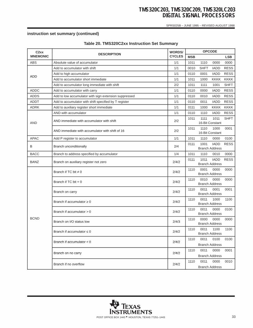
TMS320C203, TMS320C209, TMS320LC203DIGITAL SIGNAL PROCESSORS
SPRS025B – JUNE 1995 – REVISED AUGUST 1998
33POST OFFICE BOX 1443 • HOUSTON, TEXAS 77251–1443
instruction set summary (continued)
Table 20. TMS320C2xx Instruction Set Summary
C2xxDESCRIPTION
WORDS/ OPCODEMNEMONIC
DESCRIPTIONCYCLES MSB LSB
ABS Absolute value of accumulator 1/1 1011 1110 0000 0000
Add to accumulator with shift 1/1 0010 SHFT IADD RESS
ADDAdd to high accumulator 1/1 0110 0001 IADD RESS
ADDAdd to accumulator short immediate 1/1 1011 1000 KKKK KKKK
Add to accumulator long immediate with shift 2/2 1011 1111 1001 SHFT
ADDC Add to accumulator with carry 1/1 0110 0000 IADD RESS
ADDS Add to low accumulator with sign extension suppressed 1/1 0110 0010 IADD RESS
ADDT Add to accumulator with shift specified by T register 1/1 0110 0011 IADD RESS
ADRK Add to auxiliary register short immediate 1/1 0111 1000 KKKK KKKK
AND with accumulator 1/1 0110 1110 IADD RESS
AND immediate with accumulator with shift 2/21011 1111 1011 SHFT
ANDAND immediate with accumulator with shift 2/2
16-Bit Constant
AND immediate with accumulator with shift of 16 2/21011 1110 1000 0001
AND immediate with accumulator with shift of 16 2/216-Bit Constant
APAC Add P register to accumulator 1/1 1011 1110 0000 0100
B Branch unconditionally 2/40111 1001 IADD RESS
B Branch unconditionally 2/4Branch Address
BACC Branch to address specified by accumulator 1/4 1011 1110 0010 0000
BANZ Branch on auxiliary register not zero 2/4/20111 1011 IADD RESS
BANZ Branch on auxiliary register not zero 2/4/2Branch Address
Branch if TC bit ≠ 0 2/4/21110 0001 0000 0000
Branch if TC bit ≠ 0 2/4/2Branch Address
Branch if TC bit = 0 2/4/21110 0010 0000 0000
Branch if TC bit = 0 2/4/2Branch Address
Branch on carry 2/4/21110 0011 0001 0001
Branch on carry 2/4/2Branch Address
Branch if accumulator ≥ 0 2/4/21110 0011 1000 1100
Branch if accumulator ≥ 0 2/4/2Branch Address
Branch if accumulator > 0 2/4/21110 0011 0000 0100
Branch if accumulator > 0 2/4/2Branch Address
BCNDBranch on I/O status low 2/4/3
1110 0000 0000 0000Branch on I/O status low 2/4/3
Branch Address
Branch if accumulator ≤ 0 2/4/21110 0011 1100 1100
Branch if accumulator ≤ 0 2/4/2Branch Address
Branch if accumulator < 0 2/4/21110 0011 0100 0100
Branch if accumulator < 0 2/4/2Branch Address
Branch on no carry 2/4/21110 0011 0000 0001
Branch on no carry 2/4/2Branch Address
Branch if no overflow 2/4/21110 0011 0000 0010
Branch if no overflow 2/4/2Branch Address
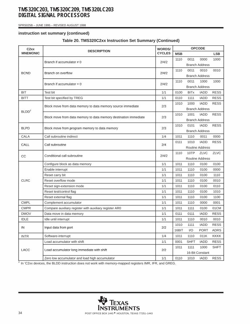
TMS320C203, TMS320C209, TMS320LC203DIGITAL SIGNAL PROCESSORS
SPRS025B – JUNE 1995 – REVISED AUGUST 1998
34 POST OFFICE BOX 1443 • HOUSTON, TEXAS 77251–1443
instruction set summary (continued)
Table 20. TMS320C2xx Instruction Set Summary (Continued)
C2xxDESCRIPTION
WORDS/ OPCODEMNEMONIC
DESCRIPTIONCYCLES MSB LSB
Branch if accumulator ≠ 0 2/4/21110 0011 0000 1000
Branch if accumulator ≠ 0 2/4/2Branch Address
BCND Branch on overflow 2/4/21110 0011 0010 0010
BCND Branch on overflow 2/4/2Branch Address
Branch if accumulator = 0 2/4/21110 0011 1000 1000
Branch if accumulator = 0 2/4/2Branch Address
BIT Test bit 1/1 0100 BITx IADD RESS
BITT Test bit specified by TREG 1/1 0110 1111 IADD RESS
†Block move from data memory to data memory source immediate 2/3
1010 1000 IADD RESS
BLDD†Block move from data memory to data memory source immediate 2/3
Branch AddressBLDD†
Block move from data memory to data memory destination immediate 2/31010 1001 IADD RESS
Block move from data memory to data memory destination immediate 2/3Branch Address
BLPD Block move from program memory to data memory 2/31010 0101 IADD RESS
BLPD Block move from program memory to data memory 2/3Branch Address
CALA Call subroutine indirect 1/4 1011 1110 0011 0000
CALL Call subroutine 2/40111 1010 IADD RESS
CALL Call subroutine 2/4Routine Address
CC Conditional call subroutine 2/4/21110 10TP ZLVC ZLVC
CC Conditional call subroutine 2/4/2Routine Address
Configure block as data memory 1/1 1011 1110 0100 0100
Enable interrupt 1/1 1011 1110 0100 0000
Reset carry bit 1/1 1011 1110 0100 1110
CLRC Reset overflow mode 1/1 1011 1110 0100 0010
Reset sign-extension mode 1/1 1011 1110 0100 0110
Reset test/control flag 1/1 1011 1110 0100 1010
Reset external flag 1/1 1011 1110 0100 1100
CMPL Complement accumulator 1/1 1011 1110 0000 0001
CMPR Compare auxiliary register with auxiliary register AR0 1/1 1011 1111 0100 01CM
DMOV Data move in data memory 1/1 0111 0111 IADD RESS
IDLE Idle until interrupt 1/1 1011 1110 0010 0010
IN Input data from port 2/21010 1111 IADD RESS
IN Input data from port 2/216BIT I/O PORT ADRS
INTR Software-interrupt 1/4 1011 1110 011K KKKK
Load accumulator with shift 1/1 0001 SHFT IADD RESS
LACC Load accumulator long immediate with shift 2/21011 1111 1000 SHFT
LACC Load accumulator long immediate with shift 2/216-Bit Constant
Zero low accumulator and load high accumulator 1/1 0110 1010 IADD RESS† In ’C2xx devices, the BLDD instruction does not work with memory-mapped registers IMR, IFR, and GREG.
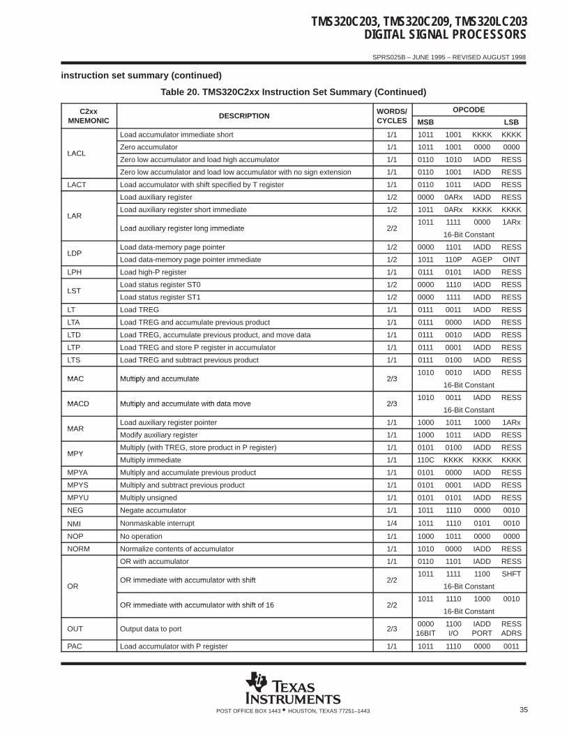
TMS320C203, TMS320C209, TMS320LC203DIGITAL SIGNAL PROCESSORS
SPRS025B – JUNE 1995 – REVISED AUGUST 1998
35POST OFFICE BOX 1443 • HOUSTON, TEXAS 77251–1443
instruction set summary (continued)
Table 20. TMS320C2xx Instruction Set Summary (Continued)
C2xxDESCRIPTION
WORDS/ OPCODEMNEMONIC
DESCRIPTIONCYCLES MSB LSB
Load accumulator immediate short 1/1 1011 1001 KKKK KKKK
LACLZero accumulator 1/1 1011 1001 0000 0000
LACLZero low accumulator and load high accumulator 1/1 0110 1010 IADD RESS
Zero low accumulator and load low accumulator with no sign extension 1/1 0110 1001 IADD RESS
LACT Load accumulator with shift specified by T register 1/1 0110 1011 IADD RESS
Load auxiliary register 1/2 0000 0ARx IADD RESS
LARLoad auxiliary register short immediate 1/2 1011 0ARx KKKK KKKK
LAR
Load auxiliary register long immediate 2/21011 1111 0000 1ARx
Load auxiliary register long immediate 2/216-Bit Constant
LDPLoad data-memory page pointer 1/2 0000 1101 IADD RESS
LDPLoad data-memory page pointer immediate 1/2 1011 110P AGEP OINT
LPH Load high-P register 1/1 0111 0101 IADD RESS
LSTLoad status register ST0 1/2 0000 1110 IADD RESS
LSTLoad status register ST1 1/2 0000 1111 IADD RESS
LT Load TREG 1/1 0111 0011 IADD RESS
LTA Load TREG and accumulate previous product 1/1 0111 0000 IADD RESS
LTD Load TREG, accumulate previous product, and move data 1/1 0111 0010 IADD RESS
LTP Load TREG and store P register in accumulator 1/1 0111 0001 IADD RESS
LTS Load TREG and subtract previous product 1/1 0111 0100 IADD RESS
MAC Multiply and accumulate 2/31010 0010 IADD RESS
MAC Multiply and accumulate 2/316-Bit Constant
MACD Multiply and accumulate with data move 2/31010 0011 IADD RESS
MACD Multiply and accumulate with data move 2/316-Bit Constant
MARLoad auxiliary register pointer 1/1 1000 1011 1000 1ARx
MARModify auxiliary register 1/1 1000 1011 IADD RESS
MPYMultiply (with TREG, store product in P register) 1/1 0101 0100 IADD RESS
MPYMultiply immediate 1/1 110C KKKK KKKK KKKK
MPYA Multiply and accumulate previous product 1/1 0101 0000 IADD RESS
MPYS Multiply and subtract previous product 1/1 0101 0001 IADD RESS
MPYU Multiply unsigned 1/1 0101 0101 IADD RESS
NEG Negate accumulator 1/1 1011 1110 0000 0010
NMI Nonmaskable interrupt 1/4 1011 1110 0101 0010
NOP No operation 1/1 1000 1011 0000 0000
NORM Normalize contents of accumulator 1/1 1010 0000 IADD RESS
OR with accumulator 1/1 0110 1101 IADD RESS
OR immediate with accumulator with shift 2/21011 1111 1100 SHFT
OROR immediate with accumulator with shift 2/2
16-Bit Constant
OR immediate with accumulator with shift of 16 2/21011 1110 1000 0010
OR immediate with accumulator with shift of 16 2/216-Bit Constant
OUT Output data to port 2/3000016BIT
1100I/O
IADDPORT
RESSADRS
PAC Load accumulator with P register 1/1 1011 1110 0000 0011

TMS320C203, TMS320C209, TMS320LC203DIGITAL SIGNAL PROCESSORS
SPRS025B – JUNE 1995 – REVISED AUGUST 1998
36 POST OFFICE BOX 1443 • HOUSTON, TEXAS 77251–1443
instruction set summary (continued)
Table 20. TMS320C2xx Instruction Set Summary (Continued)
C2xxDESCRIPTION
WORDS/ OPCODEMNEMONIC
DESCRIPTIONCYCLES MSB LSB
POP Pop top of stack to low accumulator 1/1 1011 1110 0011 0010
POPD Pop top of stack to data memory 1/1 1000 1010 IADD RESS
PSHD Push data-memory value onto stack 1/1 0111 0110 IADD RESS
PUSH Push low accumulator onto stack 1/1 1011 1110 0011 1100
RET Return from subroutine 1/4 1110 1111 0000 0000
RETC Conditional return from subroutine 1/4/2 1110 11TP ZLVC ZLVC
ROL Rotate accumulator left 1/1 1011 1110 0000 1100
ROR Rotate accumulator right 1/1 1011 1110 0000 1101
RPTRepeat instruction as specified by data-memory value 1/1 0000 1011 IADD RESS
RPTRepeat instruction as specified by immediate value 1/1 1011 1011 KKKK KKKK
SACH Store high accumulator with shift 1/1 1001 1SHF IADD RESS
SACL Store low accumulator with shift 1/1 1001 0SHF IADD RESS
SAR Store auxiliary register 1/1 1000 0ARx IADD RESS
SBRK Subtract from auxiliary register short immediate 1/1 0111 1100 KKKK KKKK
Set carry bit 1/1 1011 1110 0100 1111
Configure block as program memory 1/1 1011 1110 0100 0101
Disable interrupt 1/1 1011 1110 0100 0001
SETC Set overflow mode 1/1 1011 1110 0100 0011
Set test/control flag 1/1 1011 1110 0100 1011
Set external flag XF 1/1 1011 1110 0100 1101
Set sign-extension mode 1/1 1011 1110 0100 0111
SFL Shift accumulator left 1/1 1011 1110 0000 1001
SFR Shift accumulator right 1/1 1011 1110 0000 1010
SPAC Subtract P register from accumulator 1/1 1011 1110 0000 0101
SPH Store high-P register 1/1 1000 1101 IADD RESS
SPL Store low-P register 1/1 1000 1100 IADD RESS
SPM Set P register output shift mode 1/1 1011 1111 IADD RESS
SQRA Square and accumulate 1/1 0101 0010 IADD RESS
SQRS Square and subtract previous product from accumulator 1/1 0101 0011 IADD RESS
SSTStore status register ST0 1/1 1000 1110 IADD RESS
SSTStore status register ST1 1/1 1000 1111 IADD RESS
SPLK Store long immediate to data memory 2/21010 1110 IADD RESS
SPLK Store long immediate to data memory 2/216-Bit Constant
Subtract from accumulator long immediate with shift 2/21011 1111 1010 SHFT
Subtract from accumulator long immediate with shift 2/216-Bit Constant
SUB Subtract from accumulator with shift 1/1 0011 SHFT IADD RESS
Subtract from high accumulator 1/1 0110 0101 IADD RESS
Subtract from accumulator short immediate 1/1 1011 1010 KKKK KKKK

TMS320C203, TMS320C209, TMS320LC203DIGITAL SIGNAL PROCESSORS
SPRS025B – JUNE 1995 – REVISED AUGUST 1998
37POST OFFICE BOX 1443 • HOUSTON, TEXAS 77251–1443
instruction set summary (continued)
Table 20. TMS320C2xx Instruction Set Summary (Continued)
C2xxDESCRIPTION
WORDS/ OPCODEMNEMONIC
DESCRIPTIONCYCLES MSB LSB
SUBB Subtract from accumulator with borrow 1/1 0110 0100 IADD RESS
SUBC Conditional subtract 1/1 0000 1010 IADD RESS
SUBS Subtract from low accumulator with sign extension suppressed 1/1 0110 0110 IADD RESS
SUBT Subtract from accumulator with shift specified by TREG 1/1 0110 0111 IADD RESS
TBLR Table read 1/3 1010 0110 IADD RESS
TBLW Table write 1/3 1010 0111 IADD RESS
TRAP Software interrupt 1/4 1011 1110 0101 0001
Exclusive-OR with accumulator 1/1 0110 1100 IADD RESS
Exclusive OR immediate with accumulator with shift 2/21011 1111 1101 SHFT
XORExclusive-OR immediate with accumulator with shift 2/2
16-Bit Constant
Exclusive OR immediate with accumulator with shift of 16 2/21011 1110 1000 0011
Exclusive-OR immediate with accumulator with shift of 16 2/216-Bit Constant
ZALR Zero low accumulator and load high accumulator with rounding 1/1 0110 1000 IADD RESS
development support
Texas Instruments (TI ) offers an extensive line of development tools for the ’C2xx generation of DSPs,including tools to evaluate the performance of the processors, generate code, develop algorithmimplementations, and fully integrate and debug software and hardware modules.
The following products support development of ’C2xx-based applications:
Software Development Tools:Assembler/LinkerSimulatorOptimizing ANSI C CompilerApplication AlgorithmsC/Assembly Debugger and Code Profiler
Hardware Development Tools:Emulator XDS510 (supports ’C2xx multiprocessor system debug)
The TMS320 Family Development Support Reference Guide (literature number SPRU011) containsinformation about development support products for all TMS320 family member devices, includingdocumentation. Refer to this document for further information about TMS320 documentation or any otherTMS320 support products from Texas Instruments. There is also an additional document, the TMS320Third-Party Support Reference Guide (literature number SPRU052), which contains information aboutTMS320-related products from other companies in the industry. To receive copies of TMS320 literature, contactthe Literature Response Center at 800/477-8924.
See Table 21 for complete listings of development support tools for the ’C2xx. For information on pricing andavailability, contact the nearest TI field sales office or authorized distributor.
TI is a trademark of Texas Instruments Incorporated.
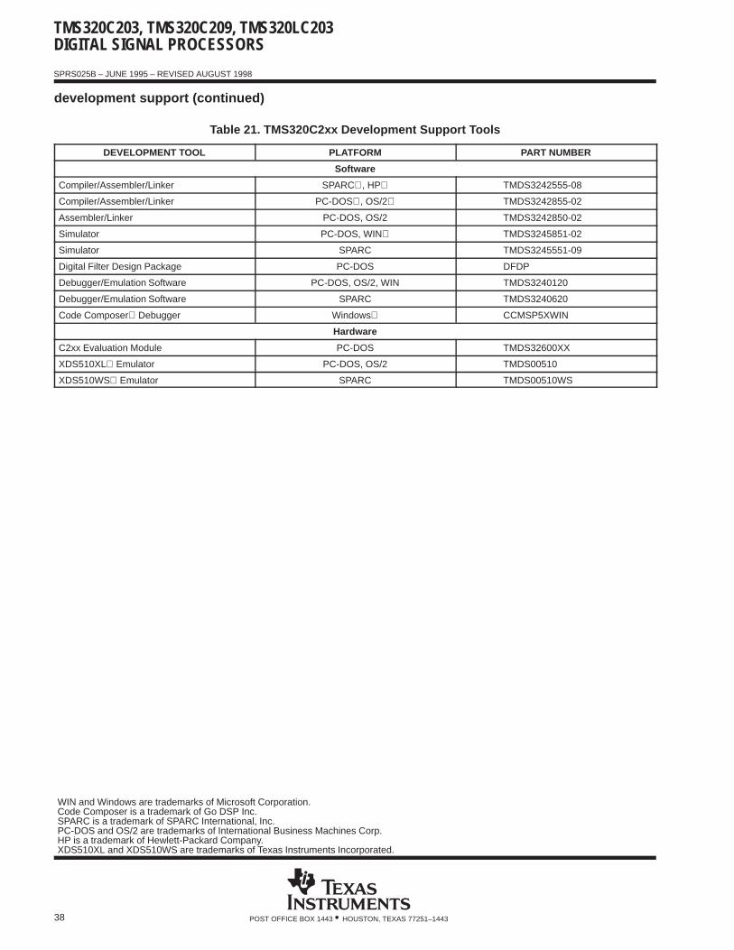
TMS320C203, TMS320C209, TMS320LC203DIGITAL SIGNAL PROCESSORS
SPRS025B – JUNE 1995 – REVISED AUGUST 1998
38 POST OFFICE BOX 1443 • HOUSTON, TEXAS 77251–1443
development support (continued)
Table 21. TMS320C2xx Development Support Tools
DEVELOPMENT TOOL PLATFORM PART NUMBER
Software
Compiler/Assembler/Linker SPARC , HP TMDS3242555-08
Compiler/Assembler/Linker PC-DOS , OS/2 TMDS3242855-02
Assembler/Linker PC-DOS, OS/2 TMDS3242850-02
Simulator PC-DOS, WIN TMDS3245851-02
Simulator SPARC TMDS3245551-09
Digital Filter Design Package PC-DOS DFDP
Debugger/Emulation Software PC-DOS, OS/2, WIN TMDS3240120
Debugger/Emulation Software SPARC TMDS3240620
Code Composer Debugger Windows CCMSP5XWIN
Hardware
C2xx Evaluation Module PC-DOS TMDS32600XX
XDS510XL Emulator PC-DOS, OS/2 TMDS00510
XDS510WS Emulator SPARC TMDS00510WS
WIN and Windows are trademarks of Microsoft Corporation.Code Composer is a trademark of Go DSP Inc.SPARC is a trademark of SPARC International, Inc.PC-DOS and OS/2 are trademarks of International Business Machines Corp.HP is a trademark of Hewlett-Packard Company.XDS510XL and XDS510WS are trademarks of Texas Instruments Incorporated.
TMS320C203, TMS320C209, TMS320LC203DIGITAL SIGNAL PROCESSORS
SPRS025B – JUNE 1995 – REVISED AUGUST 1998
39POST OFFICE BOX 1443 • HOUSTON, TEXAS 77251–1443
device and development support tool nomenclature
To designate the stages in the product development cycle, Texas Instruments assigns prefixes to the partnumbers of all TMS320 devices and support tools. Each TMS320 member has one of three prefixes: TMX, TMP,and TMS. Texas Instruments recommends two of three possible prefix designators for its support tools: TMDXand TMDS. These prefixes represent evolutionary stages of product development from engineering prototypes(TMX/TMDX) through fully qualified production devices/tools (TMS/TMDS). This development flow is definedbelow.
Device Development Evolutionary Flow:
TMX Experimental device that is not necessarily representative of the final device’s electricalspecifications
TMP Final silicon die that conforms to the device’s electrical specifications but has not completedquality and reliability verification
TMS Fully-qualified production device
Support Tool Development Evolutionary Flow:
TMDX Development support product that has not yet completed Texas Instruments internal qualificationtesting
TMDS Fully qualified development support product
TMX and TMP devices and TMDX development support tools are shipped against the following disclaimer:
“Developmental product is intended for internal evaluation purposes.”
TMS devices and TMDS development support tools have been fully characterized, and the quality and reliabilityof the device have been fully demonstrated. Texas Instruments standard warranty applies.
Predictions show that prototype devices (TMX or TMP) will have a greater failure rate than the standardproduction devices. Texas Instruments recommends that these devices not be used in any production systembecause their expected end-use failure rate is still undefined. Only qualified production devices are to be used.

TMS320C203, TMS320C209, TMS320LC203DIGITAL SIGNAL PROCESSORS
SPRS025B – JUNE 1995 – REVISED AUGUST 1998
40 POST OFFICE BOX 1443 • HOUSTON, TEXAS 77251–1443
device and development support tool nomenclature (continued)
TI device nomenclature also includes a suffix with the device family name. This suffix indicates the package type(for example, PZ or PN) and temperature range (for example, L). The following figures provide a legend forreading the complete device name for any TMS320 family member.
PREFIX TEMPERATURE RANGE (DEFAULT: 0 °C TO 70°C)
TMS 320 C 203 PZ (L)
TMX= experimental deviceTMP= prototype deviceTMS= qualified device
DEVICE FAMILY320 = TMS320 Family
TECHNOLOGY
L = 0°C to 70°CA = –40°C to 85°C
PACKAGE TYPE †PZ = 100-pin plastic TQFPPN = 80-pin TQFP
C = CMOSE = CMOS EPROMF = CMOS Flash EEPROMLC = Low-Voltage CMOS (3.3 V)VC= Low-Voltage CMOS (3 V)
DEVICE’2xx DSP
203‡206209240
(B)
BOOT-LOADER OPTION ‡
† TQFP = Thin Quad Flat Package‡ The TMS320C203 is a boot-loader device without the B option.
Figure 3. TMS320C2xx Device Nomenclature
documentation support
Extensive documentation supports all of the TMS320 family generations of devices from product announcementthrough applications development. The types of documentation available include: data sheets, such as thisdocument, with design specifications; complete user’s guides for all devices and development support tools;and hardware and software applications.
For general background information on DSPs and TI devices, see the three-volume publication Digital SignalProcessing Applications With the TMS320 Family (literature numbers SPRA012, SPRA016, and SPRA017).Also available is the Calculation of TMS320C2xx Power Dissipation application report (literature numberSPRA088).
A series of DSP textbooks is published by Prentice-Hall and John Wiley & Sons to support digital signalprocessing research and education. The TMS320 newsletter, Details on Signal Processing, is publishedquarterly and distributed to update TMS320 customers on product information. The TMS320 DSP bulletin boardservice (BBS) provides access to information pertaining to the TMS320 family, including documentation, sourcecode and object code for many DSP algorithms and utilities. The BBS can be reached at 281/274-2323.
Information regarding TI DSP products is also available on the Worldwide Web at http://www.ti.com uniformresource locator (URL).
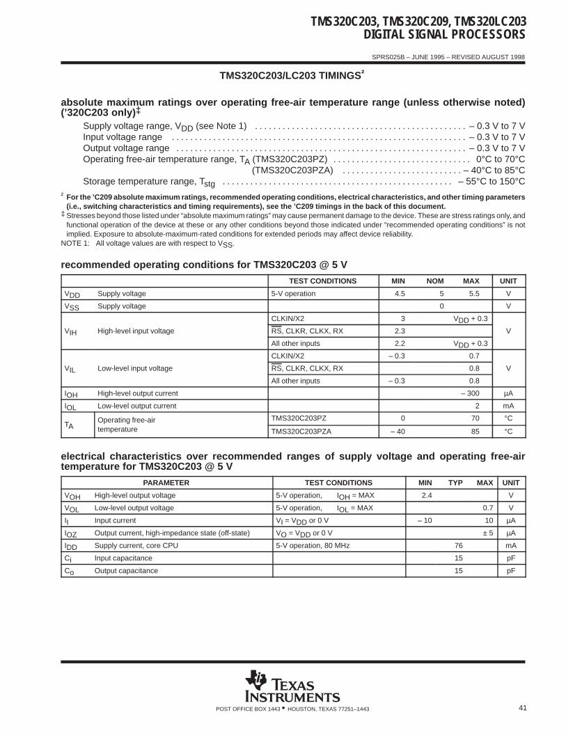
TMS320C203, TMS320C209, TMS320LC203DIGITAL SIGNAL PROCESSORS
SPRS025B – JUNE 1995 – REVISED AUGUST 1998
41POST OFFICE BOX 1443 • HOUSTON, TEXAS 77251–1443
TMS320C203/LC203 TIMINGS†
absolute maximum ratings over operating free-air temperature range (unless otherwise noted)(’320C203 only) ‡
Supply voltage range, VDD (see Note 1) – 0.3 V to 7 V. . . . . . . . . . . . . . . . . . . . . . . . . . . . . . . . . . . . . . . . . . . . . . Input voltage range – 0.3 V to 7 V. . . . . . . . . . . . . . . . . . . . . . . . . . . . . . . . . . . . . . . . . . . . . . . . . . . . . . . . . . . . . . . . Output voltage range – 0.3 V to 7 V. . . . . . . . . . . . . . . . . . . . . . . . . . . . . . . . . . . . . . . . . . . . . . . . . . . . . . . . . . . . . . . Operating free-air temperature range, TA (TMS320C203PZ) 0°C to 70°C. . . . . . . . . . . . . . . . . . . . . . . . . . . . . .
(TMS320C203PZA) – 40°C to 85°C. . . . . . . . . . . . . . . . . . . . . . . . . . Storage temperature range, Tstg – 55°C to 150°C. . . . . . . . . . . . . . . . . . . . . . . . . . . . . . . . . . . . . . . . . . . . . . . . . .
† For the ’C209 absolute maximum ratings, recommended operating conditions, electrical characteristics, and other timing paramete rs(i.e., switching characteristics and timing requirements), see the ’C209 timings in the back of this document.
‡ Stresses beyond those listed under “absolute maximum ratings” may cause permanent damage to the device. These are stress ratings only, andfunctional operation of the device at these or any other conditions beyond those indicated under “recommended operating conditions” is notimplied. Exposure to absolute-maximum-rated conditions for extended periods may affect device reliability.
NOTE 1: All voltage values are with respect to VSS.
recommended operating conditions for TMS320C203 @ 5 V
TEST CONDITIONS MIN NOM MAX UNIT
VDD Supply voltage 5-V operation 4.5 5 5.5 V
VSS Supply voltage 0 V
CLKIN/X2 3 VDD + 0.3
VIH High-level input voltage RS, CLKR, CLKX, RX 2.3 V
All other inputs 2.2 VDD + 0.3
CLKIN/X2 – 0.3 0.7
VIL Low-level input voltage RS, CLKR, CLKX, RX 0.8 V
All other inputs – 0.3 0.8
IOH High-level output current – 300 µA
IOL Low-level output current 2 mA
TAOperating free-air TMS320C203PZ 0 70 °C
TAg
temperature TMS320C203PZA – 40 85 °C
electrical characteristics over recommended ranges of supply voltage and operating free-airtemperature for TMS320C203 @ 5 V
PARAMETER TEST CONDITIONS MIN TYP MAX UNIT
VOH High-level output voltage 5-V operation, IOH = MAX 2.4 V
VOL Low-level output voltage 5-V operation, IOL = MAX 0.7 V
II Input current VI = VDD or 0 V – 10 10 µA
IOZ Output current, high-impedance state (off-state) VO = VDD or 0 V ± 5 µA
IDD Supply current, core CPU 5-V operation, 80 MHz 76 mA
Ci Input capacitance 15 pF
Co Output capacitance 15 pF
TMS320C203, TMS320C209, TMS320LC203DIGITAL SIGNAL PROCESSORS
SPRS025B – JUNE 1995 – REVISED AUGUST 1998
42 POST OFFICE BOX 1443 • HOUSTON, TEXAS 77251–1443
TMS320C203/LC203 TIMINGS† (CONTINUED)
absolute maximum ratings over operating free-air temperature range (unless otherwise noted)(’320LC203 only) ‡
Supply voltage range, VDD (see Note 1) – 0.3 V to 5 V. . . . . . . . . . . . . . . . . . . . . . . . . . . . . . . . . . . . . . . . . . . . . . Input voltage range – 0.3 V to 5 V. . . . . . . . . . . . . . . . . . . . . . . . . . . . . . . . . . . . . . . . . . . . . . . . . . . . . . . . . . . . . . . . Output voltage range – 0.3 V to 5 V. . . . . . . . . . . . . . . . . . . . . . . . . . . . . . . . . . . . . . . . . . . . . . . . . . . . . . . . . . . . . . . Operating free-air temperature range, TA (TMS320LC203PZA) – 40°C to 85°C. . . . . . . . . . . . . . . . . . . . . . . . . Storage temperature range, Tstg – 55°C to 150°C. . . . . . . . . . . . . . . . . . . . . . . . . . . . . . . . . . . . . . . . . . . . . . . . . .
† For the ’C209 absolute maximum ratings, recommended operating conditions, electrical characteristics, and other timing paramete rs(i.e., switching characteristics and timing requirements), see the ’C209 timings in the back of this document.
‡ Stresses beyond those listed under “absolute maximum ratings” may cause permanent damage to the device. These are stress ratings only, andfunctional operation of the device at these or any other conditions beyond those indicated under “recommended operating conditions” is notimplied. Exposure to absolute-maximum-rated conditions for extended periods may affect device reliability.
NOTE 1: All voltage values are with respect to VSS.
recommended operating conditions for TMS320LC203 @ 3.3 V
TEST CONDITIONS MIN NOM MAX UNIT
VDD Supply voltage 3.3-V operation 3 3.3 3.6 V
VSS Supply voltage 0 V
CLKIN/X2§ 2.5 VDD + 0.3
VIH High-level input voltage RS, CLKR, CLKX, RX 2 V
All other inputs 1.8 VDD + 0.3
VIL Low-level input voltage
CLKIN/X2, RS, READY,HOLD/INT1, INT2, INT3, NMI
– 0.3 0.4VIL g
All other inputs – 0.3 0.4
IOH High-level output current – 300 µA
IOL Low-level output current 2 mA
TA Operating free-air temperature TMS320LC203PZA – 40 85 °C§ Values derived from characterization data and not tested
electrical characteristics over recommended ranges of supply voltage and operating free-airtemperature for TMS320LC203 @ 3.3 V (TTL levels)
PARAMETER TEST CONDITIONS MIN TYP MAX UNIT
VOH High-level output voltage 3.3-V operation, IOH = MAX 2.4 V
VOL Low-level output voltage 3.3-V operation, IOL = MAX 0.4 V
II Input current VI = VDD or 0 V – 10 10 µA
IOZ Output current, high-impedance state (off-state) VO = VDD or 0 V ± 5 µA
IDD Supply current, core CPU 3.3-V operation, 40 MHz 22 mA
Ci Input capacitance 15 pF
Co Output capacitance 15 pF
Ii CLKIN input current Vi = VDD or 0 V – 350 350 µA
TMS320C203, TMS320C209, TMS320LC203DIGITAL SIGNAL PROCESSORS
SPRS025B – JUNE 1995 – REVISED AUGUST 1998
43POST OFFICE BOX 1443 • HOUSTON, TEXAS 77251–1443
PARAMETER MEASUREMENT INFORMATION FOR ’C203/’LC203
Tester PinElectronics
VLOAD
IOL
CT
IOH
OutputUnderTest
50 Ω
Where: IOL = 2 mA (all outputs)IOH = 300 µA (all outputs)VLOAD = 1.5 VCT = 60-pF typical load-circuit capacitance
Figure 4. Test Load Circuit
signal-transition levels
The data in this section is shown for both the 5-V version (’C203) and the 3.3-V version (’LC203). In each case,the 5-V data is shown followed by the 3.3-V data in parentheses. Note that some of the signals use differentreference voltages, see the recommended operating conditions tables for 5-V and 3.3-V devices. TTL-outputlevels are driven to a minimum logic-high level of 2.4 V (2.4 V) and to a maximum logic-low level of 0.7 V (0.4 V).
Figure 5 shows the TTL-level outputs.
0.7 V (0.4 V)20%
2.4 V (2.4 V)80%
Figure 5. TTL-Level Outputs
TTL-output transition times are specified as follows:
For a high-to-low transition, the level at which the output is said to be no longer high is below 80% of thetotal voltage range and lower and the level at which the output is said to be low is 20% of the total voltagerange and lower.
For a low-to-high transition, the level at which the output is said to be no longer low is 20% of the total voltagerange and higher and the level at which the output is said to be high is 80% of the total voltage range andhigher.
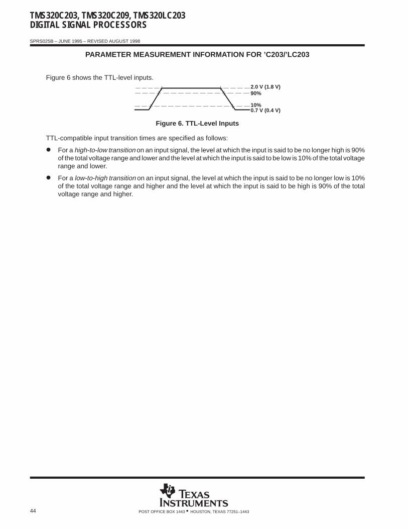
TMS320C203, TMS320C209, TMS320LC203DIGITAL SIGNAL PROCESSORS
SPRS025B – JUNE 1995 – REVISED AUGUST 1998
44 POST OFFICE BOX 1443 • HOUSTON, TEXAS 77251–1443
PARAMETER MEASUREMENT INFORMATION FOR ’C203/’LC203
Figure 6 shows the TTL-level inputs.
0.7 V (0.4 V)10%
2.0 V (1.8 V)90%
Figure 6. TTL-Level Inputs
TTL-compatible input transition times are specified as follows:
For a high-to-low transition on an input signal, the level at which the input is said to be no longer high is 90%of the total voltage range and lower and the level at which the input is said to be low is 10% of the total voltagerange and lower.
For a low-to-high transition on an input signal, the level at which the input is said to be no longer low is 10%of the total voltage range and higher and the level at which the input is said to be high is 90% of the totalvoltage range and higher.
TMS320C203, TMS320C209, TMS320LC203DIGITAL SIGNAL PROCESSORS
SPRS025B – JUNE 1995 – REVISED AUGUST 1998
45POST OFFICE BOX 1443 • HOUSTON, TEXAS 77251–1443
PARAMETER MEASUREMENT INFORMATION FOR ’C203/’LC203
timing parameter symbology
Timing parameter symbols used are created in accordance with JEDEC Standard 100-A. To shorten thesymbols, some of the pin names and other related terminology have been abbreviated as follows:
A Address or A[15:0] MS Memory strobe pins IS, DS, or PS
CI CLKIN/X2 R READY
CO CLKOUT1 RD Read cycle or RD
D Data or D[15:0] RS RESET pins RS or RS
FS FSX S STRB
H HOLD (’203 only) SCK Serial-port clock
HA HOLDA (’203 only) W Write cycle or WE
IN INTN; BIO, INT1–INT3, NMI
Lowercase subscripts and their meanings are: The following letters and symbols and their meanings are:
a access time H High
c cycle time (period) L Low
d delay time V Valid
dis disable time Z High impedance
en enable time X Unknown, changing, or don’t care level
f fall time
h hold time
r rise time
su setup time
t transition time
v valid time
w pulse duration (width)
general notes on timing parameters for ’C203/’LC203
All output signals from the TMS320C2xx devices (including CLKOUT1) are derived from an internal clock suchthat all output transitions for a given half cycle occur with a minimum of skewing relative to each other.
The signal combinations shown in the following timing diagrams may not necessarily represent actual cycles.For actual cycle examples, refer to the appropriate cycle description section of this data sheet.
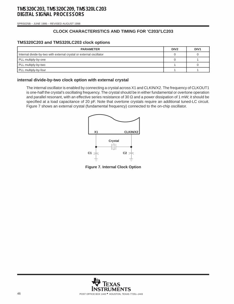
TMS320C203, TMS320C209, TMS320LC203DIGITAL SIGNAL PROCESSORS
SPRS025B – JUNE 1995 – REVISED AUGUST 1998
46 POST OFFICE BOX 1443 • HOUSTON, TEXAS 77251–1443
CLOCK CHARACTERISTICS AND TIMING FOR ’C203/’LC203
TMS320C203 and TMS320LC203 clock options
PARAMETER DIV2 DIV1
Internal divide-by-two with external crystal or external oscillator 0 0
PLL multiply-by-one 0 1
PLL multiply-by-two 1 0
PLL multiply-by-four 1 1
internal divide-by-two clock option with external crystal
The internal oscillator is enabled by connecting a crystal across X1 and CLKIN/X2. The frequency of CLKOUT1is one-half the crystal’s oscillating frequency. The crystal should be in either fundamental or overtone operationand parallel resonant, with an effective series resistance of 30 Ω and a power dissipation of 1 mW; it should bespecified at a load capacitance of 20 pF. Note that overtone crystals require an additional tuned-LC circuit.Figure 7 shows an external crystal (fundamental frequency) connected to the on-chip oscillator.
X1 CLKIN/X2
C1 C2
Crystal
Figure 7. Internal Clock Option
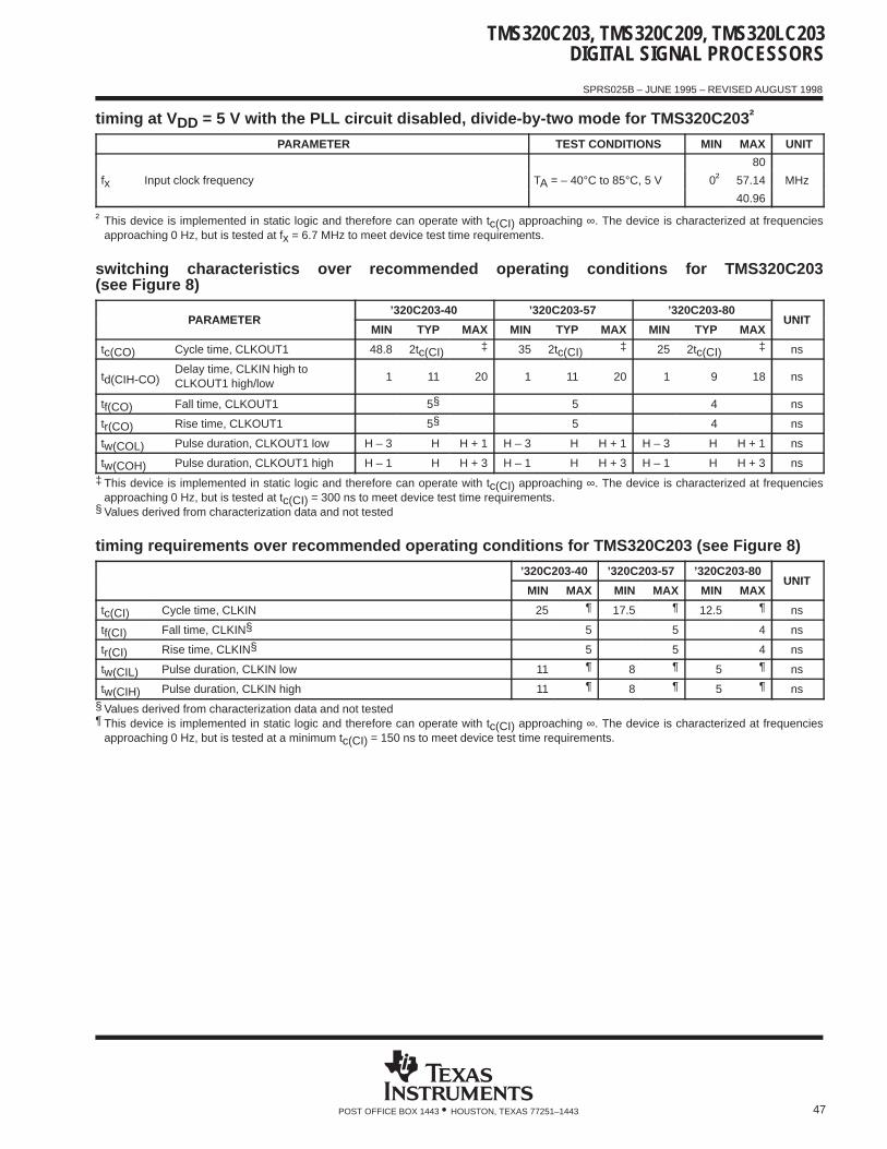
TMS320C203, TMS320C209, TMS320LC203DIGITAL SIGNAL PROCESSORS
SPRS025B – JUNE 1995 – REVISED AUGUST 1998
47POST OFFICE BOX 1443 • HOUSTON, TEXAS 77251–1443
timing at V DD = 5 V with the PLL circuit disabled, divide-by-two mode for TMS320C203 †
PARAMETER TEST CONDITIONS MIN MAX UNIT
†80
fx Input clock frequency TA = – 40°C to 85°C, 5 V 0† 57.14 MHz
40.96
† This device is implemented in static logic and therefore can operate with tc(CI) approaching ∞. The device is characterized at frequenciesapproaching 0 Hz, but is tested at fx = 6.7 MHz to meet device test time requirements.
switching characteristics over recommended operating conditions for TMS320C203(see Figure 8)
PARAMETER’320C203-40 ’320C203-57 ’320C203-80
UNITPARAMETERMIN TYP MAX MIN TYP MAX MIN TYP MAX
UNIT
tc(CO) Cycle time, CLKOUT1 48.8 2tc(CI) ‡ 35 2tc(CI) ‡ 25 2tc(CI) ‡ ns
td(CIH-CO)Delay time, CLKIN high toCLKOUT1 high/low
1 11 20 1 11 20 1 9 18 ns
tf(CO) Fall time, CLKOUT1 5§ 5 4 ns
tr(CO) Rise time, CLKOUT1 5§ 5 4 ns
tw(COL) Pulse duration, CLKOUT1 low H – 3 H H + 1 H – 3 H H + 1 H – 3 H H + 1 ns
tw(COH) Pulse duration, CLKOUT1 high H – 1 H H + 3 H – 1 H H + 3 H – 1 H H + 3 ns
‡ This device is implemented in static logic and therefore can operate with tc(CI) approaching ∞. The device is characterized at frequenciesapproaching 0 Hz, but is tested at tc(CI) = 300 ns to meet device test time requirements.
§ Values derived from characterization data and not tested
timing requirements over recommended operating conditions for TMS320C203 (see Figure 8)
’320C203-40 ’320C203-57 ’320C203-80UNIT
MIN MAX MIN MAX MIN MAXUNIT
tc(CI) Cycle time, CLKIN 25 ¶ 17.5 ¶ 12.5 ¶ ns
tf(CI) Fall time, CLKIN§ 5 5 4 ns
tr(CI) Rise time, CLKIN§ 5 5 4 ns
tw(CIL) Pulse duration, CLKIN low 11 ¶ 8 ¶ 5 ¶ ns
tw(CIH) Pulse duration, CLKIN high 11 ¶ 8 ¶ 5 ¶ ns
§ Values derived from characterization data and not tested¶ This device is implemented in static logic and therefore can operate with tc(CI) approaching ∞. The device is characterized at frequencies
approaching 0 Hz, but is tested at a minimum tc(CI) = 150 ns to meet device test time requirements.

TMS320C203, TMS320C209, TMS320LC203DIGITAL SIGNAL PROCESSORS
SPRS025B – JUNE 1995 – REVISED AUGUST 1998
48 POST OFFICE BOX 1443 • HOUSTON, TEXAS 77251–1443
timing at V DD = 3.3 V with the PLL circuit disabled, divide-by-two mode for TMS320LC203 †
ÁÁÁÁÁÁÁÁ
ÁÁÁÁÁÁÁÁÁÁÁÁÁÁÁÁÁÁÁÁÁÁÁÁÁÁÁÁÁÁÁÁÁÁÁÁ
PARAMETER ÁÁÁÁÁÁÁÁÁÁÁÁÁÁÁÁ
TEST CONDITIONS ÁÁÁÁÁÁ
MINÁÁÁÁÁÁ
MAXÁÁÁÁÁÁ
UNIT
ÁÁÁÁÁÁÁÁ
fx ÁÁÁÁÁÁÁÁÁÁÁÁÁÁÁÁÁÁÁÁÁÁÁÁÁÁÁÁÁÁÁÁÁÁÁÁ
Input clock frequency ÁÁÁÁÁÁÁÁÁÁÁÁÁÁÁÁ
TA = –40°C to 85°C, 3.3 VÁÁÁÁÁÁ
0†ÁÁÁÁÁÁ
40ÁÁÁÁÁÁ
MHz
† This device is implemented in static logic and therefore can operate with tc(CI) approaching ∞. The device is characterized at frequenciesapproaching 0 Hz, but is tested at fx = 6.7 MHz to meet device test time requirements.
switching characteristics over recommended operating conditions for TMS320LC203(see Figure 8)
PARAMETER’320LC203-40
UNITPARAMETERMIN TYP MAX
UNIT
tc(CO) Cycle time, CLKOUT1 50 2tc(CI) ‡ ns
td(CIH-CO) Delay time, CLKIN high to CLKOUT1 high/low 1 11 20 ns
tf(CO) Fall time, CLKOUT1§ 5 ns
tr(CO) Rise time, CLKOUT1§ 5 ns
tw(COL) Pulse duration, CLKOUT1 low H – 3 H H + 1 ns
tw(COH) Pulse duration, CLKOUT1 high H – 1 H H + 3 ns
‡ This device is implemented in static logic and therefore can operate with tc(CI) approaching ∞. The device is characterized at frequenciesapproaching 0 Hz, but is tested at tc(CI) = 300 ns to meet device test time requirements.
§ Values derived from characterization data and not tested
timing requirements over recommended operating conditions for TMS320LC203 (see Figure 8)
’320LC203-40UNIT
MIN MAXUNIT
tc(CI) Cycle time, CLKIN 25 ns
tf(CI) Fall time, CLKIN§ 5 ns
tr(CI) Rise time, CLKIN§ 5 ns
tw(CIL) Pulse duration, CLKIN low§ 9 ns
tw(CIH) Pulse duration, CLKIN high§ 9 ns
§ Values derived from characterization data and not tested
CLKOUT1
CLKIN
tw(CIL)
tf(CI)
tw(CIH)
td(CIH-CO)
tf(CO)tr(CO)
tc(CI)
tc(CO)
tw(COL)tw(COH)
tr(CI)
Figure 8. CLKIN-to-CLKOUT1 Timing Without PLL (using ÷2 clock option) for TMS320C203/LC203
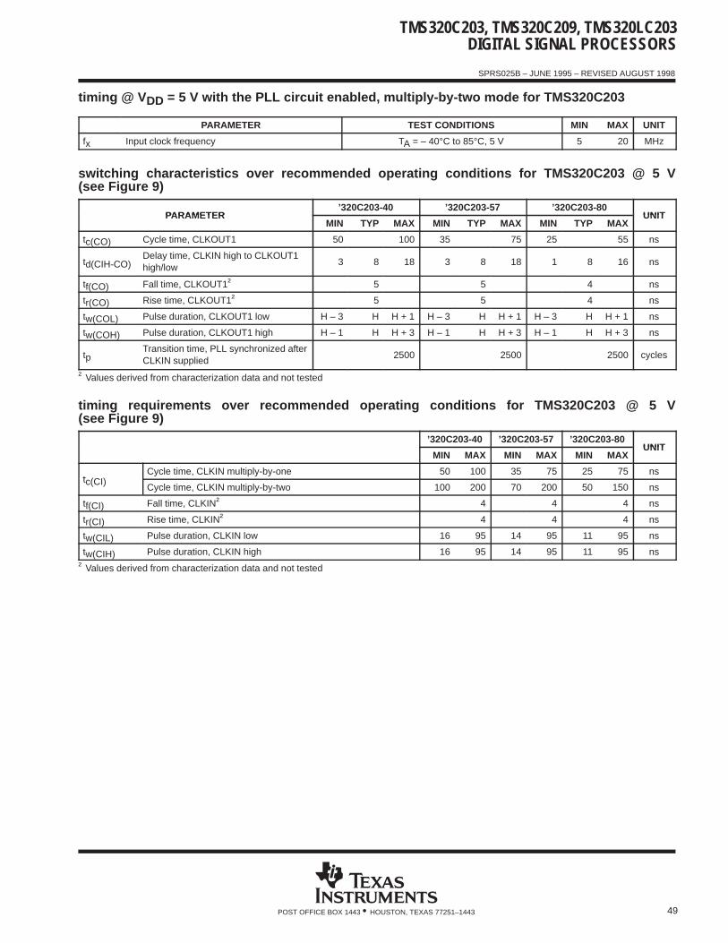
TMS320C203, TMS320C209, TMS320LC203DIGITAL SIGNAL PROCESSORS
SPRS025B – JUNE 1995 – REVISED AUGUST 1998
49POST OFFICE BOX 1443 • HOUSTON, TEXAS 77251–1443
timing @ V DD = 5 V with the PLL circuit enabled, multiply-by-two mode for TMS320C203
PARAMETER TEST CONDITIONS MIN MAX UNIT
fx Input clock frequency TA = – 40°C to 85°C, 5 V 5 20 MHz
switching characteristics over recommended operating conditions for TMS320C203 @ 5 V(see Figure 9)
PARAMETER’320C203-40 ’320C203-57 ’320C203-80
UNITPARAMETERMIN TYP MAX MIN TYP MAX MIN TYP MAX
UNIT
tc(CO) Cycle time, CLKOUT1 50 100 35 75 25 55 ns
td(CIH-CO)Delay time, CLKIN high to CLKOUT1high/low
3 8 18 3 8 18 1 8 16 ns
tf(CO) Fall time, CLKOUT1† 5 5 4 ns
tr(CO) Rise time, CLKOUT1† 5 5 4 ns
tw(COL) Pulse duration, CLKOUT1 low H – 3 H H + 1 H – 3 H H + 1 H – 3 H H + 1 ns
tw(COH) Pulse duration, CLKOUT1 high H – 1 H H + 3 H – 1 H H + 3 H – 1 H H + 3 ns
tpTransition time, PLL synchronized afterCLKIN supplied
2500 2500 2500 cycles
† Values derived from characterization data and not tested
timing requirements over recommended operating conditions for TMS320C203 @ 5 V(see Figure 9)
’320C203-40 ’320C203-57 ’320C203-80UNIT
MIN MAX MIN MAX MIN MAXUNIT
t (CI)Cycle time, CLKIN multiply-by-one 50 100 35 75 25 75 ns
tc(CI)Cycle time, CLKIN multiply-by-two 100 200 70 200 50 150 ns
tf(CI) Fall time, CLKIN† 4 4 4 ns
tr(CI) Rise time, CLKIN† 4 4 4 ns
tw(CIL) Pulse duration, CLKIN low 16 95 14 95 11 95 ns
tw(CIH) Pulse duration, CLKIN high 16 95 14 95 11 95 ns
† Values derived from characterization data and not tested

TMS320C203, TMS320C209, TMS320LC203DIGITAL SIGNAL PROCESSORS
SPRS025B – JUNE 1995 – REVISED AUGUST 1998
50 POST OFFICE BOX 1443 • HOUSTON, TEXAS 77251–1443
timing @ V DD = 3.3 V with the PLL circuit enabled, multiply-by-two mode for TMS320LC203
PARAMETER TEST CONDITIONS MIN MAX UNIT
fx Input clock frequency TA = – 40°C to 85°C, 3.3 V 5 10 MHz
switching characteristics over recommended operating conditions for TMS320LC203 @ 3.3 V(see Figure 9)
PARAMETER’320LC203-40
UNITPARAMETERMIN TYP MAX
UNIT
tc(CO) Cycle time, CLKOUT1 50 2tc(CI) 75 ns
td(CIH-CO) Delay time, CLKIN high to CLKOUT1 high/low 3 8 18 ns
tf(CO) Fall time, CLKOUT1† 5 ns
tr(CO) Rise time, CLKOUT1† 5 ns
tw(COL) Pulse duration, CLKOUT1 low H – 3 H H + 1 ns
tw(COH) Pulse duration, CLKOUT1 high H – 1 H H + 3 ns
tp Transition time, PLL synchronized after CLKIN supplied 2500 cycles
† Values derived from characterization data and not tested
timing requirements over recommended operating conditions for TMS320LC203 @ 3.3 V(see Figure 9)
’320LC203-40UNIT
MIN MAXUNIT
t (CI)Cycle time, CLKIN multiply-by-one 50 75 ns
tc(CI)Cycle time, CLKIN multiply-by-two 100 150 ns
tf(CI) Fall time, CLKIN† 5 ns
tr(CI) Rise time, CLKIN† 5 ns
tw(CIL) Pulse duration, CLKIN low 15 95 ns
tw(CIH) Pulse duration, CLKIN high 15 95 ns
† Values derived from characterization data and not tested
CLKOUT1
CLKIN
tf(CI)
tr(CI)
tr(CO)
tf(CO)
tw(COH)
td(CIH–CO)
tc(CO)
tw(CIL)
tw(CIH)
tc(CI)
tw(COL)
Figure 9. CLKIN-to-CLKOUT1 Timing With PLL (using ×2 clock option) for TMS320C203/LC203

TMS320C203, TMS320C209, TMS320LC203DIGITAL SIGNAL PROCESSORS
SPRS025B – JUNE 1995 – REVISED AUGUST 1998
51POST OFFICE BOX 1443 • HOUSTON, TEXAS 77251–1443
MEMORY AND PERIPHERAL INTERFACE TIMING FOR ’C203/’LC203
memory and parallel I/O interface read timing for TMS320C203 @ 5 V
A15–A0, PS, DS, IS, R/W, and BR timings are all included in the timings referenced to A15–A0 except whenin transition between read and write operations, where PS, DS, and IS pulse high [see tw(NSN)].
switching characteristics over recommended operating conditions [H = 0.5t c(CO)] (see Figure 10)
PARAMETERALTERNATESYMBOLS
’320C203-40’320C203-57 ’320C203-80
UNITSYMBOLSMIN MAX MIN MAX
tsu(A-RD) Setup time, address valid before RD low tsu(A)RD H – 5 H – 5 ns
th(RD-A) Hold time, address valid after RD high th(A)RD – 6 – 6 ns
td(COL-A) Delay time, CLKOUT1 low to read address valid 5 4 ns
th(COL-A)RD Hold time, read address valid after CLKOUT1 low th(A)COLRD – 4 – 3 ns
td(CO-RD) Delay time, CLKOUT1 high/low to RD low/high – 1 6 – 1 5 ns
td(COL-S) Delay time, CLKOUT1 low to STRB low/high† 0 9 0 9 ns
tw(RDL) Pulse duration, RD low (no wait states) H – 3 H + 2 H – 3 H + 2 ns
tw(RDH) Pulse duration, RD high H – 4 H + 3 H – 3 H + 3 ns
† Values derived from characterization data and not tested
timing requirements over recommended operating conditions [H = 0.5t c(CO)] (see Figure 10)
ALTERNATESYMBOLS
’320C203-40’320C203-57 ’320C203-80
UNITSYMBOLSMIN MAX MIN MAX
ta(A) Access time, from address valid to read data 2H – 15 2H – 13 ns
tsu(D-RD) Setup time, read data before RD high tsu(D)RD 13 13 ns
th(RD-D) Hold time, read data after RD high th(D)RD – 2 – 2 ns
th(AIV-D) Hold time, read data after address invalid th(D)A 0 0 ns
tsu(D-COL)RD Setup time, read data before CLKOUT1 low tsu(DCOL)RD 9 10 ns
th(COL-D)RD Hold time, read data after CLKOUT1 low th(DCOL)RD – 1 – 1 ns
ta(RD) Access time, from RD low to read data H – 12 H – 13 ns
ta(S) Access time, from STRB low to read data† 8 ns
† Values derived from characterization data and not tested

TMS320C203, TMS320C209, TMS320LC203DIGITAL SIGNAL PROCESSORS
SPRS025B – JUNE 1995 – REVISED AUGUST 1998
52 POST OFFICE BOX 1443 • HOUSTON, TEXAS 77251–1443
memory and parallel I/O interface read timing for TMS320LC203 @ 3.3 V
A15–A0, PS, DS, IS, R/W, and BR timings are all included in the timings referenced to A15–A0 except whenin transition between read and write operations, where PS, DS, and IS pulse high [see tw(NSN)].
switching characteristics over recommended operating conditions [H = 0.5t c(CO)] (see Figure 10)
PARAMETERALTERNATE ’320LC203-40
UNITPARAMETERSYMBOLS MIN MAX
UNIT
tsu(A-RD) Setup time, address valid before RD low tsu(A)RD H – 7 ns
th(RD-A) Hold time, address valid after RD high th(A)RD – 8 ns
td(COL-A) Delay time, CLKOUT1 low to read address valid 9 ns
th(COL-A)RD Hold time, read address valid after CLKOUT1 low th(A)COLRD – 4 ns
td(CO-RD) Delay time, CLKOUT1 high/low to RD low/high – 1 7 ns
td(COL-S) Delay time, CLKOUT1 low to STRB low/high† 3 16 ns
tw(RDL) Pulse duration, RD low (no wait states) H – 3 H + 2 ns
tw(RDH) Pulse duration, RD high H – 4 H + 2 ns
† Values derived from characterization data and not tested
timing requirements over recommended operating conditions [H = 0.5t c(CO)] (see Figure 10)
ALTERNATE ’320LC203-40UNIT
SYMBOLS MIN MAXUNIT
ta(A) Access time, from address valid to read data 2H – 23 ns
tsu(D-RD) Setup time, read data before RD high tsu(D)RD 22 ns
th(RD-D) Hold time, read data after RD high th(D)RD – 2 ns
th(AIV-D) Hold time, read data after address invalid th(D)A 0 ns
tsu(D-COL)RD Setup time, read data before CLKOUT1 low tsu(DCOL)RD 17 ns
th(COL-D)RD Hold time, read data after CLKOUT1 low th(DCOL)RD – 1 ns
ta(RD) Access time, from RD low to read data H – 20 ns
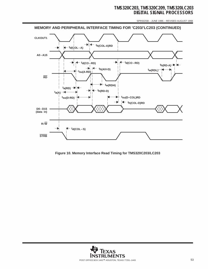
TMS320C203, TMS320C209, TMS320LC203DIGITAL SIGNAL PROCESSORS
SPRS025B – JUNE 1995 – REVISED AUGUST 1998
53POST OFFICE BOX 1443 • HOUSTON, TEXAS 77251–1443
MEMORY AND PERIPHERAL INTERFACE TIMING FOR ’C203/’LC203 (CONTINUED)
STRB
R/W
D0–D15(data in)
RD
A0–A15
CLKOUT1
tsu(D–COL)RD
th(COL-D)RD
tsu(D-RD)
th(RD-D)ta(A)
ta(RD)tw(RDH)
tw(RDL)
th(RD-A)
tsu(A-RD)
td(COL–S)
th(COL-A)RD
th(AIV-D)
td(CO–RD)td(CO–RD)
td(COL–A)
Figure 10. Memory Interface Read Timing for TMS320C203/LC203
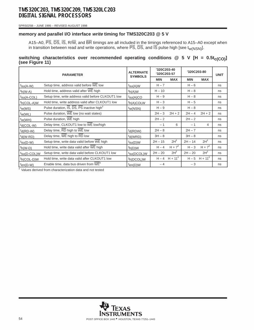
TMS320C203, TMS320C209, TMS320LC203DIGITAL SIGNAL PROCESSORS
SPRS025B – JUNE 1995 – REVISED AUGUST 1998
54 POST OFFICE BOX 1443 • HOUSTON, TEXAS 77251–1443
memory and parallel I/O interface write timing for TMS320C203 @ 5 V
A15–A0, PS, DS, IS, R/W, and BR timings are all included in the timings referenced to A15–A0 except whenin transition between read and write operations, where PS, DS, and IS pulse high [see tw(NSN)].
switching characteristics over recommended operating conditions @ 5 V [H = 0.5t c(CO)](see Figure 11)
PARAMETERALTERNATESYMBOLS
’320C203-40’320C203-57 ’320C203-80
UNITSYMBOLSMIN MAX MIN MAX
tsu(A-W) Setup time, address valid before WE low tsu(A)W H – 7 H – 6 ns
th(W-A) Hold time, address valid after WE high th(A)W H – 10 H – 8 ns
tsu(A-COL) Setup time, write address valid before CLKOUT1 low tsu(A)CO H – 9 H – 8 ns
th(COL-A)W Hold time, write address valid after CLKOUT1 low th(A)COLW H – 3 H – 5 ns
tw(MS) Pulse duration, IS, DS, PS inactive high† tw(NSN) H – 9 H – 8 ns
tw(WL) Pulse duration, WE low (no wait states) 2H – 3 2H + 2 2H – 4 2H + 2 ns
tw(WH) Pulse duration, WE high 2H – 2 2H – 2 ns
td(COL-W) Delay time, CLKOUT1 low to WE low/high – 1 6 – 1 4 ns
td(RD-W) Delay time, RD high to WE low td(RDW) 2H – 8 2H – 7 ns
td(W-RD) Delay time, WE high to RD low td(WRD) 3H – 8 3H – 8 ns
tsu(D-W) Setup time, write data valid before WE high tsu(D)W 2H – 15 2H† 2H – 14 2H† ns
th(W-D) Hold time, write data valid after WE high th(D)W H – 4 H + 7† H – 3 H + 7† ns
tsu(D-COL)W Setup time, write data valid before CLKOUT1 low tsu(DCOL)W 2H – 20 2H† 2H – 20 2H† ns
th(COL-D)W Hold time, write data valid after CLKOUT1 low th(DCOL)W H – 4 H + 11† H – 5 H + 11† ns
ten(D-W) Enable time, data bus driven from WE† ten(D)W – 4 – 3 ns
† Values derived from characterization data and not tested

TMS320C203, TMS320C209, TMS320LC203DIGITAL SIGNAL PROCESSORS
SPRS025B – JUNE 1995 – REVISED AUGUST 1998
55POST OFFICE BOX 1443 • HOUSTON, TEXAS 77251–1443
memory and parallel I/O interface write timing for TMS320LC203 @ 3.3 V
A15–A0, PS, DS, IS, R/W, and BR timings are all included in the timings referenced to A15–A0 except whenin transition between read and write operations, where PS, DS, and IS pulse high [see tw(NSN)].
switching characteristics over recommended operating conditions @ 3.3 V [H = 0.5t c(CO)](see Figure 11)
PARAMETERALTERNATE ’320LC203-40
UNITPARAMETERSYMBOLS MIN MAX
UNIT
tsu(A-W) Setup time, address valid before WE low tsu(A)W H – 5 ns
th(W-A) Hold time, address valid after WE high th(A)W H – 10 ns
tsu(A-COL) Setup time, write address valid before CLKOUT1 low tsu(A)CO H – 9 ns
th(COL-A)W Hold time, write address valid after CLKOUT1 low th(A)COLW H – 5 ns
tw(MS) Pulse duration, IS, DS, PS inactive high† tw(NSN) H – 9 ns
tw(WL) Pulse duration, WE low (no wait states) 2H – 3 2H + 1 ns
tw(WH) Pulse duration, WE high 2H – 2 ns
td(COL-W) Delay time, CLKOUT1 low to WE low/high – 1 6 ns
td(RD-W) Delay time, RD high to WE low td(RDW) 2H – 8 ns
td(W-RD) Delay time, WE high to RD low td(WRD) 3H – 8 ns
tsu(D-W) Setup time, write data valid before WE high tsu(D)W 2H – 15 2H† ns
th(W-D) Hold time, write data valid after WE high th(D)W H – 4 H + 7† ns
tsu(D-COL)W Setup time, write data valid before CLKOUT1 low tsu(DCOL)W 2H – 20 2H† ns
th(COL-D)W Hold time, write data valid after CLKOUT1 low th(DCOL)W H – 4 H + 11† ns
ten(D-W) Enable time, data bus driven from WE† ten(D)W – 4 ns
† Values derived from characterization data and not tested
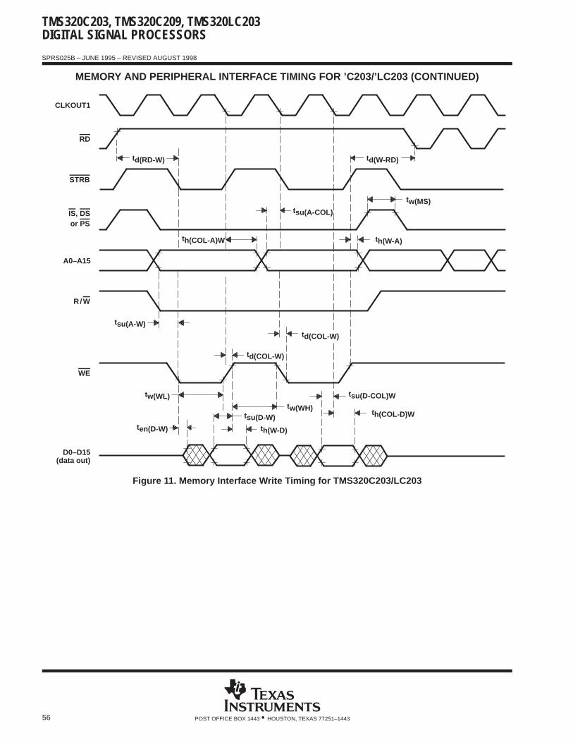
TMS320C203, TMS320C209, TMS320LC203DIGITAL SIGNAL PROCESSORS
SPRS025B – JUNE 1995 – REVISED AUGUST 1998
56 POST OFFICE BOX 1443 • HOUSTON, TEXAS 77251–1443
MEMORY AND PERIPHERAL INTERFACE TIMING FOR ’C203/’LC203 (CONTINUED)
R/W
A0–A15
or PSIS, DS
STRB
RD
CLKOUT1
th(W-A)
tsu(A-W)
tw(MS)
th(COL-A)W
tsu(A-COL)
td(RD-W) td(W-RD)
D0–D15(data out)
WE
th(W-D)
tsu(D-W)ten(D-W)
tw(WL)
td(COL-W)
tw(WH)
td(COL-W)
tsu(D-COL)W
th(COL-D)W
Figure 11. Memory Interface Write Timing for TMS320C203/LC203
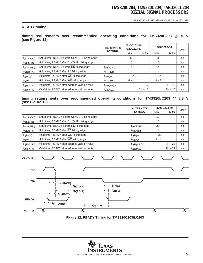
TMS320C203, TMS320C209, TMS320LC203DIGITAL SIGNAL PROCESSORS
SPRS025B – JUNE 1995 – REVISED AUGUST 1998
57POST OFFICE BOX 1443 • HOUSTON, TEXAS 77251–1443
READY timing
timing requirements over recommended operating conditions for TMS320C203 @ 5 V(see Figure 12)
ALTERNATESYMBOL
’320C203-40’320C203-57 ’320C203-80
UNITSYMBOLMIN MAX MIN MAX
tsu(R-CO) Setup time, READY before CLKOUT1 rising edge 11 11 ns
th(CO-R) Hold time, READY after CLKOUT1 rising edge 0 0 ns
tsu(R-RD) Setup time, READY before RD falling edge tsu(R)RD 14 14 ns
th(RD-R) Hold time, READY after RD falling edge th(R)RD 4 4 ns
tv(R-W) Valid time, READY after WE falling edge tv(R)W H – 14 H – 14 ns
th(W-R) Hold time, READY after WE falling edge th(R)W H + 4 H + 3 ns
tv(R-A)RD Valid time, READY after address valid on read tv(R)ARD H – 17 H – 16 ns
tv(R-A)W Valid time, READY after address valid on write tv(R)AW 2H – 18 2H – 16 ns
timing requirements over recommended operating conditions for TMS320LC203 @ 3.3 V(see Figure 12)
ALTERNATE ’320LC203-40UNIT
SYMBOL MIN MAXUNIT
tsu(R-CO) Setup time, READY before CLKOUT1 rising edge 17 ns
th(CO-R) Hold time, READY after CLKOUT1 rising edge 0 ns
tsu(R-RD) Setup time, READY before RD falling edge tsu(R)RD 22 ns
th(RD-R) Hold time, READY after RD falling edge th(R)RD 4 ns
tv(R-W) Valid time, READY after WE falling edge tv(R)W H – 23 ns
th(W-R) Hold time, READY after WE falling edge th(R)W H + 4 ns
tv(R-A)RD Valid time, READY after address valid on read tv(R)ARD H – 22 ns
tv(R-A)W Valid time, READY after address valid on write tv(R)AW 2H – 21 ns
tv(R-W)
tv(R-A)RD
tsu(R-RD)
tsu(R-CO)
A0–A15
READY
WE
RD
CLKOUT1
tv(R-A)W
th(W-R)
th(RD-R)
th(CO-R)
Figure 12. READY Timing for TMS320C203/LC203
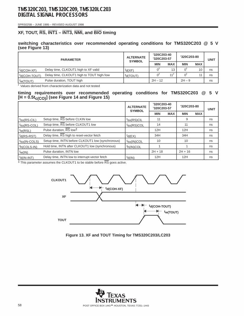
TMS320C203, TMS320C209, TMS320LC203DIGITAL SIGNAL PROCESSORS
SPRS025B – JUNE 1995 – REVISED AUGUST 1998
58 POST OFFICE BOX 1443 • HOUSTON, TEXAS 77251–1443
XF, TOUT, RS, INT1 – INT3, NMI, and BIO timing
switching characteristics over recommended operating conditions for TMS320C203 @ 5 V(see Figure 13)
PARAMETERALTERNATE
SYMBOL
’320C203-40’320C203-57 ’320C203-80
UNITSYMBOLMIN MAX MIN MAX
td(COH-XF) Delay time, CLKOUT1 high to XF valid td(XF) 0† 13 0† 10 ns
td(COH-TOUT) Delay time, CLKOUT1 high to TOUT high / low td(TOUT) 0† 11† 0† 11 ns
tw(TOUT) Pulse duration, TOUT high 2H – 12 2H – 9 ns
† Values derived from characterization data and not tested
timing requirements over recommended operating conditions for TMS320C203 @ 5 V[H = 0.5tc(CO)] (see Figure 14 and Figure 15)
ALTERNATESYMBOL
’320C203-40’320C203-57 ’320C203-80
UNITSYMBOLMIN MAX MIN MAX
tsu(RS-CIL) Setup time, RS before CLKIN low tsu(RS)CIL 11 9 ns
tsu(RS-COL) Setup time, RS before CLKOUT1 low tsu(RS)COL 14 11 ns
tw(RSL) Pulse duration, RS low‡ 12H 12H ns
td(RS-RST) Delay time, RS high to reset-vector fetch td(EX) 34H 34H ns
tsu(IN-COLS) Setup time, INTN before CLKOUT1 low (synchronous) tsu(IN)COL 10 10 ns
th(COLS-IN) Hold time, INTN after CLKOUT1 low (synchronous) th(IN)COL 1 1 ns
tw(IN) Pulse duration, INTN low 2H + 18 2H + 16 ns
td(IN-INT) Delay time, INTN low to interrupt-vector fetch td(IN) 12H 12H ns
‡ This parameter assumes the CLKOUT1 to be stable before RS goes active.
tw(TOUT)
td(COH-TOUT)
td(COH-XF)
CLKOUT1
XF
TOUT
Figure 13. XF and TOUT Timing for TMS320C203/LC203

TMS320C203, TMS320C209, TMS320LC203DIGITAL SIGNAL PROCESSORS
SPRS025B – JUNE 1995 – REVISED AUGUST 1998
59POST OFFICE BOX 1443 • HOUSTON, TEXAS 77251–1443
XF, TOUT, RS, INT1 – INT3, NMI, and BIO timing (continued)
switching characteristics over recommended operating conditions for TMS320LC203 @ 3.3 V(see Figure 13)
PARAMETERALTERNATE ’320LC203-40
UNITPARAMETERSYMBOL MIN MAX
UNIT
td(COH-XF) Delay time, CLKOUT1 high to XF valid td(XF) 0† 12 ns
td(COH-TOUT) Delay time, CLKOUT1 high to TOUT high / low td(TOUT) 0† 15 ns
tw(TOUT) Pulse duration, TOUT high 2H – 12 ns
† Values derived from characterization data and not tested
timing requirements over recommended operating conditions for TMS320LC203 @ 3.3 V[H = 0.5tc(CO)] (see Figure 14 and Figure 15)
ALTERNATE ’320LC203-40UNIT
SYMBOL MIN MAXUNIT
tsu(RS-CIL) Setup time, RS before CLKIN low tsu(RS)CIL 11 ns
tsu(RS-COL) Setup time, RS before CLKOUT1 low tsu(RS)COL 15 ns
tw(RSL) Pulse duration, RS low‡ 12H ns
td(RS-RST) Delay time, RS high to reset-vector fetch td(EX) 34H ns
tsu(IN-COLS) Setup time, INTN before CLKOUT1 low (synchronous) tsu(IN)COL 10 ns
th(COLS-IN) Hold time, INTN after CLKOUT1 low (synchronous) th(IN)COL 1 ns
tw(IN) Pulse duration, INTN low 2H + 18 ns
td(IN-INT) Delay time, INTN low to interrupt-vector fetch td(IN) 12H ns
‡ This parameter assumes the CLKOUT1 to be stable before RS goes active.
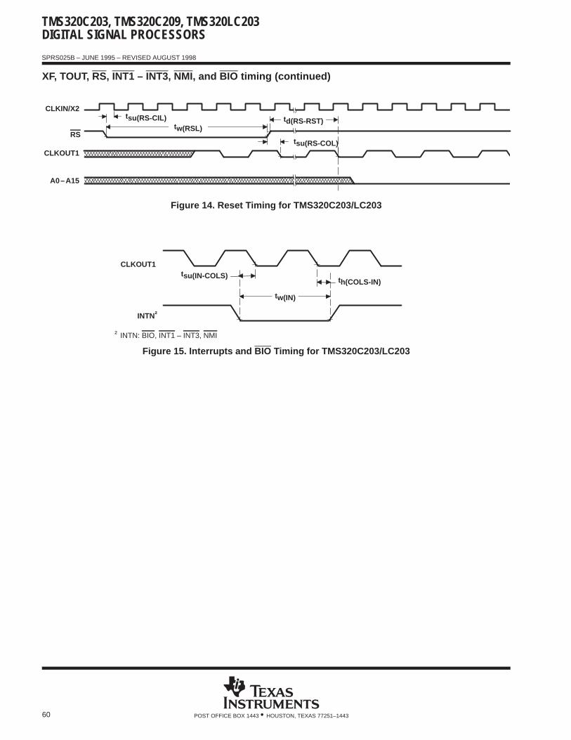
TMS320C203, TMS320C209, TMS320LC203DIGITAL SIGNAL PROCESSORS
SPRS025B – JUNE 1995 – REVISED AUGUST 1998
60 POST OFFICE BOX 1443 • HOUSTON, TEXAS 77251–1443
XF, TOUT, RS, INT1 – INT3, NMI, and BIO timing (continued)
RS
CLKIN/X2tsu(RS-CIL)
A0–A15
td(RS-RST)
CLKOUT1
tw(RSL)
tsu(RS-COL)
Figure 14. Reset Timing for TMS320C203/LC203
tsu(IN-COLS) th(COLS-IN)
CLKOUT1
INTN†
tw(IN)
† INTN: BIO, INT1 – INT3, NMI
Figure 15. Interrupts and BIO Timing for TMS320C203/LC203
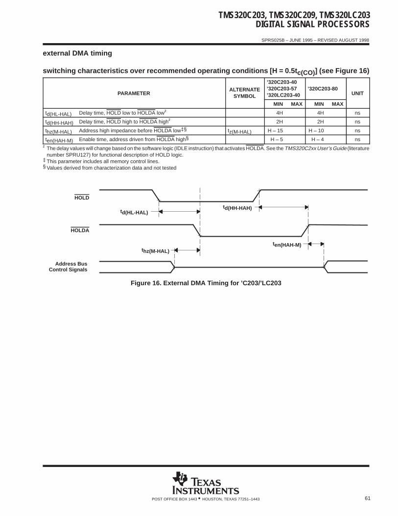
TMS320C203, TMS320C209, TMS320LC203DIGITAL SIGNAL PROCESSORS
SPRS025B – JUNE 1995 – REVISED AUGUST 1998
61POST OFFICE BOX 1443 • HOUSTON, TEXAS 77251–1443
external DMA timing
switching characteristics over recommended operating conditions [H = 0.5t c(CO)] (see Figure 16)
PARAMETERALTERNATE
SYMBOL
’320C203-40’320C203-57’320LC203-40
’320C203-80UNIT
MIN MAX MIN MAX
td(HL-HAL) Delay time, HOLD low to HOLDA low† 4H 4H ns
td(HH-HAH) Delay time, HOLD high to HOLDA high† 2H 2H ns
thz(M-HAL) Address high impedance before HOLDA lowठtz(M-HAL) H Р15 H Р10 ns
ten(HAH-M) Enable time, address driven from HOLDA high§ H – 5 H – 4 ns
† The delay values will change based on the software logic (IDLE instruction) that activates HOLDA. See the TMS320C2xx User’s Guide (literaturenumber SPRU127) for functional description of HOLD logic.
‡ This parameter includes all memory control lines.§ Values derived from characterization data and not tested
HOLDA
HOLD
Address BusControl Signals
td(HL-HAL)td(HH-HAH)
thz(M-HAL)ten(HAH-M)
Figure 16. External DMA Timing for ’C203/’LC203
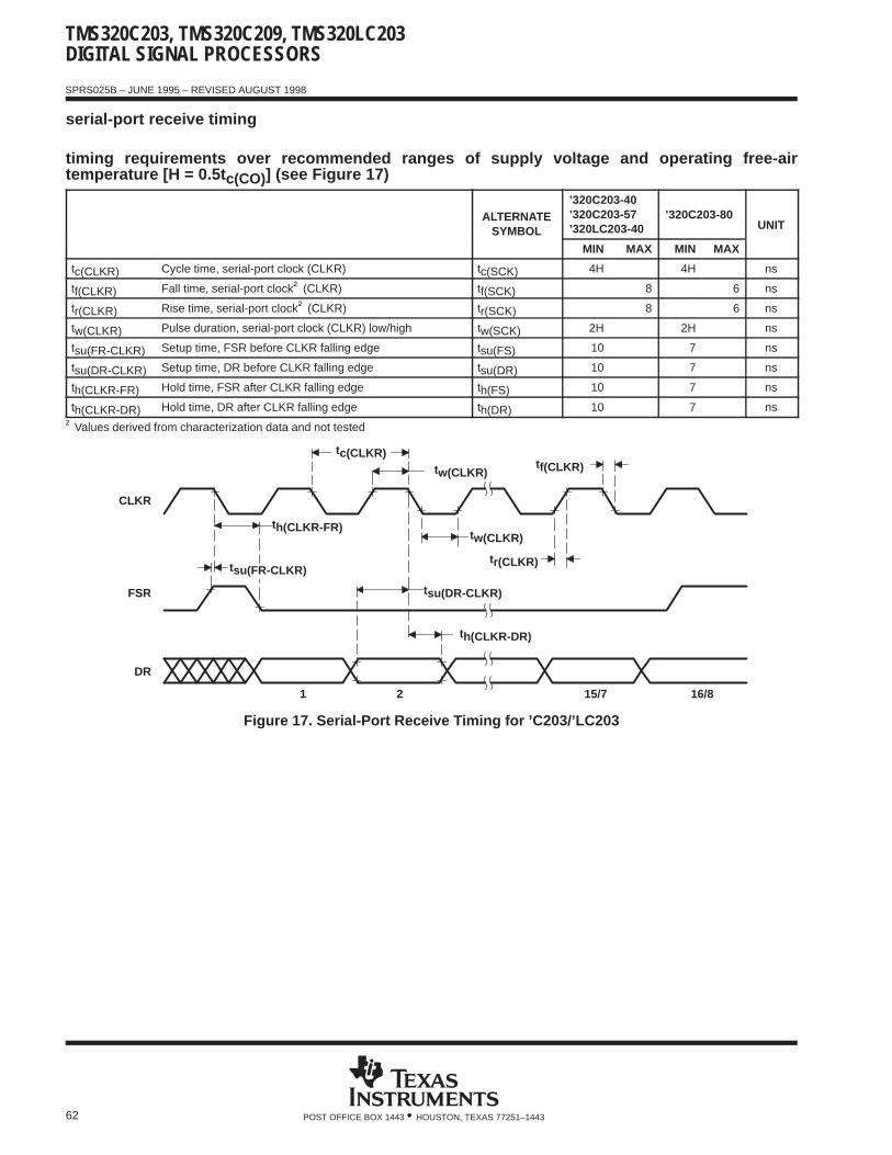
TMS320C203, TMS320C209, TMS320LC203DIGITAL SIGNAL PROCESSORS
SPRS025B – JUNE 1995 – REVISED AUGUST 1998
62 POST OFFICE BOX 1443 • HOUSTON, TEXAS 77251–1443
serial-port receive timing
timing requirements over recommended ranges of supply voltage and operating free-airtemperature [H = 0.5t c(CO)] (see Figure 17)
ALTERNATESYMBOL
’320C203-40’320C203-57’320LC203-40
’320C203-80UNIT
MIN MAX MIN MAX
tc(CLKR) Cycle time, serial-port clock (CLKR) tc(SCK) 4H 4H ns
tf(CLKR) Fall time, serial-port clock† (CLKR) tf(SCK) 8 6 ns
tr(CLKR) Rise time, serial-port clock† (CLKR) tr(SCK) 8 6 ns
tw(CLKR) Pulse duration, serial-port clock (CLKR) low/high tw(SCK) 2H 2H ns
tsu(FR-CLKR) Setup time, FSR before CLKR falling edge tsu(FS) 10 7 ns
tsu(DR-CLKR) Setup time, DR before CLKR falling edge tsu(DR) 10 7 ns
th(CLKR-FR) Hold time, FSR after CLKR falling edge th(FS) 10 7 ns
th(CLKR-DR) Hold time, DR after CLKR falling edge th(DR) 10 7 ns
† Values derived from characterization data and not tested
tsu(FR-CLKR)
CLKR
FSR
DR
1 2 15/7 16/8
th(CLKR-FR)
tw(CLKR)
tsu(DR-CLKR)
tw(CLKR)
tr(CLKR)
tf(CLKR)
th(CLKR-DR)
tc(CLKR)
Figure 17. Serial-Port Receive Timing for ’C203/’LC203
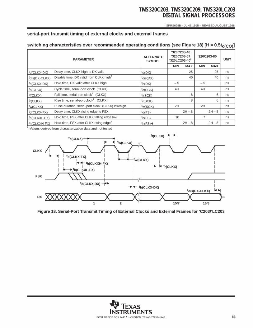
TMS320C203, TMS320C209, TMS320LC203DIGITAL SIGNAL PROCESSORS
SPRS025B – JUNE 1995 – REVISED AUGUST 1998
63POST OFFICE BOX 1443 • HOUSTON, TEXAS 77251–1443
serial-port transmit timing of external clocks and external frames
switching characteristics over recommended operating conditions (see Figure 18) [H = 0.5t c(CO)]
PARAMETERALTERNATE
SYMBOL
’320C203-40’320C203-57
’320LC203-40†’320C203-80
UNIT
MIN MAX MIN MAX
td(CLKX-DX) Delay time, CLKX high to DX valid td(DX) 25 25 ns
tdis(DX-CLKX) Disable time, DX valid from CLKX high† tdis(DX) 40 40 ns
th(CLKX-DX) Hold time, DX valid after CLKX high th(DX) – 5 – 5 ns
tc(CLKX) Cycle time, serial-port clock (CLKX) tc(SCK) 4H 4H ns
tf(CLKX) Fall time, serial-port clock† (CLKX) tf(SCK) 8 6 ns
tr(CLKX) Rise time, serial-port clock† (CLKX) tr(SCK) 8 6 ns
tw(CLKX) Pulse duration, serial-port clock (CLKX) low/high tw(SCK) 2H 2H ns
td(CLKX-FX) Delay time, CLKX rising edge to FSX td(FS) 2H – 8 2H – 8 ns
th(CLKXL-FX) Hold time, FSX after CLKX falling edge low th(FS) 10 7 ns
th(CLKXH-FX) Hold time, FSX after CLKX rising edge† th(FS)H 2H – 8 2H – 8 ns
† Values derived from characterization data and not tested
CLKX
FSX
DX
td(CLKX-FX)
th(CLKXH-FX)
tw(CLKX)
tw(CLKX)
tc(CLKX)
tr(CLKX)
tf(CLKX)
td(CLKX-DX)th(CLKX-DX)
tdis(DX-CLKX)
1 2 15/7 16/8
th(CLKXL-FX)
Figure 18. Serial-Port Transmit Timing of External Clocks and External Frames for ’C203/’LC203
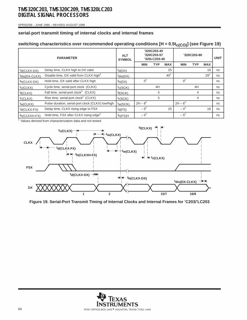
TMS320C203, TMS320C209, TMS320LC203DIGITAL SIGNAL PROCESSORS
SPRS025B – JUNE 1995 – REVISED AUGUST 1998
64 POST OFFICE BOX 1443 • HOUSTON, TEXAS 77251–1443
serial-port transmit timing of internal clocks and internal frames
switching characteristics over recommended operating conditions [H = 0.5t c(CO)] (see Figure 19)
PARAMETERALT
SYMBOL
’320C203-40’320C203-57’320LC203-40
’320C203-80UNIT
MIN TYP MAX MIN TYP MAX
td(CLKX-DX) Delay time, CLKX high to DX valid td(DX) 25 18 ns
tdis(DX-CLKX) Disable time, DX valid from CLKX high† tdis(DX) 40† 29† ns
th(CLKX-DX) Hold time, DX valid after CLKX high th(DX) 0† 0† ns
tc(CLKX) Cycle time, serial-port clock (CLKX) tc(SCK) 4H 4H ns
tf(CLKX) Fall time, serial-port clock† (CLKX) tf(SCK) 5 4 ns
tr(CLKX) Rise time, serial-port clock† (CLKX) tr(SCK) 5 4 ns
tw(CLKX) Pulse duration, serial-port clock (CLKX) low/high tw(SCK) 2H – 8† 2H – 6† ns
td(CLKX-FX) Delay time, CLKX rising edge to FSX td(FS) – 5† 25 – 4† 18 ns
th(CLKXH-FX) Hold time, FSX after CLKX rising edge† th(FS)H – 5† – 5† ns
† Values derived from characterization data and not tested
CLKX
FSX
DX
td(CLKX-FX)
th(CLKXH-FX)
tw(CLKX)
tw(CLKX)
tc(CLKX)
tr(CLKX)
tf(CLKX)
td(CLKX-DX)th(CLKX-DX)
tdis(DX-CLKX)
1 2 15/7 16/8
Figure 19. Serial-Port Transmit Timing of Internal Clocks and Internal Frames for ’C203/’LC203

TMS320C203, TMS320C209, TMS320LC203DIGITAL SIGNAL PROCESSORS
SPRS025B – JUNE 1995 – REVISED AUGUST 1998
65POST OFFICE BOX 1443 • HOUSTON, TEXAS 77251–1443
absolute maximum ratings over case temperature range (unless otherwise noted) (’320C209 only) †
Supply voltage range, VDD (see Note 1) – 0.3 V to 7 V. . . . . . . . . . . . . . . . . . . . . . . . . . . . . . . . . . . . . . . . . . . . . . Input voltage range – 0.3 V to 7 V. . . . . . . . . . . . . . . . . . . . . . . . . . . . . . . . . . . . . . . . . . . . . . . . . . . . . . . . . . . . . . . . Output voltage range – 0.3 V to 7 V. . . . . . . . . . . . . . . . . . . . . . . . . . . . . . . . . . . . . . . . . . . . . . . . . . . . . . . . . . . . . . . Operating free-air temperature range, TC 0°C to 85°C. . . . . . . . . . . . . . . . . . . . . . . . . . . . . . . . . . . . . . . . . . . . . . Storage temperature range, Tstg – 55°C to 150°C. . . . . . . . . . . . . . . . . . . . . . . . . . . . . . . . . . . . . . . . . . . . . . . . . .
† Stresses beyond those listed under “absolute maximum ratings” may cause permanent damage to the device. These are stress ratings only, andfunctional operation of the device at these or any other conditions beyond those indicated under “recommended operating conditions” is notimplied. Exposure to absolute-maximum-rated conditions for extended periods may affect device reliability.
NOTE 1: All voltage values are with respect to VSS.
recommended operating conditions for TMS320C209 @ 5 V
TEST CONDITIONS MIN NOM MAX UNIT
VDD Supply voltage 5-V operation 4.5 5 5.5 V
VSS Supply voltage 0 V
CLKIN/X2 3 VDD + 0 3VIH High-level input voltage
CLKIN/X2 3 VDD + 0.3VVIH High-level in ut voltage
Inputs 2.0 VDD + 0.3V
CLKIN/X2 – 0.3 0.7
VIL Low-level input voltage RS 0.8 V
All other inputs – 0.3 0.8
IOH High-level output current – 300 µA
IOL Low-level output current 2 mA
TC Case temperature 0 85 °C
electrical characteristics over recommended ranges of supply voltage and operating casetemperature for TMS320C209 @ 5 V
PARAMETER TEST CONDITIONS MIN TYP MAX UNIT
VOH High-level output voltage 5-V operation, IOH = MAX 2.4 V
VOL Low-level output voltage 5-V operation, IOL = MAX 0.6 V
II Input current VI = VDD or 0 V – 10 10 µA
IOZ Output current, high-impedance state (off-state) VO = VDD or 0 V ± 5 µA
IDD Supply current, core CPU 5-V operation, 57 MHz 76 mA
Ci Input capacitance 15 pF
Co Output capacitance 15 pF
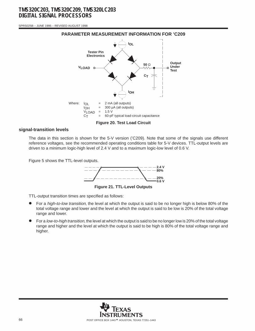
TMS320C203, TMS320C209, TMS320LC203DIGITAL SIGNAL PROCESSORS
SPRS025B – JUNE 1995 – REVISED AUGUST 1998
66 POST OFFICE BOX 1443 • HOUSTON, TEXAS 77251–1443
PARAMETER MEASUREMENT INFORMATION FOR ’C209
Tester PinElectronics
VLOAD
IOL
CT
IOH
OutputUnderTest
50 Ω
Where: IOL = 2 mA (all outputs)IOH = 300 µA (all outputs)VLOAD = 1.5 VCT = 60-pF typical load-circuit capacitance
Figure 20. Test Load Circuit
signal-transition levels
The data in this section is shown for the 5-V version (’C209). Note that some of the signals use differentreference voltages, see the recommended operating conditions table for 5-V devices. TTL-output levels aredriven to a minimum logic-high level of 2.4 V and to a maximum logic-low level of 0.6 V.
Figure 5 shows the TTL-level outputs.
0.6 V20%
2.4 V 80%
Figure 21. TTL-Level Outputs
TTL-output transition times are specified as follows:
For a high-to-low transition, the level at which the output is said to be no longer high is below 80% of thetotal voltage range and lower and the level at which the output is said to be low is 20% of the total voltagerange and lower.
For a low-to-high transition, the level at which the output is said to be no longer low is 20% of the total voltagerange and higher and the level at which the output is said to be high is 80% of the total voltage range andhigher.
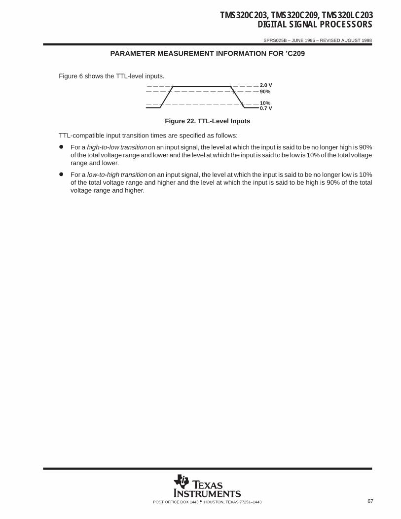
TMS320C203, TMS320C209, TMS320LC203DIGITAL SIGNAL PROCESSORS
SPRS025B – JUNE 1995 – REVISED AUGUST 1998
67POST OFFICE BOX 1443 • HOUSTON, TEXAS 77251–1443
PARAMETER MEASUREMENT INFORMATION FOR ’C209
Figure 6 shows the TTL-level inputs.
0.7 V10%
2.0 V90%
Figure 22. TTL-Level Inputs
TTL-compatible input transition times are specified as follows:
For a high-to-low transition on an input signal, the level at which the input is said to be no longer high is 90%of the total voltage range and lower and the level at which the input is said to be low is 10% of the total voltagerange and lower.
For a low-to-high transition on an input signal, the level at which the input is said to be no longer low is 10%of the total voltage range and higher and the level at which the input is said to be high is 90% of the totalvoltage range and higher.

TMS320C203, TMS320C209, TMS320LC203DIGITAL SIGNAL PROCESSORS
SPRS025B – JUNE 1995 – REVISED AUGUST 1998
68 POST OFFICE BOX 1443 • HOUSTON, TEXAS 77251–1443
PARAMETER MEASUREMENT INFORMATION FOR ’C209
timing parameter symbology
Timing parameter symbols used are created in accordance with JEDEC Standard 100-A. To shorten thesymbols, some of the pin names and other related terminology have been abbreviated as follows:
A Address or A[15:0] R READY
CI CLKIN/X2 RD Read cycle or RD
CO CLKOUT1 RS RESET pins RS or RS
D Data or D[15:0] S STRB
FS FSX SCK Serial-port clock
IN INTN; BIO, INT1–INT3, NMI W Write cycle or WE
MS Memory strobe pins IS, DS, or PS
Lowercase subscripts and their meanings are: The following letters and symbols and their meanings are:
a access time H High
c cycle time (period) L Low
d delay time V Valid
dis disable time Z High impedance
en enable time X Unknown, changing, or don’t care level
f fall time
h hold time
r rise time
su setup time
t transition time
v valid time
w pulse duration (width)
general notes on timing parameters for ’C209
All output signals from the TMS320C2xx devices (including CLKOUT1) are derived from an internal clock suchthat all output transitions for a given half cycle occur with a minimum of skewing relative to each other.
The signal combinations shown in the following timing diagrams may not necessarily represent actual cycles.For actual cycle examples, refer to the appropriate cycle description section of this data sheet.
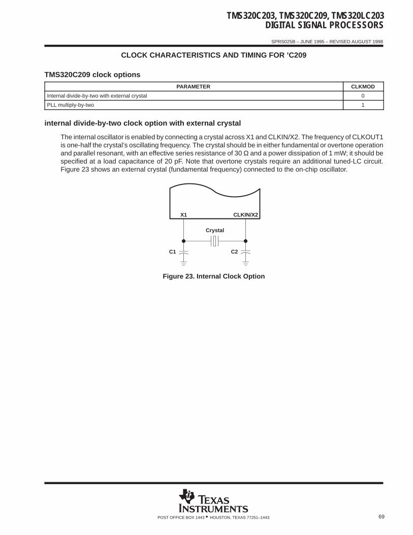
TMS320C203, TMS320C209, TMS320LC203DIGITAL SIGNAL PROCESSORS
SPRS025B – JUNE 1995 – REVISED AUGUST 1998
69POST OFFICE BOX 1443 • HOUSTON, TEXAS 77251–1443
CLOCK CHARACTERISTICS AND TIMING FOR ’C209
TMS320C209 clock options
PARAMETER CLKMOD
Internal divide-by-two with external crystal 0
PLL multiply-by-two 1
internal divide-by-two clock option with external crystal
The internal oscillator is enabled by connecting a crystal across X1 and CLKIN/X2. The frequency of CLKOUT1is one-half the crystal’s oscillating frequency. The crystal should be in either fundamental or overtone operationand parallel resonant, with an effective series resistance of 30 Ω and a power dissipation of 1 mW; it should bespecified at a load capacitance of 20 pF. Note that overtone crystals require an additional tuned-LC circuit.Figure 23 shows an external crystal (fundamental frequency) connected to the on-chip oscillator.
X1 CLKIN/X2
C1 C2
Crystal
Figure 23. Internal Clock Option
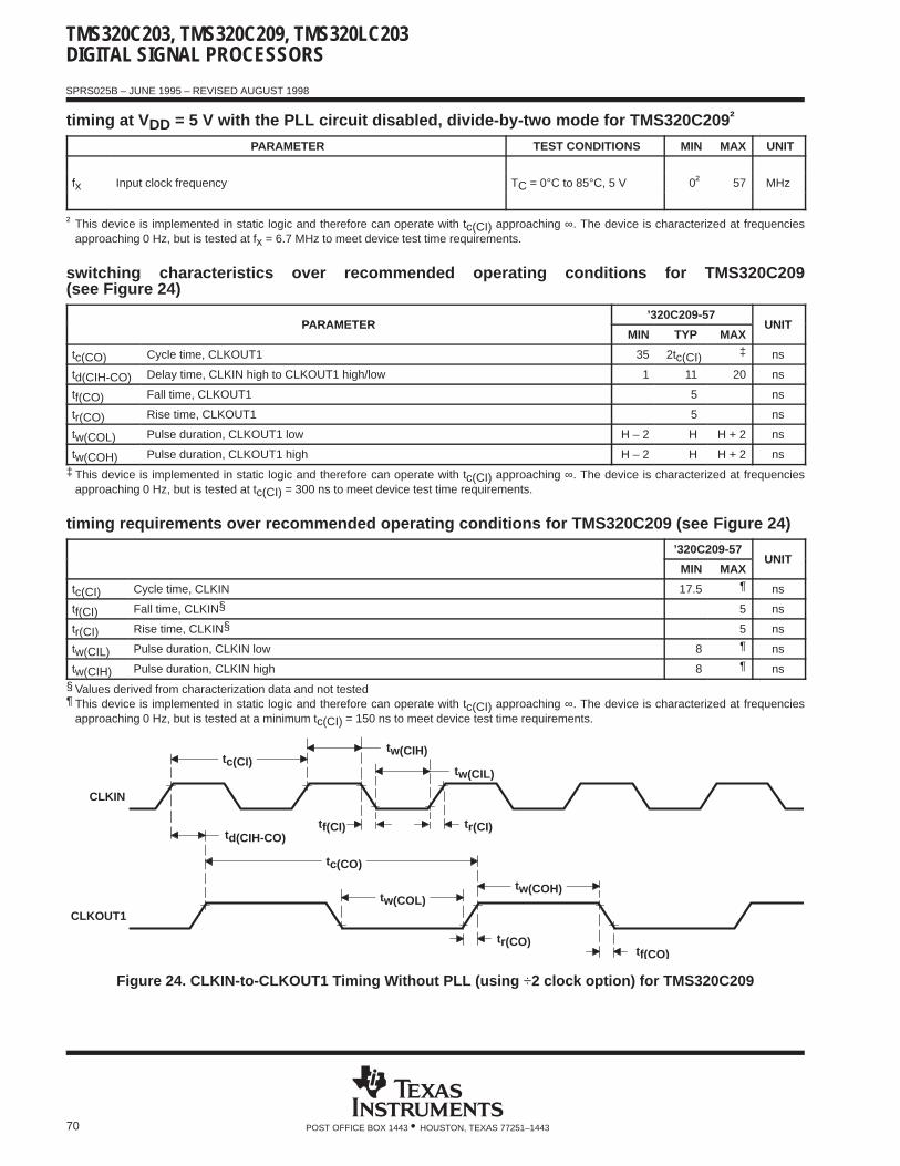
TMS320C203, TMS320C209, TMS320LC203DIGITAL SIGNAL PROCESSORS
SPRS025B – JUNE 1995 – REVISED AUGUST 1998
70 POST OFFICE BOX 1443 • HOUSTON, TEXAS 77251–1443
timing at V DD = 5 V with the PLL circuit disabled, divide-by-two mode for TMS320C209 †
PARAMETER TEST CONDITIONS MIN MAX UNIT
†fx Input clock frequency TC = 0°C to 85°C, 5 V 0† 57 MHz
† This device is implemented in static logic and therefore can operate with tc(CI) approaching ∞. The device is characterized at frequenciesapproaching 0 Hz, but is tested at fx = 6.7 MHz to meet device test time requirements.
switching characteristics over recommended operating conditions for TMS320C209(see Figure 24)
PARAMETER’320C209-57
UNITPARAMETERMIN TYP MAX
UNIT
tc(CO) Cycle time, CLKOUT1 35 2tc(CI) ‡ ns
td(CIH-CO) Delay time, CLKIN high to CLKOUT1 high/low 1 11 20 ns
tf(CO) Fall time, CLKOUT1 5 ns
tr(CO) Rise time, CLKOUT1 5 ns
tw(COL) Pulse duration, CLKOUT1 low H – 2 H H + 2 ns
tw(COH) Pulse duration, CLKOUT1 high H – 2 H H + 2 ns
‡ This device is implemented in static logic and therefore can operate with tc(CI) approaching ∞. The device is characterized at frequenciesapproaching 0 Hz, but is tested at tc(CI) = 300 ns to meet device test time requirements.
timing requirements over recommended operating conditions for TMS320C209 (see Figure 24)
’320C209-57UNIT
MIN MAXUNIT
tc(CI) Cycle time, CLKIN 17.5 ¶ ns
tf(CI) Fall time, CLKIN§ 5 ns
tr(CI) Rise time, CLKIN§ 5 ns
tw(CIL) Pulse duration, CLKIN low 8 ¶ ns
tw(CIH) Pulse duration, CLKIN high 8 ¶ ns
§ Values derived from characterization data and not tested¶ This device is implemented in static logic and therefore can operate with tc(CI) approaching ∞. The device is characterized at frequencies
approaching 0 Hz, but is tested at a minimum tc(CI) = 150 ns to meet device test time requirements.
CLKOUT1
CLKIN
tw(CIL)
tf(CI)
tw(CIH)
td(CIH-CO)
tf(CO)tr(CO)
tc(CI)
tc(CO)
tw(COL)tw(COH)
tr(CI)
Figure 24. CLKIN-to-CLKOUT1 Timing Without PLL (using ÷2 clock option) for TMS320C209
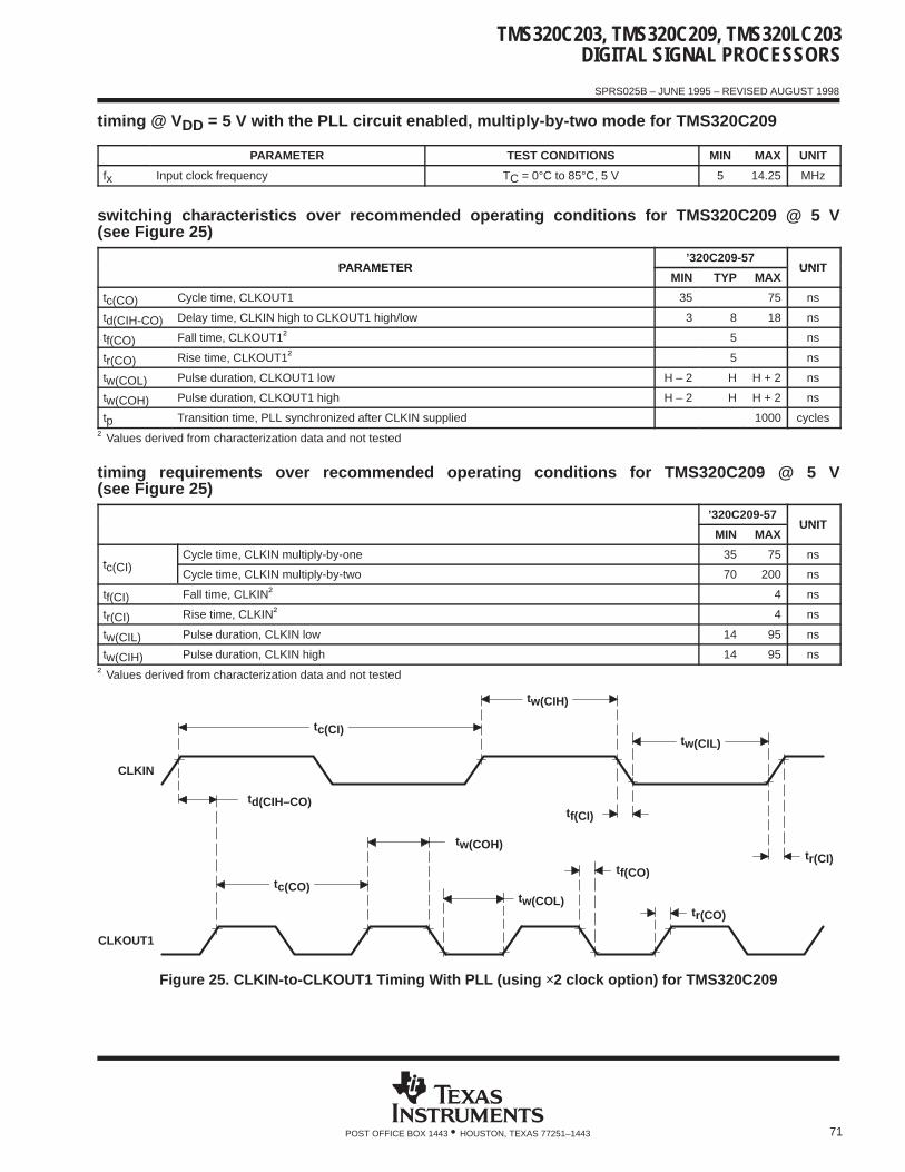
TMS320C203, TMS320C209, TMS320LC203DIGITAL SIGNAL PROCESSORS
SPRS025B – JUNE 1995 – REVISED AUGUST 1998
71POST OFFICE BOX 1443 • HOUSTON, TEXAS 77251–1443
timing @ V DD = 5 V with the PLL circuit enabled, multiply-by-two mode for TMS320C209
PARAMETER TEST CONDITIONS MIN MAX UNIT
fx Input clock frequency TC = 0°C to 85°C, 5 V 5 14.25 MHz
switching characteristics over recommended operating conditions for TMS320C209 @ 5 V(see Figure 25)
PARAMETER’320C209-57
UNITPARAMETERMIN TYP MAX
UNIT
tc(CO) Cycle time, CLKOUT1 35 75 ns
td(CIH-CO) Delay time, CLKIN high to CLKOUT1 high/low 3 8 18 ns
tf(CO) Fall time, CLKOUT1† 5 ns
tr(CO) Rise time, CLKOUT1† 5 ns
tw(COL) Pulse duration, CLKOUT1 low H – 2 H H + 2 ns
tw(COH) Pulse duration, CLKOUT1 high H – 2 H H + 2 ns
tp Transition time, PLL synchronized after CLKIN supplied 1000 cycles
† Values derived from characterization data and not tested
timing requirements over recommended operating conditions for TMS320C209 @ 5 V(see Figure 25)
’320C209-57UNIT
MIN MAXUNIT
t (CI)Cycle time, CLKIN multiply-by-one 35 75 ns
tc(CI)Cycle time, CLKIN multiply-by-two 70 200 ns
tf(CI) Fall time, CLKIN† 4 ns
tr(CI) Rise time, CLKIN† 4 ns
tw(CIL) Pulse duration, CLKIN low 14 95 ns
tw(CIH) Pulse duration, CLKIN high 14 95 ns
† Values derived from characterization data and not tested
CLKOUT1
CLKIN
tf(CI)
tr(CI)
tr(CO)
tf(CO)
tw(COH)
td(CIH–CO)
tc(CO)
tw(CIL)
tw(CIH)
tc(CI)
tw(COL)
Figure 25. CLKIN-to-CLKOUT1 Timing With PLL (using ×2 clock option) for TMS320C209
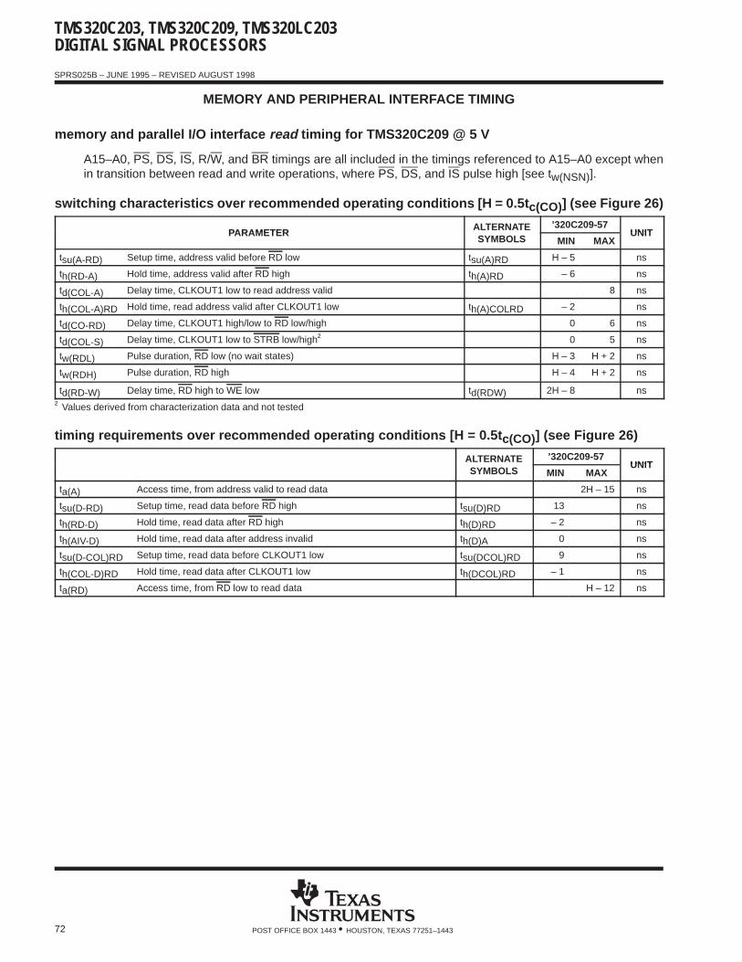
TMS320C203, TMS320C209, TMS320LC203DIGITAL SIGNAL PROCESSORS
SPRS025B – JUNE 1995 – REVISED AUGUST 1998
72 POST OFFICE BOX 1443 • HOUSTON, TEXAS 77251–1443
MEMORY AND PERIPHERAL INTERFACE TIMING
memory and parallel I/O interface read timing for TMS320C209 @ 5 V
A15–A0, PS, DS, IS, R/W, and BR timings are all included in the timings referenced to A15–A0 except whenin transition between read and write operations, where PS, DS, and IS pulse high [see tw(NSN)].
switching characteristics over recommended operating conditions [H = 0.5t c(CO)] (see Figure 26)
PARAMETERALTERNATE ’320C209-57
UNITPARAMETERSYMBOLS MIN MAX
UNIT
tsu(A-RD) Setup time, address valid before RD low tsu(A)RD H – 5 ns
th(RD-A) Hold time, address valid after RD high th(A)RD – 6 ns
td(COL-A) Delay time, CLKOUT1 low to read address valid 8 ns
th(COL-A)RD Hold time, read address valid after CLKOUT1 low th(A)COLRD – 2 ns
td(CO-RD) Delay time, CLKOUT1 high/low to RD low/high 0 6 ns
td(COL-S) Delay time, CLKOUT1 low to STRB low/high† 0 5 ns
tw(RDL) Pulse duration, RD low (no wait states) H – 3 H + 2 ns
tw(RDH) Pulse duration, RD high H – 4 H + 2 ns
td(RD-W) Delay time, RD high to WE low td(RDW) 2H – 8 ns
† Values derived from characterization data and not tested
timing requirements over recommended operating conditions [H = 0.5t c(CO)] (see Figure 26)
ALTERNATE ’320C209-57UNIT
SYMBOLS MIN MAXUNIT
ta(A) Access time, from address valid to read data 2H – 15 ns
tsu(D-RD) Setup time, read data before RD high tsu(D)RD 13 ns
th(RD-D) Hold time, read data after RD high th(D)RD – 2 ns
th(AIV-D) Hold time, read data after address invalid th(D)A 0 ns
tsu(D-COL)RD Setup time, read data before CLKOUT1 low tsu(DCOL)RD 9 ns
th(COL-D)RD Hold time, read data after CLKOUT1 low th(DCOL)RD – 1 ns
ta(RD) Access time, from RD low to read data H – 12 ns

TMS320C203, TMS320C209, TMS320LC203DIGITAL SIGNAL PROCESSORS
SPRS025B – JUNE 1995 – REVISED AUGUST 1998
73POST OFFICE BOX 1443 • HOUSTON, TEXAS 77251–1443
memory and parallel I/O interface read timing for TMS320C209 @ 5 V (continued)
STRB
R/W
D0–D15(data in)
RD
A0–A15
CLKOUT1
tsu(D–COL)RD
th(COL-D)RD
tsu(D-RD)
th(RD-D)ta(A)
ta(RD)tw(RDH)
tw(RDL)
th(RD-A)
tsu(A-RD)
td(COL–S)
th(COL-A)RD
th(AIV-D)
td(CO–RD)td(CO–RD)
td(COL–A)
Figure 26. Memory Interface Read Timing for TMS320C209
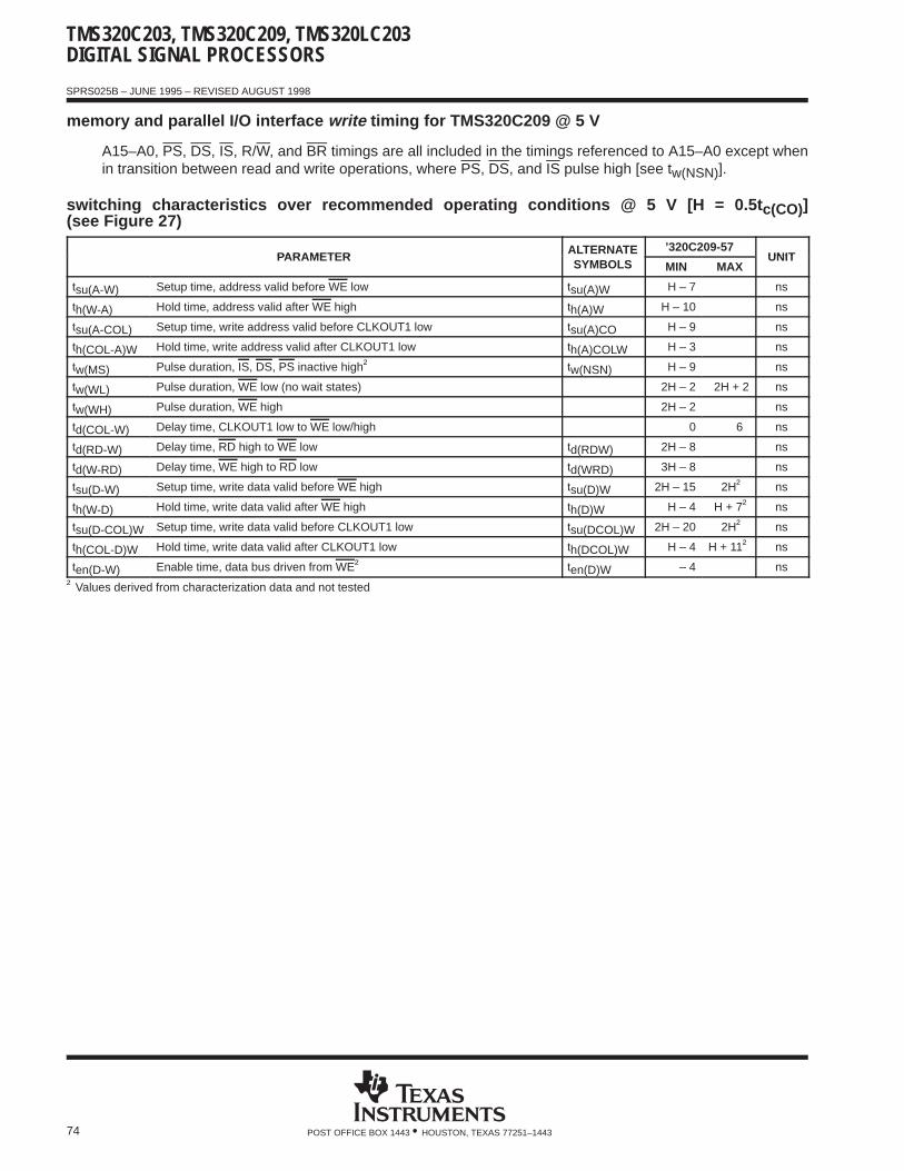
TMS320C203, TMS320C209, TMS320LC203DIGITAL SIGNAL PROCESSORS
SPRS025B – JUNE 1995 – REVISED AUGUST 1998
74 POST OFFICE BOX 1443 • HOUSTON, TEXAS 77251–1443
memory and parallel I/O interface write timing for TMS320C209 @ 5 V
A15–A0, PS, DS, IS, R/W, and BR timings are all included in the timings referenced to A15–A0 except whenin transition between read and write operations, where PS, DS, and IS pulse high [see tw(NSN)].
switching characteristics over recommended operating conditions @ 5 V [H = 0.5t c(CO)](see Figure 27)
PARAMETERALTERNATE ’320C209-57
UNITPARAMETERSYMBOLS MIN MAX
UNIT
tsu(A-W) Setup time, address valid before WE low tsu(A)W H – 7 ns
th(W-A) Hold time, address valid after WE high th(A)W H – 10 ns
tsu(A-COL) Setup time, write address valid before CLKOUT1 low tsu(A)CO H – 9 ns
th(COL-A)W Hold time, write address valid after CLKOUT1 low th(A)COLW H – 3 ns
tw(MS) Pulse duration, IS, DS, PS inactive high† tw(NSN) H – 9 ns
tw(WL) Pulse duration, WE low (no wait states) 2H – 2 2H + 2 ns
tw(WH) Pulse duration, WE high 2H – 2 ns
td(COL-W) Delay time, CLKOUT1 low to WE low/high 0 6 ns
td(RD-W) Delay time, RD high to WE low td(RDW) 2H – 8 ns
td(W-RD) Delay time, WE high to RD low td(WRD) 3H – 8 ns
tsu(D-W) Setup time, write data valid before WE high tsu(D)W 2H – 15 2H† ns
th(W-D) Hold time, write data valid after WE high th(D)W H – 4 H + 7† ns
tsu(D-COL)W Setup time, write data valid before CLKOUT1 low tsu(DCOL)W 2H – 20 2H† ns
th(COL-D)W Hold time, write data valid after CLKOUT1 low th(DCOL)W H – 4 H + 11† ns
ten(D-W) Enable time, data bus driven from WE† ten(D)W – 4 ns
† Values derived from characterization data and not tested
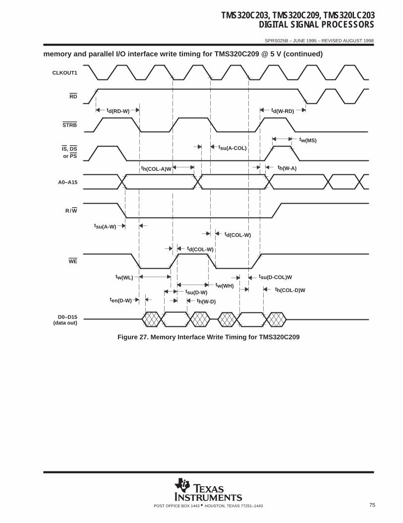
TMS320C203, TMS320C209, TMS320LC203DIGITAL SIGNAL PROCESSORS
SPRS025B – JUNE 1995 – REVISED AUGUST 1998
75POST OFFICE BOX 1443 • HOUSTON, TEXAS 77251–1443
memory and parallel I/O interface write timing for TMS320C209 @ 5 V (continued)
th(COL-A)W
R/W
A0–A15
or PSIS, DS
STRB
RD
CLKOUT1
th(W-A)
tsu(A-W)
tw(MS)tsu(A-COL)
td(RD-W) td(W-RD)
D0–D15(data out)
WE
th(W-D)
tsu(D-W)ten(D-W)
tw(WL)
td(COL-W)
tw(WH)
tsu(D-COL)W
th(COL-D)W
td(COL-W)
Figure 27. Memory Interface Write Timing for TMS320C209

TMS320C203, TMS320C209, TMS320LC203DIGITAL SIGNAL PROCESSORS
SPRS025B – JUNE 1995 – REVISED AUGUST 1998
76 POST OFFICE BOX 1443 • HOUSTON, TEXAS 77251–1443
READY timing
timing requirements over recommended operating conditions for TMS320C209 @ 5 V(see Figure 28)
ALTERNATE 320C209-57UNIT
SYMBOL MIN MAXUNIT
tsu(R-CO) Setup time, READY before CLKOUT1 rising edge 11 ns
th(CO-R) Hold time, READY after CLKOUT1 rising edge 0 ns
tsu(R-RD) Setup time, READY before RD falling edge tsu(R)RD 14 ns
th(RD-R) Hold time, READY after RD falling edge th(R)RD 4 ns
tv(R-W) Valid time, READY after WE falling edge tv(R)W H – 13 ns
th(W-R) Hold time, READY after WE falling edge th(R)W H + 4 ns
tv(R-A)RD Valid time, READY after address valid on read tv(R)ARD H – 17 ns
tv(R-A)W Valid time, READY after address valid on write tv(R)AW 2H – 18 ns
tv(R-W)
tv(R-A)RD
tsu(R-RD)
tsu(R-CO)
A0–A15
READY
WE
RD
CLKOUT1
tv(R-A)W
th(W-R)
th(RD-R)
th(CO-R)
Figure 28. READY Timing for TMS320C209

TMS320C203, TMS320C209, TMS320LC203DIGITAL SIGNAL PROCESSORS
SPRS025B – JUNE 1995 – REVISED AUGUST 1998
77POST OFFICE BOX 1443 • HOUSTON, TEXAS 77251–1443
XF, TOUT, RS, INT1 – INT3, NMI, and BIO timing
switching characteristics over recommended operating conditions for TMS320C209 @ 5 V(see Figure 29)
PARAMETERALTERNATE ’320C209-57
UNITPARAMETERSYMBOL MIN MAX
UNIT
td(COH-XF) Delay time, CLKOUT1 high to XF valid td(XF) 0† 13 ns
td(COH-TOUT) Delay time, CLKOUT1 high to TOUT high / low td(TOUT) 0† 11† ns
tw(TOUT) Pulse duration, TOUT high 2H – 12 ns
† Values derived from characterization data and not tested
tw(TOUT)
td(COH-TOUT)
td(COH-XF)
CLKOUT1
XF
TOUT
Figure 29. XF and TOUT Timing for TMS320C209
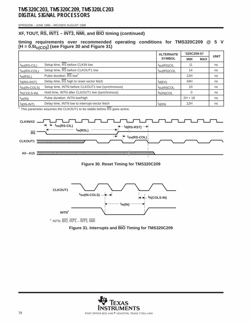
TMS320C203, TMS320C209, TMS320LC203DIGITAL SIGNAL PROCESSORS
SPRS025B – JUNE 1995 – REVISED AUGUST 1998
78 POST OFFICE BOX 1443 • HOUSTON, TEXAS 77251–1443
XF, TOUT, RS, INT1 – INT3, NMI, and BIO timing (continued)
timing requirements over recommended operating conditions for TMS320C209 @ 5 V[H = 0.5tc(CO)] (see Figure 30 and Figure 31)
ALTERNATE ’320C209-57UNIT
SYMBOL MIN MAXUNIT
tsu(RS-CIL) Setup time, RS before CLKIN low tsu(RS)CIL 11 ns
tsu(RS-COL) Setup time, RS before CLKOUT1 low tsu(RS)COL 14 ns
tw(RSL) Pulse duration, RS low† 12H ns
td(RS-RST) Delay time, RS high to reset-vector fetch td(EX) 34H ns
tsu(IN-COLS) Setup time, INTN before CLKOUT1 low (synchronous) tsu(IN)COL 10 ns
th(COLS-IN) Hold time, INTN after CLKOUT1 low (synchronous) th(IN)COL 0 ns
tw(IN) Pulse duration, INTN low/high 2H + 18 ns
td(IN-INT) Delay time, INTN low to interrupt-vector fetch td(IN) 12H ns
† This parameter assumes the CLKOUT1 to be stable before RS goes active.
tsu(RS-COL)RS
CLKIN/X2tsu(RS-CIL)
A0–A15
td(RS-RST)
CLKOUT1
tw(RSL)
Figure 30. Reset Timing for TMS320C209
tsu(IN-COLS) th(COLS-IN)
CLKOUT1
INTN†
tw(IN)
† INTN: BIO, INT1 – INT3, NMI
Figure 31. Interrupts and BIO Timing for TMS320C209
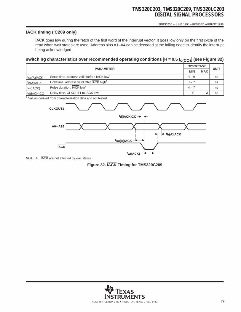
TMS320C203, TMS320C209, TMS320LC203DIGITAL SIGNAL PROCESSORS
SPRS025B – JUNE 1995 – REVISED AUGUST 1998
79POST OFFICE BOX 1443 • HOUSTON, TEXAS 77251–1443
IACK timing (’C209 only)
IACK goes low during the fetch of the first word of the interrupt vector. It goes low only on the first cycle of theread when wait states are used. Address pins A1–A4 can be decoded at the falling edge to identify the interruptbeing acknowledged.
switching characteristics over recommended operating conditions [H = 0.5 t c(CO)] (see Figure 32)
PARAMETER’320C209-57
UNITPARAMETERMIN MAX
UNIT
tsu(A)IACK Setup time, address valid before IACK low† H – 9 ns
th(A)IACK Hold time, address valid after IACK high† H – 7 ns
tw(IACK) Pulse duration, IACK low† H – 7 ns
td(IACK)CO Delay time, CLKOUT1 to IACK low – 1† 3 ns
† Values derived from characterization data and not tested
IACK
CLKOUT1
A0–A15
td(IACK)CO
th(A)IACK
tsu(A)IACK
tw(IACK)NOTE A: IACK are not affected by wait states.
Figure 32. IACK Timing for TMS320C209
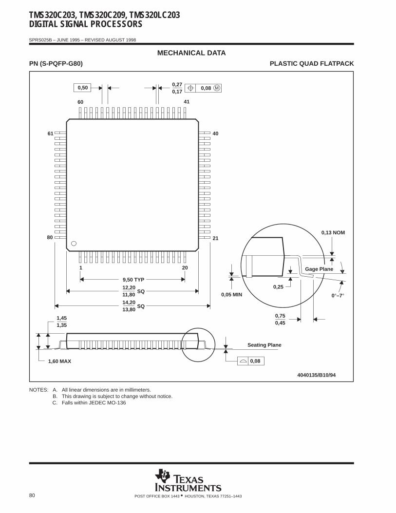
TMS320C203, TMS320C209, TMS320LC203DIGITAL SIGNAL PROCESSORS
SPRS025B – JUNE 1995 – REVISED AUGUST 1998
80 POST OFFICE BOX 1443 • HOUSTON, TEXAS 77251–1443
MECHANICAL DATAPN (S-PQFP-G80) PLASTIC QUAD FLATPACK
4040135/B10/94
0,170,27
0,13 NOM
40
21
0,25
0,450,75
0,05 MIN
Seating Plane
Gage Plane
4160
61
80
20
SQ
SQ
1
13,8014,20
12,20
9,50 TYP
11,80
1,451,35
1,60 MAX 0,08
0,50 M0,08
0°–7°
NOTES: A. All linear dimensions are in millimeters.B. This drawing is subject to change without notice.C. Falls within JEDEC MO-136
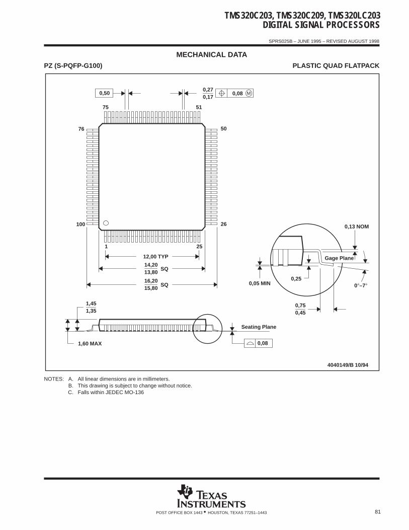
TMS320C203, TMS320C209, TMS320LC203DIGITAL SIGNAL PROCESSORS
SPRS025B – JUNE 1995 – REVISED AUGUST 1998
81POST OFFICE BOX 1443 • HOUSTON, TEXAS 77251–1443
MECHANICAL DATAPZ (S-PQFP-G100) PLASTIC QUAD FLATPACK
4040149/B 10/94
50
26 0,13 NOM
Gage Plane
0,25
0,450,75
0,05 MIN
0,27
51
25
75
1
12,00 TYP
0,17
76
100
SQ
SQ15,8016,20
13,80
1,351,45
1,60 MAX
14,20
0°–7°
Seating Plane
0,08
0,50 M0,08
NOTES: A. All linear dimensions are in millimeters.B. This drawing is subject to change without notice.C. Falls within JEDEC MO-136
IMPORTANT NOTICE
Texas Instruments and its subsidiaries (TI) reserve the right to make changes to their products or to discontinueany product or service without notice, and advise customers to obtain the latest version of relevant informationto verify, before placing orders, that information being relied on is current and complete. All products are soldsubject to the terms and conditions of sale supplied at the time of order acknowledgement, including thosepertaining to warranty, patent infringement, and limitation of liability.
TI warrants performance of its semiconductor products to the specifications applicable at the time of sale inaccordance with TI’s standard warranty. Testing and other quality control techniques are utilized to the extentTI deems necessary to support this warranty. Specific testing of all parameters of each device is not necessarilyperformed, except those mandated by government requirements.
CERTAIN APPLICATIONS USING SEMICONDUCTOR PRODUCTS MAY INVOLVE POTENTIAL RISKS OFDEATH, PERSONAL INJURY, OR SEVERE PROPERTY OR ENVIRONMENTAL DAMAGE (“CRITICALAPPLICATIONS”). TI SEMICONDUCTOR PRODUCTS ARE NOT DESIGNED, AUTHORIZED, ORWARRANTED TO BE SUITABLE FOR USE IN LIFE-SUPPORT DEVICES OR SYSTEMS OR OTHERCRITICAL APPLICATIONS. INCLUSION OF TI PRODUCTS IN SUCH APPLICATIONS IS UNDERSTOOD TOBE FULLY AT THE CUSTOMER’S RISK.
In order to minimize risks associated with the customer’s applications, adequate design and operatingsafeguards must be provided by the customer to minimize inherent or procedural hazards.
TI assumes no liability for applications assistance or customer product design. TI does not warrant or representthat any license, either express or implied, is granted under any patent right, copyright, mask work right, or otherintellectual property right of TI covering or relating to any combination, machine, or process in which suchsemiconductor products or services might be or are used. TI’s publication of information regarding any thirdparty’s products or services does not constitute TI’s approval, warranty or endorsement thereof.
Copyright 1998, Texas Instruments Incorporated
Related Documents