Chapter 2 C2xx DSP CPU AND INSTRUCTION SET

Welcome message from author
This document is posted to help you gain knowledge. Please leave a comment to let me know what you think about it! Share it to your friends and learn new things together.
Transcript
Chapter 2
C2xx DSP CPU AND
INSTRUCTION SET
Introduction to the C2xx DSP Core and Code
Generation
The heart of LF2407 DSP controller is the C2XX DSP core.
This core is a 16-bit fixed point processor, meaning that it works
with 16-bit binary number.
The LF2407 DSP consists of the C2xx DSP core plus many
peripherals such as Event Managers, ADC, etc., all integrated onto
one single chip.
The C2xx core has its own native instruction set of assembly
mnemonics or commands. Through the use of CCS and the
associated compiler, one has the freedom of writing code in both C
language and the native assembly language.
The Components of the C2xx DSP Core
The DSP core (like all microprocessors) consists of several subcomponents necessary to perform arithmetic operations on 16-bit binary numbers.
The subcomponent are
1. A 32-bit central arithmetic logic unit (CALU)
2. A 32-bit accumulator (used frequently in programs)
3. Input and output data-scaling shifters for the CALU
4. A (16-bit by 16-bit) multiplier
5. A product-scaling shifter
6. Eight auxiliary registers (AR0 – AR7) and an auxiliary register arithmetic unit (ARAU)
Each of the above components is either accessed directly bythe user code or is indirectly used during the execution of anassembly command.
Central Arithmetic Logic Unit (CALU)
The C2xx performs 2s-complement arithmetic using the 32-bit
CALU.
The CALU uses 16-bit words taken from data memory,
derived from an immediate instruction, or from the 32-bit
multiplier result.
In addition to arithmetic operations, the CALU can perform
Boolean operations.
The CALU is somewhat transparent to the user
i.e if an arithmetic command is used, the user only needs to
write the command and later read the output from the
appropriate register.
means, it is not accessed directly by the user.
Accumulator
The accumulator stores the output from the CALU and also
serves as another input to the CALU (many arithmetic
commands perform operations on numbers that are currently
stored in the accumulator; versus other memory locations).
The accumulator is 32 bits wide and is divided into two
sections, each consisting of 16 bits.
1. The high-order bits 31 to 16
2. The low-order bits 15 to 0
Assembly language instructions are provided for storing the
high- and low-order accumulator words to data memory.
Scaling Shifters
The C2xx has three 32-bit shifters that allow for scaling, bit
extraction, extended arithmetic, and overflow-prevention
operations.
The scaling shifters make possible commands that shift data
left or right.
There are following 3-shifters:
1. Input data-scaling shifter (input shifter)
2. Output data-scaling shifter (output shifter)
3. Product scaling shifter(product shifter)
The description of 3-shifter:
1. Input data-scaling shifter (input shifter)
This shifter left-shifts 16-bit input data by 0 to 16 bits to alignthe data to the 32-bit input of the CALU.
For example,
“ADD 300h, 5”, the input shifter is responsible for firstshifting the data in memory address “300h” to the left by fiveplaces before it is added to the contents of the accumulator.
2. Output data-scaling shifter(output shifter)
This shifter left-shifts data from the accumulator by 0 to 7 bits before the output is stored to data memory.
For example,
“SACL 300h, 4”, the output shifter is responsible for first shifting the contents of the accumulator to the left by four places before it is stored to the memory address “300h”.
3. Product-scaling shifter (product shifter)
The product register (PREG) receives the output of the multiplier. The product shifter shifts the output of the PREG before that output is sent to the input of the CALU.
Multiplier
The multiplier performs 16-bit, 2s-complement multiplication
and creates a 32-bit result.
In conjunction with the multiplier, the C2xx uses the 16-bit
temporary register (TREG) and the 32-bit product register
(PREG).
The TREG always needs to be loaded with one of the numbers
that are to be multiplied.
The output of the multiply is stored in the PREG.
Auxiliary Register Arithmetic Unit (ARAU)
and Auxiliary Registers
The ARAU generates data memory addresses when an
instruction uses indirect addressing to access data memory .
Eight auxiliary registers (AR0 through AR7) support the
ARAU, each of which can be loaded with a 16-bit value from
data memory or directly from an instruction.
Each auxiliary register value can also be stored in data
memory.
The auxiliary registers are mainly used as “pointers” to data
memory locations to more easily facilitate looping or repeating
algorithms.
The auxiliary register pointer (ARP) embedded in status
register ST0 references the auxiliary register.
Mapping External Devices to the C2xx Core
and the Peripheral Interface
the LF2407 contains many peripherals that need to be accessed
by the C2xx core, the C2xx needs a way to read and write to
the different peripherals.
Each peripheral is mapped to a corresponding block of data
memory addresses.
each corresponding block contains configuration registers,
input registers, output registers, and status registers.
Each peripheral is accessed by simply writing to the
appropriate registers in data memory, provided the peripheral
clock is enabled .
The peripherals are linked to the internal memory interface of
the CPU through the PBUS interface shown in Fig.
All on-chip peripherals are accessed through the Peripheral
Bus (PBUS).
All peripherals, excluding the WD timer counter, are clocked
by the CPU clock (which has a selectable frequency), and
must be enabled via the system configuration registers.
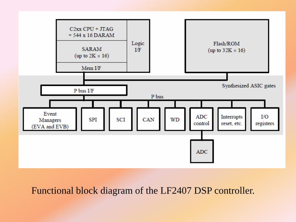
Functional block diagram of the LF2407 DSP controller.
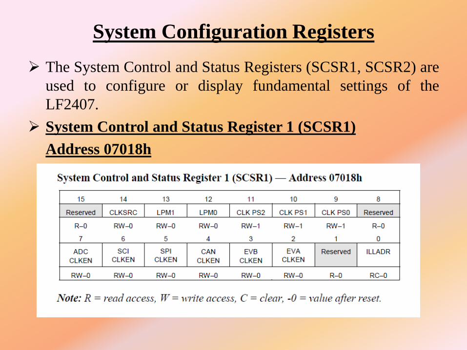
System Configuration Registers
The System Control and Status Registers (SCSR1, SCSR2) are
used to configure or display fundamental settings of the
LF2407.
System Control and Status Register 1 (SCSR1)
Address 07018h
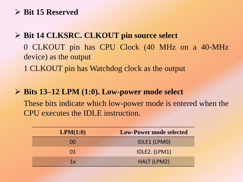
Bit 15 Reserved
Bit 14 CLKSRC. CLKOUT pin source select
0 CLKOUT pin has CPU Clock (40 MHz on a 40-MHz
device) as the output
1 CLKOUT pin has Watchdog clock as the output
Bits 13–12 LPM (1:0). Low-power mode select
These bits indicate which low-power mode is entered when the
CPU executes the IDLE instruction.
LPM(1:0) Low-Power mode selected
00 IDLE1 (LPM0)
01 IDLE2. (LPM1)
1x HALT (LPM2)
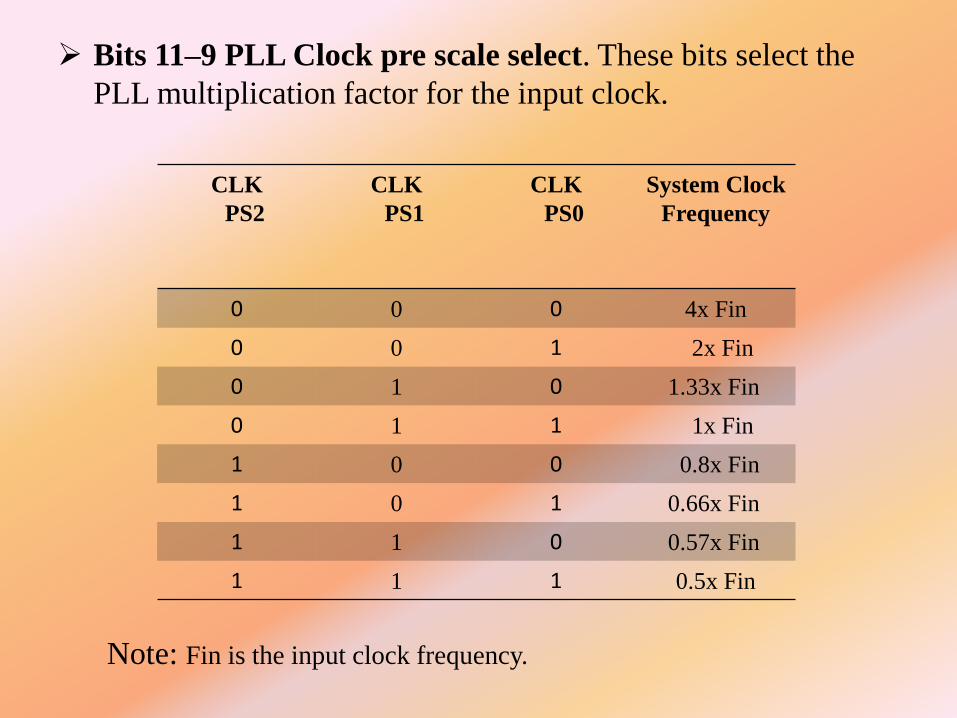
Bits 11–9 PLL Clock pre scale select. These bits select the
PLL multiplication factor for the input clock.
CLK
PS2
CLK
PS1
CLK
PS0
System Clock
Frequency
0 0 0 4x Fin
0 0 1 2x Fin
0 1 0 1.33x Fin
0 1 1 1x Fin
1 0 0 0.8x Fin
1 0 1 0.66x Fin
1 1 0 0.57x Fin
1 1 1 0.5x Fin
Note: Fin is the input clock frequency.
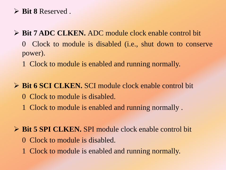
Bit 8 Reserved .
Bit 7 ADC CLKEN. ADC module clock enable control bit
0 Clock to module is disabled (i.e., shut down to conserve
power).
1 Clock to module is enabled and running normally.
Bit 6 SCI CLKEN. SCI module clock enable control bit
0 Clock to module is disabled.
1 Clock to module is enabled and running normally .
Bit 5 SPI CLKEN. SPI module clock enable control bit
0 Clock to module is disabled.
1 Clock to module is enabled and running normally.
Bit 4 CAN CLKEN. CAN module clock enable control bit
0 Clock to module is disabled
1 Clock to module is enabled and running normally
Bit 3 EVB CLKEN. EVB module clock enable control bit
0 Clock to module is disabled
1 Clock to module is enabled and running normally
Bit 2 EVA CLKEN. EVA module clock enable control bit
0 Clock to module is disabled
1 Clock to module is enabled and running normally
Bit 1 Reserved
Bit 0 ILLADR. Illegal Address detect bit
If an illegal address has occurred, this bit will be set. It is up to
software to clear this bit following an illegal address detect.
This bit is cleared by writing a 1 to it and should be cleared as
part of the initialization sequence. Note: An illegal address will
cause a Non-maskable Interrupt (NMI).
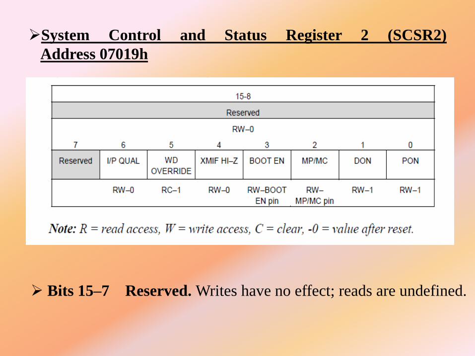
System Control and Status Register 2 (SCSR2)
Address 07019h
Bits 15–7 Reserved. Writes have no effect; reads are undefined.
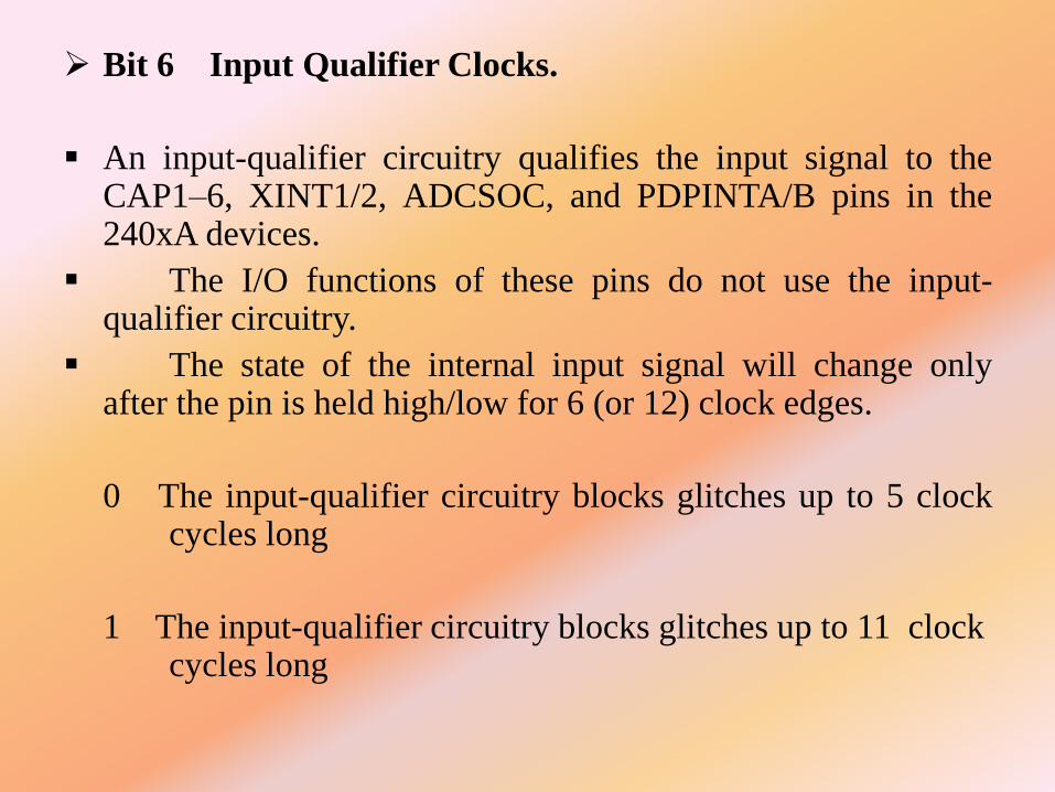
Bit 6 Input Qualifier Clocks.
An input-qualifier circuitry qualifies the input signal to theCAP1–6, XINT1/2, ADCSOC, and PDPINTA/B pins in the240xA devices.
The I/O functions of these pins do not use the input-qualifier circuitry.
The state of the internal input signal will change onlyafter the pin is held high/low for 6 (or 12) clock edges.
0 The input-qualifier circuitry blocks glitches up to 5 clockcycles long
1 The input-qualifier circuitry blocks glitches up to 11 clockcycles long
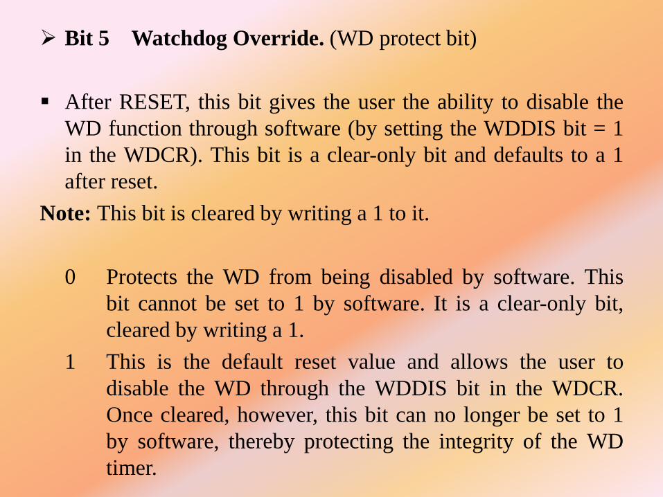
Bit 5 Watchdog Override. (WD protect bit)
After RESET, this bit gives the user the ability to disable the
WD function through software (by setting the WDDIS bit = 1
in the WDCR). This bit is a clear-only bit and defaults to a 1
after reset.
Note: This bit is cleared by writing a 1 to it.
0 Protects the WD from being disabled by software. This
bit cannot be set to 1 by software. It is a clear-only bit,
cleared by writing a 1.
1 This is the default reset value and allows the user to
disable the WD through the WDDIS bit in the WDCR.
Once cleared, however, this bit can no longer be set to 1
by software, thereby protecting the integrity of the WD
timer.
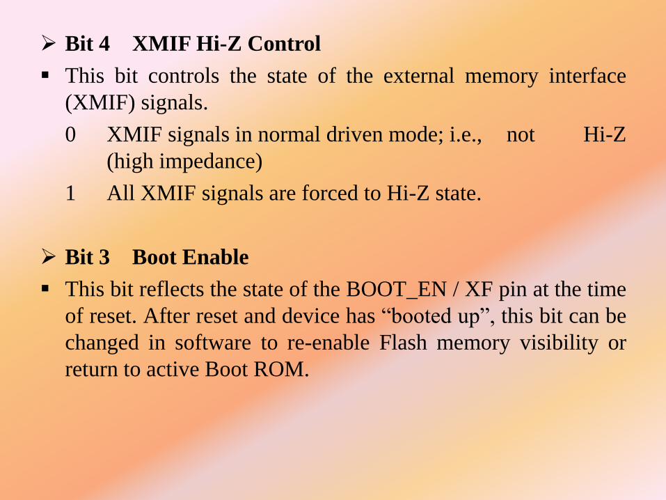
Bit 4 XMIF Hi-Z Control
This bit controls the state of the external memory interface
(XMIF) signals.
0 XMIF signals in normal driven mode; i.e., not Hi-Z
(high impedance)
1 All XMIF signals are forced to Hi-Z state.
Bit 3 Boot Enable
This bit reflects the state of the BOOT_EN / XF pin at the time
of reset. After reset and device has “booted up”, this bit can be
changed in software to re-enable Flash memory visibility or
return to active Boot ROM.
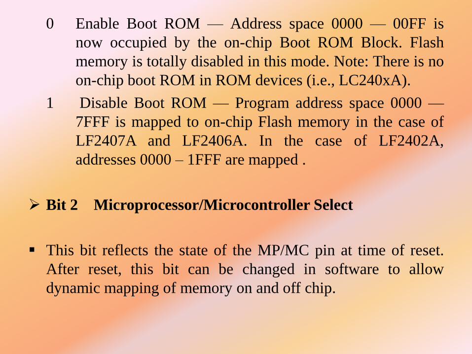
0 Enable Boot ROM — Address space 0000 — 00FF is
now occupied by the on-chip Boot ROM Block. Flash
memory is totally disabled in this mode. Note: There is no
on-chip boot ROM in ROM devices (i.e., LC240xA).
1 Disable Boot ROM — Program address space 0000 —
7FFF is mapped to on-chip Flash memory in the case of
LF2407A and LF2406A. In the case of LF2402A,
addresses 0000 – 1FFF are mapped .
Bit 2 Microprocessor/Microcontroller Select
This bit reflects the state of the MP/MC pin at time of reset.
After reset, this bit can be changed in software to allow
dynamic mapping of memory on and off chip.
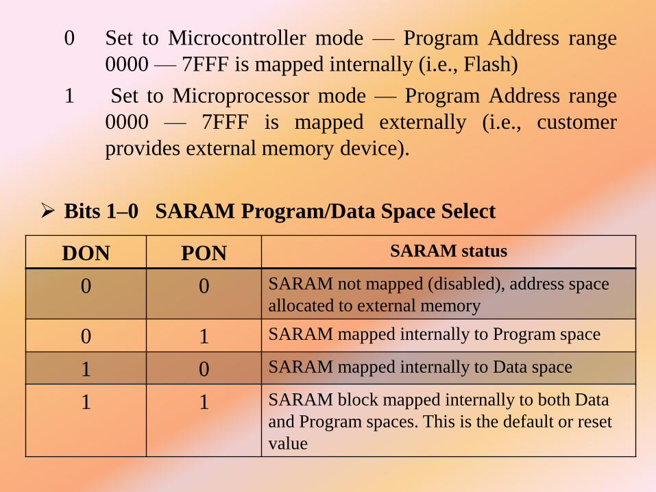
0 Set to Microcontroller mode — Program Address range
0000 — 7FFF is mapped internally (i.e., Flash)
1 Set to Microprocessor mode — Program Address range
0000 — 7FFF is mapped externally (i.e., customer
provides external memory device).
Bits 1–0 SARAM Program/Data Space Select
DON PON SARAM status
0 0 SARAM not mapped (disabled), address space
allocated to external memory
0 1 SARAM mapped internally to Program space
1 0 SARAM mapped internally to Data space
1 1 SARAM block mapped internally to both Data
and Program spaces. This is the default or reset
value
Memory
Memory is required to hold programs, perform operations, and
execute programming instructions.
There are three main blocks of memory which are present on
the LF2407 chip: B0, B1, and B2.
Additionally, there are two different memory “spaces”
(program, data) in which blocks are used.
Memory Blocks and Types
A block of memory on the LF2407 is simply a specified range
of memory addresses (each address consists of a 16-bit word
of memory).
The LF2407 has 544 16-bit words of on-chip Double AccessRandom Access Memory (DARAM) that are divided into threemain memory blocks named B0, B1, and B2.
In addition to the DARAM, there are also 2000 16-bit wordsof Single Access Random Access Memory (SARAM).
The main difference between DARAM and SARAM is thatDARAM memory can be accessed twice per clock cycle andSARAM can only be accessed once per cycle.
Thus, DARAM reads and writes twice as fast as SARAM.
In addition to the RAM present on the LF2407, there is alsonon-volatile Flash memory.
Unlike RAM, the Flash memory does not lose its contentswhen the LF2407 loses power.
Flash memory can only be written to by “flashing” thememory, which is a process that can only be done manually bya user.
Memory Space and Allocation
There are two ways of using the physical memory on board theLF2407: storing a program or storing data.
A program that is to be run must be stored in memory that ismapped to program space. Likewise, only memory that is indata space may be used to store data.
Program memory is written to when a program is loaded intothe LF2407. Data memory is normally written to during theexecution of a program, where the program might use the datamemory as temporary storage for calculation variables andresults.
Memory blocks B1 and B2 are configured as data memory.The B0 block is primarily intended to hold data, but can beconfigured to act as either program or data memory, dependingon the value of the CNF bit in Status Register ST1.
CNF = 0 maps B0 in data memory
CNF = 1 maps B0 in program memory.
The memory addresses associated with the SARAM can be
configured for both data memory and program memory, and
are also software configurable to either access external
memory or the internal SARAM.
When configured for internal, the SARAM can be used as
data or program memory. However, when configured as
external, these addresses are used for off-chip program
memory.
SARAM is useful if more memory is needed for data than the
B0, B1, and B2 blocks can provide.
The on-chip flash in the LF2407 is mapped to program
memory space when the external MP/MC-pin is pulled low.
When the MP/MC-pin is pulled high, the program memory is
mapped to external memory addresses .
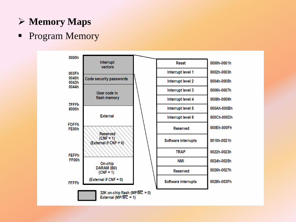
Memory Maps
Program Memory
Two factors determine the configuration of program memory:
CNF bit:
– The CNF bit determines if B0 memory is in on-chip program
space:
– CNF = 0. The 256 words are mapped as external memory.
– CNF = 1. The 256 words of DARAM B0 are configured for
program use. At reset, B0 is mapped to data space (CNF = 0).
MP/MC pin:
– The level on the MP/MC pin determines if program instructions
are read from on-chip Flash/ROM or external memory:
– MP/MC = 0. The device is configured in microcontroller mode.
The on-chip flash EEPROM is accessible. The device fetches the
reset vector from on-chip memory.
MP/MC = 1. The device is configured in microprocessor mode.
Program memory is mapped to external memory.
Data Memory
For the execution of a program, it is necessary to store
calculation results or look up tables in memory. The memory
allocated for this function is called data memory.
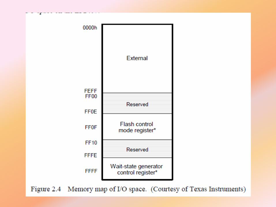
Input / Output (I/O) Space
I/O space is solely used for accessing external peripherals such
as the digital-to-analog converter (DAC) on the LF2407 EVM.
It is not to be confused with the I/O functionality of pins.
The assembly instruction “OUT” is used to write to an address
that is mapped to I/O space. Figure 2.4 depicts the basic
memory map of the I/O space on the LF2407.

Memory Addressing Modes
There are three basic memory addressing modes used by the
C2xx instruction set.
1. Immediate addressing mode (does not actually access
memory)
2. Direct addressing mode
3. Indirect addressing mode
Immediate addressing mode
In the immediate addressing mode, the instruction contains a
constant to be manipulated by the instruction.
The “#” sign indicates that the value is an immediate address
(just a constant).
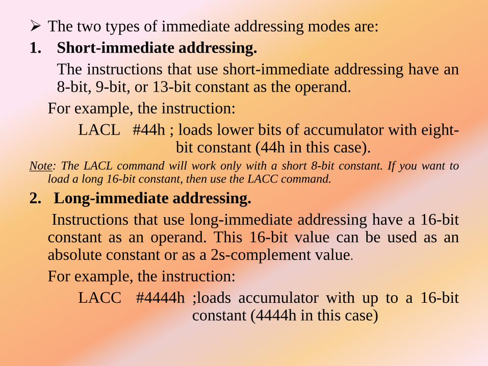
The two types of immediate addressing modes are:
1. Short-immediate addressing.
The instructions that use short-immediate addressing have an8-bit, 9-bit, or 13-bit constant as the operand.
For example, the instruction:
LACL #44h ; loads lower bits of accumulator with eight-bit constant (44h in this case).
Note: The LACL command will work only with a short 8-bit constant. If you want toload a long 16-bit constant, then use the LACC command.
2. Long-immediate addressing.
Instructions that use long-immediate addressing have a 16-bitconstant as an operand. This 16-bit value can be used as anabsolute constant or as a 2s-complement value.
For example, the instruction:
LACC #4444h ;loads accumulator with up to a 16-bitconstant (4444h in this case)
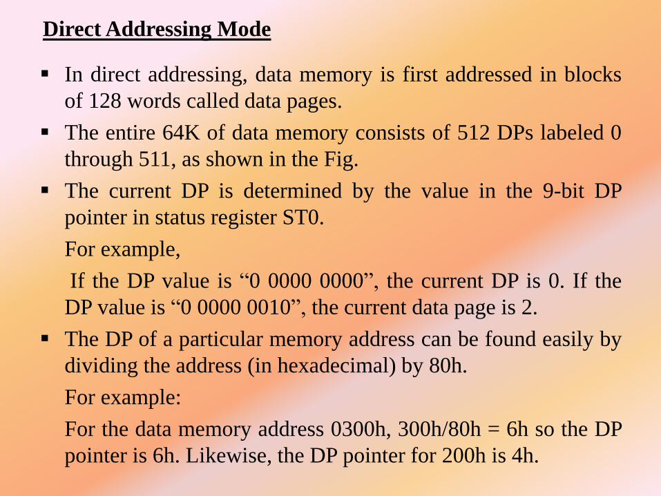
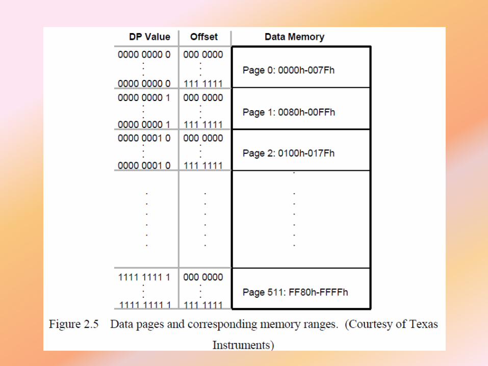
Direct Addressing Mode
In direct addressing, data memory is first addressed in blocks
of 128 words called data pages.
The entire 64K of data memory consists of 512 DPs labeled 0
through 511, as shown in the Fig.
The current DP is determined by the value in the 9-bit DP
pointer in status register ST0.
For example,
If the DP value is “0 0000 0000”, the current DP is 0. If the
DP value is “0 0000 0010”, the current data page is 2.
The DP of a particular memory address can be found easily by
dividing the address (in hexadecimal) by 80h.
For example:
For the data memory address 0300h, 300h/80h = 6h so the DP
pointer is 6h. Likewise, the DP pointer for 200h is 4h.
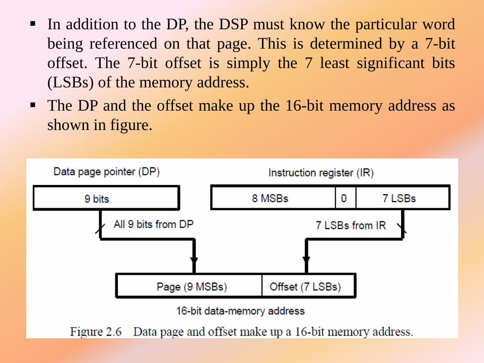
In addition to the DP, the DSP must know the particular word
being referenced on that page. This is determined by a 7-bit
offset. The 7-bit offset is simply the 7 least significant bits
(LSBs) of the memory address.
The DP and the offset make up the 16-bit memory address as
shown in figure.
When you use direct addressing, the processor uses the 9 DP
bits and the 7 LSBs of the instruction to obtain the true
memory address.
The following steps should be followed when using direct
addressing:
1. Set the DP. Load the appropriate value (from 0 to 511 in
decimal or 0-1FF in hex) into the DP. The easiest way to do
this is with the LDP instruction.
The LDP instruction loads the DP directly to the ST0 register
without affecting any other bits of the ST0.
LDP #0E1h ; sets the data page pointer to E1h OR
LDP #225 ; sets the data page pointer to 225 decimal
;which is E1 in hexadecimal
2. Specify the offset. For example, if you want the ADD
instruction to use the value at the second address of the current
data page, you would write: ADD 1h
If the data page points to 300h, then the above instruction will
add the contents of 301h to the accumulator.
Indirect Addressing Mode
Indirect addressing is a powerful way of addressing data
memory.
Indirect addressing mode is not dependent on the current data
page as is direct addressing. Instead, when using indirect
addressing you load the memory space that you would like to
access into one of the auxiliary registers (ARx).
The current auxiliary register acts as a pointer that points to a
specific memory address.
The register pointed to by the ARP is referred to as the current
auxiliary register or current AR.
To select a specific auxiliary register, load the 3-bit auxiliary
register pointer (ARP) with a value from 0 to 7. The ARP can
be loaded with the MAR instruction or by the LARP
instruction.
An ARP value can also be loaded by using the ARx operand
after any instruction that supports indirect addressing as seen
below.
Example of using MAR:
ADD * , AR1 ;Adds using current *,then makes AR1
;the new current AR for future uses
Example of using LARP:
LARP #2 ;this will make AR2 the current AR
The C2xx provides four types of indirect addressing options:
1. No increment or decrement.
The instruction uses the content of the current auxiliary register as thedata memory address but neither increments nor decrements thecontent of the current auxiliary register.
2. Increment or decrement by 1.
The instruction uses the content of the current auxiliary register as thedata memory address and then increments or decrements the contentof the current auxiliary register by one.
3. Increment or decrement by an index amount.
The value in AR0 is the index amount. The instruction uses the contentof the current auxiliary register as the data memory address and thenincrements or decrements the content of the current auxiliary registerby the index amount.
4. Increment or decrement by an index amount using reverse carry.The value in AR0 is the index amount. After the instruction uses thecontent of the current auxiliary register as the data memory address,that content is incremented or decremented by the index amount. Theaddition and subtraction process is accomplished with the carrypropagation reversed and is useful in fast Fourier transformsalgorithms.
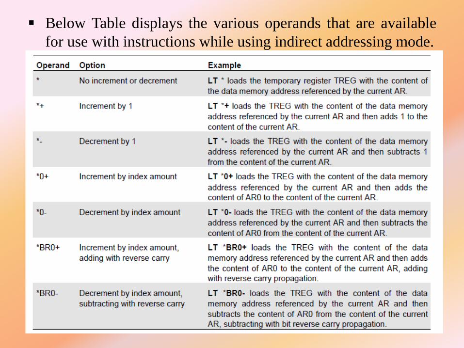
Below Table displays the various operands that are available
for use with instructions while using indirect addressing mode.
Related Documents