MGM’s Jawaharlal Nehru Engineering College Aurangabad Affiliated to Dr.B.A.Technological University , Lonere Maharashtra ISO 9001:2015,140001:2015 Certified, AICTE Approved Department of Computer Science & Engineering LAB MANUAL Programme (UG/PG) : UG Year : Second Year Semester : III Course Code : BTCOL310 Course Title : Digital Electronics & Microprocessor Lab Prepared By Ms. V S Hanmante Assistant Professor Department of Computer Science & Engineering

Welcome message from author
This document is posted to help you gain knowledge. Please leave a comment to let me know what you think about it! Share it to your friends and learn new things together.
Transcript

MGM’s
Jawaharlal Nehru Engineering College Aurangabad Affiliated to Dr.B.A.Technological University , Lonere Maharashtra
ISO 9001:2015,140001:2015 Certified, AICTE Approved
Department of Computer Science & Engineering
LAB MANUAL
Programme (UG/PG) : UG
Year : Second Year
Semester : III
Course Code : BTCOL310
Course Title : Digital Electronics & Microprocessor Lab
Prepared By
Ms. V S Hanmante
Assistant Professor
Department of Computer Science & Engineering

FOREWORD
It is my great pleasure to present this laboratory manual for Second
year engineering students for the subject of Digital Electronics &
Microprocessor.
As a student, many of you may be wondering with some of the
questions in your mind regarding the subject and exactly what has
been tried is to answer through this manual.
As you may be aware that MGM has already been awarded with ISO
9001:2015, 140001:2015 certification and it is our endure to
technically equip our students taking the advantage of the procedural
aspects of ISO Certification.
Faculty members are also advised that covering these aspects in initial
stage itself, will greatly relived them in future as much of the load will
be taken care by the enthusiasm energies of the students once they are
conceptually clear.
Dr. H. H. Shinde
Principal

LABORATORY MANUAL CONTENTS
This manual is intended for the Second year students of Computer
Science and Engineering in the subject of Digital Electronics &
Microprocessor. This manual typically contains practical/Lab
Sessions related Digital Electronics & Microprocessor covering
various aspects related the subject to enhanced understanding.
Students are advised to thoroughly go through this manual rather than
only topics mentioned in the syllabus as practical aspects are the key
to understanding and conceptual visualization of theoretical aspects
covered in the books.
Good Luck for your Enjoyable Laboratory Sessions
Ms. V S Hanmante Dr. Vijaya Musande
Subject Teacher HOD
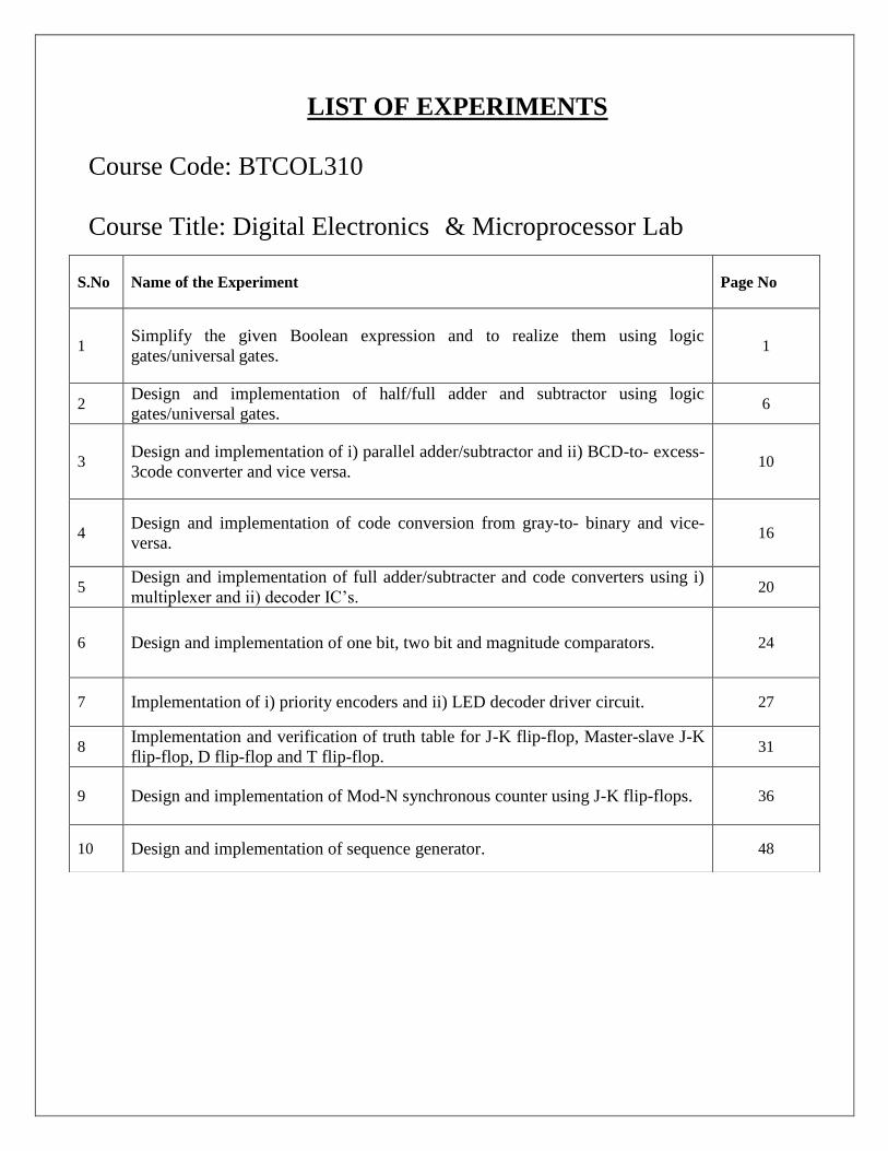
LIST OF EXPERIMENTS
Course Code: BTCOL310
Course Title: Digital Electronics & Microprocessor Lab
S.No Name of the Experiment Page No
1 Simplify the given Boolean expression and to realize them using logic
gates/universal gates. 1
2 Design and implementation of half/full adder and subtractor using logic
gates/universal gates. 6
3 Design and implementation of i) parallel adder/subtractor and ii) BCD-to- excess-
3code converter and vice versa. 10
4 Design and implementation of code conversion from gray-to- binary and vice-
versa. 16
5 Design and implementation of full adder/subtracter and code converters using i)
multiplexer and ii) decoder IC’s. 20
6 Design and implementation of one bit, two bit and magnitude comparators. 24
7 Implementation of i) priority encoders and ii) LED decoder driver circuit. 27
8 Implementation and verification of truth table for J-K flip-flop, Master-slave J-K
flip-flop, D flip-flop and T flip-flop. 31
9 Design and implementation of Mod-N synchronous counter using J-K flip-flops. 36
10 Design and implementation of sequence generator. 48

DOs and DON’Ts in Laboratory:
1. Make entry in the Log Book as soon as you enter the Laboratory.
2. All the students should sit according to their roll numbers starting from
their left to right.
3. All the students are supposed to enter the terminal number in the log book.
4. Do not change the terminal on which you are working.
5. All the students are expected to get at least the algorithm of the
program/concept to be implemented.
6. Strictly observe the instructions given by the teacher/Lab Instructor.
7. Do not disturb machine Hardware / Software Setup.
Instruction for Laboratory Teachers:
1. Submission related to whatever lab work has been completed should be
done during the next lab session along with signing the index.
2. The promptness of submission should be encouraged by way of marking
and evaluation patterns that will benefit the sincere students.
3. Continuous assessment in the prescribed format must be followed.

LABORATORY OUTCOMES
The practical/exercises in this section are psychomotor domain
Learning Outcomes (i.e. subcomponents of the COs), to be developed
and assessed to lead to the attainment of the competency.
CO-1: Simplify, design and implement Boolean expression/half and
full adders using basic/universal gates.
CO-2: Design and implement the various combinational circuits using
MSI components.
CO-3: Implement and verify the truth tables of various flip-flops.
CO-4: Design and implement the counters.
CO-5 : Design and implement the sequence generator.
1
EXPERIMENT: 1
Simplify the given Boolean expression and to realize them using logic
gates/universal gates.
AIM: To simplify the given expression and to realize it using basic gates and universal gates.
LEARNING OBJECTIVE:
i) Simplify the Boolean expression and build the logic circuit.
ii) For a given truth table derive the Boolean expressions and build the logic circuit to
realize it.
COMPONENTS REQUIRED:
IC 7400, IC 7408, IC 7432, IC 7406, IC 7402, Patch cords and IC Trainer Kit.
THEORY:
A Karnaugh map (K-map) is a graphical method used to minimize Boolean expressions
without having to use Boolean algebra theorems and equation manipulations. A K-map can be
thought of as a special version of a truth table. Using a K-map, expressions with two to four
variables are easily minimized.
Canonical Forms (Normal Forms): Any Boolean function can be written in disjunctive
normal form (sum of min-terms) or conjunctive normal form (product of max-terms). A Boolean
function can be represented by a Karnaugh map in which each cell corresponds to a minterm.
The cells are arranged in such a way that any two immediately adjacent cells correspond to two
minterms of distance 1. There is more than one way to construct a map with this property.
Karnaugh Maps
For a function of two variables, say, f(x, y),
For a function of three variables, say, f(x, y, z)
2
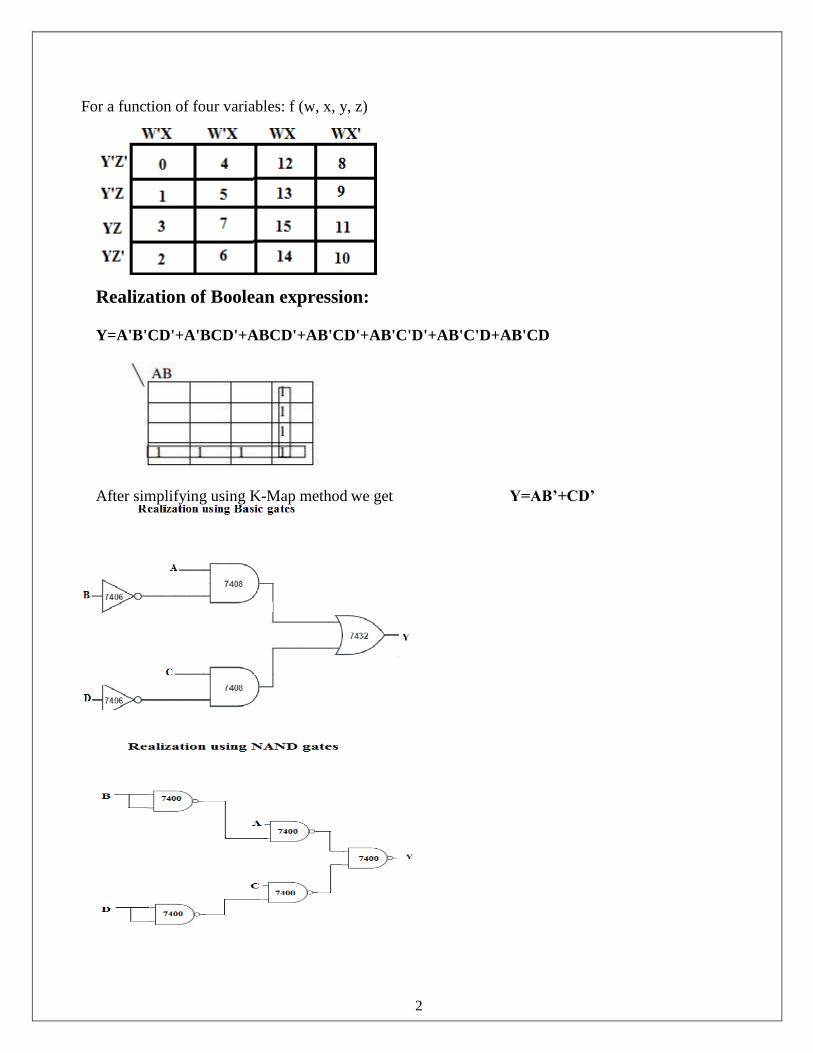
For a function of four variables: f (w, x, y, z)
Realization of Boolean expression:
Y=A'B'CD'+A'BCD'+ABCD'+AB'CD'+AB'C'D'+AB'C'D+AB'CD
After simplifying using K-Map method we get Y=AB’+CD’
3
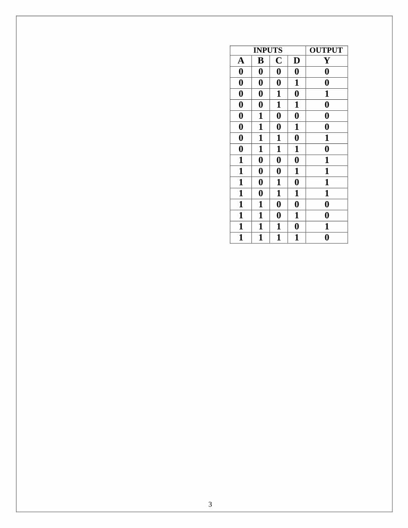
INPUTS OUTPUT
A B C D Y
0 0 0 0 0
0 0 0 1 0
0 0 1 0 1
0 0 1 1 0
0 1 0 0 0
0 1 0 1 0
0 1 1 0 1
0 1 1 1 0
1 0 0 0 1
1 0 0 1 1
1 0 1 0 1
1 0 1 1 1
1 1 0 0 0
1 1 0 1 0
1 1 1 0 1
1 1 1 1 0
4
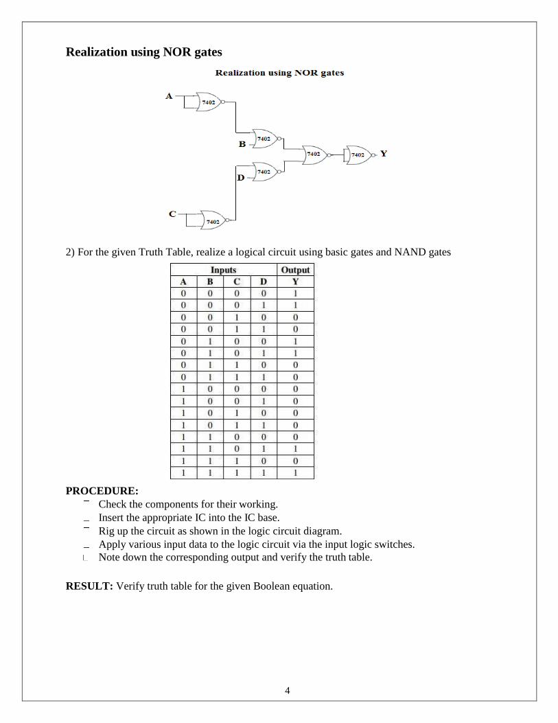
Realization using NOR gates
2) For the given Truth Table, realize a logical circuit using basic gates and NAND gates
PROCEDURE:
Check the components for their working.
Insert the appropriate IC into the IC base.
Rig up the circuit as shown in the logic circuit diagram.
Apply various input data to the logic circuit via the input logic switches.
Note down the corresponding output and verify the truth table.
RESULT: Verify truth table for the given Boolean equation.

5
EXPERIMENT: 2
Design and implementation of half/full adder and subtractor using logic
gates/universal gates
AIM: To design and verify – i) Half adder and Full adder
ii) Half subtractor and Full subtractor using basic and NAND gates.
LEARNING OBJECTIVE:
To design, realize and verify the adder and subtractor circuits using basic gates and
universal gates.
To design, realize and verify full adder using two half adders.
To design, realize and verify a full subtractor using two half subtractors.
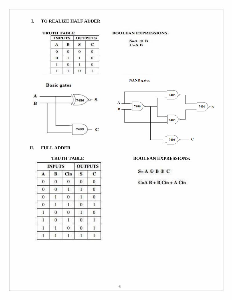
COMPONENTS REQUIRED: IC 7400, IC 7408, IC 7486, and IC 7432, Patch cords and IC
Trainer Kit.
THEORY:
Half-Adder: A combinational logic circuit that performs the addition of two data bits, A and B,
is called a half-adder. Addition will result in two output bits; one of which is the sum bit, S, and
the other is the carry bit, C. The Boolean functions describing the half-adder are:
S =A Ex-OR B C = A B
Full-Adder: The half-adder does not take the carry bit from its previous stage into account. This
carry bit from its previous stage is called carry-in bit. A combinational logic circuit that adds
two data bits, A and B, and a carry-in bit, Cin, is called a full-adder. The Boolean functions
describing the full-adder are:
S = (x Ex-OR y) Ex-OR Cin C = xy + Cin (x Ex-OR y)
Half Subtractor: Subtracting a single-bit binary value B from another A (i.e. A -B) produces a
difference bit D and a borrow out bit B-out. This operation is called half subtraction and the
circuit to realize it is called a half subtractor. The Boolean functions describing the half
Subtractor are:
D =A Ex-OR B Br = A’ B Full Subtractor: Subtracting two single-bit binary values, B, Cin from a single-bit value A
produces a difference bit D and a borrow out Br bit. This is called full subtraction. The Boolean
functions describing the full-subtractor are:
D = (x Ex-OR y) Ex-OR Cin Br= A’B + A’ (Cin) + B (Cin)
6
I. TO REALIZE HALF ADDER
II. FULL ADDER
TRUTH TABLE BOOLEAN EXPRESSIONS:

7
INPUTS OUTPUT
A B D Br
0 0 0 0
0 1 1 1
1 0 1 0
1 1 0 0
BASIC GATES
i) NAND GATES
III. HALF SUBTRACTOR
TRUTH TABLE BOOLEAN EXPRESSIONS:

8
IV. FULL SUBTRACTOR
TRUTH TABLE BOOLEAN EXPRESSIONS:
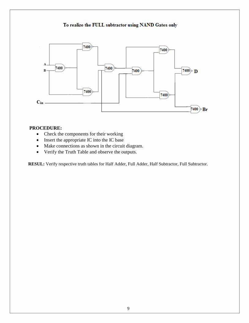
9
PROCEDURE:
Check the components for their working
Insert the appropriate IC into the IC base
Make connections as shown in the circuit diagram.
Verify the Truth Table and observe the outputs.
RESUL: Verify respective truth tables for Half Adder, Full Adder, Half Subtractor, Full Subtractor.

10
Experiment: 3

11
PARALLEL ADDER / SUBTRACTOR AND CODE CONVERTORS
Aim: To design and set up the following:
1. 4 bit binary adder and Subtractor.
2. Code conversion BCD to Excess-3 and vice versa.
Learning objective:
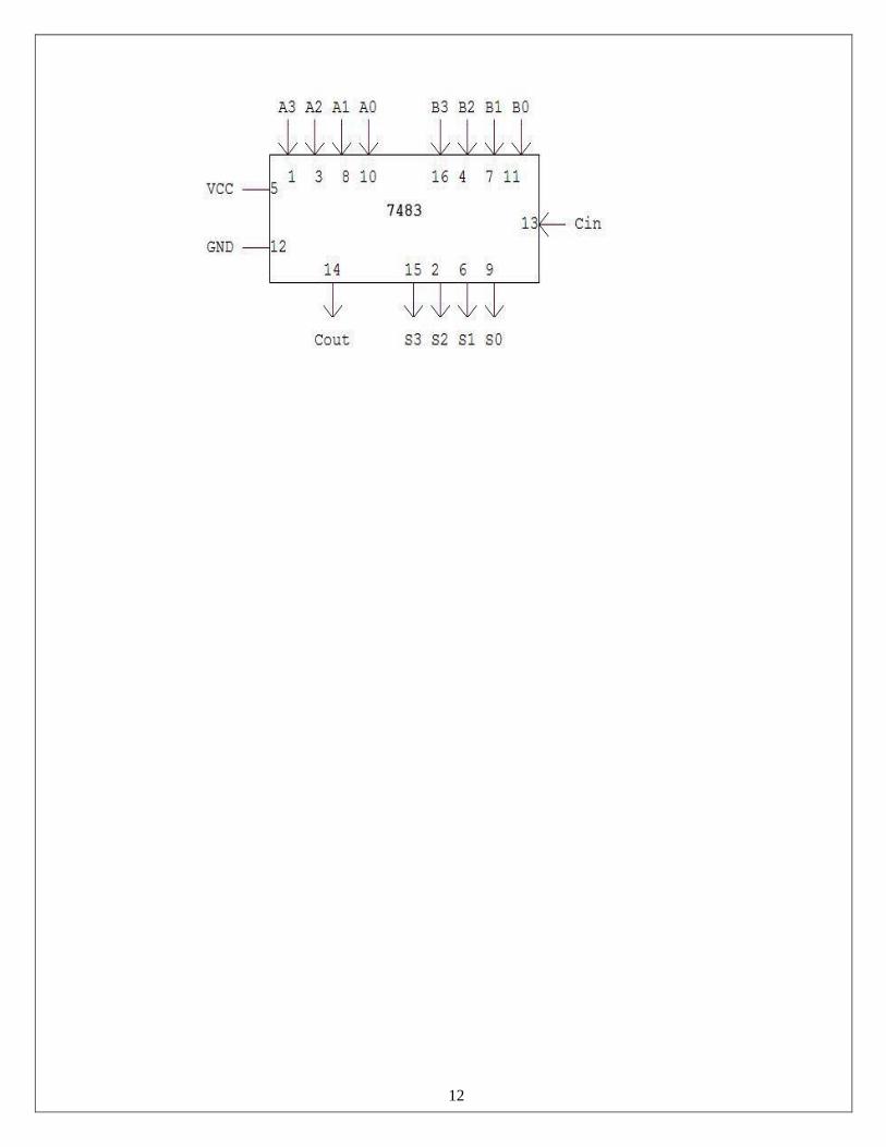
To learn about IC 7483 and its internal structure.
To realize a Subtractor using adder IC 7483.
Components required: IC 7483, IC 7486 trainer kit, patch cords.
Theory:
The Full adder can add single-digit binary numbers and carries. The largest sum that can be
obtained using a full adder is 112. Parallel adders can add multiple-digit numbers. If full adders
are placed in parallel, we can add two- or four-digit numbers or any other size desired. Figure
below uses standard symbols to show a parallel adder capable of adding two; two-digit binary
numbers. The addend would be on A inputs, and the augend on the B inputs. For this explanation
we will assume there is no input to C0 (carry from a previous circuit)
To add 102 (addend) and 012 (augend), the addend inputs will be 1 on A2 and 0 on A1. The
augend inputs will be 0 on B2 and 1 on B1. Working from right to left, as we do in normal
addition, let’s calculate the outputs of each full adder. With A1 at 0 and B1 at 1, the output of
adder1 will be a sum (S1) of 1 with no carry (C1). Since A2 is 1 and B2 is 0, we have a sum (S2)
of 1 with no carry (C2) from adder1. To determine the sum, read the outputs (C2, S2, and S1)
from left to right. In this case, C2 = 0, S2 = 1, and S1 = 1. The sum, then, of 102 and 012
is 0112.
Circuit implementation:
4 Bit Binary Adder:
An Example: 7+2=11 (1001)
7 is realized at A3 A2 A1 A0 = 0111
2 is realized at B3 B2 B1 B0 = 0010
Sum = 1001
12

13
Truth table:
Inputs A Inputs B Sum
A4 A3 A2 A1 B4 B3 B2 B1 S4 S3 S2 S1
4 Bit Binary Subtractor:
Subtraction is carried out by adding 2’s complement of the subtrahend. Example: 8 – 3 = 5
(0101)
8 is realized at A3 A2 A1 A0 = 1000
3 is realized at B3 B2 B1 B0 through X-OR gates = 0011
Output of X-OR gate is 1’s complement of 3 = 1100
2’s Complement can be obtained by adding Cin =1
Therefore
Cin = 1
A3 A2 A1 A0 = 1 0 0 0
B3 B2 B1 B0 = 1 1 0 0
S3 S2 S1 S0 = 0 1 0 1
Cout = 1 (Ignored)
Truth table:
Inputs A Inputs B Difference
A4 A3 A2 A1 B4 B3 B2 B1 S4 S3 S2 S1
14
Procedure:
Check the components for their working.
Insert the appropriate IC into the IC base.
Rig up the circuit as shown in the logic circuit diagram.
Apply various input data to the logic circuit via the input logic switches.
Note down the corresponding output and verify the truth table.
Result:
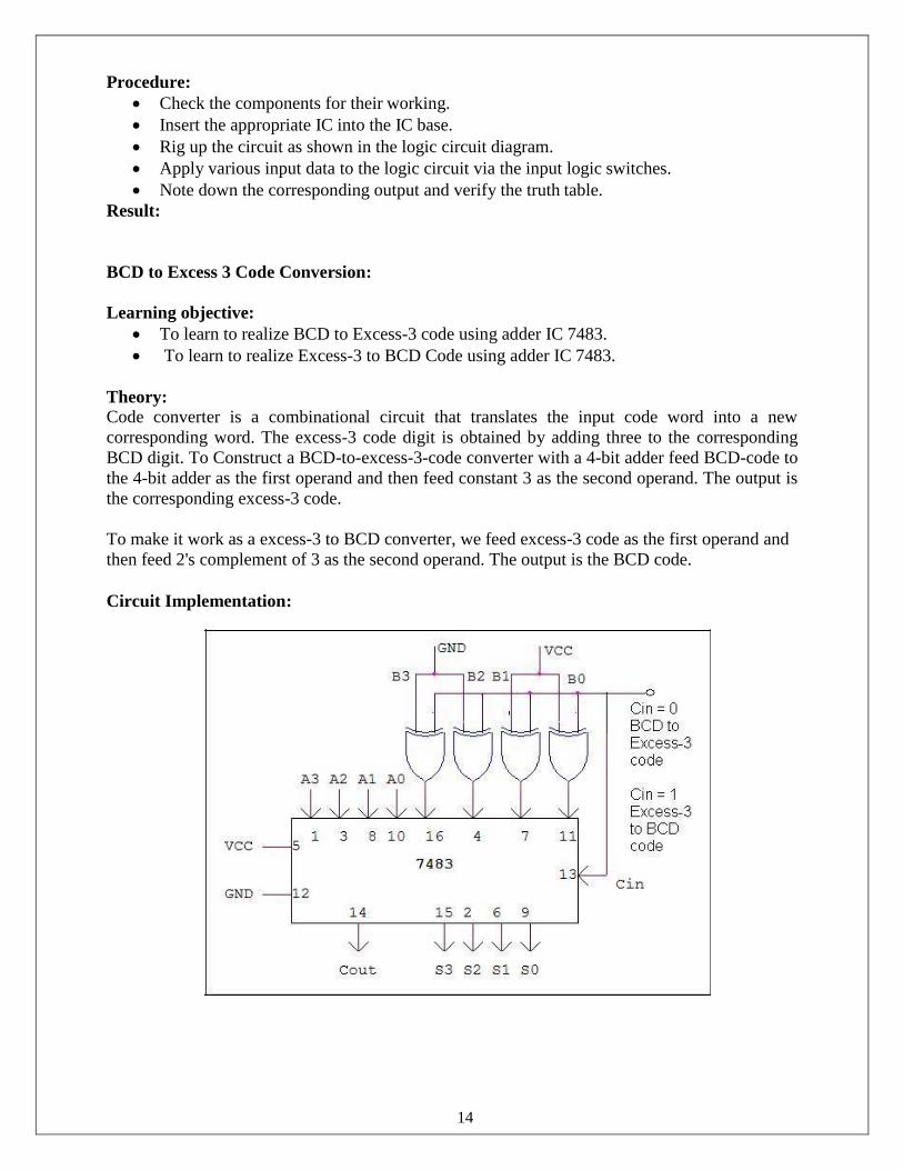
BCD to Excess 3 Code Conversion:
Learning objective:
To learn to realize BCD to Excess-3 code using adder IC 7483.
To learn to realize Excess-3 to BCD Code using adder IC 7483.
Theory:
Code converter is a combinational circuit that translates the input code word into a new
corresponding word. The excess-3 code digit is obtained by adding three to the corresponding
BCD digit. To Construct a BCD-to-excess-3-code converter with a 4-bit adder feed BCD-code to
the 4-bit adder as the first operand and then feed constant 3 as the second operand. The output is
the corresponding excess-3 code.
To make it work as a excess-3 to BCD converter, we feed excess-3 code as the first operand and
then feed 2's complement of 3 as the second operand. The output is the BCD code.
Circuit Implementation:
15
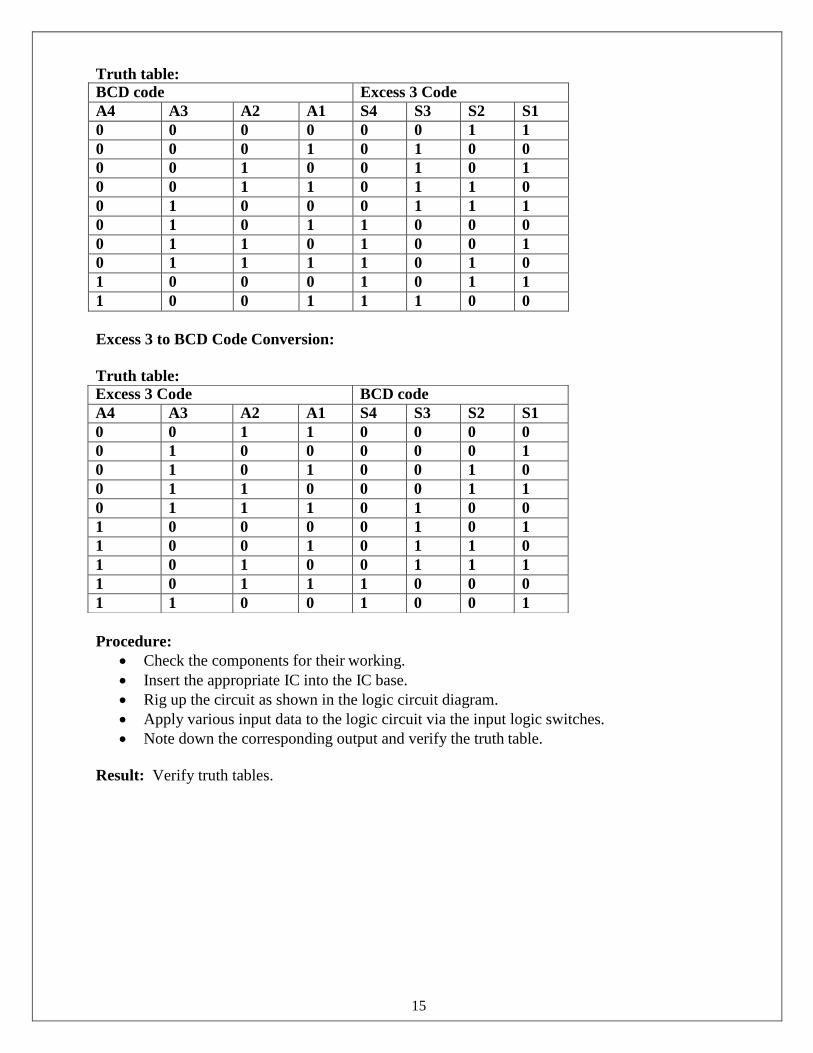
Truth table:
BCD code Excess 3 Code
A4 A3 A2 A1 S4 S3 S2 S1
0 0 0 0 0 0 1 1
0 0 0 1 0 1 0 0
0 0 1 0 0 1 0 1
0 0 1 1 0 1 1 0
0 1 0 0 0 1 1 1
0 1 0 1 1 0 0 0
0 1 1 0 1 0 0 1
0 1 1 1 1 0 1 0
1 0 0 0 1 0 1 1
1 0 0 1 1 1 0 0
Excess 3 to BCD Code Conversion:
Truth table:
Procedure:
Check the components for their working.
Insert the appropriate IC into the IC base.
Rig up the circuit as shown in the logic circuit diagram.
Apply various input data to the logic circuit via the input logic switches.
Note down the corresponding output and verify the truth table.
Result: Verify truth tables.
Excess 3 Code BCD code
A4 A3 A2 A1 S4 S3 S2 S1
0 0 1 1 0 0 0 0
0 1 0 0 0 0 0 1
0 1 0 1 0 0 1 0
0 1 1 0 0 0 1 1
0 1 1 1 0 1 0 0
1 0 0 0 0 1 0 1
1 0 0 1 0 1 1 0
1 0 1 0 0 1 1 1
1 0 1 1 1 0 0 0
1 1 0 0 1 0 0 1
16
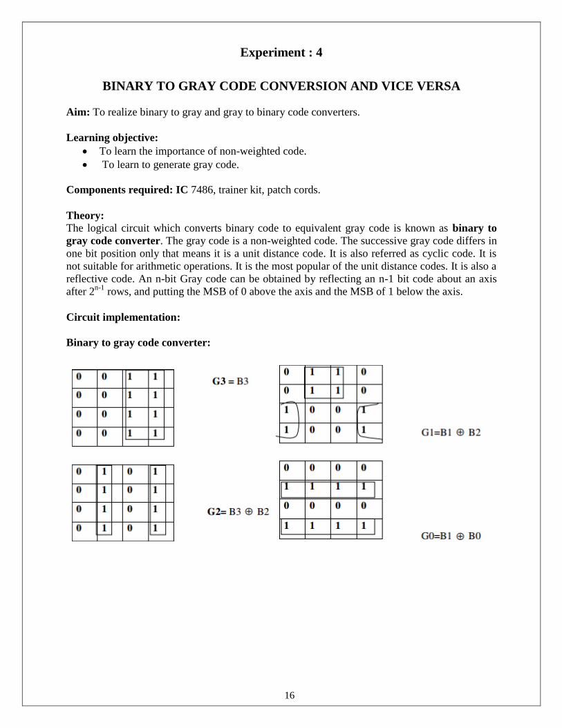
Experiment : 4
BINARY TO GRAY CODE CONVERSION AND VICE VERSA
Aim: To realize binary to gray and gray to binary code converters.
Learning objective:
To learn the importance of non-weighted code.
To learn to generate gray code.
Components required: IC 7486, trainer kit, patch cords.
Theory:
The logical circuit which converts binary code to equivalent gray code is known as binary to
gray code converter. The gray code is a non-weighted code. The successive gray code differs in
one bit position only that means it is a unit distance code. It is also referred as cyclic code. It is
not suitable for arithmetic operations. It is the most popular of the unit distance codes. It is also a
reflective code. An n-bit Gray code can be obtained by reflecting an n-1 bit code about an axis
after 2n-1
rows, and putting the MSB of 0 above the axis and the MSB of 1 below the axis.
Circuit implementation:
Binary to gray code converter:
17
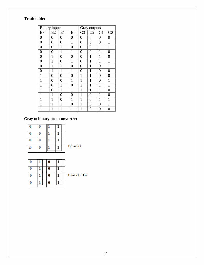
Truth table:
Binary inputs Gray outputs
B3 B2 B1 B0 G3 G2 G1 G0
0 0 0 0 0 0 0 0
0 0 0 1 0 0 0 1
0 0 1 0 0 0 1 1
0 0 1 1 0 0 1 0
0 1 0 0 0 1 1 0
0 1 0 1 0 1 1 1
0 1 1 0 0 1 0 1
0 1 1 1 0 1 0 0
1 0 0 0 1 1 0 0
1 0 0 1 1 1 0 1
1 0 1 0 1 1 1 1
1 0 1 1 1 1 1 0
1 1 0 0 1 0 1 0
1 1 0 1 1 0 1 1
1 1 1 0 1 0 0 1
1 1 1 1 1 0 0 0
Gray to binary code converter:

18
Truth table:
Gray inputs Binary outputs
G3 G2 G1 G0 B3 B2 B1 B0
0 0 0 0 0 0 0 0
0 0 0 1 0 0 0 1
0 0 1 0 0 0 1 1
0 0 1 1 0 0 1 0
0 1 0 0 0 1 1 1
0 1 0 1 0 1 1 0
0 1 1 0 0 1 0 0
0 1 1 1 0 1 0 1
1 0 0 0 1 1 1 1
1 0 0 1 1 1 1 0
1 0 1 0 1 1 0 0
1 0 1 1 1 1 0 1
1 1 0 0 1 0 0 0
1 1 0 1 1 0 0 1
1 1 1 0 1 0 1 1
1 1 1 1 1 0 1 0

19
Procedure:
Check the components for their working.
Insert the appropriate IC into the IC base.
Rig up the circuit as shown in the logic circuit diagram.
Apply various input data to the logic circuit via the input logic switches.
Note down the corresponding output and verify the truth table.
Result: Verify truth tables.

20
EXPERIMENT: 5
MULTIPLEXER AND DEMULTIPLEXER
AIM: To design and set up the following circuit 1) To verify the various functions of IC 74153(MUX) and IC 74139(DEMUX).
2) Half/Full Adder and Half/Full Subtractor using IC 74153 and IC 74139.
LEARNING OBJECTIVE:
To learn about various applications of multiplexer and de- multiplexer
To learn and understand the working of IC 74153 and IC 74139, and realize Half/Full Adder /Subtractor function using Multiplexer/De-multiplexer.
THEORY:
Multiplexers are very useful components in digital systems. They transfer a large number of information units over a smaller number of channels, (usually one channel) under the control of selection signals. Multiplexer means many to one. A multiplexer is a circuit with many inputs but only one output. By using control signals (select lines) we can select any input to the output. Multiplexer is also called as data selector because the output bit depends on the input data bit that is selected. The general multiplexer circuit has 2
n input signals, n control/select signals and 1 output signal.
De-multiplexers perform the opposite function of multiplexers. They transfer a small number of information units (usually one unit) over a larger number of channels under the control of selection signals. The general de-multiplexer circuit has 1 input signal, n control/select signals and 2
n output signals. De-multiplexer circuit can also be realized
using a decoder circuit with enable.
COMPONENTS REQUIRED:
IC 7400, IC 7410, IC 7420, IC 7404, IC 74153, IC 74139, Patch Cords & IC Trainer Kit.
i) 4:1 MULTIPLEXER
4:1
Inputs MUX Y
E’
Select inputs
Output Y= E’S1’S0’I0 + E’S1’S0I1 + E’S1S0’I2 + E’S1S0I3
21
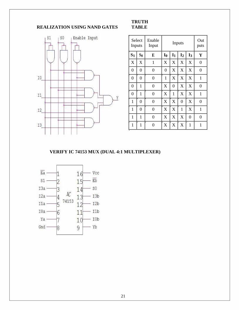
REALIZATION USING NAND GATES
TRUTH
TABLE
Select Inputs
Enable Input
Inputs Out puts
S1 S0 E I0 I1 I2 I3 Y
X X 1 X X X X 0
0 0 0 0 X X X 0
0 0 0 1 X X X 1
0 1 0 X 0 X X 0
0 1 0 X 1 X X 1
1 0 0 X X 0 X 0
1 0 0 X X 1 X 1
1 1 0 X X X 0 0
1 1 0 X X X 1 1
VERIFY IC 74153 MUX (DUAL 4:1 MULTIPLEXER)
20
Inputs Outputs
Ea S1 S0 Y3 Y2 Y1 Y0
1 X X 1 1 1 1
0 0 0 1 1 1 0
0 0 1 1 1 0 1
0 1 0 1 0 1 1
0 1 1 0 1 1 1
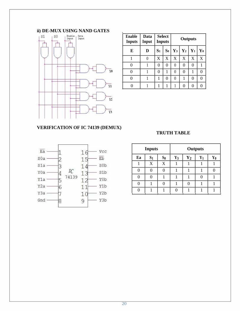
ii) DE-MUX USING NAND GATES
Enable
Inputs
Data
Input
Select
Inputs Outputs
E D S1 S0 Y3 Y2 Y1 Y0
1 0 X X X X X X
0 1 0 0 0 0 0 1
0 1 0 1 0 0 1 0
0 1 1 0 0 1 0 0
0 1 1 1 1 0 0 0
VERIFICATION OF IC 74139 (DEMUX)
TRUTH TABLE

21
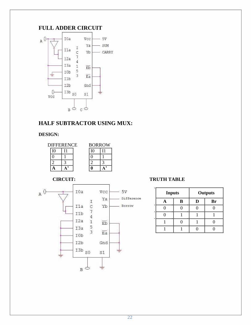
HALF ADDER USING MUX:
DESIGN: SUM CARRY
CIRCUIT:
FULL ADDER USING MUX:
DESIGN:
SUM I0 I1 I3 I3
0 1 2 3
4 5 6 7
A A’ A’ A
TRUTH TABLE
TRUTH TABLE
Input
s
Outputs
A B S C
0 0 0 0
0 1 1 0
1 0 1 0
1 1 0 1
CARRY
I0 I1 I3 I3
0 1 2 3
4 5 6 7
0 A A 1
Inputs Outputs
A B C S C
0 0 0 0 0
0 0 1 1 0
0 1 0 1 0
0 1 1 0 1
1 0 0 1 0
1 0 1 0 1
1 1 0 0 1
1 1 1 1 1
I0 I1
0 1
2 3
0 A
I0 I1
0 1
2 3
A A’
22
FULL ADDER CIRCUIT
HALF SUBTRACTOR USING MUX:
DESIGN:
DIFFERENCE BORROW
CIRCUIT: TRUTH TABLE
Inputs Outputs
A B D Br
0 0 0 0
0 1 1 1
1 0 1 0
1 1 0 0
I0 I1
0 1
2 3
0 A’
I0 I1
0 1
2 3
A A’
23
TRUTH
TABLE
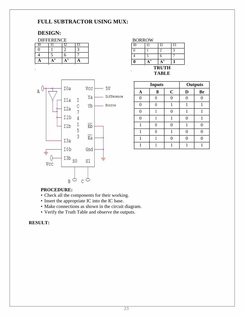
FULL SUBTRACTOR USING MUX:
DESIGN:
DIFFERENCE BORROW
Inputs Outputs
A B C D Br
0 0 0 0 0
0 0 1 1 1
0 1 0 1 1
0 1 1 0 1
1 0 0 1 0
1 0 1 0 0
1 1 0 0 0
1 1 1 1 1
PROCEDURE:
• Check all the components for their working.
• Insert the appropriate IC into the IC base.
• Make connections as shown in the circuit diagram.
• Verify the Truth Table and observe the outputs.
RESULT:
I0 I1 I2 I3
0 1 2 3
4 5 6 7
0 A’ A’ 1
I0 I1 I2 I3
0 1 2 3
4 5 6 7
A A’ A’ A

24
A<B = A B _ _
A=B = A B +AB
EXPERIMENT: 6
COMPARATORS
AIM: To realize One & Two Bit Comparator and study of 7485 magnitude comparator.
LEARNING OBJECTIVE: To learn about various applications of comparator
To learn and understand the working of IC 7485 magnitude comparator To learn to realize 8-bit comparator using 4-bit comparator
THEORY:
Magnitude Comparator is a logical circuit, which compares two signals A and B and generates three logical outputs, whether A > B, A = B, or A < B. IC 7485 is a high
speed 4-bit Magnitude comparator , which compares two 4-bit words . The A = B Input must be held high for proper compare operation.
COMPONENTS REQUIRED:
IC 7400, IC 7410, IC 7420, IC 7432, IC 7486, IC 7402, IC 7408, IC 7404, IC 7485, Patch Cords & IC Trainer Kit.
1) 1- BIT COMPARATOR TRUTH TABLE _
A>B = A B _
INPUTS OUTPUTS
A B A > B A = B A < B
0 0 0 1 0
0 1 0 0 1
1 0 1 0 0
1 1 0 1 0
2) 2- BIT COMPARATOR _ _ _ _
(A>B)= A1 B1 + A0 B1 B 0 + B 0 A1A0
(A=B) = (A0 ⊕ B0) (A1 ⊕ B1) − _ _ _
(A<B) = B1 A1 +B0 A1 A 0 + A 0B1B0

25
TRUTH TABLE
INPUTS OUTPUTS
A1 A0 B1 B0 A > B A = B A < B
0 0 0 0 0 1 0
0 0 0 1 0 0 1
0 0 1 0 0 0 1
0 0 1 1 0 0 1
0 1 0 0 1 0 0
0 1 0 1 0 1 0
0 1 1 0 0 0 1
0 1 1 1 0 0 1
1 0 0 0 1 0 0
1 0 0 1 1 0 0
1 0 1 0 0 1 0
1 0 1 1 0 0 1
1 1 0 0 1 0 0
1 1 0 1 1 0 0
1 1 1 0 1 0 0
1 1 1 1 0 1 0

26
26
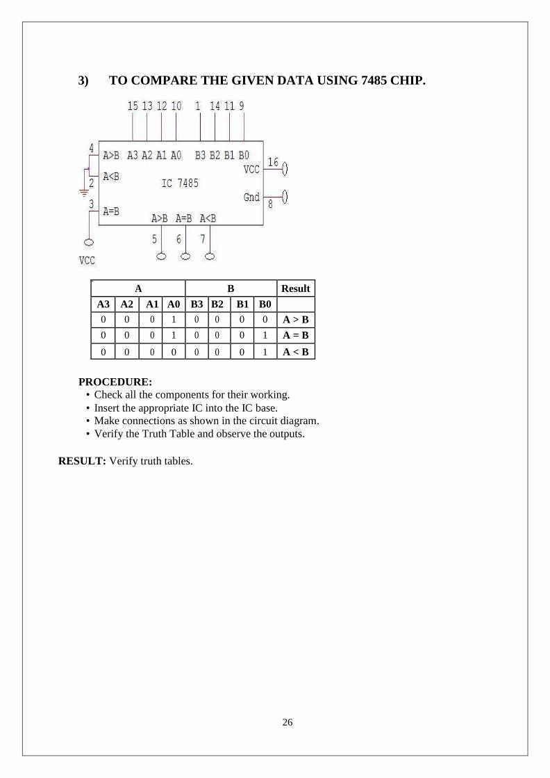
3) TO COMPARE THE GIVEN DATA USING 7485 CHIP.
A B Result
A3 A2 A1 A0 B3 B2 B1 B0
0 0 0 1 0 0 0 0 A > B
0 0 0 1 0 0 0 1 A = B
0 0 0 0 0 0 0 1 A < B
PROCEDURE:
• Check all the components for their working.
• Insert the appropriate IC into the IC base.
• Make connections as shown in the circuit diagram.
• Verify the Truth Table and observe the outputs.
RESULT: Verify truth tables.
27
EXPERIMENT 7
DECODER AND PRIORITY ENCODER
AIM: Implement the decoder circuit to drive LED and also implement the priority
encoder circuit.
LEARNING OBJECTIVE:
i) To learn about working principle of decoder and encoder
ii) To learn about various applications of decoder and encoder
iii) To learn and understand the working of IC 7447, IC74147.
COMPONENTS REQUIRED:
IC-7447, 74147, LED, Digital IC trainer kit and Patch cords.
THEORY:
IC – 74147 is a decimal to BCD priority encoder. The input decimal number 0 through
9 are converted to its equivalent Binary Coded Decimal (BCD) number.
Encoders are inverse of decoders. That is, generally decoder has n-inputs and 2n
outputs and generally encoder has 2n inputs and n outputs. E.g. When input n = 3 for
decoder, 2n = 8 outputs, hence it is called 3 to 8 line decoder, and BCD to seven segment
decoder has 4 – inputs and 10 (0-9) outputs, Octal – to – binary encoder has 23
= 8 inputs and only 3 binary outputs, and decimal – to –BCD encoder has 10 (0-9)
inputs and 4- BCD outputs, which has application in digital systems.
The Priority encoder is one, the output of which always corresponds to the highest
order inputs.e.g. If the input is given simultaneously are 4 and 6, the output corresponds
to 6 only, because 6 has higher priority than 4. One can verify this from the truth table of
decimal – to BCD encoder.
When all the inputs are HIGH, active LOW outputs also HIGH and is equal to BCD
0,to obtain normal BCD output, use inverter as shown in the circuit diagram. When the
last input i.e. Input (is LOW the output of encoder is BCD = 1 0 0 1, equivalent of
decimal 9 (Inverted Output).
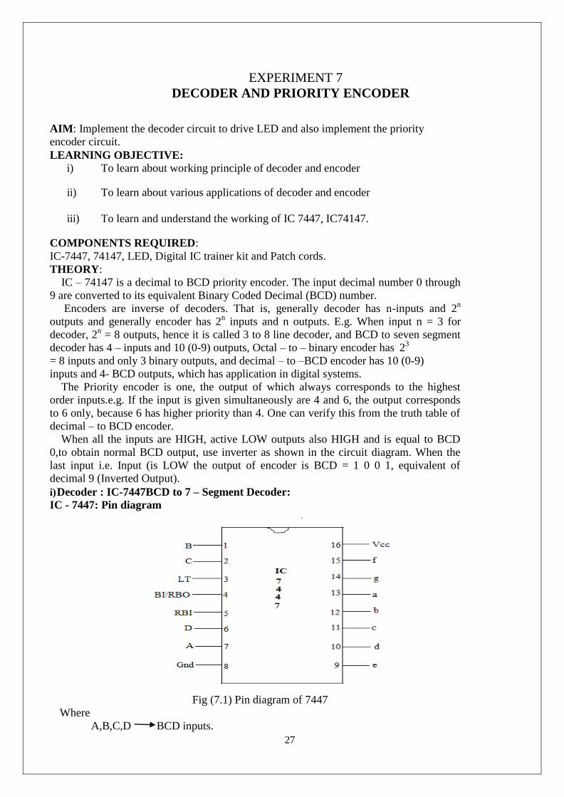
i) Decoder : IC-7447BCD to 7 – Segment Decoder:
IC - 7447: Pin diagram
Where
Fig (7.1) Pin diagram of 7447
A,B,C,D BCD inputs.

28
a-f Active LOW outputs of decoder that drives LED.
IC-7447/46 is a BCD to 7 – Segment Decoder, this type of decoder takes BCD code as input and provides
output to drive seven segment display devices in order to produce decimal data.
29
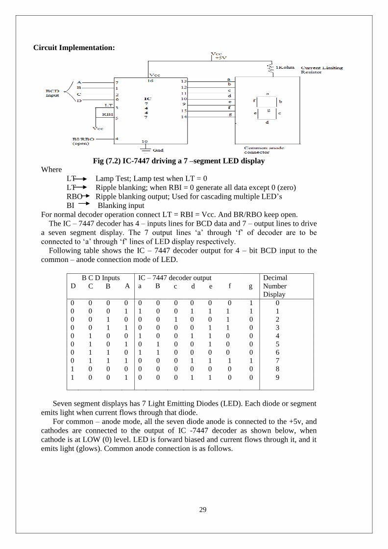
Circuit Implementation:
Where
Fig (7.2) IC-7447 driving a 7 –segment LED display
LT Lamp Test; Lamp test when LT = 0
LT Ripple blanking; when RBI = 0 generate all data except 0 (zero)
RBO Ripple blanking output; Used for cascading multiple LED’s
BI Blanking input
For normal decoder operation connect LT = RBI = Vcc. And BR/RBO keep open.
The IC – 7447 decoder has 4 – inputs lines for BCD data and 7 – output lines to drive
a seven segment display. The 7 output lines ‘a’ through ‘f’ of decoder are to be
connected to ‘a’ through ‘f’ lines of LED display respectively.
Following table shows the IC – 7447 decoder output for 4 – bit BCD input to the
common – anode connection mode of LED.
D B C D
C
Inputs
B
A IC a
– 7447 B
decoder output
c d e
f
g Decimal
Number
Display
0 0 0 0 0 0 0 0 0 0 1 0
0 0 0 1 1 0 0 1 1 1 1 1
0 0 1 0 0 0 1 0 0 1 0 2
0 0 1 1 0 0 0 0 1 1 0 3
0 1 0 0 1 0 0 1 1 0 0 4
0 1 0 1 0 1 0 0 1 0 0 5
0 1 1 0 1 1 0 0 0 0 0 6
0 1 1 1 0 0 0 1 1 1 1 7
1 0 0 0 0 0 0 0 0 0 0 8
1 0 0 1 0 0 0 1 1 0 0 9
Seven segment displays has 7 Light Emitting Diodes (LED). Each diode or segment
emits light when current flows through that diode.
For common – anode mode, all the seven diode anode is connected to the +5v, and
cathodes are connected to the output of IC -7447 decoder as shown below, when
cathode is at LOW (0) level. LED is forward biased and current flows through it, and it
emits light (glows). Common anode connection is as follows.
30
Fig (7.3) Common – anode connection for seven segments LED
For example to display 8, all the seven segment i.e. all seven LED’s should glow. To
make these LED’s to glow (conduct), it must be forward biased. All the LED’s
conducts when a = b = c = d = e = f = g = 0V. See table
ii) Priority Encoder:
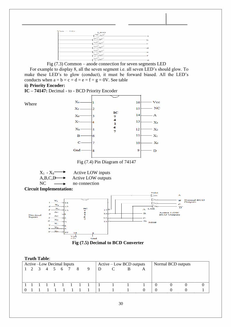
IC – 74147: Decimal - to - BCD Priority Encoder
Where
Fig (7.4) Pin Diagram of 74147
X1 - X9 Active LOW inputs
A,B,C,D Active LOW outputs
NC no connection
Circuit Implementation:
Fig (7.5) Decimal to BCD Converter
Truth Table:
Active –Low Decimal Inputs
1 2 3 4 5 6 7 8 9 Active
D
– Low BCD outputs
C B A
Normal BCD outputs
1 1 1 1 1 1 1 1 1 1 1 1 1 0 0 0 0
0 1 1 1 1 1 1 1 1 1 1 1 0 0 0 0 1

30
X 0 1 1 1 1 1 1 1 1 1 0 1 0 0 1 0
X X 0 1 1 1 1 1 1 1 1 0 0 0 0 1 1
X X X 0 1 1 1 1 1 1 0 1 1 0 1 0 0
X X X X 0 1 1 1 1 1 0 1 0 0 1 0 1
X X X X X 0 1 1 1 1 0 0 1 0 1 1 0 X X X X X X 0 1 1 1 0 0 0 0 1 1 1
X X X X X X X 0 1 0 1 1 1 1 0 0 0
X X X X X X X X 0 0 1 1 0 1 0 0 1
PROCEDURE:
1. Connections are made as per the circuit diagram. 2. Apply inputs as shown in the truth table and verify the corresponding BCD outputs.
Apply the BCD inputs and verify the corresponding decimal outputs for decoder.
3. Switch off – power supply and disconnect the circuit.
RESULT:

31
EXPERIMENT 8 STUDY OF FLIPFLOPS
AIM: To implement the circuit and to verify the truth table of the following Flip-Flops.
LEARNING OBJECTIVE:
i) To learn about various Flip-Flops. ii) To learn and understand the working of Master slave FF.
COMPONENTS REQUIRED:
7485, 7408, 8411, 7421, 7432, digital IC Trainer Kit, Patch Chord.
THEORY:
Basically Flip-Flops are the bistable multi vibrators that stores logic 1 and logic 0.Shift registers,
memory, and counters are built by using Flip – Flops. Any complex sequential machines are build using
Flip – Flops. Sequential circuit (machine) output depends on the present state and input applied at that
instant.
Mealy Machine is one whose output depends on both the present state and the input. Moore
machines one whose output depends only on the present state of the sequential circuit. Note that the
truth table of J – K Flip – Flop is same as the Master – Slave.
J – K Flip Flop and they must be remain same because IC – 7476is –ve edge trigged flip – flop and
we know that race around condition is eliminated by edge triggered flip – flop. Another way of
eliminating race around condition is by using Master – Slave J –K Flip – Flop. When J = K = 1 (logic
HIGH), J – K Flip – Flop changes output many times for single clock pulse, it is Smaller than width of
the clock pulse.
32
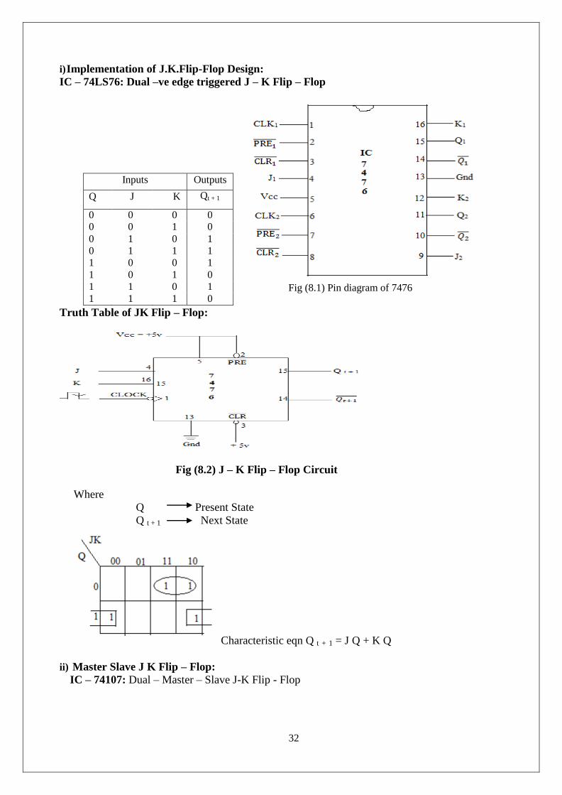
i) Implementation of J.K.Flip-Flop Design:
IC – 74LS76: Dual –ve edge triggered J – K Flip – Flop
Fig (8.1) Pin diagram of 7476
Truth Table of JK Flip – Flop:
Where
Fig (8.2) J – K Flip – Flop Circuit
Q Present State
Q t + 1 Next State
Characteristic eqn Q t + 1 = J Q + K Q
ii) Master Slave J K Flip – Flop:
IC – 74107: Dual – Master – Slave J-K Flip - Flop
Inputs Outputs
Q J K Qt + 1
0 0 0 0 0 0 1 0
0 1 0 1
0 1 1 1
1 0 0 1
1 0 1 0
1 1 0 1
1 1 1 0

33
Fig (8.3) Pin diagram
Circuit Implementation:
Fig (8.4) Master – Slave J –K Flip – Flop Circuit.
Truth Table of Master – Slave – JK Flip – Flop:
Q Present state
Qt + 1 Next state
Where
Characteristic eqn Q t + 1 = J Q + K Q
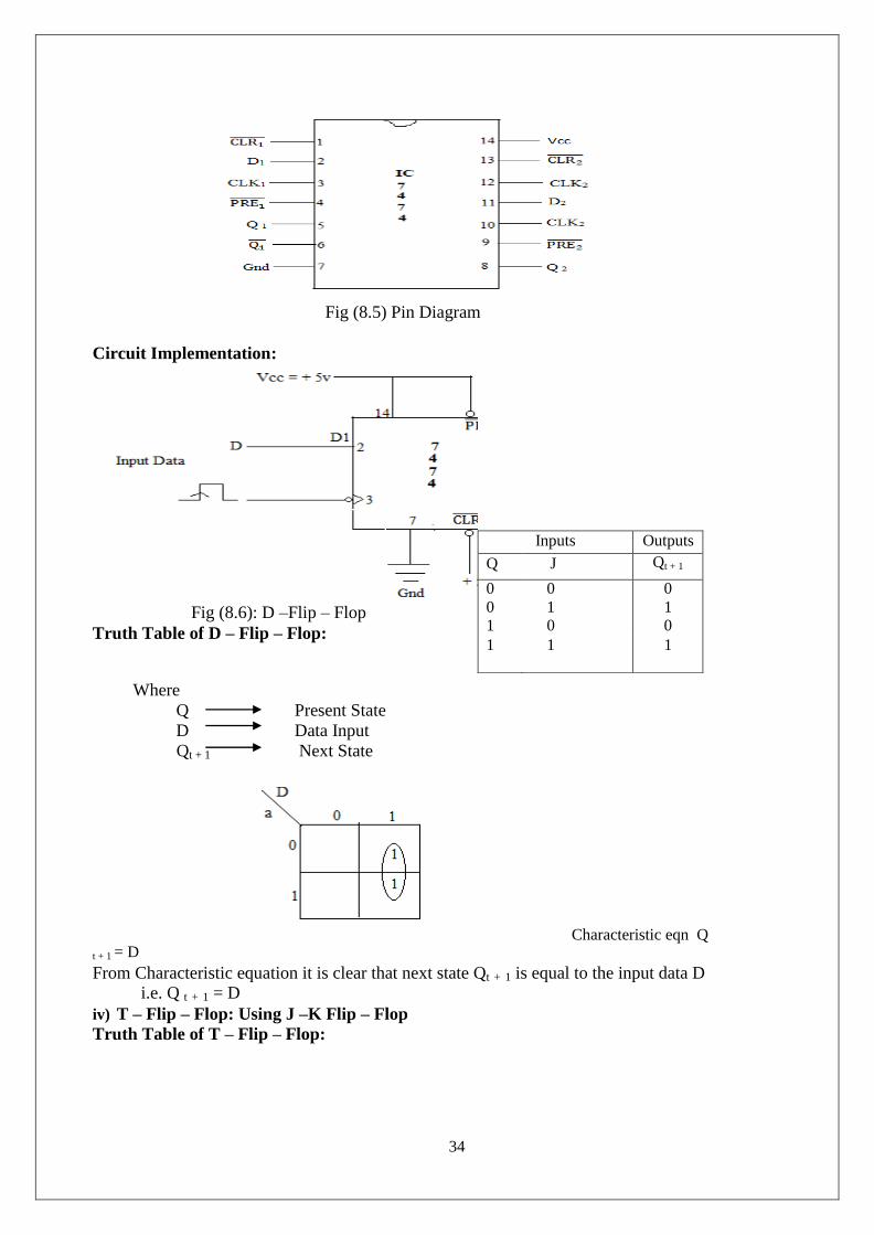
iii) D – Flip – Flop:
IC – 7474: Dual + ve edge triggered D- Flip Flop :
Inputs Outputs
Q J K Qt + 1
0 0 0 0 0 0 1 0
0 1 0 1
0 1 1 1
1 0 0 1
1 0 1 0
1 1 0 1
1 1 1 0
34
Fig (8.5) Pin Diagram
Circuit Implementation:
Fig (8.6): D –Flip – Flop
Truth Table of D – Flip – Flop:
Where
Q Present State
D Data Input
Qt + 1 Next State
Characteristic eqn Q
t + 1 = D
From Characteristic equation it is clear that next state Qt + 1 is equal to the input data D i.e. Q t + 1 = D
iv) T – Flip – Flop: Using J –K Flip – Flop
Truth Table of T – Flip – Flop:
Inputs Outputs
Q J Qt + 1
0 0 0
0 1 1 1 0 0
1 1 1

35
Fig (8.7) : T – Flip - Flop Circuit
Where
Q Present State
D Data Input
Characteristic eqn Q t + 1 = DT + Q T (Ex – OR)
The next state of T Flip Flop is equal to Ex –OR of Present State (Q) and T input.
PROCEDURE:
1) Connections are made as per the circuit diagram.
2) Apply the –ve edge triggered, +ve edge triggered and level sensitive clock pulses
as required.
3) Verify the truth table of all the Flip – Flops.
4) Switch - off the power supply and disconnect the circuit.
RESULT:
Inputs Outputs
Q J Qt + 1
0 0 0
0 1 1
1 0 0
1 1 1

36
EXPERIMENT: 9
STUDY OF COUNTERS
I. STUDY OF ASYNCHRONOUS COUNTER
AIM: To design and test 3-bit binary asynchronous counter using flip-flop IC
7476 for the given sequence.
LEARNING OBJECTIVE:
To learn about Asynchronous Counter and its application
To learn the design of asynchronous up counter and down counter
COMPONENTS REQUIRED:
IC 7476, Patch Cords & IC Trainer Kit
THEORY:
A counter in which each flip-flop is triggered by the output goes to previous
flip-flop. As all the flip-flops do not change state simultaneously spike occur at the
output. To avoid this, strobe pulse is required. Because of the propagation delay
the operating speed of asynchronous counter is low. Asynchronous counter are
easy and simple to construct.
Design:
MOD-8 UP COUNTER

37
MOD_5 UP COUNTER
CIRCUIT DIAGRAM:
MOD-8 DOWN COUNTER
CIRCUIT DIAGRAM:
38
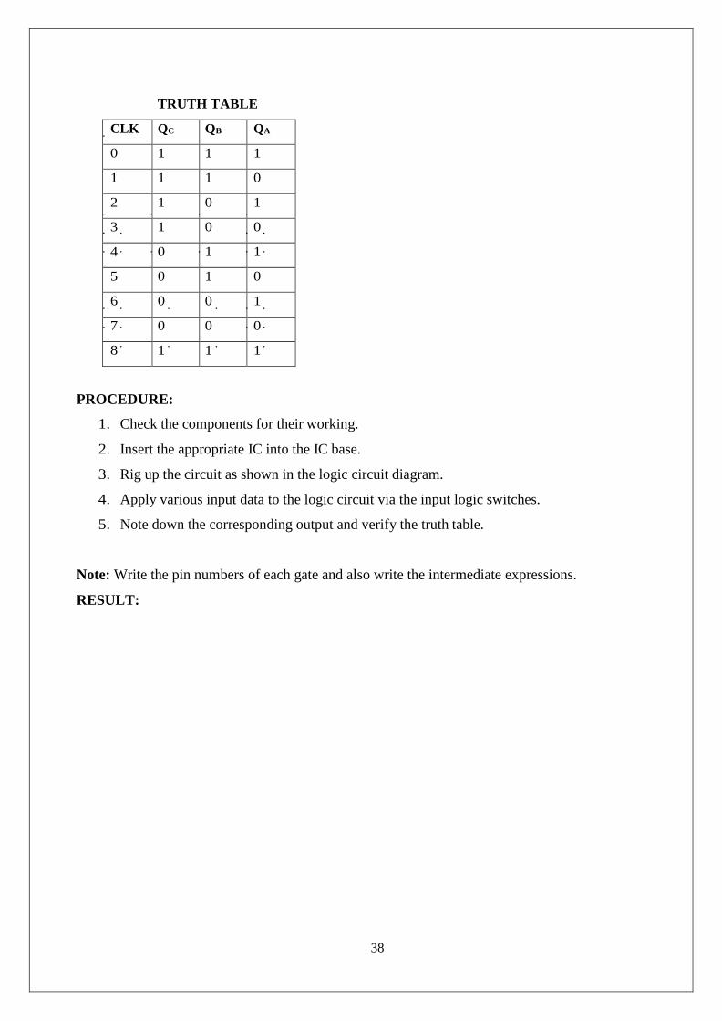
TRUTH TABLE
CLK QC QB QA
0 1 1 1
1 1 1 0
2 1 0 1
3 1 0 0
4 0 1 1
5 0 1 0
6 0 0 1
7 0 0 0
8 1 1 1
PROCEDURE:
1. Check the components for their working.
2. Insert the appropriate IC into the IC base.
3. Rig up the circuit as shown in the logic circuit diagram.
4. Apply various input data to the logic circuit via the input logic switches.
5. Note down the corresponding output and verify the truth table.
Note: Write the pin numbers of each gate and also write the intermediate expressions.
RESULT:
39
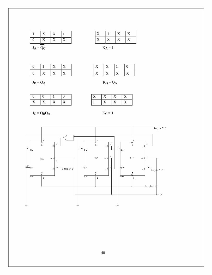
II. SYNCHRONOUS COUNTERS
AIM: To design and test 3-bit binary synchronous counter using flip-flop IC 7476 for the
given sequence.
LEARNING OBJECTIVE:
To learn about synchronous Counter and its application To learn the design of synchronous counter
COMPONENTS REQUIRED:
IC 7476, Patch Cords & IC Trainer Kit
THEORY:
A counter in which each flip-flop is triggered by the output goes to previous flip- flop. As all the flip-flops do not change states simultaneously in asynchronous counter, spike occur at the output. To avoid this, strobe pulse is required. Because of the propagation delay the operating speed of asynchronous counter is low. This problem can be solved by triggering all the flip-flops in synchronous with the clock signal and such counters are called synchronous counters.
Design:
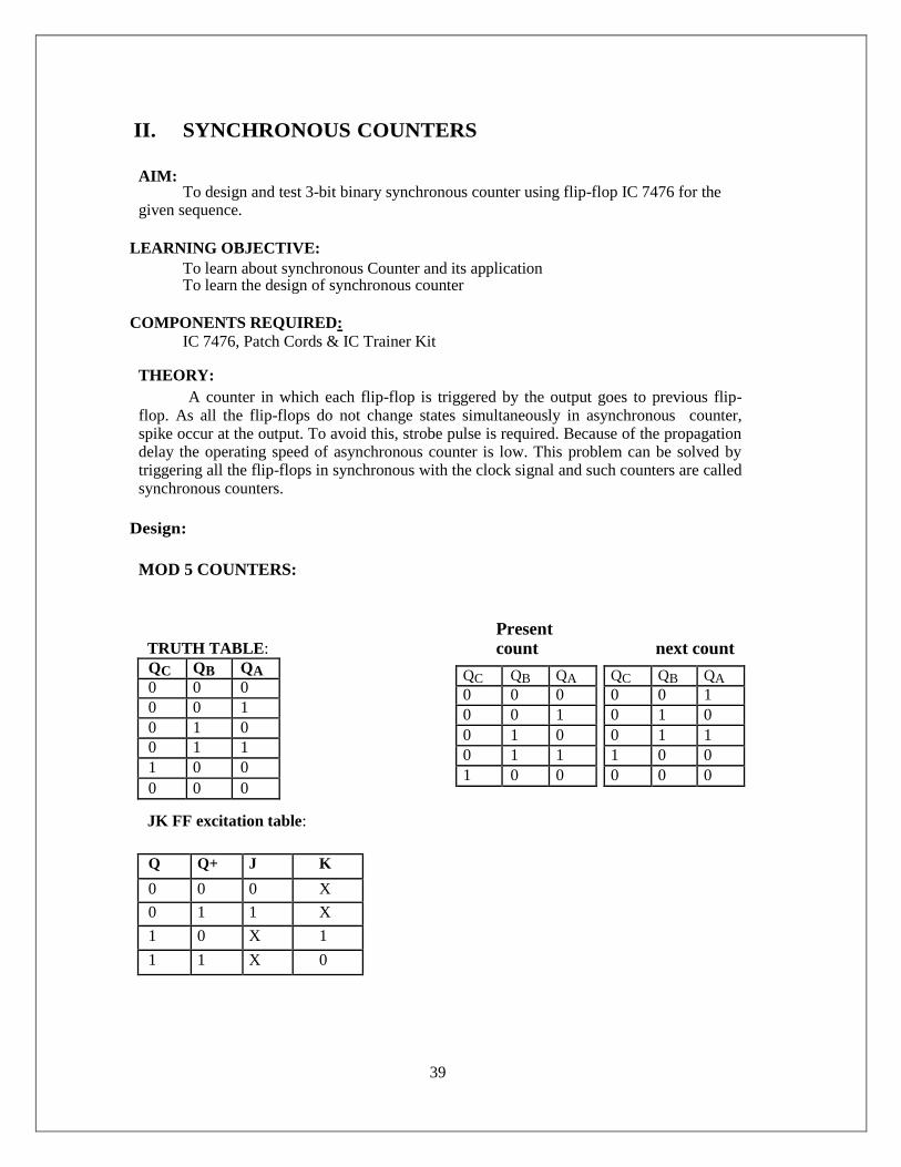
MOD 5 COUNTERS:
TRUTH TABLE:
QC QB QA
0 0 0
0 0 1
0 1 0
0 1 1
1 0 0
0 0 0
JK FF excitation table:
Present count next count
Q Q+ J K
0 0 0 X
0 1 1 X
1 0 X 1
1 1 X 0
QC QB QA
0 0 1
0 1 0
0 1 1
1 0 0
0 0 0
QC QB QA
0 0 0
0 0 1
0 1 0
0 1 1
1 0 0
40
0 1 X X
0 X X X
X X 1 0
X X X X
0 0 1 0
X X X X
X X X X
1 X X X
JA = QC KA = 1
JB = QA KB = QA
JC = QBQA KC = 1
X 1 X X
X X X X
1 X X 1
0 X X X
41
0 1 X X
X 1 X X
X X 1 0
X X 1 0
0 0 1 0
X X X X
X X X X
0 0 1 0
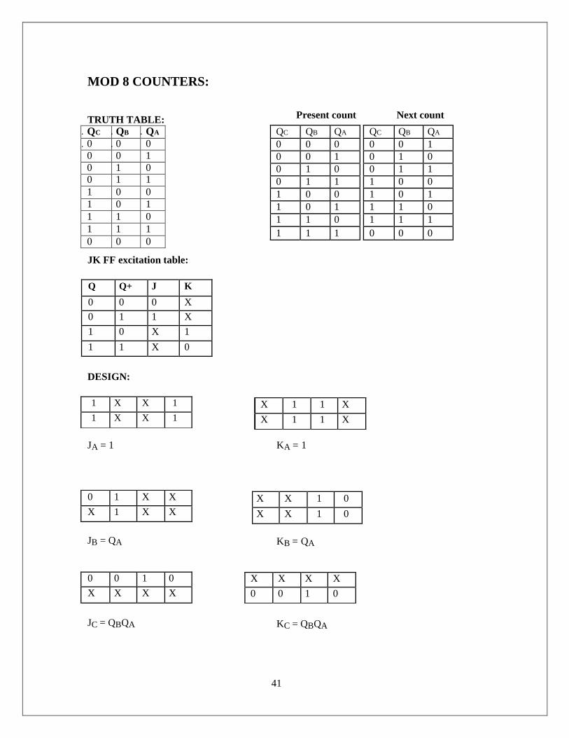
MOD 8 COUNTERS:
TRUTH TABLE:
QC QB QA
0 0 0
0 0 1
0 1 0
0 1 1
1 0 0
1 0 1
1 1 0
1 1 1
0 0 0
JK FF excitation table:
Q Q+ J K
0 0 0 X
0 1 1 X
1 0 X 1
1 1 X 0
DESIGN:
Present count
QC QB QA
0 0 0
0 0 1
0 1 0
0 1 1
1 0 0
1 0 1
1 1 0
1 1 1
Next count
QC QB QA
0 0 1
0 1 0
0 1 1
1 0 0
1 0 1
1 1 0
1 1 1
0 0 0
JA = 1 KA = 1
JB = QA KB = QA
JC = QBQA KC = QBQA
X 1 1 X
X 1 1 X
1 X X 1
1 X X 1

42
PROCEDURE:
1. Check the components for their working.
2. Insert the appropriate IC into the IC base.
3. Rig up the circuit as shown in the logic circuit diagram.
4. Apply various input data to the logic circuit via the input logic switches.
5. Note down the corresponding output and verify the truth table.
Note: Write the pin numbers of each gate and also write the intermediate expressions.
RESULT:

43
III. PRESETTABLE 4-BIT BINARY UP/DOWN COUNTER
AIM: To design IC 74193 as a up/down counter
COMPONENTS REQUIRED:
IC 74193, Patch Cords & IC Trainer Kit
PIN DETAILS OF IC 74193
1. P1,P2,P3 and P0 are parallel data inputs
2. Q0,Q1,Q2 and Q3 are flip-flop outputs
3. MR: Asynchronous master reset
4. PL: Asynchronous parallel load(active low) input
5. TCd : Terminal count-down output
6. TCu : Terminal count-up output
44
CLK QD QC QB QA
0 0 0 0 0
1 0 0 0 1
2 0 0 1 0
3 0 0 1 1
4 0 1 0 0
5 0 1 0 1
6 0 1 1 0
7 0 1 1 1
8 1 0 0 0
9 1 0 0 1
10 1 0 1 0
11 1 0 1 1
12 1 1 0 0
13 1 1 0 1
14 1 1 1 0
15 1 1 1 1
16 0 0 0 0
CLK QD QC QB QA
0 1 1 1 1
1 1 1 1 0
2 1 1 0 1
3 1 1 0 0
4 1 0 1 1
5 1 0 1 0
6 1 0 0 1
7 1 0 0 0
8 0 1 1 1
9 0 1 1 0
10 0 1 0 1
11 0 1 0 0
12 0 0 1 1
13 0 0 1 0
14 0 0 0 1
15 0 0 0 0
16 1 1 1 1
Up counter Down counter
Design up/ down counter using presettable counter
CIRCUIT DIAGRAM

45
PROCEDURE:
1. Check the components for their working.
2. Insert the appropriate IC into the IC base.
3. Rig up the circuit as shown in the logic circuit diagram.
4. Apply the parallel input to p0 to p3 and Give the Load pin to logic LOW.
5. To start counting connect Load input to logic HIGH.
6. Apply the clock pulse to observe the output.( For up-counter make clock down to
be at logic 1 and give the clock input to Clock up input, for down counter make
clock up to be at logic 1 and give the clock input to Clock down input)
Note:
1. For up-counter make clock down to be at logic 1 and give the clock input to
Clock up input.
2. For down counter make clock up to be at logic 1 and give the clock input to
Clock down input
3. Write the pin numbers of each gate and also write the intermediate expressions.
RESULT:

46
IV. STUDY OF 7490 BCD COUNTER
AIM: To design IC 7490 as a decade counter with BCD count sequence
COMPONENTS REQUIRED:
IC 7490, Patch Cords & IC Trainer Kit
DECADE COUNTER:
TRUTH TABLE: QD QC QB QA
0 0 0 0
0 0 0 1
0 0 1 0
0 0 1 1
0 1 0 0
0 1 0 1
0 1 1 0
0 1 1 1
1 0 0 0
1 0 0 1
0 0 0 0
PROCEDURE:
1. Check the components for their working.
2. Insert the appropriate IC into the IC base.
3. Rig up the circuit as shown in the logic circuit diagram.
4. Apply various input data to the logic circuit via the input logic switches.
5. Note down the corresponding output and verify the truth table.

47
Note: Write the pin numbers of each gate and also write the intermediate
expressions.
RESULT:

48
QA QB QC QD f
1 1 1 1 0
0 1 1 1 0
0 0 1 1 0
0 0 0 1 1
1 0 0 0 0
0 1 0 0 0
0 0 1 0 1
1 0 0 1 1
1 1 0 0 0
0 1 1 0 1
1 0 1 1 0
0 1 0 1 1
1 0 1 0 1
1 1 0 1 1
1 1 1 0 1
EXPERIMENT 10
SEQUENCE GENERATOR USING D FLIP FLOP(IC 7474)
AIM: Design a Sequence Generator for the given Sequence 100010011010111.
COMPONENTS REQUIRED: Shift register (7495) , Ex-OR (7486) , NANDgate(3i/ps) (7410) , Trainer Kit,
Patch Cords.
Theory:- Find required number of flip-flops .
Truth Table Simplification
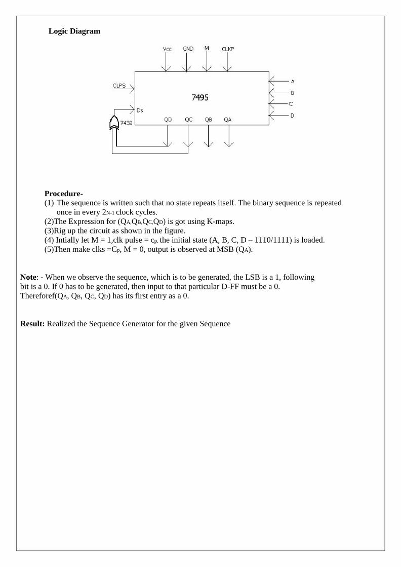
Logic Diagram
Procedure-
(1) The sequence is written such that no state repeats itself. The binary sequence is repeated
once in every 2N-1 clock cycles.
(2)The Expression for (QA,QB,QC,QD) is got using K-maps.
(3)Rig up the circuit as shown in the figure.
(4) Intially let M = 1,clk pulse = cp, the initial state (A, B, C, D – 1110/1111) is loaded.
(5)Then make clks =Cp, M = 0, output is observed at MSB (QA).
Note: - When we observe the sequence, which is to be generated, the LSB is a 1, following
bit is a 0. If 0 has to be generated, then input to that particular D-FF must be a 0.
Thereforef(QA, QB, QC, QD) has its first entry as a 0.
Result: Realized the Sequence Generator for the given Sequence

VIVA QUESTIONS
1. Differentiate BCD & Excess 3 code
2. What is BCD?
3. What is the base for Binary?
4. How will you convert Binary to Gray?
5. What is Gray Code?
6. Give the conversion process of Excess 3 to BCD
7. What are the logic gates used in converting Gray code to Binary?
8. What is the need of code converters?
9. How will you design Code converters?
10. What is the difference between Positive and Negative logic?
11. What are Analog Systems? Give Examples.
12. What are Digital Systems? Give Examples.
13. Mention the disadvantages of Analog systems over Digital systems.
14. Explain Boolean algebra.
15. State Principle of Duality.
16. State De – morgan’s Law.
17. Define Positive Logic and Negative Logic.
18. Define Literal.
19. Define MINTERM and MAX TERM.
20. Which are the basic gates and universal gates.
21. Define combinational circuit with example.
22. Define Sequential circuit with example.
23. Explain the significance of a Don’t care function.
24. What are Prime Implicants?
Related Documents