NJIT ECE271 Dr.Serhiy Levkov Topic 7 - 1 Topic 7 Digital Circuits Intro to Digital Electronics ECE 271 Electronic Circuits I

NJIT ECE271 Dr.Serhiy Levkov Topic 7 - 1 Topic 7 Digital Circuits Intro to Digital Electronics ECE 271 Electronic Circuits I.
Dec 17, 2015
Welcome message from author
This document is posted to help you gain knowledge. Please leave a comment to let me know what you think about it! Share it to your friends and learn new things together.
Transcript

NJIT ECE271 Dr.Serhiy Levkov Topic 7 - 1
Topic 7 Digital Circuits
Intro to Digital Electronics
ECE 271
Electronic Circuits I

NJIT ECE271 Dr.Serhiy Levkov
Brief History of Digital Electronics
• Digital electronics can be found in many applications in the form of microprocessors, microcontrollers, PCs, DSPs, and an uncountable number of other systems.
• The historic development of design of digital circuits:– resistor-transistor logic (RTL) – diode-transistor logic (DTL) – transistor-transistor logic (TTL) – emitter-coupled logic (ECL) – NMOS – complementary MOS (CMOS)
Topic 7 - 2

NJIT ECE271 Dr.Serhiy Levkov
Digital Binary Logic• Digital electronics represent signals by discrete bands of analog levels, rather than
by a continuous range.
Topic 7 - 3

NJIT ECE271 Dr.Serhiy Levkov
Digital Binary Logic• Digital electronics represent signals by discrete bands of analog levels, rather than
by a continuous range.
• All levels within a band represent the same signal state.
• Small changes to the analog signal levels due to manufacturing tolerance, or noise do not leave the discrete envelope, and as a result are ignored by signal state sensing circuitry.
Topic 7 - 4
NJIT ECE271 Dr.Serhiy Levkov
Digital Binary Logic• Digital electronics represent signals by discrete bands of analog levels, rather than
by a continuous range.
• All levels within a band represent the same signal state.
• Small changes to the analog signal levels due to manufacturing tolerance, or noise do not leave the discrete envelope, and as a result are ignored by signal state sensing circuitry.
• Binary logic is the most common style of digital logic.
• The signal is either a 0 (low, false) or a 1 (high, true) - Positive Logic Convention
Topic 7 - 5

NJIT ECE271 Dr.Serhiy Levkov
Digital Binary Logic• Digital electronics represent signals by discrete bands of analog levels, rather than
by a continuous range.
• All levels within a band represent the same signal state.
• Small changes to the analog signal levels due to manufacturing tolerance, or noise do not leave the discrete envelope, and as a result are ignored by signal state sensing circuitry.
• Binary logic is the most common style of digital logic.
• The signal is either a 0 (low, false) or a 1 (high, true) - Positive Logic Convention
• Mathematical representation of logical operations is Boolean algebra: set of operations (NOT, AND, OR, NAND, NOR, etc.) with binary or logical elements.
• • To perform general logical operations, a logic family must contain NOT and at least
one another function of two inputs OR or AND.
Topic 7 - 6

NJIT ECE271 Dr.Serhiy Levkov
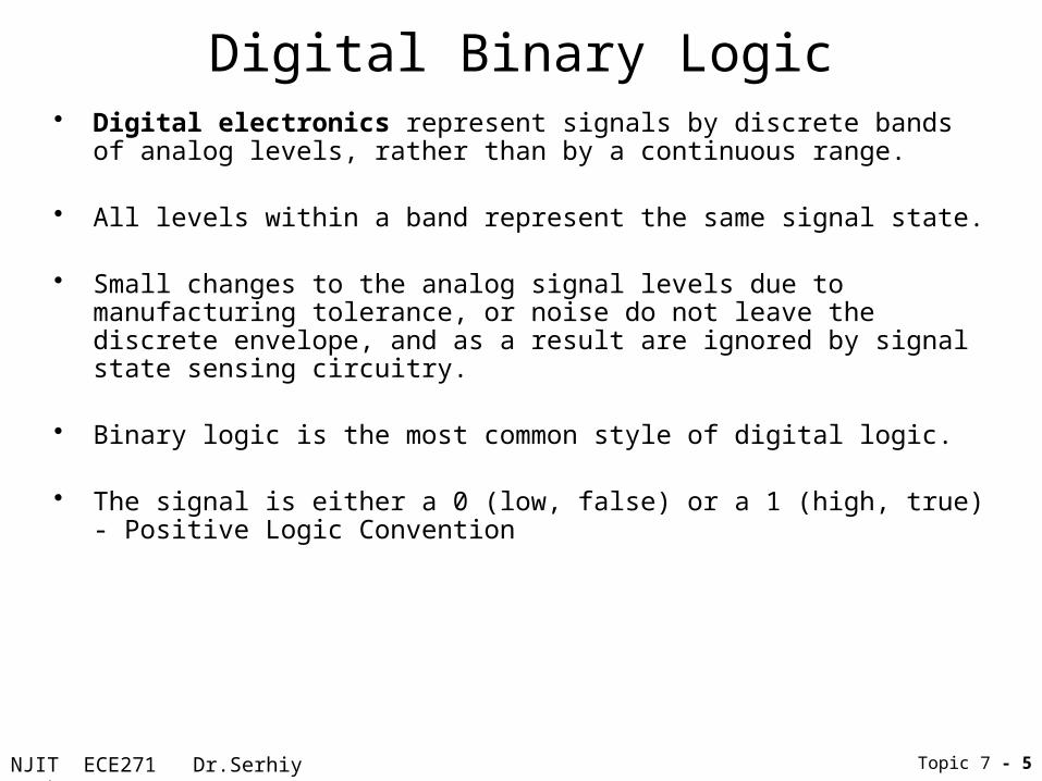
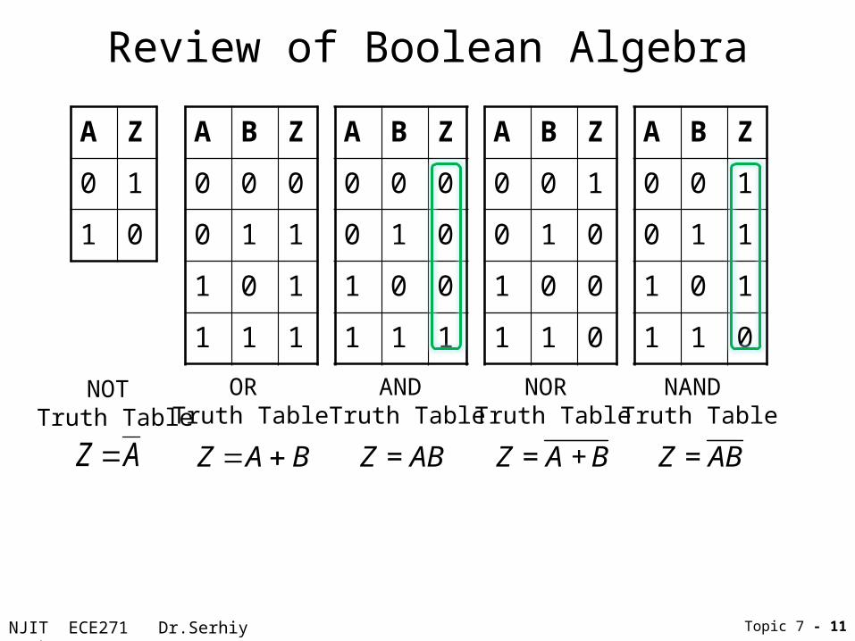
Review of Boolean Algebra
A Z
0 1
1 0
A B Z
0 0 0
0 1 1
1 0 1
1 1 1
A B Z
0 0 0
0 1 0
1 0 0
1 1 1
NOT Truth Table
OR Truth Table
AND Truth Table
A B Z
0 0 1
0 1 0
1 0 0
1 1 0
A B Z
0 0 1
0 1 1
1 0 1
1 1 0
NOR Truth Table
NAND Truth Table
Z A
Z A B Z = AB Z = A + B Z = AB
Topic 7 - 7
NJIT ECE271 Dr.Serhiy Levkov
Review of Boolean Algebra
A Z
0 1
1 0
A B Z
0 0 0
0 1 1
1 0 1
1 1 1
A B Z
0 0 0
0 1 0
1 0 0
1 1 1
NOT Truth Table
OR Truth Table
AND Truth Table
A B Z
0 0 1
0 1 0
1 0 0
1 1 0
A B Z
0 0 1
0 1 1
1 0 1
1 1 0
NOR Truth Table
NAND Truth Table
Z A
Z A B Z = AB Z = A + B Z = AB
Topic 7 - 8

NJIT ECE271 Dr.Serhiy Levkov
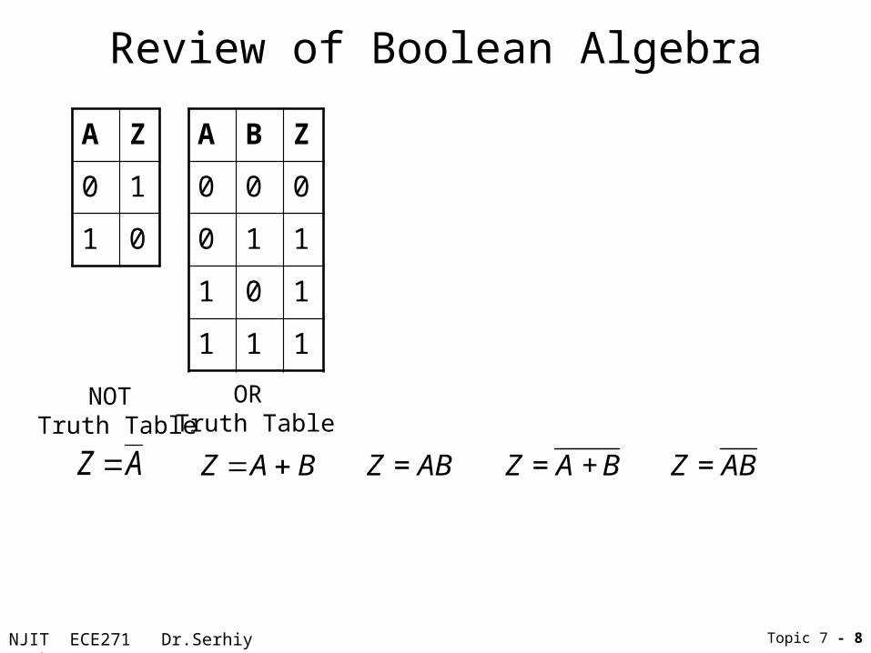
Review of Boolean Algebra
A Z
0 1
1 0
A B Z
0 0 0
0 1 1
1 0 1
1 1 1
A B Z
0 0 0
0 1 0
1 0 0
1 1 1
NOT Truth Table
OR Truth Table
AND Truth Table
A B Z
0 0 1
0 1 0
1 0 0
1 1 0
A B Z
0 0 1
0 1 1
1 0 1
1 1 0
NOR Truth Table
NAND Truth Table
Z A
Z A B Z = AB Z = A + B Z = AB
Topic 7 - 9
NJIT ECE271 Dr.Serhiy Levkov
Review of Boolean Algebra
A Z
0 1
1 0
A B Z
0 0 0
0 1 1
1 0 1
1 1 1
A B Z
0 0 0
0 1 0
1 0 0
1 1 1
NOT Truth Table
OR Truth Table
AND Truth Table
A B Z
0 0 1
0 1 0
1 0 0
1 1 0
A B Z
0 0 1
0 1 1
1 0 1
1 1 0
NOR Truth Table
NAND Truth Table
Z A
Z A B Z = AB Z = A + B Z = AB
Topic 7 - 10
NJIT ECE271 Dr.Serhiy Levkov
Review of Boolean Algebra
A Z
0 1
1 0
A B Z
0 0 0
0 1 1
1 0 1
1 1 1
A B Z
0 0 0
0 1 0
1 0 0
1 1 1
NOT Truth Table
OR Truth Table
AND Truth Table
A B Z
0 0 1
0 1 0
1 0 0
1 1 0
A B Z
0 0 1
0 1 1
1 0 1
1 1 0
NOR Truth Table
NAND Truth Table
Z A
Z A B Z = AB Z = A + B Z = AB
Topic 7 - 11

NJIT ECE271 Dr.Serhiy Levkov
Review of Boolean Algebra
A Z
0 1
1 0
A B Z
0 0 0
0 1 1
1 0 1
1 1 1
A B Z
0 0 0
0 1 0
1 0 0
1 1 1
NOT Truth Table
OR Truth Table
AND Truth Table
A B Z
0 0 1
0 1 0
1 0 0
1 1 0
A B Z
0 0 1
0 1 1
1 0 1
1 1 0
NOR Truth Table
NAND Truth Table
Z A
Z A B Z = AB Z = A + B Z = AB
Topic 7 - 12
De Morgan's laws
NJIT ECE271 Dr.Serhiy Levkov
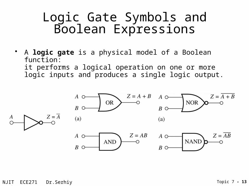
Logic Gate Symbols and Boolean Expressions
Topic 7 - 13
• A logic gate is a physical model of a Boolean function: it performs a logical operation on one or more logic inputs and produces a single logic output.

NJIT ECE271 Dr.Serhiy Levkov
Logic Gates: AND
Topic 7 - 14
A = 0 , B = 0 both diodes are forward biased both diodes conduct out is LOW 0.
The simples gates are AND and OR. They can be built from switches or using the simplest form of electronic logic - diode logic.

NJIT ECE271 Dr.Serhiy Levkov
Logic Gates: AND
Topic 7 - 15
A = 0 , B = 0 both diodes are forward biased both diodes conduct out is LOW 0.
A = 0 , B = 1 DB is reverse biased does not conduct, DA is forward biased conducts out is LOW 0.
The simples gates are AND and OR. They can be built from switches or using the simplest form of electronic logic - diode logic.
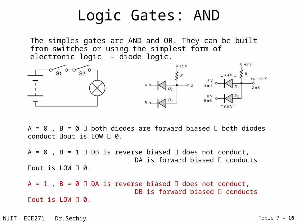
NJIT ECE271 Dr.Serhiy Levkov
Logic Gates: AND
Topic 7 - 16
A = 0 , B = 0 both diodes are forward biased both diodes conduct out is LOW 0.
A = 0 , B = 1 DB is reverse biased does not conduct, DA is forward biased conducts out is LOW 0.
A = 1 , B = 0 DA is reverse biased does not conduct, DB is forward biased conducts out is LOW 0.
The simples gates are AND and OR. They can be built from switches or using the simplest form of electronic logic - diode logic.

NJIT ECE271 Dr.Serhiy Levkov
Logic Gates: AND
Topic 7 - 17
A = 0 , B = 0 both diodes are forward biased both diodes conduct out is LOW 0.
A = 0 , B = 1 DB is reverse biased does not conduct, DA is forward biased conducts out is LOW 0.
A = 1 , B = 0 DA is reverse biased does not conduct, DB is forward biased conducts out is LOW 0.
A = 1 , B = 1 both diodes are reverse biased both the diodes do not conduct out is HIGH 1.
The simples gates are AND and OR. They can be built from switches or using the simplest form of electronic logic - diode logic.

NJIT ECE271 Dr.Serhiy Levkov
Logic Gates: OR
Topic 7 - 18
A = 0 , B = 0 both diodes are reverse biased does not conduct out is LOW 0.
A = 0 , B = 1 DA is reverse biased does not conduct, DB is forward biased conducts out is HIGH 1.
A = 1 , B = 0 DB is reverse biased does not conduct, DA is forward biased conducts out is HIGH 1.
A = 1 , B = 1 both diodes are reverse biased both the diodes conduct out is HIGH 1.

NJIT ECE271 Dr.Serhiy Levkov
Logic Gates: NAND & NOR • The simple diode logic allows AND and OR, but not inverters an incomplete form
of logic. • Also, without some kind of amplification it is not possible to have such basic logic
operations cascaded as required for more complex logic functions.
Topic 7 - 19

NJIT ECE271 Dr.Serhiy Levkov
Logic Gates: NAND & NOR • The simple diode logic allows AND and OR, but not inverters an incomplete form
of logic. • Also, without some kind of amplification it is not possible to have such basic logic
operations cascaded as required for more complex logic functions.
Topic 7 - 20
• However, any gate can be built from NAND or NOR gates. This enables a circuit to be built from just one type of gate, either NAND or NOR.
• To build NAND or NOR inverter is required transistors needed.

NJIT ECE271 Dr.Serhiy Levkov
Logic Gates: NAND & NOR • The simple diode logic allows AND and OR, but not inverters an incomplete form
of logic. • Also, without some kind of amplification it is not possible to have such basic logic
operations cascaded as required for more complex logic functions.
Topic 7 - 21
• However, any gate can be built from NAND or NOR gates. This enables a circuit to be built from just one type of gate, either NAND or NOR.
• To build NAND or NOR inverter is required transistors needed.
Conclusion.• To build a functionally complete
logic systems transistors are used.
• The most basic digital building block is the inverter.

NJIT ECE271 Dr.Serhiy Levkov
Diode-Transistor Logic (DTL) Gate• The inversion and level-restoration problem associated with diode logic can be solved
by adding a diode and transistor to form the diode-transistor logic (DTL) gate• It will be analyzed in detail sin Chapter 9; here is a brief overview.
Topic 7 - 22

NJIT ECE271 Dr.Serhiy Levkov
Diode-Transistor Logic (DTL) Gate
Topic 7 - 23
On the left, diodes D1 and D2 are both off, whereas D3 and Q1 are on. Node 1 is at 1.3 V: V1 = VD3 + VBE = 0.6 V + 0.7 V = 1.3 VThe current I through resistor RB and diode D3 becomes the base current IB of transistor Q1. Thevalue of IB is designed to cause Q1 to saturate so that vO = VCESAT (for example, 0.05 to 0.1 V).
• The inversion and level-restoration problem associated with diode logic can be solved by adding a diode and transistor to form the diode-transistor logic (DTL) gate
• It will be analyzed in detail sin Chapter 9; here is a brief overview.

NJIT ECE271 Dr.Serhiy Levkov
Diode-Transistor Logic (DTL) Gate
Topic 7 - 24
On the right, input B is now at 0 V, corresponding to a logical 0. Diode D2 is conducting,holding node 1 at 0.6 V. Now diode D3 and transistor Q1 must both be off, because the voltage atnode 1 is now less than the two diode voltage drops required to turn on both D3 and Q1. The basecurrent of Q1 is now zero; Q1 will be off with IC = 0, and the output voltage will be at +3.3 V,corresponding to a logical 1. A similar situation holds for the circuit if both inputs are low.
• The inversion and level-restoration problem associated with diode logic can be solved by adding a diode and transistor to form the diode-transistor logic (DTL) gate
• It will be analyzed in detail sin Chapter 9; here is a brief overview.
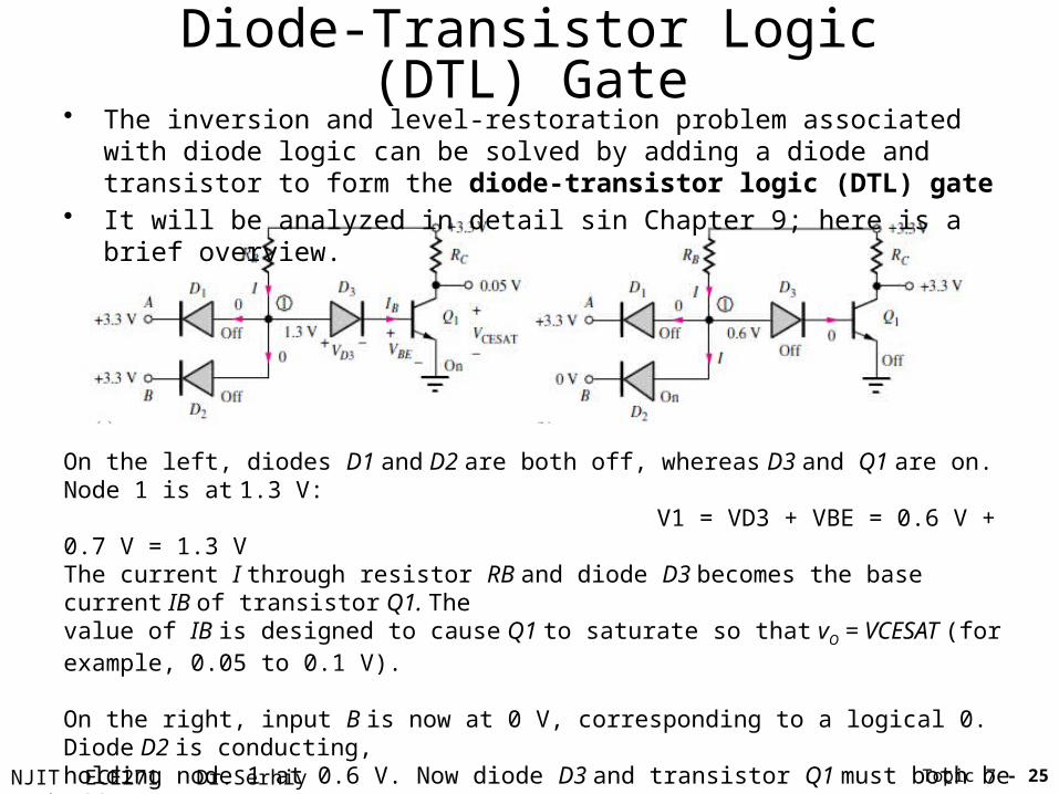
NJIT ECE271 Dr.Serhiy Levkov
Diode-Transistor Logic (DTL) Gate
Topic 7 - 25
On the left, diodes D1 and D2 are both off, whereas D3 and Q1 are on. Node 1 is at 1.3 V: V1 = VD3 + VBE = 0.6 V + 0.7 V = 1.3 VThe current I through resistor RB and diode D3 becomes the base current IB of transistor Q1. Thevalue of IB is designed to cause Q1 to saturate so that vO = VCESAT (for example, 0.05 to 0.1 V).
On the right, input B is now at 0 V, corresponding to a logical 0. Diode D2 is conducting,holding node 1 at 0.6 V. Now diode D3 and transistor Q1 must both be off, because the voltage atnode 1 is now less than the two diode voltage drops required to turn on both D3 and Q1. The basecurrent of Q1 is now zero; Q1 will be off with IC = 0, and the output voltage will be at +3.3 V,corresponding to a logical 1. A similar situation holds for the circuit if both inputs are low.
• The inversion and level-restoration problem associated with diode logic can be solved by adding a diode and transistor to form the diode-transistor logic (DTL) gate
• It will be analyzed in detail sin Chapter 9; here is a brief overview.

NJIT ECE271 Dr.Serhiy Levkov
The Ideal Inverter
The ideal inverter has the following voltage transfer characteristic (VTC) and is described by the following symbol
Topic 7 - 26
?

NJIT ECE271 Dr.Serhiy Levkov
The Ideal Inverter
The ideal inverter has the following voltage transfer characteristic (VTC) and is described by the following symbol
V+ and V- are the supply rails
VH and VL describe the high and low logic levels at the output
Topic 7 - 27

NJIT ECE271 Dr.Serhiy Levkov
Inverter - circuit
An inverter operating with power supplies at V+ and 0 V can be implemented using a switch with a resistive load.
Topic 7 - 28
?MOSFET

NJIT ECE271 Dr.Serhiy Levkov
Inverter - circuit
An inverter operating with power supplies at V+ and 0 V can be implemented using a switch with a resistive load.
Topic 7 - 29
?Q-point

NJIT ECE271 Dr.Serhiy Levkov
Inverter - circuit
An inverter operating with power supplies at V+ and 0 V can be implemented using a switch with a resistive load.
Topic 7 - 30
Q-point

NJIT ECE271 Dr.Serhiy Levkov
Inverter - circuit
An inverter operating with power supplies at V+ and 0 V can be implemented using a switch with a resistive load.
Topic 7 - 31

NJIT ECE271 Dr.Serhiy Levkov
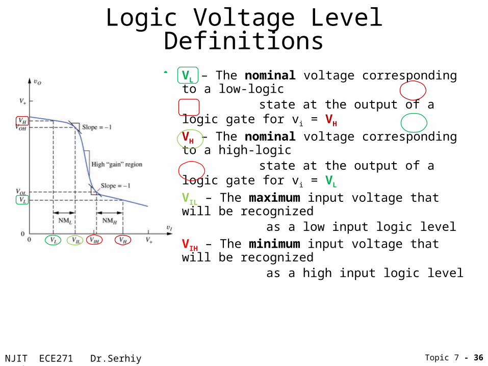
VTC of Non-Ideal Inverter Voltage Level Definitions
For the (VTC) of the non-ideal inverter no Vref is defined. There is now an undefined logic state. The points (VIH ,VOL ) and (VIL ,VOH ) are defined as the points on the VTC curve where slope is -1.
Topic 7 - 32

NJIT ECE271 Dr.Serhiy Levkov
Logic Voltage Level Definitions
• VL – The nominal voltage corresponding to a low-logic
state at the output of a logic gate for vi = VH
Topic 7 - 33
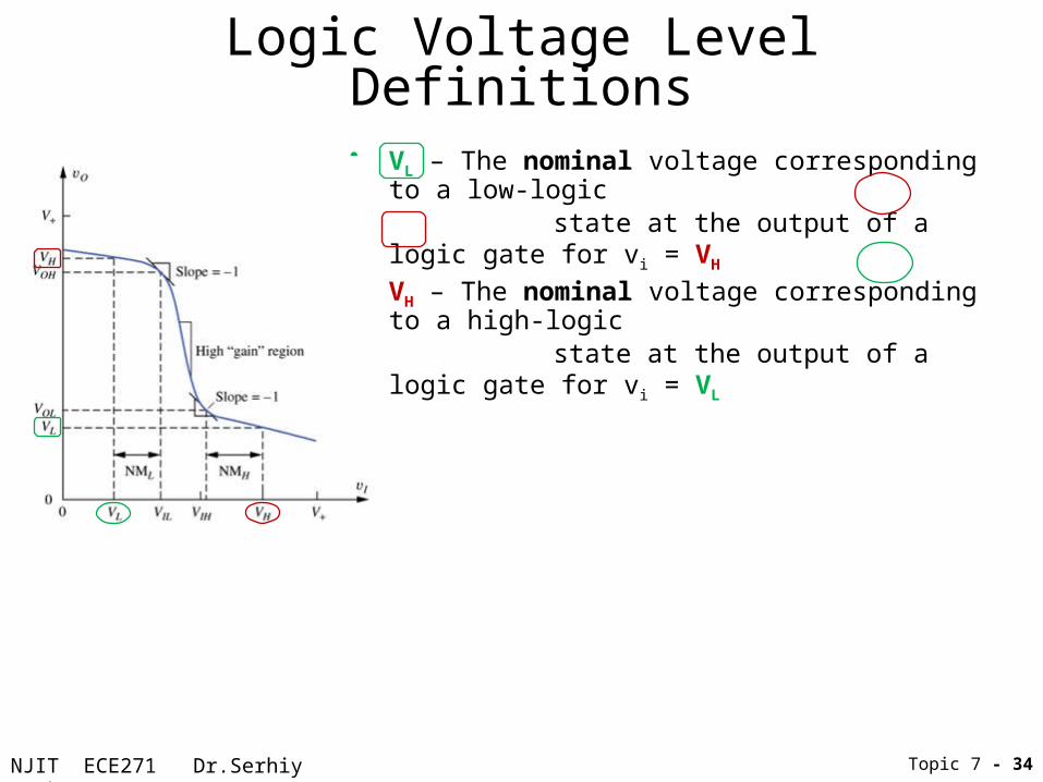
NJIT ECE271 Dr.Serhiy Levkov
Logic Voltage Level Definitions
• VL – The nominal voltage corresponding to a low-logic
state at the output of a logic gate for vi = VH
• VH – The nominal voltage corresponding to a high-logic
state at the output of a logic gate for vi = VL
Topic 7 - 34

NJIT ECE271 Dr.Serhiy Levkov
Logic Voltage Level Definitions
• VL – The nominal voltage corresponding to a low-logic
state at the output of a logic gate for vi = VH
• VH – The nominal voltage corresponding to a high-logic
state at the output of a logic gate for vi = VL
• VIL – The maximum input voltage that will be recognized as a low input logic level
Topic 7 - 35
NJIT ECE271 Dr.Serhiy Levkov
Logic Voltage Level Definitions
• VL – The nominal voltage corresponding to a low-logic
state at the output of a logic gate for vi = VH
• VH – The nominal voltage corresponding to a high-logic
state at the output of a logic gate for vi = VL
• VIL – The maximum input voltage that will be recognized as a low input logic level• VIH – The minimum input voltage that will be recognized as a high input logic level
Topic 7 - 36

NJIT ECE271 Dr.Serhiy Levkov
Logic Voltage Level Definitions
• VL – The nominal voltage corresponding to a low-logic
state at the output of a logic gate for vi = VH
• VH – The nominal voltage corresponding to a high-logic
state at the output of a logic gate for vi = VL
• VIL – The maximum input voltage that will be recognized as a low input logic level• VIH – The minimum input voltage that will be recognized as a high input logic level• VOH – The output voltage corresponding to an input
voltage of VIL
Topic 7 - 37

NJIT ECE271 Dr.Serhiy Levkov
Logic Voltage Level Definitions
• VL – The nominal voltage corresponding to a low-logic
state at the output of a logic gate for vi = VH
• VH – The nominal voltage corresponding to a high-logic
state at the output of a logic gate for vi = VL
• VIL – The maximum input voltage that will be recognized as a low input logic level• VIH – The minimum input voltage that will be recognized as a high input logic level• VOH – The output voltage corresponding to an input
voltage of VIL
• VOL – The output voltage corresponding to an input
voltage of VIH
Topic 7 - 38

NJIT ECE271 Dr.Serhiy Levkov
Logic Voltage Level Definitions
• VL – The nominal voltage corresponding to a low-logic
state at the output of a logic gate for vi = VH
• VH – The nominal voltage corresponding to a high-logic
state at the output of a logic gate for vi = VL
• VIL – The maximum input voltage that will be recognized as a low input logic level• VIH – The minimum input voltage that will be recognized as a high input logic level• VOH – The output voltage corresponding to an input
voltage of VIL
• VOL – The output voltage corresponding to an input
voltage of VIH
Typically, V-=0.
V+=5 for bipolar logic,
V+=1.8, 2.5, 3.3 for MOS logic
V+=1.0-1.5 for ultra low voltage logicTopic 7 - 39
NJIT ECE271 Dr.Serhiy Levkov
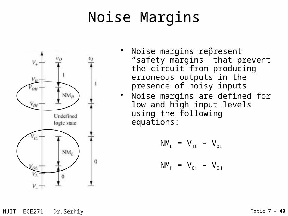
Noise Margins
• Noise margins represent “safety margins” that prevent the circuit from producing erroneous outputs in the presence of noisy inputs
• Noise margins are defined for low and high input levels using the following equations:
NML = VIL – VOL
NMH = VOH – VIH
Topic 7 - 40
NJIT ECE271 Dr.Serhiy Levkov
Logic Gate Design Goals
• An ideal logic gate is highly nonlinear and attempts to quantize the input signal to two discrete states. In an actual gate, the designer should attempt to minimize the undefined input region while maximizing noise margins
Topic 7 - 41

NJIT ECE271 Dr.Serhiy Levkov
Logic Gate Design Goals
• An ideal logic gate is highly nonlinear and attempts to quantize the input signal to two discrete states. In an actual gate, the designer should attempt to minimize the undefined input region while maximizing noise margins
• The logic gate is unidirectional. Changes at the output should have no effect on the input.
Topic 7 - 42

NJIT ECE271 Dr.Serhiy Levkov
Logic Gate Design Goals
• An ideal logic gate is highly nonlinear and attempts to quantize the input signal to two discrete states. In an actual gate, the designer should attempt to minimize the undefined input region while maximizing noise margins
• The logic gate is unidirectional. Changes at the output should have no effect on the input.
• Voltage levels at the output of one gate should be compatible with the input levels of a following gate
Topic 7 - 43
NJIT ECE271 Dr.Serhiy Levkov
Logic Gate Design Goals
• An ideal logic gate is highly nonlinear and attempts to quantize the input signal to two discrete states. In an actual gate, the designer should attempt to minimize the undefined input region while maximizing noise margins
• The logic gate is unidirectional. Changes at the output should have no effect on the input.
• Voltage levels at the output of one gate should be compatible with the input levels of a following gate
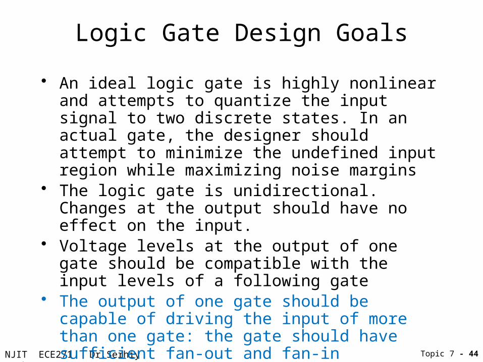
• The output of one gate should be capable of driving the input of more than one gate: the gate should have sufficient fan-out and fan-in capabilities
Topic 7 - 44

NJIT ECE271 Dr.Serhiy Levkov
Logic Gate Design Goals
• An ideal logic gate is highly nonlinear and attempts to quantize the input signal to two discrete states. In an actual gate, the designer should attempt to minimize the undefined input region while maximizing noise margins
• The logic gate is unidirectional. Changes at the output should have no effect on the input.
• Voltage levels at the output of one gate should be compatible with the input levels of a following gate
• The output of one gate should be capable of driving the input of more than one gate: the gate should have sufficient fan-out and fan-in capabilities
• The gate should consume minimal power (and area for ICs) and still operate under the design specifications
Topic 7 - 45

NJIT ECE271 Dr.Serhiy Levkov
Dynamic Response of Logic Gates
Topic 7 - 46
• An important characteristic of the logical gates is the response in the time domain
• To describe the typical pulse signal at the input, we introduce:
The rise and fall times: tf and tr, are measured at the 10% and 90% points on the transitions between the two states as shown by the following expressions:
V10% = VL + 0.1V
V90% = VL + 0.9V = VH – 0.1V
where V is the logic swing given by V = VH - VL
•

NJIT ECE271 Dr.Serhiy Levkov
Dynamic Response of Logic Gates
Topic 7 - 47
• For the input on the top, will the output will be like the signal on the bottom plot?

NJIT ECE271 Dr.Serhiy Levkov
Dynamic Response of Logic Gates
Topic 7 - 48
• For the input on the top, will the output will be like the signal on the bottom plot?
• No, It will be delayed.

NJIT ECE271 Dr.Serhiy Levkov
Dynamic Response of Logic Gates
Topic 7 - 49
• For the input on the top, will the output will be like the signal on the bottom plot?
• No, It will be delayed.• Propagation delay describes the
amount of time between the input reaching the 50% point and the output reaching the 50% point. The 50% point is described by the following:
• The high-to-low propagation delay, PHL, and the low-to-high propagation delay, PLH, are usually not equal, but can be combined as an average value:
V50% VH VL
2
2PHL P
PLH
PHL

NJIT ECE271 Dr.Serhiy Levkov
NMOS Logic Design
• MOS transistors (both PMOS and NMOS) can be combined with resistive loads to create single channel logic gates.
Topic 7 - 50

NJIT ECE271 Dr.Serhiy Levkov
NMOS Logic Design
• MOS transistors (both PMOS and NMOS) can be combined with resistive loads to create single channel logic gates.
• In most logic design situations, the power supply voltage is predetermined by either technology reliability constraints or system-level criteria
• The circuit designer is limited to altering circuit topology and the width-to-length (W/L) ratio since the other factors are dependent upon processing parameters
Topic 7 - 51
NJIT ECE271 Dr.Serhiy Levkov
NMOS Logic Design
• MOS transistors (both PMOS and NMOS) can be combined with resistive loads to create single channel logic gates.
• In most logic design situations, the power supply voltage is predetermined by either technology reliability constraints or system-level criteria
• The circuit designer is limited to altering circuit topology and the width-to-length (W/L) ratio since the other factors are dependent upon processing parameters
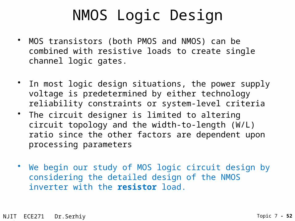
• We begin our study of MOS logic circuit design by considering the detailed design of the NMOS inverter with the resistor load.
Topic 7 - 52

NJIT ECE271 Dr.Serhiy Levkov
NMOS Logic Design
• MOS transistors (both PMOS and NMOS) can be combined with resistive loads to create single channel logic gates.
• In most logic design situations, the power supply voltage is predetermined by either technology reliability constraints or system-level criteria
• The circuit designer is limited to altering circuit topology and the width-to-length (W/L) ratio since the other factors are dependent upon processing parameters
• We begin our study of MOS logic circuit design by considering the detailed design of the NMOS inverter with the resistor load.
• In integrated logic circuits, the load resistor occupies too much silicon area, and is replaced by a second NMOS transistor. This “load device” can be connected in three different configurations called the saturated load, linear load, and depletion-mode load circuits.
Topic 7 - 53

NJIT ECE271 Dr.Serhiy Levkov
NMOS Inverter with a Resistive Load
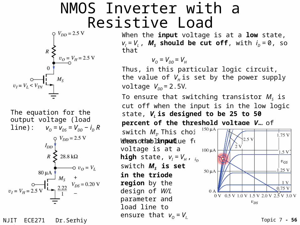
• The basic inverter circuit consists of an NMOS switching device MS and a resistor load element.
• MS is the switching transistor used to “pull” the output high - toward to the power supply VDD
• The resistor R is used to “pull” the output low, to force vO to VL
• The size of R and the W/L ratio of MS are the design factors that need to be chosen.
Topic 7 - 54

NJIT ECE271 Dr.Serhiy Levkov
NMOS Inverter with a Resistive LoadWhen the input voltage is at a low state, vI = VL , MS should be cut off, with iD = 0, so that
vO = VDD = VH
Thus, in this particular logic circuit, the value of VH is set by the power supply voltage VDD = 2.5V.
To ensure that switching transistor MS is cut off when the input is in the low logic state, VL is designed to be 25 to 50 percent of the threshold voltage VTN of switch MS. This choice also provides a reasonable value for noise margin NML .
Topic 7 - 55
The equation for the output voltage (load line): vO = vDS = VDD − iD R
NJIT ECE271 Dr.Serhiy Levkov
NMOS Inverter with a Resistive LoadWhen the input voltage is at a low state, vI = VL , MS should be cut off, with iD = 0, so that
vO = VDD = VH
Thus, in this particular logic circuit, the value of VH is set by the power supply voltage VDD = 2.5V.
To ensure that switching transistor MS is cut off when the input is in the low logic state, VL is designed to be 25 to 50 percent of the threshold voltage VTN of switch MS. This choice also provides a reasonable value for noise margin NML .
Topic 7 - 56
When the input voltage is at a high state, vI = VH , switch MS is set in the triode region by the design of W/L parameter and load line to ensure that vO = VL.
The equation for the output voltage (load line): vO = vDS = VDD − iD R

NJIT ECE271 Dr.Serhiy Levkov
NMOS with Resistive LoadDesign Example (1)
• Design a NMOS resistive load inverter for – VDD = 3.3 V
– P = 0.1 mW when VL = 0.2 V
– Kn = 60 A/V2
– VTN = 0.75 V
Topic 7 - 57
• Find the value of the load resistor R and the W/L ratio of the switching transistor MS
ov
DDI
NJIT ECE271 Dr.Serhiy Levkov
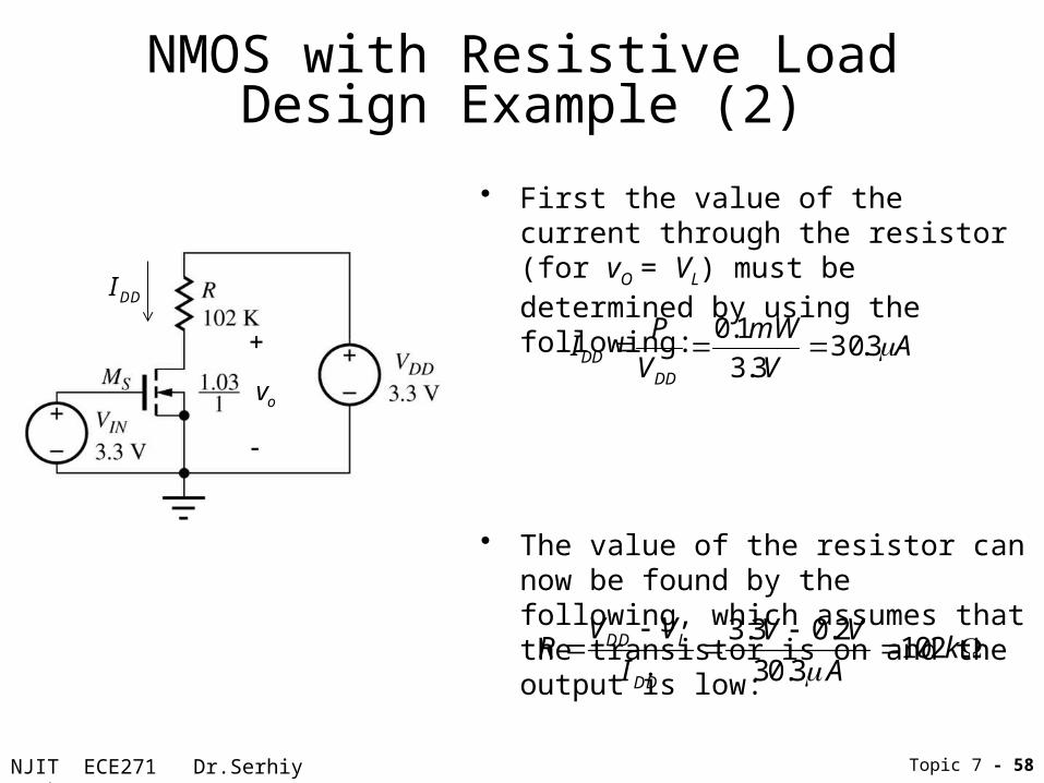
• First the value of the current through the resistor (for vO = VL) must be determined by using the following:
• The value of the resistor can now be found by the following, which assumes that the transistor is on and the output is low:
IDD P
VDD
0.1mW
3.3V30.3A
3.3 0.2102
30.3DD L
DD
V V V VR k
I A
Topic 7 - 58
NMOS with Resistive LoadDesign Example (2)
ov
DDI

NJIT ECE271 Dr.Serhiy Levkov
• For vI = VH = 3.3 V, and vO = VL = 0.2V, the transistor’s drain-source voltage VDS =VL will be less than VGS -VTN=VH -VTN
• Therefore it will be operating in the triode region. Using the triode region equation for the MOSFET, the W/L ratio can be found:
ID Kn' W
L
S
VH VTN VL
2
VL
30.3A 6010 6 W
L
S
3.3 0.75 0.2
2
0.2
W
L
S
1.03
11
1
Topic 7 - 59
NMOS with Resistive LoadDesign Example (3)
ov
DDI
NJIT ECE271 Dr.Serhiy Levkov
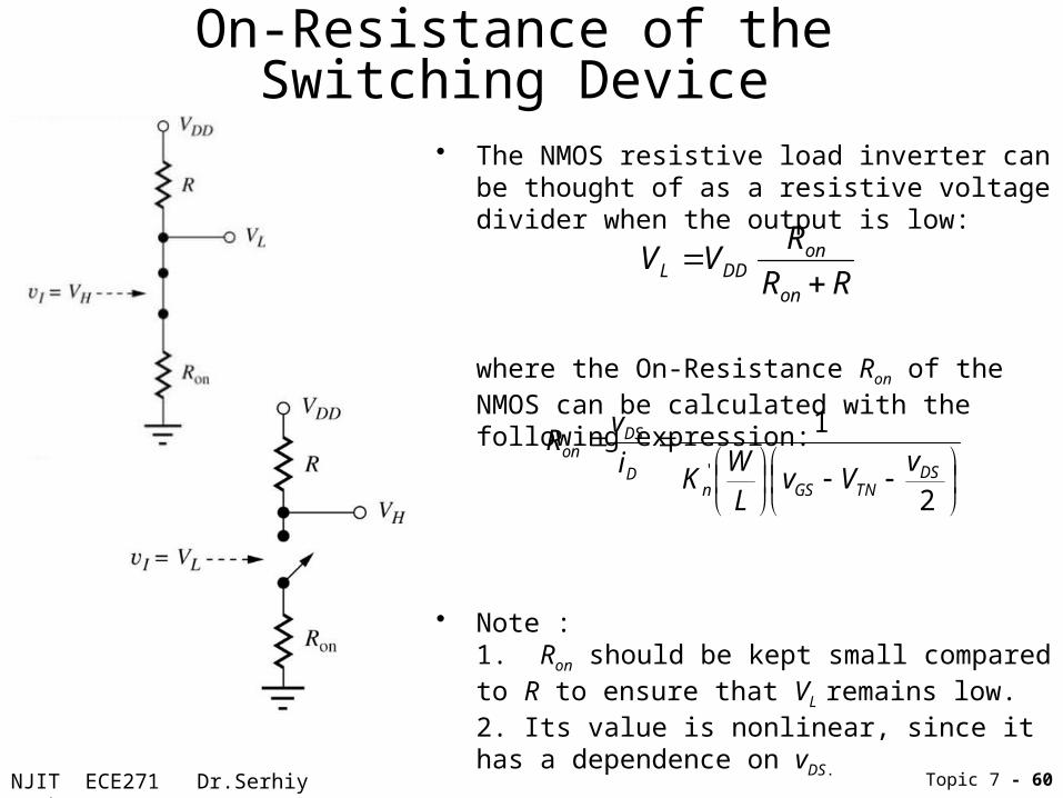
On-Resistance of the Switching Device
• The NMOS resistive load inverter can be thought of as a resistive voltage divider when the output is low:
where the On-Resistance Ron of the NMOS can be calculated with the following expression:
• Note : 1. Ron should be kept small compared to R to ensure that VL remains low. 2. Its value is nonlinear, since it has a dependence on vDS.
RR
RVV
on
onDDL
Topic 7 - 60
2
1
' DSTNGSn
D
DSon v
VvL
WK
i
vR

NJIT ECE271 Dr.Serhiy Levkov Topic 7 - 61
Noise Margin Analysis
The following equations (base on the calculation of the derivatives of vO =VDD –iDR with respect to vI ) can be used to determine the various parameters needed to determine the noise margin of NMOS resistive load inverters
RK
VV
RK
V
RKVV
RKVV
RKVV
n
DDOL
n
DD
nTNIH
nDDOH
nTNIL
3
2
63.11
2
1
1

NJIT ECE271 Dr.Serhiy Levkov
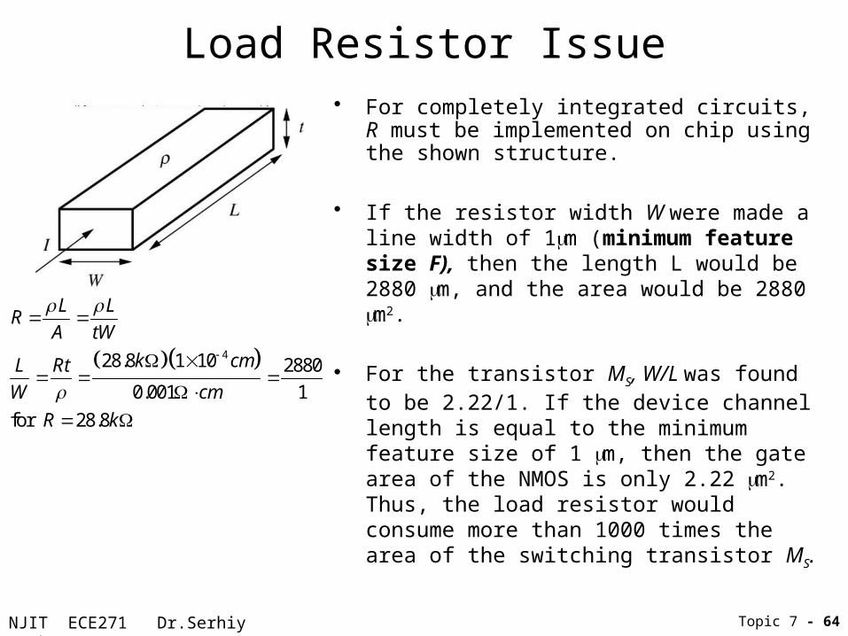
Load Resistor Issue• For completely integrated circuits, R must be
implemented on chip using the shown structure.
428.8 1 10 2880
0.001 1
for 28.8
L LR
A tW
k cmL Rt
W cm
R k
Topic 7 - 62

NJIT ECE271 Dr.Serhiy Levkov
Load Resistor Issue• For completely integrated circuits, R must be
implemented on chip using the shown structure.
• If the resistor width W were made a line width of 1mm (minimum feature size F), then the length L would be 2880 mm, and the area would be 2880 mm2.
Topic 7 - 63
428.8 1 10 2880
0.001 1
for 28.8
L LR
A tW
k cmL Rt
W cm
R k
NJIT ECE271 Dr.Serhiy Levkov
Load Resistor Issue• For completely integrated circuits, R must be
implemented on chip using the shown structure.
• If the resistor width W were made a line width of 1mm (minimum feature size F), then the length L would be 2880 mm, and the area would be 2880 mm2.
• For the transistor MS, W/L was found to be 2.22/1. If the device channel length is equal to the minimum feature size of 1 mm, then the gate area of the NMOS is only 2.22 mm2. Thus, the load resistor would consume more than 1000 times the area of the switching transistor MS.
Topic 7 - 64
428.8 1 10 2880
0.001 1
for 28.8
L LR
A tW
k cmL Rt
W cm
R k

NJIT ECE271 Dr.Serhiy Levkov
Load Resistor Issue• For completely integrated circuits, R must be
implemented on chip using the shown structure.
• If the resistor width W were made a line width of 1mm (minimum feature size F), then the length L would be 2880 mm, and the area would be 2880 mm2.
• For the transistor MS, W/L was found to be 2.22/1. If the device channel length is equal to the minimum feature size of 1 mm, then the gate area of the NMOS is only 2.22 mm2. Thus, the load resistor would consume more than 1000 times the area of the switching transistor MS.
• This is simply not an acceptable utilization of area in IC design.
Topic 7 - 65
428.8 1 10 2880
0.001 1
for 28.8
L LR
A tW
k cmL Rt
W cm
R k

NJIT ECE271 Dr.Serhiy Levkov
Load Resistor Issue• For completely integrated circuits, R must be
implemented on chip using the shown structure.
• If the resistor width W were made a line width of 1mm (minimum feature size F), then the length L would be 2880 mm, and the area would be 2880 mm2.
• For the transistor MS, W/L was found to be 2.22/1. If the device channel length is equal to the minimum feature size of 1 mm, then the gate area of the NMOS is only 2.22 mm2. Thus, the load resistor would consume more than 1000 times the area of the switching transistor MS.
• This is simply not an acceptable utilization of area in IC design.
• The solution to this problem is to replace the load resistor with a transistor. Topic 7 - 66
428.8 1 10 2880
0.001 1
for 28.8
L LR
A tW
k cmL Rt
W cm
R k

NJIT ECE271 Dr.Serhiy Levkov
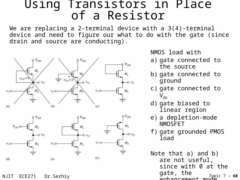
Using Transistors in Place of a Resistor
NMOS load transistor with a) gate connected to the sourceb) gate connected to ground
c) gate connected to VDD
d) gate biased to linear regione) a depletion-mode NMOSFETf) gate grounded PMOS load
Topic 7 - 67
We are replacing a 2-terminal device with a 3(4)-terminal device and need to figure our what to do with the gate (since drain and source are conducting).
NJIT ECE271 Dr.Serhiy Levkov
Using Transistors in Place of a Resistor
NMOS load with a) gate connected to the sourceb) gate connected to ground
c) gate connected to VDD
d) gate biased to linear regione) a depletion-mode NMOSFETf) gate grounded PMOS load
Note that a) and b) are not useful, since with 0 at the gate, the enhancement mode NMOS is not conducting.
We’ll consider other methods starting from (c)
Topic 7 - 68
We are replacing a 2-terminal device with a 3(4)-terminal device and need to figure our what to do with the gate (since drain and source are conducting).

NJIT ECE271 Dr.Serhiy Levkov
NMOS Saturated Load Inverter
Schematic for a NMOSsaturated load inverter
The substrate is common and grounded:
Topic 7 - 69
It’s the (c) on diagram, called saturated because ML is in saturation region: vDS = vGS vDS ≥ vGS − VTN for VTN ≥ 0

NJIT ECE271 Dr.Serhiy Levkov
NMOS Saturated Load Inverter
Schematic for a NMOSsaturated load inverter
The substrate is common and grounded:
vSB=0 for MS .
Topic 7 - 70
It’s the (c) on diagram, called saturated because ML is in saturation region: vDS = vGS vDS ≥ vGS − VTN for VTN ≥ 0

NJIT ECE271 Dr.Serhiy Levkov
NMOS Saturated Load Inverter
Schematic for a NMOSsaturated load inverter
The substrate is common and grounded:
vSB=0 for MS .
vSB=vO for ML ,
Topic 7 - 71
It’s the (c) on diagram, called saturated because ML is in saturation region: vDS = vGS vDS ≥ vGS − VTN for VTN ≥ 0

NJIT ECE271 Dr.Serhiy Levkov
NMOS Saturated Load Inverter
Schematic for a NMOSsaturated load inverter
The substrate is common and grounded:
vSB=0 for MS .
vSB=vO for ML ,
thus VTN is generally different for both.
Topic 7 - 72
It’s the (c) on diagram, called saturated because ML is in saturation region: vDS = vGS vDS ≥ vGS − VTN for VTN ≥ 0

NJIT ECE271 Dr.Serhiy Levkov
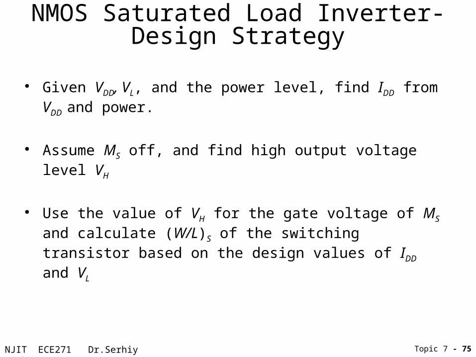
NMOS Saturated Load Inverter-Design Strategy
• Given VDD, VL, and the power level, find IDD from VDD and power.
Topic 7 - 73

NJIT ECE271 Dr.Serhiy Levkov
NMOS Saturated Load Inverter-Design Strategy
• Given VDD, VL, and the power level, find IDD from VDD and power.
• Assume MS off, and find high output voltage level VH
Topic 7 - 74
NJIT ECE271 Dr.Serhiy Levkov
NMOS Saturated Load Inverter-Design Strategy
• Given VDD, VL, and the power level, find IDD from VDD and power.
• Assume MS off, and find high output voltage level VH
• Use the value of VH for the gate voltage of MS and calculate (W/L)S of the switching transistor based on the design values of IDD and VL
Topic 7 - 75

NJIT ECE271 Dr.Serhiy Levkov
NMOS Saturated Load Inverter-Design Strategy
• Given VDD, VL, and the power level, find IDD from VDD and power.
• Assume MS off, and find high output voltage level VH
• Use the value of VH for the gate voltage of MS and calculate (W/L)S of the switching transistor based on the design values of IDD and VL
• Use the value of VH for the gate voltage of MS and find (W/L)L of the load transistor based on IDD and VL
Topic 7 - 76

NJIT ECE271 Dr.Serhiy Levkov
NMOS Saturated Load Inverter-Design Strategy
• Given VDD, VL, and the power level, find IDD from VDD and power.
• Assume MS off, and find high output voltage level VH
• Use the value of VH for the gate voltage of MS and calculate (W/L)S of the switching transistor based on the design values of IDD and VL
• Use the value of VH for the gate voltage of MS and find (W/L)L of the load transistor based on IDD and VL
• Check the operating region assumptions of MS and ML for vo = VL
Topic 7 - 77

NJIT ECE271 Dr.Serhiy Levkov
NMOS Saturated Load Inverter - Example
3.3
0.2
0.2
DD
L
V V
V V
P mW
Kn' 50A /V 2
VTO 0.75V
0.5 V
2F 0.6V
Topic 7 - 78
Design an saturated load inverter given the following specifications:
VVDD 3.3
DDI

NJIT ECE271 Dr.Serhiy Levkov
NMOS Saturated Load Inverter - Example• First, set vi = VH ,vO = VL, MS - on, and find the
value of the current through the resistor using the power :
3.3
0.2
0.2
DD
L
V V
V V
P mW
Kn' 50A /V 2
VTO 0.75V
0.5 V
2F 0.6V
Topic 7 - 79
Design an saturated load inverter given the following specifications:
VVDD 3.3
DDI
0.260
3.3DDDD
P mWI A
V V
LIN
SAT
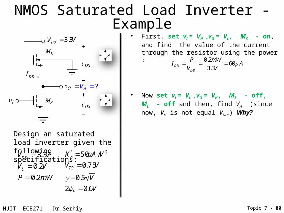
NJIT ECE271 Dr.Serhiy Levkov
NMOS Saturated Load Inverter - Example• First, set vi = VH ,vO = VL, MS - on, and find the
value of the current through the resistor using the power :
• Now set vi = VL ,vO = VH, MS - off, ML - off and then, find VH (since now, VH is not equal VDD.) Why?
3.3
0.2
0.2
DD
L
V V
V V
P mW
Kn' 50A /V 2
VTO 0.75V
0.5 V
2F 0.6V
Topic 7 - 80
0.260
3.3DDDD
P mWI A
V V
Design an saturated load inverter given the following specifications:
VVDD 3.3
DDI
?HV

NJIT ECE271 Dr.Serhiy Levkov
NMOS Saturated Load Inverter - Example• First, set vi = VH ,vO = VL, MS - on, and find the value
of the current through the resistor using the power :
• Now set vi = VL ,vO = VH, MS - off, ML - off and then, find VH (since now, VH is not equal VDD.) Why?
• When MS turns off from the on state, the current IDD will stop when the value of vGSL will reach VTNL, (vGS > VTN, for IDD to exist)
vGSL = VDD − vO = VTN VH = VDD − VTN .
Thus, taking into account the body effect (g) and surface potential parameter (fF):
(The output cannot exceed the positive power supply voltage.)
3.3
0.2
0.2
DD
L
V V
V V
P mW
Kn' 50A /V 2
VTO 0.75V
0.5 V
2F 0.6V
Topic 7 - 81
Design an saturated load inverter given the following specifications:
2 2
3.3 0.75 0.5
4.
0.6 0.6
, ,since 1 02.1 1
H DD TNL DD TO SB F F
H H
H H DD
V V V V V V
V V
V V V V V
VVDD 3.3
DDI
2.11HV V
0.260
3.3DDDD
P mWI A
V V
HV
HV

NJIT ECE271 Dr.Serhiy Levkov
'
6
2
0.260 50 10 2.11 0.75 0.2
2
4.76
1
DSDS n GS TN DS
S
S
S
VWI K V V V
L
WA
L
W
L
Topic 7 - 82
NMOS Saturated Load Inverter - Example
'2
26
,2
0.75 0.5 0.2 0.6 0.6 0.81
60 50 10 3.3 0.2 0.81
1
2.19
nDL GSL TNL GSL
L
TNL
L
L
DD LV VK W
I V V VL
V V
WA
L
W
L
• Now we can find W/L for both transistors MS and then ML.
• Set vi = VH , vo = VL: MS is in the triode region (on) ML is in saturation (on).
DLI
DSI
Check the operating region. For the switch, VGS − VTN = 2.11 − 0.75 = 1.36 V, which is greater than VDS = 0.2 V, and the triode region assumption is correct. For the load device, VGS − VTN =3.1 − 0.81 = 2.29 V and is less than VDS = 3.1 V, which is consistent with the saturation region of operation.
HV LV
LIN
SAT

NJIT ECE271 Dr.Serhiy Levkov Topic 7 - 83
NMOS Saturated Load Inverter -Noise Margin
From the PSPICE simulation typical noise margins are:
NMH = VOH - VIH = 1.55 - 1.42 = 0.33 V
NML = VIL - VOL = 0.90 - 0.38 = 0.22 V
The detailed analysis of the noise margins for saturated load inverter is quite tedious. Instead, the PSPICE simulation can be used. Example:

NJIT ECE271 Dr.Serhiy Levkov
NMOS Inverter with a Linear Load
• This inverter has a load transistor that is biased with VGG defined by the following:
DDG TNG LV V V
Topic 7 - 84

NJIT ECE271 Dr.Serhiy Levkov
• This inverter has a load transistor that is biased with VGG defined by the following:
• This causes the load transistor to operate in the linear region:
vGSL − VTNL = VGG − vo − VTNL
Topic 7 - 85
NMOS Inverter with a Linear Load
DDG TNG LV V V

NJIT ECE271 Dr.Serhiy Levkov
• This inverter has a load transistor that is biased with VGG defined by the following:
• This causes the load transistor to operate in the linear region:
vGSL − VTNL = VGG − vo − VTNL
≥ VDD + VTNL − vo − VTNL
≥ VDD − vo = vDSL
• For this value of VGG, the output voltage in the high output state VH is equal to VDD:
MS -off, iD=0 vDSL=0 (linear region) vDSL= VDD − vo = VDD − VH =0 VH = VDD
GG DD TNLV V V
Topic 7 - 86
NMOS Inverter with a Linear Load

NJIT ECE271 Dr.Serhiy Levkov
• This inverter has a load transistor that is biased with VGG defined by the following:
• This causes the load transistor to operate in the linear region:
vGSL − VTNL = VGG − vo − VTNL
≥ VDD + VTNL − vo − VTNL
≥ VDD − vo = vDSL
• For this value of VGG, the output voltage in the high output state VH is equal to VDD:
MS -off, iD=0 vDSL=0 (linear region) vDSL= VDD − vo = VDD − VH =0 VH = VDD
• The W/L ratios for MS and ML can be calculated as in previous section ( easier, since VH is equal to VDD) Topic 7 - 87
NMOS Inverter with a Linear Load
GG DD TNLV V V

NJIT ECE271 Dr.Serhiy Levkov
NMOS Inverter with a Depletion-mode Load
Topic 7 - 88
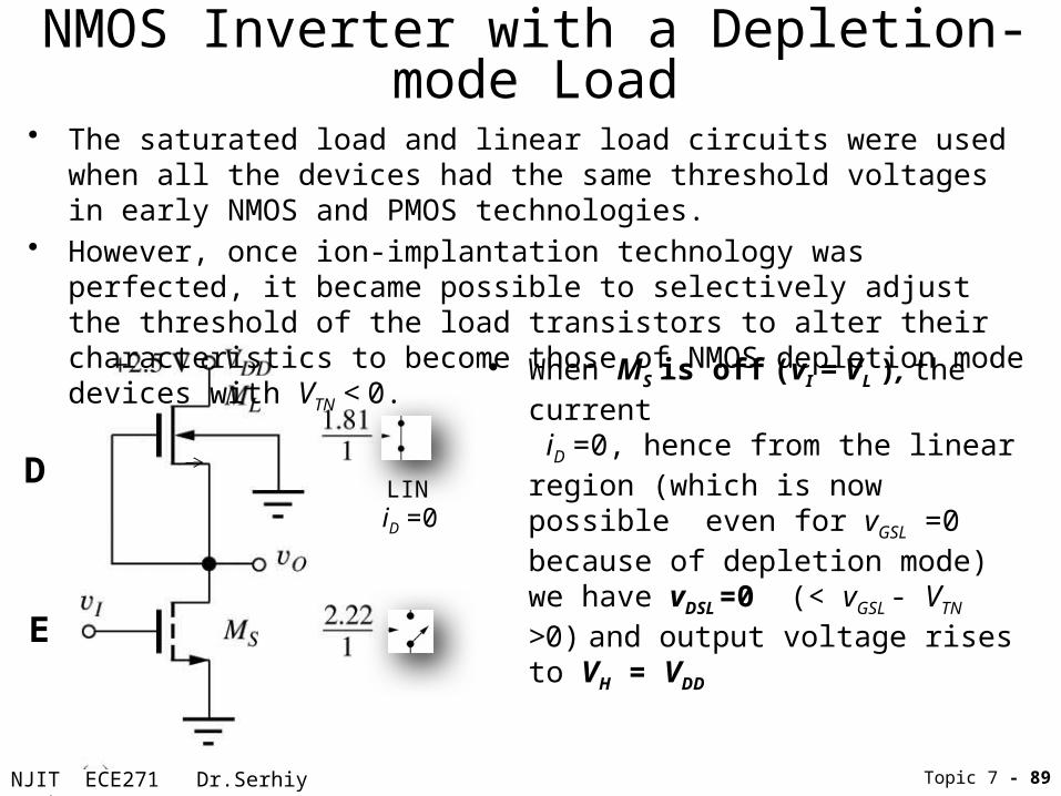
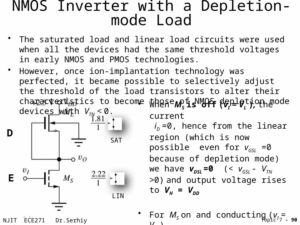
• The saturated load and linear load circuits were used when all the devices had the same threshold voltages in early NMOS and PMOS technologies.
• However, once ion-implantation technology was perfected, it became possible to selectively adjust the threshold of the load transistors to alter their characteristics to become those of NMOS depletion mode devices with VTN < 0.
D
E
NJIT ECE271 Dr.Serhiy Levkov
NMOS Inverter with a Depletion-mode Load
• When MS is off (vI = VL ), the current iD =0, hence from the linear region (which is now possible even for vGSL =0 because of depletion mode) we have vDSL =0 (< vGSL - VTN >0) and output voltage rises to VH = VDD
Topic 7 - 89
• The saturated load and linear load circuits were used when all the devices had the same threshold voltages in early NMOS and PMOS technologies.
• However, once ion-implantation technology was perfected, it became possible to selectively adjust the threshold of the load transistors to alter their characteristics to become those of NMOS depletion mode devices with VTN < 0.
D
E
LINiD =0
NJIT ECE271 Dr.Serhiy Levkov
NMOS Inverter with a Depletion-mode Load
• When MS is off (vI = VL ), the current iD =0, hence from the linear region (which is now possible even for vGSL =0 because of depletion mode) we have vDSL =0 (< vGSL - VTN >0) and output voltage rises to VH = VDD
• For MS on and conducting (vI = VH ), vO = VL, ML is designed to be saturated (vDSL = 2.5 - vO > vGSL - VTN ) and MS , as usual, in the triode region.
Topic 7 - 90
• The saturated load and linear load circuits were used when all the devices had the same threshold voltages in early NMOS and PMOS technologies.
• However, once ion-implantation technology was perfected, it became possible to selectively adjust the threshold of the load transistors to alter their characteristics to become those of NMOS depletion mode devices with VTN < 0.
D
E
LIN
SAT

NJIT ECE271 Dr.Serhiy Levkov
• Then we set input to VH a(both transistors on) and find W/L
• To find (W/L)L given iDL (which we find from power requirements) we use the saturation mode for ML with vGS =0 :
• To find (W/L)S where VH = VDD, use the same technique as used for the resistor load inverter:
iDL Kn
'
2
W
L
L
VTNL 2
iDS Kn' W
L
S
VH VTNS VL
2
VL
Topic 7 - 91
DS DLi i
NMOS Inverter with a Depletion-mode Load
NJIT ECE271 Dr.Serhiy Levkov
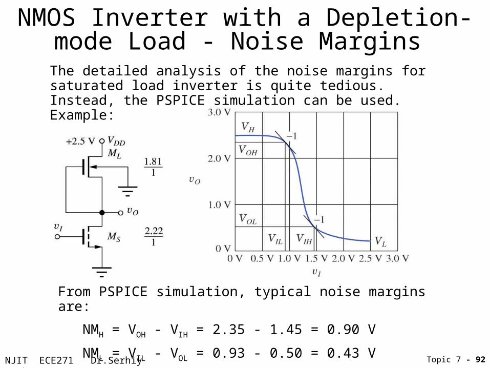
NMOS Inverter with a Depletion-mode Load - Noise Margins
From PSPICE simulation, typical noise margins are:
NMH = VOH - VIH = 2.35 - 1.45 = 0.90 V
NML = VIL - VOL = 0.93 - 0.50 = 0.43 V
Topic 7 - 92
The detailed analysis of the noise margins for saturated load inverter is quite tedious. Instead, the PSPICE simulation can be used. Example:

NJIT ECE271 Dr.Serhiy Levkov
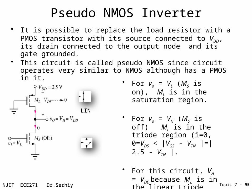
Pseudo NMOS Inverter
Topic 7 - 93
• It is possible to replace the load resistor with a PMOS transistor with its source connected to VDD, its drain connected to the output node and its gate grounded.
• This circuit is called pseudo NMOS since circuit operates very similar to NMOS although has a PMOS in it.
LIN
SAT
• For vo = VL (MS is on), ML is in the saturation region.

NJIT ECE271 Dr.Serhiy Levkov
Pseudo NMOS Inverter
• For vo = VL (MS is on), ML is in the saturation region.
• For vo = VH (MS is off) ML is in the triode region (i=0, 0=VDS < |VGS - VTN |=|2.5 - VTN |.
• For this circuit, VH = VDD
because ML is in the linear triode region and VDS =0 when MS is off.
Topic 7 - 94
• It is possible to replace the load resistor with a PMOS transistor with its source connected to VDD, its drain connected to the output node and its gate grounded.
• This circuit is called pseudo NMOS since circuit operates very similar to NMOS although has a PMOS in it.
LIN
NJIT ECE271 Dr.Serhiy Levkov
Pseudo NMOS Inverter
Topic 7 - 95
• It is possible to replace the load resistor with a PMOS transistor with its source connected to VDD, its drain connected to the output node and its gate grounded.
• This circuit is called pseudo NMOS since circuit operates very similar to NMOS although has a PMOS in it.
LIN
• For vo = VL (MS is on), ML is in the saturation region.
• For vo = VH (MS is off) ML is in the triode region (i=0, 0=VDS < |VGS - VTN |=|2.5 - VTN |.
• For this circuit, VH = VDD
because ML is in the linear triode region and VDS =0 when MS is off.

NJIT ECE271 Dr.Serhiy Levkov
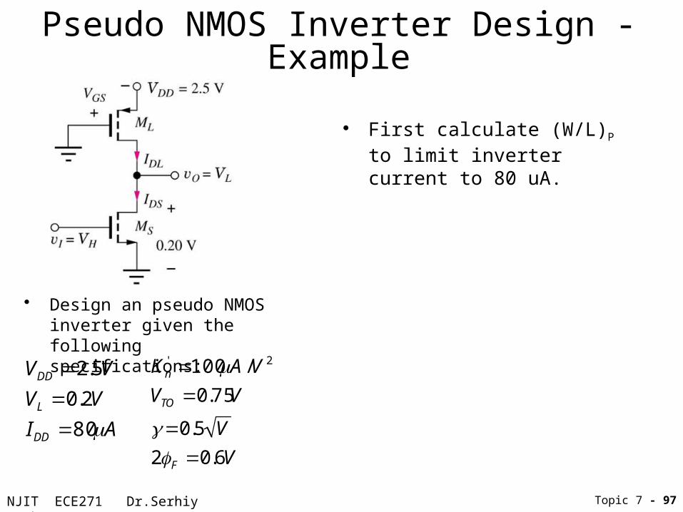
Pseudo NMOS Inverter Design - Example
• Design an pseudo NMOS inverter given the following specifications:
VDD 2.5V
VL 0.2V
IDD 80A
Kn' 100A /V 2
VTO 0.75V
0.5 V
2F 0.6V
Topic 7 - 96
NJIT ECE271 Dr.Serhiy Levkov
Pseudo NMOS Inverter Design - Example
• Design an pseudo NMOS inverter given the following specifications:
VDD 2.5V
VL 0.2V
IDD 80A
Kn' 100A /V 2
VTO 0.75V
0.5 V
2F 0.6V
Topic 7 - 97
• First calculate (W/L)P to limit inverter current to 80 uA.

NJIT ECE271 Dr.Serhiy Levkov
Pseudo NMOS Inverter Design - Example
• Design an pseudo NMOS inverter given the following specifications:
VDD 2.5V
VL 0.2V
IDD 80A
' 2
' 2
100 /
40 /
0.6
0
n
p
TO
K A V
K A V
V V
Topic 7 - 98
'2
2 22
2
4080 2.5 ( 0.6)
2
1.11
1
GS DD
pD GS TP
P
P
P
V V
K WI V V
L
A WA V
LV
W
L
• First calculate (W/L)P to limit inverter current to 80 uA.
MS is on, ML is in saturation:
LIN
SAT
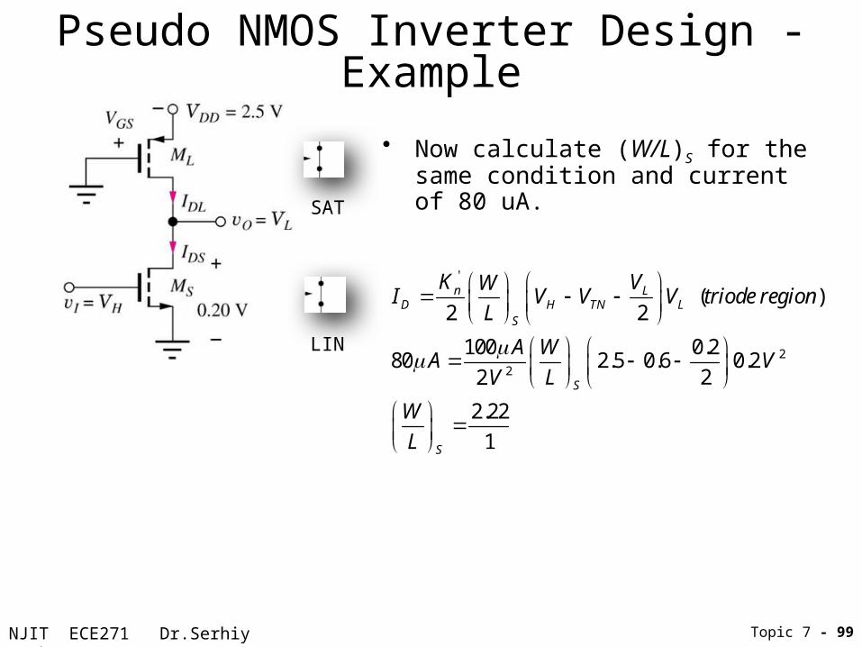
NJIT ECE271 Dr.Serhiy Levkov
Pseudo NMOS Inverter Design - Example
• Now calculate (W/L)S for the same condition and current of 80 uA.
'
22
( )2 2
100 0.280 2.5 0.6 0.2
22
2.22
1
n LD H TN L
S
S
S
K VWI V V V triode region
L
A WA V
LV
W
L
Topic 7 - 99
LIN
SAT
NJIT ECE271 Dr.Serhiy Levkov
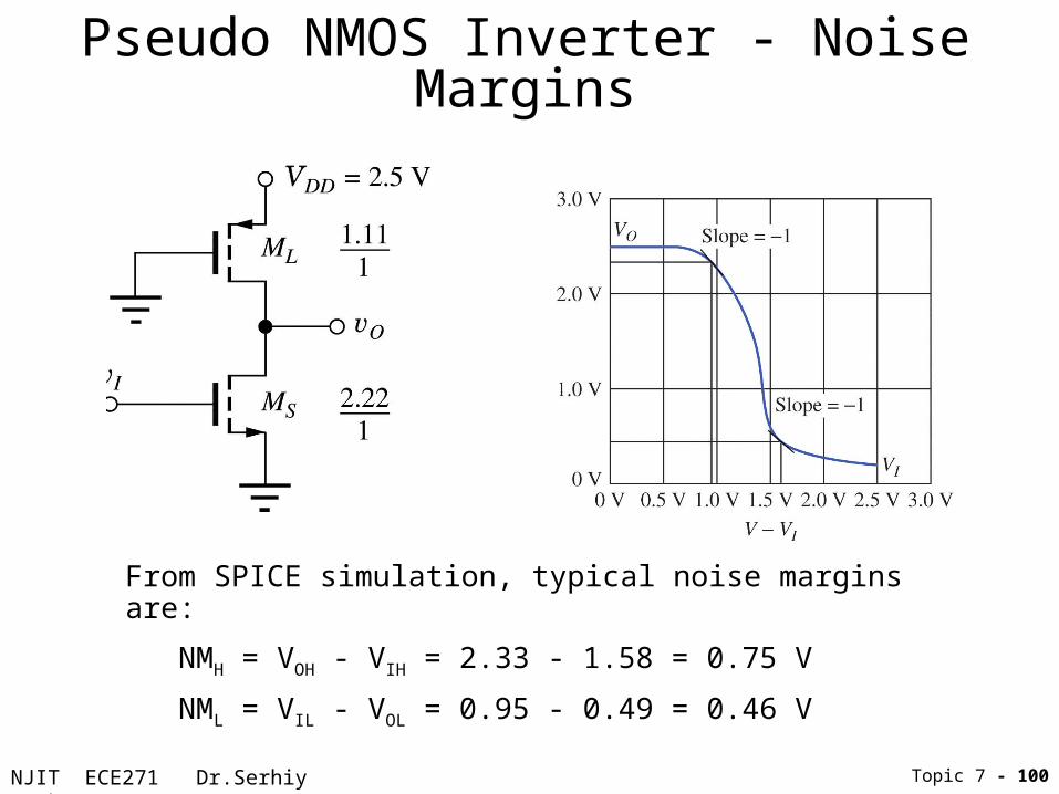
Pseudo NMOS Inverter - Noise Margins
From SPICE simulation, typical noise margins are:
NMH = VOH - VIH = 2.33 - 1.58 = 0.75 V
NML = VIL - VOL = 0.95 - 0.49 = 0.46 V
Topic 7 - 100

NJIT ECE271 Dr.Serhiy Levkov
NMOS Inverter Summary• Resistive load inverter takes up too much area for and IC design.
Topic 7 - 101

NJIT ECE271 Dr.Serhiy Levkov
NMOS Inverter Summary• Resistive load inverter takes up too much area for and IC design.
• The saturated load configuration is the simplest design, but VH never reaches VDD, and it has a slow switching speed.
Topic 7 - 102

NJIT ECE271 Dr.Serhiy Levkov
NMOS Inverter Summary• Resistive load inverter takes up too much area for and IC design.
• The saturated load configuration is the simplest design, but VH never reaches VDD, and it has a slow switching speed.
• The linear load inverter fixes the speed and logic level issues, but it requires an additional power supply for the load gate.
Topic 7 - 103

NJIT ECE271 Dr.Serhiy Levkov
NMOS Inverter Summary• Resistive load inverter takes up too much area for and IC design.
• The saturated load configuration is the simplest design, but VH never reaches VDD, and it has a slow switching speed.
• The linear load inverter fixes the speed and logic level issues, but it requires an additional power supply for the load gate.
• The depletion-mode NMOS load requires the most processing steps, but needs small area to achieve the high speed, VH = VDD, and best combination of noise margins.
Topic 7 - 104

NJIT ECE271 Dr.Serhiy Levkov
NMOS Inverter Summary• Resistive load inverter takes up too much area for and IC design.
• The saturated load configuration is the simplest design, but VH never reaches VDD, and it has a slow switching speed.
• The linear load inverter fixes the speed and logic level issues, but it requires an additional power supply for the load gate.
• The depletion-mode NMOS load requires the most processing steps, but needs small area to achieve the high speed, VH = VDD, and best combination of noise margins.
• The Pseudo NMOS inverter offers the best speed with the lowest area.
Topic 7 - 105

NJIT ECE271 Dr.Serhiy Levkov
Typical Inverter Characteristics
Inverter w/ Resistor Load
Saturated Load Inverter
Linear Load Inverter
Inverter w/ Depletion-Mode Load
Pseudo-NMOS Inverter
VH (V) 2.50 1.55 2.50 2.50 2.50
VL (V) 0.20 0.20 0.20 0.20 0.20
NML (V) 0.25 0.25 0.12 0.43 0.46
NMH (V) 0.96 0.33 0.96 0.90 0.75
Relative Area
2880 6.39 7.94 4.03 3.33
Topic 7 - 106

NJIT ECE271 Dr.Serhiy Levkov
Reference of NMOS Inverter Designs
Topic 7 - 107

NJIT ECE271 Dr.Serhiy Levkov
NOR Gates
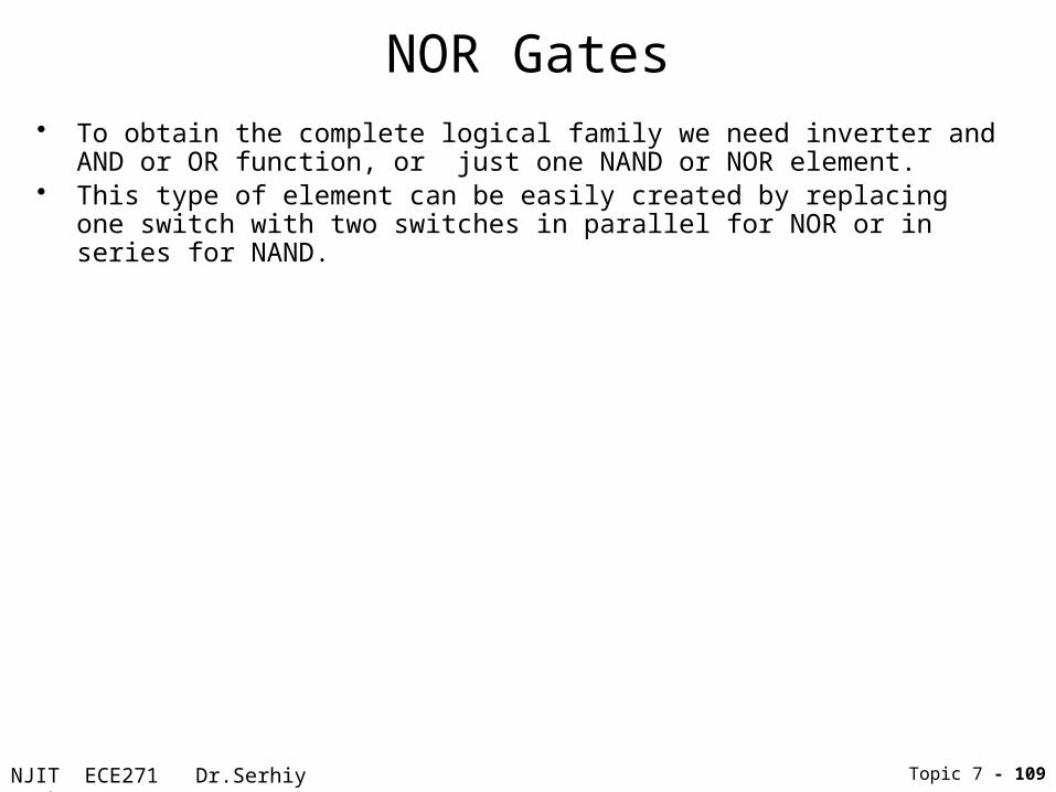
Topic 7 - 108
• To obtain the complete logical family we need inverter and AND or OR function, or just one NAND or NOR element.
NJIT ECE271 Dr.Serhiy Levkov
NOR Gates
Topic 7 - 109
• To obtain the complete logical family we need inverter and AND or OR function, or just one NAND or NOR element.
• This type of element can be easily created by replacing one switch with two switches in parallel for NOR or in series for NAND.

NJIT ECE271 Dr.Serhiy Levkov
NOR Gates
Topic 7 - 110
• To obtain the complete logical family we need inverter and AND or OR function, or just one NAND or NOR element.
• This type of element can be easily created by replacing one switch with two switches in parallel for NOR or in series for NAND.

NJIT ECE271 Dr.Serhiy Levkov
NOR Gates
Topic 7 - 111
• To obtain the complete logical family we need inverter and AND or OR function, or just one NAND or NOR element.
• This type of element can be easily created by replacing one switch with two switches in parallel for NOR or in series for NAND.

NJIT ECE271 Dr.Serhiy Levkov
NOR Gates
Topic 7 - 112
• To obtain the complete logical family we need inverter and AND or OR function, or just one NAND or NOR element.
• This type of element can be easily created by replacing one switch with two switches in parallel for NOR or in series for NAND.

NJIT ECE271 Dr.Serhiy Levkov
NOR Gates
Topic 7 - 113
• To obtain the complete logical family we need inverter and AND or OR function, or just one NAND or NOR element.
• This type of element can be easily created by replacing one switch with two switches in parallel for NOR or in series for NAND.
NJIT ECE271 Dr.Serhiy Levkov
NOR Gates
Topic 7 - 114
• To obtain the complete logical family we need inverter and AND or OR function, or just one NAND or NOR element.
• This type of element can be easily created by replacing one switch with two switches in parallel for NOR or in series for NAND.

NJIT ECE271 Dr.Serhiy Levkov
NOR Gates
Topic 7 - 115
• To obtain the complete logical family we need inverter and AND or OR function, or just one NAND or NOR element.
• This type of element can be easily created by replacing one switch with two switches in parallel for NOR or in series for NAND.
• The worst condition for the output low (to have it as low as possible) is when only one switch is closed (since Ron for both are in parallel).

NJIT ECE271 Dr.Serhiy Levkov
NOR Gates
Topic 7 - 116
• To obtain the complete logical family we need inverter and AND or OR function, or just one NAND or NOR element.
• This type of element can be easily created by replacing one switch with two switches in parallel for NOR or in series for NAND.
• The worst condition for the output low (to have it as low as possible) is when only one switch is closed (since Ron for both are in parallel).
• Thus the M/L ratio should be chosen the same as for one switch.
NJIT ECE271 Dr.Serhiy Levkov
NOR Gates
Topic 7 - 117
• To obtain the complete logical family we need inverter and AND or OR function, or just one NAND or NOR element.
• This type of element can be easily created by replacing one switch with two switches in parallel for NOR or in series for NAND.
• The worst condition for the output low (to have it as low as possible) is when only one switch is closed (since Ron for both are in parallel).
• Thus the M/L ratio should be chosen the same as for one switch. • When both are closed, the VL at the output will be even lower then for one.

NJIT ECE271 Dr.Serhiy Levkov
NAND Gates
Topic 7 - 118
NJIT ECE271 Dr.Serhiy Levkov
NAND Gates
Topic 7 - 119
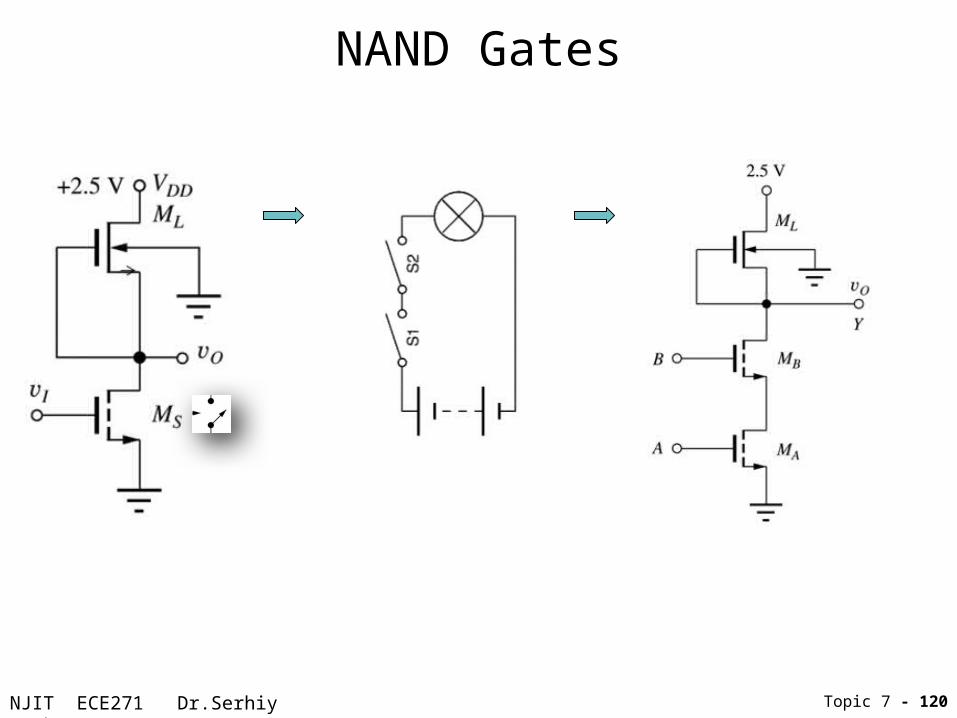
NJIT ECE271 Dr.Serhiy Levkov
NAND Gates
Topic 7 - 120

NJIT ECE271 Dr.Serhiy Levkov
NAND Gate Device Size Selection• Consider the equivalent of switching transistors
in the ‘on” state as Ron.
Topic 7 - 121

NJIT ECE271 Dr.Serhiy Levkov
NAND Gate Device Size Selection• Consider the equivalent of switching transistors
in the ‘on” state as Ron.
• To keep the low voltage level comparable with simple inverter, the desired Ron of MA and MB
must be 0.5Ron of MS switch.
Topic 7 - 122

NJIT ECE271 Dr.Serhiy Levkov
NAND Gate Device Size Selection• Consider the equivalent of switching transistors
in the ‘on” state as Ron.
• To keep the low voltage level comparable with simple inverter, the desired Ron of MA and MB
must be 0.5Ron of MS switch.
• This can be accomplished by approximately doubling (W/L)A and (W/L)B
Topic 7 - 123

NJIT ECE271 Dr.Serhiy Levkov
NAND Gate Device Size Selection• Consider the equivalent of switching transistors
in the ‘on” state as Ron.
• To keep the low voltage level comparable with simple inverter, the desired Ron of MA and MB
must be 0.5Ron of MS switch.
• This can be accomplished by approximately doubling (W/L)A and (W/L)B
Topic 7 - 124

NJIT ECE271 Dr.Serhiy Levkov
NAND Gate Device Size Selection (cont) • Two sources of error that arise are that 1) VSB’s and 2) VGS’s of the two transistors
are not equal the values of VTN should be adjusted (see problem 6.28)
• The technique used to calculate the size of the load transistor for the NAND gate is exactly the same as for the depletion-load inverter.
Topic 7 - 125

NJIT ECE271 Dr.Serhiy Levkov
• An advantage of NMOS technology is that it is simple to design complex logic functions based on the NOR and NAND gates.
Topic 7 - 126
Complex NMOS Logic Design

NJIT ECE271 Dr.Serhiy Levkov
• An advantage of NMOS technology is that it is simple to design complex logic functions based on the NOR and NAND gates.
• The typical problem that arises is the transistor sizing.
Topic 7 - 127
Complex NMOS Logic Design

NJIT ECE271 Dr.Serhiy Levkov
• An advantage of NMOS technology is that it is simple to design complex logic functions based on the NOR and NAND gates.
• The typical problem that arises is the transistor sizing.
• There are two ways to find the W/L ratios of the switching transistors
1) Use the worst-case path (most devices in series) and choose the W/L ratios to achieve the value of Ron
equivalent to that of the inverter
Topic 7 - 128
Complex NMOS Logic Design

NJIT ECE271 Dr.Serhiy Levkov
• An advantage of NMOS technology is that it is simple to design complex logic functions based on the NOR and NAND gates.
• The typical problem that arises is the transistor sizing.
• There are two ways to find the W/L ratios of the switching transistors
1) Use the worst-case path (most devices in series) and choose the W/L ratios to achieve the value of Ron
equivalent to that of the inverter2) Partitioning the circuit into a series sub-networks, and
make the equivalent on-resistances equal
Topic 7 - 129
Complex NMOS Logic Design

NJIT ECE271 Dr.Serhiy Levkov
Complex NMOS Logic Design (1)
Example 1. Design a logic function:
Y = A + B(C + D)
Base inverter:
Topic 7 - 130

NJIT ECE271 Dr.Serhiy Levkov
Complex NMOS Logic Design (1)
Example 1. Design a logic function:
Y = A + B(C + D)
Base inverter:
Topic 7 - 131
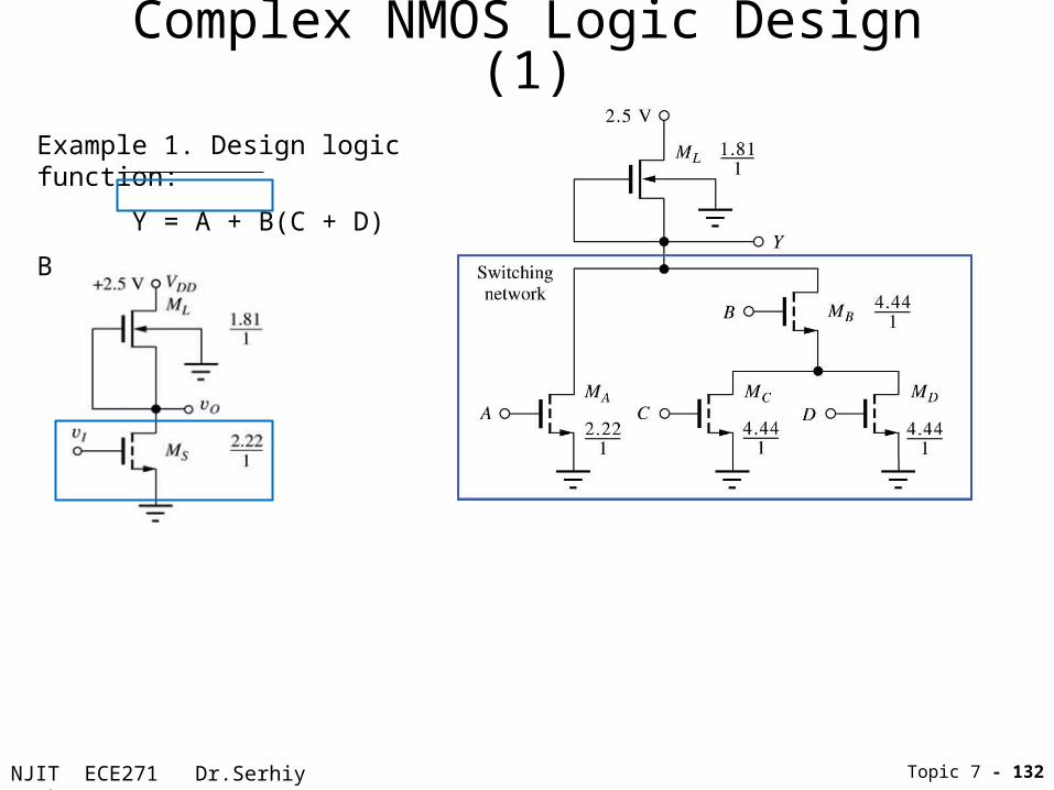
NJIT ECE271 Dr.Serhiy Levkov
Complex NMOS Logic Design (1)
Example 1. Design logic function:
Y = A + B(C + D)
Base inverter:
Topic 7 - 132

NJIT ECE271 Dr.Serhiy Levkov
Complex NMOS Logic Design (1)
Example 1. Design logic function:
Y = A + B(C + D)
Base inverter:
Topic 7 - 133
• Referring to the base inverter design, we have for the MS W/L=2.22/1 in order to maintain the low output of 0.20V

NJIT ECE271 Dr.Serhiy Levkov
Complex NMOS Logic Design (1)
Example 1. Design logic function:
Y = A + B(C + D)
Base inverter:
Topic 7 - 134
• Referring to the base inverter design, we have for the MS W/L=2.22/1 in order to maintain the low output of 0.20V
• We’ll have the same for MA (in parallel).

NJIT ECE271 Dr.Serhiy Levkov
Complex NMOS Logic Design (1)
Example 1. Design logic function:
Y = A + B(C + D)
Base inverter:
Topic 7 - 135
• Referring to the base inverter design, we have for the MS W/L=2.22/1 in order to maintain the low output of 0.20V
• We’ll have the same for MA (in parallel).• In another parallel branch we have a series connection, so MB and combination of
MC and MD should have double width W/L=4.44/1

NJIT ECE271 Dr.Serhiy Levkov
Complex NMOS Logic Design (1)
Example 1. Design logic function:
Y = A + B(C + D)
Base inverter:
Topic 7 - 136
• Referring to the base inverter design, we have for the MS W/L=2.22/1 in order to maintain the low output of 0.20V
• We’ll have the same for MA (in parallel).• In another parallel branch we have a series connection, so MB and combination of
MC and MD should have double width W/L=4.44/1• Finally, MC and MD are in parallel, so their W/L does not change.

NJIT ECE271 Dr.Serhiy Levkov Topic 7 - 137
Complex NMOS Logic Design (2)Example 2. Design logic function:
Y = A B + CDB = (A+CD)B
Base inverter :
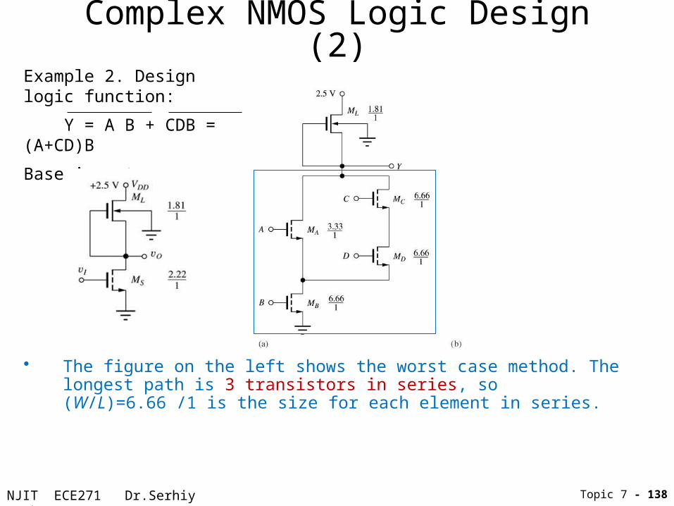
NJIT ECE271 Dr.Serhiy Levkov Topic 7 - 138
Complex NMOS Logic Design (2)Example 2. Design logic function:
Y = A B + CDB = (A+CD)B
Base inverter :
• The figure on the left shows the worst case method. The longest path is 3 transistors in series, so (W/L)=6.66 /1 is the size for each element in series.

NJIT ECE271 Dr.Serhiy Levkov Topic 7 - 139
Complex NMOS Logic Design (2)Example 2. Design logic function:
Y = A B + CDB = (A+CD)B
Base inverter :
• The figure on the left shows the worst case method. The longest path is 3 transistors in series, so (W/L)=6.66 /1 is the size for each element in series. One MA is in parallel with two transistors, so its W/L is halved.

NJIT ECE271 Dr.Serhiy Levkov Topic 7 - 140
Complex NMOS Logic Design (2)Example 2. Design logic function:
Y = A B + CDB = (A+CD)B
Base inverter :
• The figure on the left shows the worst case method. The longest path is 3 transistors in series, so (W/L)=6.66 /1 is the size for each element in series. One MA is in parallel with two transistors, so its W/L is halved.
• The figure on the right shows the partitioning technique : the longest path is 2, so (W/L)= 4.44/1.

NJIT ECE271 Dr.Serhiy Levkov Topic 7 - 141
Complex NMOS Logic Design (2)Example 2. Design logic function:
Y = A B + CDB = (A+CD)B
Base inverter :
• The figure on the left shows the worst case method. The longest path is 3 transistors in series, so (W/L)=6.66 /1 is the size for each element in series. One MA is in parallel with two transistors, so its W/L is halved.
• The figure on the right shows the partitioning technique : the longest path is 2, so (W/L)= 4.44/1. However, now we put 2 series transistors MC and MD in parallel with MA , so their with is doubled.
NJIT ECE271 Dr.Serhiy Levkov
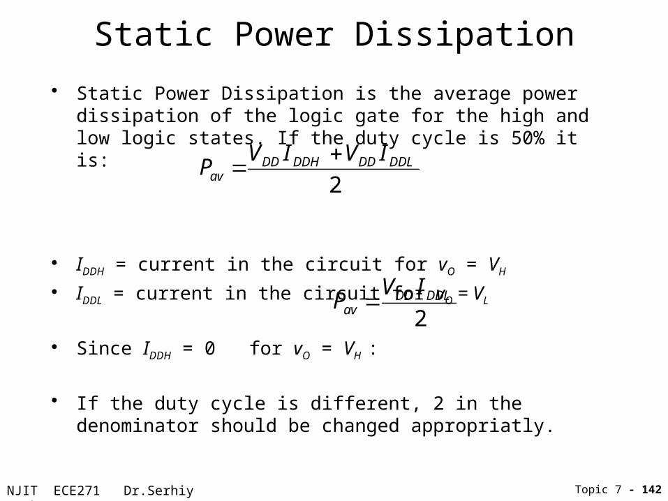
Static Power Dissipation
• Static Power Dissipation is the average power dissipation of the logic gate for the high and low logic states. If the duty cycle is 50% it is:
• IDDH = current in the circuit for vO = VH
• IDDL = current in the circuit for vO = VL
• Since IDDH = 0 for vO = VH :
• If the duty cycle is different, 2 in the denominator should be changed appropriatly.
2DDLDDDDHDD
av
IVIVP
2DDLDD
av
IVP
Topic 7 - 142

NJIT ECE271 Dr.Serhiy Levkov
Dynamic Power Dissipation
• Dynamic Power Dissipation is the power dissipated during the process of charging and discharging the load capacitance connected to the logic gate
DischargingCharging
Topic 7 - 143
??

NJIT ECE271 Dr.Serhiy Levkov
Dynamic Power Dissipation
• Dynamic Power Dissipation is the power dissipated during the process of charging and discharging the load capacitance connected to the logic gate
DischargingCharging
Topic 7 - 144
RL

NJIT ECE271 Dr.Serhiy Levkov
Dynamic Power Dissipation
• Dynamic Power Dissipation is the power dissipated during the process of charging and discharging the load capacitance connected to the logic gate
DischargingCharging
Topic 7 - 145
RS

NJIT ECE271 Dr.Serhiy Levkov
Dynamic Power Dissipation
• Dynamic Power Dissipation is the power dissipated during the process of charging and discharging the load capacitance connected to the logic gate
DischargingCharging
Topic 7 - 146
RL
RS

NJIT ECE271 Dr.Serhiy Levkov
Dynamic Power Dissipation• Based on the energy equation, the energy delivered to the capacitor can be
found by:( ) ( )
2
0 (0) (0)
( )C C
C C
V V
CD DD DD DD C DD
V V
dvE V i t dt V C dt CV dv CV
dt
Topic 7 - 147

NJIT ECE271 Dr.Serhiy Levkov
Dynamic Power Dissipation• Based on the energy equation, the energy delivered to the capacitor can be
found by:
• The energy stored by the capacitor is:
( ) ( )2
0 (0) (0)
( )C C
C C
V V
CD DD DD DD C DD
V V
dvE V i t dt V C dt CV dv CV
dt
2
2DD
D
CVE
Topic 7 - 148

NJIT ECE271 Dr.Serhiy Levkov
Dynamic Power Dissipation• Based on the energy equation, the energy delivered to the capacitor can be
found by:
• The energy stored by the capacitor is:
• The energy lost in the resistive elements is given by:
( ) ( )2
0 (0) (0)
( )C C
C C
V V
CD DD DD DD C DD
V V
dvE V i t dt V C dt CV dv CV
dt
2
2DD
S
CVE
2
2DD
SDL
CVEEE
Topic 7 - 149

NJIT ECE271 Dr.Serhiy Levkov
Dynamic Power Dissipation• Based on the energy equation, the energy delivered to the capacitor can be
found by:
• The energy stored by the capacitor is:
• The energy lost in the resistive elements is given by:
• The total energy lost in the first charging and discharging of the capacitor through resistive elements is given by:
( ) ( )2
0 (0) (0)
( )C C
C C
V V
CD DD DD DD C DD
V V
dvE V i t dt V C dt CV dv CV
dt
2
2DD
D
CVE
2
2DD
SDL
CVEEE
Topic 7 - 150
222
22 DDDDDD
TD CVCVCV
E

NJIT ECE271 Dr.Serhiy Levkov
Dynamic Power Dissipation• Based on the energy equation, the energy delivered to the capacitor can be
found by:
• The energy stored by the capacitor is:
• The energy lost in the resistive elements is given by:
• The total energy lost in the first charging and discharging of the capacitor through resistive elements is given by:
• Thus, if the logic circuit is switching at a frequency f, the dynamic power dissipation is given by:
( ) ( )2
0 (0) (0)
( )C C
C C
V V
CD DD DD DD C DD
V V
dvE V i t dt V C dt CV dv CV
dt
2
2DD
D
CVE
2
2DD
SDL
CVEEE
Topic 7 - 151
222
22 DDDDDD
TD CVCVCV
E
fCVP DDD2

NJIT ECE271 Dr.Serhiy Levkov
Dynamic Power Dissipation• Based on the energy equation, the energy delivered to the capacitor can be
found by:
• The energy stored by the capacitor is:
• The energy lost in the resistive elements is given by:
• The total energy lost in the first charging and discharging of the capacitor through resistive elements is given by:
• Thus, if the logic circuit is switching at a frequency f, the dynamic power dissipation is given by:
• In the high speed logic circuits this component becomes dominant and constitutes the primary source of power dissipation in CMOS logic gates.
( ) ( )2
0 (0) (0)
( )C C
C C
V V
CD DD DD DD C DD
V V
dvE V i t dt V C dt CV dv CV
dt
2
2DD
D
CVE
2
2DD
SDL
CVEEE
Topic 7 - 152
222
22 DDDDDD
TD CVCVCV
E
fCVP DDD2

NJIT ECE271 Dr.Serhiy Levkov
Power Scaling in MOS Logic
• With the transistor load, the current in both the load and switch transistors is determined by the similar expressions, e.g.:
• By reducing the W/L of the load and switching transistors of an inverter, it is possible to reduce the power dissipation by the same factor without sacrificing VH and VL.
• This same concept works for increasing the power which will increase the dynamic response.
Topic 7 - 153

NJIT ECE271 Dr.Serhiy Levkov
Power Scaling in MOS Logic
a) Original Saturated Load Inverterb) Saturated Load inverter designed to operate at 1/3 the powerc) Original Depletion-Mode Inverterd) Depletion-mode inverter designed to operate at twice the power
Topic 7 - 154

NJIT ECE271 Dr.Serhiy Levkov
Dynamic BehaviorCapacitance in MOS Logic Circuits
• The MOS device has capacitances CSB, CGS, CDB, and CGD that need to be considered for dynamic response analysis.
Topic 7 - 155

NJIT ECE271 Dr.Serhiy Levkov
Dynamic BehaviorCapacitance in MOS Logic Circuits
• The MOS device has capacitances CSB, CGS, CDB, and CGD that need to be considered for dynamic response analysis.
• The capacitances seen at a node can be lumped together.
Topic 7 - 156

NJIT ECE271 Dr.Serhiy Levkov
Dynamic BehaviorCapacitance in MOS Logic Circuits
• The MOS device has capacitances CSB, CGS, CDB, and CGD that need to be considered for dynamic response analysis.
• The capacitances seen at a node can be lumped together.• DC loading constraints are not usually important for MOS logic circuits since they
normally drive capacitive loads (i.e. the gate of a MOS)
Topic 7 - 157

NJIT ECE271 Dr.Serhiy Levkov
Dynamic BehaviorCapacitance in MOS Logic Circuits
• The MOS device has capacitances CSB, CGS, CDB, and CGD that need to be considered for dynamic response analysis.
• The capacitances seen at a node can be lumped together.• DC loading constraints are not usually important for MOS logic circuits since they
normally drive capacitive loads (i.e. the gate of a MOS)• As the number of gates the output (fan-out) of a logic device has to drive increases, the
load capacitance increases, and the time response degrades.
Topic 7 - 158

NJIT ECE271 Dr.Serhiy Levkov
Dynamic BehaviorCapacitance in MOS Logic Circuits
• The MOS device has capacitances CSB, CGS, CDB, and CGD that need to be considered for dynamic response analysis.
• The capacitances seen at a node can be lumped together.• DC loading constraints are not usually important for MOS logic circuits since they
normally drive capacitive loads (i.e. the gate of a MOS)• As the number of gates the output (fan-out) of a logic device has to drive increases, the
load capacitance increases, and the time response degrades.• This notion implies that the fan-out that a logic circuit can drive will be limited by
time delay tolerances of the circuit.
Topic 7 - 159

NJIT ECE271 Dr.Serhiy Levkov
Dynamic Response of the NMOS Inverter with a Resistive Load
• Rise time is defined as the time for the output to change from 10% to 90% of the complete transition.
1 11 1
2 12 2
2 1
( ) exp 0.1 exp 0.9 ln 0.9
( ) exp 0.9 exp 0.1 ln 0.1
( ln 0.1 ln .9) ln(0.9 / 0.1) ln 9 2
O F I
O F I
r
t tv t V V V V V V t RC
RC RC
t tv t V V V V V V t RC
RC RC
t t t RC RC RC
.2RC
Topic 7 - 160
Closing switch: vI high low Charging capacitor
NJIT ECE271 Dr.Serhiy Levkov
Dynamic Response of the NMOS Inverter with a Resistive Load
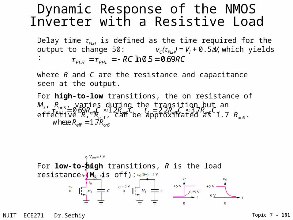
Delay time τPLH is defined as the time required for the output to change 50: vO(τPLH) = VI + 0.5V, which yields :
ln 0.5 0.69PLH PHL RC RC
where R and C are the resistance and capacitance seen at the output.
For high-to-low transitions, the on resistance of MS, RonS, varies during the transition but an effective R, Reff, can be approximated as 1.7 RonS.
For low-to-high transitions, R is the load resistance (MS is off):
eff eff
eff
0.69 1.2 2.2 3.7 ,
where 1.7
PHL onS f onS
onS
R C R C t R C R C
R R
Topic 7 - 161

NJIT ECE271 Dr.Serhiy Levkov
Pseudo NMOS Inverter - Dynamic Response
PHL 0.69ReffC 1.2RonSC
t f 2.2ReffC 3.7RonSC,
PLH 0.69ReffC 1.2RonLC
tr 2.2ReffC 3.7RonLC,
Topic 7 - 162
• The expressions for the propagation delays are the same as for resistive
Closing switch: vI high low Opening switch: vI low high
NJIT ECE271 Dr.Serhiy Levkov
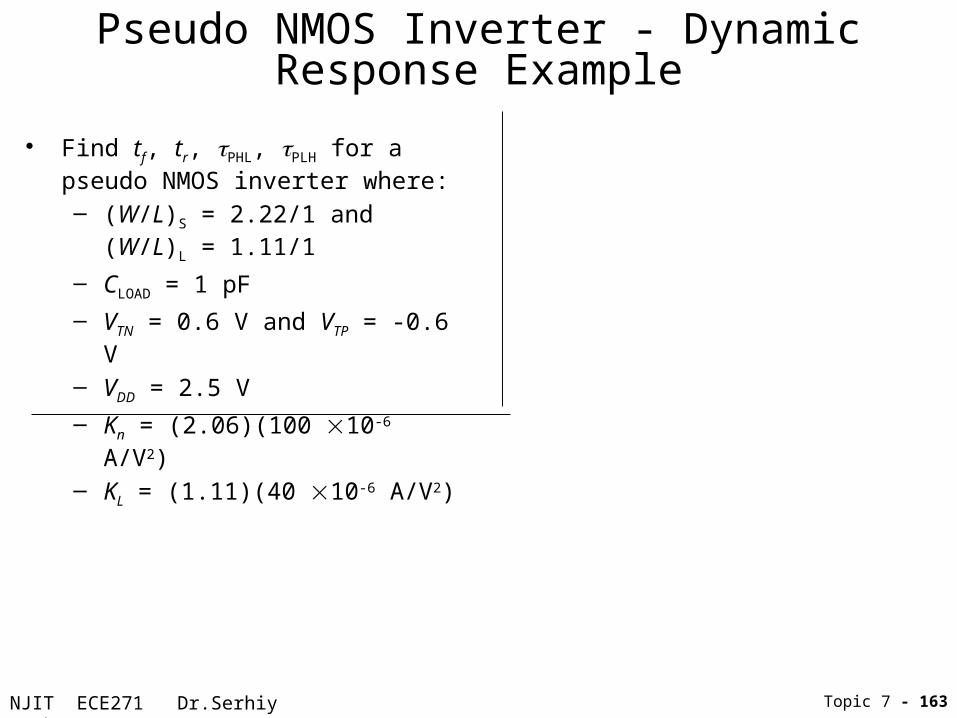
Pseudo NMOS Inverter - Dynamic Response Example
• Find tf, tr, PHL, PLH for a pseudo NMOS inverter where:– (W/L)S = 2.22/1 and (W/L)L = 1.11/1
– CLOAD = 1 pF
– VTN = 0.6 V and VTP = -0.6 V
– VDD = 2.5 V
– Kn = (2.06)(100 10-6 A/V2)
– KL = (1.11)(40 10-6 A/V2)
Topic 7 - 163

NJIT ECE271 Dr.Serhiy Levkov
Pseudo NMOS Inverter - Dynamic Response Example
• Find tf, tr, PHL, PLH for a pseudo NMOS inverter where:– (W/L)S = 2.22/1 and (W/L)L = 1.11/1
– CLOAD = 1 pF
– VTN = 0.6 V and VTP = -0.6 V
– VDD = 2.5 V
– Kn = (2.06)(100 10-6 A/V2)
– KL = (1.11)(40 10-6 A/V2)
Topic 7 - 164
• First find the on-resistances of the two switch and load devices
2
2
1 12.37
2.22 100 2.5 0.6
1 111.9
| |1.11 40 | 2.5 ( 0.6) |
onSS H TNS
onLL DD TP
R kAK V V
V
R kAK V V
V
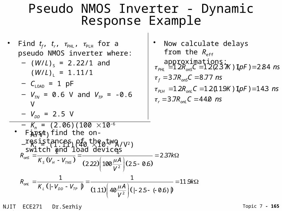
NJIT ECE271 Dr.Serhiy Levkov
Pseudo NMOS Inverter - Dynamic Response Example
• Find tf, tr, PHL, PLH for a pseudo NMOS inverter where:– (W/L)S = 2.22/1 and (W/L)L = 1.11/1
– CLOAD = 1 pF
– VTN = 0.6 V and VTP = -0.6 V
– VDD = 2.5 V
– Kn = (2.06)(100 10-6 A/V2)
– KL = (1.11)(40 10-6 A/V2)
Topic 7 - 165
• First find the on-resistances of the two switch and load devices
2
2
1 12.37
2.22 100 2.5 0.6
1 111.9
| |1.11 40 | 2.5 ( 0.6) |
onSS H TNS
onLL DD TP
R kAK V V
V
R kAK V V
V
• Now calculate delays from the Reff approximations:
PHL 1.2RonSC 1.2(2.37K)(1pF )2.84 ns
f 3.7RonSC 8.77 ns
PLH 1.2RonLC 1.2(11.9K)(1pF)14.3 ns
r 3.7RonLC 44.0 ns

NJIT ECE271 Dr.Serhiy Levkov
Comparison of Load Devices
The simulation results for all five inverters. The current has been normalized to 80 A for vo = VOL= 0.20 V
Topic 7 - 166
• The saturated load devices have the poorest fall time since they have the lowest load current delivery
• The saturated load devices also reach zero current before the output reaches 2.5 V• The linear load device is faster than the saturated load device, but about equal to
the resistive load speed.• The fastest PLH is for the pseudo NMOS device as a result of the PMOS device

NJIT ECE271 Dr.Serhiy Levkov
PMOS Logic
• PMOS logic circuits predated NMOS logic circuit, but were replaced since they operate at slower speeds
Resistive Load Saturated Load Linear Load Depletion-Mode Load
Pseudo PMOS
Topic 7 - 167

NJIT ECE271 Dr.Serhiy Levkov
PMOS NAND and NOR Gates
NOR Gate NAND Gate
Topic 7 - 168
Related Documents