HAL Id: hal-00646462 https://hal.archives-ouvertes.fr/hal-00646462 Submitted on 30 Nov 2011 HAL is a multi-disciplinary open access archive for the deposit and dissemination of sci- entific research documents, whether they are pub- lished or not. The documents may come from teaching and research institutions in France or abroad, or from public or private research centers. L’archive ouverte pluridisciplinaire HAL, est destinée au dépôt et à la diffusion de documents scientifiques de niveau recherche, publiés ou non, émanant des établissements d’enseignement et de recherche français ou étrangers, des laboratoires publics ou privés. Design of a high voltage input - output ratio dc-dc converter dedicated to small power fuel cell systems O. Béthoux, J. Cathelin To cite this version: O. Béthoux, J. Cathelin. Design of a high voltage input - output ratio dc-dc converter dedicated to small power fuel cell systems. European Physical Journal: Applied Physics, EDP Sciences, 2010, 52 (3), 10.1051/epjap/2010148. hal-00646462

Welcome message from author
This document is posted to help you gain knowledge. Please leave a comment to let me know what you think about it! Share it to your friends and learn new things together.
Transcript
HAL Id: hal-00646462https://hal.archives-ouvertes.fr/hal-00646462
Submitted on 30 Nov 2011
HAL is a multi-disciplinary open accessarchive for the deposit and dissemination of sci-entific research documents, whether they are pub-lished or not. The documents may come fromteaching and research institutions in France orabroad, or from public or private research centers.
L’archive ouverte pluridisciplinaire HAL, estdestinée au dépôt et à la diffusion de documentsscientifiques de niveau recherche, publiés ou non,émanant des établissements d’enseignement et derecherche français ou étrangers, des laboratoirespublics ou privés.
Design of a high voltage input - output ratio dc-dcconverter dedicated to small power fuel cell systems
O. Béthoux, J. Cathelin
To cite this version:O. Béthoux, J. Cathelin. Design of a high voltage input - output ratio dc-dc converter dedicated tosmall power fuel cell systems. European Physical Journal: Applied Physics, EDP Sciences, 2010, 52(3), 10.1051/epjap/2010148. hal-00646462
1
DESIGN OF A HIGH VOLTAGE INPUT – OUTPUT RATIO DC-DC CONVERTER
DEDICATED TO SMALL POWER FUEL CELL SYSTEMS
O. Béthoux *, J . Cathelin *
* Laboratoire de Génie Electrique de Paris (LGEP) / SPEE-Labs, CNRS UMR 8507; SUPELEC; Université Pierre et Marie Curie P6; Université Paris-Sud 11; 11 rue Joliot Curie, Plateau de Moulon F91192 Gif sur Yvette CEDEX
Keywords: fuel cell, power electronics, DC-DC power conversion,, efficiency, semiconductor stress, soft switching, experimental validation.
Abstract
Consuming chemical energy, fuel cells produce simultaneously heat, water and useful electrical power [1] [2]. As a matter of fact, the voltage generated by a fuel cell strongly depends on both the load power demand and the operating conditions. Besides, as a result of many design aspects, fuel cells are low voltage and high current electric generators. On the contrary, electric loads are commonly designed for small voltage swing and a high V/I ratio in order to minimize Joule losses. Therefore, electric loads supplied by fuel cells are typically fed by means of an intermediate power voltage regulator. The specifications of such a power converter are to be able to step up the input voltage with a high ratio (a ratio of 10 is a classic situation) and also to work with an excellent efficiency (in order to minimize its size, its weight and its losses) [3].
This paper deals with the design of this essential ancillary device. It intends to bring out the best structure for fulfilling this function. Several DC-DC converters with large voltage step-up ratios are introduced. A topology based on a coupled-inductor or tapped-inductor is closely studied. A detailed modelling is performed with the purpose of providing designing rules. This model is validated with both simulation and implementation.
The experimental prototype is based on the following specifications: the fuel cell output voltage ranges from a 50 V open-voltage to a 25 V rated voltage while the load requires a constant 250 V voltage. The studied coupled-inductor converter is compared with a classic boost converter commonly used in this voltage elevating application. Even though the voltage regulator faces severe FC specifications, the measured efficiency reaches 96 % at the rated power whereas conventional boost efficiency barely achieves 91.5 % in the same operating conditions.
1 Introduction
Since the 19th, industrial expansion has always leaned on intensive use of fossil resources: coal, oil and natural gas [4]. At the beginning of the 21st century, governments gradually become aware of the limit of the hydrocarbon reserves [5]. On top of a secure and sustainable long-term energy supply, the huge use of hydrocarbon resources already proved to have negative impact on the earth environmental equilibrium. As a matter of fact, greenhouse gases such as carbon dioxide and methane have deeply and suddenly increased leading to a previous unknown situation [6]. For these two main reasons, finding out new energy alternatives has become a key issue of this century. In this context, hydrogen has attracted great attention in the recent years as a new and clean energy carrier. Hydrogen avoids the dependency and depletion of fossil fuels because it can be produced by different means and especially thanks to renewable resources (wind, sun …) [7]. Furthermore, hydrogen has a good energy specific gravity (120 MJ/kg); no toxic gas is generated during its combustion, particularly in the case of the electrochemical oxidation and reduction reactions taking place in fuel cells; residue is only water and heat [8]. Therefore, fuel cells (FCs) are the most important field of the "hydrogen-energy" use. Theirs areas of application are various. It provides electric power to portable electronic devices, communication equipments, spacecraft power systems (electricity and water cogeneration), transport systems (cars, boats, and planes), and also buildings (electricity and warmth cogeneration), in a range of power from a few watts to hundred kilowatts.
However, FC is not an ideal voltage generator and the FC voltage becomes smaller as far as the load power demand increases. Indeed, the FC voltage-current relationship is induced by the three main irreversible losses that occur in the FC processes. Activation polarization (∆Vact) is the irreversible voltage loss associated with overcoming the energy barrier to the electrode reaction and cathode (air) kinetic limitations dominate in this ∆Vact term. Ohmic losses are basically due to ionic current in the electrolyte whereas collector resistance and contact resistance (electronic current) are negligible. It induces an ohmic polarization (∆Vohm). Transport mechanisms within the gas diffusion layer and electrode structure cause a reactant concentration decrease at
2
the electrode surface and produce an irreversible voltage loss named concentration polarization (∆Vcon) [9]. As a conclusion, the actual fuel cell voltage (VFC) at any given current (IFC) can be represented as the reversible voltage (roughly the open-circuit voltage) minus the activation, ohmic and concentration voltage losses.
conohmactFCFC VVVEV ∆−∆−∆−= (1)
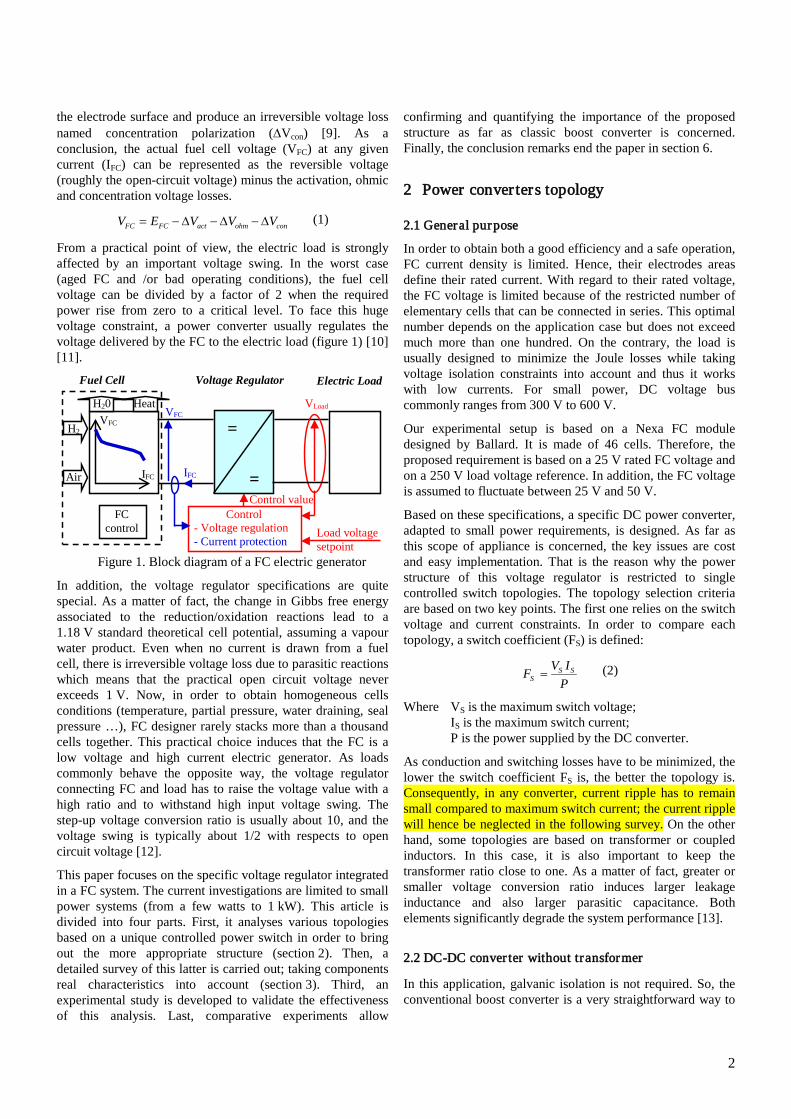
From a practical point of view, the electric load is strongly affected by an important voltage swing. In the worst case (aged FC and /or bad operating conditions), the fuel cell voltage can be divided by a factor of 2 when the required power rise from zero to a critical level. To face this huge voltage constraint, a power converter usually regulates the voltage delivered by the FC to the electric load (figure 1) [10] [11].
Control - Voltage regulation - Current protection
FC control Load voltage
setpoint
VFC
IFC
Fuel Cell
H2 VFC
IFC
=
= Air
Voltage Regulator Electric Load
H20 Heat VLoad
Control value
Figure 1. Block diagram of a FC electric generator
In addition, the voltage regulator specifications are quite special. As a matter of fact, the change in Gibbs free energy associated to the reduction/oxidation reactions lead to a 1.18 V standard theoretical cell potential, assuming a vapour water product. Even when no current is drawn from a fuel cell, there is irreversible voltage loss due to parasitic reactions which means that the practical open circuit voltage never exceeds 1 V. Now, in order to obtain homogeneous cells conditions (temperature, partial pressure, water draining, seal pressure …), FC designer rarely stacks more than a thousand cells together. This practical choice induces that the FC is a low voltage and high current electric generator. As loads commonly behave the opposite way, the voltage regulator connecting FC and load has to raise the voltage value with a high ratio and to withstand high input voltage swing. The step-up voltage conversion ratio is usually about 10, and the voltage swing is typically about 1/2 with respects to open circuit voltage [12].
This paper focuses on the specific voltage regulator integrated in a FC system. The current investigations are limited to small power systems (from a few watts to 1 kW). This article is divided into four parts. First, it analyses various topologies based on a unique controlled power switch in order to bring out the more appropriate structure (section 2). Then, a detailed survey of this latter is carried out; taking components real characteristics into account (section 3). Third, an experimental study is developed to validate the effectiveness of this analysis. Last, comparative experiments allow
confirming and quantifying the importance of the proposed structure as far as classic boost converter is concerned. Finally, the conclusion remarks end the paper in section 6.
2 Power conver ters topology
2.1 General purpose
In order to obtain both a good efficiency and a safe operation, FC current density is limited. Hence, their electrodes areas define their rated current. With regard to their rated voltage, the FC voltage is limited because of the restricted number of elementary cells that can be connected in series. This optimal number depends on the application case but does not exceed much more than one hundred. On the contrary, the load is usually designed to minimize the Joule losses while taking voltage isolation constraints into account and thus it works with low currents. For small power, DC voltage bus commonly ranges from 300 V to 600 V.
Our experimental setup is based on a Nexa FC module designed by Ballard. It is made of 46 cells. Therefore, the proposed requirement is based on a 25 V rated FC voltage and on a 250 V load voltage reference. In addition, the FC voltage is assumed to fluctuate between 25 V and 50 V.
Based on these specifications, a specific DC power converter, adapted to small power requirements, is designed. As far as this scope of appliance is concerned, the key issues are cost and easy implementation. That is the reason why the power structure of this voltage regulator is restricted to single controlled switch topologies. The topology selection criteria are based on two key points. The first one relies on the switch voltage and current constraints. In order to compare each topology, a switch coefficient (FS) is defined:
PIVF SS
S = (2)
Where VS is the maximum switch voltage; IS is the maximum switch current; P is the power supplied by the DC converter.
As conduction and switching losses have to be minimized, the lower the switch coefficient FS is, the better the topology is. Consequently, in any converter, current ripple has to remain small compared to maximum switch current; the current ripple will hence be neglected in the following survey. On the other hand, some topologies are based on transformer or coupled inductors. In this case, it is also important to keep the transformer ratio close to one. As a matter of fact, greater or smaller voltage conversion ratio induces larger leakage inductance and also larger parasitic capacitance. Both elements significantly degrade the system performance [13].
2.2 DC-DC conver ter without transformer
In this application, galvanic isolation is not required. So, the conventional boost converter is a very straightforward way to
3
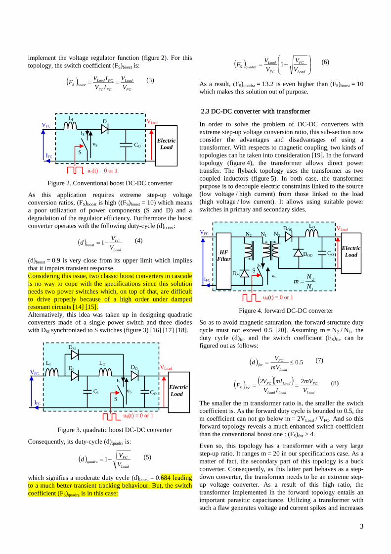
implement the voltage regulator function (figure 2). For this topology, the switch coefficient (FS)boost is:
( )FC
Load
FCFC
FCLoadboostS V
VIVIVF == (3)
VFC
IFC
VLoad
uS(t) = 0 or 1
Electric Load
LI
S
D
CO vS
iS
Figure 2. Conventional boost DC-DC converter
As this application requires extreme step-up voltage conversion ratios, (FS)boost is high ((FS)boost = 10) which means a poor utilization of power components (S and D) and a degradation of the regulator efficiency. Furthermore the boost converter operates with the following duty-cycle (d)boost:
( )Load
FCboost V
Vd −= 1 (4)
(d)boost = 0.9 is very close from its upper limit which implies that it impairs transient response. Considering this issue, two classic boost converters in cascade is no way to cope with the specifications since this solution needs two power switches which, on top of that, are difficult to drive properly because of a high order under damped resonant circuits [14] [15]. Alternatively, this idea was taken up in designing quadratic converters made of a single power switch and three diodes with DSI synchronized to S switches (figure 3) [16] [17] [18].
VFC
IFC
VLoad
uS(t) = 0 or 1
Electric Load
LI
S CO vS
iS
DO
DSI
LO DI
CI
Figure 3. quadratic boost DC-DC converter
Consequently, its duty-cycle (d)quadra is:
( )Load
FCquadra V
Vd −= 1 (5)
which signifies a moderate duty cycle (d)boost = 0.684 leading to a much better transient tracking behaviour. But, the switch coefficient (FS)quadra is in this case:
( )
+=
Load
FC
FC
LoadquadraS V
VVVF 1 (6)
As a result, (FS)quadra = 13.2 is even higher than (FS)boost = 10 which makes this solution out of purpose.
2.3 DC-DC conver ter with transformer
In order to solve the problem of DC-DC converters with extreme step-up voltage conversion ratio, this sub-section now consider the advantages and disadvantages of using a transformer. With respects to magnetic coupling, two kinds of topologies can be taken into consideration [19]. In the forward topology (figure 4), the transformer allows direct power transfer. The flyback topology uses the transformer as two coupled inductors (figure 5). In both case, the transformer purpose is to decouple electric constraints linked to the source (low voltage / high current) from those linked to the load (high voltage / low current). It allows using suitable power switches in primary and secondary sides.
VFC VLoad
uS(t) = 0 or 1
Electric Load
S
CO
vS
iS
DOS LO
DM
DOD
N2 N1 * *
*
IFC
HF Filter
N2
1
2
NNm =
Figure 4. forward DC-DC converter
So as to avoid magnetic saturation, the forward structure duty cycle must not exceed 0.5 [20]. Assuming m = N2 / N1, the duty cycle (d)for and the switch coefficient (FS)for can be figured out as follows:
( ) 5.0≤=Load
FCfor mV
Vd (7)
( ) ( )( )Load
FC
LoadLoad
LoadFCforS V
mVIVmIVF 22
== (8)
The smaller the m transformer ratio is, the smaller the switch coefficient is. As the forward duty cycle is bounded to 0.5, the m coefficient can not go below m = 2VLoad / VFC. And so this forward topology reveals a much enhanced switch coefficient than the conventional boost one : (FS)for > 4.
Even so, this topology has a transformer with a very large step-up ratio. It ranges m = 20 in our specifications case. As a matter of fact, the secondary part of this topology is a buck converter. Consequently, as this latter part behaves as a step-down converter, the transformer needs to be an extreme step-up voltage converter. As a result of this high ratio, the transformer implemented in the forward topology entails an important parasitic capacitance. Utilizing a transformer with such a flaw generates voltage and current spikes and increases
4
dramatically power loss and noise. This drawback makes this solution unfeasible.
VFC
VLoad
uS(t) = 0 or 1
Electric Load
S
CO
vS
iS
D N2 N1
*
*
IFC
HF Filter
1
2
NNm =
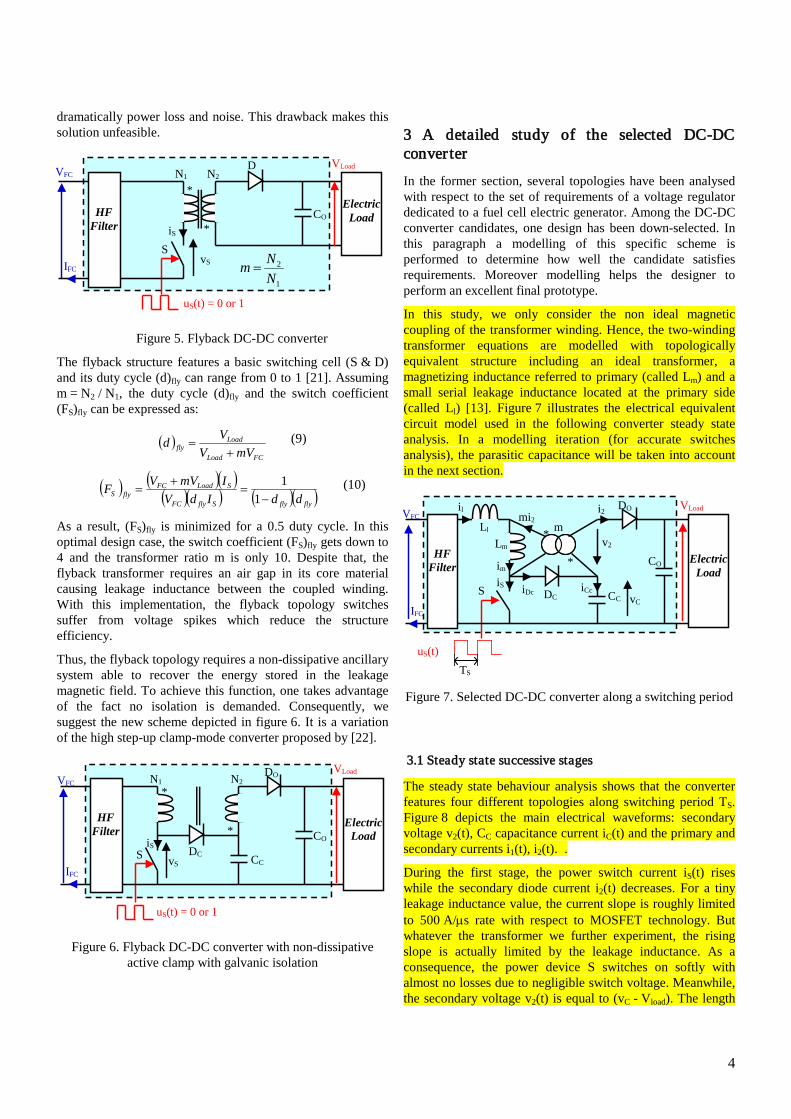
Figure 5. Flyback DC-DC converter
The flyback structure features a basic switching cell (S & D) and its duty cycle (d)fly can range from 0 to 1 [21]. Assuming m = N2 / N1, the duty cycle (d)fly and the switch coefficient (FS)fly can be expressed as:
( )FCLoad
Loadfly mVV
Vd+
= (9)
( ) ( )( )( )( ) ( )( )flyflySflyFC
SLoadFCflyS ddIdV
ImVVF−
=+
=1
1 (10)
As a result, (FS)fly is minimized for a 0.5 duty cycle. In this optimal design case, the switch coefficient (FS)fly gets down to 4 and the transformer ratio m is only 10. Despite that, the flyback transformer requires an air gap in its core material causing leakage inductance between the coupled winding. With this implementation, the flyback topology switches suffer from voltage spikes which reduce the structure efficiency.
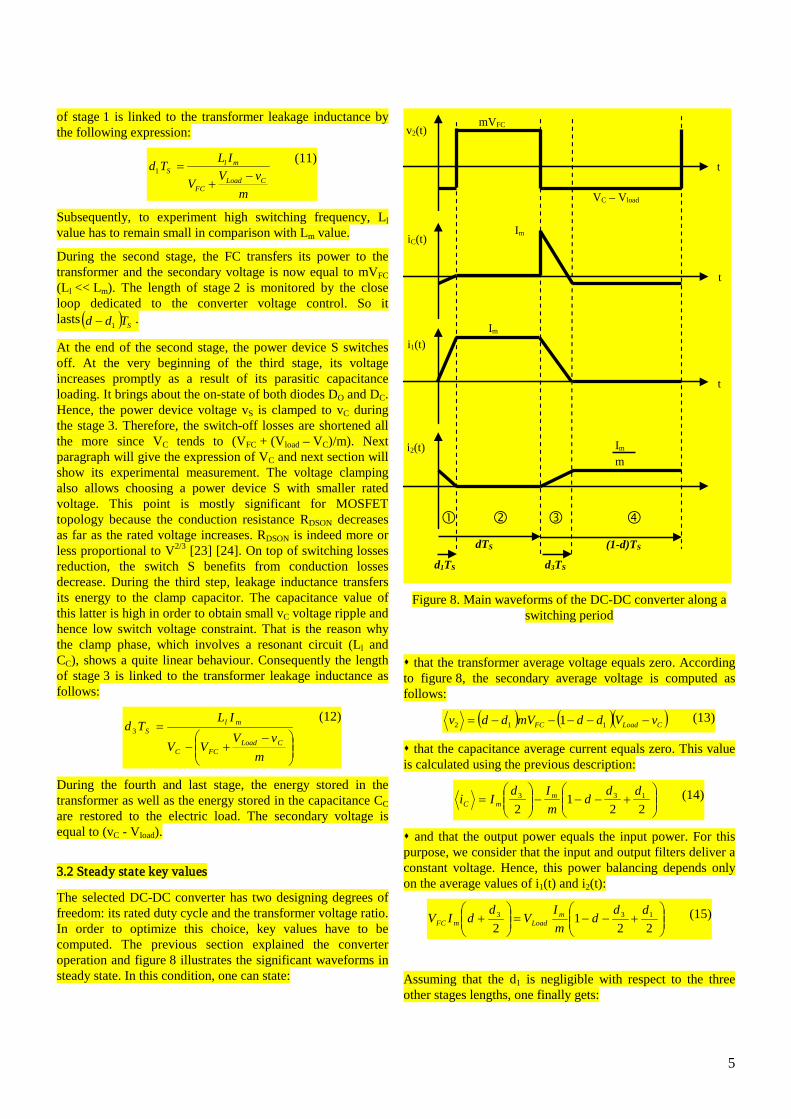
Thus, the flyback topology requires a non-dissipative ancillary system able to recover the energy stored in the leakage magnetic field. To achieve this function, one takes advantage of the fact no isolation is demanded. Consequently, we suggest the new scheme depicted in figure 6. It is a variation of the high step-up clamp-mode converter proposed by [22].
VFC
VLoad
uS(t) = 0 or 1
Electric Load
S CO
vS iS
DO N2 N1
*
*
IFC
HF Filter
CC DC
Figure 6. Flyback DC-DC converter with non-dissipative
active clamp with galvanic isolation
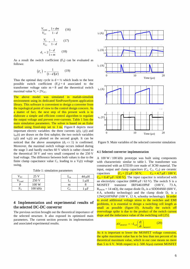
3 A detailed study of the selected DC-DC conver ter
In the former section, several topologies have been analysed with respect to the set of requirements of a voltage regulator dedicated to a fuel cell electric generator. Among the DC-DC converter candidates, one design has been down-selected. In this paragraph a modelling of this specific scheme is performed to determine how well the candidate satisfies requirements. Moreover modelling helps the designer to perform an excellent final prototype.
In this study, we only consider the non ideal magnetic coupling of the transformer winding. Hence, the two-winding transformer equations are modelled with topologically equivalent structure including an ideal transformer, a magnetizing inductance referred to primary (called Lm) and a small serial leakage inductance located at the primary side (called Ll) [13]. Figure 7 illustrates the electrical equivalent circuit model used in the following converter steady state analysis. In a modelling iteration (for accurate switches analysis), the parasitic capacitance will be taken into account in the next section.
VFC
VLoad
uS(t)
Electric Load
S
CO
iS
DO
*
*
IFC
HF Filter
CC DC
TS
m
vC
Lm Ll
iDc iCc
i2
im
il
mi2
v2
Figure 7. Selected DC-DC converter along a switching period
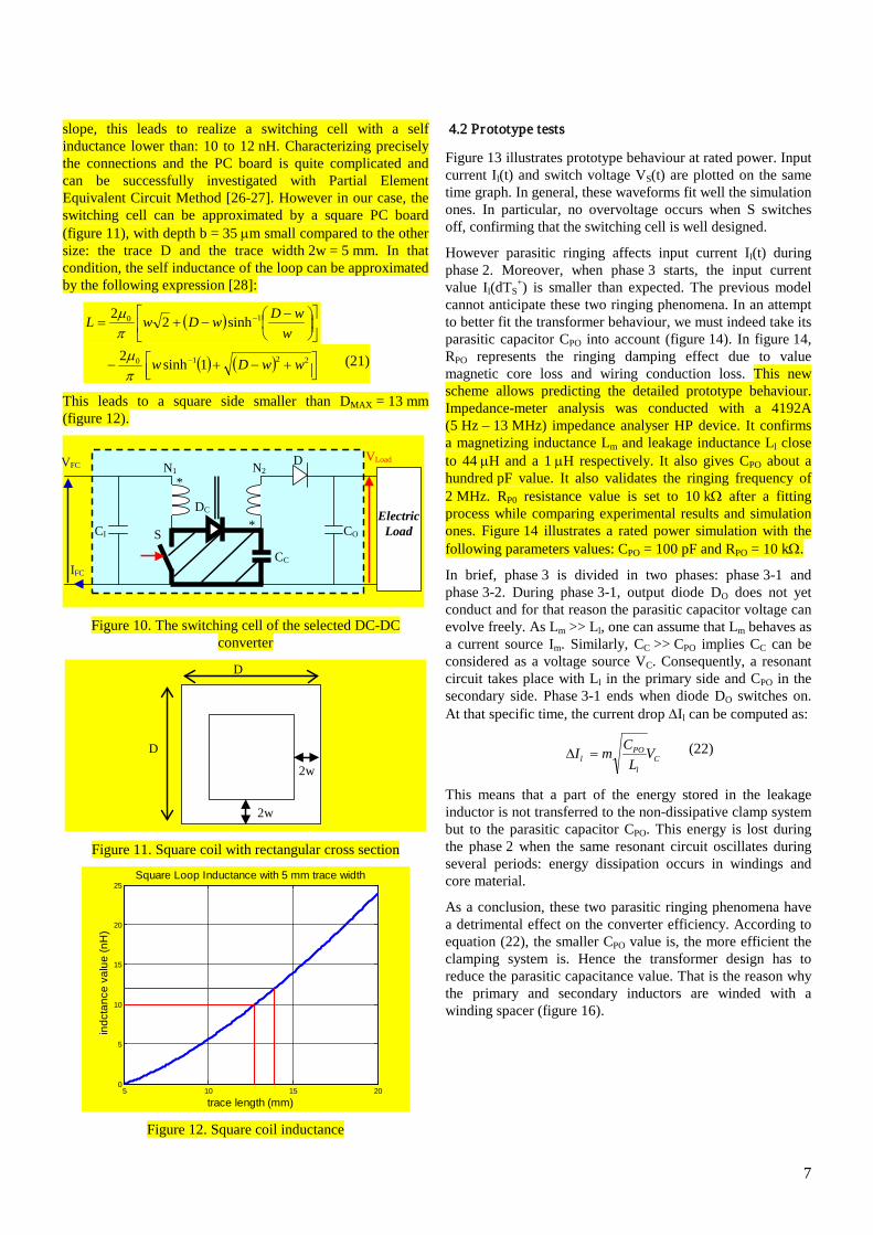
3.1 Steady state successive stages
The steady state behaviour analysis shows that the converter features four different topologies along switching period TS. Figure 8 depicts the main electrical waveforms: secondary voltage v2(t), CC capacitance current iC(t) and the primary and secondary currents i1(t), i2(t). .
During the first stage, the power switch current iS(t) rises while the secondary diode current i2(t) decreases. For a tiny leakage inductance value, the current slope is roughly limited to 500 A/µs rate with respect to MOSFET technology. But whatever the transformer we further experiment, the rising slope is actually limited by the leakage inductance. As a consequence, the power device S switches on softly with almost no losses due to negligible switch voltage. Meanwhile, the secondary voltage v2(t) is equal to (vC - Vload). The length
5
of stage 1 is linked to the transformer leakage inductance by the following expression:
mvVV
ILTdCLoad
FC
mlS −
+=1
(11)
Subsequently, to experiment high switching frequency, Ll value has to remain small in comparison with Lm value.
During the second stage, the FC transfers its power to the transformer and the secondary voltage is now equal to mVFC (Ll << Lm). The length of stage 2 is monitored by the close loop dedicated to the converter voltage control. So it lasts ( ) STdd 1− .
At the end of the second stage, the power device S switches off. At the very beginning of the third stage, its voltage increases promptly as a result of its parasitic capacitance loading. It brings about the on-state of both diodes DO and DC. Hence, the power device voltage vS is clamped to vC during the stage 3. Therefore, the switch-off losses are shortened all the more since VC tends to (VFC + (Vload – VC)/m). Next paragraph will give the expression of VC and next section will show its experimental measurement. The voltage clamping also allows choosing a power device S with smaller rated voltage. This point is mostly significant for MOSFET topology because the conduction resistance RDSON decreases as far as the rated voltage increases. RDSON is indeed more or less proportional to V2/3 [23] [24]. On top of switching losses reduction, the switch S benefits from conduction losses decrease. During the third step, leakage inductance transfers its energy to the clamp capacitor. The capacitance value of this latter is high in order to obtain small vC voltage ripple and hence low switch voltage constraint. That is the reason why the clamp phase, which involves a resonant circuit (Ll and CC), shows a quite linear behaviour. Consequently the length of stage 3 is linked to the transformer leakage inductance as follows:
−+−
=
mvV
VV
ILTd
CLoadFCC
mlS3
(12)
During the fourth and last stage, the energy stored in the transformer as well as the energy stored in the capacitance CC are restored to the electric load. The secondary voltage is equal to (vC - Vload).
3.2 Steady state key values
The selected DC-DC converter has two designing degrees of freedom: its rated duty cycle and the transformer voltage ratio. In order to optimize this choice, key values have to be computed. The previous section explained the converter operation and figure 8 illustrates the significant waveforms in steady state. In this condition, one can state:
v2(t)
d1TS
t
mVFC
VC – Vload
iC(t)
i1(t)
i2(t)
t
t
dTS d3TS
(1-d)TS
m Im
Im
Im
Figure 8. Main waveforms of the DC-DC converter along a
switching period
that the transformer average voltage equals zero. According to figure 8, the secondary average voltage is computed as follows:
( ) ( )( )CLoadFC vVddmVddv −−−−−= 112 1 (13)
that the capacitance average current equals zero. This value is calculated using the previous description:
+−−−
=
221
2133 dd
dmId
Ii mmC
(14)
and that the output power equals the input power. For this purpose, we consider that the input and output filters deliver a constant voltage. Hence, this power balancing depends only on the average values of i1(t) and i2(t):
+−−=
+
221
2133 dd
dmI
Vd
dIV mLoadmFC
(15)
Assuming that the d1 is negligible with respect to the three other stages lengths, one finally gets:
6
ddm
VV
FC
Load
−+
=1
1 (16)
dVV
FC
C
−=
11 (17)
mdd
+−
=1123
(18)
As a result the switch coefficient (FS) can be evaluated as follows:
( ) ( )( )ddFS −
=1
1 (19)
Thus the optimal duty cycle is d = ½ which leads to the best possible switch coefficient (FS) = 4 associated to the transformer voltage ratio m = 8 and the theoretical switch maximal value VI = 2VFC.
The above model was simulated in matlab-simulink environment using its dedicated SimPowerSystem application library. This software is convenient to design a converter from the topological point of view to the control design concern. As a matter of fact, the next step of this present work is to elaborate a simple and efficient control algorithm to regulate the output voltage and prevent over-currents. Table 1 lists the main simulation parameters. The solver is based on an Euler method using fixed-step set to 1 ns. Figure 8 depicts most important electric variables: the three currents il(t), i2(t) and iDc(t) are drawn on the first subplot; the two switch variables iS(t) and vS(t) are plotted on the second graph. It can be noticed that the above assumption (d1 << 1) is confirmed. Moreover, the maximal switch voltage occurs indeed during the stage 3 and hardly reaches 60 V which is rather closed to the theoretical 50 V and very small compared to the 250 V load voltage. The difference between both values is due to the finite clamp capacitance value CC leading to a VI(t) voltage swing.
Table 1: simulation parameters
VFC 25 V Lm 44 µH VLoad 250 V Ll 1 µH
P 100 W m 8 FS 100 kHz CC 1 µF
4 Implementation and exper imental results of the selected DC-DC conver ter The previous section brought out the theoretical importance of the selected structure. It also exposed its optimized main parameters. The current section presents its implementation and associated experimental results.
3.98 3.982 3.984 3.986 3.988 3.99 3.992 3.994 3.996 3.998 4
x 10-3
0
5
10
iE (A
)
3.98 3.982 3.984 3.986 3.988 3.99 3.992 3.994 3.996 3.998 4
x 10-3
0
0.5
1
1.5
iS (A
)
3.98 3.982 3.984 3.986 3.988 3.99 3.992 3.994 3.996 3.998 4
x 10-3
0
5
10
iC (A
)
temps (s)
3.98 3.982 3.984 3.986 3.988 3.99 3.992 3.994 3.996 3.998 4
x 10-3
0
5
10
ik (A
)
3.98 3.982 3.984 3.986 3.988 3.99 3.992 3.994 3.996 3.998 4
x 10-3
0
20
40
60
temps (s)
vk (V
)
Time (µs)
Time (µs)
iS (A)
vS (V)
il (A)
i2 (A)
iC (A)
0 10 20
0 10 20
Figure 9. Main variables of the selected converter simulation
4.1 Selected conver ter implementation
A 100 W / 100 kHz prototype was built using components with characteristic similar to table 1. The transformer was constructed with an ETD39 core made of 3C90 material. The input, output and clamp capacitors (CI, CC, CO) are ceramic capacitors (CI = 22 µF / 50 V, CC = 4.7 µF / 100 V, CO = 0.47 µF / 630 V). The input capacitor is reinforced with an electrolytic capacitor (6800 µF / 63 V). The switch S is a MOSFET transistor IRFS4610PbF (100 V, 73 A, RDSON = 14 mΩ), the output diode DO is a SDD04S60 (600 V, 4 A, schottky technology) and the clamp diode DC is a 12WQ10FNPbF (100 V, 12 A, schottky technology). In order to avoid additional voltage stress to the switches and EMI problems, it is essential to design a switching cell length as small as possible (figure 10). Actually the switch off overvoltage spike is due to the product of the switch current slope and the inductance value of the switching cell [25].
MOSFETcellMOSFET dt
diLV
−=∆ (20)
As it is important to lower the MOSFET voltage constraint, the spike maximum value has to be less than ten percent of its theoretical maximum value, which in our case means no more than 5 to 6 V. With respect to (- 500 A/µs) current MOSFET
7
slope, this leads to realize a switching cell with a self inductance lower than: 10 to 12 nH. Characterizing precisely the connections and the PC board is quite complicated and can be successfully investigated with Partial Element Equivalent Circuit Method [26-27]. However in our case, the switching cell can be approximated by a square PC board (figure 11), with depth b = 35 µm small compared to the other size: the trace D and the trace width 2w = 5 mm. In that condition, the self inductance of the loop can be approximated by the following expression [28]:
( )
−
−+= −
wwDwDwL 10 sinh22
πµ
( ) ( )
+−+− − 2210 1sinh2 wwDw
πµ (21)
This leads to a square side smaller than DMAX = 13 mm (figure 12).
VFC VLoad
Electric Load S CO
D N2 N1
*
*
IFC CC
DC
CI
Figure 10. The switching cell of the selected DC-DC
converter
D
D
2w
2w
Figure 11. Square coil with rectangular cross section
5 10 15 200
5
10
15
20
25Square Loop Inductance with 5 mm trace width
trace length (mm)
indc
tanc
e va
lue
(nH
)
Figure 12. Square coil inductance
4.2 Prototype tests
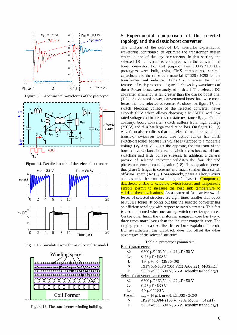
Figure 13 illustrates prototype behaviour at rated power. Input current Il(t) and switch voltage VS(t) are plotted on the same time graph. In general, these waveforms fit well the simulation ones. In particular, no overvoltage occurs when S switches off, confirming that the switching cell is well designed.
However parasitic ringing affects input current Il(t) during phase 2. Moreover, when phase 3 starts, the input current value Il(dTS
+) is smaller than expected. The previous model cannot anticipate these two ringing phenomena. In an attempt to better fit the transformer behaviour, we must indeed take its parasitic capacitor CPO into account (figure 14). In figure 14, RPO represents the ringing damping effect due to value magnetic core loss and wiring conduction loss. This new scheme allows predicting the detailed prototype behaviour. Impedance-meter analysis was conducted with a 4192A (5 Hz – 13 MHz) impedance analyser HP device. It confirms a magnetizing inductance Lm and leakage inductance Ll close to 44 µH and a 1 µH respectively. It also gives CPO about a hundred pF value. It also validates the ringing frequency of 2 MHz. RP0 resistance value is set to 10 kΩ after a fitting process while comparing experimental results and simulation ones. Figure 14 illustrates a rated power simulation with the following parameters values: CPO = 100 pF and RPO = 10 kΩ.
In brief, phase 3 is divided in two phases: phase 3-1 and phase 3-2. During phase 3-1, output diode DO does not yet conduct and for that reason the parasitic capacitor voltage can evolve freely. As Lm >> Ll, one can assume that Lm behaves as a current source Im. Similarly, CC >> CPO implies CC can be considered as a voltage source VC. Consequently, a resonant circuit takes place with Ll in the primary side and CPO in the secondary side. Phase 3-1 ends when diode DO switches on. At that specific time, the current drop ∆Il can be computed as:
Cl
POl V
LCmI =∆ (22)
This means that a part of the energy stored in the leakage inductor is not transferred to the non-dissipative clamp system but to the parasitic capacitor CPO. This energy is lost during the phase 2 when the same resonant circuit oscillates during several periods: energy dissipation occurs in windings and core material.
As a conclusion, these two parasitic ringing phenomena have a detrimental effect on the converter efficiency. According to equation (22), the smaller CPO value is, the more efficient the clamping system is. Hence the transformer design has to reduce the parasitic capacitance value. That is the reason why the primary and secondary inductors are winded with a winding spacer (figure 16).
8
1 Phase 2 4 3-2 3-1
∆Il
PFC = 100 W VFC = 25 W
Figure 13. Experimental waveforms of the prototype
VFC
VLoad
Electric Load
S CO
iS
DO
*
*
IFC CC DC
m
vC
Lm
Ll
IDc ICc
i2
Im
il
CI
mi2
CPO RPO
uS(t)
TS Figure 14. Detailed model of the selected converter
3.98 3.982 3.984 3.986 3.988 3.99 3.992 3.994 3.996 3.998 4
x 10-3
0
5
10
ik (A
)
3.98 3.982 3.984 3.986 3.988 3.99 3.992 3.994 3.996 3.998 4
x 10-3
0
20
40
60
temps (s)
vk (V
)
Time (µs)
vS (V)
iS (A)
0 10 20 2 4 6 8
0 10 20 2 4 6 8 0
VFC = 25 V PFC = 80 W
Figure 15. Simulated waveforms of complete model
Coil Former
Winding spacer
Figure 16. The transformer winding building
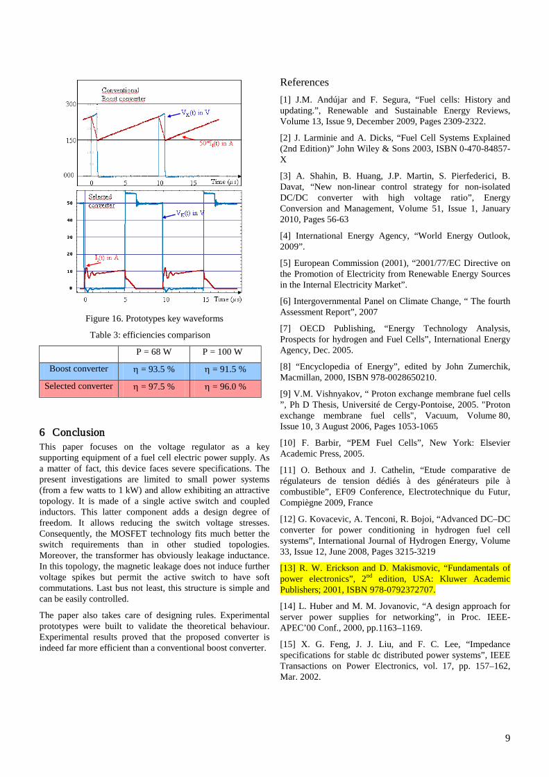
5 Exper imental compar ison of the selected topology and the classic boost conver ter The analysis of the selected DC converter experimental waveforms contributed to optimize the transformer design which is one of the key components. In this section, the selected DC converter is compared with the conventional boost converter. For that purpose, two 100 W / 100 kHz prototypes were built, using CMS components, ceramic capacitors and the same core material ETD39 / 3C90 for the transformer and inductor. Table 2 summarizes the main features of each prototype. Figure 17 shows key waveforms of them. Power losses were analysed in detail. The selected DC converter efficiency is far greater than the classic boost one. (Table 3). At rated power, conventional boost has twice more losses than the selected converter. As shown on figure 17, the switch blocking voltage of the selected converter never exceeds 60 V which allows choosing a MOSFET with low rated voltage and hence low on-state resistance RDSON. On the contrary, boost converter switch suffers from high voltage (250 V) and thus has large conduction loss. On figure 17, il(t) waveform also confirms that the selected structure avoids the transistor switch-on losses. The active switch has small switch-off losses because its voltage is clamped to a moderate voltage (VC ≅ 50 V). Quite the opposite, the transistor of the boost converter faces important switch losses because of hard switching and large voltage stresses. In addition, a general picture of selected converter validates the four depicted phases and corroborates equation (18). This equation proves that phase 3 length is constant and much smaller than switch off-state length (1-d)TS. Consequently, phase 4 always exists and assures the soft switching of phase 1. Components datasheets enable to calculate switch losses, and temperature sensors permit to measure the heat sink temperature to validate these evaluations. As a matter of fact, active switch losses of selected structure are eight times smaller than boost MOSFET losses. It points out that the selected converter has an efficient topology with respect to switch stresses. This fact is also confirmed when measuring switch cases temperatures. On the other hand, the transformer magnetic core has two to three times more losses than the inductor magnetic core. The ringing phenomena described in section 4 explain this result. But nevertheless, this drawback does not offset the other advantages of the selected structure.
Table 2: prototypes parameters
CI Boost parameters:
6800 µF / 63 V and 22 µF / 50 V CO 0.47 µF / 630 V L 150 µH, ETD39 / 3C90 S IXFV50N30PS (300 V/52 A/66 mΩ) MOSFET D SDD04S60 (600 V, 5.6 A, schottky technology)
CI Selected converter parameters:
6800 µF / 63 V and 22 µF / 50 V CO 0.47 µF / 630 V CC 4.7 µF / 100 V
Transf. Lm = 44 µH, m = 8, ETD39 / 3C90 S IRFS4610PbF (100 V, 73 A, RDSON = 14 mΩ) D SDD04S60 (600 V, 5.6 A, schottky technology)
9
Figure 16. Prototypes key waveforms
Table 3: efficiencies comparison
P = 68 W P = 100 W
Boost converter η = 93.5 % η = 91.5 %
Selected converter η = 97.5 % η = 96.0 %
6 Conclusion This paper focuses on the voltage regulator as a key supporting equipment of a fuel cell electric power supply. As a matter of fact, this device faces severe specifications. The present investigations are limited to small power systems (from a few watts to 1 kW) and allow exhibiting an attractive topology. It is made of a single active switch and coupled inductors. This latter component adds a design degree of freedom. It allows reducing the switch voltage stresses. Consequently, the MOSFET technology fits much better the switch requirements than in other studied topologies. Moreover, the transformer has obviously leakage inductance. In this topology, the magnetic leakage does not induce further voltage spikes but permit the active switch to have soft commutations. Last bus not least, this structure is simple and can be easily controlled.
The paper also takes care of designing rules. Experimental prototypes were built to validate the theoretical behaviour. Experimental results proved that the proposed converter is indeed far more efficient than a conventional boost converter.
References [1] J.M. Andújar and F. Segura, “Fuel cells: History and updating.”, Renewable and Sustainable Energy Reviews, Volume 13, Issue 9, December 2009, Pages 2309-2322.
[2] J. Larminie and A. Dicks, “Fuel Cell Systems Explained (2nd Edition)” John Wiley & Sons 2003, ISBN 0-470-84857-X
[3] A. Shahin, B. Huang, J.P. Martin, S. Pierfederici, B. Davat, “New non-linear control strategy for non-isolated DC/DC converter with high voltage ratio”, Energy Conversion and Management, Volume 51, Issue 1, January 2010, Pages 56-63
[4] International Energy Agency, “World Energy Outlook, 2009”.
[5] European Commission (2001), “2001/77/EC Directive on the Promotion of Electricity from Renewable Energy Sources in the Internal Electricity Market”.
[6] Intergovernmental Panel on Climate Change, “ The fourth Assessment Report”, 2007
[7] OECD Publishing, “Energy Technology Analysis, Prospects for hydrogen and Fuel Cells”, International Energy Agency, Dec. 2005.
[8] “Encyclopedia of Energy”, edited by John Zumerchik, Macmillan, 2000, ISBN 978-0028650210.
[9] V.M. Vishnyakov, “ Proton exchange membrane fuel cells ”, Ph D Thesis, Université de Cergy-Pontoise, 2005. "Proton exchange membrane fuel cells", Vacuum, Volume 80, Issue 10, 3 August 2006, Pages 1053-1065
[10] F. Barbir, “PEM Fuel Cells”, New York: Elsevier Academic Press, 2005.
[11] O. Bethoux and J. Cathelin, “Etude comparative de régulateurs de tension dédiés à des générateurs pile à combustible”, EF09 Conference, Electrotechnique du Futur, Compiègne 2009, France
[12] G. Kovacevic, A. Tenconi, R. Bojoi, “Advanced DC–DC converter for power conditioning in hydrogen fuel cell systems”, International Journal of Hydrogen Energy, Volume 33, Issue 12, June 2008, Pages 3215-3219
[13] R. W. Erickson and D. Makismovic, “Fundamentals of power electronics”, 2nd edition, USA: Kluwer Academic Publishers; 2001, ISBN 978-0792372707.
[14] L. Huber and M. M. Jovanovic, “A design approach for server power supplies for networking”, in Proc. IEEE-APEC’00 Conf., 2000, pp.1163–1169.
[15] X. G. Feng, J. J. Liu, and F. C. Lee, “Impedance specifications for stable dc distributed power systems”, IEEE Transactions on Power Electronics, vol. 17, pp. 157–162, Mar. 2002.
10
[16] D. Maksimovic, S. Cuk, “Switching converters with wide DC conversion range”, IEEE Transaction on Power Electronics, 1991;6(1):151–7.
[17] L. Barbosa, J.B. Vieira, L.C. de Freitas, M.S. Vilela, V.J. Farias, “A buck quadratic PWM soft-switching converter using a single active switch. IEEE Transactions on Power Electronics 1999; 14(3):445–53.
[18] V.M. Pacheco, A.J. Do Nascimento, V.J. Farias, J.B. Vieira, LC.. de Freitas, “A quadratic buck converter with lossless commutation”, IEEE Transactions on Industrial Electronics 2000; 47(2):264–72.
[19] N. Mohan, T. M. Undeland, and W. P. Robbins, “Power Electronics”, John Wiley & Sons, 2002, 3rd Edition.
[20] L. Salazar; P.D. Ziogas, “A high frequency forward DC/DC converter topology with transformer flux balancing capability”, Industry Applications Society Annual Meeting, 1988., Conference Record of the 1988 IEEE 2-7 Oct. 1988 Page(s):785 - 792 vol.1
[21] K. W. Ma and Y. S. Lee, “An integrated flyback converter for dc uninterruptible power supply”, IEEE Transaction on. Power Electronics, vol. 11, pp.318–327, March 1996.
[22] Q. Zhao, F.C. Lee, “High-efficiency, high step-up DC-DC converters”, IEEE Transactions on Power Electronics, Volume 18, Issue 1, Part 1, Jan. 2003 Page(s):65 – 73
[23] Muhammad H. Rashid, “Power Electronics Handbook”, 2nd edition, Elsevier Academic Press, 2007, ISBN 978-0-12-088479-7.
[24] S. Lefebvre and F. Miserey, « Composants à semi-conducteur pour l’électronique de puissance », Lavoisier, (2004).
[25] N. Piette, E. Clavel and Y. Marechal, « Optimization of cabling in power electronics structure using inductance criterion », Industry Applications Conference, oct. 1998. Thirty-Third IAS Annual Meeting, vol.2, pp: 925 - 928.
[26] E. Clavel, Y. Marechal and J. Roudet « Modélisation des câblages en électronique de puissance: apport et complémentarité des methods d’éléments finis et de circuits équivalents », The European Physical Journal Applied Physics, EPJAP 1, pp: 211 – 223, 1998.
[27] J-L. Schanen, C. Guérin, J. Roudet, and Gérard Meunier, “Influence of a conductive plane on loop inductance”, IEEE Transactions on magnetic, vol. 31 n°3, may 1995.
[28] M. Zahn, « Electromagnetic field theory: a problem solving approach », John Wiley, 1979.
Related Documents