Design Notes of Microprocessor μ311.1 LECTURE NOTES - CENG311 COMPUTER ARCHITECTURE Tolga Ayav [email protected] December 19, 2017 Technical Report Department of Computer Engineering ˙ Izmir Institute of Technology 35430 Urla ˙ Izmir, Turkey. Web: http://compeng.iyte.edu.tr Technical Report No: IYTE-COMPENG-2017-001 ISSN: http://arf.iyte.edu.tr/pubs/2017/compeng-2017-001.pdf All rights, including translation into other languages are reserved by the authors. No part of this report may be reproduced or used in any form or by any means - graphically or mechanically, including photocopying, recording, taping or information and retrieval systems - without written permission from the authors.

Welcome message from author
This document is posted to help you gain knowledge. Please leave a comment to let me know what you think about it! Share it to your friends and learn new things together.
Transcript
Design Notes of Microprocessor µ311.1
LECTURE NOTES - CENG311 COMPUTER ARCHITECTURE
Tolga [email protected]
December 19, 2017
Technical ReportDepartment of Computer Engineering
Izmir Institute of Technology
35430 Urla Izmir, Turkey. Web: http://compeng.iyte.edu.tr
Technical Report No: IYTE-COMPENG-2017-001ISSN:http://arf.iyte.edu.tr/pubs/2017/compeng-2017-001.pdf
All rights, including translation into other languages are reserved by the authors. No part of this report may bereproduced or used in any form or by any means - graphically or mechanically, including photocopying, recording, tapingor information and retrieval systems - without written permission from the authors.

Technical Report No: IYTE-COMPENG-2017-001
Contents
1 External Parts 31.1 Reset Circuit . . . . . . . . . . . . . . . . . . . . . . . . . . . . . . . . . . . . . . . . . . . 31.2 Clock Circuit . . . . . . . . . . . . . . . . . . . . . . . . . . . . . . . . . . . . . . . . . . . 31.3 1024x16-bit ROM . . . . . . . . . . . . . . . . . . . . . . . . . . . . . . . . . . . . . . . . . 41.4 1024x16-bit RAM . . . . . . . . . . . . . . . . . . . . . . . . . . . . . . . . . . . . . . . . . 6
2 Microprocessor µ311.1 72.1 Instruction Set . . . . . . . . . . . . . . . . . . . . . . . . . . . . . . . . . . . . . . . . . . 82.2 Datapath . . . . . . . . . . . . . . . . . . . . . . . . . . . . . . . . . . . . . . . . . . . . . 15
2.2.1 Registers . . . . . . . . . . . . . . . . . . . . . . . . . . . . . . . . . . . . . . . . . 162.2.2 Program Counter . . . . . . . . . . . . . . . . . . . . . . . . . . . . . . . . . . . . . 162.2.3 Instruction Register, Stack Pointer . . . . . . . . . . . . . . . . . . . . . . . . . . . 182.2.4 Register File . . . . . . . . . . . . . . . . . . . . . . . . . . . . . . . . . . . . . . . 182.2.5 Multiplexers . . . . . . . . . . . . . . . . . . . . . . . . . . . . . . . . . . . . . . . 202.2.6 Buffers . . . . . . . . . . . . . . . . . . . . . . . . . . . . . . . . . . . . . . . . . . . 212.2.7 ALU and Shifter . . . . . . . . . . . . . . . . . . . . . . . . . . . . . . . . . . . . . 222.2.8 The processor . . . . . . . . . . . . . . . . . . . . . . . . . . . . . . . . . . . . . . . 32
2.3 Stack . . . . . . . . . . . . . . . . . . . . . . . . . . . . . . . . . . . . . . . . . . . . . . . . 332.4 Control Unit . . . . . . . . . . . . . . . . . . . . . . . . . . . . . . . . . . . . . . . . . . . 33
2.4.1 Bus Cycles . . . . . . . . . . . . . . . . . . . . . . . . . . . . . . . . . . . . . . . . 35
3 Testbench 63
4 Address Decoding and I/O Communication 64
5 Interrupts 65
6 Additional Instructions and Units 666.1 Watchdog Timer . . . . . . . . . . . . . . . . . . . . . . . . . . . . . . . . . . . . . . . . . 666.2 Base Pointer Register . . . . . . . . . . . . . . . . . . . . . . . . . . . . . . . . . . . . . . 66
7 Programming 687.1 High-Level Programming . . . . . . . . . . . . . . . . . . . . . . . . . . . . . . . . . . . . 687.2 Assembly and Linking . . . . . . . . . . . . . . . . . . . . . . . . . . . . . . . . . . . . . . 697.3 Sample Programs . . . . . . . . . . . . . . . . . . . . . . . . . . . . . . . . . . . . . . . . . 707.4 Assemblers . . . . . . . . . . . . . . . . . . . . . . . . . . . . . . . . . . . . . . . . . . . . 717.5 Linking . . . . . . . . . . . . . . . . . . . . . . . . . . . . . . . . . . . . . . . . . . . . . . 72
8 Instruction Pipelining 79
A Simulation in ModelSim PE Student Edition 83
B BNF Syntax for VHDL 84
C Implementation Hierarchy 92
Tolga Ayav 1 / 100

D as311 Assembler 93
E Multitasking in µ311.1 96E.1 16-bit timer . . . . . . . . . . . . . . . . . . . . . . . . . . . . . . . . . . . . . . . . . . . . 96
F µ311.1 Internal Schematic 99

Technical Report No: IYTE-COMPENG-2017-001
Design Notes of Microprocessor µ311.1
Lecture Notes of CENG311 Computer Architecture
Tolga Ayav
December 19, 2017
Preface
This handbook includes a part of the lecture notes of CENG 311 Computer Architecture course given inthe undergraduate program of the Department of Computer Engineering at Izmir Institute of Technology.
One aim of this course is to introduce the preliminaries of a general purpose microprocessor design.To this end, I aim to teach a very simple microprocessor which we call µ311.1 , an 16-bit processor withonly 25 instructions.
This document is intended to help the students with their laboratory works. In the experimentalpart of the course, students are expected to implement this or another similar processor using VHDL inorder to attain a sufficient knowledge and intuition about “What is really happening inside a computersystem?”.
In other words, starting from typing printf("value:%d",*p); they must understand compiling,assembling, linking, loading the machine code and how processors execute this code. This document aimsto give a very short and abstract answer to the above question.
Students may find many parts missing, too short or incomplete. Nonetheless, I hope that this will bea good starting point for their deeper research as well as their study of computer architecture.
Tolga Ayav 1 / 100

Technical Report No: IYTE-COMPENG-2017-001
Figure 1: µ311.1 internal diagramTolga Ayav 2 / 100

Technical Report No: IYTE-COMPENG-2017-001
1 External Parts
1.1 Reset Circuit
µ311.1 needs an external reset circuit as given in Figure 2. The reset signal is used to restart themicroprocessor properly. Depending on the design, for a proper reset, this signal must be given to theprocessor for a certain period of time.
Figure 2: Reset circuit.
1 -- reset.vhd: Reset circuit
2
3 library IEEE;
4 use IEEE.STD_LOGIC_1164.ALL;
5 use IEEE.STD_LOGIC_ARITH.ALL;
6 use IEEE.STD_LOGIC_UNSIGNED.ALL;
7
8 entity rst_gen is port (reset : out std_logic);
9 end rst_gen;
10
11 architecture Behavioral of rst_gen is
12
13 constant rst_period : time := 100 us;
14
15 reset <= ’1’ after 0 us, ’0’ after rst_period;
16
17 end Behavioral;
1.2 Clock Circuit
1 -- clock.vhd: Clock signal generator
2
3 library IEEE;
4 use IEEE.STD_LOGIC_1164.ALL;
5 use IEEE.STD_LOGIC_ARITH.ALL;
6 use IEEE.STD_LOGIC_UNSIGNED.ALL;
Tolga Ayav 3 / 100

Technical Report No: IYTE-COMPENG-2017-001
Figure 3: Clock generator using digital inverter. For C1 = 1nF and R1 = 1kΩ, f = 1MHz.
7
8 entity clk_gen is port (clk : out std_logic);
9 end clk_gen;
10
11 architecture Behavioral of clk_gen is
12 constant clk_period : time := 1 us;
13 clk_process :process
14 begin
15 clk <= ’0’;
16 wait for clk_period/2; --for 0.5 us signal is ’0’.
17 clk <= ’1’;
18 wait for clk_period/2; --for next 0.5 us signal is ’1’.
19 end process;
20 end Behavioral;
Question 1 Discuss about “Synthesizable VHDL code”. Are “clock.vhd” and “reset.vhd” synthesizablecodes?
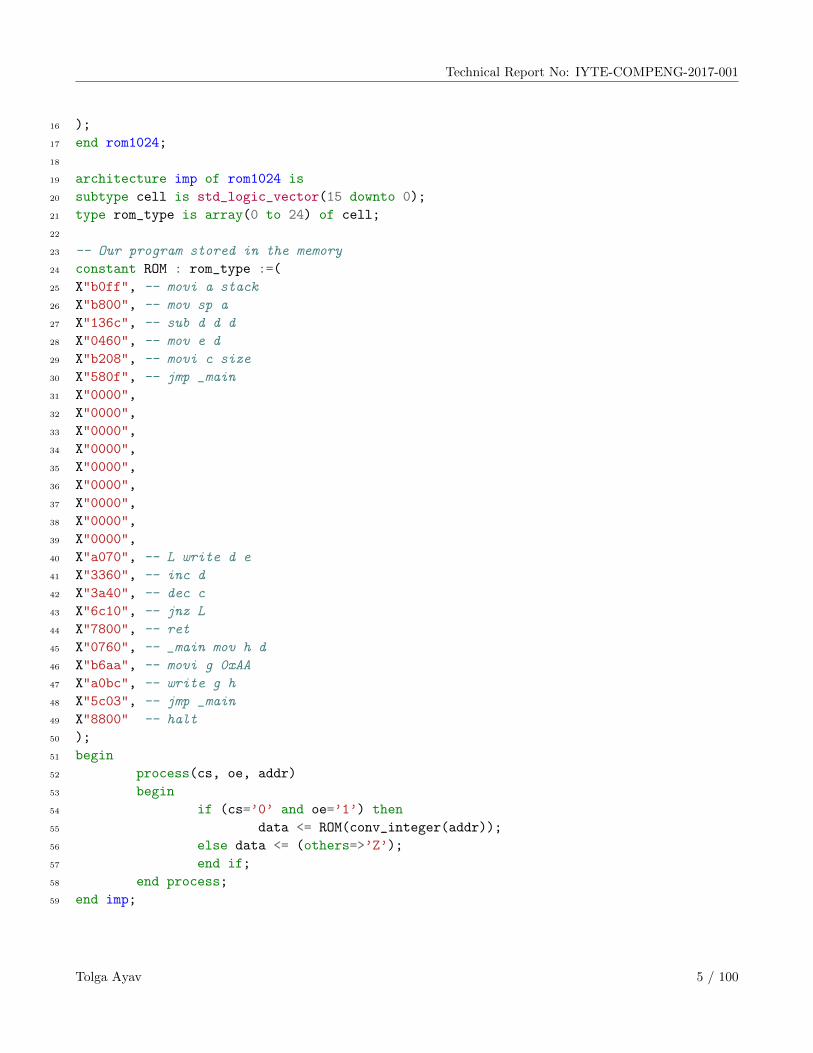
1.3 1024x16-bit ROM
1 -- rom1024.vhd: 1024x16bit ROM
2
3 library ieee;
4 library work;
5 use ieee.std_logic_1164.all;
6 use ieee.std_logic_unsigned.all;
7 use ieee.numeric_std.all;
8 use work.u311.all;
9 use work.opcodes.all;
10
11 entity rom1024 is port(
12 cs : in std_logic;
13 oe : in std_logic;
14 addr : in std_logic_vector (9 downto 0);
15 data : out std_logic_vector (15 downto 0)
Tolga Ayav 4 / 100
Technical Report No: IYTE-COMPENG-2017-001
16 );
17 end rom1024;
18
19 architecture imp of rom1024 is
20 subtype cell is std_logic_vector(15 downto 0);
21 type rom_type is array(0 to 24) of cell;
22
23 -- Our program stored in the memory
24 constant ROM : rom_type :=(
25 X"b0ff", -- movi a stack
26 X"b800", -- mov sp a
27 X"136c", -- sub d d d
28 X"0460", -- mov e d
29 X"b208", -- movi c size
30 X"580f", -- jmp _main
31 X"0000",
32 X"0000",
33 X"0000",
34 X"0000",
35 X"0000",
36 X"0000",
37 X"0000",
38 X"0000",
39 X"0000",
40 X"a070", -- L write d e
41 X"3360", -- inc d
42 X"3a40", -- dec c
43 X"6c10", -- jnz L
44 X"7800", -- ret
45 X"0760", -- _main mov h d
46 X"b6aa", -- movi g 0xAA
47 X"a0bc", -- write g h
48 X"5c03", -- jmp _main
49 X"8800" -- halt
50 );
51 begin
52 process(cs, oe, addr)
53 begin
54 if (cs=’0’ and oe=’1’) then
55 data <= ROM(conv_integer(addr));
56 else data <= (others=>’Z’);
57 end if;
58 end process;
59 end imp;
Tolga Ayav 5 / 100

Technical Report No: IYTE-COMPENG-2017-001
We have an assembler, namely as311, to translate the assembly programs to the machine code ofµ311.1 . The assembler generates a special output file with .vhdl hex extension. It can be copied andpasted to the appropriate place in the rom1024.vhd.
1.4 1024x16-bit RAM
Stack operations require a volatile memory. An implementation of 1024x16 bit RAM is as follows:
1 library ieee;
2 use ieee.std_logic_1164.all;
3 use ieee.std_logic_unsigned.all;
4 use ieee.numeric_std.all;
5
6 entity ram1024 is port(
7 rst: in std_logic;
8 cs: in std_logic; --chip select
9 wr: in std_logic; --write enable
10 rd: in std_logic;--read enable
11 addr: in std_logic_vector(9 downto 0);
12 data: inout std_logic_vector(15 downto 0));
13 end ram1024;
14
15 architecture imp of ram1024 is
16 subtype cell is std_logic_vector(15 downto 0);
17 type ram_type is array(0 to 1023) of cell;
18 signal RAM: ram_type;
19
20 begin
21
22 process(cs,wr,rd,addr)
23 begin
24 if ( cs=’0’ and rd=’1’) then
25 data <= RAM(conv_integer(addr));
26 elsif( cs=’0’ and wr=’1’) then
27 RAM(conv_integer(addr)) <= data after 10ns ;
28 else data <= (others=>’Z’);
29 end if;
30 end process;
31
32 end imp;
Tolga Ayav 6 / 100

Technical Report No: IYTE-COMPENG-2017-001
2 Microprocessor µ311.1
The general specifications of µ311.1 are:
• 16-bit processor
• 39 pins
• Addresses up to 64k locations
• No internal program memory
• 8x16-bit general purpose registers
• interrupt mechanism (supports 8 external interrupts)
• 4 cycles: opcode fetch, read memory-I/O, write memory-I/O and interrupt cycles.
• 25 single-word instructions with single cycle operation.
Figure 4 shows a general diagram of µ311.1 . µ311.1 is a simple 16-bit processor. It has the following
Figure 4: µ311.1 pinout
inputs/outputs:
clk is clock signal that is needed by the microprocessor.
reset restarts the microprocessor.
int is the hardware interrupt signal that is used for event triggering.
inta is the acknowledge of µ311.1 as a response to the interrupt request of an external device.
address bus is an 16-bit bus that is used for the communication with external memory and I/O devices.It can address up to 64k locations.
data bus is an 16-bit bus that is used for the data transfer between external devices and µ311.1 .
Tolga Ayav 7 / 100

Technical Report No: IYTE-COMPENG-2017-001
wr indicates a write cycle.
rd indicates a read cycle.
opfetch indicates an opcode fetch cycle.
All control signals of µ311.1 (wr,rd,reset,int,inta,opfetch) are active high. This means that wr=1 indicatesa write cycle and the microprocessor is reset when reset=1.
Figure 5: The two 64k memory maps of µ311.1 .
Question 2 Write a simulator in Java for µ311.1 . Your simulator should take an assembly programas input and execute it. During the simulation, registers and other critical values will be shown on thescreen.
2.1 Instruction Set
µ311.1 ’s limited instruction set has only 25 instructions. These commands are given in Table 1. Toencode 25 instructions, the operation code (opcode) requires 5 bits, giving us 32 different combinations.As shown in the encoding column, the five most significant bits represent the opcode of the instructions.For example, the opcode for mov is 00000 and the opcode for movi is 10111 and so on.
Tolga Ayav 8 / 100

Technical Report No: IYTE-COMPENG-2017-001
Table 1: Instruction set of µ311.1 . Each instruction is 16-bit long.
Opcode Instruction Encoding Operation Comment
00000 mov R1, R2 00000 r1r1r1 r2r2r2 x x x uu R1 ← R2 move register00001 add R1, R2, R3 00001 r1r1r1 r2r2r2 r3r3r3 uu R1 ← R2 + R3 addition00010 sub R1, R2, R3 00010 r1r1r1 r2r2r2 r3r3r3 uu R1 ← R2 - R3 subtraction00011 and R1, R2, R3 00011 r1r1r1 r2r2r2 r3r3r3 uu R1 ← R2 & R3 logical and00100 or R1, R2, R3 00100 r1r1r1 r2r2r2 r3r3r3 uu R1 ← R2 | R3 logical or00101 not R 00101 rrr rrr xxx uu R ← not R logical not00110 inc R 00110 rrr rrr xxx uu R ← R+1 increment00111 dec R 00111 rrr rrr xxx uu R ← R-1 decrement01000 sr R 01000 rrr rrr xxx uu R ← R >> 1 shift right01001 sl R 01001 rrr rrr xxx uu R ← R << 1 shift left01010 rr R 01010 rrr rrr xxx uu R15 ← R0; shift right
R ← R >> 101011 jmp add11 01011 aaaaaaaaaaa PC ← PC+add11 jump01100 jz add11 01100 aaaaaaaaaaa if(zero) jump if zero
PC ← PC+add1101101 jnz add11 01101 aaaaaaaaaaa if(!zero) jump if not zero
PC ← PC+add1101110 call add11 01110 aaaaaaaaaaa push PC; call function
PC ← PC+add1101111 ret 01111 uuuuuuuuuuu SP← SP+1; return
PC ← mem[SP]10000 nop 10000 uuuuuuuuuuu - no operation10001 halt 10001 uuuuuuuuuuu - halt processor10010 push R 10010 xxx xxx rrr uu mem[SP] ← R; push R onto stack
SP ← SP-110011 pop R 10011 rrr xxx xxx uu SP ← SP+1; pop R from stack
R ← mem[SP]10100 write @R1, R2 10100 x x x r1r1r1 r2r2r2 uu mem[R1] ← R2 write to memory10101 read R1, @R2 10101 r1r1r1 r2r2r2 x x x uu R1 ← mem[R2] read from memory10110 movi R, imm8 10110 rrr iiiiiiii R ← imm8 move immediate10111 mov SP, R 10111 xxx rrr xxx uu SP ← R move to SP11000 mov R, SP 11000 rrr xxx xxx uu R ← SP move from SP11001110101101111100111011111011111
r, r1, r2 = 16-bit register mem[65536] = 64 kW memoryadd11 = 11-bit signed integer imm8 = 8-bit immediate value
PC = program counter register SP = stack pointer registerzero = zero flag x, u = “don’t care”and undefined bits.
Tolga Ayav 9 / 100

Technical Report No: IYTE-COMPENG-2017-001
mov R1, R2
Meaning: R1=R2
This command copies the content of register R2 to register R1. Note that this is not a move operationsince the source register is not altered. An example command and its equivalent machine codes is:mov H, A (00000 111 000 000 00)
add R1, R2, R3
Meaning: R1=R2+R3
This command calculates the sum of R2 and R3. The result is then placed into R1. An example commandand its equivalent machine codes is:add A, B, C (00001 000 001 010 00)
sub R1, R2, R3
Meaning: R1=R2-R3
This command subtracts R3 from R2. The result is then placed into R1. An example command and itsequivalent machine codes is:sub A, B, C (00010 000 001 010 00)
and R1, R2, R3
Meaning: R1=R2 and R3
Tolga Ayav 10 / 100

Technical Report No: IYTE-COMPENG-2017-001
This is logical and operation. An example command and its equivalent machine codes is:and A, B, C (00011 000 001 010 00)
or R1, R2, R3
Meaning: R1=R2 or R3
This is logical and operation. An example command and its equivalent machine codes is:or A, B, C (00100 000 001 010 00)
not R
Meaning: R=not R
This command provides negation operation. An example command and its equivalent machine codes is:not B (00101 001 001 000 00)
inc R
Meaning: R++
This command increments the content of a register by 1. An example command and its equivalent ma-chine codes is:inc c (00110 010 010 000 00)
dec R
Meaning: R−−
This command decrements the content of a register by 1. An example command and its equivalent ma-chine codes is:dec c (00111 010 010 000 00)
Tolga Ayav 11 / 100

Technical Report No: IYTE-COMPENG-2017-001
sr R
Meaning: R>> 1
Shift right operation shifts the given register to the right. Same as dividing by 2. The rightmost bit isdiscarded. An example command and its equivalent machine codes is:sr c (01000 010 010 000 00)
sl R
Meaning: R<< 1
Shift left operation shifts the given register to the left. Same as multiplying by 2. The leftmost bit isdiscarded. An example command and its equivalent machine codes is:sl c (01001 010 010 000 00)
rr R
Meaning: t=R.0; R>> 1; R.15=t;
Rotate right operation shifts the given register to the right. The rightmost bit is moved to the leftmostbit. An example command and its equivalent machine codes is:rr c (01010 010 010 000 00)
jmp add11
Meaning: PC=PC ± add11
This jumps the execution to another location. The address of the new location will be PC ± add11 (add11is a signed integer) An example command and its equivalent machine codes is:jmp 03H (01100 00000000011)
jz add11
Meaning: if(zero) PC=PC ± add11
Tolga Ayav 12 / 100

Technical Report No: IYTE-COMPENG-2017-001
This jumps the execution to another location if zero flag is set. The address of the new location will bePC ± add11 (add11 is a signed integer) An example command and its equivalent machine codes is:jz 03H (01101 00000000011)
jnz add11
Meaning: if(!zero) PC=PC ± add11
This jumps the execution to another location if zero flag is not set. The address of the new location willbe PC ± add11 (add11 is a signed integer) An example command and its equivalent machine codes is:jnz 03H (01110 00000000011)
call add11
Meaning: push PC; PC=PC ± add11
This command calls a procedure. The starting address is PC ± add11. It is similar to jmp command.The only difference is that the return address is pushed onto the stack a priori. An example commandand its equivalent machine codes is:call 03H (01111 00000000011)
ret
Meaning: pop PC ≡ PC=mem[SP++]
This command returns from procedure. The memory address that will be returned to is popped from thestack. An example command and its equivalent machine codes is:ret (10000 00000000000)
nop
Meaning: -
This is no operation (Discuss: When do we need this command?).
Tolga Ayav 13 / 100

Technical Report No: IYTE-COMPENG-2017-001
nop (10001 00000000000)
halt
Meaning: Halting
This command halts the processor. In other words, execution is stopped (Discuss: When can we needthis command? Why?). An example command and its equivalent machine codes is:halt (10010 00000000000)
push R
Meaning: mem[SP]=R; SP–;
Pushes register R onto the stack memory. An example command and its equivalent machine codes is:push B (10010 000 000 001 00)
pop R
Meaning: SP++; R=mem[SP]
Popes register R from the stack memory. An example command and its equivalent machine codes is:pop B (10100 001 000 000 00)
write @R1, R2
Meaning: mem[R1]=R2
Writes the content of R2 into the memory location that is is pointed by R1. An example command andits equivalent machine codes is:write @D, B (10101 000 011 001 00)
read R1, @R2
Meaning: R1=mem[R2]
Tolga Ayav 14 / 100

Technical Report No: IYTE-COMPENG-2017-001
Reads from memory. An example command and its equivalent machine codes is:read B, @D (10101 001 011 000 00)
movi R, imm8
Meaning:
Places 8-bit immediate value imm8 into R’s less significant 8-bit portion. An example command and itsequivalent machine codes is:movi B, 05H (10111 001 00000101)
mov SP, R
Meaning:
Copies register R to SP. An example command and its equivalent machine codes is:mov SP, B (10111 000 001 000 00)
mov R, SP
Meaning:
Copies SP to register R. An example command and its equivalent machine codes is:mov B, SP (11000 001 000 000 00)
2.2 Datapath
The datapath is responsible for manipulating data. It includes (1) functional units such as adders, shifters,multipliers, ALUs, and comparators, (2) registers and other memory elements for the temporary storageof data, and (3) buses, multiplexers, and tri-state buffers for the transfer of data between the differentcomponents in the datapath, and the external world. External data enters the datapath through the datainput lines. Results from the datapath operations are provided through the data output lines. Thesesignals serve as the primary input/output data ports for the microprocessor. In the following subsections,we will see the components of the datapath in detail.
Tolga Ayav 15 / 100

Technical Report No: IYTE-COMPENG-2017-001
2.2.1 Registers
µ311.1 has 8 general purpose registers and three special purpose registers that are program counter (PC),instruction register (IR) and stack pointer (SP). The following VHDL code is the description of a generic16-bit register.
1 library ieee;
2 use ieee.std_logic_1164.all;
3 use ieee.std_logic_unsigned.all;
4 use ieee.numeric_std.all;
5
6 library work;
7 use work.uP.all;
8
9 entity reg16 is port(
10 d: in std_logic_vector(15 downto 0);
11 ld: in std_logic; --load/enable.
12 clr: in std_logic; --async clear.
13 clk: in std_logic; --clock.
14 q: out std_logic_vector(15 downto 0) --output.
15 );
16 end reg16;
17
18 architecture description of reg16 is
19
20 begin
21 process(clk, clr)
22 begin
23 if clr = ’1’ then
24 q <= x"0000";
25 elsif rising_edge(clk) then
26 if ld = ’1’ then
27 q <= d;
28 end if;
29 end if;
30 end process;
31 end description;
In the architecture body of µ311.1 implementation, special purpose registers can be implementedusing register16.
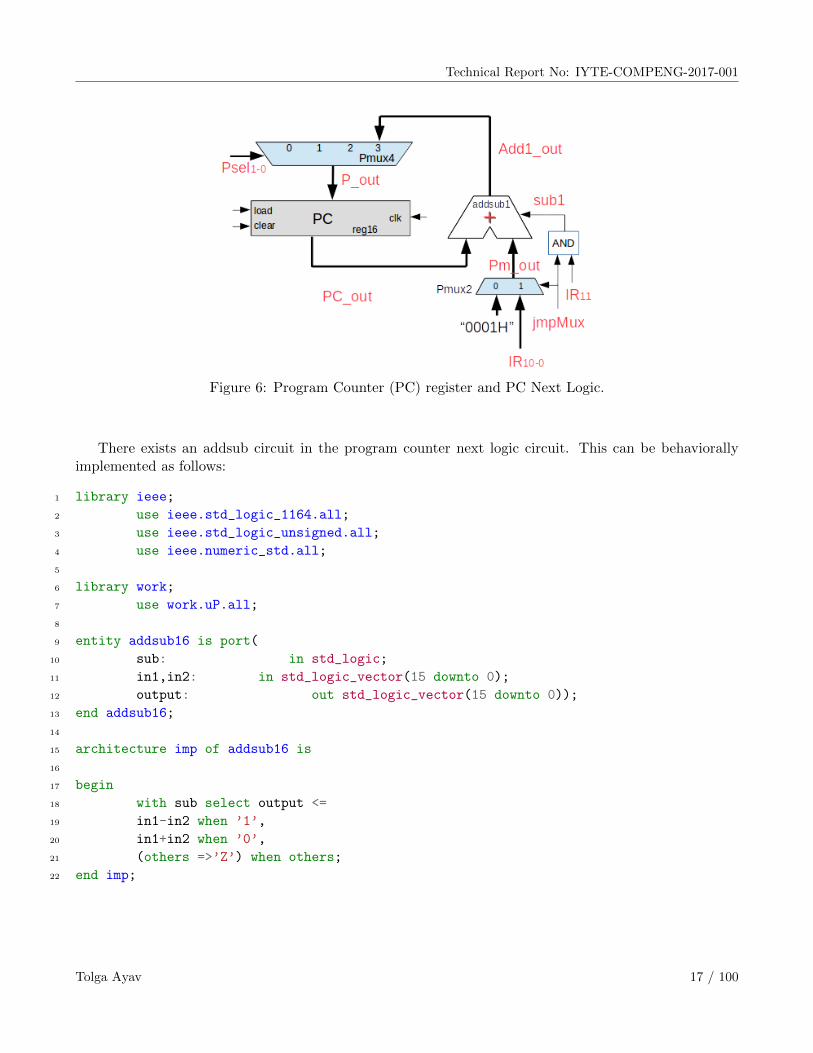
2.2.2 Program Counter
Program counter (PC) contains the memory location of where the next instruction is stored. Eachtime an instruction is fetched from a memory location pointed to by the PC, normally the PC must beincremented to the next memory location for the next instruction. Alternatively, if the instruction is ajump instruction, the PC must be loaded with a new memory address instead.
Tolga Ayav 16 / 100
Technical Report No: IYTE-COMPENG-2017-001
Figure 6: Program Counter (PC) register and PC Next Logic.
There exists an addsub circuit in the program counter next logic circuit. This can be behaviorallyimplemented as follows:
1 library ieee;
2 use ieee.std_logic_1164.all;
3 use ieee.std_logic_unsigned.all;
4 use ieee.numeric_std.all;
5
6 library work;
7 use work.uP.all;
8
9 entity addsub16 is port(
10 sub: in std_logic;
11 in1,in2: in std_logic_vector(15 downto 0);
12 output: out std_logic_vector(15 downto 0));
13 end addsub16;
14
15 architecture imp of addsub16 is
16
17 begin
18 with sub select output <=
19 in1-in2 when ’1’,
20 in1+in2 when ’0’,
21 (others =>’Z’) when others;
22 end imp;
Tolga Ayav 17 / 100

Technical Report No: IYTE-COMPENG-2017-001
2.2.3 Instruction Register, Stack Pointer
Instruction register (IR) stores the instruction being fetched from the program memory. PC, IR and SPcan be implemented in the datapath using the 16-bit register as seen below:
1 PCx: reg16 port map(P_out,PCload,reset,clk,PC_out);
2 IRx: reg16 port map(RB,IRload,reset,clk,IR_out);
3 SPx: reg16 port map(S_out,SPload,reset,clk,SP_out);
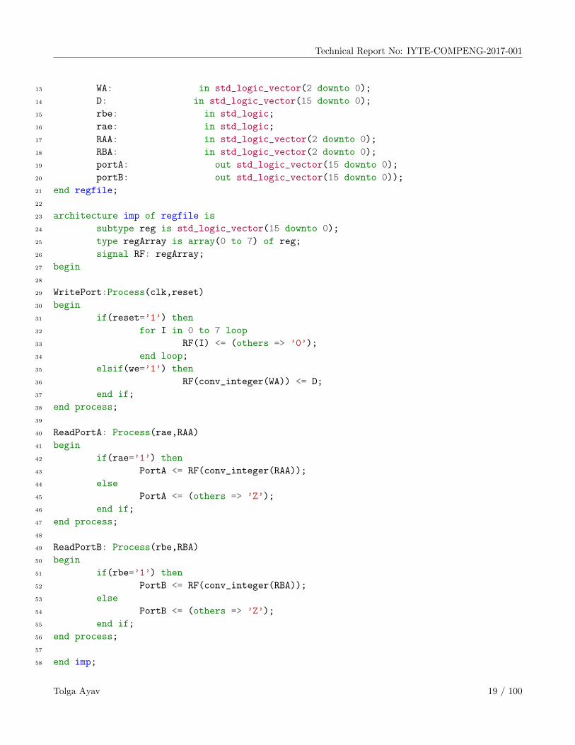
2.2.4 Register File
Register file contains 32 registers. The block diagram of the register file is seen in Figure 7.
Figure 7: ALU and register file
1 library ieee;
2 use ieee.std_logic_1164.all;
3 use ieee.std_logic_unsigned.all;
4 use ieee.numeric_std.all;
5
6 library work;
7 use work.uP.all;
8
9 entity regfile is port(
10 clk: in std_logic;
11 reset: in std_logic;
12 we: in std_logic;
Tolga Ayav 18 / 100
Technical Report No: IYTE-COMPENG-2017-001
13 WA: in std_logic_vector(2 downto 0);
14 D: in std_logic_vector(15 downto 0);
15 rbe: in std_logic;
16 rae: in std_logic;
17 RAA: in std_logic_vector(2 downto 0);
18 RBA: in std_logic_vector(2 downto 0);
19 portA: out std_logic_vector(15 downto 0);
20 portB: out std_logic_vector(15 downto 0));
21 end regfile;
22
23 architecture imp of regfile is
24 subtype reg is std_logic_vector(15 downto 0);
25 type regArray is array(0 to 7) of reg;
26 signal RF: regArray;
27 begin
28
29 WritePort:Process(clk,reset)
30 begin
31 if(reset=’1’) then
32 for I in 0 to 7 loop
33 RF(I) <= (others => ’0’);
34 end loop;
35 elsif(we=’1’) then
36 RF(conv_integer(WA)) <= D;
37 end if;
38 end process;
39
40 ReadPortA: Process(rae,RAA)
41 begin
42 if(rae=’1’) then
43 PortA <= RF(conv_integer(RAA));
44 else
45 PortA <= (others => ’Z’);
46 end if;
47 end process;
48
49 ReadPortB: Process(rbe,RBA)
50 begin
51 if(rbe=’1’) then
52 PortB <= RF(conv_integer(RBA));
53 else
54 PortB <= (others => ’Z’);
55 end if;
56 end process;
57
58 end imp;
Tolga Ayav 19 / 100
Technical Report No: IYTE-COMPENG-2017-001
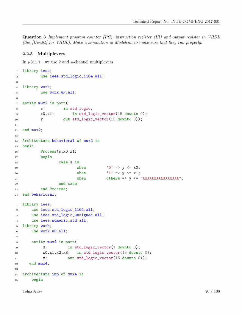
Question 3 Implement program counter (PC), instruction register (IR) and output register in VHDL(See [Hwa04] for VHDL). Make a simulation in Modelsim to make sure that they run properly.
2.2.5 Multiplexers
In µ311.1 , we use 2 and 4-channel multiplexers.
1 library ieee;
2 use ieee.std_logic_1164.all;
3
4 library work;
5 use work.uP.all;
6
7 entity mux2 is port(
8 s: in std_logic;
9 x0,x1: in std_logic_vector(15 downto 0);
10 y: out std_logic_vector(15 downto 0));
11
12 end mux2;
13
14 Architecture behavioral of mux2 is
15 begin
16 Process(s,x0,x1)
17 begin
18 case s is
19 when ’0’ => y <= x0;
20 when ’1’ => y <= x1;
21 when others => y <= "XXXXXXXXXXXXXXXX";
22 end case;
23 end Process;
24 end behavioral;
1 library ieee;
2 use ieee.std_logic_1164.all;
3 use ieee.std_logic_unsigned.all;
4 use ieee.numeric_std.all;
5 library work;
6 use work.uP.all;
7
8 entity mux4 is port(
9 S: in std_logic_vector(1 downto 0);
10 x0,x1,x2,x3: in std_logic_vector(15 downto 0);
11 y: out std_logic_vector(15 downto 0));
12 end mux4;
13
14 architecture imp of mux4 is
15 begin
Tolga Ayav 20 / 100
Technical Report No: IYTE-COMPENG-2017-001
16 process(S, x0, x1, x2, x3)
17 begin
18 case S is
19 when "00" => y <= x0;
20 when "01" => y <= x1;
21 when "10" => y <= x2;
22 when "11" => y <= x3;
23 when others => y <= "XXXXXXXXXXXXXXXX";
24 end case;
25 end process;
26 end imp;
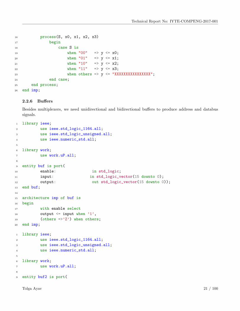
2.2.6 Buffers
Besides multiplexers, we need unidirectional and bidirectional buffers to produce address and databussignals.
1 library ieee;
2 use ieee.std_logic_1164.all;
3 use ieee.std_logic_unsigned.all;
4 use ieee.numeric_std.all;
5
6 library work;
7 use work.uP.all;
8
9 entity buf is port(
10 enable: in std_logic;
11 input: in std_logic_vector(15 downto 0);
12 output: out std_logic_vector(15 downto 0));
13 end buf;
14
15 architecture imp of buf is
16 begin
17 with enable select
18 output <= input when ’1’,
19 (others =>’Z’) when others;
20 end imp;
1 library ieee;
2 use ieee.std_logic_1164.all;
3 use ieee.std_logic_unsigned.all;
4 use ieee.numeric_std.all;
5
6 library work;
7 use work.uP.all;
8
9 entity buf2 is port(
Tolga Ayav 21 / 100
Technical Report No: IYTE-COMPENG-2017-001
10 enable: in std_logic;
11 direction: in std_logic;
12 input: inout std_logic_vector(15 downto 0);
13 output: inout std_logic_vector(15 downto 0));
14 end buf2;
15
16 architecture imp of buf2 is
17 begin
18 Bproc: process(enable,direction,input,output)
19 begin
20 if(enable=’1’ and direction=’1’) then output <= input;
21 elsif(enable=’1’ and direction=’0’) then input <= output;
22 else input <= (others => ’Z’);
23 output <= (others =>’Z’);
24 end if;
25 end process;
26 end imp;
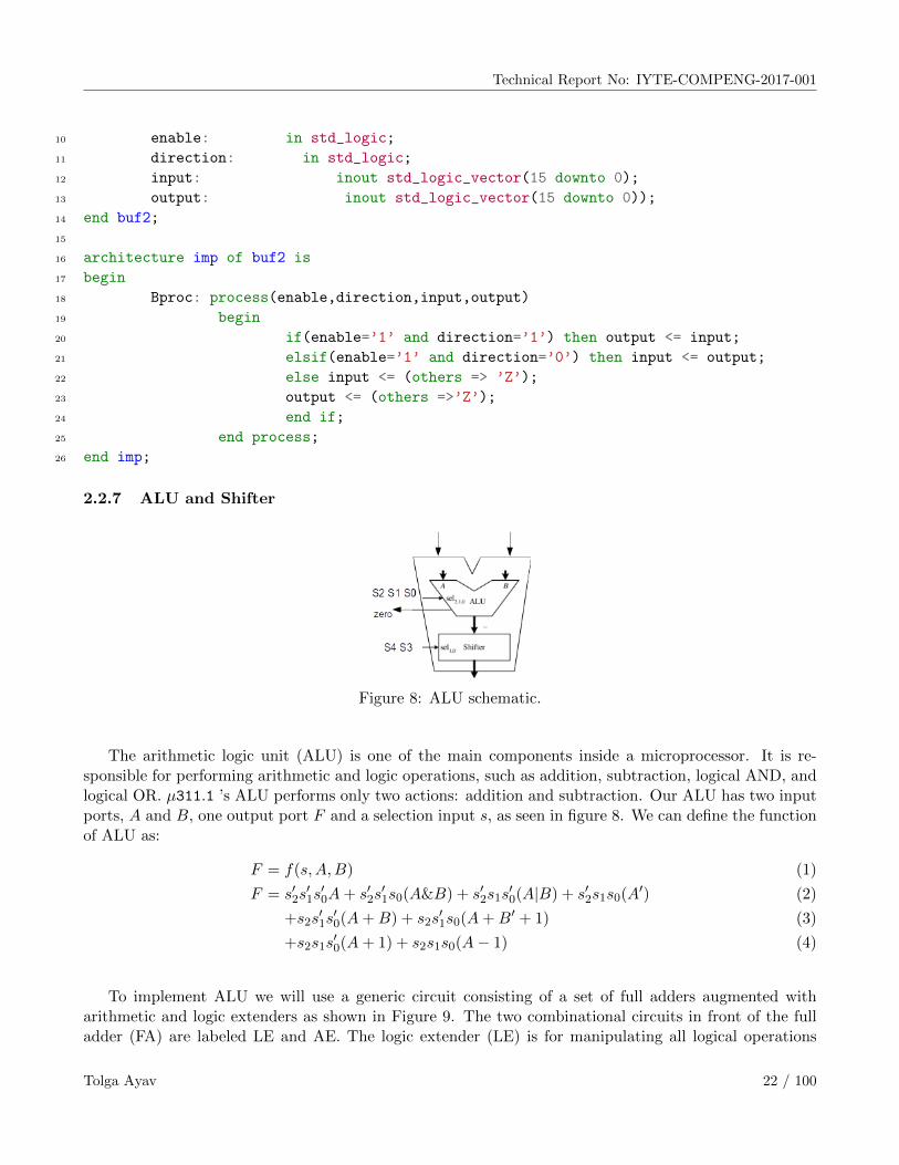
2.2.7 ALU and Shifter
Figure 8: ALU schematic.
The arithmetic logic unit (ALU) is one of the main components inside a microprocessor. It is re-sponsible for performing arithmetic and logic operations, such as addition, subtraction, logical AND, andlogical OR. µ311.1 ’s ALU performs only two actions: addition and subtraction. Our ALU has two inputports, A and B, one output port F and a selection input s, as seen in figure 8. We can define the functionof ALU as:
F = f(s,A,B) (1)
F = s′2s′1s′0A+ s′2s
′1s0(A&B) + s′2s1s
′0(A|B) + s′2s1s0(A′) (2)
+s2s′1s′0(A+B) + s2s
′1s0(A+B′ + 1) (3)
+s2s1s′0(A+ 1) + s2s1s0(A− 1) (4)
To implement ALU we will use a generic circuit consisting of a set of full adders augmented witharithmetic and logic extenders as shown in Figure 9. The two combinational circuits in front of the fulladder (FA) are labeled LE and AE. The logic extender (LE) is for manipulating all logical operations
Tolga Ayav 22 / 100

Technical Report No: IYTE-COMPENG-2017-001
Figure 9: Implementation of ALU (Shown for 8-bits).
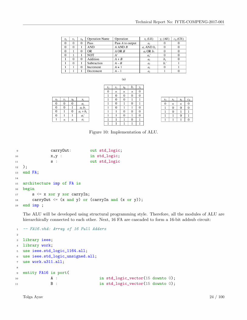
Table 2: ALU operationsNo s2−0 Operation Name Operation xi (LE) yi (AE) c0 (CE)
1 000 Pass Pass A to output ai 0 0
2 001 And A and B ai and bi 0 0
3 010 Or A or B ai or bi 0 0
4 011 Not A′ a′i 0 0
5 100 Addition A+B ai bi 0
6 101 Subtraction A−B ai b′i 1
7 110 Increment A+ 1 ai 0 1
8 111 Decrement A− 1 ai 1 0
whereas the arithmetic extender (AE) is for manipulating all arithmetical operations. The LE performslogical operations on the two primary operands, ai and bi, before passing the result to the first operand,xi, of the FA. On the other hand, the AE only modifies the second operand, bi, and passes it to the secondoperand, yi, of the FA where the actual arithmetical operation is performed. To perform additions andsubtractions, we only need to modify yi (the second operand to the FA) so that all operations can be donewith additions. The combinational circuit labeled CE (for carry extender) is for modifying the primarycarry-in signal, c0, so that arithmetic operations are performed correctly.
Question 4 Design the ALU using common digital design techniques that benefit from truth tables, kar-naugh maps or other simplification methods. The function of ALU is given in table 2.
Below, you can find the necessary VHDL programs to implement the ALU. The first program describesthe full adder circuit:
1 --FA.vhd: Full Adder
2
3 library ieee;
4 use ieee.std_logic_1164.all;
5 use ieee.std_logic_unsigned.all;
6
7 entity FA is port(
8 carryIn: in std_logic;
Tolga Ayav 23 / 100
Technical Report No: IYTE-COMPENG-2017-001
Figure 10: Implementation of ALU.
9 carryOut: out std_logic;
10 x,y : in std_logic;
11 s : out std_logic
12 );
13 end FA;
14
15 architecture imp of FA is
16 begin
17 s <= x xor y xor carryIn;
18 carryOut <= (x and y) or (carryIn and (x or y));
19 end imp ;
The ALU will be developed using structural programming style. Therefore, all the modules of ALU arehierarchically connected to each other. Next, 16 FA are cascaded to form a 16-bit addsub circuit:
1 -- FA16.vhd: Array of 16 Full Adders
2
3 library ieee;
4 library work;
5 use ieee.std_logic_1164.all;
6 use ieee.std_logic_unsigned.all;
7 use work.u311.all;
8
9 entity FA16 is port(
10 A : in std_logic_vector(15 downto 0);
11 B : in std_logic_vector(15 downto 0);
Tolga Ayav 24 / 100

Technical Report No: IYTE-COMPENG-2017-001
12 F : out std_logic_vector(15 downto 0);
13 cIn: in std_logic ;
14 unsigned_overflow: out std_logic;
15 signed_overflow: out std_logic
16 );
17 end FA16;
18
19 architecture imp of FA16 is
20 signal C: std_logic_vector(15 downto 1);
21 begin
22 U0: FA port map(cIn, C(1), A(0), B(0), F(0));
23 U1_14: for I in 1 to 14 generate
24 begin
25 U: FA port map(C(I), C(I+1), A(I), B(I), F(I));
26 end generate U1_14;
27 U15: FA port map(C(15), unsigned_overflow,A(15),B(15),F(15));
28 signed_overflow <= C(15) xor C(14) ;
29 end imp;
The following circuits describe the logical and arithmetical extension parts of the ALU:
1 -- LE.vhd: Logic Extender circuit
2
3 library ieee;
4 use ieee.std_logic_1164.all;
5 use ieee.std_logic_unsigned.all;
6 use ieee.numeric_std.all;
7
8 entity LE is port(
9 S: in std_logic_vector(2 downto 0);
10 a, b: in std_logic;
11 x: out std_logic
12 );
13 end LE;
14
15 architecture imp of LE is
16 begin
17 process(S,a,b)
18 begin
19 case S is
20 when "000" => x <= a;
21 when "001" => x <= a and b;
22 when "010" => x <= a or b;
23 when "011" => x <= not a;
24 when others => x <= a;
25 end case;
26 end process;
Tolga Ayav 25 / 100

Technical Report No: IYTE-COMPENG-2017-001
27 end imp;
1 -- LE16.vhd: Array of 16 LE circuits
2
3 library ieee;
4 library work;
5 use ieee.std_logic_1164.all;
6 use ieee.std_logic_unsigned.all;
7 use ieee.numeric_std.all;
8 use work.u311.LE;
9
10 entity LE16 is port(
11 S: in std_logic_vector(2 downto 0);
12 A, B: in std_logic_vector(15 downto 0);
13 x: out std_logic_vector(15 downto 0)
14 );
15 end LE16;
16
17 architecture imp of LE16 is
18 begin
19 LE16X: for I in 0 to 15 generate
20 LEX: LE port map(S, A(I), B(I), X(I));
21 end generate LE16X;
22 end imp;
1 library ieee;
2 use ieee.std_logic_1164.all;
3 use ieee.std_logic_unsigned.all;
4 use ieee.numeric_std.all;
5
6 entity AE is port(
7 S: in std_logic_vector(2 downto 0);
8 a, b: in std_logic;
9 x: out std_logic
10 );
11 end AE;
12
13
14 architecture imp of AE is
15 begin
16
17 process(S,b)
18 begin
19
20 case S is
21 when "100" => x <= b;
Tolga Ayav 26 / 100

Technical Report No: IYTE-COMPENG-2017-001
22 when "101" => x <= not b;
23 when "110" => x <= ’0’;
24 when "111" => x <= ’1’;
25 when others => x <= ’0’;
26 end case;
27
28 end process;
29
30 end imp;
1 -- AE16.vhd: Array of 16 AE circuits
2
3 library ieee;
4 library work;
5 use ieee.std_logic_1164.all;
6 use ieee.std_logic_unsigned.all;
7 use ieee.numeric_std.all;
8 use work.u311.AE;
9
10 entity AE16 is port(
11 S: in std_logic_vector(2 downto 0);
12 A, B: in std_logic_vector(15 downto 0);
13 Y: out std_logic_vector(15 downto 0)
14 );
15 end AE16;
16
17 architecture imp of AE16 is
18 begin
19 AE16X: for I in 0 to 15 generate
20 AEX: AE port map(S, A(I), B(I), Y(I));
21 end generate AE16X;
22
23 end imp;
The last part of the ALU is the shifter. This allows shifting a given number one bit to the left or right.The shifter is composed of 16 multiplexers:
1 -- shifter.vhd: 16 bit shifter
2
3 library ieee;
4 library work;
5 use ieee.std_logic_1164.all;
6 use ieee.std_logic_unsigned.all;
7 use ieee.numeric_std.all;
8 use work.u311.all;
9
10 entity shifter16 is port(
Tolga Ayav 27 / 100

Technical Report No: IYTE-COMPENG-2017-001
11 S: in std_logic_vector(1 downto 0);
12 A: in std_logic_vector(15 downto 0);
13 Y: out std_logic_vector(15 downto 0);
14 carryOut: out std_logic;
15 zero: out std_logic
16 );
17 end shifter16;
18
19 architecture imp of shifter16 is
20 begin
21 process(S)
22 begin
23 if(S="01") then
24 carryOut <= A(15);
25 elsif(S="10") then
26 carryOut <= A(0);
27 end if;
28 end process;
29
30 U0 : mux port map(S, A(0), ’0’, A(1), A(1), Y(0));
31 U1_14: for I in 1 to 14 generate
32 UX: mux port map(S, A(I), A(I-1), A(I+1), A(I+1), Y(I));
33 end generate U1_14;
34 U15 : mux port map(S, A(15), A(14), ’0’, A(0), Y(15));
35
36 process(A,S)
37 begin
38 if(S="00") then
39 if(A = "0000") then
40 zero <= ’1’;
41 else
42 zero <= ’0’;
43 end if;
44 end if;
45 end process;
46 end imp;
The last step is to bring all these parts together to constitute the ALU as follows:
1 library ieee;
2 use ieee.std_logic_1164.all;
3 use ieee.std_logic_unsigned.all;
4 use ieee.numeric_std.all;
5
6 library work;
7 use work.uP.all;
8
Tolga Ayav 28 / 100

Technical Report No: IYTE-COMPENG-2017-001
9 entity ALU is port(
10 S: in std_logic_vector(4 downto 0);
11 A,B: in std_logic_vector(15 downto 0);
12 F: out std_logic_vector(15 downto 0);
13 unsigned_overflow: out std_logic;
14 signed_overflow: out std_logic;
15 carry: out std_logic);
16 end ALU;
17
18 architecture imp of ALU is
19 signal X,Y,ShiftInput: std_logic_vector(15 downto 0);
20 signal c0: std_logic;
21 begin
22 CarryExtender_ALU: c0 <= (S(0) xor S(1)) and S(2);
23 LogicExtender16_ALU: LE16 port map(S(2 downto 0), A, B, X);
24 ArithmeticExtender16_ALU: AE16 port map(S(2 downto 0), A, B, Y);
25 FA16_ALU: FA16 port map(X, Y, ShiftInput, c0, unsigned_overflow, signed_overflow);
26 Shifter16_ALU: shifter16 port map(S(4 downto 3), ShiftInput, F, carry);
27
28
29 end imp;
Despite its less resource consumption, the structural implementation is really cumbersome. The be-havioural implementation of the ALU, indeed, would be as easy as follows:
1 -- alu2.vhd: Alternative implementation of ALU
2
3 library ieee;
4 library work;
5 use ieee.std_logic_1164.all;
6 use ieee.std_logic_unsigned.all;
7 use ieee.numeric_std.all;
8 use work.u311.all;
9
10 entity ALU_Behavioral is port (
11 S: in std_logic_vector(4 downto 0);
12 A, B: in std_logic_vector(15 downto 0);
13 F: out std_logic_vector(15 downto 0);
14 zero: out std_logic
15 );
16 end ALU_Behavioral;
17
18 architecture imp of ALU_Behavioral is
19 signal X, Y, ShiftInput: std_logic_vector(15 downto 0);
20 signal c0: std_logic;
21 begin
22 ALU: process(S,A,B)
Tolga Ayav 29 / 100
Technical Report No: IYTE-COMPENG-2017-001
23 begin
24 case S is
25 when "00000" => F <= A;
26 when "00100" => F <= A and B;
27 when "01000" => F <= A or B;
28 when "01100" => F <= not A;
29 when "10000" => F <= A + B;
30 when "10100" => F <= A - B;
31 when "11000" => F <= A + 1;
32 when "11100" => F <= A - 1;
33 when "00001" => F <= to_stdlogicvector(to_bitvector(A) sll 1);
34 when "00010" => F <= to_stdlogicvector(to_bitvector(A) srl 1);
35 when "00011" => F(15) <= A(0);
36 F <= to_stdlogicvector(to_bitvector(A) srl 1);
37 when others => F <= "ZZZZZZZZZZZZZZZZ";
38 end case;
39 end process;
40 end imp;
The entire datapath can then be constructed as follows:
1 -- datapath.vhd: Datapath of u311
2
3 library ieee;
4 library work;
5 use ieee.std_logic_1164.all;
6 use ieee.std_logic_unsigned.all;
7 use work.uP.all;
8
9 entity datapath is port(
10 clk: in std_logic;
11 reset : in std_logic;
12 pcen, den, dir, aen: in std_logic;
13 SPload, PCload, IRload: in std_logic;
14 Psel, Ssel, Rsel, Osel : in std_logic_vector(1 downto 0);
15 sub2: in std_logic;
16 jmpMux : in std_logic;
17 IR : out std_logic_vector (4 downto 0);
18 zero: out std_logic;
19 ALUsel : in std_logic_vector (4 downto 0);
20 we, rae, rbe : in std_logic;
21 Buf2_out: out std_logic_vector(15 downto 0);
22 Buf3_out: inout std_logic_vector(15 downto 0)
23 );
24 end dataPath;
25
26 architecture imp of datapath is
Tolga Ayav 30 / 100
Technical Report No: IYTE-COMPENG-2017-001
27 -----------------SIGNALS-------------------
28 signal ALU_out, PC_out, IR_out, SP_out, Pm_out: std_logic_vector(15 downto 0);
29 signal P_out, Add1_out, Add2_out, O_out, S_out, R_out: std_logic_vector(15 downto 0);
30 signal RA, RB: std_logic_vector(15 downto 0);
31 signal int_in, pc_in: std_logic_vector(15 downto 0);
32 signal sub1: std_logic;
33 signal Pm_in: std_logic_vector(15 downto 0);
34 ---------------------------------------------------
35 begin
36
37 int_in <= "000000000" & IR_out(2 downto 0) & "1111";
38 pc_in <= X"00" & IR_out(7 downto 0);
39 IR <= IR_out(15 downto 11);
40 -- Special registers ------------------------------------------
41
42 PCx: reg16 port map(P_out,PCload,reset,clk,PC_out);
43 IRx: reg16 port map(RB,IRload,reset,clk,IR_out);
44 SPx: reg16f port map(S_out,SPload,reset,clk,SP_out);
45
46 --- Multiplexers ----------------------------------------------
47
48 Pmux4: mux4 port map(Psel,int_in,int_in,RB,Add1_out,P_out);
49
50 Rmux4: mux4 port map(Rsel,RA,SP_out,RB,pc_in,R_out);
51
52 Smux4: mux4 port map(Ssel,X"0000",X"0000",RA,Add2_out,S_out);
53 Omux4: mux4 port map(Osel,PC_out,SP_out,X"0000",RA,O_out);
54 Pm_in <= "000000" & IR_out(9 downto 0);
55 Pmux2: mux2 port map(jmpMux,X"0001",Pm_in,Pm_out);
56
57 ---- ALU and Regfile------------------------------------------------
58 Regf: regfile port map(clk,reset,we,IR_out(10 downto 8),ALU_out,rbe,rae,IR_out(7 downto 5),IR_out(4 downto 2),RA,RB);
59 ALUx: alu port map(ALUsel,R_out,RB,ALU_out,open,open,open);
60 --------------------------------------------------------------------
61 -- zero flag !!
62 process(ALU_out)
63 begin
64 if(IR_out(15 downto 11) ="00001" or IR_out(15 downto 11) = "00111" or IR_out(15 downto 11) = "00010" or IR_out(15 downto 11) = "00110") then
65 if (ALU_out = "0000") then
66 zero <=’1’;
67 else
68 zero <=’0’;
69 end if;
70 end if;
71 end process;
72 ---- Buffers -------------------------------------------------------
Tolga Ayav 31 / 100

Technical Report No: IYTE-COMPENG-2017-001
73 Buf1x: buf port map(pcen,PC_out,Buf3_out);
74 Buf2x: buf port map(aen,O_out,Buf2_out);
75 Buf3x: buf2 port map(den,dir,RB,Buf3_out);
76 ---- Addsub circuits -----------------------------------------------
77 sub1 <= IR_out(10) and jmpMux;
78 Addsub1: addsub16 port map(sub1,PC_out,Pm_out,Add1_out);
79 Addsub2: addsub16 port map(sub2,SP_out,X"0001",Add2_out);
80 --------------------------------------------------------------------
81 end imp;
2.2.8 The processor
1 -- u311_1.vhd: Microprocessor
2
3 library ieee;
4 library work;
5 use ieee.std_logic_1164.all;
6 use ieee.std_logic_unsigned.all;
7 use ieee.numeric_std.all;
8 use work.uP.all;
9
10 entity u311_1 is port(
11 clk: in std_logic;
12 reset: in std_logic;
13
14 opfetch: out std_logic;
15 INT: in std_logic;
16 INTA: out std_logic;
17 WR: out std_logic;
18 RD: out std_logic;
19 A: out std_logic_vector(15 downto 0);
20 D: inout std_logic_vector(15 downto 0));
21
22 end u311_1;
23
24 architecture imp of u311_1 is
25
26 signal pcen,aen,den,dir: std_logic;
27 signal SPload,IRload,PCload: std_logic;
28 signal Psel,Ssel,Rsel,Osel : std_logic_vector(1 downto 0);
29 signal IR: std_logic_vector(4 downto 0);
30 signal we,rae,rbe: std_logic;
31 signal ALUsel: std_logic_vector(4 downto 0);
32 signal zero: std_logic;
33 signal sub2: std_logic;
34 signal jmpMux: std_logic;
Tolga Ayav 32 / 100

Technical Report No: IYTE-COMPENG-2017-001
35
36 begin
37 CU: controller port map(clk,reset,pcen,den,dir,aen,SPload,PCload,IRload,Psel,Ssel,Rsel,Osel,sub2,jmpMux,opfetch,IR,zero,ALUsel,we,rae,rbe,int,inta,wr,rd);
38 DP: datapath port map(clk,reset,pcen,den,dir,aen,SPload,PCload,IRload,Psel,Ssel,Rsel,Osel,sub2,jmpMux,IR,zero,ALUsel,we,rae,rbe,A,D);
39 end imp;
2.3 Stack
Stack region can be defined in the external memory. Stack pointer register SP must be initialized for this.Recall that SP holds 0x0000 after a reset. An appropriate value could be for example 0x00FF . Thisinitialization can be done with the following code:
1 mov a, ffh
2 mov c, 08h
3 L: sl a
4 dec c
5 jnz L
6 mob b, ffh
7 add a,a,b
8 mov sp, a
Question 5 Assume that the first instruction of the program is “pop a”. In this case, what would registerA holds after this command?
2.4 Control Unit
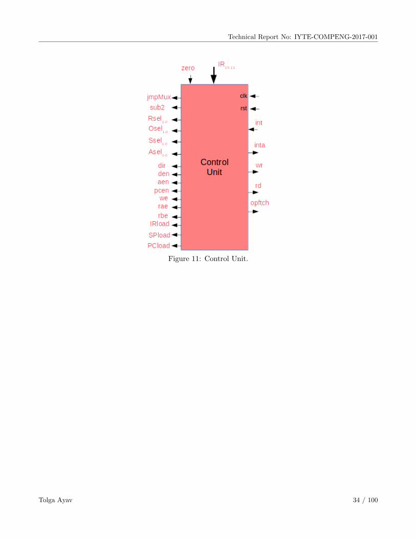
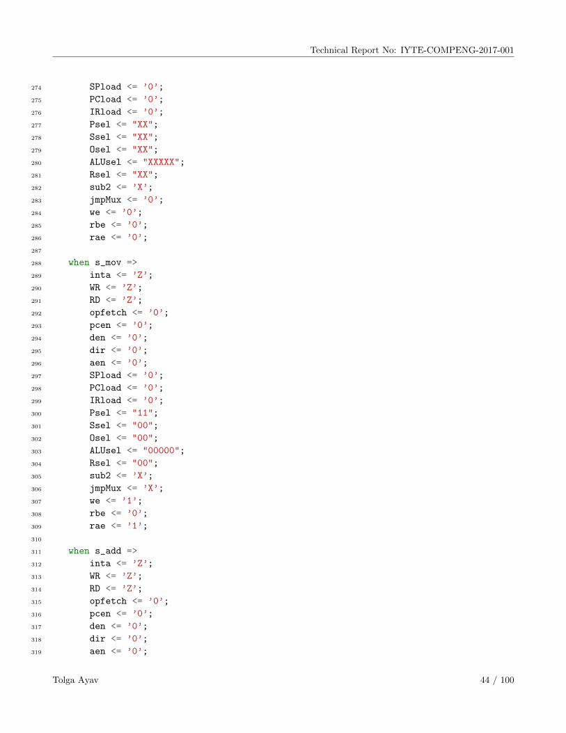
The control unit inside the microprocessor is a finite state machine. By stepping through a sequence ofstates, the control unit controls the operations of the datapath. For each state that the control unit isin, the output logic that is inside the control unit will generate all of the appropriate control signals forthe datapath to perform one data operation. These data operations are referred to as register-transferoperations. Each register-transfer operation consists of reading a value from a register, modifying thevalue by one or more functional units, and finally, writing the modified value back into the same or adifferent register.
The block diagram of our control unit is given in figure 11. Figure 12 shows the FSM of µ311.1 .
Tolga Ayav 33 / 100
Technical Report No: IYTE-COMPENG-2017-001
Figure 11: Control Unit.
Tolga Ayav 34 / 100

Technical Report No: IYTE-COMPENG-2017-001
Figure 12: FSM diagram for the control unit.
2.4.1 Bus Cycles
µ311.1 has 4 cycles: opcode fetch, read, write and interrupt. The timing diagram for each cycle is givenbelow.
Tolga Ayav 35 / 100

Technical Report No: IYTE-COMPENG-2017-001
1. Opcode Fetch Cycle
Figure 13: Opcode fetch cycle
2. Memory/IO Read Cycle
Figure 14: Memory - I/O read cycle
Tolga Ayav 36 / 100

Technical Report No: IYTE-COMPENG-2017-001
3. Memory/IO Write Cycle
Figure 15: Memory - I/O write cycle
4. Interrupt Cycle
Figure 16: Interrupt cycle
Tolga Ayav 37 / 100

Technical Report No: IYTE-COMPENG-2017-001
Question 6 Complete the next-state diagram of the control unit given in the table 3 and design the controlunit using J-K flip-flops.
1 -- controller.vhd: control unit
2 library ieee;
3 library work;
4 use IEEE.std_logic_1164.all;
5 use IEEE.std_logic_textio.all;
6 use IEEE.std_logic_arith.all;
7 use IEEE.numeric_bit.all;
8 use IEEE.numeric_std.all;
9 use IEEE.std_logic_signed.all;
10 use IEEE.std_logic_unsigned.all;
11 use IEEE.math_real.all;
12 use IEEE.math_complex.all;
13 use work.uP.all;
14
15 entity controller is port(
16 clk: in std_logic;
17 reset : in std_logic;
18 pcen, den, dir, aen: out std_logic;
19 SPload, PCload, IRload: out std_logic;
20 Psel, Ssel, Rsel, Osel : out std_logic_vector(1 downto 0);
21 sub2: out std_logic;
22 jmpMux : out std_logic;
23 opfetch : out std_logic;
24 IR : in std_logic_vector (4 downto 0);
25 zero: in std_logic;
26 ALUsel : out std_logic_vector (4 downto 0);
27 we, rae, rbe : out std_logic;
28 int: in std_logic;
29 inta, wr, rd: out std_logic);
30 end controller;
31
32 architecture imp of controller is
33 type state_type is (
34 s_strt,
35 s_ftch,
36 s_dcd,
37 s_dcd2,
38 s_mov,
39 s_add,
40 s_sub,
41 s_and,
42 s_or,
43 s_not,
Tolga Ayav 38 / 100
Technical Report No: IYTE-COMPENG-2017-001
44 s_inc,
45 s_dec,
46 s_sr,
47 s_sl,
48 s_rr,
49 s_clr,
50 s_jmp,
51 s_call,
52 s_ret,
53 s_nop,
54 s_halt,
55 s_psh,
56 s_psh2,
57 s_pop,
58 s_pop2,
59 s_wrt,
60 s_read,
61 s_movi,
62 s_mvspr,
63 s_mvrsp,
64 s_r_c1,
65 s_r_c2,
66 s_r_c3,
67 s_w_c1,
68 s_w_c2,
69 s_w_c3,
70 s_int_c1,
71 s_int_c2,
72 s_int_c3);
73
74 signal state: state_type :=s_strt;
75 signal zero_flag: std_logic;
76
77 begin
78
79 NEXT_STATE_LOGIC: process(clk, reset)
80 variable int_occr : boolean := false;
81 begin
82
83 if(reset =’1’) then
84 state <= s_strt;
85 elsif (int =’1’) then
86 int_occr := true;
87 elsif(clk’event and clk=’1’) then
88
89 case state is
Tolga Ayav 39 / 100

Technical Report No: IYTE-COMPENG-2017-001
90 when s_strt => state <= s_ftch after 1ns;
91 when s_ftch => state <= s_dcd after 1ns;
92 when s_dcd2 =>
93
94 case IR is
95 when "00000" => state <= s_mov after 1ns;
96 when "00001" => state <= s_add after 1ns;
97 when "00010" => state <= s_sub after 1ns;
98 when "00011" => state <= s_and after 1ns;
99 when "00100" => state <= s_or after 1ns;
100 when "00101" => state <= s_not after 1ns;
101 when "00110" => state <= s_inc after 1ns;
102 when "00111" => state <= s_dec after 1ns;
103 when "01000" => state <= s_sr after 1ns;
104 when "01001" => state <= s_sl after 1ns;
105 when "01010" => state <= s_rr after 1ns;
106 when "01011" => state <= s_jmp after 1ns;
107 when "01100" => if(zero_flag = ’1’) then state <= s_jmp after 1ns;
108 elsif(zero_flag = ’0’) then state <= s_nop after 1ns;
109 end if;
110 when "01101" => if(zero_flag = ’0’) then state <= s_jmp after 1ns;
111 elsif(zero_flag = ’1’) then state <= s_nop after 1ns;
112 end if;
113 when "01110" => state <= s_call after 1ns;
114 when "01111" => state <= s_ret after 1ns;
115 when "10000" => state <= s_nop after 1ns;
116 when "10001" => state <= s_halt after 1ns;
117 when "10010" => state <= s_psh after 1ns;
118 when "10011" => state <= s_pop after 1ns;
119 when "10100" => state <= s_wrt after 1ns;
120 when "10101" => state <= s_read after 1ns;
121 when "10110" => state <= s_movi after 1ns;
122 when "10111" => state <= s_mvspr after 1ns;
123 when "11000" => state <= s_mvrsp after 1ns;
124 when others =>
125
126 state <= s_strt after 1us;
127 end case;
128
129 when s_halt => state <= s_halt after 1ns;
130 when s_wrt => state <= s_w_c1 after 1ns;
131 when s_read => state <= s_r_c1 after 1ns;
132 when s_w_c1 => state <= s_w_c2 after 1ns;
133 when s_r_c1 => state <= s_r_c2 after 1ns;
134 when s_w_c2 => state <= s_w_c3 after 1ns;
135 when s_r_c2 => state <= s_r_c3 after 1ns;
Tolga Ayav 40 / 100

Technical Report No: IYTE-COMPENG-2017-001
136 when s_int_c1 => state <= s_int_c2 after 1ns;
137 when s_int_c2 => state <= s_int_c3 after 1ns;
138
139 when others =>
140 if(int_occr = true) then
141 state <= s_int_c1 after 1ns;
142 inta <= ’1’ after 1ns;
143 int_occr := false;
144
145 elsif(int_occr = false) then
146 state <= s_ftch after 1ns;
147 end if;
148
149 end case;
150
151 elsif(clk’event and clk=’0’) then
152 case state is
153 when s_psh => state <= s_psh2 after 1ns;
154 when s_pop => state <= s_pop2 after 1ns;
155 when s_dcd => state <= s_dcd2 after 1ns;
156 when others =>
157 end case;
158 end if;
159 end process;
160
161 OUTPUT_LOGIC: process(state)
162 begin
163
164 case state is
165
166 when s_strt =>
167 inta <= ’Z’;
168 WR <= ’Z’;
169 RD <= ’Z’;
170 opfetch <= ’Z’;
171 pcen <= ’0’;
172 den <= ’0’;
173 dir <= ’0’;
174 aen <= ’0’;
175 SPload <= ’0’;
176 PCload <= ’0’;
177 IRload <= ’0’;
178 Psel <= "XX";
179 Ssel <= "XX";
180 Osel <= "XX";
181 ALUsel <= "XXXXX";
Tolga Ayav 41 / 100

Technical Report No: IYTE-COMPENG-2017-001
182 Rsel <= "XX";
183 sub2 <= ’X’;
184 jmpMux <= ’X’;
185 we <= ’0’;
186 rbe <= ’0’;
187 rae <= ’0’;
188
189 when s_ftch =>
190 case IR is
191 when "00001" =>
192 if(zero=’1’) then zero_flag <= ’1’;
193 else zero_flag <= ’0’;
194 end if;
195
196 when "00111" =>
197 if(zero=’1’) then zero_flag <= ’1’;
198 else zero_flag <= ’0’;
199 end if;
200
201 when "00010" =>
202 if(zero=’1’) then zero_flag <= ’1’;
203 else zero_flag <= ’0’;
204 end if;
205
206 when "00110" =>
207 if(zero=’1’) then zero_flag <= ’1’;
208 else zero_flag <= ’0’;
209 end if;
210 when others =>
211 end case;
212 inta <= ’Z’;
213 WR <= ’Z’;
214 RD <= ’Z’;
215 opfetch <= ’1’ after 2ns;
216 pcen <= ’0’;
217 den <= ’1’;
218 dir <= ’0’;
219 aen <= ’1’;
220 SPload <= ’0’;
221 PCload <= ’1’;
222 IRload <= ’1’;
223 Psel <= "11";
224 Ssel <= "00";
225 Osel <= "00";
226 ALUsel <= "XXXXX";
227 Rsel <= "XX";
Tolga Ayav 42 / 100

Technical Report No: IYTE-COMPENG-2017-001
228 sub2 <= ’X’;
229 jmpMux <= ’0’;
230 we <= ’0’;
231 rbe <= ’0’;
232 rae <= ’0’;
233
234 when s_dcd =>
235 inta <= ’Z’;
236 WR <= ’Z’;
237 RD <= ’Z’;
238 opfetch <= ’0’;
239 pcen <= ’0’;
240 den <= ’0’;
241 dir <= ’0’;
242 aen <= ’0’;
243
244 case IR is
245 when "10011" => SPload <=’1’; -- for pop inst.
246 sub2 <= ’0’;
247 when "01111" => SPload <= ’1’;-- for ret inst.
248 sub2 <= ’0’;
249 when others => SPload <=’0’;
250 sub2 <= ’X’;
251 end case;
252 PCload <= ’0’;
253 IRload <= ’0’;
254 Psel <= "XX";
255 Ssel <= "11";
256 Osel <= "XX";
257 ALUsel <= "XXXXX";
258 Rsel <= "XX";
259 sub2 <= ’0’;
260 jmpMux <= ’0’;
261 we <= ’0’;
262 rbe <= ’0’;
263 rae <= ’0’;
264
265 when s_dcd2 =>
266 inta <= ’Z’;
267 WR <= ’Z’;
268 RD <= ’Z’;
269 opfetch <= ’0’;
270 pcen <= ’0’;
271 den <= ’0’;
272 dir <= ’0’;
273 aen <= ’0’;
Tolga Ayav 43 / 100
Technical Report No: IYTE-COMPENG-2017-001
274 SPload <= ’0’;
275 PCload <= ’0’;
276 IRload <= ’0’;
277 Psel <= "XX";
278 Ssel <= "XX";
279 Osel <= "XX";
280 ALUsel <= "XXXXX";
281 Rsel <= "XX";
282 sub2 <= ’X’;
283 jmpMux <= ’0’;
284 we <= ’0’;
285 rbe <= ’0’;
286 rae <= ’0’;
287
288 when s_mov =>
289 inta <= ’Z’;
290 WR <= ’Z’;
291 RD <= ’Z’;
292 opfetch <= ’0’;
293 pcen <= ’0’;
294 den <= ’0’;
295 dir <= ’0’;
296 aen <= ’0’;
297 SPload <= ’0’;
298 PCload <= ’0’;
299 IRload <= ’0’;
300 Psel <= "11";
301 Ssel <= "00";
302 Osel <= "00";
303 ALUsel <= "00000";
304 Rsel <= "00";
305 sub2 <= ’X’;
306 jmpMux <= ’X’;
307 we <= ’1’;
308 rbe <= ’0’;
309 rae <= ’1’;
310
311 when s_add =>
312 inta <= ’Z’;
313 WR <= ’Z’;
314 RD <= ’Z’;
315 opfetch <= ’0’;
316 pcen <= ’0’;
317 den <= ’0’;
318 dir <= ’0’;
319 aen <= ’0’;
Tolga Ayav 44 / 100

Technical Report No: IYTE-COMPENG-2017-001
320 SPload <= ’0’;
321 PCload <= ’0’;
322 IRload <= ’0’;
323 Psel <= "11";
324 Ssel <= "00";
325 Osel <= "00";
326 ALUsel <= "00100";
327 Rsel <= "00";
328 sub2 <= ’X’;
329 jmpMux <= ’0’;
330 we <= ’1’;
331 rbe <= ’1’;
332 rae <= ’1’;
333
334 when s_sub =>
335 inta <= ’Z’;
336 WR <= ’Z’;
337 RD <= ’Z’;
338 opfetch <= ’0’;
339 pcen <= ’0’;
340 den <= ’0’;
341 dir <= ’0’;
342 aen <= ’0’;
343 SPload <= ’0’;
344 PCload <= ’0’;
345 IRload <= ’0’;
346 Psel <= "11";
347 Ssel <= "00";
348 Osel <= "00";
349 ALUsel <= "00101";
350 Rsel <= "00";
351 sub2 <= ’X’;
352 jmpMux <= ’0’;
353 we <= ’1’;
354 rbe <= ’1’;
355 rae <= ’1’;
356
357 when s_and =>
358 inta <= ’Z’;
359 WR <= ’Z’;
360 RD <= ’Z’;
361 opfetch <= ’0’;
362 pcen <= ’0’;
363 den <= ’0’;
364 dir <= ’0’;
365 aen <= ’0’;
Tolga Ayav 45 / 100

Technical Report No: IYTE-COMPENG-2017-001
366 SPload <= ’0’;
367 PCload <= ’0’;
368 IRload <= ’0’;
369 Psel <= "11";
370 Ssel <= "00";
371 Osel <= "00";
372 ALUsel <= "00001";
373 Rsel <= "00";
374 sub2 <= ’X’;
375 jmpMux <= ’0’;
376 we <= ’1’;
377 rbe <= ’1’;
378 rae <= ’1’;
379
380 when s_or =>
381 inta <= ’Z’;
382 WR <= ’Z’;
383 RD <= ’Z’;
384 opfetch <= ’0’;
385 pcen <= ’0’;
386 den <= ’0’;
387 dir <= ’0’;
388 aen <= ’0’;
389 SPload <= ’0’;
390 PCload <= ’0’;
391 IRload <= ’0’;
392 Psel <= "11";
393 Ssel <= "00";
394 Osel <= "00";
395 ALUsel <= "00010";
396 Rsel <= "00";
397 sub2 <= ’X’;
398 jmpMux <= ’0’;
399 we <= ’1’;
400 rbe <= ’1’;
401 rae <= ’1’;
402
403 when s_not =>
404 inta <= ’Z’;
405 WR <= ’Z’;
406 RD <= ’Z’;
407 opfetch <= ’0’;
408 pcen <= ’0’;
409 den <= ’1’;
410 dir <= ’1’;
411 aen <= ’0’;
Tolga Ayav 46 / 100
Technical Report No: IYTE-COMPENG-2017-001
412 SPload <= ’0’;
413 PCload <= ’0’;
414 IRload <= ’0’;
415 Psel <= "11";
416 Ssel <= "00";
417 Osel <= "00";
418 ALUsel <= "00011";
419 Rsel <= "00";
420 sub2 <= ’X’;
421 jmpMux <= ’0’;
422 we <= ’1’;
423 rbe <= ’0’;
424 rae <= ’1’;
425
426 when s_inc =>
427 inta <= ’Z’;
428 WR <= ’Z’;
429 RD <= ’Z’;
430 opfetch <= ’0’;
431 pcen <= ’0’;
432 den <= ’1’;
433 dir <= ’1’;
434 aen <= ’0’;
435 SPload <= ’0’;
436 PCload <= ’0’;
437 IRload <= ’0’;
438 Psel <= "11";
439 Ssel <= "00";
440 Osel <= "00";
441 ALUsel <= "00110";
442 Rsel <= "00";
443 sub2 <= ’X’;
444 jmpMux <= ’0’;
445 we <= ’1’;
446 rbe <= ’0’;
447 rae <= ’1’;
448
449 when s_dec =>
450 inta <= ’Z’;
451 WR <= ’Z’;
452 RD <= ’Z’;
453 opfetch <= ’0’;
454 pcen <= ’0’;
455 den <= ’1’;
456 dir <= ’1’;
457 aen <= ’0’;
Tolga Ayav 47 / 100

Technical Report No: IYTE-COMPENG-2017-001
458 SPload <= ’0’;
459 PCload <= ’0’;
460 IRload <= ’0’;
461 Psel <= "11";
462 Ssel <= "00";
463 Osel <= "00";
464 ALUsel <= "00111";
465 Rsel <= "00";
466 sub2 <= ’X’;
467 jmpMux <= ’0’;
468 we <= ’1’;
469 rbe <= ’0’;
470 rae <= ’1’;
471
472 when s_sr =>
473 inta <= ’Z’;
474 WR <= ’Z’;
475 RD <= ’Z’;
476 opfetch <= ’0’;
477 pcen <= ’0’;
478 den <= ’1’;
479 dir <= ’1’;
480 aen <= ’0’;
481 SPload <= ’0’;
482 PCload <= ’0’;
483 IRload <= ’0’;
484 Psel <= "11";
485 Ssel <= "00";
486 Osel <= "00";
487 ALUsel <= "10000";
488 Rsel <= "00";
489 sub2 <= ’X’;
490 jmpMux <= ’0’;
491 we <= ’1’;
492 rbe <= ’0’;
493 rae <= ’1’;
494
495 when s_sl =>
496 inta <= ’Z’;
497 WR <= ’Z’;
498 RD <= ’Z’;
499 opfetch <= ’0’;
500 pcen <= ’0’;
501 den <= ’1’;
502 dir <= ’1’;
503 aen <= ’0’;
Tolga Ayav 48 / 100

Technical Report No: IYTE-COMPENG-2017-001
504 SPload <= ’0’;
505 PCload <= ’0’;
506 IRload <= ’0’;
507 Psel <= "11";
508 Ssel <= "00";
509 Osel <= "00";
510 ALUsel <= "01000";
511 Rsel <= "00";
512 sub2 <= ’X’;
513 jmpMux <= ’0’;
514 we <= ’1’;
515 rbe <= ’0’;
516 rae <= ’1’;
517
518 when s_rr =>
519 inta <= ’Z’;
520 WR <= ’Z’;
521 RD <= ’Z’;
522 opfetch <= ’0’;
523 pcen <= ’0’;
524 den <= ’1’;
525 dir <= ’1’;
526 aen <= ’0’;
527 SPload <= ’0’;
528 PCload <= ’0’;
529 IRload <= ’0’;
530 Psel <= "11";
531 Ssel <= "00";
532 Osel <= "00";
533 ALUsel <= "11000";
534 Rsel <= "00";
535 sub2 <= ’X’;
536 jmpMux <= ’0’;
537 we <= ’1’;
538 rbe <= ’0’;
539 rae <= ’1’;
540
541 when s_jmp =>
542 inta <= ’Z’;
543 WR <= ’Z’;
544 RD <= ’Z’;
545 opfetch <= ’0’;
546 pcen <= ’0’;
547 den <= ’0’;
548 dir <= ’0’;
549 aen <= ’0’;
Tolga Ayav 49 / 100
Technical Report No: IYTE-COMPENG-2017-001
550 SPload <= ’0’;
551 PCload <= ’1’;
552 IRload <= ’0’;
553 Psel <= "11";
554 Ssel <= "XX";
555 Osel <= "XX";
556 ALUsel <= "00000";
557 Rsel <= "XX";
558 sub2 <= ’X’;
559 jmpMux <= ’1’;
560 we <= ’0’;
561 rbe <= ’0’;
562 rae <= ’0’;
563
564 when s_call =>
565 inta <= ’Z’;
566 WR <= ’1’;
567 RD <= ’0’;
568 opfetch <= ’0’;
569 pcen <= ’1’;
570 den <= ’1’;
571 dir <= ’1’;
572 aen <= ’1’;
573 SPload <= ’1’;
574 PCload <= ’1’;
575 IRload <= ’0’;
576 Psel <= "11";
577 Ssel <= "11";
578 Osel <= "01";
579 ALUsel <= "00000";
580 Rsel <= "XX";
581 sub2 <= ’1’;
582 jmpMux <= ’1’;
583 we <= ’0’;
584 rbe <= ’0’;
585 rae <= ’0’;
586
587 when s_ret =>
588 inta <= ’Z’;
589 WR <= ’0’;
590 RD <= ’1’;
591 opfetch <= ’0’;
592 pcen <= ’0’;
593 den <= ’1’;
594 dir <= ’0’;
595 aen <= ’1’;
Tolga Ayav 50 / 100

Technical Report No: IYTE-COMPENG-2017-001
596 SPload <= ’0’;
597 PCload <= ’1’;
598 IRload <= ’0’;
599 Psel <= "10";
600 Ssel <= "11";
601 Osel <= "01";
602 ALUsel <= "XXXXX";
603 Rsel <= "XX";
604 sub2 <= ’0’;
605 jmpMux <= ’0’;
606 we <= ’0’;
607 rbe <= ’0’;
608 rae <= ’0’;
609
610 when s_nop =>
611 inta <= ’Z’;
612 WR <= ’Z’;
613 RD <= ’Z’;
614 opfetch <= ’0’;
615 pcen <= ’0’;
616 den <= ’0’;
617 dir <= ’0’;
618 aen <= ’0’;
619 SPload <= ’0’;
620 PCload <= ’0’;
621 IRload <= ’0’;
622 Psel <= "11";
623 Ssel <= "00";
624 Osel <= "00";
625 ALUsel <= "00000";
626 Rsel <= "XX";
627 sub2 <= ’X’;
628 jmpMux <= ’0’;
629 we <= ’0’;
630 rbe <= ’0’;
631 rae <= ’0’;
632
633 when s_halt =>
634 inta <= ’X’;
635 WR <= ’X’;
636 RD <= ’X’;
637 opfetch <= ’X’;
638 pcen <= ’X’;
639 den <= ’X’;
640 dir <= ’X’;
641 aen <= ’X’;
Tolga Ayav 51 / 100

Technical Report No: IYTE-COMPENG-2017-001
642 SPload <= ’X’;
643 PCload <= ’X’;
644 IRload <= ’X’;
645 Psel <= "XX";
646 Ssel <= "XX";
647 Osel <= "XX";
648 ALUsel <= "XXXXX";
649 Rsel <= "XX";
650 sub2 <= ’X’;
651 jmpMux <= ’X’;
652 we <= ’X’;
653 rbe <= ’X’;
654 rae <= ’X’;
655
656 when s_psh =>
657 inta <= ’Z’;
658 WR <= ’1’;
659 RD <= ’0’;
660 opfetch <= ’0’;
661 pcen <= ’0’;
662 den <= ’1’;
663 dir <= ’1’;
664 aen <= ’1’;
665 SPload <= ’1’;
666 PCload <= ’0’;
667 IRload <= ’0’;
668 Psel <= "11";
669 Ssel <= "11";
670 Osel <= "01";
671 ALUsel <= "00000";
672 Rsel <= "00"; -- IR
673 sub2 <= ’1’;
674 jmpMux <= ’0’;
675 we <= ’0’;
676 rbe <= ’1’;
677 rae <= ’0’;
678 when s_psh2 =>
679 inta <= ’Z’;
680 WR <= ’0’;
681 RD <= ’0’;
682 opfetch <= ’0’;
683 pcen <= ’0’;
684 den <= ’0’;
685 dir <= ’0’;
686 aen <= ’0’;
687 SPload <= ’0’;
Tolga Ayav 52 / 100
Technical Report No: IYTE-COMPENG-2017-001
688 PCload <= ’0’;
689 IRload <= ’0’;
690 Psel <= "11";
691 Ssel <= "11";
692 Osel <= "00";
693 ALUsel <= "00000";
694 Rsel <= "00"; -- IR
695 sub2 <= ’1’;
696 jmpMux <= ’0’;
697 we <= ’0’;
698 rbe <= ’0’;
699 rae <= ’0’;
700
701 when s_pop =>
702 inta <= ’Z’;
703 WR <= ’0’;
704 RD <= ’1’;
705 opfetch <= ’0’;
706 pcen <= ’0’;
707 den <= ’1’;
708 dir <= ’0’;
709 aen <= ’1’;
710 SPload <= ’0’;
711 PCload <= ’0’;
712 IRload <= ’0’;
713 Psel <= "10";
714 Ssel <= "11";
715 Osel <= "01";
716 ALUsel <= "00000";
717 Rsel <= "11";
718 sub2 <= ’0’;
719 jmpMux <= ’0’;
720 we <= ’1’;
721 rbe <= ’0’;
722 rae <= ’0’;
723
724 when s_pop2 =>
725 inta <= ’Z’;
726 WR <= ’0’;
727 RD <= ’1’;
728 opfetch <= ’0’;
729 pcen <= ’0’;
730 den <= ’1’;
731 dir <= ’0’;
732 aen <= ’1’;
733 SPload <= ’0’;
Tolga Ayav 53 / 100

Technical Report No: IYTE-COMPENG-2017-001
734 PCload <= ’0’;
735 IRload <= ’0’;
736 Psel <= "11";
737 Ssel <= "11";
738 Osel <= "01";
739 ALUsel <= "00000";
740 Rsel <= "10";
741 sub2 <= ’0’;
742 jmpMux <= ’0’;
743 we <= ’1’;
744 rbe <= ’0’;
745 rae <= ’0’;
746
747
748 when s_wrt =>
749 inta <= ’Z’;
750 WR <= ’1’;
751 RD <= ’0’;
752 opfetch <= ’0’;
753 pcen <= ’0’;
754 den <= ’1’;
755 dir <= ’1’;
756 aen <= ’1’;
757 SPload <= ’0’;
758 PCload <= ’0’;
759 IRload <= ’0’;
760 Psel <= "11";
761 Ssel <= "00";
762 Osel <= "11";
763 ALUsel <= "ZZZZZ";
764 Rsel <= "ZZ";
765 sub2 <= ’Z’;
766 jmpMux <= ’Z’;
767 we <= ’0’;
768 rbe <= ’1’;
769 rae <= ’1’;
770
771 when s_read =>
772 inta <= ’Z’;
773 WR <= ’Z’;
774 RD <= ’1’;
775 opfetch <= ’Z’;
776 pcen <= ’0’;
777 den <= ’1’;
778 dir <= ’0’;
779 aen <= ’1’;
Tolga Ayav 54 / 100

Technical Report No: IYTE-COMPENG-2017-001
780 SPload <= ’0’;
781 PCload <= ’0’;
782 IRload <= ’0’;
783 Psel <= "11";
784 Ssel <= "00";
785 Osel <= "11";
786 ALUsel <= "00000";
787 Rsel <= "11";
788 sub2 <= ’X’;
789 jmpMux <= ’X’;
790 we <= ’1’;
791 rbe <= ’0’;
792 rae <= ’1’;
793
794 when s_movi =>
795 inta <= ’Z’;
796 WR <= ’Z’;
797 RD <= ’Z’;
798 opfetch <= ’0’;
799 pcen <= ’0’;
800 den <= ’0’;
801 dir <= ’0’;
802 aen <= ’0’;
803 SPload <= ’0’;
804 PCload <= ’0’;
805 IRload <= ’0’;
806 Psel <= "11";
807 Ssel <= "00";
808 Osel <= "00";
809 ALUsel <= "00000";
810 Rsel <= "11";
811 sub2 <= ’X’;
812 jmpMux <= ’0’;
813 we <= ’1’;
814 rbe <= ’0’;
815 rae <= ’0’;
816
817
818 when s_mvspr =>
819 inta <= ’Z’;
820 WR <= ’Z’;
821 RD <= ’Z’;
822 opfetch <= ’0’;
823 pcen <= ’0’;
824 den <= ’0’;
825 dir <= ’0’;
Tolga Ayav 55 / 100
Technical Report No: IYTE-COMPENG-2017-001
826 aen <= ’0’;
827 SPload <= ’1’;
828 PCload <= ’0’;
829 IRload <= ’0’;
830 Psel <= "11";
831 Ssel <= "10";
832 Osel <= "ZZ";
833 ALUsel <= "ZZZZZ";
834 Rsel <= "ZZ";
835 sub2 <= ’X’;
836 jmpMux <= ’0’;
837 we <= ’0’;
838 rbe <= ’0’;
839 rae <= ’1’;
840 when s_mvrsp =>
841 inta <= ’Z’;
842 WR <= ’Z’;
843 RD <= ’Z’;
844 opfetch <= ’0’;
845 pcen <= ’0’;
846 den <= ’0’;
847 dir <= ’0’;
848 aen <= ’0’;
849 SPload <= ’0’;
850 PCload <= ’0’;
851 IRload <= ’0’;
852 Psel <= "11";
853 Ssel <= "ZZ";
854 Osel <= "ZZ";
855 ALUsel <= "00000";
856 Rsel <= "01";
857 sub2 <= ’X’;
858 jmpMux <= ’0’;
859 we <= ’1’;
860 rbe <= ’0’;
861 rae <= ’0’;
862
863 when s_r_c1 =>
864 inta <= ’Z’;
865 WR <= ’Z’;
866 RD <= ’1’;
867 opfetch <= ’Z’;
868 pcen <= ’0’;
869 den <= ’1’;
870 dir <= ’0’;
871 aen <= ’1’;
Tolga Ayav 56 / 100

Technical Report No: IYTE-COMPENG-2017-001
872 SPload <= ’0’;
873 PCload <= ’0’;
874 IRload <= ’0’;
875 Psel <= "11";
876 Ssel <= "00";
877 Osel <= "11";
878 ALUsel <= "00000";
879 Rsel <= "11";
880 sub2 <= ’X’;
881 jmpMux <= ’X’;
882 we <= ’1’;
883 rbe <= ’0’;
884 rae <= ’1’;
885 when s_r_c2 =>
886 inta <= ’Z’;
887 WR <= ’Z’;
888 RD <= ’1’;
889 opfetch <= ’Z’;
890 pcen <= ’0’;
891 den <= ’1’;
892 dir <= ’0’;
893 aen <= ’1’;
894 SPload <= ’0’;
895 PCload <= ’0’;
896 IRload <= ’0’;
897 Psel <= "11";
898 Ssel <= "00";
899 Osel <= "11";
900 ALUsel <= "00000";
901 Rsel <= "11";
902 sub2 <= ’X’;
903 jmpMux <= ’X’;
904 we <= ’1’;
905 rbe <= ’0’;
906 rae <= ’1’;
907 when s_r_c3 =>
908 inta <= ’Z’;
909 WR <= ’Z’;
910 RD <= ’1’;
911 opfetch <= ’Z’;
912 pcen <= ’0’;
913 den <= ’1’;
914 dir <= ’0’;
915 aen <= ’1’;
916 SPload <= ’0’;
917 PCload <= ’0’;
Tolga Ayav 57 / 100

Technical Report No: IYTE-COMPENG-2017-001
918 IRload <= ’0’;
919 Psel <= "11";
920 Ssel <= "00";
921 Osel <= "11";
922 ALUsel <= "00000";
923 Rsel <= "11";
924 sub2 <= ’X’;
925 jmpMux <= ’X’;
926 we <= ’1’;
927 rbe <= ’0’;
928 rae <= ’1’;
929 when s_w_c1 =>
930 inta <= ’Z’;
931 WR <= ’1’;
932 RD <= ’0’;
933 opfetch <= ’0’;
934 pcen <= ’0’;
935 den <= ’1’;
936 dir <= ’1’;
937 aen <= ’1’;
938 SPload <= ’0’;
939 PCload <= ’0’;
940 IRload <= ’0’;
941 Psel <= "11";
942 Ssel <= "00";
943 Osel <= "11";
944 ALUsel <= "ZZZZZ";
945 Rsel <= "ZZ";
946 sub2 <= ’Z’;
947 jmpMux <= ’Z’;
948 we <= ’0’;
949 rbe <= ’1’;
950 rae <= ’1’;
951
952 when s_w_c2 =>
953 inta <= ’Z’;
954 WR <= ’1’;
955 RD <= ’0’;
956 opfetch <= ’0’;
957 pcen <= ’0’;
958 den <= ’1’;
959 dir <= ’1’;
960 aen <= ’1’;
961 SPload <= ’0’;
962 PCload <= ’0’;
963 IRload <= ’0’;
Tolga Ayav 58 / 100

Technical Report No: IYTE-COMPENG-2017-001
964 Psel <= "11";
965 Ssel <= "00";
966 Osel <= "11";
967 ALUsel <= "ZZZZZ";
968 Rsel <= "ZZ";
969 sub2 <= ’Z’;
970 jmpMux <= ’Z’;
971 we <= ’0’;
972 rbe <= ’1’;
973 rae <= ’1’;
974 when s_w_c3 =>
975 inta <= ’Z’;
976 WR <= ’1’;
977 RD <= ’0’;
978 opfetch <= ’0’;
979 pcen <= ’0’;
980 den <= ’1’;
981 dir <= ’1’;
982 aen <= ’1’;
983 SPload <= ’0’;
984 PCload <= ’0’;
985 IRload <= ’0’;
986 Psel <= "11";
987 Ssel <= "00";
988 Osel <= "11";
989 ALUsel <= "ZZZZZ";
990 Rsel <= "ZZ";
991 sub2 <= ’Z’;
992 jmpMux <= ’Z’;
993 we <= ’0’;
994 rbe <= ’1’;
995 rae <= ’1’;
996
997 when s_int_c1 =>
998 inta <= ’1’;
999 WR <= ’0’;
1000 RD <= ’0’;
1001 opfetch <= ’0’;
1002 pcen <= ’1’;
1003 den <= ’0’;
1004 dir <= ’0’;
1005 aen <= ’1’;
1006 SPload <= ’0’;
1007 PCload <= ’1’;
1008 IRload <= ’0’;
1009 Psel <= "00";
Tolga Ayav 59 / 100

Technical Report No: IYTE-COMPENG-2017-001
1010 Ssel <= "11";
1011 Osel <= "01";
1012 ALUsel <= "ZZZZZ";
1013 Rsel <= "ZZ";
1014 sub2 <= ’1’;
1015 jmpMux <= ’Z’;
1016 we <= ’0’;
1017 rbe <= ’0’;
1018 rae <= ’0’;
1019 when s_int_c2 =>
1020 inta <= ’1’;
1021 WR <= ’0’;
1022 RD <= ’0’;
1023 opfetch <= ’0’;
1024 pcen <= ’1’;
1025 den <= ’0’;
1026 dir <= ’0’;
1027 aen <= ’1’;
1028 SPload <= ’0’;
1029 PCload <= ’1’;
1030 IRload <= ’0’;
1031 Psel <= "00";
1032 Ssel <= "11";
1033 Osel <= "01";
1034 ALUsel <= "ZZZZZ";
1035 Rsel <= "ZZ";
1036 sub2 <= ’1’;
1037 jmpMux <= ’Z’;
1038 we <= ’0’;
1039 rbe <= ’0’;
1040 rae <= ’0’;
1041
1042 when s_int_c3 =>
1043 inta <= ’1’;
1044 WR <= ’0’;
1045 RD <= ’0’;
1046 opfetch <= ’0’;
1047 pcen <= ’1’;
1048 den <= ’0’;
1049 dir <= ’X’;
1050 aen <= ’1’;
1051 SPload <= ’0’;
1052 PCload <= ’1’;
1053 IRload <= ’0’;
1054 Psel <= "00";
1055 Ssel <= "11";
Tolga Ayav 60 / 100

Technical Report No: IYTE-COMPENG-2017-001
1056 Osel <= "01";
1057 ALUsel <= "ZZZZZ";
1058 Rsel <= "ZZ";
1059 sub2 <= ’0’;
1060 jmpMux <= ’1’;
1061 we <= ’0’;
1062 rbe <= ’0’;
1063 rae <= ’0’;
1064
1065 when others => inta <= ’X’;
1066 end case;
1067 end process;
1068 end imp;
Tolga Ayav 61 / 100

Technical Report No: IYTE-COMPENG-2017-001
Tab
le3:
Con
trol
Un
itN
ext-
Sta
teT
able
(Com
ple
teth
eta
ble
!)
Nr
IR
15−
11
state
ASel
Sse
lPse
lRse
lOse
lIR
load
PCload
SPload
jmpM
ux
sub2
we
rae
rbe
dir
den
pcen
aen
wr
rdopftch
0xxxx
start
xx
xx
xx
xx
xx
00
00
00
00
00
00
zz
z1
xxxx
fetch
2xxxx
decode
30000
mov
4 5 6 7 8 9 10
11
12
13
14
15
16
17
18
19
20
21
22
23
24
25
26
27
28
29
Tolga Ayav 62 / 100

Technical Report No: IYTE-COMPENG-2017-001
3 Testbench
The minimum configuration for µ311.1 to run should include these units:
• µ311.1
• clock circuit
• reset circuit
• program memory
The circuit diagram is shown in Figure 17.
Figure 17: Testbench with minimum configuration.
Therefore, the following testbench can be used to test the microprocessor. Note that this testbench isfor simulation only and it cannot be synthesized due to some non-synthesizable parts in it. On the otherhand, “u311 1.vhd” is fully synthesizable and it can be realized on an FPGA.
1 library ieee;
2 use ieee.std_logic_1164.all;
3 use ieee.std_logic_unsigned.all;
4 use ieee.numeric_std.all;
5
6 library work;
7 use work.uP.all;
8
9 entity testbench is --no ports.
10 end testbench;
11
12 architecture imp of testbench is
13 signal clk: std_logic;
Tolga Ayav 63 / 100
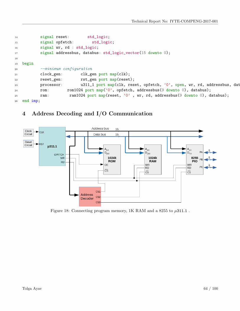
Technical Report No: IYTE-COMPENG-2017-001
14 signal reset: std_logic;
15 signal opfetch: std_logic;
16 signal wr, rd : std_logic;
17 signal addressbus, databus: std_logic_vector(15 downto 0);
18
19 begin
20 --minimum configuration
21 clock_gen: clk_gen port map(clk);
22 reset_gen: rst_gen port map(reset);
23 processor: u311_1 port map(clk, reset, opfetch, ’0’, open, wr, rd, addressbus, databus);
24 rom: rom1024 port map(’0’, opfetch, addressbus(9 downto 0), databus);
25 ram: ram1024 port map(reset, ’0’ , wr, rd, addressbus(9 downto 0), databus);
26 end imp;
4 Address Decoding and I/O Communication
Figure 18: Connecting program memory, 1K RAM and a 8255 to µ311.1 .
Tolga Ayav 64 / 100

Technical Report No: IYTE-COMPENG-2017-001
Figure 19: Connecting program memory, 1K RAM and a 8255 to µ311.1 .
5 Interrupts
µ311.1 ’s interrupt cycle consists of the following steps:
1. Interrupt signal is asserted by an external device (INT pin of the µ311.1 ).
2. µ311.1 produces an acknowledge signal at INTA pin.
3. 3-bit interrupt number is fetched from the data bus (D2−0 pins)
4. The content of PC is pushed onto the stack.
5. Execution jumps to the address of “000000000 & D2-0 & 1111” where the related interrupt serviceroutine (ISR) is located.
6. ret command returns from the ISR.
Each ISR has a predefined location in the memory. The ISR addresses are given in Table 4.
Table 4: ISR addressesInt. No D2−0 ISR address
0 000 000000000 000 1111
1 001 000000000 001 1111
2 010 000000000 010 1111
3 011 000000000 011 1111
4 100 000000000 100 1111
5 101 000000000 101 1111
6 110 000000000 110 1111
7 111 000000000 111 1111
Tolga Ayav 65 / 100

Technical Report No: IYTE-COMPENG-2017-001
Figure 20 shows an example application that uses three interrupts. These external interrupt signalsare ORed and connected to the INT pin of the processor. Note that the same interrupt signals are alsoconnected to the data bus, which constitutes the necessary interrupt number so that the processor canjump to the related ISR. Hereby, INTA is used as the output enable signal for 74’244 buffer. Figure 21shows the signal waveform of an interrupt cycle and the related interrupts used by this application.
Figure 20: Example application: Connecting 3 different interrupt sources to µ311.1 .
Int. No D2−0 ISR address
1 001 000000000 001 1111
2 010 000000000 010 1111
4 100 000000000 100 1111
Figure 21: Related ISRs.
6 Additional Instructions and Units
6.1 Watchdog Timer
Question 7 Add the circuit given in Figure 22 to µ311.1 . Discuss the function of this circuit. Whatadditional instruction(s) do you suggest to use this circuit?
6.2 Base Pointer Register
Question 8 Add two additional instructions like “mov bp,sp” and “mov sp,bp”. Make the necessarymodifications in µ311.1 such as adding a new base pointer register. Discuss the function and benefits of
Tolga Ayav 66 / 100
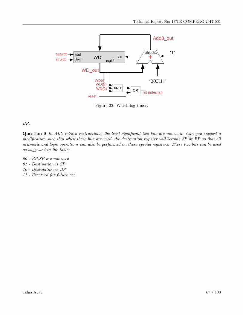
Technical Report No: IYTE-COMPENG-2017-001
Figure 22: Watchdog timer.
BP.
Question 9 In ALU-related instructions, the least significant two bits are not used. Can you suggest amodification such that when these bits are used, the destination register will become SP or BP so that allaritmetic and logic operations can also be performed on these special registers. These two bits can be usedas suggested in the table:
00 - BP,SP are not used01 - Destination is SP10 - Destination is BP11 - Reserved for future use
Tolga Ayav 67 / 100

Technical Report No: IYTE-COMPENG-2017-001
7 Programming
Figure 23: Translating from high level language to machine language.
7.1 High-Level Programming
Let’s define the following high-level imperative programming language C311.1 for µ311.1 :
S ::= x = A assignment| p = A | ∗p = A pointer assignment| x+ + | x−− increment , decrement| nop no operation| S1;S2 sequencing| if B then S1 else S2 conditional| while B do S iteration| func(vars) function call| isr0..7() interrupt service routine| uint16 x, ∗ p variable definition| register x variable definition
whereB ::= true | false | x1 x2 | not x ::= and, or
Compilation is another topic and beyond the scope of this document. Here, we will assume that acompiler can generate the intermediary assembly code given in figure 29.
Question 10 Note that Cabs is very limited language such that it is well suited to the hardware. Forexample, it supports 4 mathematical operations and only 8-bit constant values. Discuss if we could usemultiplication, i.e., op ∈ +,−, ∗. How can the compiler translate the following line to the assembly ofµ311.1 ?
t := t ∗ n;
Could we also generalize 8-bit constants to 16-bit? If so, how would you translate the following line tothe assembly of µ311.1 ?
if t! = 1024 then t := t+ 1;
Question 11 Try to develop a compiler for our Cabs language using lex and yacc tools.
Tolga Ayav 68 / 100

Technical Report No: IYTE-COMPENG-2017-001
Figure 24: A typical program memory layout 1.
7.2 Assembly and Linking
Assembly and linking are the last steps in the compilation process - they turn a list of instructionsinto an image of the program’s bits in memory. Figure 28 highlights the role of assemblers and linkersin the compilation process. This process is often hidden from us by compilation commands that doeverything required to generate an executable program. As the figure shows, most compilers do not directlygenerate machine code, but instead create the instruction-level program in the form of humanreadableassembly language. Generating assembly language rather than binary instructions frees the compilerwriter from details extraneous to the compilation process, which include the instruction format as wellas the exact addresses of instructions and data. The assembler’s job is to translate symbolic assemblylanguage statements into bit-level representations of instructions known as object code. The assemblertakes care of instruction formats and does part of the job of translating labels into addresses. However,since the program may be built from many files, the final steps in determining the addresses of instructionsand data are performed by the linker, which produces an executable binary file. That file may notnecessarily be located in the CPU’s memory, however, unless the linker happens to create the executabledirectly in RAM. The program that brings the program into memory for execution is called a loader.
Since we do not have any compiler to compile the high-level source code to the assembly format ofµ311.1 , we will do it by hand. The assembly output is seen in figure 29.
The simplest form of the assembler assumes that the starting address of the assembly language programhas been specified by the programmer. The addresses in such a program are known as absolute addresses.However, in many cases, particularly when we are creating an executable out of several component files,we do not want to specify the starting addresses for all the modules before assembly. If we did, we wouldhave to determine before assembly not only the length of each program in memory but also the order in
Tolga Ayav 69 / 100

Technical Report No: IYTE-COMPENG-2017-001
Figure 25: Example program 1.
Figure 26: Example program 2 (use of pointers).
which they would be linked into the program. Most assemblers therefore allow us to use relative addressesby specifying at the start of the file that the origin of the assembly language module is to be computedlater. Addresses within the module are then computed relative to the start of the module. The linker isthen responsible for translating relative addresses into absolute addresses.
7.3 Sample Programs
EXAMPLE1: Assume that µ311.1 is attached to 1k program memory (starting from address 0000h) and64k RAM (starting from address 0000h). Find the multiplication of two numbers stored in register A andB. The result will be placed in register C.
The assembly program is shown in Figure 30.EXAMPLE2: Find the first 30 Fibonacci numbers and place them into the RAM starting from address
0000h.The assembly program is shown in Figure 31.EXAMPLE3: Convert the C program given in Figure 32 to assembly program.The resulting assembly program is shown in Figure 33.EXAMPLE 4: µ311.1 is attached to a 256 word RAM placed at the beginning of the memory map and
Tolga Ayav 70 / 100

Technical Report No: IYTE-COMPENG-2017-001
Figure 27: Example program 3 (passing parameters to a function).
a communication device that has 2 registers placed at addresses 0140H and 0141H. I/O device sends aninterrupt to CPU when it receives data from the external world and places it into its registers. WheneverISR0 is invoked, the difference between those two registers should be computed and placed iterativelystarting from the RAMs first location. Write a C and assembly program for µ311.1 .
The resulting C program is given in Figure 34 and assembly program is given in Figure 35.
7.4 Assemblers
When translating assembly code into object code, the assembler must translate opcodes and format thebits in each instruction, and translate labels into addresses. In this section, we review the translation ofassembly language into binary. Labels make the assembly process more complex, but they are the mostimportant abstraction provided by the assembler. Labels let the programmer (a human programmer or acompiler generating assembly code) avoid worrying about the absolute locations of instructions and data.Label processing requires making two passes through the assembly source code as follows:
1. The first pass scans the code to determine the address of each label.
2. The second pass assembles the instructions using the label values computed in the first pass.
The name of each symbol and its address is stored in a symbol table that is built during the firstpass. The symbol table is built by scanning from the first instruction to the last (For the moment, weassume that we know the absolute address of the first instruction in the program). During scanning, thecurrent location in memory is kept in a program location counter (PLC). Despite the similarity in nameto a program counter, the PLC is not used to execute the program, only to assign memory locations tolabels. For example, the PLC always makes exactly one pass through the program, whereas the programcounter makes many passes over code in a loop. Thus, at the start of the first pass, the PLC is set tothe program’s starting address and the assembler looks at the first line. After examining the line, theassembler updates the PLC to the next location (since our architecture is one byte long, the PLC would
Tolga Ayav 71 / 100

Technical Report No: IYTE-COMPENG-2017-001
Figure 28: Program generation from compilation through loading.
be incremented by one) and looks at the next instruction. If the instruction begins with a label, a newentry is made in the symbol table, which includes the label name and its value. The value of the label isequal to the current value of the PLC. At the end of the first pass, the assembler rewinds to the beginningof the assembly language file to make the second pass. During the second pass, when a label name isfound, the label is looked up in the symbol table and its value substituted into the appropriate place inthe instruction. In our program, the only label L1 is replaced with “10111”.
7.5 Linking
Many assembly language programs are written as several smaller pieces rather than as a single largefile. Breaking a large program into smaller files helps delineate program modularity. If the program useslibrary routines, those will already be preassembled, and assembly language source code for the librariesmay not be available for purchase. A linker allows a program to be stitched together out of several smallerpieces. The linker operates on the object files created by the assembler and modifies the assembled codeto make the necessary links between files. Some labels will be both defined and used in the same file.Other labels will be defined in a single file but used elsewhere. The place in the file where a label is definedis known as an entry point. The place in the file where the label is used is called an external reference.The main job of the loader is to resolve external references based on available entry points. As a resultof the need to know how definitions and references connect, the assembler passes to the linker not onlythe object file but also the symbol table. Even if the entire symbol table is not kept for later debuggingpurposes, it must at least pass the entry points. External references are identified in the object code bytheir relative symbol identifiers.
The linker proceeds in two phases. First, it determines the absolute address of the start of each objectfile. The order in which object files are to be loaded is given by the user, either by specifying parameterswhen the loader is run or by creating a load map file that gives the order in which files are to be placed inmemory. Given the order in which files are to be placed in memory and the length of each object file, itis easy to compute the absolute starting address of each file. At the start of the second phase, the loadermerges all symbol tables from the object files into a single, large table. It then edits the object files tochange relative addresses into absolute addresses. This is typically performed by having the assembler
Tolga Ayav 72 / 100

Technical Report No: IYTE-COMPENG-2017-001
1 ; Example assembly program
2 .org 0x0000
3 .equ stack 0xff
4 .equ size 0x08
5 ; boot code
6 movi a, stack
7 mov sp, a
8 sub d,d,d
9 mov e,d
10 movi c, size
11 jmp _main
12
13 .org 0x000F
14 ; isr0 code
15 L: write @d,e
16 inc d
17 dec c
18 jnz L
19 ret
20
21 _main: mov h,d
22 movi g,0xAA
23 write @g,h
24 jmp _main
25 halt
Figure 29: Example assembly program for µ311.1 .
write extra bits into the object file to identify the instructions and fields that refer to labels. If a labelcannot be found in the merged symbol table, it is undefined and an error message is sent to the user.
Question 12 VHDL synthesizer sometimes produces an error like “...all logic was removed from thedesign...”. What does it mean?
Question 13 Simulate the example program in Modelsim. How many clock cycles does it take forµ311.1 to execute this program?
Tolga Ayav 73 / 100

Technical Report No: IYTE-COMPENG-2017-001
1 .org 0x0000
2 sub c,c,c
3 L: add c,c,a
4 dec b
5 jnz L
6 halt
Figure 30: Example assembly program 1 for µ311.1 .
1 .org 0x0000
2 movi a,0x00
3 movi b,0x01
4 movi c,0x02
5 movi e,0x1e
6 movi g,0xff
7 write @a,b
8 inc a
9 write @a,c
10 inc a
11 L: add f,b,c
12 write @a,f
13 inc a
14 not g
15 jz L3
16 mov b,f
17 L2: dec e
18 jnz L
19 halt
20 L3: mov c,f
21 jmp L2
Figure 31: Example assembly program 2 for µ311.1 .
Tolga Ayav 74 / 100

Technical Report No: IYTE-COMPENG-2017-001
1 uint16 clear(uint16 *x, uint16 size)
2
3 register i=0;
4 while(size--) *(x+i++)=0;
5
6 main()
7
8 clear(0,10);
9
Figure 32: C program 3 for µ311.1 .
1 .org 0x0000
2 movi h,0xff
3 mov sp,h
4 movi a,0x00
5 push a
6 movi a,0x0A
7 push a
8 call clear
9 pop a
10 pop a
11 halt
12 clear: mov b,sp
13 inc b
14 inc b
15 read c,@b
16 inc b
17 read d,@b
18 movi e,0x00
19 L: write @c,e
20 inc c
21 dec d
22 jnz L
23 ret
Figure 33: Example assembly program 3 for µ311.1 .
Tolga Ayav 75 / 100

Technical Report No: IYTE-COMPENG-2017-001
1
2 uint16 *ram_ptr=0x0000;
3
4 isr0()
5
6 uint16 *io_ptr=0x0140;
7
8 *ram_ptr++ = *(io_ptr+1)-(*io_ptr);
9
10
11 main()
12
13 while(1);
14
Figure 34: C program 4 for µ311.1 .
1 .org 0x0000
2
3 ; sp initialization. sp=0x00ff
4 movi a,ffh
5 mov sp,a
6
7 ; initialize register b as a pointer to RAM. b=0x0000
8 sub b,b,b
9
10 ; main function
11 main: jmp main
12
13 ;interrupt service routine
14 .org 0x000f
15 movi d, 0xa0
16 sl d ; d=0x0140
17 read e,@d
18 inc d
19 read f,@d
20 sub a,f,e
21 write @b,a
22 inc b
23 ret
Figure 35: Example assembly program 4 for µ311.1 .
Tolga Ayav 76 / 100

Technical Report No: IYTE-COMPENG-2017-001
1 ; Example assembly program
2 .org 0x0000
3 .equ stack 0xff
4 .equ size 0x08
5 ; boot code
6 movi a, stack
7 mov sp, a
8 sub d,d,d
9 mov e,d
10 movi c, size
11 jmp _main
12
13 .org 0x000F
14 ; isr0 code
15 L: write @d,e
16 inc d
17 dec c
18 jnz L
19 ret
20
21 _main: mov h,d
22 movi g,0xAA
23 write @g,h
24 jmp _main
25 halt
−→
Name Value
stack 0xff
size 0x08
L 15
main 20
Figure 36: Assembling (First Pass) Generating symbol table.
Tolga Ayav 77 / 100

Technical Report No: IYTE-COMPENG-2017-001
1 input line [address]:machine code
2 ------------------- -------------------------
3 ; Example assembly program
4 .org 0x0000
5 .equ stack 0xff
6 .equ size 0x08
7 ; boot code
8 movi a stack
9 [0]: 1011000011111111
10 mov sp a
11 [1]: 1011100000000000
12 sub d d d
13 [2]: 0001001101101100
14 mov e d
15 [3]: 0000010001100000
16 movi c size
17 [4]: 1011001000001000
18 jmp _main
19 [5]: 0101100000001110
20 .org 0x000F
21 ; isr0 code
22 L write @d e
23 [15]: 1010000001110000
24 inc d
25 [16]: 0011001101100000
26 dec c
27 [17]: 0011101001000000
28 jnz L
29 [18]: 0110111000000100
30 ret
31 [19]: 0111100000000000
32
33 _main mov h d
34 [20]: 0000011101100000
35 movi g 0xAA
36 [21]: 1011011010101010
37 write @g h
38 [22]: 1010000010111100
39 jmp _main
40 [23]: 0101110000000011
41 halt
42 [24]: 1000100000000000
1 b0ff
2 b800
3 136c
4 0460
5 b208
6 580e
7 0000
8 0000
9 0000
10 0000
11 0000
12 0000
13 0000
14 0000
15 0000
16 a070
17 3360
18 3a40
19 6c04
20 7800
21 0760
22 b6aa
23 a0dc
24 5c04
25 8800
Figure 37: Assembling (Second Pass) Generating object code. The left box shows the output of theassembler. The right box shows the .hex output file that can be directly placed in the program memory.
Tolga Ayav 78 / 100

Technical Report No: IYTE-COMPENG-2017-001
8 Instruction Pipelining
Pipelining, a standard feature in RISC processors, is much like an assembly line. Because the processorworks on different steps of the instruction at the same time, more instructions can be executed in a shorterperiod of time.
A useful method of demonstrating this is the laundry analogy. Let’s say that there are four loads ofdirty laundry that need to be washed, dried, and folded. We could put the the first load in the washerfor 30 minutes, dry it for 40 minutes, and then take 20 minutes to fold the clothes. Then pick up thesecond load and wash, dry, and fold, and repeat for the third and fourth loads. Supposing we started at6 PM and worked as efficiently as possible, we would still be doing laundry until midnight. However, asmarter approach to the problem would be to put the second load of dirty laundry into the washer afterthe first was already clean and whirling happily in the dryer. Then, while the first load was being folded,the second load would dry, and a third load could be added to the pipeline of laundry. Using this method,the laundry would be finished by 9:30.
µ311.1 ’s execution consists of 3 stages: fetch, decode and execution cycle. At first glance, a pipelin-ing in µ311.1 would have this form: To apply pipelining to µ311.1 , we may need additional registers.
Figure 38: Pipelining in µ311.1 .
µ311.1 has single-cycle operations and this makes pipelining easier. The only command that may com-plicate pipelining is jnz. If a jump occurs during the execution of jnz, then pipelining mechanism musttake into account this and start to fetch from the new location.
Question 14 Modify µ311.1 architecture to perform pipelining (we can call the modified microprocessoras µPabs). Reconstruct the next-state table of the control unit given in 3. Modify the VHDL codes andsimulate µPabs) in Modelsim. Please notice the execution time difference.
Question 15 For µ311.1 , find out a formula to calculate the execution time of any given program.
Question 16 Is it possible to perform context switching in µ311.1 ?
Tolga Ayav 79 / 100

Technical Report No: IYTE-COMPENG-2017-001
References
[Hwa04] Enoch O. Hwang, Digital logic and microprocessor design with vhdl, 2004.
Tolga Ayav 80 / 100

Technical Report No: IYTE-COMPENG-2017-001
Index
address decoding, 47ALU, 24, 25assembly, 52
bidirectional buffer, 23BNF for VHDL, 62buffer, 23bus communication, 47bus cycles, 36
clock, 3control unit, 34
datapath, 17
hierarchical design, 70
I/O, 47instruction register, 19instruction set, 10internal diagram of µ311.1 , 71interrupt, 48interrupt cycle, 38, 48
linking, 52
memory read cycle, 37memory write cycle, 38microprocessor, 34multiplexer, 21
nonvolatile memory, 5
opcode, 10opcode fetch cycle, 37operation code, 10
program counter, 18program memory, 5programming, 51
RAM, 7register, 18register file, 20reset, 3ROM, 5
schematic, 71stack, 34stack pointer, 19structural design, 70
testbench, 46
unidirectional buffer, 23
VHDL, 62volatile memory, 7
Tolga Ayav 81 / 100

Technical Report No: IYTE-COMPENG-2017-001
Tolga Ayav 82 / 100

Technical Report No: IYTE-COMPENG-2017-001
A Simulation in ModelSim PE Student Edition
0000
0001
00
02
0003
3000
31
20
0A
04
880
0
s_str
ts_ftch
s_...
s...
s_in
cs_ftch
s_
...
s...
s_in
cs_ft
ch
s_...
s...
s_a
dd
s_
ftch
s_..
.s..
.s_
halt
0000
0001
00
02
0003
00
04
0000
3000
31
20
0A
04
88
00
0000
01
20
01
0
01
0
0000
0000
00
01
3000
31
20
0A
04
00
01
880
0
0000
0001
0000
000
1
0000
000
2
XX
XX
0 p
s2
000000 p
s4000000 p
s6
0000
00 p
s
clk
reset
op
fetc
h
wr
rd
addre
ssbus
0000
0001
00
02
0003
da
tab
us
3000
31
20
0A
04
880
0
sta
tes_str
ts_ftch
s_...
s...
s_in
cs_ftch
s_
...
s...
s_in
cs_ft
ch
s_...
s...
s_a
dd
s_
ftch
s_..
.s..
.s_
halt
q0000
0001
00
02
0003
00
04
q0000
3000
31
20
0A
04
88
00
q0000
we
WA
01
20
rbe
rae
RA
A0
10
RB
A0
10
port
A0000
0000
00
01
port
B3000
31
20
0A
04
00
01
880
0
RF
(0)
0000
0001
RF
(1)
0000
000
1
RF
(2)
0000
000
2
RA
M(2
55
)X
XX
X
Entity
:te
stb
ench A
rchitectu
re:im
p D
ate
: T
ue D
ec 1
9 0
9:5
6:4
8 P
M +
03
2017 R
ow
: 1
Page: 1
Tolga Ayav 83 / 100

Technical Report No: IYTE-COMPENG-2017-001
B BNF Syntax for VHDL
1 abstract_literal ::= decimal_literal | based_literal
2
3 access_type_definition ::= access subtype_indication
4
5 actual_designator ::=
6 expression
7 | signal_name
8 | variable_name
9 | file_name
10 | open
11
12 actual_parameter_part ::= parameter_association_list
13
14 actual_part ::=
15 actual_designator
16 | function_name ( actual_designator )
17 | type_mark ( actual_designator )
18
19 adding_operator ::= + | - | &
20
21 aggregate ::=
22 ( element_association , element_association )
23
24 alias_declaration ::=
25 alias alias_designator [ : subtype_indication ] is name
26 [ signature ] ;
27
28 alias_designator ::= identifier | character_literal |
29 operator_symbol
30
31 allocator ::=
32 new subtype_indication
33 | new qualified_expression
34
35 architecture_body ::=
36 architecture identifier of entity_name is
37 architecture_declarative_part
38 begin
39 architecture_statement_part
40 end [ architecture ] [ architecture_simple_name ] ;
41
42 architecture_declarative_part ::=
43 block_declarative_item
44
45 architecture_statement_part ::=
46 concurrent_statement
47
48 array_type_definition ::=
49 unconstrained_array_definition |
50 constrained_array_definition
51
52 assertion ::=
53 assert condition
54 [ report expression ]
55 [ severity expression ]
56
57 assertion_statement ::= [ label : ] assertion ;
58
59 association_element ::=
60 [ formal_part => ] actual_part
61
62 association_list ::=
63 association_element , association_element
64
65 attribute_declaration ::=
66 attribute identifier : type_mark ;
67
68 attribute_designator ::= attribute_simple_name
69
70 attribute_name ::=
71 prefix [ signature ] ’ attribute_designator [ ( expression ) ]
72
73 attribute_specification ::=
74 attribute attribute_designator of
75 entity_specification is expression ;
76
77 base ::= integer
78
79 base_specifier ::= B | O | X
80
81 base_unit_declaration ::= identifier ;
82
83 based_integer ::=
84 extended_digit [ underline ] extended_digit
85
86 based_literal ::=
87 base # based_integer [ . based_integer ] # [ exponent ]
88
89 basic_character ::=
90 basic_graphic_character | format_effector
91
92 basic_graphic_character ::=
93 upper_case_letter | digit | special_character| space_character
94
95 basic_identifier ::=
96 letter [ underline ] letter_or_digit
97
98 binding_indication ::=
99 [ use entity_aspect ]
100 [ generic_map_aspect ]
101 [ port_map_aspect ]
102
103 bit_string_literal ::= base_specifier " bit_value "
104
105 bit_value ::= extended_digit [ underline ] extended_digit
106
107 block_configuration ::=
108 for block_specification
109 use_clause
110 configuration_item
111 end for ;
112
113 block_declarative_item ::=
114 subprogram_declaration
115 | subprogram_body
116 | type_declaration
117 | subtype_declaration
118 | constant_declaration
119 | signal_declaration
120 | shared_variable_declaration
121 | file_declaration
122 | alias_declaration
123 | component_declaration
124 | attribute_declaration
Tolga Ayav 84 / 100

Technical Report No: IYTE-COMPENG-2017-001
125 | attribute_specification
126 | configuration_specification
127 | disconnection_specification
128 | use_clause
129 | group_template_declaration
130 | group_declaration
131
132 block_declarative_part ::=
133 block_declarative_item
134
135 block_header ::=
136 [ generic_clause
137 [ generic_map_aspect ; ] ]
138 [ port_clause
139 [ port_map_aspect ; ] ]
140
141 block_specification ::=
142 architecture_name
143 | block_statement_label
144 | generate_statement_label [ ( index_specification ) ]
145
146 block_statement ::=
147 block_label :
148 block [ ( guard_expression ) ] [ is ]
149 block_header
150 block_declarative_part
151 begin
152 block_statement_part
153 end block [ block_label ] ;
154
155 block_statement_part ::=
156 concurrent_statement
157
158 case_statement ::=
159 [ case_label : ]
160 case expression is
161 case_statement_alternative
162 case_statement_alternative
163 end case [ case_label ] ;
164
165 case_statement_alternative ::=
166 when choices =>
167 sequence_of_statements
168
169 character_literal ::= ’ graphic_character ’
170
171 choice ::=
172 simple_expression
173 | discrete_range
174 | element_simple_name
175 | others
176
177 choices ::= choice | choice
178
179 component_configuration ::=
180 for component_specification
181 [ binding_indication ; ]
182 [ block_configuration ]
183 end for ;
184
185 component_declaration ::=
186 component identifier [ is ]
187 [ local_generic_clause ]
188 [ local_port_clause ]
189 end component [ component_simple_name ] ;
190
191 component_instantiation_statement ::=
192 instantiation_label :
193 instantiated_unit
194 [ generic_map_aspect ]
195 [ port_map_aspect ] ;
196
197 component_specification ::=
198 instantiation_list : component_name
199
200 composite_type_definition ::=
201 array_type_definition
202 | record_type_definition
203
204 concurrent_assertion_statement ::=
205 [ label : ] [ postponed ] assertion ;
206
207 concurrent_procedure_call_statement ::=
208 [ label : ] [ postponed ] procedure_call ;
209
210 concurrent_signal_assignment_statement ::=
211 [ label : ] [ postponed ] conditional_signal_assignment
212 | [ label : ] [ postponed ] selected_signal_assignment
213
214 concurrent_statement ::=
215 block_statement
216 | process_statement
217 | concurrent_procedure_call_statement
218 | concurrent_assertion_statement
219 | concurrent_signal_assignment_statement
220 | component_instantiation_statement
221 | generate_statement
222
223 condition ::= boolean_expression
224
225 condition_clause ::= until condition
226
227 conditional_signal_assignment ::=
228 target <= options conditional_waveforms ;
229
230 conditional_waveforms ::=
231 waveform when condition else
232 waveform [ when condition ]
233
234 configuration_declaration ::=
235 configuration identifier of entity_name is
236 configuration_declarative_part
237 block_configuration
238 end [ configuration ] [ configuration_simple_name ] ;
239
240 configuration_declarative_item ::=
241 use_clause
242 | attribute_specification
243 | group_declaration
244
245 configuration_declarative_part ::=
246 configuration_declarative_item
247
248 configuration_item ::=
249 block_configuration
250 | component_configuration
251
252 configuration_specification ::=
253 for component_specification binding_indication ;
254
Tolga Ayav 85 / 100

Technical Report No: IYTE-COMPENG-2017-001
255 constant_declaration ::=
256 constant identifier_list : subtype_indication [ := expression ] ;
257
258 constrained_array_definition ::=
259 array index_constraint of element_subtype_indication
260
261 constraint ::=
262 range_constraint
263 | index_constraint
264
265 context_clause ::= context_item
266
267 context_item ::=
268 library_clause
269 | use_clause
270
271 decimal_literal ::= integer [ . integer ] [ exponent ]
272
273 declaration ::=
274 type_declaration
275 | subtype_declaration
276 | object_declaration
277 | interface_declaration
278 | alias_declaration
279 | attribute_declaration
280 | component_declaration
281 | group_template_declaration
282 | group_declaration
283 | entity_declaration
284 | configuration_declaration
285 | subprogram_declaration
286 | package_declaration
287
288 delay_mechanism ::=
289 transport
290 | [ reject time_expression ] inertial
291
292 design_file ::= design_unit design_unit
293
294 design_unit ::= context_clause library_unit
295
296 designator ::= identifier | operator_symbol
297
298 direction ::= to | downto
299
300 disconnection_specification ::=
301 disconnect guarded_signal_specification after
302 time_expression ;
303
304 discrete_range ::= discrete_subtype_indication | range
305
306 element_association ::=
307 [ choices => ] expression
308
309 element_declaration ::=
310 identifier_list : element_subtype_definition ;
311
312 element_subtype_definition ::= subtype_indication
313
314 entity_aspect ::=
315 entity entity_name [ ( architecture_identifier) ]
316 | configuration configuration_name
317 | open
318
319 entity_class ::=
320 entity | architecture | configuration
321 | procedure | function | package
322 | type | subtype | constant
323 | signal | variable | component
324 | label | literal | units
325 | group | file
326
327 entity_class_entry ::= entity_class [ <> ]
328
329 entity_class_entry_list ::=
330 entity_class_entry , entity_class_entry
331
332 entity_declaration ::=
333 entity identifier is
334 entity_header
335 entity_declarative_part
336 [ begin
337 entity_statement_part ]
338 end [ entity ] [ entity_simple_name ] ;
339
340 entity_declarative_item ::=
341 subprogram_declaration
342 | subprogram_body
343 | type_declaration
344 | subtype_declaration
345 | constant_declaration
346 | signal_declaration
347 | shared_variable_declaration
348 | file_declaration
349 | alias_declaration
350 | attribute_declaration
351 | attribute_specification
352 | disconnection_specification
353 | use_clause
354 | group_template_declaration
355 | group_declaration
356
357 entity_declarative_part ::=
358 entity_declarative_item
359
360 entity_designator ::= entity_tag [ signature ]
361
362 entity_header ::=
363 [ formal_generic_clause ]
364 [ formal_port_clause ]
365
366 entity_name_list ::=
367 entity_designator , entity_designator
368 | others
369 | all
370
371 entity_specification ::=
372 entity_name_list : entity_class
373
374 entity_statement ::=
375 concurrent_assertion_statement
376 | passive_concurrent_procedure_call_statement
377 | passive_process_statement
378
379 entity_statement_part ::=
380 entity_statement
381
382 entity_tag ::= simple_name | character_literal | operator_symbol
383
384 enumeration_literal ::= identifier | character_literal
Tolga Ayav 86 / 100

Technical Report No: IYTE-COMPENG-2017-001
385
386 enumeration_type_definition ::=
387 ( enumeration_literal , enumeration_literal )
388
389 exit_statement ::=
390 [ label : ] exit [ loop_label ] [ when condition ] ;
391
392 exponent ::= E [ + ] integer | E - integer
393
394 expression ::=
395 relation and relation
396 | relation or relation
397 | relation xor relation
398 | relation [ nand relation ]
399 | relation [ nor relation ]
400 | relation xnor relation
401
402 extended_digit ::= digit | letter
403
404 extended_identifier ::=
405 \ graphic_character graphic_character \
406
407 factor ::=
408 primary [ ** primary ]
409 | abs primary
410 | not primary
411
412 file_declaration ::=
413 file identifier_list : subtype_indication
414 file_open_information ] ;
415
416 file_logical_name ::= string_expression
417
418 file_open_information ::=
419 [ open file_open_kind_expression ] is
420 file_logical_name
421
422 file_type_definition ::=
423 file of type_mark
424
425 floating_type_definition := range_constraint
426
427 formal_designator ::=
428 generic_name
429 | port_name
430 | parameter_name
431
432 formal_parameter_list ::= parameter_interface_list
433
434 formal_part ::=
435 formal_designator
436 | function_name ( formal_designator )
437 | type_mark ( formal_designator )
438
439 full_type_declaration ::=
440 type identifier is type_definition ;
441
442 function_call ::=
443 function_name [ ( actual_parameter_part ) ]
444
445 generate_statement ::=
446 generate_label :
447 generation_scheme generate
448 [ block_declarative_item
449 begin ]
450 concurrent_statement
451 end generate [ generate_label ] ;
452
453 generation_scheme ::=
454 for generate_parameter_specification
455 | if condition
456
457 generic_clause ::=
458 generic ( generic_list ) ;
459
460 generic_list ::= generic_interface_list
461
462 generic_map_aspect ::=
463 generic map ( generic_association_list )
464
465 graphic_character ::=
466 basic_graphic_character | lower_case_letter |
467 other_special_character
468
469 group_constituent ::= name | character_literal
470
471 group_constituent_list ::= group_constituent , group_constituent
472
473 group_template_declaration ::=
474 group identifier is ( entity_class_entry_list ) ;
475
476 group_declaration ::=
477 group identifier : group_template_name ( group_constituent_list ) ;
478
479 guarded_signal_specification ::=
480 guarded_signal_list : type_mark
481
482 identifier ::=
483 basic_identifier | extended_identifier
484
485 identifier_list ::= identifier , identifier
486
487 if_statement ::=
488 [ if_label : ]
489 if condition then
490 sequence_of_statements
491 elsif condition then
492 sequence_of_statements
493 [ else
494 sequence_of_statements ]
495 end if [ if_label ] ;
496
497 incomplete_type_declaration ::= type identifier ;
498
499 index_constraint ::= ( discrete_range , discrete_range )
500
501 index_specification ::=
502 discrete_range
503 | static_expression
504
505 index_subtype_definition ::= type_mark range <>
506
507 indexed_name ::= prefix ( expression , expression )
508
509 instantiated_unit ::=
510 [ component ] component_name
511 | entity entity_name [ ( architecture_identifier ) ]
512 | configuration configuration_name
513
514 instantiation_list ::=
Tolga Ayav 87 / 100

Technical Report No: IYTE-COMPENG-2017-001
515 instantiation_label , instantiation_label
516 | others
517 | all
518
519 integer ::= digit [ underline ] digit
520
521 integer_type_definition ::= range_constraint
522
523 interface_constant_declaration ::=
524 [ constant ] identifier_list : [ in ]
525 subtype_indication [ := static_expression ]
526
527 interface_declaration ::=
528 interface_constant_declaration
529 | interface_signal_declaration
530 | interface_variable_declaration
531 | interface_file_declaration
532
533 interface_element ::= interface_declaration
534
535 interface_file_declaration ::=
536 file identifier_list : subtype_indication
537
538 interface_list ::=
539 interface_element ; interface_element
540
541 interface_signal_declaration ::=
542 [signal] identifier_list : [ mode ] subtype_indication
543 [ bus ] [ := static_expression ]
544
545 interface_variable_declaration ::=
546 [variable] identifier_list : [ mode ]
547 subtype_indication [ := static_expression ]
548
549 iteration_scheme ::=
550 while condition
551 | for loop_parameter_specification
552
553 label ::= identifier
554
555 letter ::= upper_case_letter | lower_case_letter
556
557 letter_or_digit ::= letter | digit
558
559 library_clause ::= library logical_name_list ;
560
561 library_unit ::=
562 primary_unit
563 | secondary_unit
564
565 literal ::=
566 numeric_literal
567 | enumeration_literal
568 | string_literal
569 | bit_string_literal
570 | null
571
572 logical_name ::= identifier
573
574 logical_name_list ::= logical_name , logical_name
575
576 logical_operator ::= and|or|nand|nor|xor|xnor
577
578 loop_statement ::=
579 [ loop_label : ]
580 [ iteration_scheme ] loop
581 sequence_of_statements
582 end loop [ loop_label ] ;
583
584 miscellaneous_operator ::= ** | abs | not
585
586 mode ::= in | out | inout | buffer | linkage
587
588 multiplying_operator ::= * | / | mod | rem
589
590 name ::=
591 simple_name
592 | operator_symbol
593 | selected_name
594 | indexed_name
595 | slice_name
596 | attribute_name
597
598 next_statement ::=
599 [ label : ] next [ loop_label ] [ when condition ] ;
600
601 null_statement ::= [ label : ] null ;
602
603 numeric_literal ::=
604 abstract_literal
605 | physical_literal
606
607 object_declaration ::=
608 constant_declaration
609 | signal_declaration
610 | variable_declaration
611 | file_declaration
612
613 operator_symbol ::= string_literal
614
615 options ::= [ guarded ] [ delay_mechanism ]
616
617 package_body ::=
618 package body package_simple_name is
619 package_body_declarative_part
620 end [ package body ] [ package_simple_name ] ;
621
622 package_body_declarative_item ::=
623 subprogram_declaration
624 | subprogram_body
625 | type_declaration
626 | subtype_declaration
627 | constant_declaration
628 | shared_variable_declaration
629 | file_declaration
630 | alias_declaration
631 | use_clause
632 | group_template_declaration
633 | group_declaration
634
635 package_body_declarative_part ::=
636 package_body_declarative_item
637
638 package_declaration ::=
639 package identifier is
640 package_declarative_part
641 end [ package ] [ package_simple_name ] ;
642
643 package_declarative_item ::=
644 subprogram_declaration
Tolga Ayav 88 / 100

Technical Report No: IYTE-COMPENG-2017-001
645 | type_declaration
646 | subtype_declaration
647 | constant_declaration
648 | signal_declaration
649 | shared_variable_declaration
650 | file_declaration
651 | alias_declaration
652 | component_declaration
653 | attribute_declaration
654 | attribute_specification
655 | disconnection_specification
656 | use_clause
657 | group_template_declaration
658 | group_declaration
659
660 package_declarative_part ::=
661 package_declarative_item
662
663 parameter_specification ::=
664 identifier in discrete_range
665
666 physical_literal ::= [ abstract_literal ] unit_name
667
668 physical_type_definition ::=
669 range_constraint
670 units
671 base_unit_declaration
672 secondary_unit_declaration
673 end units [ physical_type_simple_name ]
674
675 port_clause ::=
676 port ( port_list ) ;
677
678 port_list ::= port_interface_list
679
680 port_map_aspect ::=
681 port map ( port_association_list )
682
683 prefix ::=
684 name
685 | function_call
686
687 primary ::=
688 name
689 | literal
690 | aggregate
691 | function_call
692 | qualified_expression
693 | type_conversion
694 | allocator
695 | ( expression )
696
697 primary_unit ::=
698 entity_declaration
699 | configuration_declaration
700 | package_declaration
701
702 procedure_call ::= procedure_name
703 [ ( actual_parameter_part ) ]
704
705 procedure_call_statement ::=
706 [ label : ] procedure_call ;
707
708 process_declarative_item ::=
709 subprogram_declaration
710 | subprogram_body
711 | type_declaration
712 | subtype_declaration
713 | constant_declaration
714 | variable_declaration
715 | file_declaration
716 | alias_declaration
717 | attribute_declaration
718 | attribute_specification
719 | use_clause
720 | group_template_declaration
721 | group_declaration
722
723 process_declarative_part ::=
724 process_declarative_item
725
726 process_statement ::=
727 [ process_label : ]
728 [ postponed ] process [ ( sensitivity_list ) ] [ is ]
729 process_declarative_part
730 begin
731 process_statement_part
732 end [ postponed ] process [ process_label ] ;
733
734 process_statement_part ::=
735 sequential_statement
736
737 qualified_expression ::=
738 type_mark ’ ( expression )
739 | type_mark ’ aggregate
740
741 range ::=
742 range_attribute_name
743 | simple_expression direction simple_expression
744
745 range_constraint ::= range range
746
747 record_type_definition ::=
748 record
749 element_declaration
750 element_declaration
751 end record [ record_type_simple_name ]
752
753 relation ::=
754 shift_expression [ relational_operator shift_expression ]
755
756 relational_operator ::= = | /= | < | <= | > | >=
757
758 report_statement ::=
759 [ label : ]
760 report expression
761 [ severity expression ] ;
762
763 return_statement ::=
764 [ label : ] return [ expression ] ;
765
766 scalar_type_definition ::=
767 enumeration_type_definition | integer_type_definition
768 | floating_type_definition | physical_type_definition
769
770 secondary_unit ::=
771 architecture_body
772 | package_body
773
774 secondary_unit_declaration ::= identifier = physical_literal ;
Tolga Ayav 89 / 100

Technical Report No: IYTE-COMPENG-2017-001
775
776 selected_name ::= prefix . suffix
777
778 selected_signal_assignment ::=
779 with expression select
780 target <= options selected_waveforms ;
781
782 selected_waveforms ::=
783 waveform when choices ,
784 waveform when choices
785
786 sensitivity_clause ::= on sensitivity_list
787
788 sensitivity_list ::= signal_name , signal_name
789
790 sequence_of_statements ::=
791 sequential_statement
792
793 sequential_statement ::=
794 wait_statement
795 | assertion_statement
796 | report_statement
797 | signal_assignment_statement
798 | variable_assignment_statement
799 | procedure_call_statement
800 | if_statement
801 | case_statement
802 | loop_statement
803 | next_statement
804 | exit_statement
805 | return_statement
806 | null_statement
807
808 shift_expression ::=
809 simple_expression [ shift_operator simple_expression ]
810
811 shift_operator ::= sll | srl | sla | sra | rol | ror
812
813 sign ::= + | -
814
815 signal_assignment_statement ::=
816 [ label : ] target <= [ delay_mechanism ] waveform ;
817
818 signal_declaration ::=
819 signal identifier_list : subtype_indication
820 [ signal_kind ] [ := expression ] ;
821
822 signal_kind ::= register | bus
823
824 signal_list ::=
825 signal_name , signal_name
826 | others
827 | all
828
829 signature ::= [ [ type_mark , type_mark ]
830 [ return type_mark ] ]
831
832 simple_expression ::=
833 [ sign ] term adding_operator term
834
835 simple_name ::= identifier
836
837 slice_name ::= prefix ( discrete_range )
838
839 string_literal ::= " graphic_character "
840
841 subprogram_body ::=
842 subprogram_specification is
843 subprogram_declarative_part
844 begin
845 subprogram_statement_part
846 end [ subprogram_kind ] [ designator ] ;
847
848 subprogram_declaration ::=
849 subprogram_specification ;
850
851 subprogram_declarative_item ::=
852 subprogram_declaration
853 | subprogram_body
854 | type_declaration
855 | subtype_declaration
856 | constant_declaration
857 | variable_declaration
858 | file_declaration
859 | alias_declaration
860 | attribute_declaration
861 | attribute_specification
862 | use_clause
863 | group_template_declaration
864 | group_declaration
865
866 subprogram_declarative_part ::=
867 subprogram_declarative_item
868
869 subprogram_kind ::= procedure | function
870
871 subprogram_specification ::=
872 procedure designator [ ( formal_parameter_list ) ]
873 | [ pure | impure ] function designator [ ( formal_parameter_list ) ]
874 return type_mark
875
876 subprogram_statement_part ::=
877 sequential_statement
878
879 subtype_declaration ::=
880 subtype identifier is subtype_indication ;
881
882 subtype_indication ::=
883 [ resolution_function_name ] type_mark [ constraint ]
884
885 suffix ::=
886 simple_name
887 | character_literal
888 | operator_symbol
889 | all
890
891 target ::=
892 name
893 | aggregate
894
895 term ::=
896 factor multiplying_operator factor
897
898 timeout_clause ::= for time_expression
899
900 type_conversion ::= type_mark ( expression )
901
902 type_declaration ::=
903 full_type_declaration
904 | incomplete_type_declaration
Tolga Ayav 90 / 100

Technical Report No: IYTE-COMPENG-2017-001
905
906 type_definition ::=
907 scalar_type_definition
908 | composite_type_definition
909 | access_type_definition
910 | file_type_definition
911
912 type_mark ::=
913 type_name
914 | subtype_name
915
916 unconstrained_array_definition ::=
917 array ( index_subtype_definition
918 , index_subtype_definition )
919 of element_subtype_indication
920
921 use_clause ::=
922 use selected_name , selected_name ;
923
924 variable_assignment_statement ::=
925 [ label : ] target := expression ;
926
927 variable_declaration::=
928 [ shared ] variable identifier_list :
929 subtype_indication [ := expression ] ;
930
931 wait_statement ::=
932 [ label : ] wait [ sensitivity_clause ]
933 [ condition_clause ] [ timeout_clause ] ;
934
935 waveform ::=
936 waveform_element , waveform_element
937 | unaffected
938
939 waveform_element ::=
940 value_expression [ after time_expression ]
941 | null [ after time_expression ]
Tolga Ayav 91 / 100
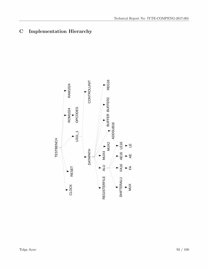
Technical Report No: IYTE-COMPENG-2017-001
C Implementation Hierarchy
Tolga Ayav 92 / 100

Technical Report No: IYTE-COMPENG-2017-001
D as311 Assembler
as311 translates assembly files to µ311.1 machine code.
1 #include <stdio.h>
2 #include <stdlib.h>
3 #include <string.h>
4 #define KNRM "\x1B[0m"
5 #define KRED "\x1B[31m"
6
7 FILE *fp=NULL,*fp2=NULL;
8 char cmd[1023][5][30];
9 unsigned pc[1023], pcnt=0;
10 unsigned cnt=0,romcnt=0;
11 unsigned base=0;
12
13 enum opcodesmov,add,sub,and,or,not,inc,dec,sr,sl,rr,jmp,jz,jnz,call,ret,nop,halt,push,pop,write,read,movi,movspr,movrsp;
14 enum registersa,b,c,d,e,f,g,h;
15
16 union
17 unsigned short int instruction; /* 16-bit instruction */
18 struct /* R type instruction */
19 int u: 2;
20 int r3: 3;
21 int r2: 3;
22 int r1: 3;
23 int opcode: 5;
24 r;
25 struct /* J type instruction */
26 int add: 10;
27 int sign: 1;
28 int opcode: 5;
29 j;
30 struct /* I type instruction */
31 int imm8: 8;
32 int r1: 3;
33 int opcode: 5;
34 i;
35 x;
36
37 int find_label(char *s,unsigned current)
38
39 int i;
40 for(i=0; i<cnt; i++)
41 if(!strcmp(cmd[i][0],s))
42
43 return pc[i]-pc[current]-1;
44
45
46 return 0;
47
48
49 int find_num(char *s)
50
51 int i;
52 for(i=0; i<cnt; i++)
53 if(!strcmp(cmd[i][1],".equ"))
54 if(!strcmp(cmd[i][2],s))
55 return strtol(cmd[i][3],NULL,16);
56
57
58
59 return strtol(s,NULL,16);
60
61
Tolga Ayav 93 / 100

Technical Report No: IYTE-COMPENG-2017-001
62 void print_binary(unsigned short k, int end, int begin)
63 int i;
64 for(i=end-1;i>=begin;i--) printf("%u",(k>>i)&0x1);
65
66
67 unsigned int assign_reg(char *s)
68
69 if(s[0]==’@’)s[0]=s[1]; s[1]=0;
70
71 if(s[0]==’s’) return 0;
72 else return s[0]-97;
73
74
75 int main(int argc, char **argv)
76
77 char s[100],s2[100];
78 char *ch=NULL;
79 unsigned char sgn=0;
80
81 int i,j,k,opr=0;
82
83 memset(cmd,0,120000);
84 memset(s,0,100);memset(s2,0,100);
85
86 if(argc<2) printf("Usage: as311 filename\n"); return 0;
87
88 if((fp=fopen(argv[1],"r"))==NULL) printf("%s cannot be opened\n",argv[1]); return 0;
89
90 // FIRST PASS //
91 while(fgets(s,100,fp))
92
93 i=j=opr=0;
94 while(*(s+i)!=0)
95 if(*(s+i)==’:’)*(s2+j)=0;j=0; strcpy(cmd[cnt][0],s2); memset(s2,0,100);
96 else if(j==0 && (*(s+i)==’ ’||*(s+i)==’\t’||*(s+i)==’\n’)) /*i++; continue;*/
97 else if(cmd[cnt][1][0]==0 && j!=0 && (*(s+i)==’ ’||*(s+i)==’,’||*(s+i)==’\n’||*(s+i)==’\t’))
98 *(s2+j)=0;j=0; strcpy(cmd[cnt][1],s2); memset(s2,0,100);
99 else if(cmd[cnt][1][0]!=0 && j!=0 && (*(s+i)==’ ’||*(s+i)==’,’||*(s+i)==’\n’))
100 *(s2+j)=0;j=0; strcpy(cmd[cnt][2+opr++],s2); if(opr==5)break; memset(s2,0,100);
101 else *(s2+j++)=*(s+i);
102 i++;
103
104 if(s[0]==’\n’) continue;
105 if(cmd[cnt][1][0]!=’.’ && cmd[cnt][1][0]!=’;’) pc[cnt]=base+pcnt++;
106 if(!strcmp(cmd[cnt][1],".org"))
107 if(strtol(cmd[cnt][2],NULL,16)>=(base+pcnt)) base=strtol(cmd[cnt][2],NULL,16);
108 else printf("Error in .org directive.\n"); return -1;
109 pcnt=0;
110
111 if(cmd[cnt][1][0]!=0)cnt++;
112 memset(s2,0,100);
113
114
115 fclose(fp); fp=fopen(strcat(strtok(argv[1],"."),".vhdl_hex"),"w");
116 fp2=fopen(strcat(strtok(argv[1],"."),".hex"),"w");
117 fprintf(fp,"constant ROM: rom_type :=(\n");
118
119 printf("input line\t\t[address]:machine code\n-------------------\t------------------------- \n");
120
121 // SECOND PASS //
122 for(i=0; i<cnt; i++)
123 x.instruction=0;
124
125 for(j=0; j<5; j++) if(cmd[i][j][0]!=0) printf("%s ",cmd[i][j]);
126
Tolga Ayav 94 / 100

Technical Report No: IYTE-COMPENG-2017-001
127 if(!strcmp(cmd[i][1],"mov") && cmd[i][2][0]==’s’)
128 x.r.opcode=movspr;x.r.r1=assign_reg(cmd[i][2]);x.r.r2=assign_reg(cmd[i][3]);
129 else if(!strcmp(cmd[i][1],"mov") && cmd[i][3][0]==’s’)
130 x.r.opcode=movrsp;x.r.r1=assign_reg(cmd[i][2]);x.r.r2=assign_reg(cmd[i][3]);
131 else if(!strcmp(cmd[i][1],"mov"))
132 x.r.opcode=mov;x.r.r1=assign_reg(cmd[i][2]);x.r.r2=assign_reg(cmd[i][3]);
133 else if(!strcmp(cmd[i][1],"add"))
134 x.r.opcode=add;x.r.r1=assign_reg(cmd[i][2]);x.r.r2=assign_reg(cmd[i][3]);x.r.r3=assign_reg(cmd[i][4]);
135 else if(!strcmp(cmd[i][1],"sub"))
136 x.r.opcode=sub;x.r.r1=assign_reg(cmd[i][2]);x.r.r2=assign_reg(cmd[i][3]);x.r.r3=assign_reg(cmd[i][4]);
137 else if(!strcmp(cmd[i][1],"and"))
138 x.r.opcode=and;x.r.r1=assign_reg(cmd[i][2]);x.r.r2=assign_reg(cmd[i][3]);x.r.r3=assign_reg(cmd[i][4]);
139 else if(!strcmp(cmd[i][1],"or"))
140 x.r.opcode=or;x.r.r1=assign_reg(cmd[i][2]);x.r.r2=assign_reg(cmd[i][3]);x.r.r3=assign_reg(cmd[i][4]);
141 else if(!strcmp(cmd[i][1],"not")) x.r.opcode=not;x.r.r1=assign_reg(cmd[i][2]);x.r.r2=assign_reg(cmd[i][2]);
142 else if(!strcmp(cmd[i][1],"inc")) x.r.opcode=inc;x.r.r1=assign_reg(cmd[i][2]);x.r.r2=assign_reg(cmd[i][2]);
143 else if(!strcmp(cmd[i][1],"dec")) x.r.opcode=dec;x.r.r1=assign_reg(cmd[i][2]);x.r.r2=assign_reg(cmd[i][2]);
144 else if(!strcmp(cmd[i][1],"sr")) x.r.opcode=sr;x.r.r1=assign_reg(cmd[i][2]);x.r.r2=assign_reg(cmd[i][2]);
145 else if(!strcmp(cmd[i][1],"sl")) x.r.opcode=sl;x.r.r1=assign_reg(cmd[i][2]);x.r.r2=assign_reg(cmd[i][2]);
146 else if(!strcmp(cmd[i][1],"rr")) x.r.opcode=rr;x.r.r1=assign_reg(cmd[i][2]);x.r.r2=assign_reg(cmd[i][2]);
147 else if(!strcmp(cmd[i][1],"jmp")) x.j.opcode=jmp;k=find_label(cmd[i][2],i); if(k<0) x.j.sign=1; x.j.add=abs(k);
148 else if(!strcmp(cmd[i][1],"jz")) x.j.opcode=jz;k=find_label(cmd[i][2],i); if(k<0) x.j.sign=1; x.j.add=abs(k);
149 else if(!strcmp(cmd[i][1],"jnz")) x.j.opcode=jnz;k=find_label(cmd[i][2],i); if(k<0) x.j.sign=1; x.j.add=abs(k);
150 else if(!strcmp(cmd[i][1],"call")) x.j.opcode=call;k=find_label(cmd[i][2],i); if(k<0) x.j.sign=1; x.j.add=abs(k);
151 else if(!strcmp(cmd[i][1],"ret")) x.j.opcode=ret;
152 else if(!strcmp(cmd[i][1],"nop")) x.j.opcode=nop;
153 else if(!strcmp(cmd[i][1],"halt")) x.j.opcode=halt;
154 else if(!strcmp(cmd[i][1],"push")) x.r.opcode=push;x.r.r3=assign_reg(cmd[i][2]);
155 else if(!strcmp(cmd[i][1],"pop")) x.r.opcode=pop;x.r.r1=assign_reg(cmd[i][2]);
156 else if(!strcmp(cmd[i][1],"write")) x.r.opcode=write;x.r.r2=assign_reg(cmd[i][2]);x.r.r3=assign_reg(cmd[i][3]);
157 else if(!strcmp(cmd[i][1],"read")) x.r.opcode=read;x.r.r1=assign_reg(cmd[i][2]);x.r.r2=assign_reg(cmd[i][3]);
158 else if(!strcmp(cmd[i][1],"movi")) x.i.opcode=movi;x.i.r1=assign_reg(cmd[i][2]);x.i.imm8=find_num(cmd[i][3]);
159
160 printf("\r\t\t\t");
161 if(cmd[i][1][0]!=’.’ && cmd[i][1][0]!=’;’)
162 printf("[%u]:\t",pc[i]);
163 printf("%s",KRED); print_binary(x.instruction,16,11);
164 printf("%s",KNRM); print_binary(x.instruction,11,0);
165
166 if(pc[i]>romcnt) for(j=0; j<(pc[i]-romcnt); j++)fprintf(fp,"X\"%.4x\",\n",0);fprintf(fp2,"%.4x\n",0);
167 romcnt=pc[i];
168 if(pc[i]==romcnt)
169 fprintf(fp,"X\"%.4x\", -- ",x.instruction);fprintf(fp2,"%.4x\n",x.instruction);
170 for(j=0; j<5; j++) if(cmd[i][j][0]!=0) fprintf(fp,"%s ",cmd[i][j]); fprintf(fp,"\n");romcnt++;
171
172
173
174 printf("\n");
175
176
177 fprintf(fp,"X\"%.4x\");\n",0);
178 fprintf(fp,"type rom_type is array(0 to %u) of cell;\n",romcnt);
179 return 1;
180
Tolga Ayav 95 / 100

Technical Report No: IYTE-COMPENG-2017-001
E Multitasking in µ311.1
Figure 39: Connecting program memory, 1K RAM and an 16-bit timer to µ311.1 .
E.1 16-bit timer
The 16-bit timer is connected to µ311.1 as an I/O device. It has two registers R0 and R1 both of whichare readable and writable. R1 is a down counter. In each clock cycle, it counts down by 1 and when itreaches to zero, R1 is reloaded with R0, generating and interrupt signal. Thus, the frequency of this timerinterrupt is determined by R0 (For example, for TCLK = 1µs and R0=10000, the interrupt period wouldbe 10ms). As seen in Figure 39, R0 and R1 are accessed at the addresses 0400h and 0401h respectively.
1 -- timer16.vhd: 16-bit timer
2
3 library ieee;
4 use ieee.std_logic_1164.all;
5 use ieee.std_logic_unsigned.all;
6 use ieee.numeric_std.all;
7
8 entity timer16 is port(
9 addr : in std_logic_vector(0 downto 0);
10 data : inout std_logic_vector(15 downto 0);
11 cs : in std_logic;
12 wr : in std_logic;
13 rd : in std_logic;
14 clk : in std_logic; -- clock.
15 int : out std_logic; -- interrupt
16 inta : in std_logic);
17 end timer16;
Tolga Ayav 96 / 100
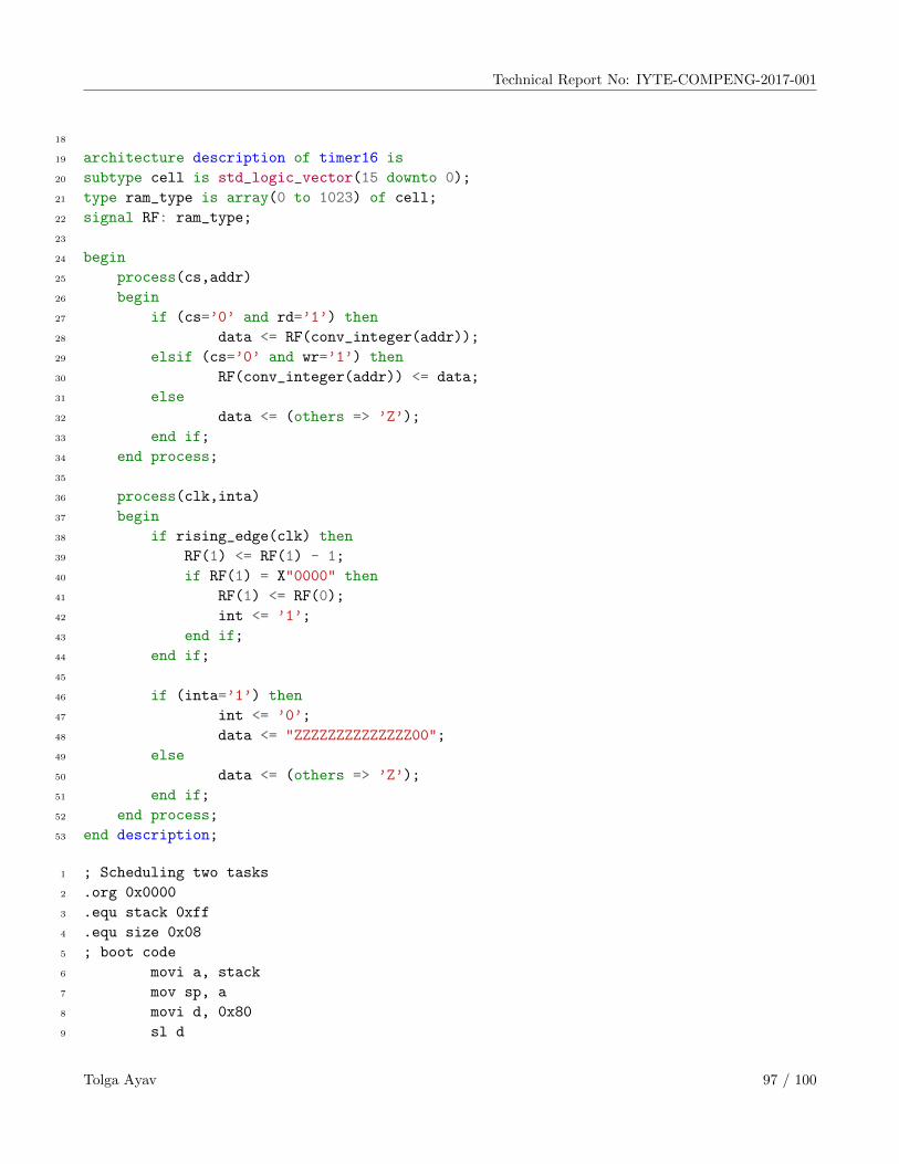
Technical Report No: IYTE-COMPENG-2017-001
18
19 architecture description of timer16 is
20 subtype cell is std_logic_vector(15 downto 0);
21 type ram_type is array(0 to 1023) of cell;
22 signal RF: ram_type;
23
24 begin
25 process(cs,addr)
26 begin
27 if (cs=’0’ and rd=’1’) then
28 data <= RF(conv_integer(addr));
29 elsif (cs=’0’ and wr=’1’) then
30 RF(conv_integer(addr)) <= data;
31 else
32 data <= (others => ’Z’);
33 end if;
34 end process;
35
36 process(clk,inta)
37 begin
38 if rising_edge(clk) then
39 RF(1) <= RF(1) - 1;
40 if RF(1) = X"0000" then
41 RF(1) <= RF(0);
42 int <= ’1’;
43 end if;
44 end if;
45
46 if (inta=’1’) then
47 int <= ’0’;
48 data <= "ZZZZZZZZZZZZZZ00";
49 else
50 data <= (others => ’Z’);
51 end if;
52 end process;
53 end description;
1 ; Scheduling two tasks
2 .org 0x0000
3 .equ stack 0xff
4 .equ size 0x08
5 ; boot code
6 movi a, stack
7 mov sp, a
8 movi d, 0x80
9 sl d
Tolga Ayav 97 / 100
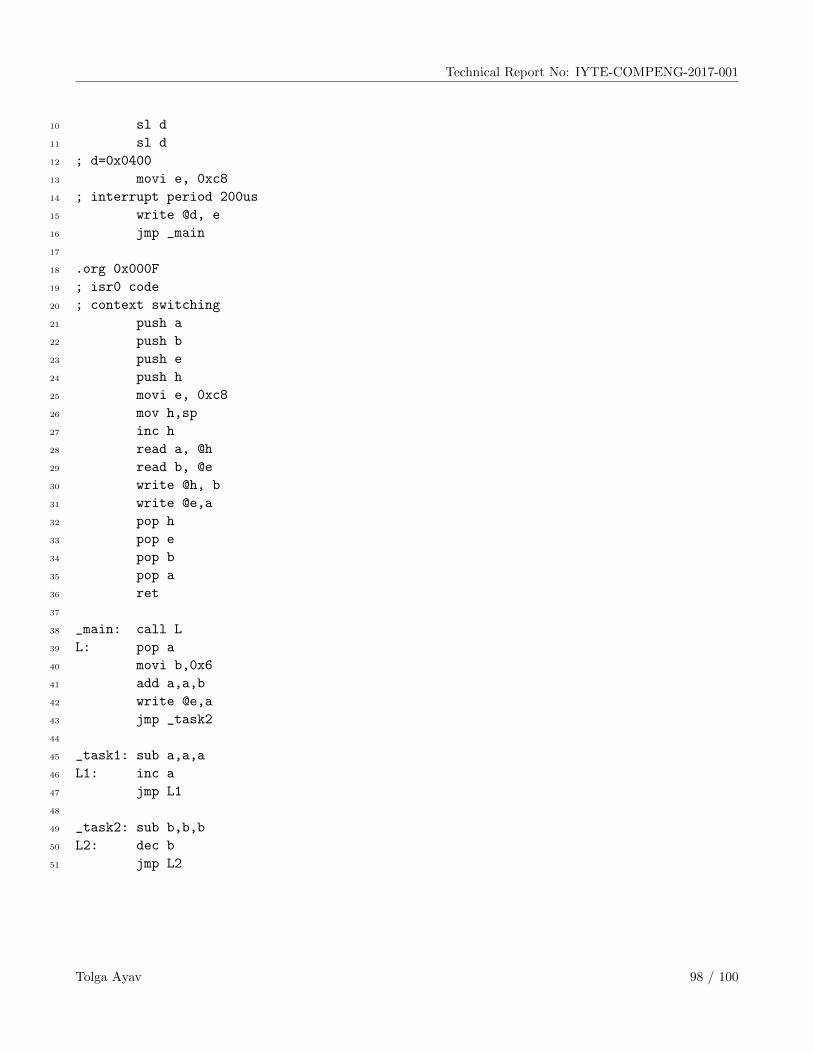
Technical Report No: IYTE-COMPENG-2017-001
10 sl d
11 sl d
12 ; d=0x0400
13 movi e, 0xc8
14 ; interrupt period 200us
15 write @d, e
16 jmp _main
17
18 .org 0x000F
19 ; isr0 code
20 ; context switching
21 push a
22 push b
23 push e
24 push h
25 movi e, 0xc8
26 mov h,sp
27 inc h
28 read a, @h
29 read b, @e
30 write @h, b
31 write @e,a
32 pop h
33 pop e
34 pop b
35 pop a
36 ret
37
38 _main: call L
39 L: pop a
40 movi b,0x6
41 add a,a,b
42 write @e,a
43 jmp _task2
44
45 _task1: sub a,a,a
46 L1: inc a
47 jmp L1
48
49 _task2: sub b,b,b
50 L2: dec b
51 jmp L2
Tolga Ayav 98 / 100

Technical Report No: IYTE-COMPENG-2017-001
F µ311.1 Internal Schematic
Tolga Ayav 99 / 100

Technical Report No: IYTE-COMPENG-2017-001
Tolga Ayav 100 / 100
Related Documents