1 Signal Integrity Testing with a Vector Network Analyzer Neil Jarvis Applications Engineer

Welcome message from author
This document is posted to help you gain knowledge. Please leave a comment to let me know what you think about it! Share it to your friends and learn new things together.
Transcript
1
Signal Integrity Testingwith a Vector Network Analyzer
Neil Jarvis
Applications Engineer

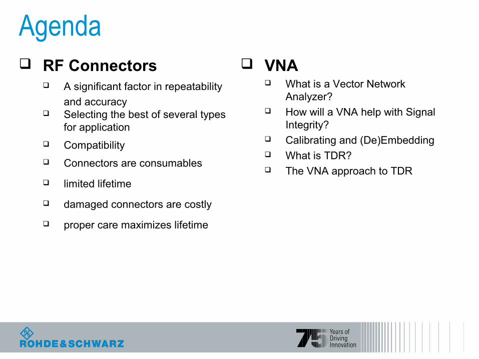
Agenda RF Connectors
A significant factor in repeatability
and accuracy Selecting the best of several types
for application
Compatibility
Connectors are consumables
limited lifetime
damaged connectors are costly
proper care maximizes lifetime
VNA What is a Vector Network
Analyzer? How will a VNA help with Signal
Integrity? Calibrating and (De)Embedding What is TDR? The VNA approach to TDR
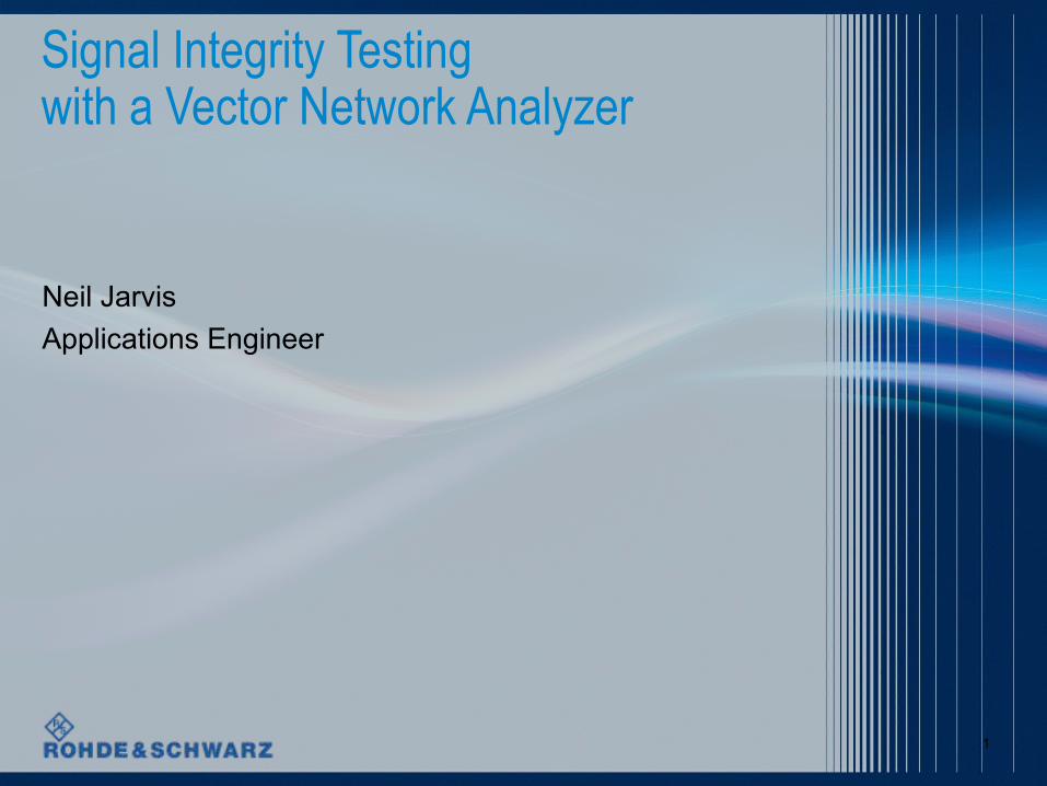
Connector Considerations
A significant factor in repeatability and accuracy Selecting the best of several types for application Compatibility Connectors are consumables
o limited lifetimeo damaged connectors are costlyo proper care maximizes lifetime
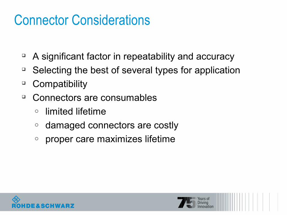
Amplitude and Phase Error from VSWR εA = 20 * log (1 ± |ΓA * ΓB|) dB
εΦ = (180 / π) *| ΓA| * |ΓB|
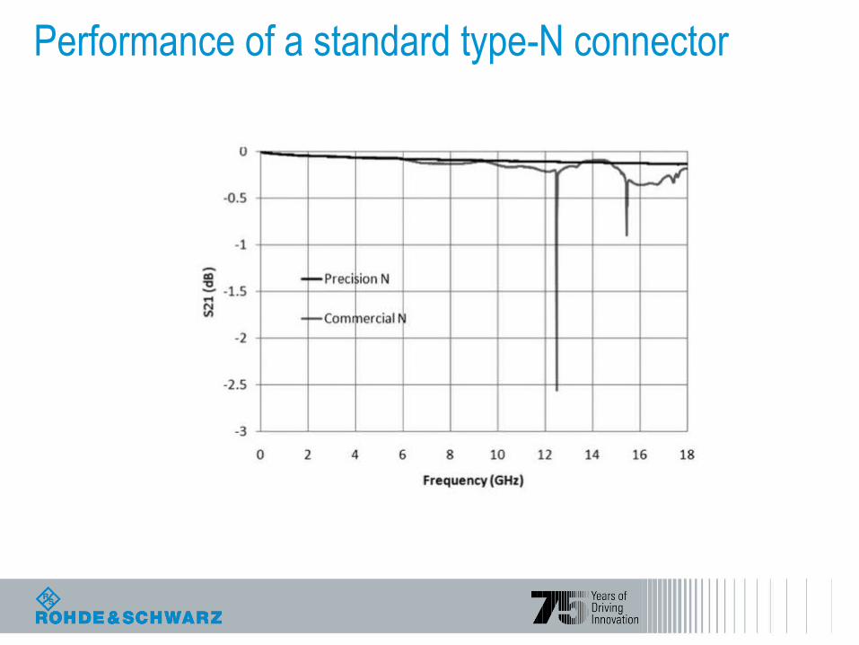
Performance of a standard type-N connector
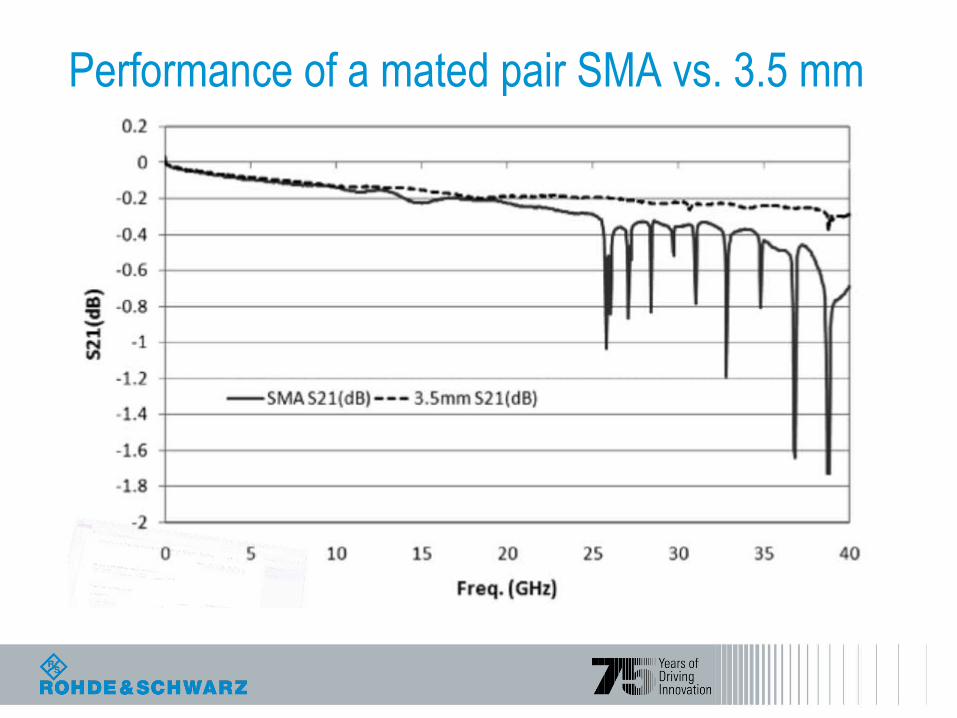
Performance of a mated pair SMA vs. 3.5 mm
-Introduction
-Detailed Views
-RF Connector Types
-Connector Grades
-Comparison of SMA and 3.5mm
-Connector Summary
-Cleaning
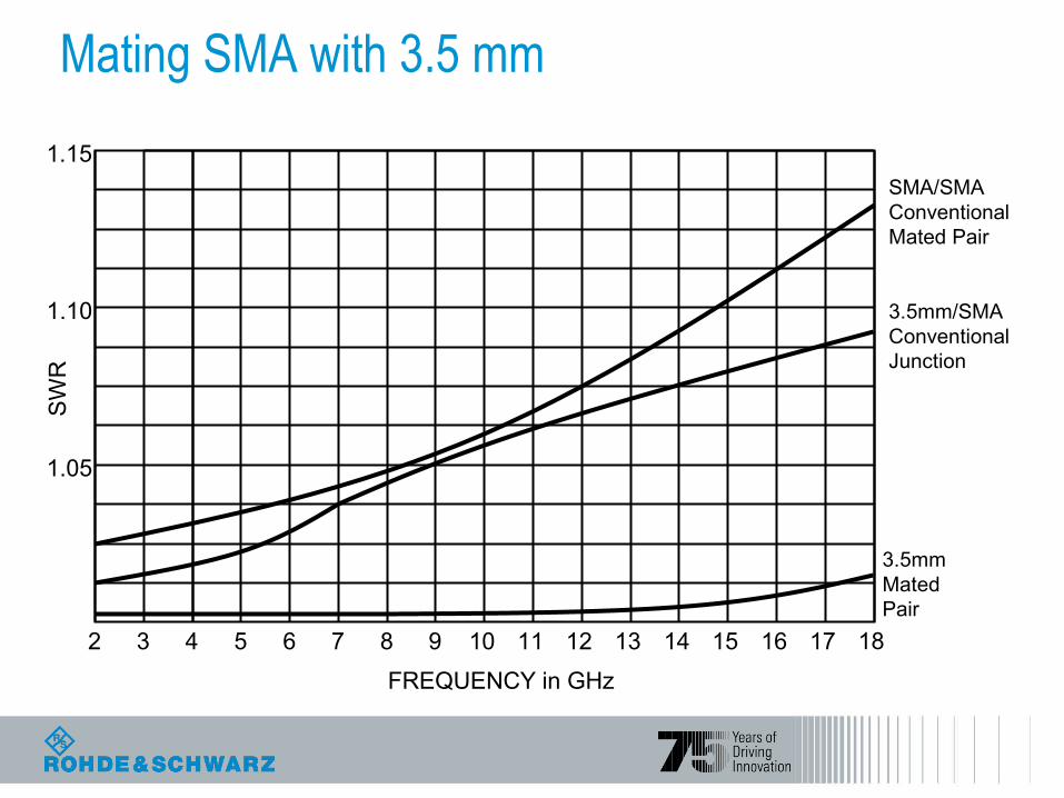
Mating SMA with 3.5 mm
SMA/SMAConventionalMated Pair
3.5mm/SMAConventionalJunction
FREQUENCY in GHz
2 3 4 5 6 7 8 9 10 11 12 13 14 15 16 17 18
1.05
1.10
1.15
SW
R
3.5mmMatedPair
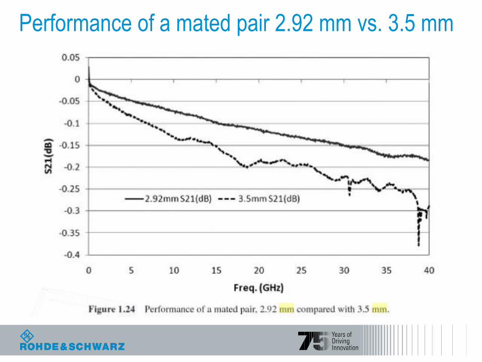
Performance of a mated pair 2.92 mm vs. 3.5 mm
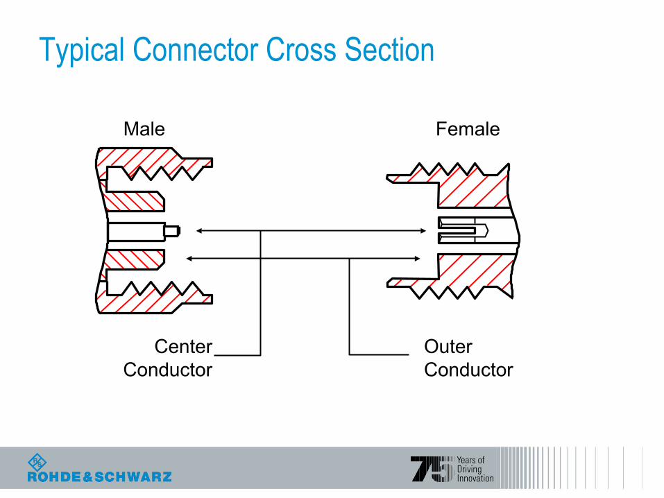
Typical Connector Cross Section
Male Female
Center Conductor
Outer Conductor
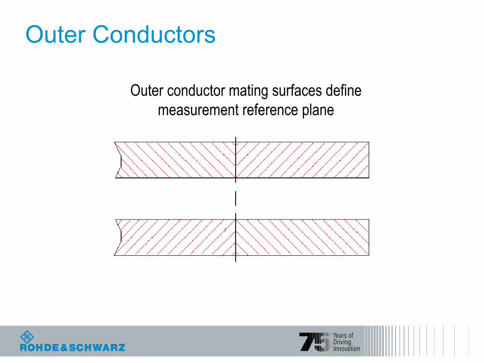
Outer Conductors
Outer conductor mating surfaces definemeasurement reference plane
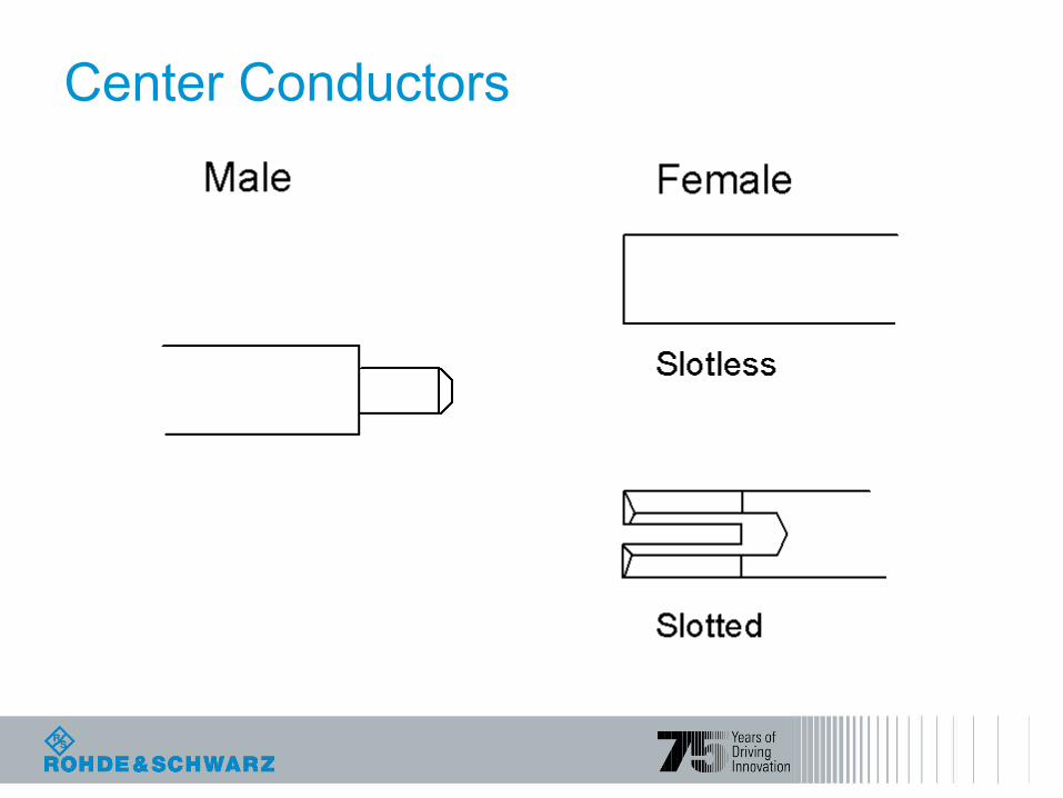
Center Conductors
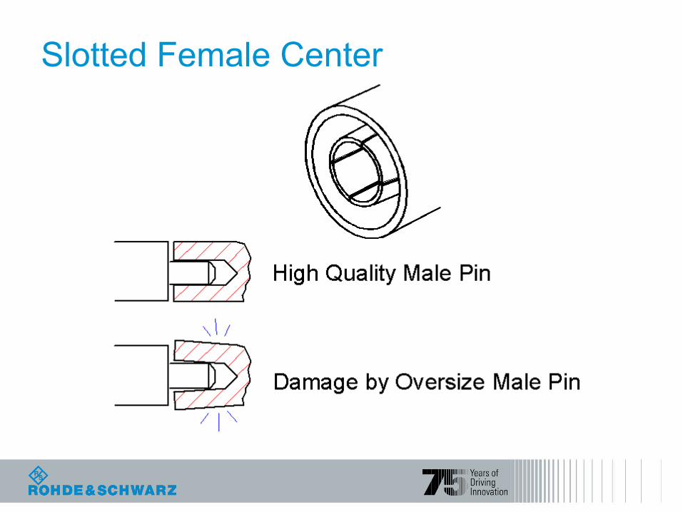
Slotted Female Center
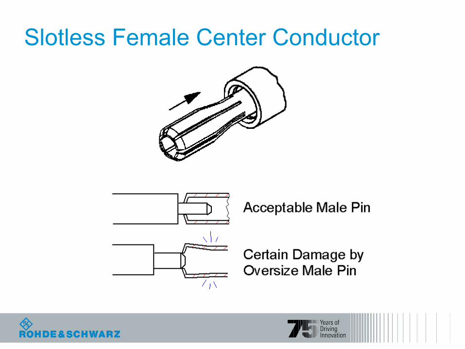
Slotless Female Center Conductor
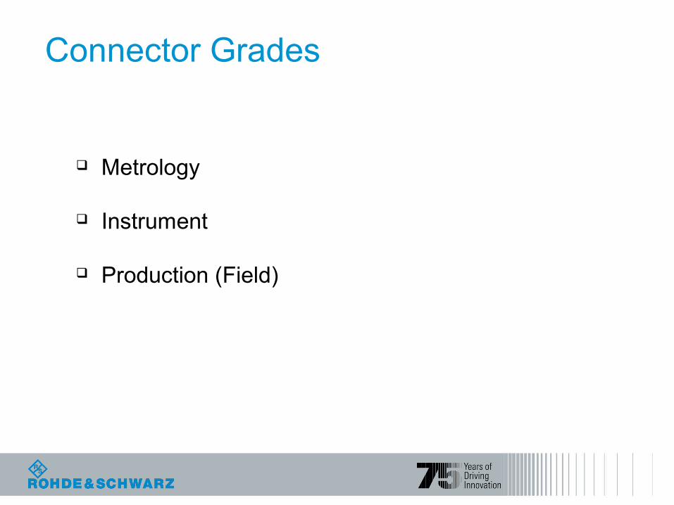
Connector Grades
Metrology
Instrument
Production (Field)
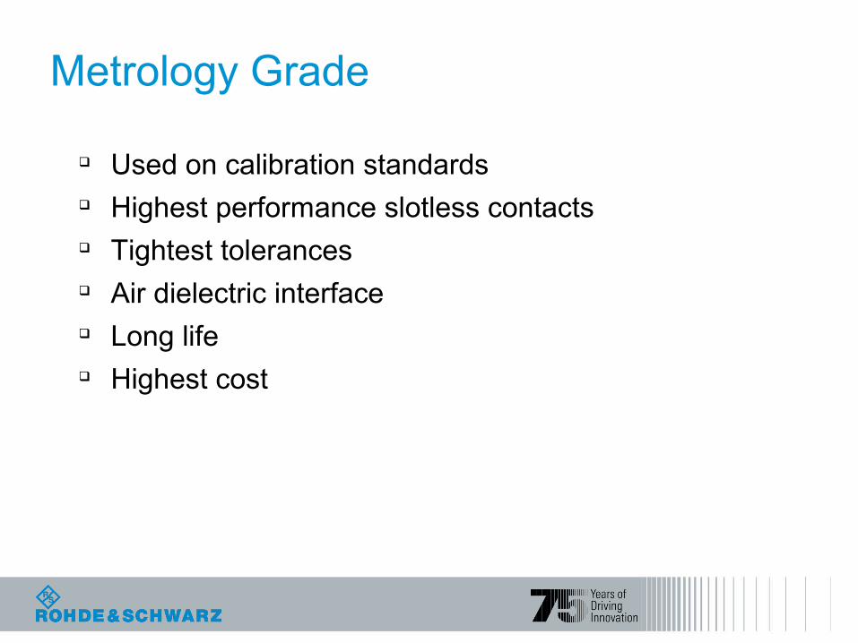
Metrology Grade
Used on calibration standards Highest performance slotless contacts Tightest tolerances Air dielectric interface Long life Highest cost
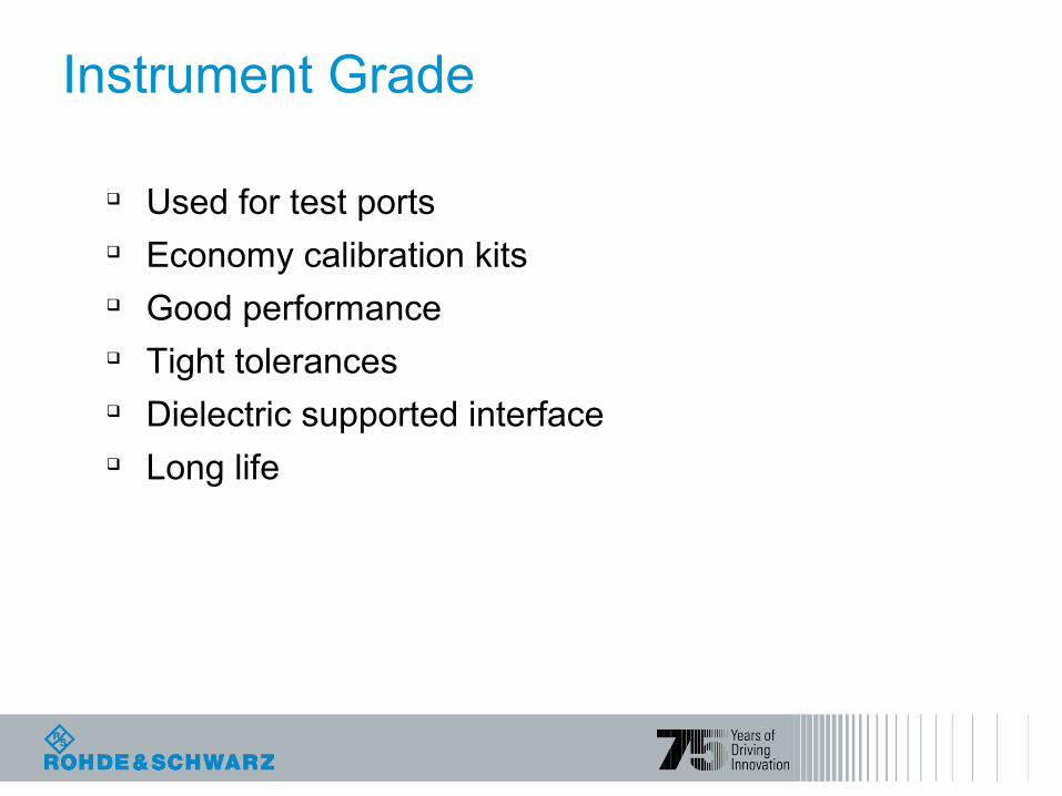
Instrument Grade
Used for test ports Economy calibration kits Good performance Tight tolerances Dielectric supported interface Long life
Production (Field) Grade
Systems and device connector Low performance Loose tolerances Dielectric supported interface Limited number of connections Lowest Cost
Always Inspect Before Connecting
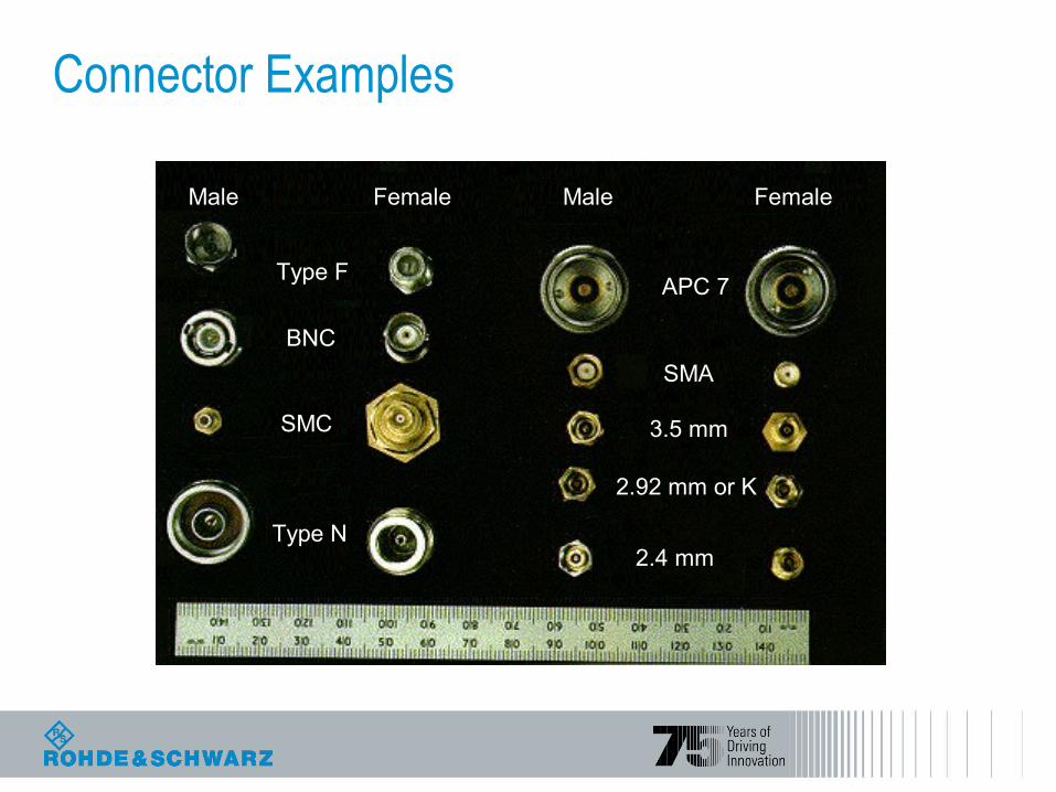
Connector Examples
Type F
BNC
SMC
Type N
APC 7
SMA
3.5 mm
2.92 mm or K
2.4 mm
MaleFemale FemaleMale
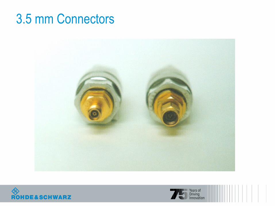
3.5 mm Connectors

dmdDA
B
C
MP
OUTER CONDUCTORMATING PLANE
A D d
C
FP
OUTER CONDUCTORMATING PLANE
3.5mm Connector Detail
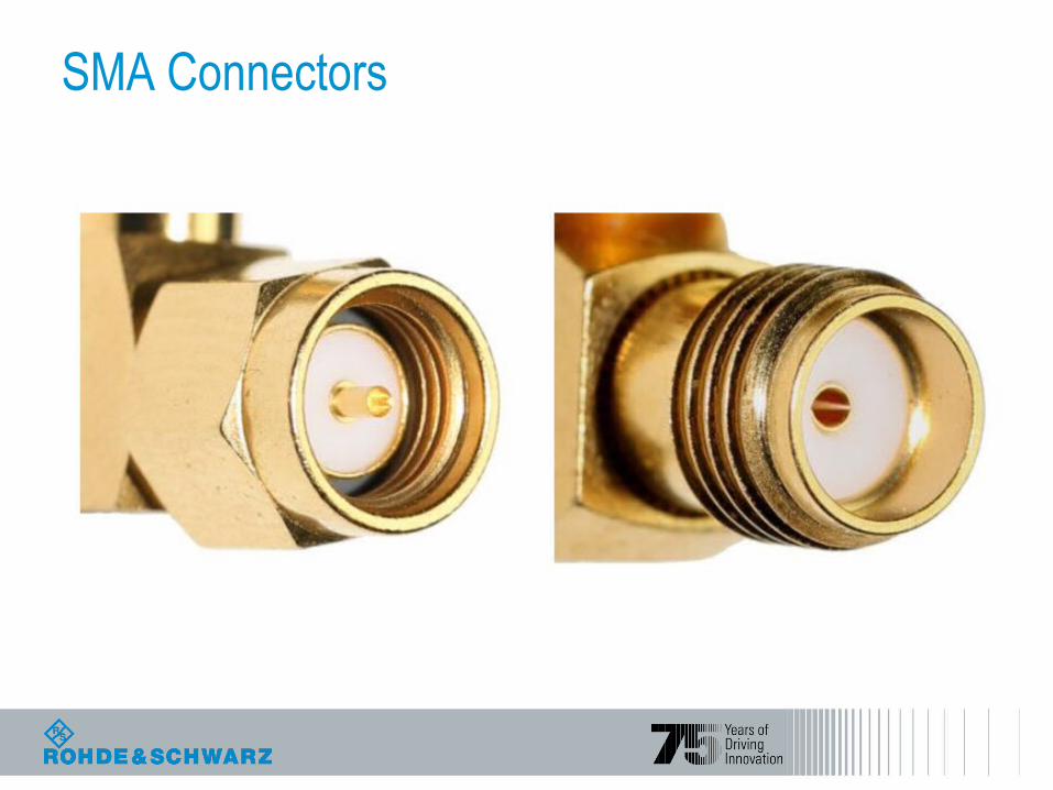
SMA Connectors
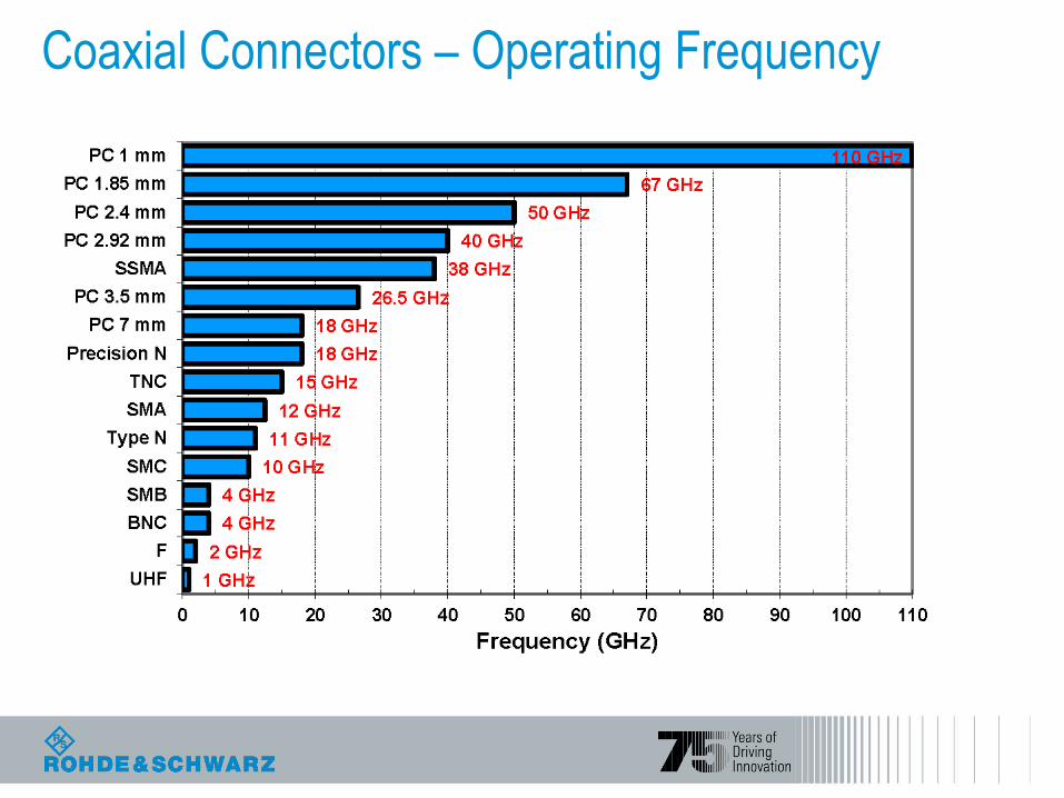
Coaxial Connectors – Operating Frequency
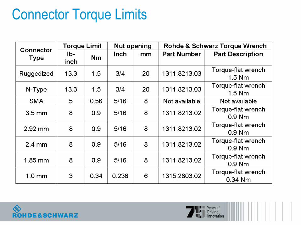
Connector Torque Limits
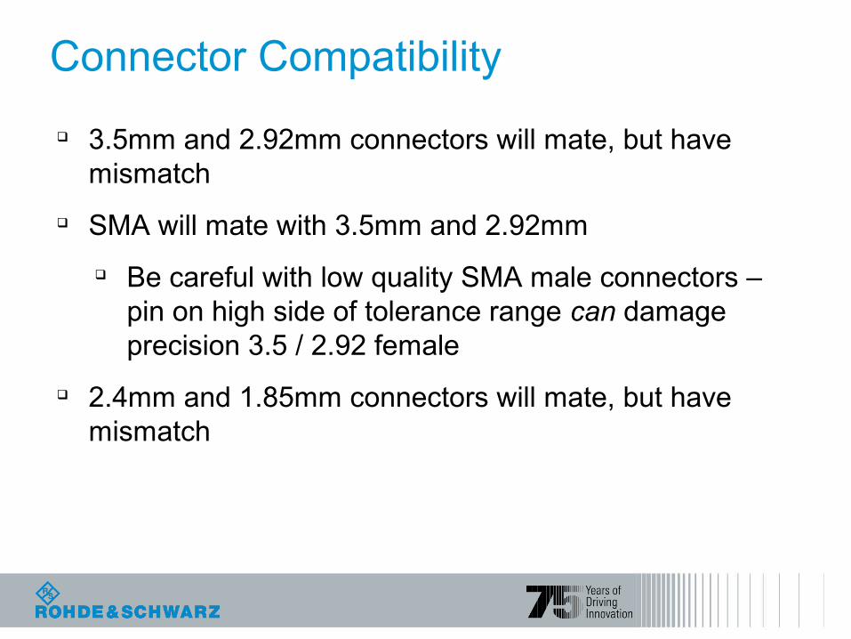
Connector Compatibility
3.5mm and 2.92mm connectors will mate, but have mismatch
SMA will mate with 3.5mm and 2.92mm
Be careful with low quality SMA male connectors – pin on high side of tolerance range can damage precision 3.5 / 2.92 female
2.4mm and 1.85mm connectors will mate, but have mismatch
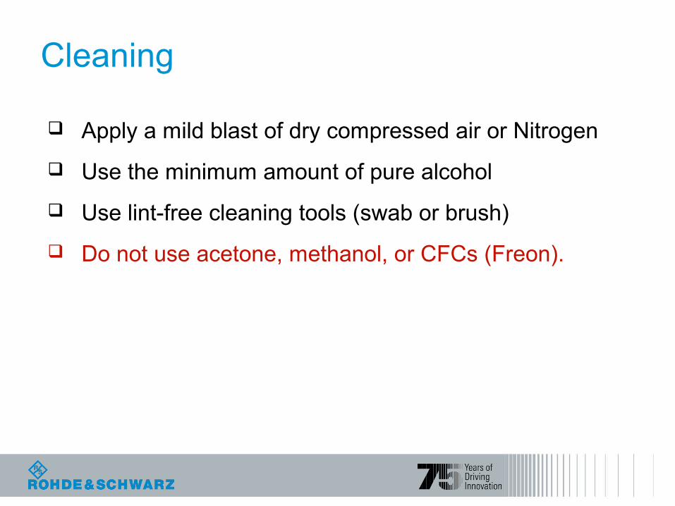
Cleaning
Apply a mild blast of dry compressed air or Nitrogen
Use the minimum amount of pure alcohol
Use lint-free cleaning tools (swab or brush)
Do not use acetone, methanol, or CFCs (Freon).
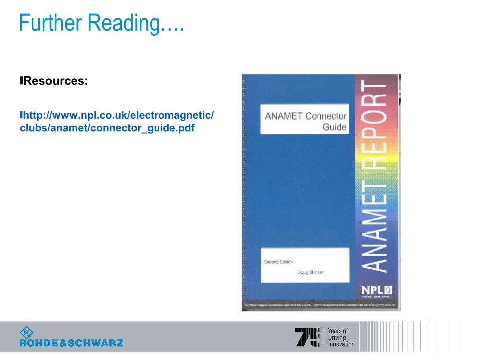
Further Reading….
lResources:
lhttp://www.npl.co.uk/electromagnetic/clubs/anamet/connector_guide.pdf
Agenda RF Connectors
A significant factor in repeatability
and accuracy Selecting the best of several types
for application
Compatibility
Connectors are consumables
limited lifetime
damaged connectors are costly
proper care maximizes lifetime
VNA What is a Vector Network
Analyzer? How will a VNA help with Signal
Integrity? Calibrating and (De)Embedding What is TDR? The VNA approach to TDR
28
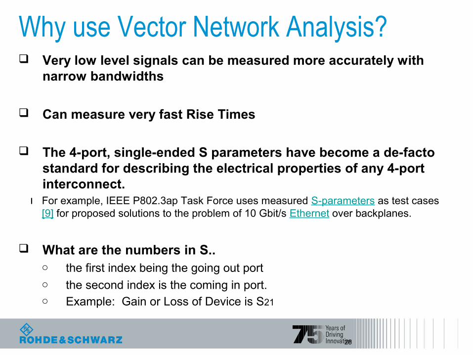
Why use Vector Network Analysis? Very low level signals can be measured more accurately with
narrow bandwidths
Can measure very fast Rise Times
The 4-port, single-ended S parameters have become a de-facto standard for describing the electrical properties of any 4-port interconnect.
ı For example, IEEE P802.3ap Task Force uses measured S-parameters as test cases[9] for proposed solutions to the problem of 10 Gbit/s Ethernet over backplanes.
What are the numbers in S.. o the first index being the going out port o the second index is the coming in port.o Example: Gain or Loss of Device is S21
29
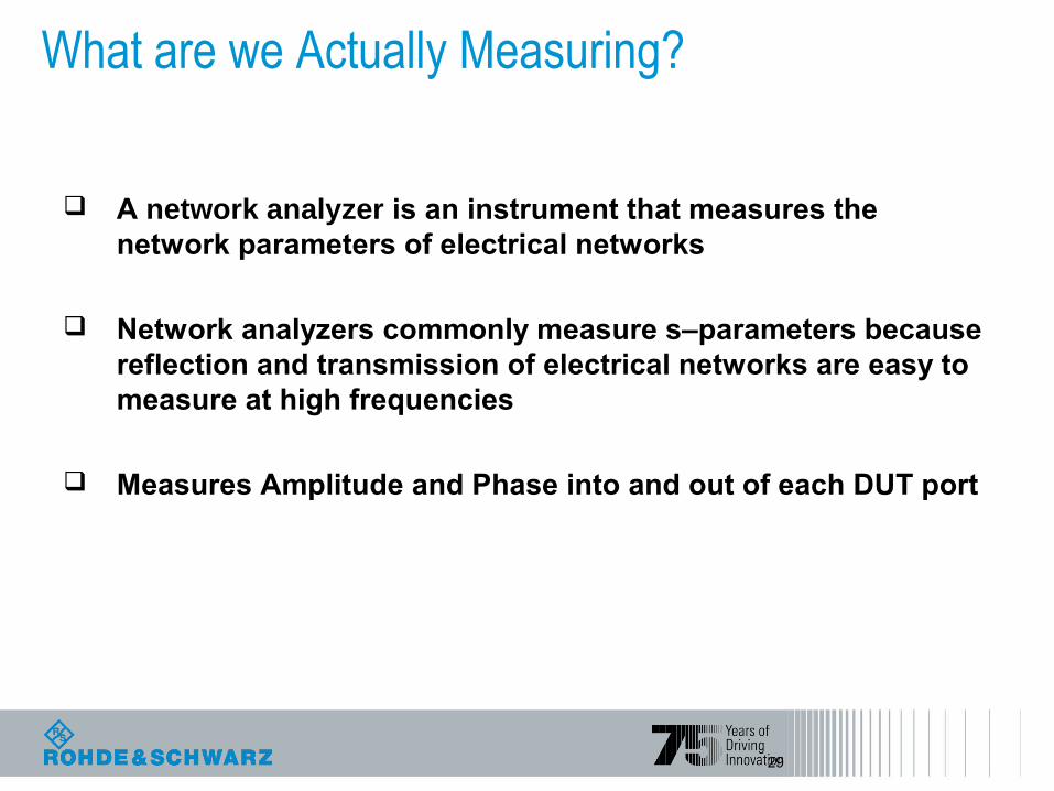
What are we Actually Measuring?
A network analyzer is an instrument that measures the network parameters of electrical networks
Network analyzers commonly measure s–parameters because reflection and transmission of electrical networks are easy to measure at high frequencies
Measures Amplitude and Phase into and out of each DUT port
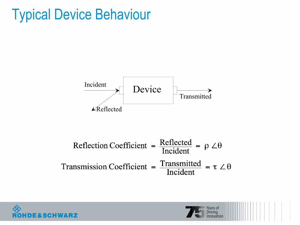
Typical Device Behaviour
DeviceIncident
Reflected
Transmitted
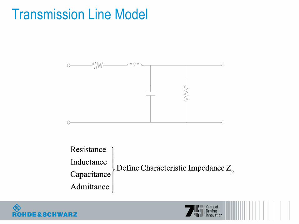
Transmission Line Model
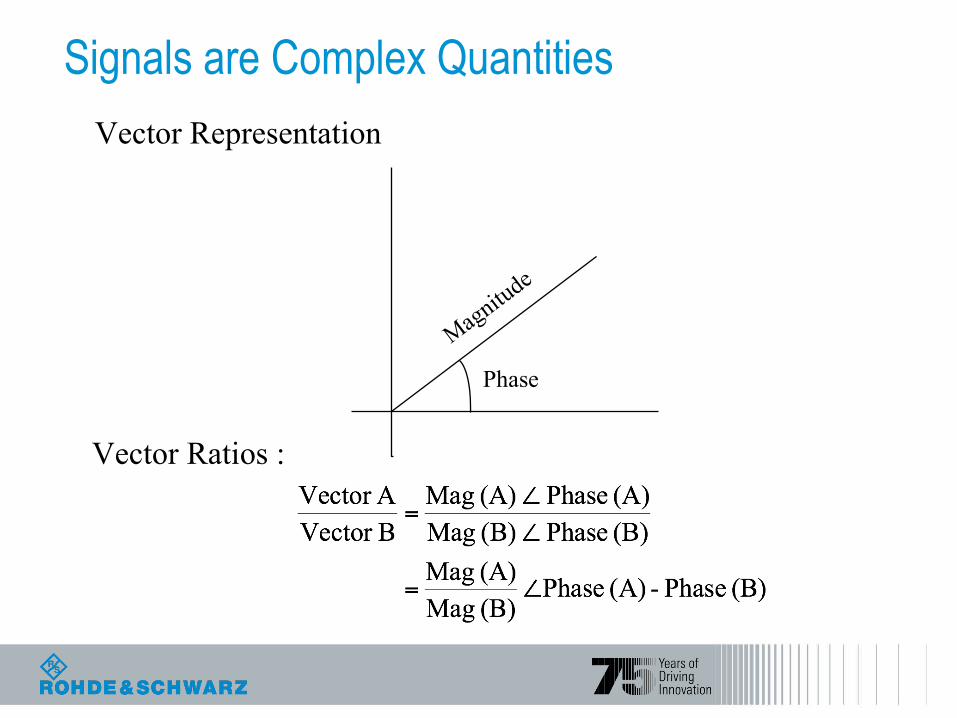
Signals are Complex Quantities
Magnitu
de
Phase
Vector Ratios :
Vector Representation

Calibration and Reference Plane
Defines Measurement Reference Linear Magnitude = 1.0 (0 dB) Phase = 0 Degrees (Reflection and Transmission)
Establishes Characteristic Impedance, Z0
Port 1 Port 2
Port 1Reference Plane
Port 2Reference Plane
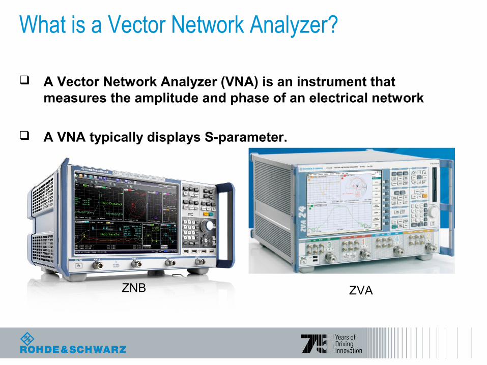
What is a Vector Network Analyzer?
A Vector Network Analyzer (VNA) is an instrument that measures the amplitude and phase of an electrical network
A VNA typically displays S-parameter.
ZNB ZVA
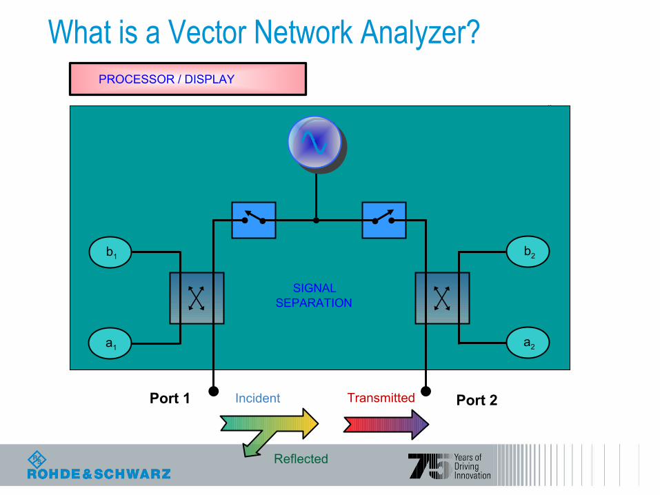
What is a Vector Network Analyzer?PROCESSOR / DISPLAY
INCIDENT (R)
Incident
Reflected
Transmitted
a1
b1
a2
b2
Port 1 Port 2
SIGNALSEPARATION
What is a Vector Network Analyzer?
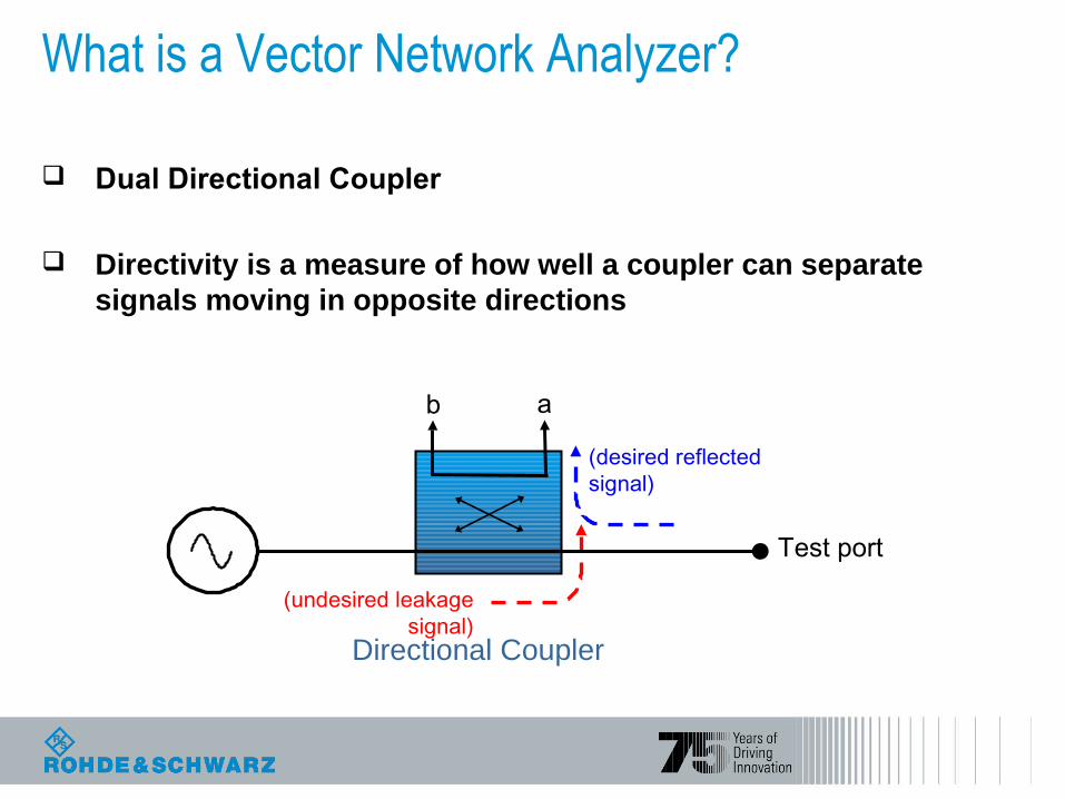
Dual Directional Coupler
Directivity is a measure of how well a coupler can separate signals moving in opposite directions
Test port
(undesired leakage signal)
(desired reflected signal)
Directional Coupler
b a
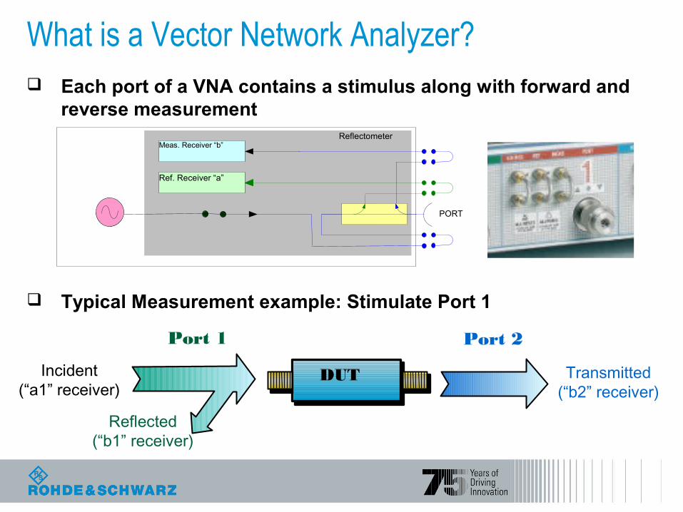
What is a Vector Network Analyzer? Each port of a VNA contains a stimulus along with forward and
reverse measurement
Typical Measurement example: Stimulate Port 1
PORT
Meas. Receiver “b”
Ref. Receiver “a”
Reflectometer
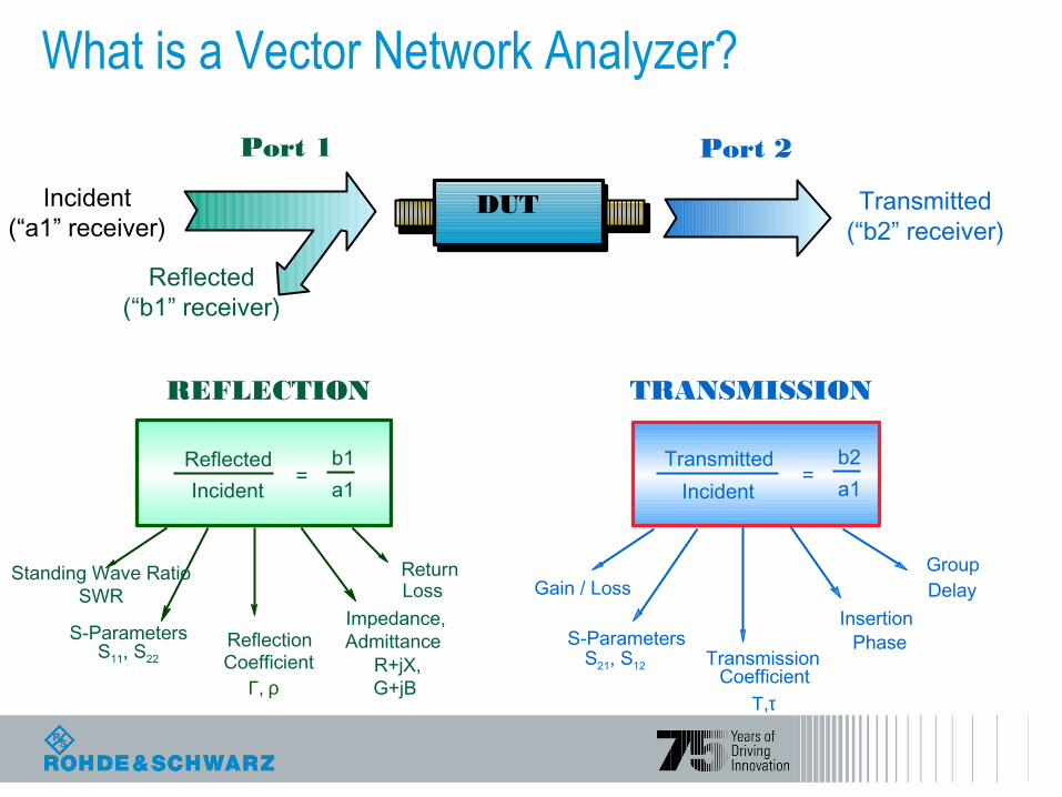
Incident(“a1” receiver)
Reflected(“b1” receiver)
Transmitted(“b2” receiver)
Port 1 Port 2
DUT

S-Parameters of a 2 port network
S11 (b1/a1)Forward reflection coefficient (input match, return loss, VSWR)
S21 (b2/a1)Forward transmission coefficient (gain or loss)
S12 (b1/a2) Reverse transmission coefficient (reverse isolation)
S22 (b2/a2)Reverse reflection coefficient (output match, return loss, VSWR)
Pin-refl
PoutPin
Prev-refl
Prev
What is a Vector Network Analyzer?
What is a Vector Network Analyzer?
TransmittedIncident
TRANSMISSION
Gain / Loss
S-ParametersS21, S12
GroupDelay
TransmissionCoefficient
Insertion Phase
ReflectedIncident
REFLECTION
Standing Wave RatioSWR
S-ParametersS11, S22
ReflectionCoefficient
Impedance, Admittance
R+jX, G+jB
ReturnLoss
Γ, ρΤ,τ
Incident(“a1” receiver)
Reflected(“b1” receiver)
Transmitted(“b2” receiver)
b1a1
=b2a1
=
Port 1 Port 2
DUT
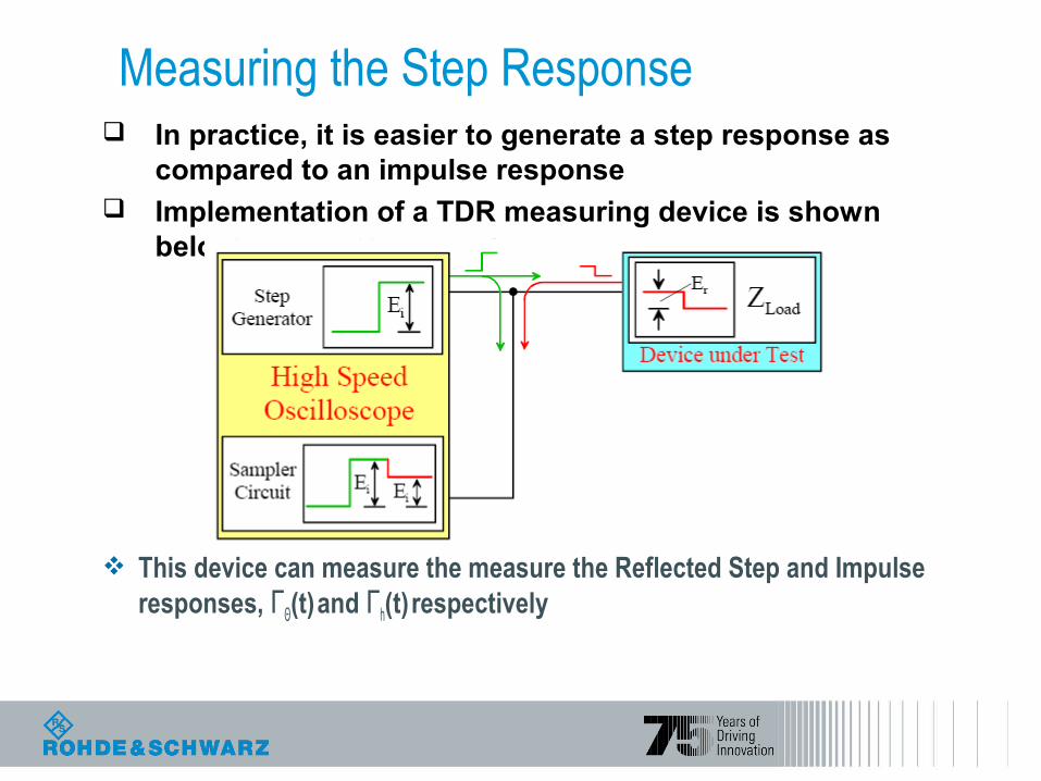
Measuring the Step Response In practice, it is easier to generate a step response as
compared to an impulse response Implementation of a TDR measuring device is shown
below:
This device can measure the measure the Reflected Step and Impulse responses, ГΘ(t) and Гh(t) respectively
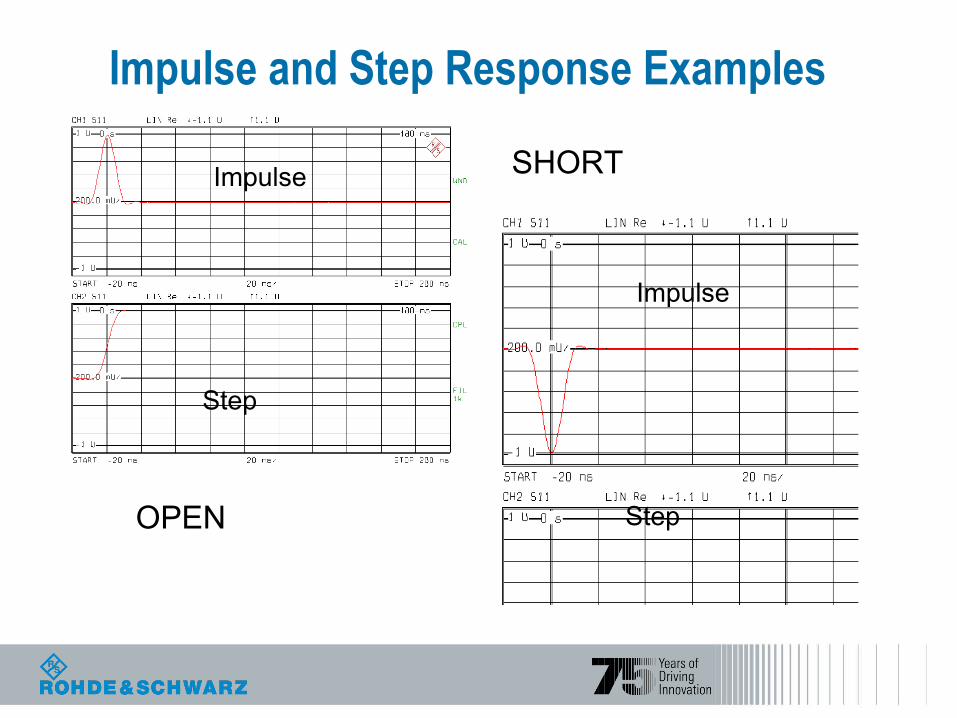
Impulse and Step Response Examples
OPEN
SHORTImpulse
Step
Impulse
Step
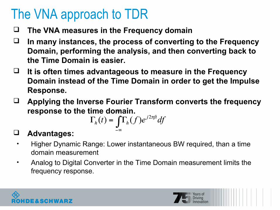
The VNA approach to TDR The VNA measures in the Frequency domain In many instances, the process of converting to the Frequency
Domain, performing the analysis, and then converting back to the Time Domain is easier.
It is often times advantageous to measure in the Frequency Domain instead of the Time Domain in order to get the Impulse Response.
Applying the Inverse Fourier Transform converts the frequency response to the time domain.
Advantages:• Higher Dynamic Range: Lower instantaneous BW required, than a time
domain measurement• Analog to Digital Converter in the Time Domain measurement limits the
frequency response.
Applications of TDR Examination of faults in transmission lines RF imaging for nondestructive evaluation Separation of echo from the wanted signal in case of
multipath propagation Moving the reference plane across unknown
irregularities

Measurements with VNAs on Cables
Classical VNA measurements S-parameters
Transmission, Reflection, cross coupling Fext, Next Group delay Electrical length
TDR measurements Fault Location Rise Time Skew (interpair and intrapair) Impedance Quality of connectors

Relationship between Frequency Domain and Time Domain
f 2f 3f 4f 5f 6f 7f freq
time
Inverse Fouriertransformation
Fouriertransformation
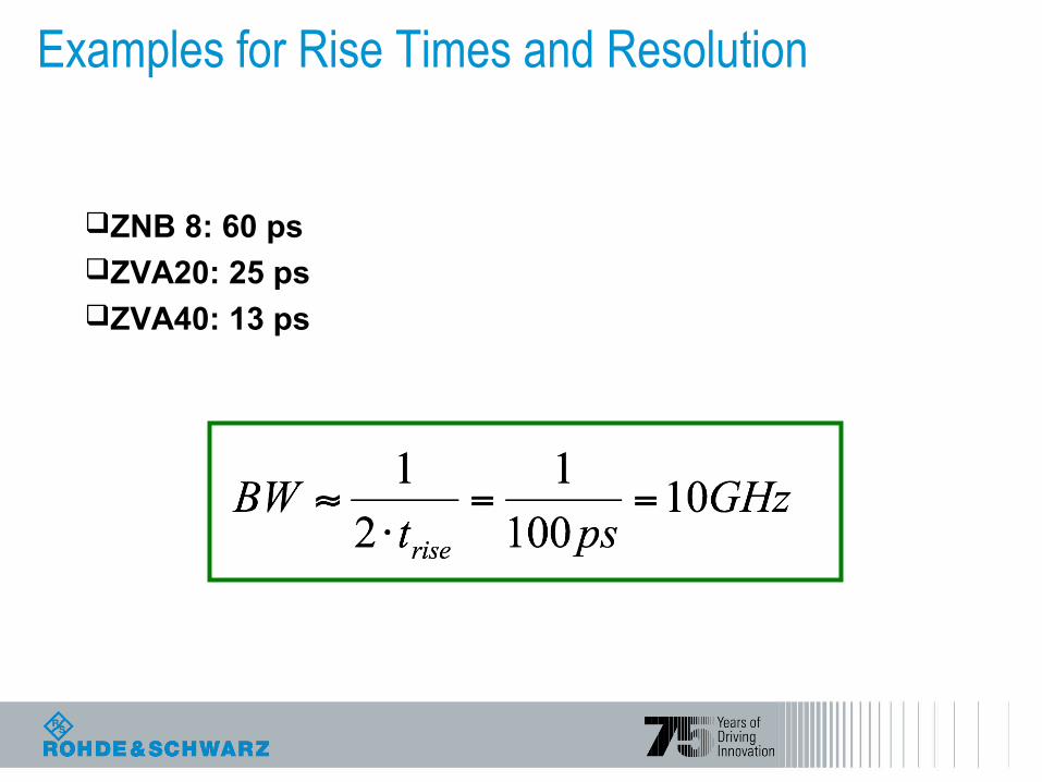
Examples for Rise Times and Resolution
ZNB 8: 60 psZVA20: 25 psZVA40: 13 ps
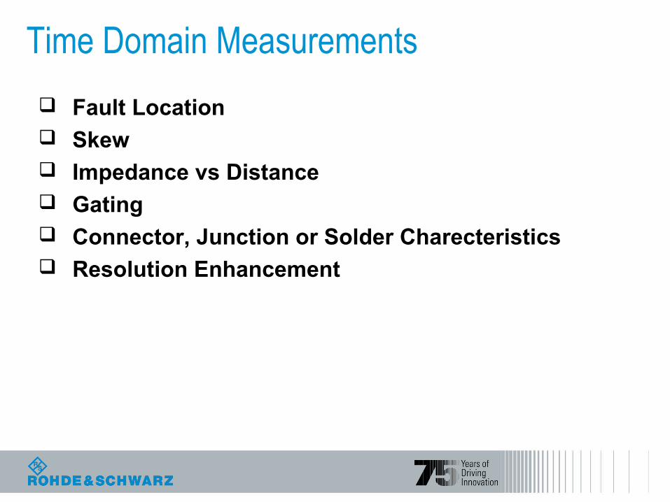
Time Domain Measurements
Fault Location Skew Impedance vs Distance Gating Connector, Junction or Solder Charecteristics Resolution Enhancement
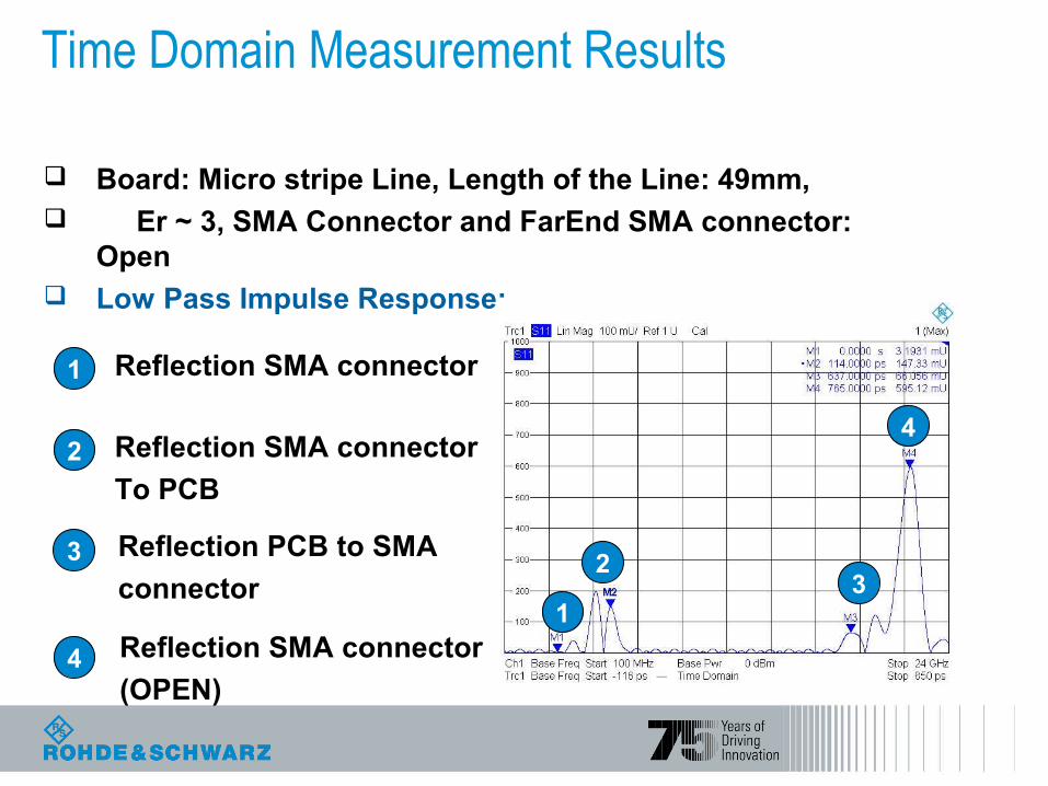
Time Domain Measurement Results
Board: Micro stripe Line, Length of the Line: 49mm, Er ~ 3, SMA Connector and FarEnd SMA connector:
Open Low Pass Impulse Response:
1
1
23
4
Reflection SMA connector
2 Reflection SMA connector
To PCB
3 Reflection PCB to SMA
connector
4 Reflection SMA connector
(OPEN)
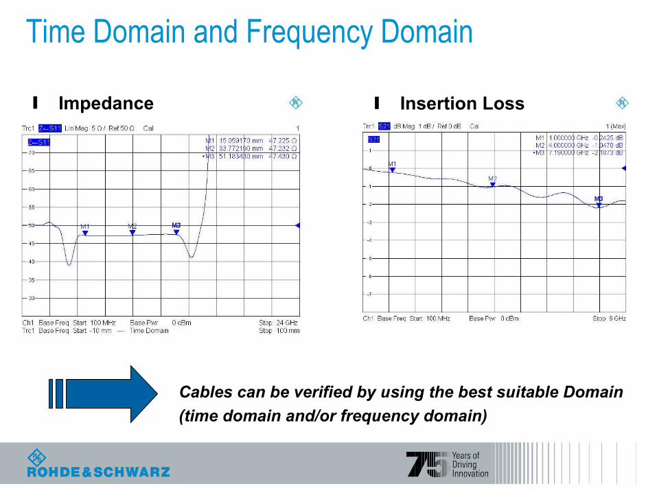
Time Domain and Frequency Domain
l Impedance l Insertion Loss
Cables can be verified by using the best suitable Domain
(time domain and/or frequency domain)
Measurement of a Connector with Time Domain
Gating functionality can be used to suppress unwanted reflections
Gated time domain measurements can be re transformed into frequency domain
Typical application
o Test of the quality of a cable connector
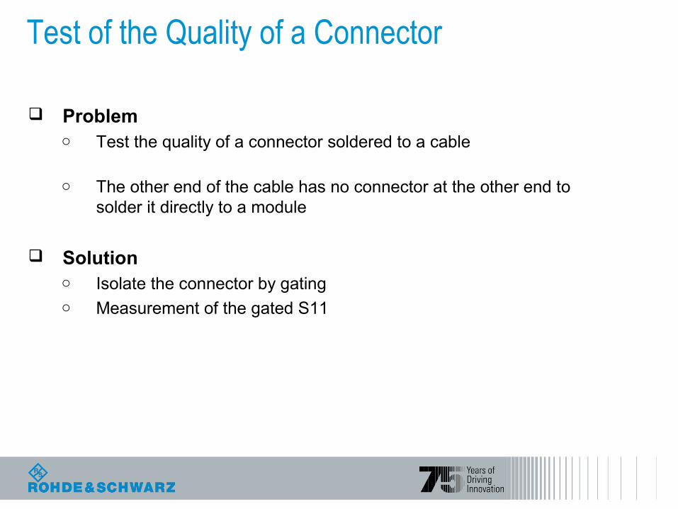
Test of the Quality of a Connector
Problemo Test the quality of a connector soldered to a cable
o The other end of the cable has no connector at the other end to solder it directly to a module
Solutiono Isolate the connector by gatingo Measurement of the gated S11
52
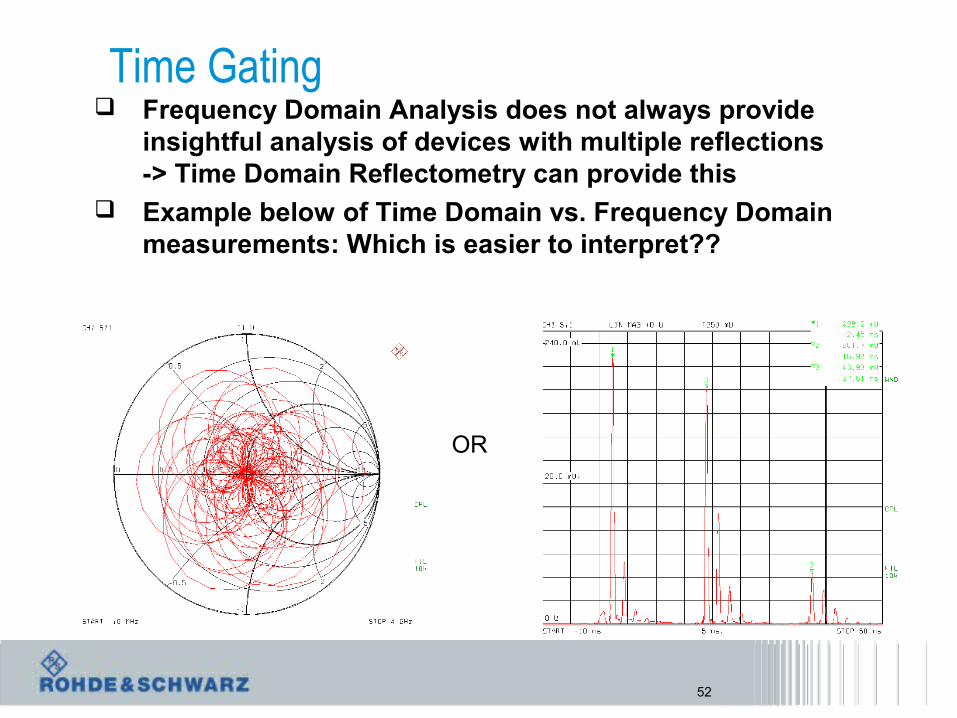
Time Gating Frequency Domain Analysis does not always provide
insightful analysis of devices with multiple reflections -> Time Domain Reflectometry can provide this
Example below of Time Domain vs. Frequency Domain measurements: Which is easier to interpret??
OR

Time Gating (con’t)
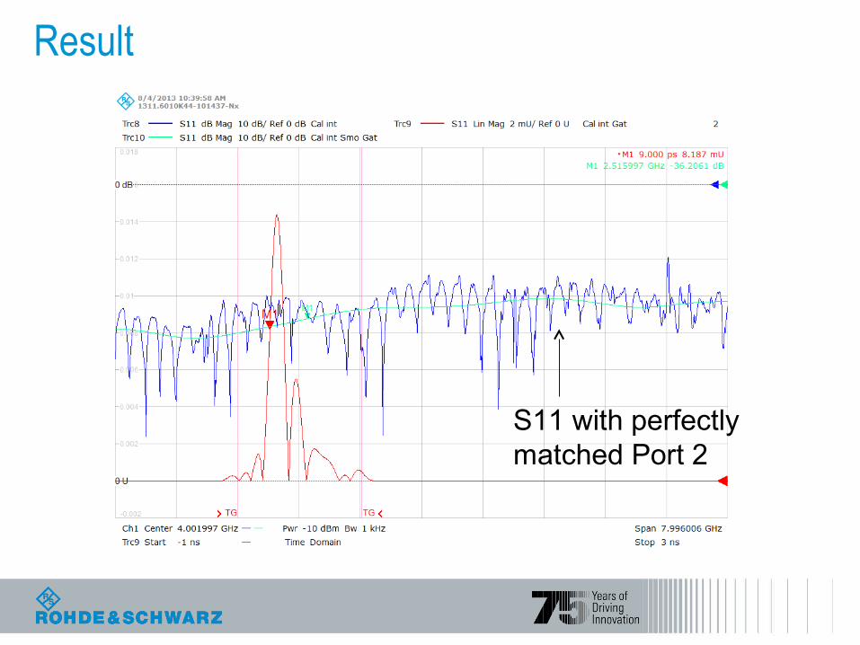
Result
S11 with perfectly matched Port 2
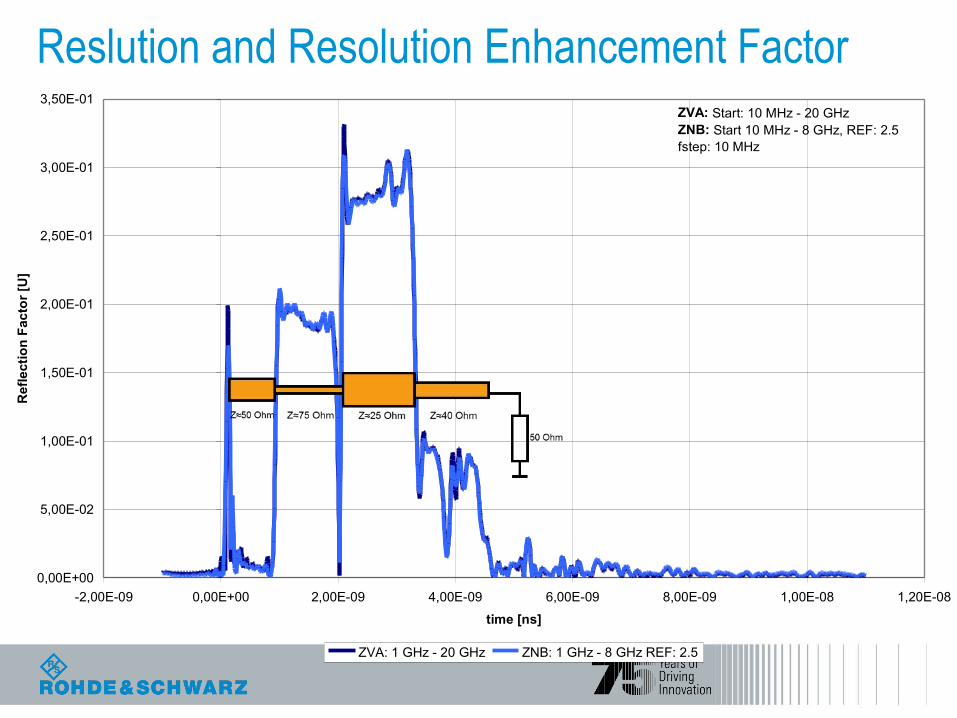
Reslution and Resolution Enhancement Factor
0,00E+00
5,00E-02
1,00E-01
1,50E-01
2,00E-01
2,50E-01
3,00E-01
3,50E-01
-2,00E-09 0,00E+00 2,00E-09 4,00E-09 6,00E-09 8,00E-09 1,00E-08 1,20E-08
time [ns]
Ref
lect
ion
Fac
tor
[U]
ZVA: 1 GHz - 20 GHz ZNB: 1 GHz - 8 GHz REF: 2.5
ZVA: Start: 10 MHz - 20 GHzZNB: Start 10 MHz - 8 GHz, REF: 2.5fstep: 10 MHz
Related Documents


![AppNote - VNA - Calculating VNA Measurement Accuracy [11410-00464]](https://static.cupdf.com/doc/110x72/577ce6641a28abf10392b8aa/appnote-vna-calculating-vna-measurement-accuracy-11410-00464.jpg)