San Jose State University San Jose State University SJSU ScholarWorks SJSU ScholarWorks Master's Theses Master's Theses and Graduate Research 2007 Design and analysis of ultra wide band CMOS LNA Design and analysis of ultra wide band CMOS LNA Janmejay Adhyaru San Jose State University Follow this and additional works at: https://scholarworks.sjsu.edu/etd_theses Recommended Citation Recommended Citation Adhyaru, Janmejay, "Design and analysis of ultra wide band CMOS LNA" (2007). Master's Theses. 3459. DOI: https://doi.org/10.31979/etd.b8b4-7rvn https://scholarworks.sjsu.edu/etd_theses/3459 This Thesis is brought to you for free and open access by the Master's Theses and Graduate Research at SJSU ScholarWorks. It has been accepted for inclusion in Master's Theses by an authorized administrator of SJSU ScholarWorks. For more information, please contact [email protected].

Welcome message from author
This document is posted to help you gain knowledge. Please leave a comment to let me know what you think about it! Share it to your friends and learn new things together.
Transcript

San Jose State University San Jose State University
SJSU ScholarWorks SJSU ScholarWorks
Master's Theses Master's Theses and Graduate Research
2007
Design and analysis of ultra wide band CMOS LNA Design and analysis of ultra wide band CMOS LNA
Janmejay Adhyaru San Jose State University
Follow this and additional works at: https://scholarworks.sjsu.edu/etd_theses
Recommended Citation Recommended Citation Adhyaru, Janmejay, "Design and analysis of ultra wide band CMOS LNA" (2007). Master's Theses. 3459. DOI: https://doi.org/10.31979/etd.b8b4-7rvn https://scholarworks.sjsu.edu/etd_theses/3459
This Thesis is brought to you for free and open access by the Master's Theses and Graduate Research at SJSU ScholarWorks. It has been accepted for inclusion in Master's Theses by an authorized administrator of SJSU ScholarWorks. For more information, please contact [email protected].

DESIGN AND ANALYSIS OF ULTRA WIDE BAND CMOS LNA
A Thesis
Presented to
The Faculty of the Department of Electrical Engineering
San Jose State University
In Partial Fulfillment
of the Requirements for the Degree
Master of Science
by
Janmejay Adhyaru
December 2007

UMI Number: 1452043
INFORMATION TO USERS
The quality of this reproduction is dependent upon the quality of the copy
submitted. Broken or indistinct print, colored or poor quality illustrations and
photographs, print bleed-through, substandard margins, and improper
alignment can adversely affect reproduction.
In the unlikely event that the author did not send a complete manuscript
and there are missing pages, these will be noted. Also, if unauthorized
copyright material had to be removed, a note will indicate the deletion.
®
UMI UMI Microform 1452043
Copyright 2008 by ProQuest LLC.
All rights reserved. This microform edition is protected against
unauthorized copying under Title 17, United States Code.
ProQuest LLC 789 E. Eisenhower Parkway
PO Box 1346 Ann Arbor, Ml 48106-1346

©2007
Janmejay Adhyaru
ALL RIGHTS RESERVED

APPROVED FOR THE DEPARTMENT OF ELECTRICAL ENGINEERING
Advisor Dr. Sotoudeh Hamedi-Hagh Oct 30 ? 07
Co-Advisor Dr. Avtar Sim
Co-Advisor
I A/L^A hA^U^— 10/30/07 / " j Dr. Masoud Mostafavi 1 J*
APPROVED FOR THE UNIVERSITY
••Itfjb ot/ofm
ABSTRACT
DESIGN AND ANALYSIS OF ULTRA WIDE BAND CMOS LNA
by Janmejay Adhyaru
An Ultra WideBand CMOS Low Noise Amplifier (LNA) is presented. Due to
really low power consumption and extremely high data rates the UWB standard is bound
to be popular in the consumer market. The LNA is the outer most part of an UWB
transceiver. The LNA is responsible for providing enough gain to the signal with the
least distortion possible.
CMOS 0.18u TSMC technology has been chosen for the design of the LNA at the
transistor level. As many as five on chip inductors are implemented for the proper gain
shaping over the frequency range of 3.1GHz to 10.6GHz. A noise figure of 4 dB is
achieved to make sure noise contribution of the amplifier is as low as possible.
Agilent's ADS tool has been used to simulate and layout the on chip inductors,
and Cadence's Spectre simulator has been used to simulate the behavior of active and
passive components.

ACKNOWLEDGEMENTS
I would like to thank my MSEE thesis advisor Dr. Sotoudeh Hamedi-Hagh for his
continuous support and encouragement. He worked on strengthening my RF circuit
background and provided a lot of support and guidance to the problems that I faced while
designing this complicated circuit.
I also appreciate the Electrical Engineering Chairperson and my co-advisor Dr.
Avtar Singh and co-advisor Dr. Masoud Mostafavi, for their continuous support. I am
grateful to the Department of Electrical Engineering for providing me with all the
software tools I need to simulate my design.
Lastly I would like to thank my parents, my friends, and all the people who
directly or indirectly helped me in my thesis.
v

TABLE OF CONTENTS
Chapter 1 Introduction to UWB 1 1.1 UWB vs. various wireless standards 1 1.2 UWB applications 3 1.3 UWB operation 4 1.4 UWB transceiver 5 1.5 Choice of technology 8 1.6 Objective 9
Chapter 2 Low Noise Amplifier Characterization 10 2.1 S-parameters 10 2.2 Amplifier's gain and stability 12 2.3 Noise performance 14 2.4 The LNA gain, noise factor, and system sensitivity 17 2.5 Large signal behavior 19
Chapter 3 LNA Design 25 3.1 Popular LNA topologies in CMOS technology 25 3.2 Proposed LNA design 31 3.3 Simulations and results 36 3.4 On chip inductor using ADS 41 3.5 Final layout and extraction 48
Chapter 4 Conclusion 52
References 54
vi
LIST OF FIGURES
Figure 1.1: Datarates for different wireless standards 2 Figure 1.2: ON-OFF pulse keying 5 Figure 1.3: Basic block diagram oftheUWB transceiver 6 Figure 1.4: Block diagram of receiver 7 Figure 2.1: Two-port network 11 Figure 2.2: Single stage RF amplifier block diagram 13 Figure 2.3: Two-port representation of noise using the Z-parameters 15 Figure 2.4: Two-port representation of noise using the Y-parameters 16 Figure 2.5: Noise factor calculation 17 Figure 2.6: Interference from adjacent channel 19 Figure 2.7: Two-tone test to measure linearity of the LNA 20 Figure 2.8:1 -dB compression point 21 Figure 2.9: SFDR definition 22 Figure 2.10: Compression-Free Dynamic Range 23 Figure 3.1: Resistive terminated LNA 26 Figure 3.2: Common gate LNA 26 Figure 3.3: Shunt series feedback LNA 27 Figure 3.4: Current reuse LNA 28 Figure 3.5: Cgd neutralization LNA 29 Figure 3.6: Inductive source degeneration LNA 30 Figure 3.7: Proposed inductive source degeneration schematic 32 Figure 3.8: Gain vs. frequency simulation 36 Figure 3.9: LNA schematic with ports 37 Figure 3.10: Noise figure simulation 37 Figure 3.11: GA,GT and GP simulation 38 Figure 3.12: 1-dB compression point 39 Figure 3.13: IIP3 simulations 40 Figure 3.14: The spiral inductor-II model 42 Figure 3.15: Pi-model generated in ADS 43 Figure 3.16: Inductor of 1.6 nH 44 Figure 3.17: S-parameter results for the spiral inductor 45 Figure 3.18: Generation of the Z-parameters in ADS 46 Figure 3.19: Simulated values of Q, L and r from Z-parameter 47 Figure 3.20: Layout without capacitors and inductors 49 Figure 3.21: Final layout 50
vii

LIST OF TABLES
Table 1.1: Typical UWB receiver front-end specifications for LNA 7 Table 1.2: The TSMC technology process parameters from MOSIS Service 8 Table 2.1: Typical parameters of a UWB receiver 24 Table 3.1: Comparison between various topologies 31 Table 3.2: Component sizes for the LNA design 35 Table 3.3: Comparison between targeted and achieved results 40 Table 3.4: Substrate information of the inductor 43 Table 3.5: Inductor dimensions 44 Table 3.6: Comparison of results before and after inserting pi-models for inductors 48 Table 3.7: Comparison between schematic and extracted simulations 50 Table 3.8: Summary of comparison of this work with past works in LNA 51
viii

Chapter 1 Introduction to UWB
1.1 UWB vs. various wireless standards
Ultra WideBand (UWB) technology has been designed to bring convenience and
mobility of high speed wireless communication to homes and offices. It is specifically
designed for short range Wireless Personal Area Networks (WPANs). UWB will play an
instrumental role in freeing people from wires and enabling video transmission or other
high bandwidth data transmission that is rarely possible with a conventional wireless
connection.
The short range UWB technology will also complement other wireless standards
such as Wi-Fi and Wi-Max. It can transmit data within the radius of 10 meters from the
host device. UWB technology is designed to provide a short range, very low power
connection with much more bandwidth than cable. Since UWB communicates with short
range pulses, it can be used for tracking various objects.
It has been shown that a UWB device can successfully transmit data at a rate of
110 Mbps at a distance of 10 meters [1]. This bandwidth is 100 times faster than
Bluetooth and twice as fast as Wi-Fi. This bandwidth is large enough to accommodate
three concurrent video streams over a single connection. Designers are promising UWB
products that have speeds of up to 1 Gbps [2]. A chart comparing the data-rates of
different wireless technologies is shown in Figure 1.1.
1

PAN
LAN
Wireless MAN
Cellular (
1 • >
Bluetooth C I
Ultrawideband
f Wi-Fi 802.11 J
f 802.16
2G/2.5G/3G
1 )
)
)
0.01 0.1 1.0 10 100 1000
Figure 1.1: Data rates for different wireless standards
The implementation of UWB for data transmission through radio channel has the
following advantages compared to narrow-band signals:
• UWB standard consumes very low average radiated power, which is usually
expressed in units of miliwatts, though sometimes it depends on distance between
the UWB transmitter and receiver.
• Since the spectral power per frequency band is very low, UWB communication is
very secure. It is also electromagnetically compatible with narrow-band systems
operating within the same frequency band.
• The higher bandwidth of UWB standard provides data rates up to 1 Gbps.
• UWB communication is robust to multi-path signal propagation due to the time
selection of direct and re-scattered signals, and the correlation reception.
It is clear that UWB is a growing technology aiming to replace all other
narrow-band technologies for short range communication.
2

1.2 UWB applications
The benefits of low power and high data rate of the UWB standard promises a
great range of applications in the military, civilian, and commercial sectors. A brief
summary of UWB applications is presented here.
UWB applications are categorized in three major areas: radar, imaging, and
communication [2]. Radar is one of the most powerful applications of this technology.
Narrow UWB pulses have fine positioning characteristics, and this particular trait enables
them to offer higher resolution radar for military and civilian applications. Also,
penetration of objects is possible because of the very wide frequency spectrum. In the
commercial world, these types of radar systems can be used on construction sites to
locate pipes, studs, and electrical wirings. The same technology can be used in medical
applications such as a remote heart monitoring system. In the automotive industry it
could be used to develop or enhance collision avoidance systems.
The low transmission power of UWB pulses makes UWB system ideally suited
for military communication. Low power UWB pulses are extremely difficult to detect or
intercept, which makes any UWB system very secure. UWB devices are much simpler as
far as circuitry is considered, and can be manufactured in smaller size and at a lower cost
than narrow-band systems. Small and inexpensive UWB transceivers are very useful in
wireless sensor network applications for both military and civilian use. Such sensor
networks can be used to detect physical objects, and transfer the detected information to a
chosen destination. For military application a UWB system could provide detection of a
biological agent or the location of the enemy on the battlefield. In the commercial sector
3

UWB applications may include habitat monitoring, environment observation, health
monitoring, and home automation.
UWB can also connect Personal Computer (PC) and other entertainment
components to a media PC or a mobile notebook PC for editing, compiling, and sending
pictures or other multimedia files. UWB provides a fast and high quality connection.
With UWB-enabled Wireless Private Area Networks (WPANs), once the devices are
within the proximity, they can automatically recognize each other.
1.3 UWB Operation
A UWB signal can be defined as a signal in which the range of the frequency
utilization factor changes between 0.25 and 1 and is defined by:
tup " MOW
Tl= fup+ flow (1.1)
where fup is the highest frequency of the frequency band and fiow is the lowest frequency
of the frequency band.
UWB system makes efficient use of the basic behavior of UWB signals. The use
of UWB short duration signals helps to maintain the high quality of the data transmitted.
A reduction in the radiated pulse duration causes an efficient resistance to multi-path
signal propagation, which is often generated by the signal re-scattering from objects
located near the communication system antenna and from the line of sight between the
signal source and the receiver. If the duration of the signal is 1.0 ns, and the objects
4

which cause signal re-scattering are located at a distance of more than 30 cm from the
line of sight, the result will be undistorted signal detection [2].
Figure 1.2 explains ON-OFF pulse keying for a pulse duration of 1.0 ns. The
pulse repetition frequency is 2.0 MHz. This type of modulation is suitable for UWB
systems.
Unit bit
t
Figure 1.2: ON-OFF pulse keying
There are several methods to implement a UWB system. The next section
discusses basic UWB architecture.
1.4 UWB transceiver
A basic block diagram of the UWB transceiver, including a transmitter and a
receiver, is shown in Figure 1.3. The baseband Digital Signal Processing (DSP) unit
controls the messaging and signaling of information. The DSP unit also synchronizes the
system clock. The main function of the receiver is to amplify the signal without
amplifying the noise. The principal role of the transmitter is to boost up the signal using
some line drivers in order to send high energy signals.
5

I - *
Receiver Unit
Transmission Unit
4
Digital Signal
Processing Unit
(DSP)
Figure 1.3: Basic block diagram of the UWB transceiver
The block diagram of a UWB receiver is shown in Figure 1.4. The receiver
features a Low Noise Amplifier (LNA) followed by a mixer (demodulator). The mixer
removes the carrier from the received radio frequency signal. Usually there is an
automatic gain control block between the mixer and the Analog to Digital Converter
(ADC). The purpose of this block is to balance the amplification or attenuation of the
received signal in a way that it utilizes the maximum range of the ADC. The analog to
digital converter then converts the analog signals to digital data which is fed to the DSP
to process the transmitted data. The signal is then fed to the DSP block for baseband
processing. In this context it is clear that an ultra wideband LNA should pass all the
frequencies between 3.1 to 10.6 GHz. Such an amplifier must feature wideband input
matching to a 50 Q antenna for noise optimization and filtering of the out-of-band
interferers. Moreover, it must show flat gain with good linearity and minimum possible
noise figure over the entire bandwidth.
6

Antenna AGC
Mixer
ADC
ADC
Digital Baseband
Mixer
AGC
Figure 1.4: Block diagram of receiver
The LNA is an instrumental component of a UWB receiver. The LNA's noise
figure has a major impact in deciding the system's overall noise figure, therefore this
thesis deals with various aspects of the LNA design for a UWB device. The general
specifications of a typical UWB LNA are listed in Table 1.1.
Table 1.1: Typical UWB receiver front-end specifications for LNA
Operating frequency
Gain
Noise figure
1-dB compression point
IIP3
< 10 GHz
> 8 d B
< 3 d B
-15 to 5 dB
-10to5dB

1.5 Choice of technology
CMOS and Silicon Germanium are the main processes to implement RF circuits.
Low power consumption and easy availability were the main reasons to choose the
CMOS process for this thesis. TSMC 0.18|J CMOS technology was selected to design
the LNA. This technology is available to the university lab from Metal Oxide
Semiconductor Implementation Services (MOSIS). Table 1.2 shows some of the process
parameters.
Table 1.2: The TSMC technology process parameters from MOSIS Service
No. of metal layers
Supply voltage
ft of transistor
Metal 6 Thickness
Substrate to metal 6 distance
6
1.8 V
40 GHz
0.99 um
5 um
The ft of the transistor is the unity current gain frequency. It is also known as
cutoff frequency which is defined as the signal frequency at unity gain when the
transistor is used as an amplifier. In other words, all the parasitic capacitors in the
transistor become short-circuited at this frequency. TSMC 0.18|J CMOS technology
consists of 6 metal layers and 1 poly-silicon layer which is designed for high speed low
voltage applications. Metal 6 is the outer most of all the layers, and it is used for laying
out the inductors.
8

1.6 Objective
This thesis mainly focuses on all five band groups of the UWB standard, and
discusses different aspects of the LNA design. The basic objective of the LNA design is
to get good gain with minimum noise generation for the entire UWB operating frequency.
The gain aimed for this UWB LNA is greater than 8 dB, and the noise figure targeted is
less than 3 dB for the entire band of 3 to 10 GHz. Along with good gain and noise figure,
good linearity is also required for the LNA to operate properly. Thel-dB compression
point and IIP3 point are the characteristics measuring the linearity of the RF components.
The objective is to get -10 dB of 1-dB compression point and IIP3 of-12dB. The
targeted power dissipation is less than 20 mW.
Chapter 2 mainly focuses on the different characteristics of the LNA and how
these traits affect the overall design. Chapter 3 discusses some popular topologies and
the proposed LNA architecture along with providing simulation results. Chapter 3 also
discusses implementation of the on-chip inductors using Advance Design System (ADS).
Finally, Chapter 4 concludes the thesis.
9

Chapter 2 Low Noise Amplifier Characterization
The Low Noise Amplifier (LNA) is the first gain stage of a receiver. It must meet
several specifications at the same time, which makes its design challenging. The signals
coming from the receiver antenna are very small, usually from -100 dBm (3.2 V) to -70
dBm (0.1 mV), therefore signal amplification is needed before it is fed into the mixer.
This process sets the requirement of a certain gain to the LNA. The received signal
should have a certain Signal to Noise Ratio (SNR) in order to allow proper detection.
Therefore, noise added by the circuit should be reduced as much as possible. A large
signal or blocker can occur at the input of LNA. The circuits should be sufficiently linear
in order to have a reasonable signal reception. For portable and mobile applications,
reasonable power consumption is another constraint.
The gain, stability and noise figure of the LNA are usually measured using the
scattering parameters (S-parameters), which will be studied in the next section.
2.1 S-parameters
The scattering parameters or S-parameters are widely used in microwave and RF
circuit analysis. S-parameters are used to model and characterize an n-port linear
network [3]. The linear equations describing the behavior of the two-port network using
S-parameters are:
b1 = S11*a1 + S12*a2 (2.1)
b2 = S2i*ai + S22*a2 (2.2)
where bi, b2, ai and a2 are traveling waves representing incident voltages at the ports.
10

The S-parameters Sn, S22, S21 and S12 are defined by:
Sn = (bi / ai) where a2 = 0
S22 = (b2 / a2) where ai = 0
S21= (b2 / ai) where a2 = 0
S12 = (bi / a2) where ai = 0
(2.3)
(2.4)
(2.5)
(2.6)
For most measurements and calculations, it is convenient to assume that the port
reference impedances Zs and ZL are positive and real. Ii and I2 are currents referring to
the input and output ports, respectively. One such model is shown in Figure 2.1. Each
port can have distinct reference impedance, but the same reference impedance Zo will be
used for all the ports here.
" ' 12 r AAAr Zs
ACfU Linear
Two-port Network
Figure 2.1: Two-port network
The independent variables ai and a2 can also be related to port voltages (Vi, V2)
and currents (Ii, I2) as follows:
a i = (Vi+I1Z0)/(2VZo) (2.7)
a2= (V2 + I2Z0) / (2 VZ0) (2.8)
Similarly, the dependent variables bi and hi can also be related to port voltages
and currents as follows:
b!= (V1-IiZ0)/(2VZo) (2.9)
bi= (V2-I2Zo)/(2VZo) (2.10)
11

From the above explanation of ai, a2, bi, and b2, the four S-parameters are simply
related to power gain and mismatch loss:
IS1112 = (Power reflected from the input) / (Power incident on the input) (2.11)
IS22I = (Power reflected from the input) / (Power incident on the output) (2.12)
IS2112 = (Power delivered to the load) / (Power available at the source) (2.13)
IS12I2 = Reverse transducer power gain with Zo load and source (2.14)
2.2 Amplifier's gain and stability
There are two criteria that affect the gain performance of any RF amplifier: the
RF transistor itself and the input output matching network. A simplified block diagram is
shown in Figure 2.2. The amplifier is characterized by its S-parameters and terminated
by the source and load impedance Zs and ZL, respectively. Sn and S22 are the input and
output reflection coefficients. The load of the next stage follows the output matching
network. The input and output reflection coefficients r,n and rout for a two-port network
are [4]:
r i n = (bi / a2) = S u + (S12 S21rL/ (1 - S22rL)) (2.15)
rout= (b2/ a2) = S22+ (S12 s2ir s/ (l - s„r ,)) (2.16)
where
r L =(Z s -Z 0 ) / (Z s +Z 0 ) (2.17)
r s =(Z L -Z 0 ) / (Z L +Z 0 ) (2.18)
12

where lY is source reflection coefficient, r s is load reflection coefficient, and ZQ is
reference impedance.
-a l*
«bl-
- b >
*a2-
A/W-i Zs ACfU
Input matching network
RF amplifier
Output Matching network
ZL
Figure 2.2: Single stage RF amplifier block diagram
If the input and output are simultaneously complex conjugate matched, i.e. Tin
=r*s and r0ut = T*L, the amplifier has maximum power transfer. Achieving the
simultaneous complex conjugate matching condition is not easy. A special case is for a
unilateral device where Sn is practically zero, then Tin = Sn and r o u t = S22- If the input
and output are decoupled from each other, matching can be done at the input and output
separately.
Several gain definitions exist for an amplifier. Power gain (G) characterizes the
actual power amplification of an amplifier, and it is defined by:
Available power at output
(2.19) Power gain =
Power at the input
Available power gain (GA) shows the maximum possible power amplification of
the amplifier. For IC implementations, the LNA input is interfaced off-chip and is
usually matched to specific impedance (50 Q or 75 Q). An LNA's output is not
13

necessarily matched when it is directly driving on-chip blocks such as mixers [5]. This
situation is usually characterized by LNA's voltage gain or transducer power gain.
The voltage gain (Ay) is defined as the voltage at the output port divided by the
voltage at the input port of the amplifier and is given by:
A V = (v2 / v,) = [ s2i (l + rL)] / [ (l - s22rL) (1 + r in) ] (2.20)
The transducer gain (GT) is defined as power delivered to the load divided by the
power available at the source [6]:
G T = (PL /PAVS) (2.21)
where PL equals the power incident on load minus the power reflected from load. PAVS is
the power available at the source.
PL = | b 2 | 2 ( l - | r f ) (2.22)
2.3 Noise performance
The noise performance of an RF amplifier is represented by its noise factor or
noise figure. The noise factor accounts for the degradation of the signal's SNR due to the
amplifier. It is defined as the SNR at the input of the network divided by the SNR at the
output of the network [7]:
F = (SNRin/SNRoUt) (2.23)
where SNRjn and SNRout are the SNRs at the input and output of the amplifier,
respectively. The noise factor represents the signal's quality in terms of noise before and
after the network. The noise figure is the same as the noise factor expressed in dB.
NF(dB) = 101ogF (2.24)
14

It would be complex if one tried to use a transistor's equivalent noise circuit to
analyze the whole amplifier or network. A two-port network noise model can simplify
the calculation of its noise factor of a network. An effective way to analyze noise in a
given circuit is to assume that the circuit is noiseless, and to model its internal noise by
external noise sources at the input and output ports of the circuit. These noise sources
must have the same noise power appearing at the circuit's terminals as the original noisy
circuit. The noiseless network can be represented by its Z- and Y-parameters. In the
following discussions, it is assumed that port 1 is the input port and port 2 is the output
port.
Using the Z-parameters in Figure 2.3, the voltage-current relationship among
ports can be written as:
V ^ Z n I i + Z ^ + Vm (2.25)
V2 = Z21Ii+Z22l2 + Vn2 (2.26)
The equivalent noise source Vni and V„2 can be measured from the open-circuited
measurements as:
Vm = Vi where ii=i2=0 (2.27)
V„2 = V2 where ii=i2=0 (2.28)
t - Y T > V,
w
Noiseless Netwak
fT^« v2
w
Figure 2.3: Two-port representation of noise using the Z-parameters
15

Using the Y-parameters in Figure 2.4, the voltage-current relationships among
ports can be written as:
I ^ Y n V i + YuVz + Im (2.29)
l2 = Y21V1 + Y22V2 + In2 (2.30)
The equivalent noise source Ini and In2 can be obtained from the short-circuited
(s.c.) measurements as:
Im = Ii where Vi=V2=0 (2.31)
In2 = h where Vi=V2=0 (2.32)
II -— •
w
>
Noiseless Network 4 ^ In2
12
•
V
9
Figure 2.4: Two-port representation of noise using the Y-parameters
Referring the noise sources to the input port is convenient for the noise analysis.
Therefore, the noise factor of a two-port network can be calculated using the noise
representation in Figure 2.5. Consider a general network with a noise current source
connected at its input port as shown in Figure 2.5. It is assumed that the noise of the
source and the noise of the network (In and Vn) are uncorrected, but the possibility exists
for cases where Vn and In may be correlated.
The total output noise power is proportional to the mean square value of the short-
circuited current (Isc) at the input port, whereas the input noise power is proportional to
the mean square value of the source current (Is). The noise factor is then calculated by:
16

H vnl
ft) Noiseless Network
V„2 12
v2
w
Figure 2.5: Noise factor calculation
F = [(mean square of Is.c.) / (mean square of Is)] (2.33)
where Isc. = [mean square of Is + mean square of (I„ + VnYs)] and Ys is the source
admittance.
So, it is clear from the above discussion that it is easier to analyze the noise when
the circuit under analysis is assumed to be noiseless and noise is seen as an external
effect. The next section describes the system sensitivity and its dependence on the gain
and noise factor.
2.4 The LNA gain, noise factor, and system sensitivity
The importance of the gain and noise factor specifications on an LNA can be
discussed further from the receiver's system sensitivity aspect. The smallest input signal
power that can be reliably detected by the system is called the system sensitivity (Ps):
Ps = 174dBm + 10 log BW + SNR + 10 log Ftot (2.34)
The first two terms in equation 2.34 are usually referred to as the noise floor. BW
is the system bandwidth and is determined by a specific application. For UWB
application BW should be approximately 7.5 GHz. The SNR is determined by the Bit
Error Rate (BER) requirement of the system. For example, for a UWB receiver,
simulation shows that an 8 dB SNR is needed for a BER lower than 10 , and for an
17

802.lib receiver, an 11.4 dB SNR is required to achieve better than 10" BER. Ftot is the
system's total noise factor, and it is directly affected by the LNA's gain and noise factor.
Ftot can be calculated by:
Ftot= FLNA + [(FafterLNA- 1 ) / G L N A ) ] (2.35)
where FLNA is noise figure of the LNA, GLNA is the current gain of the LNA, and FafterLNA
is noise figure of the system excluding the LNA.
Equation 2.35 shows that the LNA's noise factor FLNA appears directly in the
system's noise factor. For high sensitivity a low system noise factor is required, therefore
FLNA should be made as small as possible. The second term of equation 2.35 shows that
noise coming from the stages following the LNA will be suppressed by the LNA's gain;
hence a high gain LNA is desirable for high sensitivity. For example, in a UWB receiver,
if the LNA's noise figure is 3 dB, its available power gain GLNA is 8 dB and the overall
noise figure of the circuits following the LNA is 18 dB, then the system's total noise
figure can be found using equation 2.35 to be 7.4 dB. If the LNA's gain is increased to
15 dB, the total noise figure will be reduced to 4.1 dB, and the system sensitivity will be
improved by 3.3 dB. If the 7.4 dB noise figure is a fixed system specification, the noise
figure requirement on the circuits after the LNA can be relaxed to 24 dB. On the other
hand, a high gain of the first stage, which is the LNA in this case, will put a more
stringent linearity requirement on the following stages. Therefore a trade off must be
made amongst gain, noise, and linearity.
18

2.5 Large signal behavior
The RF amplifier is a non-linear system in nature. If the input signal is small
enough, the circuit can be modeled using a linear model around its operating point. But if
the signal level is relatively high, due to the non-linearity, the amplifier's dynamic
operation point will be changed and will become a function of the signal level. The
LNA's proper operation must be checked by using a large signal input. On the other
hand, although the signal itself is small, large interferers may come together with the
signal. This situation is shown in Figure 2.6, where fa and fi, are upper and lower bound
frequencies of the desired spectrum and fi and f2 are external interferers. The interferers
can come from the adjacent channel or can be generated by an intentional jamming
system.
IM3 F = 2f,-f2
fa<2fi-f 2<f b
fa ft fi f2
Figure 2.6: Interference from adjacent channel
Interference specifications are usually provided by the system standards. The
non-linearity of performance is characterized by the two-tone test (fi, fj) as depicted in
Figure 2.7. Usually, the distortion terms (2fi - fi) and (2f2 - fl) fall in-band, and are
characterized by 3rd order non-linearity. For example in a UWB receiver, the desired
19

signal channel in Figure 2.7 has a bandwidth of 7.5 GHz and is centered at 6 GHz. Two
large blockers are located at 12 GHz and 18 GHz, which are separated by 6 GHz. Thus
the lower side IM3 component will be at (2fi - f2) = 6 GHz, which is directly upon the
center of the channel. A large in-band blocker tends to desensitize the circuit. The 1-dB
compression point measures the effects of intermodulation.
fl f2
ft fi
2f,-f2
o-\ LNA
Inter-modulation product
2f2-f, A
Figure 2.7: Two-tone test to measure linearity of the LNA
2.5.1 1-dB compression point
The 1-dB compression point (PldB) is the point (input or output) where the
fundamental gain is reduced by 1 dB from the ideal small signal gain at a certain
frequency. Assuming that the non-linear system can be approximated by the Taylor
senes:
Y(t) = ctix(t) + cc2x2(t) + a3x
3(t) +
The 1-dB compression point can be calculated as:
(2.36)
PidB= V [0.145 (cti/cfc,)] (2.37)
where oti and 0:3 are the lst-order and 3r -order coefficients of the Taylor series expansion
of the system's input/output characteristics as in equation 2.36. The 1-dB compression
point is illustrated in Figure 2.8.
20

1 dB
Pin (dBm) •
Figure 2.8: 1-dB compression point
2,5.2 Intercept point
The two-tone test can also show the impact of a potential interferer on the desired
signal. Due to the non-linearity of the circuit, the 2nd and 3rd order inter-modulation
products will appear at the output and may lie within the pass band, which can degrade
the quality of the output signal.
Typically, the desired output (fundamental), the 2nd order inter-modulation output
(IM2), and the 3rd order inter-modulation output (IM3), are plotted as a function of the
input signal level. The 2nd order intercept point (IP2) is the extrapolated intersection of
the fundamental curve and the IM2 curve. The 3rd order intercept point (IP3) is the
extrapolated intersection of the fundamental and IM3 curves. For the system described
by equation 2.36, the input-referred IP3 (IIP3) is given by:
IIP3 = Vl .33 (a i / a 3 ) (2.38)
Pout (dBm)
21

2.5.3 Dynamic range
In simple words, dynamic range can be defined as the ratio of maximum to
minimum input levels at which the circuit operates with reasonable distortion and output
signal quality. Two different definitions are usually used: Spurious-Free Dynamic Range
(SFDR) and Compression-Free Dnamic Range (CFDR).
Figure 2.9 shows the definition of SFDR. The upper bound of SFDR is based on
inter-modulation behavior, and is defined as the maximum input level in a two-tone test
for which the 3r order inter-modulation (IM3) products do not exceed the noise floor. It
can be shown that the input level for which the IM3 products become equal is:
Pin,max=(2*IIP3*N f l o o r)/3 (2.39)
where Nfioor =174 dBm + NF + 10 logBW, is the noise floor. All the quantities are
expressed in dBm. The lower bound of SFDR is limited by the system sensitivity. If for
a certain required signal quality the minimum SNR is SNRmi„, then the minimum
detectable signal level in dBm at the input is:
Minimum detectable
level i
lse tloor
Testing tones i
k
L i [ T 1 SFDR 1 I
i
\
SNRmin
t 2f,-f2 fi f2 2f2-f, 2 - 1 1
Figure 2.9: SFDR definition
22

Pin;min = S N R m i n + N f l o 0r ( 2 . 4 0 )
This process is also shown in Figure 2.9. The SFDR is then calculated by the
difference between Pin;max and Pm;min:
SFDR = 0.66 (IIP3 - N F - lOlogB + 174 dBm) - SNRmin (2.41)
Compression-Free Dynamic Range (CFDR) is the difference, in dB, between the
input-referred 1-dB compression point and the noise floor as shown in Figure 2.10:
CFDR = PldB-Nfl00r (2.42)
Pout f (dBm)
Nfloor PldB
Pin (dBm) •
Fig. 2.10: Compression-Free Dynamic Range
Here is a numerical example. Suppose an UWB receiver has the system
specifications as shown in Table 2.1.
23

Table 2.1: Typical parameters of a UWB receiver
Parameter
SNRmin
BW
IIP3
NF
Value
3dB
7.5 GHz
-13 dBm
4dB
The noise floor Nfl00r calculated from the above data is -40 dBm. From equation
2.39 and 2.40, Pin;max and Pin;min are -22 dBm and -37 dBm, respectively. Thus SFDR is
42 dB. The 1-dB compression point can be estimated from the IIP3, which is usually 10
dB larger than PldB, therefore CFDR is about 46 dB.
In this chapter of the thesis different parameters of the LNA were discussed.
These parameters can affect the functionality of the LNA. Careful consideration of all
these parameters can result in a fully working LNA. The next chapter discusses various
popular LNA topologies along with a proposed LNA with results.
24

Chapter 3 LNA Design
3.1 Popular LNA topologies in CMOS technology
The LNA usually only involves one or two transistors to achieve low noise
operation. The performance of the LNA circuits is very dependent on process
technology. CMOS technologies are the best choice to design an LNA because they offer
high speed operation, simplicity in fabrication, and low power consumption. The
following discussion presents several popular LNA structures possible in a CMOS
integrated circuit. The LNA input is directly connected to a filter for impedance and
noise matching. Therefore, different LNA structures have different methods to achieve
impedance matching.
The structure shown in Figure 3.1 achieves input impedance matching by directly
placing a 50 Q resistor (Rs) in parallel with the gate of transistor Ml. This is the most
straightforward method but the noise figure will be exceptionally high. The lower bound
of the LNA noise factor is given by:
F > 2 + (4y/agmRs). (3.1)
where a = gm/gdo, gdo is the drain source conductance, and y is a constant with a value of
0.66. Since the term (y / ocgmRs) is larger than 1, the noise figure is readily larger than 6
dB. The primary contribution of noise comes from the termination resistor Rs and the
drain of the transistor. Due to the noise performance limitations this LNA structure is
rarely used [3].
25
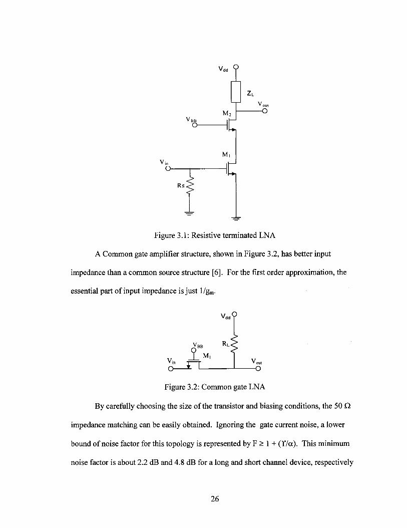
VBB O
O
Rs.
Vdd 9
M,
M,
Figure 3.1: Resistive terminated LNA
A Common gate amplifier structure, shown in Figure 3.2, has better input
impedance than a common source structure [6]. For the first order approximation, the
essential part of input impedance is just l/gm.
VddP
Vin
o-
v B B
_ L Mi
Ri.
Vou, —O
Figure 3.2: Common gate LNA
By carefully choosing the size of the transistor and biasing conditions, the 50 Q
impedance matching can be easily obtained. Ignoring the gate current noise, a lower
bound of noise factor for this topology is represented by F > 1 + (Y/a). This minimum
noise factor is about 2.2 dB and 4.8 dB for a long and short channel device, respectively
26

[3]. The gate current noise will make the noise factor larger, but the drain noise will still
be the dominant factor.
The shunt series feedback LNA, shown in Figure 3.3, uses negative shunt
feedback to modify the input impedance of a common source stage. Its input impedance
can be approximately calculated by:
Zin = R F / ( l + A ) (3.2)
where A is the voltage gain which is approximately in the order of Ri/Ri assuming the gm
of Mi is very large.
vdd o
RF
HVW RL
o-
M,
<£,
R L
Figure 3.3: Shunt series feedback LNA
The noise figure of this structure is better than that of the resistively terminated
LNA structure but it is still too high to use in applications such as a UWB receiver. The
gate noise is the largest noise contributor in the shunt series feedback LNA structure.
This is because the gate noise current experiences high impedance due to the resonance
of the input matching network. Therefore, in order to reduce the noise figure, the quality
27

factor of the input matching network should be reduced leading to an impact on the signal
quality and filtering.
The basic issue with using a CMOS transistor for the LNA is its inherently low
transconductance and hence low gain. However, if the current reuse technique is
employed, transconductance could be increased as much as two-fold. Figure 3.4 shows a
simplified schematic of the current reuse LNA. The key point is that given the same bias
current the effective transconductance is gmi + gni2, while it is simply gmi in the case of
the topologies mentioned previously. A major drawback of this design is its high input
and output impedances, thus requiring external impedance matching networks. This
prevents the use of this LNA in fully integrated applications. Due to the high gain
property, the strong Miller effect reduces the reverse isolation of this LNA. In the actual
design, two identical stages are cascaded to improve the reverse isolation.
0
M2
M,
M3
>
-O
-O
Fugure 3.4: Current reuse LNA
28
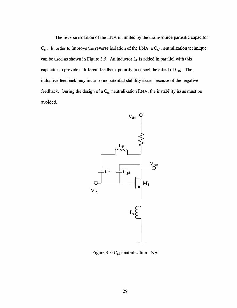
The reverse isolation of the LNA is limited by the drain-source parasitic capacitor
Cgd. In order to improve the reverse isolation of the LNA, a Cga neutralization technique
can be used as shown in Figure 3.5. An inductor LF is added in parallel with this
capacitor to provide a different feedback polarity to cancel the effect of Cgd. The
inductive feedback may incur some potential stability issues because of the negative
feedback. During the design of a Cgd neutralization LNA, the instability issue must be
avoided.
Vdd o
o-
LF
4=CF =^C
V,-,
•-gd
v o u t V
M i
Figure 3.5: Cgd neutralization LNA
29

Figure 3.6 shows the structure of the inductive source degeneration LNA which is
used for the design of LNA for this thesis. Transistor Mi is in the common source
configuration and M2 is in the common gate configuration, which has a benefit of higher
input impedance. Degeneration inductor Ls provides negative feedback to the amplifier
and stabilizes the gain.
Vdd O
M,
B6-
ZL
V^u,
M,
'•^J—L
4=c gs
3.6: Inductive source degeneration LNA
Table 3.1 compares all the topologies discussed before. As shown in Table 3.1 it
can be proven that inductive source degeneration LNA has a good narrowband match and
a very small noise figure. Good input output match and noise figure are essential
requirements for any UWB LNA design. Since UWB is such a low power technology,
one cannot afford to add too much noise into the system. Research has shown that the
30

source degeneration is the best suitable topology for the UWB related LNA [7]. The next
section discusses proposed design and simulations for the source degeneration LNA.
Table 3.1: Comparison between various topologies
Topology
Resistive termination
Common gate
Series shunt feedback
Inductive degeneration
Current resue
Inductor neutralization
Plus Point
Good input match
Excellent input match
Broadband i/o match
Good narrowband match,
Small NF
High gain low power
Good reverse isolation (S22)
Minus Point
Large NF
Huge NF and power
Stability issues
Large area
External matching
network required
Increased area, stability
concerns
3.2 Proposed LNA design
The proposed schematic is shown in Figure 3.7. A Chebyshev filter is used to
achieve resonance in the reactive part of the input impedance over the whole frequency
range of 3.1 to 10.6 GHz. Typically the Chebyshev filter consists of two capacitors and
two inductors. The Chebyshev filter works as a passband filter if the sizes of Li, Ci, L2
and C2 are selected correctly.
31

Vdd 0 Vdd O
:RL
M3
Filter
Vbi!
r\^r>r>.
M2
M i
r
M4
>ias 11 1
Figure 3.7: Proposed inductive source degeneration schematic
The proposed solution expands the basic inductively degenerated common source
amplifier by inserting an input multi section reactive network, so that the overall
reactance can be resonated over a wider bandwidth. This input matching network is
shown in the Figure 3.7 by a dotted square. An inductor (Lg) is placed in series with a
capacitor (Cp) to add flexibility to the design. Different values of Lg and Cp would give
different matching conditions. The cascade connection of Mi and M2 improves the input
output reverse isolation and the frequency response of the amplifiers. The source
follower stage (M3 and M4) is used for measurement purposes.
32
3.2.1 Input match analysis
As seen in the circuit, the input impedance of transistor Mi is a series RLC circuit
given by:
Zin(s) = (l/(Cgs+Cp)) + s(Ls+Lg) + WTLS (3.3)
where Wr is given by:
WT = gm/(Cgs + Cp) (3.4)
In order to get good input impedance matching, the real part of Zjn should match
with source resistance in the circuit. In the passband of the filter, the power loss is 0 dB
with a ripple p. There is a nonzero power loss for the frequencies not included in the
passband, and that is how band rejection works. The choice of reactive elements in the
filter determines the bandwidth of the in-band ripple. The input reflection coefficient T is
related to p by:
|rf = i-( i /P) (3.5)
The input reflection coefficient (r) is a good measure of the input matching. The
lower the reflection coefficient the better input matching is achieved.
3.2.2 Gain analysis
The input network impedance is equal to Rs/W(s) where W(s) is the Chebyshev
filter transfer function given by:
W(s) = ©Li + (1/eoCi) + coL2 (3.6)
Note that W(s) is approximately unity in the in-band and tends to zero at out-of-
band. The impedance looking into the amplifier is therefore equal to Rs in the in-band,
and it is very high out-of-band. At high frequency the MOS transistor acts as a current
33

amplifier because of the channel length modulation effect. The current gain is given by
P(s) = gm/(sQ) [6]. The current flowing into Mi is [Vi„ W(s)]/Rs and therefore the output
current is VinW(s)/(sCtRs).
The load of the LNA is a shunt peaking transistor used as a resistor. The overall
gain is:
vout [GmW(s)] [RL(l+sl7RL)] = (3.7)
Vin [SQRJ [1+sRLCout+sLCou,]
where, RL is the load resistance, L is the load inductance, and Cout is the total capacitance
between the drain of M2 and ground. That means Cout= Cdb2+Cgci3, where Cdb2 is the
drain and bulk capacitance and Cgd3 is the gate and drain capacitance of transistor M3.
Equation 3.7 shows that the current gain roll is compensated by L because it is directly
connected to the drain of transistor M2. Moreover, it shows that Cout introduces a
spurious resonance with L, which must be kept out of the band.
Table 3.2 shows the sizes of the transistors, inductors, capacitors, and resistor
used in the design. The width of Mi is optimized for noise. It is chosen in order to strike
a balance of thermal and induced gate noise for a given current budget of 5 mA. This
value of Mi is appropriate for noise reduction but it is not appropriate for the impedance
matching [7]. Lg, LS; and Cp combine with Mi to achieve appropriate Zm. Simulation
helps in choosing the final values of these components: Lg=1.4 nH, Ls=l nH and Cp=100
fF. The value of M2, which is in cascode connection to Mi, is chosen to be as small as
possible in order to reduce the parasitic capacitance [7]. But there is a lower limit to this
34
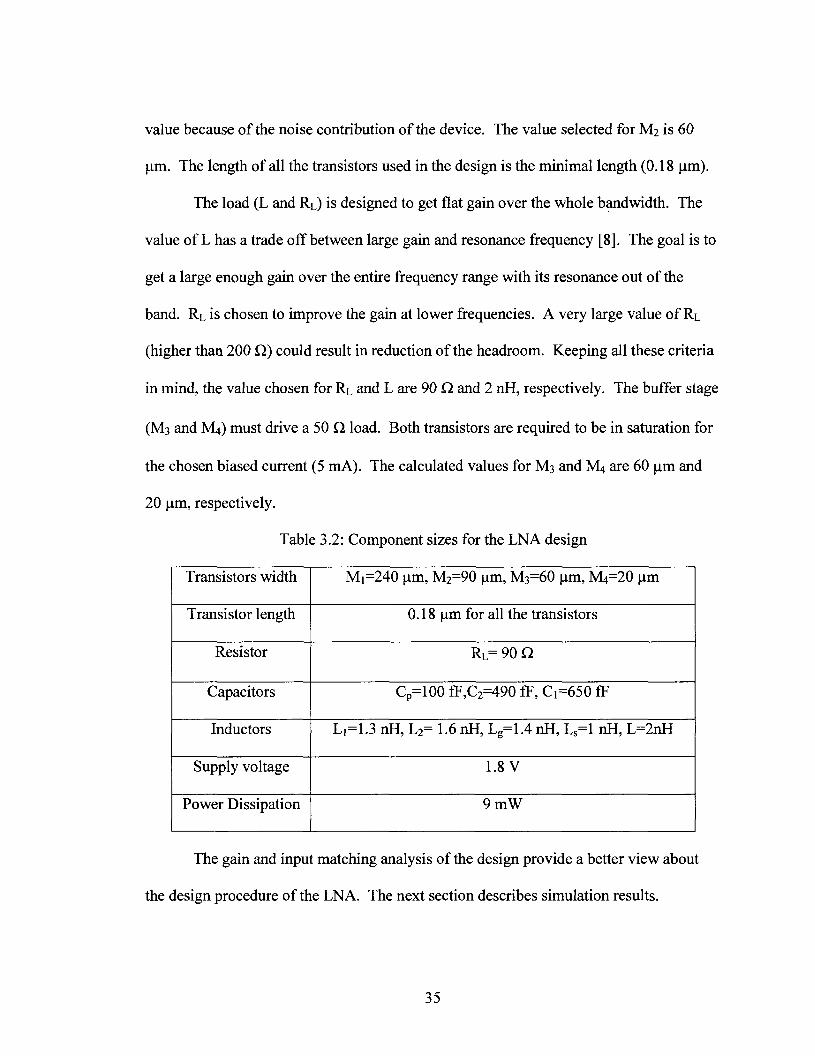
value because of the noise contribution of the device. The value selected for M2 is 60
um. The length of all the transistors used in the design is the minimal length (0.18 urn).
The load (L and RL) is designed to get flat gain over the whole bandwidth. The
value of L has a trade off between large gain and resonance frequency [8]. The goal is to
get a large enough gain over the entire frequency range with its resonance out of the
band. RL is chosen to improve the gain at lower frequencies. A very large value of RL
(higher than 200 Q) could result in reduction of the headroom. Keeping all these criteria
in mind, the value chosen for RL and L are 90 Q and 2 nH, respectively. The buffer stage
(M3 and M4) must drive a 50 Q load. Both transistors are required to be in saturation for
the chosen biased current (5 mA). The calculated values for M3 and M4 are 60 um and
20 um, respectively.
Table 3.2: Component sizes for the LNA design
Transistors width
Transistor length
Resistor
Capacitors
Inductors
Supply voltage
Power Dissipation
Mi=240 um, M2=90 um, M3=60 um, M4=20 um
0.18 um for all the transistors
RL= 90 Q
Cp=100 fF,C2=490 fF, Ci=650 fF
Li=1.3 nH, L2= 1.6 nH, Lg=1.4 nH, Ls=l nH, L=2nH
1.8V
9mW
The gain and input matching analysis of the design provide a better view about
the design procedure of the LNA. The next section describes simulation results.
35

3.3 Simulations and results
3.3.1 Gain vs. frequency simulation
AC Response
8G Freq (Hz)
10G
Figure 3.8: Gain vs. frequency simulation
As clearly seen from Figure 3.8, the circuit has a gain of 10 to 11 dB between the
frequency range of 3 to 10 GHz. The SpectreS simulator was used to simulate the gain
versus frequency chart. This design gives good gain over the entire UWB frequency
range because selection of the topology and the sizes of the components were correct. In
the inductor source degeneration topology (which is used in the design) the inductor is
connected between the source of Mi and ground provides the negative feedback. This
negative feedback is essential to stabilize the amplifier for the entire frequency range.
The phase margin for the design is approximately 40 degrees.
A two-port network is essential in RF design simulations. For the rest of the
simulations a two-port network design was used, the model of which is shown in Figure
3.9. Port 1 is the input port and Port 2 is the output port.
36

l l
AC(
ort 1 <
•
LNA
•< 12
AC(\
Port2|
Figure 3.9: LNA schematic with ports
3.3.2 Noise figure simulation
The noise figure is defined by amount of noise contributed by the circuit. For any
LNA design it is ideal to have our noise figure as low as possible. As mentioned in the
abstract, the targeted noise figure for this project was 4 dB and the design gives us a noise
figure of less than 4 dB for the entire UWB frequency band which is 3 GHz to 10 GHz.
The noise figure was simulated using the SpectreS simulator. An S-parameter simulation
window was used to achieve the plot show in Figure 3.10.
S-parameter Analysis NF mag
10G
Figure 3.10: Noise figure simulation
37

3.3.3 GA, GT and GP simulations
GA, GT and GP are different kinds of small signal gain simulations. There were
no set criteria as to what these results should be. GA stands for amplification gain, GT
stands for transducer gain and GP stands for power gain. Simulation steps similar to the
noise figure simulation in Section 3.3.2 were followed for the S-parameter simulations.
S-Parameter Response GA[dB]
GP[dB]
Freq (Hz)
3.11: GA, GT and GP simulation
3.3.4 1-dB compression curve
As described in Chapter 2, the 1-dB compression point is a good measure of the
linearity of the LNA. The Spectre simulator was used for the 1-dB compression and IIP3
point simulation, unlike the SpectreS simulator for the gain and noise figure simulations.
Periodic Steady State (PSS) response was the chosen analysis method. The plot shown in
38

Figure 3.12 was created using two tones, 8 GHz and 9 GHz. As seen in the Figure 3.12
the 1-dB compression point is -8 dB which is well within the range.
o.o
-10
-20
CO
3
-30
-40
-50 -40
Periodic Steady State Response
8 GHz tone
9 GHz tone
-30 -20 Prf (dBm)
1 dB Compression Point = -9.28 dB
-10 0.0
Figure 3.12: 1-dB compression point
3.3.5 IIP3 results
The IIP3 results were used to summarize the LNA linearity with two different
frequencies on the RF input. Figure 3.13 shows one such result. The two different
frequencies are 8 GHz and 9 GHz. Because of the LNA non-linearity, the 3rd order and
the 1st order harmonics of 8 GHz and 9 GHz, respectively, were produced at the output of
the LNA.
39

Periodic Steady state Analysis
-30 -20 -10 ' 0.0
Prf (dBm)
Figure 3.13: IIP3 simulations
Table 3.3 tabulates the comparison between target and achieved results.
Table 3.3: Comparison between targeted and achieved results
Gain
Sn Input Matching
Bandwidth
Noise figure
IIP3
Power dissipation
Targeted
>8dB
<-5dB
3-10 GHz
<5dB
-12 dB
<20mW
Achieved
1 0 - l l d B
<-5dB
3-10 GHz
3 -5dB
-10 dB
15.4 mW
40

It is evident from the Table 3.3 that most of the parameters were achieved as
predicted in Chapter 1. There is always a trade off amongst gain, noise and linearity in
RF circuits, and that is why the IIP3 is 2 dB off of the targeted value. The 1-dB
compression point and the IIP3 test were conducted at 8 GHz with a beat frequency of 1
GHz.
3.4 On-chip inductor using ADS
This section discusses the design and the analysis of on-chip spiral inductors. The
on-chip inductors have a significant effect in the design of the radio frequency integrated
circuits (RFICs), which can be modified to enhance the bandwidth of the system. This
section describes the design and optimization of the on-chip inductor.
The Figure 3.14 shows the spiral inductor-n model. In this model, L defines the
nominal inductance, and Rs defines the series resistance. The sheet resistance of the
metal layer can be used only for calculating the DC resistance of the spiral. The
resistance of the spiral increases at higher frequencies because of the skin effect and the
Eddy current effect. The skin effect is caused by the greater current flow near the surface
of the inductor than at its core. The Eddy current is caused by the induced current flow
into the lossy substrate. The series capacitance (Cs) results from the spacing capacitor
between the two inductor turns as well as from the capacitance between the spiral and the
metal under-pass. The oxide capacitance Coxi and COX2 presents the parasitic capacitor
between the substrate and inductor. The substrate resistance (Rsj) and capacitance (Csj) of
the silicon are shown in the inductor-n model.
41

Ideally, the adjacent turns are almost equipotential, so the effect of the interterm
fringing capacitance is neglected. However, there is a relatively large potential difference
between the spiral and the center-tap under-pass allowing this type of overlap capacitor to
be considered for use.
Portl L
A/W-Port 2
^ C 0 ^ox—r—
Rs Rsi'
Figure 3.14: The spiral inductor-TI model
The performance of an inductor is known as the Quality factor (Q), which is
expressed as:
Engergy Stored Q = 2TI = 9-77" * -
Energy Loss in one Oscillation Cycle (3.7)
where the energy stored is the difference between the peak magnetic energy Epeak (magnetic)
and the peak electric energy Epeak (electric) stored in any parasitic capacitance. At higher
frequencies, the energy dissipation occurs in the silicon substrate, which degrades the
inductor quality factor. As the inductor requires significant space on the chip, it is
susceptible to collecting and transmitting noise. Therefore, decoupling the inductor from
the substrate can improve the overall performance, improve the quality factor, enhance
42

isolation, and simplify modeling. The spiral inductor-Il model schematic and layout
were done in the Advanced Design Systems (ADS) tool as shown in the Figures 3.15 and
3.16, respectively.
. |f_^
o Port 1
Z=500 Ohm -±r
C=0.02 pF
L=3nH
C=100fF
R=48.5 Ohm
i
C=100fF U
Port 2
Z=500 Ohm
C=0.02 pF < R-6722 •S Ohm
• r
1 :=7158 _L Ohm "T" C=100fF
Figure 3.15: Pi-model generated in ADS
The substrate material used for the layout and the layer, which is being used to
fabricate the inductor, will determine the actual value of the inductor. Table 3.4 shows
parameters of the substrate that are used for the inductor layout in ADS.
Table 3.4: Substrate information of the inductor
Layer
Thickness (um)
Permittivity (Er)
Conductivity (Siemens/m)
Metal layer
0.5
-
2.8EU/
Silicon Dioxide
7
3.8
0
Silicon
400
0
10
43

Figure 3.16 shows the on-chip inductor used in the design. A metal layer is
chosen and it is laid out in a spiral fashion [9]. Any polygon shape can be used for the
design. A simple square design is chosen for all the layouts. Table 3.5 shows the
dimensions of all the inductors used in the LNA design.
Table 3.5: Inductor dimensions
Value
InH
2nH
1.6 nH
1.3 nH
1.4 nH
# ofturns
3.5
3.5
3.5
4
3.5
Turn spacing
1 um
2 urn
2 um
2 um
3 um
Turn width
2 um
4 um
2 um
2 um
2 um
Outer diameter
50 um
100 um
71 um
60 um
72 urn
Figure 3.16 is an image of a inductor of 1.6 nH. o
10 20 30 40 50 60 70
: _ 10
20
30
40
50
60
70
Figure 3.16: Inductor of 1.6 nH
44

The goal here was to simulate the inductor for its S-parameters and use those
results to generate the pi-model for every inductor in the design [10]. Figure 3.17 shows
the S-parameter result for the inductor in Figure 3.16.
The S-parameter result can be used to generate the pi-model using the "Spice
Model Generator" feature in the ADS tool. After opening the "Spice Model Generator",
it was necessary to browse the S-parameter result file and specify the name of the result
file. The result is a text file which looks like a table mentioning the values of the
resistors, capacitors and inductors of the pi-model.
S11 S22
freq (0,00Hz to 50GHz) freq (0.00Hz to 50GHz)
S12 S21
freq (O.OOHzto 50GHz) freq (00oHzto 50GHz)
Figure 3.17: S-parameter results for the spiral inductor
45

Next, the S-parameter results in Figure 3.17 were converted into the Z-
parameters in order to get the Q analysis of the inductor. Figure 3.18 shows the equations
that assisted in creating the Z-parameter.
gHzin7=1-S(2,2)
ggjzin3=1-S(2,2) Sf lz in5=1+S(2,2)
Hflzirt2=14*5(1,1) SBz in6=1-S(1 ' '1)
B f l Z_11=50*(zin11_num/zin_den) g f l zin1 1_num=(zin2*zin3)+(S(1,2)*S(2,1))
3 f l Z_22=50*(zin22_num/zin_den) g J J zin22_num=(zin6*zin5)+(S(1,2)*S(2,1))
B B Z_12=50*(2*S(1,2)/zin_den) [ 3 9 zin_den=(zin7*zin6)-(S(1,2)*S(2,1))
ggQ Z_21=50*(2*S(2,1)/zin_den)
B H Zin=Z_11 -((Z_12*Z_21 )/Z_22)
Figure 3.18: Generation of the Z-parameters in ADS
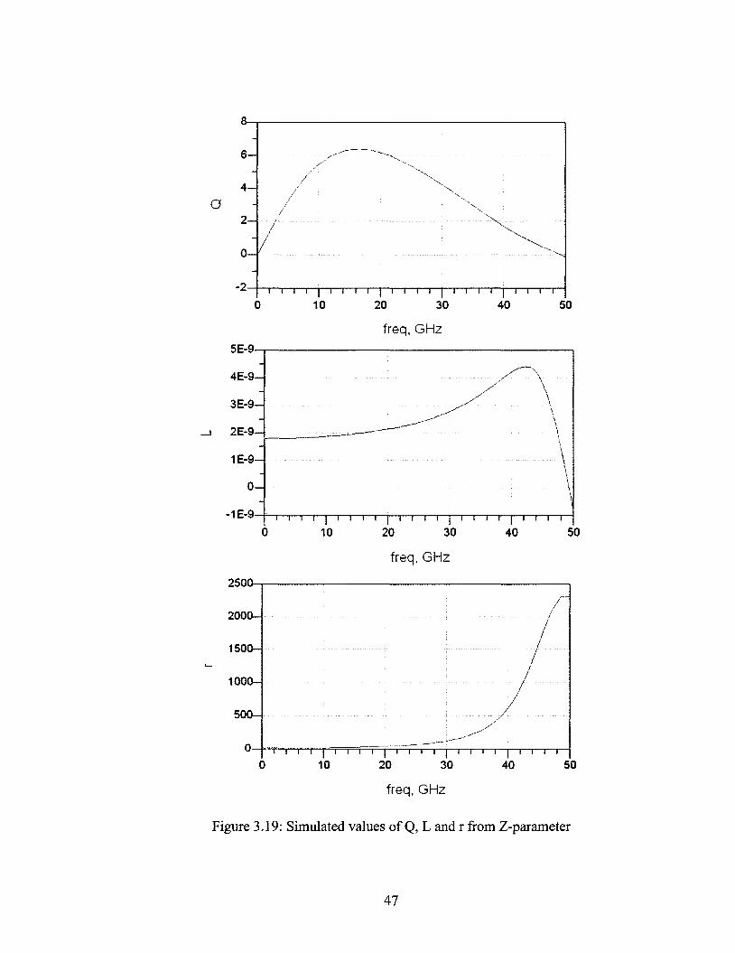
The actual values of L, r and Q can be obtained from the Z-parameters. Figure
3.19 shows the simulated values of L, r and Q for the inductor over the frequency from 0
to 50 GHz.
Table 3.6 shows a comparison between the simulated results before and after
inserting the pi-model. It was observed that there was slight degradation in the gain and
noise figure of the design. All the inductors were optimized for the area [11]. All the
parasitic parameters, which were not considered in the simulation without the pi-model,
come into affect when the pi-model was included in the LNA design. The insertion of
extra parasitics caused degradation in the gain and noise figure.
46
o
20 30 40
freq, GHz
freq. GHz
2500
freq, GHz
Figure 3.19: Simulated values of Q, L and r from Z-parameter
47

Table 3.6: Comparison of results before and after inserting pi-models for inductors
Gain
Sn Input Matching
Bandwidth
Noise figure
IIP3
1-dB compression point
Schematic with inductors
1 0 - l l d B
<-5dB
3-10 dB
3-5 dB
-10 dB
-8dB
Schematic with pi-models
7dB
<-6dB
3-10 dB
5-7 dB
-9dB
-8dB
3.5 Final layout and extraction
The layout of the entire schematic was done using Cadence's Virtuoso tool.
TSMC 0.18u technology has been used to design and implement the transistor level
design. The minimum channel length for this technology is 0.18 urn. Apart from the
inductor (which was discussed in the previous section), the schematic has 3 capacitors
and one resistor. A rectangle of poly layer was used to fabricate the resistor. The poly
layer makes a good resistor because of its high resistance and low parasitics. Rectangles
of the metal 1 and 2 layers were used to create capacitors of various values. Resistor IDs
and capacitor IDs were added to the resistors and capacitors to let the tool treat them as a
resistors and capacitors and not just any metal layer.
Figures 3.20 and 3.21 show the layout of the design and give an overall idea of
how the different components have been arranged in the layout. A Design Rule Check
48

(DRC) and a Layout Versus Schematic (LVS) comparison were performed on the layout.
The DRC checks for potential errors in the layout. The LVS checks the layout against
the schematic and verifies that all the nets are matching.
Vdd
Load resistance made of poly
* Output
35 micrometer
Figure 3.20: Layout without capacitors and inductors
After the DRC and LVS were completed successfully, layout extraction was done.
The extraction gives an overall idea about the parasitics of the design. Since the metal
layers 1 and 2 have been used, the design has quite a few parasitics. Special care has
been taken to implement them into the design.
49

Finally, post layout simulations were carried out to check the functionality of the
design. Table 3.7 shows a comparison between the simulated and extracted results.
15 E o o E
Vdd
533 micrometer -
Figure 3.21: Final layout
Table 3.7: Comparison between schematic and extracted simulations
Gain
Sn Input Matching
Bandwidth
Noise figure
IIP3
1-dB-compression point
Schematic simulation
10-11 dB
<-5dB
3-10 dB
3-5 dB
-10 dB
-8dB
Extracted simulation
7dB
<-6dB
3-10 dB
4-6 dB
-9dB
-9dB
50

The extracted results show little degradation in the gain and noise figure because
the design has large capacitors in it. Better matching of the capacitors would have given
results closer to the schematic results.
In summary, it could be said that a successful and functionally working LNA has
been designed for UWB application. Although there is some degradation in the result
parameters after extraction, the design still meets the specifications and is ready to be
tapped out. Table 3.8 presents a comparison of this work to other works in similar areas.
If one compares this thesis to other works presented in Table 3.8 one understands that the
proposed design has a significantly lower noise figure than other works.
Table 3.8: Summary of comparison of this work with past works in LNA
This
Work
[12]
[13]
[14]
[15]
[16]
Technology
0.18uCMOS
0.18uCMOS
0.18uCMOS
0.6u CMOS
0.6u CMOS
0.25u CMOS
SndB
<-5
<-9.9
<-8
<-7
<-6
<-8
*Jmax
dB
11
10.4
8.1
7.4
6
13
BGHz
3 - 1 0
2.4-9.5
0.6-22
0 .5 -4
1.5-7.5
0-1 .6
dB
3
4.2
4.3
5.4
8.7
3.9
HP3
dBm
-10
-8.8
N/A
N/A
N/A
N/A
"diss
mW
15.4
9
52
83
216
35
51

Chapter 4 Conclusion
The primary objective of the thesis was to design a Low Noise Amplifier (LNA)
that could be used for UWB applications. It was intended to have the LNA be capable of
providing enough gain within the frequency range 3 to 10 GHz with minimal noise.
In Chapter 1, various aspects of the UWB standard were studied. Chapter 2
explains LNA characterization along with presenting in-depth analysis of LNA gain,
noise, sensitivity, and linearity. Chapter 3 describes various useful and popular LNA
topologies. This chapter also gives good understanding of the proposed design,
schematic of the design, and simulated results. Chapter 3 also describes pi-model
generation of the inductor and illustrates the layout of the design.
The TSMC 0.18p. CMOS technology was used for the project. The LNA is
different from the conventional LNAs because it has a high pass band of 7.5 GHz. The
proposed design has a gain of 10 dB from 3 to 10 GHz after which it starts decreasing.
The target noise figure was less than 4 dB and simulations show that the proposed
architecture has succeeded in achieving that. The noise figure is well below 3 dB for the
entire frequency range.
Apart from those basic tests, the linearity of the design has been checked by using
the 1-dB compression point and IIP3 tests. The design has a -8 dB of 1-dB compression
point and -9dB of IIP3. The power supply voltage of TSMC 0.18|i technology is 1.8 V,
which plays a significant role in the generation of a design with low power dissipation.
Power dissipation for the proposed design is 15.4 watts.
52

The primary goal of any LNA is high gain with very low noise. Use of the ADS
generated pi-model is one of the reasons that the proposed design has such a low noise
figure. In comparing the schematic and extracted simulations, the input matching
parameter Sn is slightly different in the proposed design. Better matching of capacitors
in the input matching network could provide better Sn.
53

References
I] Technology demonstration of Freescale Semiconductor Inc., Tempe, Arizona.
2] UWB parameters for EMC coexistence with legacy systems, DAPRA, Jun 2003.
3] B. Razavi, RFMicroelectronics. Upper Saddle River, NJ: Prentice Hall, 1998.
4] T. H. Lee, The Design of CMOS Radio Frequency Integrated Circuits. New York: Cambridge University Press, 2000.
5] Chunyu Xin, "Radio frequency circuits for wireless receiver frond ends", M.S. Thesis, TAMU, Texas, 2004.
6] Institute for Infocomm Research, UWB Radio for wireless communications-12R 's perspectives, ASTAR.
7] Devendra K. Misra, Radio frequency and microwave communication circuits. Wiley, 2001.
8] Sunderarajan S. Mohan, "Modeling, design and optimization of on-chip inductors and transformers," Stanford University, June 9, 1999.
9] Stanford Microwave Integrated Circuit Laboratory, Available: Stanford Website, http://smirc.stanford.edu/spiralCalc.html.[Accessed: January,2006].
10] D. M. Pozar, Microwave Engineering. New York: Wiley, 1998.
II] Rokhsareh Zarnaghi, "Designing a CMOS ultra wide band low noise amplifier Considering Parasitic of Package," August 2005.
12] R. C. Liu, K.L. Deng and H. Wang, "A 0.6-22 GHz broadband CMOS distributed amplifier," IEEE J, Solid-State Circuits, Vol. 37, pp. 985-993, Aug. 2002.
13] Andrea Bevilacqua and Ali M. Niknejad, "An Ultrawideband CMOS Low-Noise Amplifier for 3.1 - 10.6 GHz Wireless Receivers," IEEE J, Solid-State Circuits, Vol. 39, pp. 2259-2268, Dec. 2004.
14] B. M. Ballweber, R. Gupta and D. J. Allstot, "A fully integrated 0.5-5.5-GHz CMOS distributed amplifier," IEEE J. Solid-State Circuits, Vol. 35 pp. 231-239, Feb. 2000.
15] H. T. Ahn and D. J. Allstot, "A 0.5-8.5-GHz fully dfferential CMOS distributed amplifier," IEEE J, Solid-State Circuits, Vol. 37, pp. 985-993, Aug. 2002.
54

[16] F. Bruccoleri, E. Klumperink, and B. Nauta, "Noise canceling in wideband CMOS LNAs," IEEE ISSCC Dig. Tech. Papers, 2002, pp. 406-407.
55
Related Documents