University of Tennessee, Knoxville University of Tennessee, Knoxville TRACE: Tennessee Research and Creative TRACE: Tennessee Research and Creative Exchange Exchange Masters Theses Graduate School 5-2007 Design and Analysis of a General Purpose Operational Amplifier Design and Analysis of a General Purpose Operational Amplifier for Extreme Temperature Operation for Extreme Temperature Operation Chandradevi Ulaganathan University of Tennessee - Knoxville Follow this and additional works at: https://trace.tennessee.edu/utk_gradthes Part of the Electrical and Computer Engineering Commons Recommended Citation Recommended Citation Ulaganathan, Chandradevi, "Design and Analysis of a General Purpose Operational Amplifier for Extreme Temperature Operation. " Master's Thesis, University of Tennessee, 2007. https://trace.tennessee.edu/utk_gradthes/327 This Thesis is brought to you for free and open access by the Graduate School at TRACE: Tennessee Research and Creative Exchange. It has been accepted for inclusion in Masters Theses by an authorized administrator of TRACE: Tennessee Research and Creative Exchange. For more information, please contact [email protected].

Welcome message from author
This document is posted to help you gain knowledge. Please leave a comment to let me know what you think about it! Share it to your friends and learn new things together.
Transcript
University of Tennessee, Knoxville University of Tennessee, Knoxville
TRACE: Tennessee Research and Creative TRACE: Tennessee Research and Creative
Exchange Exchange
Masters Theses Graduate School
5-2007
Design and Analysis of a General Purpose Operational Amplifier Design and Analysis of a General Purpose Operational Amplifier
for Extreme Temperature Operation for Extreme Temperature Operation
Chandradevi Ulaganathan University of Tennessee - Knoxville
Follow this and additional works at: https://trace.tennessee.edu/utk_gradthes
Part of the Electrical and Computer Engineering Commons
Recommended Citation Recommended Citation Ulaganathan, Chandradevi, "Design and Analysis of a General Purpose Operational Amplifier for Extreme Temperature Operation. " Master's Thesis, University of Tennessee, 2007. https://trace.tennessee.edu/utk_gradthes/327
This Thesis is brought to you for free and open access by the Graduate School at TRACE: Tennessee Research and Creative Exchange. It has been accepted for inclusion in Masters Theses by an authorized administrator of TRACE: Tennessee Research and Creative Exchange. For more information, please contact [email protected].
To the Graduate Council:
I am submitting herewith a thesis written by Chandradevi Ulaganathan entitled "Design and
Analysis of a General Purpose Operational Amplifier for Extreme Temperature Operation." I have
examined the final electronic copy of this thesis for form and content and recommend that it be
accepted in partial fulfillment of the requirements for the degree of Master of Science, with a
major in Electrical Engineering.
Benjamin J. Blalock, Major Professor
We have read this thesis and recommend its acceptance:
Charles L. Britton, Syed K. Islam
Accepted for the Council:
Carolyn R. Hodges
Vice Provost and Dean of the Graduate School
(Original signatures are on file with official student records.)
To the Graduate Council:
I am submitting herewith a thesis written by Chandradevi Ulaganathan entitled “Design
and Analysis of a General Purpose Operational Amplifier for Extreme Temperature
Operation.” I have examined the final electronic copy of this thesis for form and content
and recommend that it be accepted in partial fulfillment of the requirements for the
degree of Master of Science, with a major in Electrical Engineering.
Benjamin J. Blalock, Major Professor
We have read this thesis
and recommend its acceptance:
Charles L. Britton
Syed K. Islam
Accepted for the Council:
Carolyn Hodges
Vice Provost and Dean of the Graduate
School
(Original signatures are on file with official student records.)
DESIGN AND ANALYSIS OF A GENERAL PURPOSE
OPERATIONAL AMPLIFIER FOR EXTREME TEMPERATURE
OPERATION
A Thesis Presented for the
Master of Science Degree
The University of Tennessee, Knoxville
Chandradevi Ulaganathan
May 2007
This thesis is dedicated to my parents,
Smt. Saroja Ulaganathan and Shri. Ulaganathan,
my friend Aparna Thyagarajan and the rest of my family
for always inspiring and encouraging me to see my dreams come true
ii
ACKNOWLEDGEMENTS
I would like to express my sincere gratitude to my advisor Dr. Benjamin J.
Blalock whose constant guidance, support and patience helped me in completing this
thesis. I wish to thank my thesis committee members Drs. Charles L. Britton and Syed K.
Islam for their helpful suggestions and support in this work.
I am especially grateful to Dr. Dayakar Penumadu for offering invaluable
guidance and financial support in the initial stage of my Masters work. I would like to
thank all my colleagues in the Integrated Circuits and Systems Laboratory (ICASL) for
their support. I am indebted to Neena Nambiar and Suheng Chen for the priceless
discussions, suggestions and their inspiration.
I thank my parents Smt. Saroja Ulaganathan and Shri. Ulaganathan, and my
sisters Aarthi and Vaishnavi, for their unconditional support and faith in me. I am grateful
to my friends – Aparna, Sangeetha, Ezhil, Juhee, Anton and others for their support and
encouragement.
This work was funded by the NASA Exploration Technology Development
Program (ETDP). Special appreciation is extended to our collaborators, including Prof.
John Cressler’s team at Georgia Tech.
iii
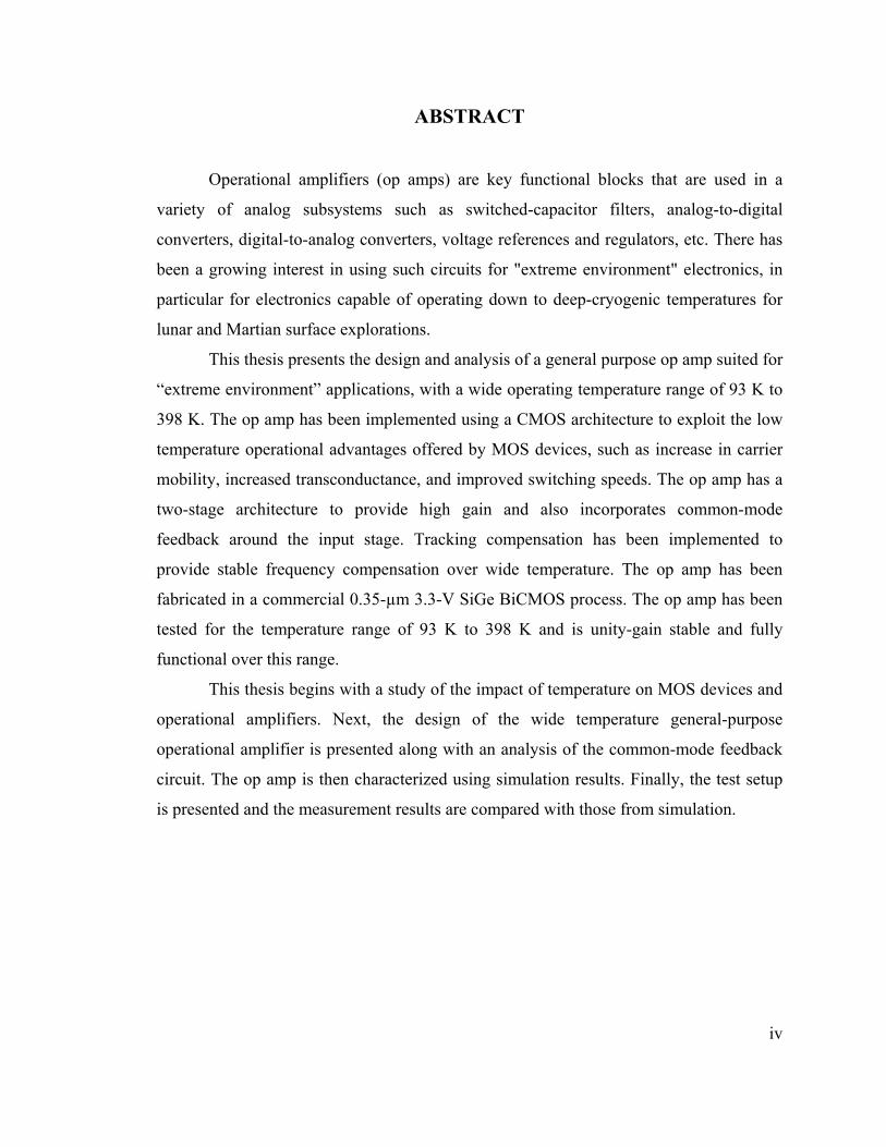
ABSTRACT
Operational amplifiers (op amps) are key functional blocks that are used in a
variety of analog subsystems such as switched-capacitor filters, analog-to-digital
converters, digital-to-analog converters, voltage references and regulators, etc. There has
been a growing interest in using such circuits for "extreme environment" electronics, in
particular for electronics capable of operating down to deep-cryogenic temperatures for
lunar and Martian surface explorations.
This thesis presents the design and analysis of a general purpose op amp suited for
“extreme environment” applications, with a wide operating temperature range of 93 K to
398 K. The op amp has been implemented using a CMOS architecture to exploit the low
temperature operational advantages offered by MOS devices, such as increase in carrier
mobility, increased transconductance, and improved switching speeds. The op amp has a
two-stage architecture to provide high gain and also incorporates common-mode
feedback around the input stage. Tracking compensation has been implemented to
provide stable frequency compensation over wide temperature. The op amp has been
fabricated in a commercial 0.35-µm 3.3-V SiGe BiCMOS process. The op amp has been
tested for the temperature range of 93 K to 398 K and is unity-gain stable and fully
functional over this range.
This thesis begins with a study of the impact of temperature on MOS devices and
operational amplifiers. Next, the design of the wide temperature general-purpose
operational amplifier is presented along with an analysis of the common-mode feedback
circuit. The op amp is then characterized using simulation results. Finally, the test setup
is presented and the measurement results are compared with those from simulation.
iv
TABLE OF CONTENTS
CHAPTER 1 INTRODUCTION................................................................................. 1
1.1 Motivation .................................................................................... 1
1.2 Scope of the Thesis....................................................................... 2
1.3 Organization of the Thesis............................................................ 3
CHAPTER 2 IMPACT OF TEMPERATURE ON ELECTRONICS..................... 4
2.1 Operational Amplifiers – Fundamentals ...................................... 4
2.2 Effect of Temperature Variation .................................................. 5
2.2.1 Effect on MOS devices ....................................................... 5
2.2.2 Effect on Op amp circuits ................................................. 12
CHAPTER 3 DESIGN OF THE WIDE TEMPERATURE RANGE GENERAL-
PURPOSE OP AMP ....................................................................................................... 14
3.1 Op amp Architecture .................................................................. 14
3.1.1 Input Stage ........................................................................ 14
3.1.2 Output Stage...................................................................... 16
3.2 Complete Schematic................................................................... 18
3.2.1 Open-loop Gain................................................................. 19
3.2.2 Frequency Compensation.................................................. 20
3.2.3 Input common mode range ............................................... 22
3.2.4 Noise ................................................................................. 23
3.2.5 Offset Voltage................................................................... 24
3.2.6 Output Swing .................................................................... 26
3.2.7 Slew Rate .......................................................................... 26
3.2.8 Common-mode Feedback (CMFB) .................................. 27
3.2.9 Current Reference ............................................................. 32
3.3 Simulation Results...................................................................... 33
3.4 Layout and Implementation........................................................ 40
v
CHAPTER 4 WIDE TEMPERATURE RANGE GENERAL-PURPOSE OP
AMP – MEASUREMENT RESULTS .......................................................................... 42
4.1 Temperature Testing................................................................... 42
4.2 Test Setup ................................................................................... 43
4.3 Summary..................................................................................... 57
CHAPTER 5 CONCLUSIONS ................................................................................. 58
5.1 Conclusions ................................................................................ 58
5.2 Future Work................................................................................ 58
5.2.1 Circuit-level ...................................................................... 58
5.2.2 System-level...................................................................... 59
REFERENCES ............................................................................................................... 60
APPENDIX ............................................................................................................... 65
A.1 Calculation of Open-loop Gain .................................................. 66
A.2 Calculation of Input Referred Noise Voltage............................. 67
A.3 Derivation of the Loop Gain of CMFB Circuit.......................... 69
A.4 Test Board .................................................................................. 72
VITA ............................................................................................................... 73
vi

TABLE OF TABLES
Table 1.1 - Op amp Specifications...................................................................................... 3
vii
TABLE OF FIGURES
Figure 2.1 - Basic operational amplifier ............................................................................. 5 Figure 2.2 - Simple two-stage CMOS op amp.................................................................. 12 Figure 3.1 - Input stage of the op amp.............................................................................. 15 Figure 3.2 - The output stage along with input stage and CMFB block diagram [28] ..... 16 Figure 3.3 - Complete schematic of the op amp ............................................................... 19 Figure 3.4 - Common-mode feedback circuit along with the input stage......................... 28 Figure 3.5 - Simulated frequency response of CMFB circuit ........................................... 30 Figure 3.6 - CMFB transient response for (a) common-mode signal and (b) differential-mode signal ....................................................................................................................... 31 Figure 3.7 - Plot showing the difference voltage at output of input stage vs. bias current32 Figure 3.8 - Schematic of constant IC current reference circuit [35] ............................... 33 Figure 3.9 - Simulation result for ICMR across temperature ........................................... 34 Figure 3.10 - Simulation result for open-loop gain and phase across temperature........... 35 Figure 3.11 - Simulation result for small-signal rise time across temperature ................. 35 Figure 3.12 - Simulation result for small-signal fall time across temperature.................. 36 Figure 3.13 - Simulated positive slewing edge across temperature.................................. 36 Figure 3.14 - Simulated negative slewing edge across temperature................................. 37 Figure 3.15 - Simulated input referred noise voltage across temperature ........................ 38 Figure 3.16 - Simulation result for PSRR across temperature.......................................... 38 Figure 3.17 - Simulation result for CMRR across temperature ........................................ 39 Figure 3.18 - Simulation result for constant IC current reference .................................... 39 Figure 3.19 - Layout of the general-purpose op amp........................................................ 41 Figure 3.20 - Die photo of the general-purpose op amp ................................................... 41 Figure 4.1- Setup for temperature testing ......................................................................... 42 Figure 4.2 - Measurement setup for offset voltage ........................................................... 44 Figure 4.3 - Measured VOS across temperature................................................................. 44 Figure 4.4 - Measurement setup for ICMR....................................................................... 45 Figure 4.5 - Measured ICMR max across temperature..................................................... 46 Figure 4.6 - Open-loop gain measurement circuit ............................................................ 47 Figure 4.7 - Measured results for open-loop gain across temperature.............................. 47 Figure 4.8 - Measured UGBW across temperature........................................................... 49 Figure 4.9 - Measured UGBW across temperature using sinusoidal input signal ............ 49 Figure 4.10 - Measured phase margin across temperature ............................................... 50 Figure 4.11 - Measured positive slewing edge across temperature .................................. 51 Figure 4.12 - Measured negative slewing edge across temperature ................................. 51 Figure 4.13 - Measured slew rate across temperature....................................................... 52 Figure 4.14 - Setup for noise measurement ...................................................................... 53 Figure 4.15 - Measured input referred noise voltage across temperature......................... 53 Figure 4.16 - PSRR measurement circuit ......................................................................... 54 Figure 4.17 - Measured PSRR across temperature ........................................................... 55 Figure 4.18 - CMRR measurement circuit........................................................................ 56 Figure 4.19 - Measured CMRR across temperature ......................................................... 56 Figure 4.20 - Measured bias current vs. temperature........................................................ 57
viii
Figure A.1 - Setup to determine the flicker noise corner frequency................................. 67 Figure A.2 - Small-signal equivalent of the CMFB’s ac half-circuit ............................... 70 Figure A.3 - Picture of Test Board.................................................................................... 72
ix
Chapter 1 Introduction
1.1 Motivation
Operational amplifiers (op amps) are versatile devices used as key functional
blocks in a variety of high-precision analog/mixed-signal systems. Its application spans
the broad electronic industry filling requirements for signal conditioning, special transfer
functions, analog instrumentation, analog computation and special systems design [1].
There continues to be a growing interest in developing SoC (System-on-Chip) integrated
systems for use in numerous applications. These applications often place challenging
constraints in the design of various electronic components. “Extreme environments”
represent a class of niche electronic applications wherein the electronic components must
operate in an environment that is outside the domain of commercial or military
specifications. This would include temperatures above or below the standard military
specification, in a radiation intensive environment such as space, in a high vibration
environment, in a high (low) pressure environment, or even in a caustic or chemically
corrosive environment as inside the human body [2].
In this thesis, extreme temperature effects on electronics have been studied and a
robust operational amplifier that works across a wide temperature range has been
designed, fabricated and tested. With the recent development of low temperature
electronics to support space exploration, this work is targeted at the moon’s surface
environment where the ground temperature swings up to 393 K (120 °C) during the day
and down to 93 K (-180 °C) during the night.
At present, robotic exploration rovers [3] have all the essential parts that control
the system, such as electronics, batteries and computers operating in a temperature
controlled environment of a warm electronic box (WEB). The temperature in the WEB is
maintained to be within the operating range of all the enclosed components in order to
guarantee their reliable operation. Heaters, thermostats, heat switches and gold paint help
maintain the temperature inside the WEB, but they increase the system’s power
consumption, size and mass [3]. The use of warm boxes also mandates a centralized
1
architecture wherein the control signals are generated in the WEB and communicated to
various parts of the rover through wiring cables, thus reducing reliability. By developing
electronic components that are capable of reliable operation under extreme conditions
without a “warm box”, a distributed architecture can be realized. The result would be
reduced power consumption and the launch weight while the reliability, vehicle form
factor, safety and mission cost are also dramatically improved [4].
With this motivation, the goal of this work is to develop an operational amplifier
that functions well under extreme temperatures. This would help in designing remote
electronic systems for robotic rovers and other spacecraft that provide data acquisition
and control for various applications.
1.2 Scope of the Thesis
The purpose of this work is to design an operational amplifier that can operate in
extreme environments. Specifically, the op amp is targeted to serve as a general purpose
building block in high-precision analog signal conditioning systems. There are several
parameters that characterize an op amp. Some key parameters include gain, gain-
bandwidth, slew rate, input common-mode range (ICMR), common-mode rejection ratio
(CMRR), power-supply rejection ratio (PSRR), output swing, offset voltage, noise and
power consumption. Depending on the system specification, some characteristics are
given more precedence over others. For this work, it is important that the gain, gain-
bandwidth, output swing, noise and offset voltage are maintained at an acceptable level
across temperature. The op amp is fabricated in a 0.35-µm 3.3-V SiGe BiCMOS process.
Table 1.1 presents a list of requirements set for the design of this general purpose op amp.
An all-CMOS approach is used for this work to provide the opportunity to study and
analyze the impact of temperature variation on MOS devices and its influence on op amp
performance. An analysis of the common-mode feedback circuitry implemented in the
differential input stage of the op amp is also performed.
2
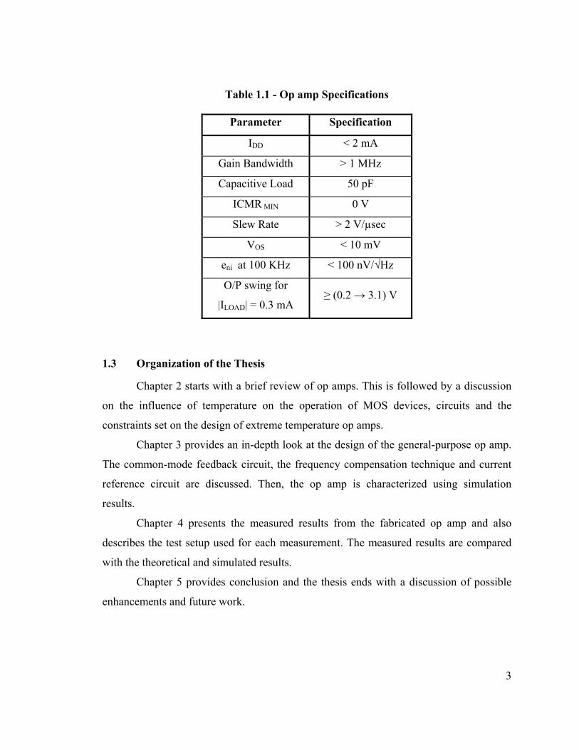
Table 1.1 - Op amp Specifications
Parameter Specification
IDD < 2 mA
Gain Bandwidth > 1 MHz
Capacitive Load 50 pF
ICMR MIN 0 V
Slew Rate > 2 V/µsec
VOS < 10 mV
eni at 100 KHz < 100 nV/√Hz
O/P swing for
|ILOAD| = 0.3 mA ≥ (0.2 → 3.1) V
1.3 Organization of the Thesis
Chapter 2 starts with a brief review of op amps. This is followed by a discussion
on the influence of temperature on the operation of MOS devices, circuits and the
constraints set on the design of extreme temperature op amps.
Chapter 3 provides an in-depth look at the design of the general-purpose op amp.
The common-mode feedback circuit, the frequency compensation technique and current
reference circuit are discussed. Then, the op amp is characterized using simulation
results.
Chapter 4 presents the measured results from the fabricated op amp and also
describes the test setup used for each measurement. The measured results are compared
with the theoretical and simulated results.
Chapter 5 provides conclusion and the thesis ends with a discussion of possible
enhancements and future work.
3
Chapter 2 Impact of Temperature on
Electronics
Chapter 2 presents a discussion on the effects of temperature on MOS devices and
op amp circuit performance. This discussion begins with briefly reviewing the essential
components that make up an op amp and characterizing an op amp using the parameters
that dictate its performance.
2.1 Operational Amplifiers – Fundamentals
Ideal operational amplifiers are functional blocks that have infinite voltage gain
over an infinite bandwidth, infinite input resistance and zero output resistance. In
practice, op amps only approach these ideal characteristics. They use negative feedback
to establish and control a closed-loop transfer function that is stable and independent of
the open-loop gain of the op amp. Figure 2.1 presents a functional block diagram of a
basic operational amplifier. The differential input stage provides the required high gain
for the op amp and can also perform the differential-input to single-ended output
conversion. The second stage is usually an inverting stage and can offer high gain as well
as differential-to-single ended conversion if necessary. Op amps that need to drive small
resistive loads also include a buffer/output stage that drives the load and determines the
output swing. The compensation circuitry ensures frequency stability when the op amp is
used in a negative feedback network. The biasing circuitry provides a stable, quiescent
operating point for the entire circuit. Op amps with different levels of complexity are
used in many applications and it is important to understand the parameters used in
evaluating these op amps. A brief review of the op amp parameters is included here.
The dynamic range of an op amp is controlled by the op amp’s offset voltage,
noise, input common-mode range (ICMR) and output swing. The ability of the op amp to
provide an accurate closed-loop gain is dictated by the open-loop gain (AOL). The
frequency response of the circuit is characterized by the small-signal bandwidth, phase
4
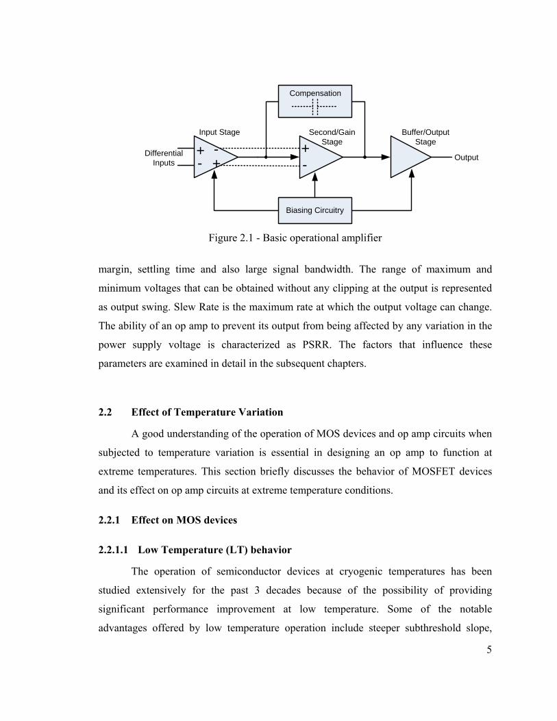
Compensation
-+
+-+
-
Biasing Circuitry
Differential Inputs
Output
Input Stage Buffer/Output Stage
Second/Gain Stage
Figure 2.1 - Basic operational amplifier
margin, settling time and also large signal bandwidth. The range of maximum and
minimum voltages that can be obtained without any clipping at the output is represented
as output swing. Slew Rate is the maximum rate at which the output voltage can change.
The ability of an op amp to prevent its output from being affected by any variation in the
power supply voltage is characterized as PSRR. The factors that influence these
parameters are examined in detail in the subsequent chapters.
2.2 Effect of Temperature Variation
A good understanding of the operation of MOS devices and op amp circuits when
subjected to temperature variation is essential in designing an op amp to function at
extreme temperatures. This section briefly discusses the behavior of MOSFET devices
and its effect on op amp circuits at extreme temperature conditions.
2.2.1 Effect on MOS devices
2.2.1.1 Low Temperature (LT) behavior
The operation of semiconductor devices at cryogenic temperatures has been
studied extensively for the past 3 decades because of the possibility of providing
significant performance improvement at low temperature. Some of the notable
advantages offered by low temperature operation include steeper subthreshold slope,
5
substantial increase in carrier mobility and saturation velocity, higher transconductance,
reduced thermal noise, increased thermal conductivity, improved reliability through
latch-up immunity, decrease in leakage current, and reduction of thermally activated
failure processes [8, 9, 10]. Operation at low temperature is challenged by the increase in
threshold voltage, increased susceptibility to hot carrier degradation effects and impurity
carrier freeze-out resulting in kink phenomenon and transient behavior of drain current at
cryogenic temperatures [10].
2.2.1.2 High Temperature (HT) behavior
Study of high temperature electronics is mainly driven by industrial applications
in geothermal sensors, space exploration and aircraft/automobile engine monitors [18 -
21]. The limitations of HT operation are primarily due to lowering of mobility and thus a
reduction in transconductance, increase in leakage currents, latch-up and reduced
reliability of the oxide layer, metal interconnects and packaging [22].
The parameters that are altered due to temperature variation have a major
influence on device performance. These parameters are discussed here.
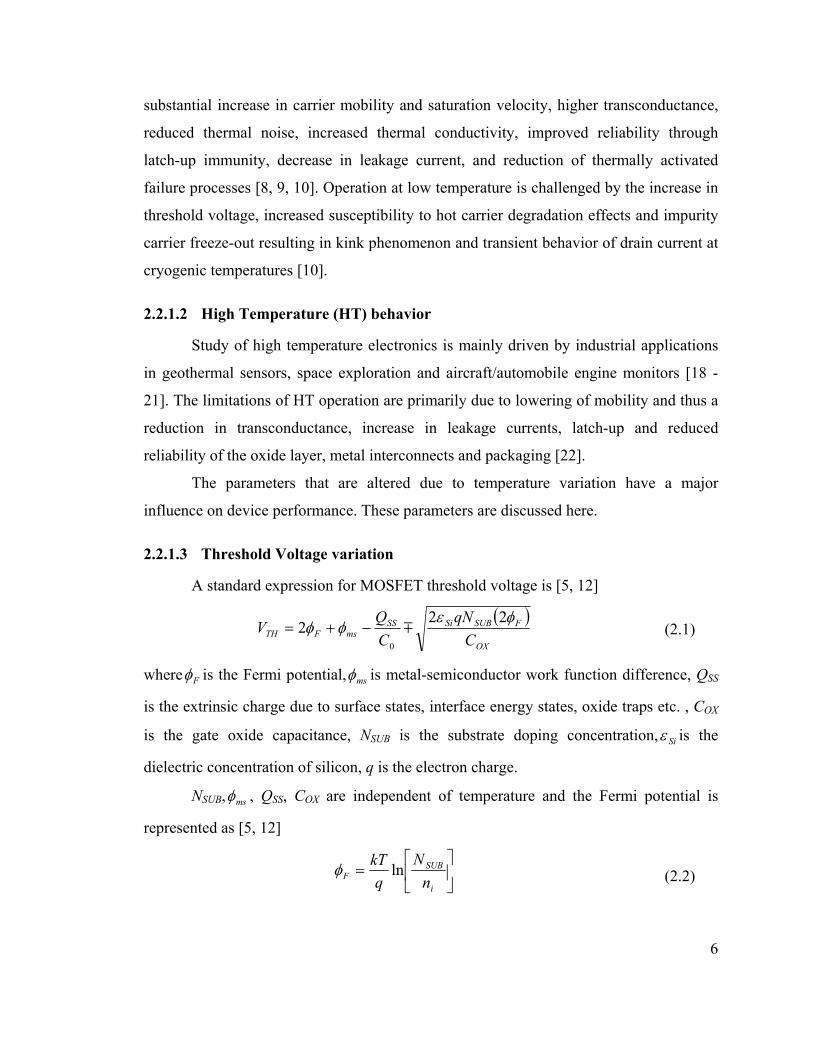
2.2.1.3 Threshold Voltage variation
A standard expression for MOSFET threshold voltage is [5, 12]
( )OX
FSUBSiSSmsFTH C
qNCQ
Vφε
φφ22
20
m−+= (2.1)
where Fφ is the Fermi potential, msφ is metal-semiconductor work function difference, QSS
is the extrinsic charge due to surface states, interface energy states, oxide traps etc. , COX
is the gate oxide capacitance, NSUB is the substrate doping concentration, Siε is the
dielectric concentration of silicon, q is the electron charge.
NSUB, msφ , QSS, COX are independent of temperature and the Fermi potential is
represented as [5, 12]
⎥⎦
⎤⎢⎣
⎡=
i
SUBF n
Nq
kT lnφ (2.2)
6
which is dependent on temperature. With a reduction in temperature, the intrinsic carrier
concentration, ni, reduces and the Fermi potential, Fφ , increases, hence the threshold
voltage increases at LT. In analog circuits the increase in VTH at LT reduces the dynamic
range of the circuit. Thus in an op amp, the ICMR would be reduced [13]. For the
BiCMOS fabrication process used here, the VTH of NMOS and PMOS devices vary
approximately 200 mV across the temperature range of −180 °C to 125 °C.
2.2.1.4 Mobility Variations
The carrier mobility variation across temperature presents a major constraint on
circuits operating across extreme temperature ranges. At LT mobility may increase by a
factor of 4 to 6, while at HT mobility decreases. The factors controlling mobility would
help in understanding this temperature dependence. The carrier mobility µ is controlled
by various scattering mechanisms like lattice scattering, ionized impurity scattering and
vertical field dependent surface scattering [14]. These mechanisms, and thus µ are a
function of applied electric field, temperature, channel impurity concentration and the
oxide layer thickness.
At room temperature, for small gate voltages, surface scattering is relatively
unimportant, so the surface mobility can approach bulk mobility. As gate voltage
increases, inversion layer carriers are subjected to increased electric field and are pushed
toward the surface, causing surface scattering to become more significant and lowers
mobility [14].
As temperature is lowered to near liquid nitrogen temperature (LNT) of about 77
K, the reduction in the lattice vibration makes lattice scattering less significant.
Therefore, mobility increases with reduction in temperature. The extent of this
enhancement depends on other factors influencing mobility. For instance, in transistors
with light doping near the surface, surface scattering effects dominate and mobility
depends strongly on vertical field applied. For such devices, the enhancement in mobility
at LNT over 27 °C is large for low vertical fields and less for higher fields [14]. Also,
devices built in wells are expected to have lower mobility at all temperatures and less µ
enhancement since ionized impurity scattering, which is independent of the magnitude of
7
vertical field, is significant at all temperatures [14].
The dependence of mobility as a function of temperature can be represented as
[10] α
μμ−
⎥⎦
⎤⎢⎣
⎡=
00 T
T (2.3)
where α is a constant that describes the temperature dependence and approximated as 1.3
for electrons and 1.2 for holes for a 0.5-µm CMOS technology.
The transconductance, gm, for inversion-mode MOSFETs is proportional to the
drift velocity in the channel and thus to the carrier mobility. Therefore, the variations in μ
across temperature affect the transconductance and thus the gain and bandwidth of
circuits.
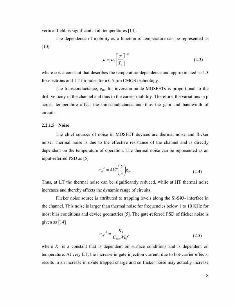
2.2.1.5 Noise
The chief sources of noise in MOSFET devices are thermal noise and flicker
noise. Thermal noise is due to the effective resistance of the channel and is directly
dependent on the temperature of operation. The thermal noise can be represented as an
input-referred PSD as [5]
mni gkTe ⎟⎠⎞
⎜⎝⎛=
3242 (2.4)
Thus, at LT the thermal noise can be significantly reduced, while at HT thermal noise
increases and thereby affects the dynamic range of circuits.
Flicker noise source is attributed to trapping levels along the Si-SiO2 interface in
the channel. This noise is larger than thermal noise for frequencies below 1 to 10 KHz for
most bias conditions and device geometries [5]. The gate-referred PSD of flicker noise is
given as [14]
WLfCKe
OXnif
12 = (2.5)
where K1 is a constant that is dependent on surface conditions and is dependent on
temperature. At very LT, the increase in gate injection current, due to hot-carrier effects,
results in an increase in oxide trapped charge and so flicker noise may actually increase
8
slightly [15]. Hence for low frequency applications where flicker noise is dominant, the
noise might not always reduce with a decrease in temperature. At HT there is an increase
in the thermal as well as the flicker noise.
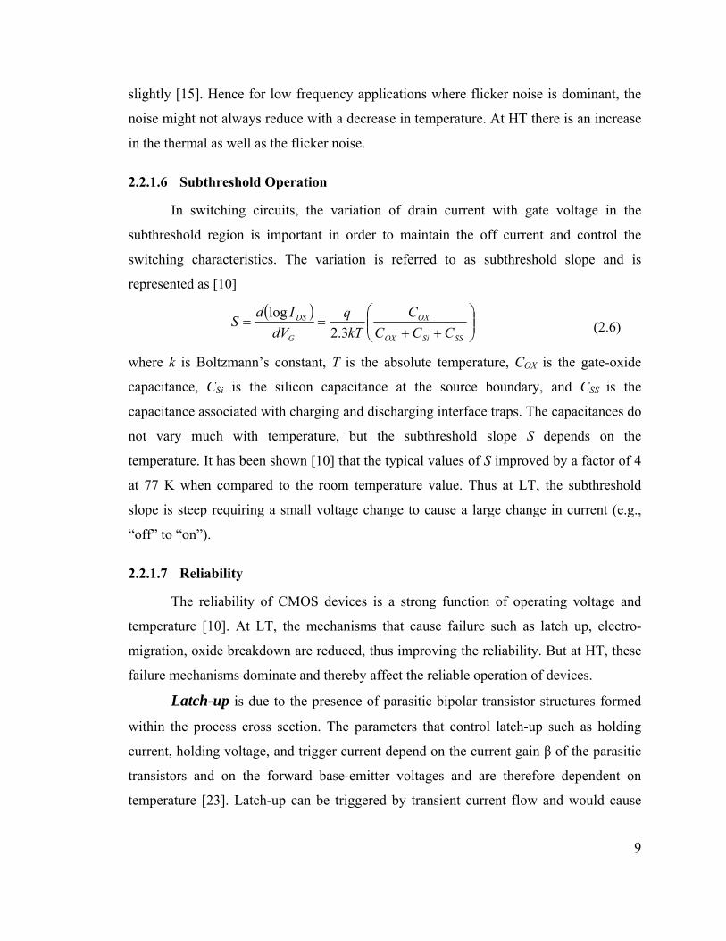
2.2.1.6 Subthreshold Operation
In switching circuits, the variation of drain current with gate voltage in the
subthreshold region is important in order to maintain the off current and control the
switching characteristics. The variation is referred to as subthreshold slope and is
represented as [10]
( )⎟⎟⎠
⎞⎜⎜⎝
⎛++
==SSSiOX
OX
G
DS
CCCC
kTq
dVId
S3.2
log (2.6)
where k is Boltzmann’s constant, T is the absolute temperature, COX is the gate-oxide
capacitance, CSi is the silicon capacitance at the source boundary, and CSS is the
capacitance associated with charging and discharging interface traps. The capacitances do
not vary much with temperature, but the subthreshold slope S depends on the
temperature. It has been shown [10] that the typical values of S improved by a factor of 4
at 77 K when compared to the room temperature value. Thus at LT, the subthreshold
slope is steep requiring a small voltage change to cause a large change in current (e.g.,
“off” to “on”).
2.2.1.7 Reliability
The reliability of CMOS devices is a strong function of operating voltage and
temperature [10]. At LT, the mechanisms that cause failure such as latch up, electro-
migration, oxide breakdown are reduced, thus improving the reliability. But at HT, these
failure mechanisms dominate and thereby affect the reliable operation of devices.
Latch-up is due to the presence of parasitic bipolar transistor structures formed
within the process cross section. The parameters that control latch-up such as holding
current, holding voltage, and trigger current depend on the current gain β of the parasitic
transistors and on the forward base-emitter voltages and are therefore dependent on
temperature [23]. Latch-up can be triggered by transient current flow and would cause
9
failure by the positive feedback action in the parasitic BJTs [16]. At LT the gain of BJTs
is very low such that the total gain in the parasitic BJTs is less than unity and thus latch-
up is suppressed. But at HT the increase in β enhances the likelihood of latch-up to occur.
Electro-migration, caused by the creation of metal voids and shorts in metal
interconnects due to the movement of metal atoms at high current densities, has a thermal
activation process. So at LT electro-migration is significantly reduced, but at HT electro-
migration reduces reliable circuit operation.
Hot carrier degradation effects: When high electric field is applied, the
carriers gain high kinetic energy and may be injected into the gate oxide and become
trapped there. This changes the MOSFET’s threshold voltage and transconductance. At
LT the reduced lattice scattering due to lattice vibrations results in a large fraction of
carriers reaching the gate and a high susceptibility to hot carrier degradation. At -180 °C
(77 K), there is an increase in these effects. This augmentation is not due to the enhanced
trapping in oxide, but due to increased influence of trapped charge on device operation
[10]. The degradation can be controlled by operating the devices with lower voltages and
thus placing a design constraint on the gate voltage [10].
2.2.1.8 Carrier Freeze-out
At and above room temperature, essentially all the impurity atoms are thermally
ionized and the concentration of mobile carriers is equal to the dopant concentration. As
temperature decreases, the Fermi level approaches the valence band causing the mobile
carriers to begin to freeze-out on the impurities and a corresponding decrease in electrical
conductivity is observed [11]. The carrier freeze-out situation at the semiconductor
surface under the gate is different than that in the bulk due to band bending [11]. The
electric field of the channel interface depletion region sweeps out any mobile carriers and
maintains complete ionization even at low temperatures. Approaching LNT carriers in the
bulk begin to freeze-out, but there is essentially no effect on the ionized impurity
concentration in the depletion region [11]. At strong freeze-out conditions of temperature
below 30K, kink effect and transient phenomenon on I-V characteristics are observed.
Kink effect: At LT when impurity freeze-out occurs, the MOS devices in
10
saturation region experience kink effect that is attributed to self-polarization of the
substrate due to the flow of majority carriers from body to source. The impurity freeze-
out in the bulk leads to a strong increase of the back resistance which prevents the
collection of drain impact ionization current through the body contacts. This results in a
self biasing of the body and the source-body junction becomes forward biased. This
causes a change in the threshold voltage and produces leveling of the drain current in
saturation resulting in a kink in the I-V characteristics [9].
Transient effects: At LT operation when freeze-out occurs, when the gate
voltage is increased from accumulation to inversion mode of operation, the drain current
rises very rapidly to a value larger than the steady state value and then relaxes to the
equilibrium steady state value. This is attributed to the slow formation of the depletion
region that is dependent on temperature [17]. As soon as the gate voltage is stepped up,
the space charge induced is mostly inversion charge since the dopant atoms have not had
the time to emit charge and get ionized. However as time progresses, the dopant atoms
get ionized and depletion region forms. As depletion region grows to its equilibrium
level, the inversion charge decays to its steady state value. Since ID is proportional to
inversion charge, ID exhibits the same type of transient behavior [17].
2.2.1.9 Leakage Current
With increasing operating temperature, there is an exponential increase in the
leakage currents flowing across reverse-biased p-n junctions such as the drain/source and
substrate junctions in a MOSFET. These drain leakage currents are amplified by parasitic
bipolar transistors which also cause latch-up. This amplification results in leakage
currents that are much higher than the original diffusion leakage currents caused by the p-
n junction of the drain-substrate bulk diode [20]. At 250 °C, the leakage current increases
by a factor of 4 than at 25 °C and becomes comparable to the drain current of the device
[19]. These large leakage currents cause drifts in the operating points of the devices and
the circuit and may also result in latch-up. Thus, circuit operation at high temperatures is
affected by leakage currents and proper design is required to compensate for the leakage
currents.
11
2.2.2 Effect on Op amp circuits
Following the study of temperature effects on MOSFETs, a brief discussion on
the temperature dependence of op amp parameters is presented here using a simple two-
stage CMOS op amp shown in Figure 2.2. The dependence of VTH and μ on temperature
has a major impact on the performance of the op amp.
The dynamic range of the op amp, which is impacted by offset voltage, noise and
ICMR, is affected by variation in temperature. The change in threshold voltage causes
bias point shifts and may thereby change the systematic offset voltage of the circuit. The
noise contributed by the op amp also varies with a positive temperature coefficient. The
input common-mode range (ICMR) is the input voltage range that is available for linear
operation and is given by VICMR,max – VICMR,min , where
2,4,min,
3,2,1,max,
MTHMGSSSICMR
MGSsatMDSDDICMR
VVVV
VVVV
++=
−−= (2.7)
The temperature dependence of the threshold voltage affects the ICMR. At LT, the
increase in threshold voltage lowers the ICMR. In order to increase the available ICMR,
the VDS,sat of the device could be maintained at a minimum level of about 100mV for
moderate inversion saturation operation. For strong inversion saturation, VDS,sat is
Figure 2.2 - Simple two-stage CMOS op amp
12
described by
βD
satDSIV 2
, = (2.8)
VDS,sat can be lowered by reducing current ID, increasing width, and by decreasing length.
Any change in these device parameters would in turn affect the performance. For
instance, reducing ID would reduce the cut-off frequency of the op amp. With decreasing
lengths, the cut-off frequency increases due to a reduction in the gate capacitance, but the
offset voltage and flicker noise increase. Also, decreasing L reduces the output
impedance and thus the gain decreases. As width is increased, the bandwidth decreases
because of the increase in the drain/source capacitance [24]. So, there already exist many
tradeoffs in designing an op amp for a specific temperature and extending the operability
to extreme temperatures only adds more constraints to the design.
Considering the effect of mobility variations across temperature, the
transconductance also changes with a negative temperature coefficient. This leads to a
change in the gain AOL, bandwidth and phase margin across temperature. When operated
at HT, gm decreases and so gain falls along with the bandwidth. To circumvent this
problem, the current reference that is used to provide the bias current for the op amp
could be designed to enhance robustness of the circuit across temperature. One method is
to provide a constant-gm bias circuit which stabilizes the small-signal performance.
Providing a constant-gm does not imply a constant current and thus results in changes in
the large-signal response, such as the slew rate, across temperature. Another method is to
provide a constant current across temperature. This constant current minimizes the
variation of large-signal performance of the circuit, but at the expense of small-signal
performance.
Therefore, proper design procedure is required to minimize the parameter
variations across temperature. The following chapter deals with the design procedure
used to build a robust circuit that operates well across temperature.
13
Chapter 3 Design of the Wide Temperature
Range General-Purpose Op Amp This chapter presents a detailed discussion on the design and implementation of
the wide temperature general-purpose op amp. It begins with an analysis of the different
stages used in the op amp’s architecture. Then, the complete schematic is presented and
the performance parameters of the op amp are derived. The next section presents the
simulation results that are verified with the hand calculated values. The last section of
this chapter presents the layout and implementation of the design.
3.1 Op amp Architecture
The design of an op amp is an iterative process which involves determining an
appropriate architecture, designing the device sizes followed by analysis and simulation
of the circuit to ensure that all specifications are satisfied. The specifications listed in
Table 1.1 are examined in detail to determine the architecture. Although a specific value
of open-loop gain is not included in the requirements, it is necessary to design the op amp
with a high gain. This is done in order to ensure good closed-loop gain accuracy.
Therefore, a two-stage architecture is employed for this op amp.
3.1.1 Input Stage
Generally, the choice of architecture for input stage is dictated by the
requirements set by noise, input common-mode range and gain. With this design being
targeted to be operable across a wide temperature range, it is desirable to use an
architecture that is simple enough to meet the specifications and is not constrained too
much by temperature variation. Some topologies that could be used for the input stage
include simple differential stage, differential-cascode and folded-cascode. From these
choices available, the topology that is most favorable to meet the specifications is
employed for the design.
While cascoding in the differential input stage increases the output impedance and
14
thus helps in achieving higher gain, there is a reduction in the input common-mode range
because of the extra voltage required by the cascode devices. Thus achieving a ground-
sensing ICMR would not be possible with a differential-cascode input stage. In the
folded-cascode topology, the direction of the signal from the input to the output devices
is reversed and this offers good ICMR and wide output swing. By virtue of cascoding,
high gain and good PSRR is also realized in this topology [5, 25, 26]. The drawback of
using this topology is that the addition of devices for folding increases the noise of the
circuit. Also, the load pairs carry more quiescent current. Further, at low temperature
operation where the threshold voltage of devices increase, the presence of cascode
devices adds additional constraints to already low voltage headroom available for the
devices. Therefore, a simple differential topology as shown in Figure 3.1 is utilized in the
input stage of the op amp.
In order to meet the specification of ground-sensing ICMR, a PMOS-input
differential pair is used. Using PMOS input devices also provides 2-5 times lower flicker
noise when compared to NMOS pairs because the lower hole mobility reduces the
number of carriers being trapped in surface states [25, 27]. Also, careful sizing of the
input pair with respect to the load devices is required to lower the circuit’s thermal noise.
The noise component of the load devices is scaled by the ratio of their transconductance
to that of the input pair devices [26]. So, the gm of the input differential pair needs to be
larger than that of the load pair in order to ensure low input referred noise. The common-
Figure 3.1 - Input stage of the op amp
15
mode (CM) output voltage of this differential-output input stage is not well-defined and
is sensitive to mismatch and component variations [5, 25]. In order to maximize the
output swing, this CM voltage needs to be stabilized at the mid-point between the signal
swings. This is achieved by using a common-mode feedback (CMFB) loop that sets the
CM level to a fixed reference voltage by means of a negative feedback. A detailed
analysis of the CMFB circuit is presented in Section 3.2.7.
3.1.2 Output Stage
The important criteria for designing an output stage are good current driving
capability, low power dissipation, the ability to provide voltage gain and good stability by
avoiding additional parasitic poles [28]. The output stage used in this op amp is based on
the circuit reported in [28] and is shown in Figure 3.2 along with its biasing section and a
representation of the input stage. This circuit topology is simple and provides capability
for rail-to-rail output swing, good current drive and low power dissipation while using
relatively small sized transistors.
As shown in Figure 3.2, the output stage devices are biased using the output
voltage from the input stage. The CMFB circuit stabilizes this voltage by setting it to a
fixed reference value of VREF, i.e. VN2 = VN3 = VREF. Thus,
8,5,4,4, MNGSMNGSMNDSMNGS VVVV === (3.1)
Figure 3.2 - The output stage along with input stage and CMFB block diagram [28]
16
Assuming that (W/L)MP10/(W/L)MP9 = (W/L)MN8/(W/L)MN5 and also that the NMOS devices
of MN4, MN5 and MN8 are well matched, then the NMOS threshold voltages are equal and
their overdrive voltages would also be the same. Equating the overdrive voltages, we
obtain
( ) ( ) ( )5
5
8
8
4
4
MN
MN
MN
MN
MN
MN
LW
I
LW
I
LW
I==
(3.2)
where
( )LWIVVV D
THGSOVERDRIVEβ
2=−= (3.3)
Thus the quiescent currents in the output stage are set by the current flowing in the
biasing circuit [28].
3.1.2.1 Drive performance
The drive capability in most output stages is limited by the limited VGS of the
output devices. For this output stage, assuming that the input stage does not impose any
limit, then for a maximum sinking current from the output load VN3, which is equal to
VGS,MN8, can swing all the way to VDD resulting in a rail-to-rail VGS for MN8. Similarly for
sourcing current to the output load, the VGS,MN5 can swing up to VDD forcing it into linear
region. This causes the drain voltage of MN5, VP, to decrease toward VSS and thus drive
the PMOS devices with rail-to-rail VSG voltages [28]. An equation for the maximum
value of VSG of MP10 can be derived by equating the currents flowing in MP9 and MN5.
Assuming VGS,MN5 = VDD, using the first-order I-V equations for saturation and linear
regions,
( ) ( )⎥⎥⎦
⎤
⎢⎢⎣
⎡−−==−=
22
25,
5,55,2
9,9
9,MNDS
MNDSTHNDDMNMNDTHPMPSGMP
MPD
VVVVIVVI β
β
(3.4)
where β is the transconductance and VTH is the threshold voltage. Using α = 2(βMN5/βMP9),
the above equation can be written as,
17
( ) ⎥⎦
⎤⎢⎣
⎡−−=−
25,
5,2
9,MNDS
THNDDMNDSTHPMPSG
VVVVVV α (3.5)
[ ]THPMPSG
MNDSTHNDD
MNDSTHPMPSG VV
VVV
VVV−
⎥⎦
⎤⎢⎣
⎡−−
=−9,
5,
5,9,
2α
(3.6)
using we obtain, 5,9, MNDSDDMPSG VVV −=
[ ]THPMNDSDD
MNDSTHNDD
MNDSTHPMPSG VVV
VVV
VVV−−
⎥⎦
⎤⎢⎣
⎡−−
=−5,
5,
5,9,
2α (3.7)
For the VSG,MP10, max condition, the value of VDS,MN5 is very small, and so approximating,
5,5,
2 MNDSTHPDDMNDS
THNDD VVVV
VV −−≈−− (3.8)
we obtain,
( )SSMPSGDDMNDSTHPMPSG VVVVVV −−==− 9,5,9, αα (3.9)
and thus, ( )
1max,10,max,9, +
+−==
αα THPSSDD
MPSGMPSG
VVVVV (3.10)
Therefore, by sizing the transistors such that α is large, results in VSG,MP10,max approaching
a rail-to-rail voltage. Again, since the output devices can have rail-to-rail VGS voltages, for
a given output current, the devices can have smaller sizes [28].
Since the differential output from the first stage is complementary in nature—
when one of the outputs is close to VDD, the other is close to VSS. So when one of the
output transistors is heavily conducting, the other is OFF. Thus, the standby-power
dissipation may be reduced. Furthermore, the output stage provides voltage gain and
there is only one parasitic node in addition to the output node.
3.2 Complete Schematic
The complete schematic of the op amp is shown in Figure 3.3. The biasing circuit
for the op amp is not included for brevity and will be discussed separately in Section
3.2.9. The input stage consists of the differential pair, MP1-MP2, loaded by current sinks,
18

MN1-MN2. The common-mode voltage at nodes N2 and N3, the outputs of the input stage,
is set by the common-mode feedback (CMFB) circuit comprising of MP4, MP5, MP6, MP7
and MN3. The reference voltage for the CMFB is provided by MP8 and MN4. The output
stage consists of transistors MN5, MN8, MP9 and MP10. The biasing for the output stage is
provided by the output from the input stage which is controlled by the CMFB circuit. As
described in Section 3.1.2.1, the relative sizing of these output drivers determines the
maximum VGS swing available for driving. The aspect ratios of MN5 and MP9 are chosen
to be equal and the value of α is 3.9 with a maximum possible VSG,MP10 as 2.75 V. Also, in
order to avoid excessive power dissipation in the output stage, the transistors MN5 and
MP9 are sized to be half of that of MN8 and MP10, respectively. With this output stage
tailored for good load driving capability, the output swing of the op amp is expected to be
nearly rail-to-rail. Frequency compensation is implemented using Miller capacitors C1, C2
and their corresponding zero-nulling active resistors [29] MN6 and MN7. The performance
parameters of the op amp are analyzed in this section.
3.2.1 Open-loop Gain
An expression for the mid-band gain of the op amp can be derived by considering
Figure 3.3 - Complete schematic of the op amp
19
the gain of the individual stages such as the input and output stages. The mid-band gain
seen by the inputs to the differential input stage is symmetrical and can be expressed as
( )( )( )( 2,2,2,1
1,1,1,1
||||
MNoMPoMPmV
MNoMPoMPmV
rrgArrgA
−= )−=
(3.11)
The output stage has two gain paths from its input to the op amp’s output. Assuming that
the design follows equation (3.2), the gain offered by each path can be derived. For
output stage shown in Figure 3.3, considering path 1 that is made up of transistors MN5,
MP9 and MP10, the gain of MN5 and MP10 is given by equations (3.12) and (3.13)
respectively and the total mid-band gain of that path is given by equation (3.15).
( )9,
5,
9,5,5,5,
1||MPm
MNm
MPmMNoMNmMNV g
gg
rgA −≈⎟⎟⎠
⎞⎜⎜⎝
⎛−= (3.12)
( )( )8,10,10,10, || MNoMPoMPmMPV rrgA −= (3.13)
( 8,10,9,
10,5,10,5,1,2 || MNoMPo
MPm
MPmMNmMPVMNVpathV rr
ggg
AAA +== ) (3.14)
using 2=K , then and 9,10, 2 MPmMPm gg = ,2 5,8, MNmMNm gg =
( )8,10,8,1,2 || MNoMPoMNmpathV rrgA += (3.15)
The second path has transistor MN8 providing the gain which can be expressed as
( )8,10,8,2,2 || MNoMPoMNmpathV rrgA −= (3.16)
Thus, the open-loop mid-band gain offered by the op amp is equal in magnitude for both
the differential inputs and the overall gain is given as
( )( )8,10,2,1,2,1,8,2,1,21, |||| MNoMPoMNMNoMPMPoMNmMPmVVtotalV rrrrggAAA == (3.17)
Using appropriate values, as shown in Appendix, A.1, for gm and ro, the open-loop gain
of the op amp is calculated to be 93 dB.
3.2.2 Frequency Compensation
In Figure 3.3, the op amp has bandwidth-limiting poles at nodes N2, N3 and N5.
Frequency compensation is provided using two pole-splitting Miller capacitors and their
corresponding zero-nulling MOS active resistors. The location of the dominant pole is
20
determined by the nodes N2 and N3. The value of the compensation capacitors is found
using the requirement for frequency stability, as in [29]
LNNMpMPm
MNMNmC CC
gg
C 3,22,1,
8,5,≥ (3.18)
where gm,MN5,MN8 and gm,MP1,MP2 are the transconductances of the output drivers and the
input differential pairs respectively, CN2,N3 is the respective node capacitance at nodes N2
and N3 and CL is the load capacitance. The value of the zero-nulling resistor needs to be
maintained across any variation in process, temperature and supply voltage (PTS) in
order to ensure that the pole-zero doublet does not adversely impact the settling time of
the op amp [26, 41]. The temperature tracking compensation [26] implemented here
enables effective biasing of each active resistor across any variation in PTS. The biasing
for the MOS resistors is realized using diode-connected MOSFETs (MN9-MN10), current
source (MP12) and the input to second stage. The value of the active resistors, MN6, MN7 is
made to track the gm of MN5 and MN8 respectively. This is achieved through device sizing
and careful matching of MN9, MN10 with MN6/MN7 and MN5/MN8 respectively. The sizing
of MN6, MN7 and thus the value of each active resistor is determined by the condition for
pole-zero cancellation [26] which is
( ) ( ) ( ) ⎥⎦
⎤⎢⎣
⎡+
=LC
C
MND
MNMND
MNMNMNMNMN CCC
II
LW
LW
LW
9,
8,5,
8,597,6 (3.19)
The pole-zero cancellation condition is a function of device sizes and the relative values
of bias currents and capacitors that can be controlled by proper matching. Hence the
value of the active resistor is totally independent of variations in process, temperature and
supply voltage. Furthermore, this technique allows the use of small value compensation
capacitors of about 6 pF for up to 100 pF load condition.
The location of the dominant pole for the compensated op amp can be derived
from the time constants of nodes of N2 and N3, and is given by [28]
( ) sradCCr
pMM
D210
1+
−= (3.20)
21
where r0 is the output impedance of the input stage, 2
1 1
9,
5,1
Cgg
CMPm
MNmM ⎟
⎟⎠
⎞⎜⎜⎝
⎛+= is half of the
Miller capacitance associated with compensation capacitor C1 at node N2 and
is the Miller capacitance due to C28,2 CRgC LMNmM = 2 at node N3. The second pole is at
the output node N5 and is given by
sradC
gp
L
MNm 8,2 −= (3.21)
The frequency at which the gain is unity is given by the unity-gain bandwidth
(UGBW) which can be approximated as
( ) HzCC
gUGBW MPMPm
21
2,1,
2 +=
π (3.22)
Using appropriate values for gm, C1 and C2, the calculated UGBW is 2.35 MHz.
3.2.3 Input common mode range
The PMOS differential input pairs provide the feasibility to extend the lower
ICMR to VSS. Connecting the substrates of the input devices to VDD improves the ICMR
by increasing the threshold of the PMOS devices due to body effect. The minimum value
of the input common mode range is given by
3,1,1,min, MNGSMPDSsatMPSGSSICMR VVVVV +−+=
( )3,1,
3,1,1,1,
MNGSMPTHSS
MNGSMPTHMPSGMPSGSS
VVV
VVVVV
+−=
++−+= (3.23)
From (3.23) it is evident that an increase in |VTHP| of the PMOS devices improves the
lower limit of ICMR and the value can in fact extend below VSS.
The maximum limit of ICMR is determined by the VSG of the input pair and the
overdrive of the current source. It can be expressed as
3,1,max, MPSDsatMPSGDDICMR VVVV −−=
( ) 3,1,1,max, MPSDsatMPTHPMPSDsatDDICMR VVVVV −+−= (3.24)
For 3.3-V VDD, VICMR,max should exceed mid-supply.
22
3.2.4 Noise
The input stage determines the noise of the op amp. As discussed in section 3.1.1,
choosing PMOS as input devices lowers flicker noise. Also, the noise component of the
load devices is scaled by the ratio of their transconductance to that of the input pair
devices. So the transconductance of the input differential pair needs to larger than that of
the load pair in order to ensure low input referred noise. There exists a trade-off between
noise and the output swing of the stage. Generally, the overdrive voltage of the current
loads is minimized to realize a wide output swing, but for a fixed current bias this
increases the transconductance (due to increased W) and thereby results in a larger input
referred noise.
A quick estimate on the equivalent input noise of the op amp can be performed
by considering the noise of the input stage. The noise contributed by the subsequent
stages is reduced by the gain of the differential-input stage when referred to the input, so
these noise stages can be neglected for the hand analysis. Referring to Figure 3.3,
considerable noise is contributed by the input devices of MP1, MP2 and the current loads
MN1 and MN2 while the tail current source’s noise is neglected in the differential mode
analysis. The total thermal and flicker noises of the devices is referred to the input to
obtain the equivalent input noise as [25, 26]
⎟⎟⎠
⎞⎜⎜⎝
⎛++⎟
⎟⎠
⎞⎜⎜⎝
⎛+=
PPOX
P
MPm
MNm
NNOX
N
MPm
MNm
MPm
innLWC
Kgg
LWCK
fgg
gkTV 2
1,
21,
21,
1,
1,
,2 2
32
328 (3.25)
where k is the Boltzmann constant, T is absolute temperature, gm,MP1 and gm,MN1 are the
transconductances of the transistors MP1 and MN1 respectively, KN and KP are the process-
dependent flicker noise coefficients of NMOS and PMOS devices and W, L are the
dimensions of MN1 and MP1. The gm values at quiescent operating point for these devices
were used for the hand calculation of op amp noise. The flicker noise coefficients were
derived from the 1/f noise corner frequency obtained by simulating CMOS devices
configured as simple common-source amplifiers. The setup is discussed in Appendix A.2.
From the calculations, the input-referred thermal noise of the input stage is 19 nV/√Hz
and the flicker noise at 100 KHz is 64.5 nV/√Hz, thus the total input noise of the op amp
23
at 100 KHz is estimated to be 67.2 nV/√Hz which is below the specified noise limit of
100 nV/√Hz.
3.2.5 Offset Voltage
The good symmetry of the op amp’s topology is expected to provide a low offset
voltage. An approximate analysis to characterize the systematic and random input-
referred offsets of the op amp can be performed by considering the offsets introduced by
the input stage and ignoring those of the output stage. Similar to the noise analysis, an
expression for the offset voltage can be derived and referenced to the input as input offset
voltage. Random offsets arise due to the presence of mismatches in supposedly identical
pairs of devices, such as the input pair MP1 and MP2 and the load pair MN1 and MN2. The
mismatch in devices parameters µ, COX, W, L and VTH cause ID mismatch for a given VGS
or VGS mismatches for a given ID [30].
For the input stage of Figure 3.3, the random offset introduced by the input
transistor pair can be expressed as [5, 26]
( ) ( )PTHP
PTHSGPOS V
LW
LWVV
V ,, 2Δ+
⎥⎥
⎦
⎤
⎢⎢
⎣
⎡Δ−= (3.26)
where the first term represents the effects of W/L mismatch and can be minimized by
reducing the overdrive voltage ( )PTHSGPOV VVV −=, . The second term is for the
threshold mismatch of the input transistors. Similarly, an expression for the offset due to
the load pair is given by (3.27) [5, 26] and that for total input referred random offset is
given in (3.28) as the sum of the offsets.
( ) ( )NTHN
NTHGSNOS V
LW
LWVV
V ,, 2Δ+
⎥⎥
⎦
⎤
⎢⎢
⎣
⎡Δ−= (3.27)
24
( )
( ) ( )mP
mNNTHN
NTHGS
PTHPPTHGS
inOS
gg
VL
WL
WVV
VL
WL
WVVV
⎥⎥
⎦
⎤
⎢⎢
⎣
⎡Δ+
⎥⎥
⎦
⎤
⎢⎢
⎣
⎡Δ−+
Δ+⎥⎥
⎦
⎤
⎢⎢
⎣
⎡Δ−=
,
,,
2
2 (3.28)
These equations suggest that, in order to minimize the random offset, the overdrive
voltages need to be reduced and the aspect ratio of the load pair needs to be chosen such
that the gm of the load pair is smaller than that of the input devices. Meeting the latter also
helps in reducing the input referred noise. Also, careful layout techniques, such as
common centroid layout techniques, ensure proper matching between the transistors and
reduce the random offset.
Systematic offset arises due to the design of the circuit and may be present even
when all the devices are perfectly matched. A major source of systematic offset is the
effect of channel length modulation on the accuracy of current mirror devices when the
drain voltages are not equal. Systematic offset is examined by applying a mid-supply
voltage to the op amp’s input and determining the deviation of output voltage from the
ideal mid-supply value. In the op amp of Figure 3.3, the output of the first stage supplies
the gate-source bias for the output stage. Ideally, for zero offset, this bias voltage should
be such that it sets the output of the op amp at mid-supply but there is usually a deviation
from the desired value and an offset exists [5].
The CMFB network helps in the reduction of systematic offset by ensuring that
the output voltages of the input stage (VN2, VN3) are equal to the required quiescent input
voltages of the second stage. The CMFB sets the dc output voltages of VN2, VN3 to be
equal to the gate-source voltage, VREF, of the device MN4, from which quiescent currents
are mirrored to the second stage. By fixing VN2, VN3 to be equal to a constant VREF, the dc
common mode output of first stage is made independent of the dc input voltage. Thus
when the second stage is supplied with the same quiescent dc voltage as MN4, the devices
are well matched and the currents in the output devices of MP10 and MN8 can ideally be
equal and provide a zero offset voltage referred to the input. By choosing an appropriate
value of gate length L, channel length modulation effects can be minimized.
25
For the input stage in Figure 3.3, the devices MN1, MN2 and MN3 need to be
matched and the output voltages of VN2 and VN3 also need to be equal. With the same VGS
and VTH voltages for MN1-MN2 and MP1-MP2 pairs respectively, the overdrive voltages are
also equal. So, 3,2,1, MNOVMNOVMNOV VVV == , where ( )LWC
IVOX
DOV
μ2
= and thus
( ) ( ) ( )3
3,
2
2,
1
1,
MN
MND
MN
MND
MN
MND
LWI
LWI
LWI
== (3.29)
With the aspect ratios chosen to satisfy the equation (3.29) and using identical values for
the lengths and the widths, the current densities are equal and can result in an operating
point that is insensitive to process variations [5]. Similarly, for the second stage, the
condition for good matching can be expressed as
( ) ( ) ( )8
8,
5
5,
4
4,
MN
MND
MN
MND
MN
MND
LWI
LWI
LWI
== (3.30)
3.2.6 Output Swing
One interpretation of output swing is the range of output voltages over which all
the transistors operate in saturation region thus maintaining the op amp’s overall gain.
For the op amp, MN8 leaves saturation if the output voltage is lower than SSMNOV VV −8, .
Similarly, the transistor MP10 enters triode region when output increases
above 10,MPOVDD VV − . Therefore, the output swing for maximum op amp gain is
10,8, MPOVDDOUTSSMNOV VVVVV −≤≤− (3.31)
This shows that if the overdrive voltages are chosen to be less than 0.2 V for the output
devices, then the output swing meets the required specification of within 0.2 V of each
supply.
3.2.7 Slew Rate
The Slew Rate of the op amp can be represented as [26],
26
C
tail
CI
SR = (3.32)
where Itail is the total current supplied to the input differential pair and CC is the value of
the compensation capacitor. The calculated slew rate is approximately 7 V/μs.
3.2.8 Common-mode Feedback (CMFB)
As discussed in Section 3.1.1, the CMFB circuit is required to set a well-defined
dc operating point for the differential-output of the input stage and thereby provides
biasing to the output stage. The CMFB is a negative feedback network which works by
sensing the outputs, comparing it with a reference voltage and returning an error signal to
the amplifier’s bias network [26]. In designing the CMFB, the following considerations
are given importance [31, 32]. First, the ICMR of the CMFB should not restrict the
maximal output swing of the op amp. The bandwidth of the CMFB needs to be greater
than that of the differential input stage. Also, the CMFB amplifier should provide high
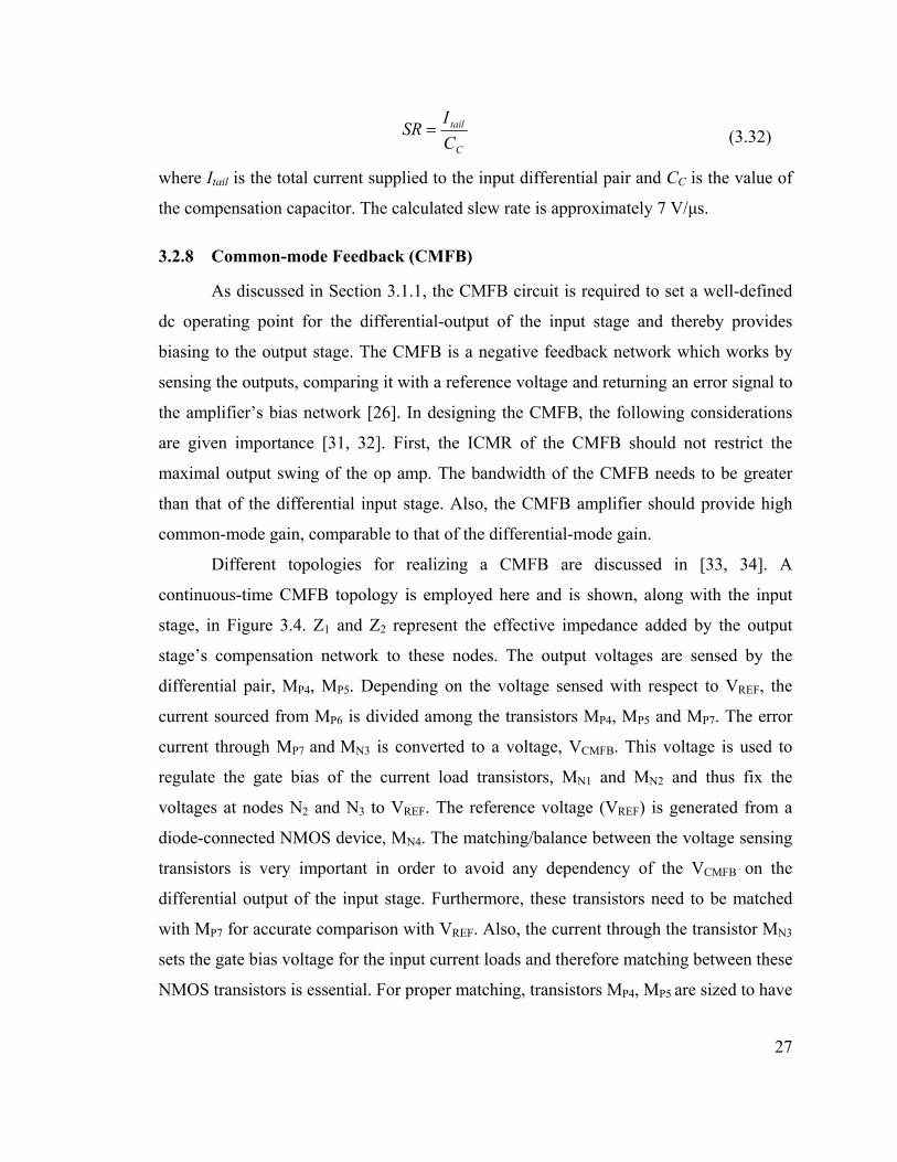
common-mode gain, comparable to that of the differential-mode gain.
Different topologies for realizing a CMFB are discussed in [33, 34]. A
continuous-time CMFB topology is employed here and is shown, along with the input
stage, in Figure 3.4. Z1 and Z2 represent the effective impedance added by the output
stage’s compensation network to these nodes. The output voltages are sensed by the
differential pair, MP4, MP5. Depending on the voltage sensed with respect to VREF, the
current sourced from MP6 is divided among the transistors MP4, MP5 and MP7. The error
current through MP7 and MN3 is converted to a voltage, VCMFB. This voltage is used to
regulate the gate bias of the current load transistors, MN1 and MN2 and thus fix the
voltages at nodes N2 and N3 to VREF. The reference voltage (VREF) is generated from a
diode-connected NMOS device, MN4. The matching/balance between the voltage sensing
transistors is very important in order to avoid any dependency of the VCMFB on the
differential output of the input stage. Furthermore, these transistors need to be matched
with MP7 for accurate comparison with VREF. Also, the current through the transistor MN3
sets the gate bias voltage for the input current loads and therefore matching between these
NMOS transistors is essential. For proper matching, transistors MP4, MP5 are sized to have
27
half the width as that of MP7. Also, these transistors have equal lengths and their body
contacts are connected to VDD. The current source, MP6 is mirrored to provide the same
current as in the input stage’s differential pair such that at dc quiescent operating point
the current through MP7 is equal to the sum of the currents through MP4 and MP5, and MN3
has the same current as the current loads. The mid-band loop gain from VN3,N2 to the
VN3,N2 node can be derived from small signal analysis as (Appendix A.3)
( )2,2,2,3,
4,, || MPoMNoMNm
MNm
MPmmidbandCMFB rrg
gg
A −≈ (3.33)
Substituting values for these parameters yields a voltage gain of about 106 V/V.
The dominant pole of the CMFB loop is at the output of the input stage which is
also equal to that of the differential input stage. By designing the gain of the CMFB loop
to be equal to that of the differential stage, the bandwidths can be made equal and thus
the speed of the CMFB would not restrict the operation of the input stage. The non-
dominant poles are expected to be at very high frequencies, so the CMFB acts like a
Figure 3.4 - Common-mode feedback circuit along with the input stage
28
single-pole system within the bandwidth and therefore stability of the op amp is not
compromised. The GBW of the loop can be expressed as [37]
( )
11,1,
3,
4,1,1,1,
)||(2
||
MMPoMNo
MNm
MPmMPoMNoMNm
DCMFB Crrgg
rrgpAGBW
π≈= (3.34)
where the loop gain is from equation (3.33). Substituting values in (3.34) gives the
expected bandwidth for the CMFB to be around 1 MHz. To verify this analysis, the
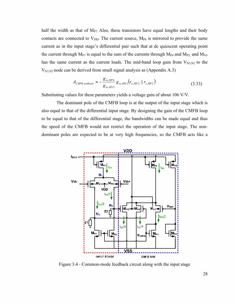
transmission loop frequency response of the CMFB was simulated and the Bode plot of
the magnitude and phase response is presented in Figure 3.5. The magnitude of the gain
is 40 dB which agrees well with the calculated result. Also the dominant pole occurs
around 5.8 KHz with a GBW of 900 KHz. The plots show the presence of a pole-zero
doublet before the unity-gain bandwidth of the op amp. The location of this doublet is
given in [43] as
⎟⎟⎠
⎞⎜⎜⎝
⎛+
−=
21
21
5,1
2MM
MM
MPm
CCCC
gp and
21
5,1
2
MM
MPm
CCg
z+
−=
(3.35)
where CM1 and CM2 are the Miller capacitances due to the compensation capacitors as in
(3.20). If the pole and zero are placed within a decade, they cancel out each other and
thus do not cause instability in the frequency-response or a large settling time in the
transient response. Also, the phase plot shows that the CMFB has a phase margin of 90°.
In order to determine the ICMR of the CMFB circuit alone, a ramp voltage was
applied as common-mode input to MP4 and MP5. The range of voltages for which all the
transistors in the CMFB (MP4-MP8, MN3-MN4) operate in saturation was obtained from
simulations as −1.2 to −0.6 V for complementary power supplies (±1.65 V). At dc, the
VREF is fixed as −0.915 V. With reasonable gain in the output stage of the op amp, for a
maximum output swing the required voltage swing at the output nodes of the input stage
is quite small. So the CMFB does not restrict the output swing. In order to verify the
performance, transient simulations were performed with common-mode and differential
signals applied to the op amp which is configured as a non-inverting, unity-gain buffer.
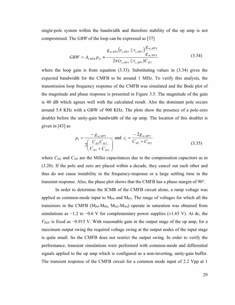
The transient response of the CMFB circuit for a common mode input of 2.2 Vpp at 1
29
-200
-150
-100
-50
0
50
100
150
200
1.00E+00 1.00E+02 1.00E+04 1.00E+06 1.00E+08 1.00E+10-200
-150
-100
-50
0
50
100
150
200
Vout Gain at N2Vout Gain at N3Vout Phase at N3Vout Phase at N2
Frequency (Hz)
Ope
n lo
opG
ain
(dB
)
Phas
e (
deg)P.M
Figure 3.5 - Simulated frequency response of CMFB circuit
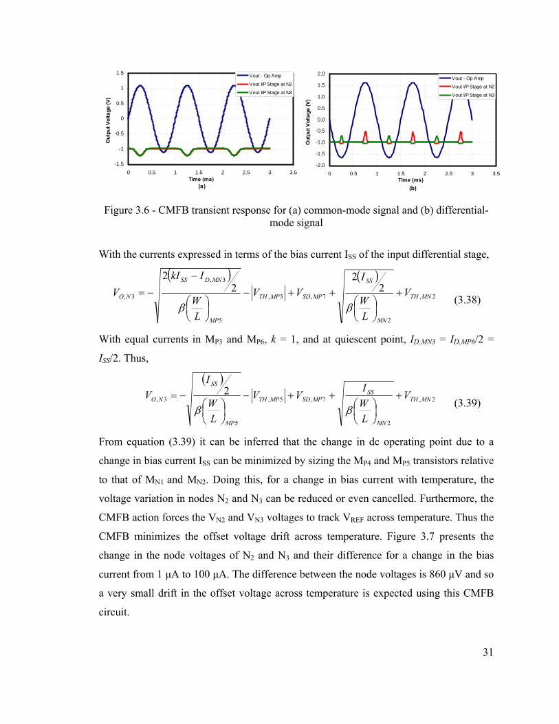
KHz to the op amp inputs is shown in Figure 3.6 (a). Input was restricted to 2.2 Vpp due
to the ICMR constraints of the op amp. Figure 3.6 (b) presents the case of maximum
output with differential inputs. Both plots show that the output swing of the op amp is not
limited by CMFB and the nodes N2 and N3 are regulated throughout the swing with all
the devices of CMFB circuit in saturation for the entire range of input voltages.
By fixing the dc quiescent output voltage of the input stage, the CMFB helps in
reducing the op amp’s offset and offset drift across temperature. For instance, consider
the change in bias current with the change in temperature. The mobility and therefore the
gm also vary, but the rate of change is different in the NMOS and PMOS devices. Hence
there would be a change in the random offset voltage given by (3.28). With the CMFB,
the output voltage at node N3 can be written as,
1,7,5,3, MNGSMPSDMPSGNO VVVV ++−= (3.36)
2,
2
2,7,5,
5
5,3,
22MNTH
MN
MNDMPSDMPTH
MP
MPDNO V
LWI
VV
LWI
V +⎟⎠⎞
⎜⎝⎛
++−⎟⎠⎞
⎜⎝⎛
−=ββ
(3.37)
30
-1.5
-1
-0.5
0
0.5
1
1.5
0 0.5 1 1.5 2 2.5 3 3.5
Vout - Op Amp
Vout I/P Stage at N2
Vout I/P Stage at N3
Time (ms)
Out
put V
olta
ge (V
)
(a)
-2.0
-1.5
-1.0
-0.5
0.0
0.5
1.0
1.5
2.0
0 0.5 1 1.5 2 2.5 3 3.5
Vout - Op Amp
Vout I/P Stage at N2
Vout I/P Stage at N3
Time (ms)
Out
put V
olta
ge (V
)
(b) Figure 3.6 - CMFB transient response for (a) common-mode signal and (b) differential-
mode signal
With the currents expressed in terms of the bias current ISS of the input differential stage,
( ) ( )2,
2
7,5,
5
3,
3,2
22
2
MNTH
MN
SS
MPSDMPTH
MP
MNDSS
NO V
LW
IVV
LW
IkIV +
⎟⎠⎞
⎜⎝⎛
++−⎟⎠⎞
⎜⎝⎛
−−=
ββ
(3.38)
With equal currents in MP3 and MP6, k = 1, and at quiescent point, ID,MN3 = ID,MP6/2 =
ISS/2. Thus,
( )2,
2
7,5,
5
3,2
MNTH
MN
SSMPSDMPTH
MP
SS
NO V
LWI
VV
LW
IV +
⎟⎠⎞
⎜⎝⎛
++−⎟⎠⎞
⎜⎝⎛
−=ββ
(3.39)
From equation (3.39) it can be inferred that the change in dc operating point due to a
change in bias current ISS can be minimized by sizing the MP4 and MP5 transistors relative
to that of MN1 and MN2. Doing this, for a change in bias current with temperature, the
voltage variation in nodes N2 and N3 can be reduced or even cancelled. Furthermore, the
CMFB action forces the VN2 and VN3 voltages to track VREF across temperature. Thus the
CMFB minimizes the offset voltage drift across temperature. Figure 3.7 presents the
change in the node voltages of N2 and N3 and their difference for a change in the bias
current from 1 μA to 100 μA. The difference between the node voltages is 860 μV and so
a very small drift in the offset voltage across temperature is expected using this CMFB
circuit.
31
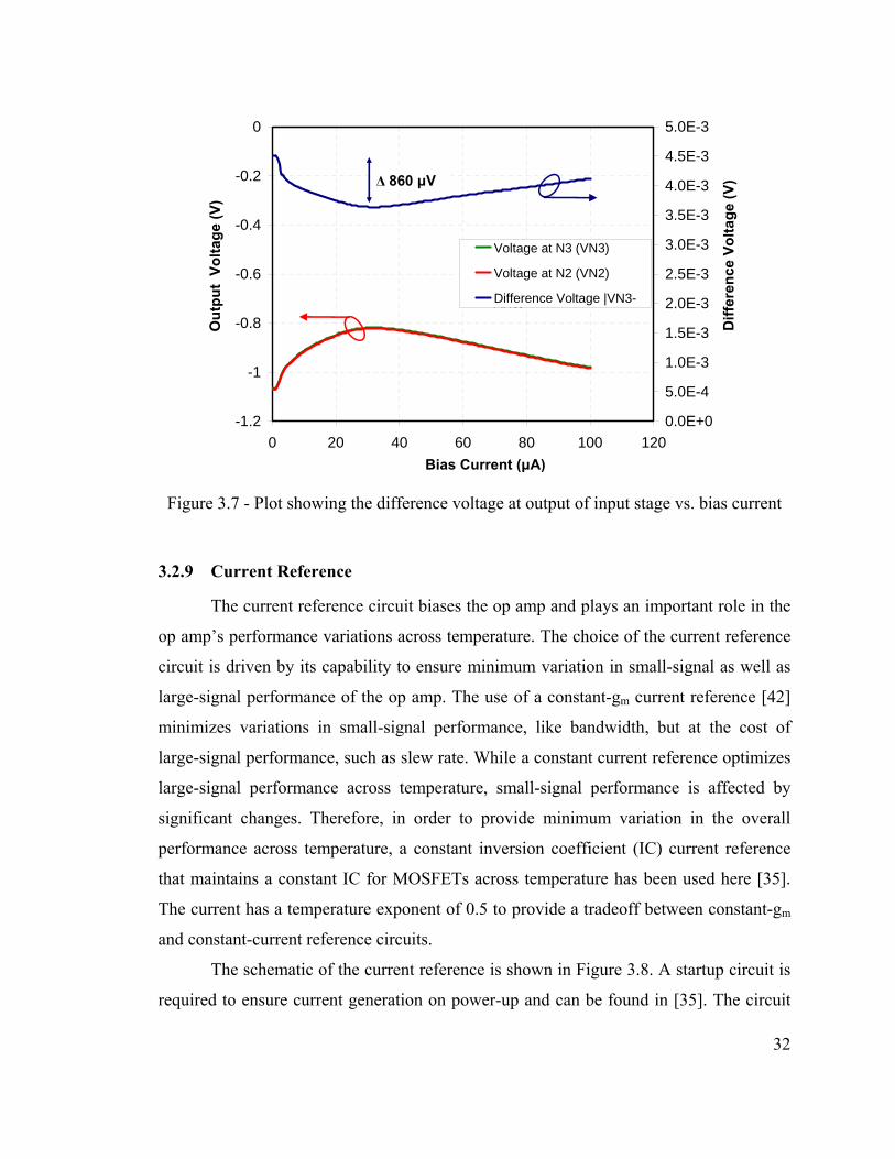
-1.2
-1
-0.8
-0.6
-0.4
-0.2
0
0 20 40 60 80 100 1200.0E+0
5.0E-4
1.0E-3
1.5E-3
2.0E-3
2.5E-3
3.0E-3
3.5E-3
4.0E-3
4.5E-3
5.0E-3
Voltage at N3 (VN3)
Voltage at N2 (VN2)
Difference Voltage |VN3-VN2|
Bias Current (μA)
Diff
eren
ce V
olta
ge (V
)
Out
put
Volta
ge (V
)
Δ 860 μV
Figure 3.7 - Plot showing the difference voltage at output of input stage vs. bias current
3.2.9 Current Reference
The current reference circuit biases the op amp and plays an important role in the
op amp’s performance variations across temperature. The choice of the current reference
circuit is driven by its capability to ensure minimum variation in small-signal as well as
large-signal performance of the op amp. The use of a constant-gm current reference [42]
minimizes variations in small-signal performance, like bandwidth, but at the cost of
large-signal performance, such as slew rate. While a constant current reference optimizes
large-signal performance across temperature, small-signal performance is affected by
significant changes. Therefore, in order to provide minimum variation in the overall
performance across temperature, a constant inversion coefficient (IC) current reference
that maintains a constant IC for MOSFETs across temperature has been used here [35].
The current has a temperature exponent of 0.5 to provide a tradeoff between constant-gm
and constant-current reference circuits.
The schematic of the current reference is shown in Figure 3.8. A startup circuit is
required to ensure current generation on power-up and can be found in [35]. The circuit
32
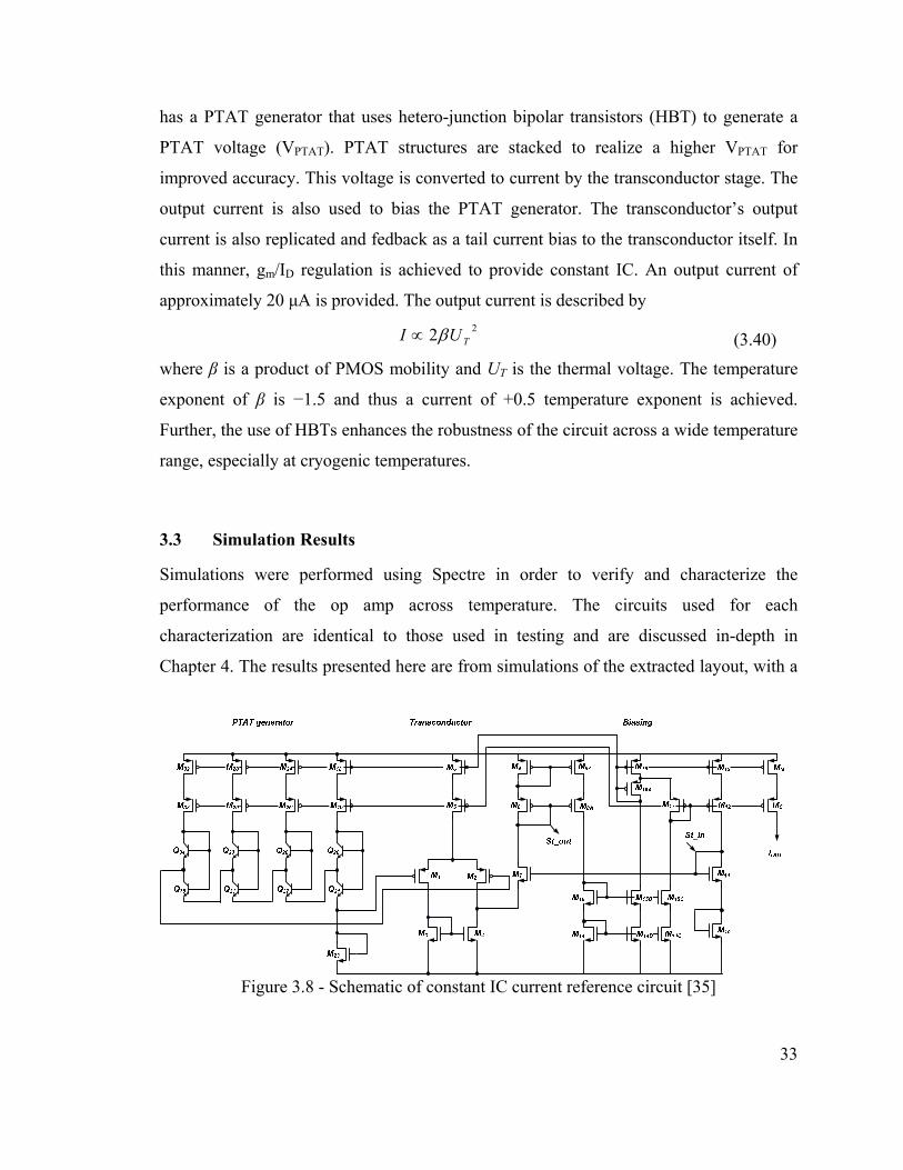
has a PTAT generator that uses hetero-junction bipolar transistors (HBT) to generate a
PTAT voltage (VPTAT). PTAT structures are stacked to realize a higher VPTAT for
improved accuracy. This voltage is converted to current by the transconductor stage. The
output current is also used to bias the PTAT generator. The transconductor’s output
current is also replicated and fedback as a tail current bias to the transconductor itself. In
this manner, gm/ID regulation is achieved to provide constant IC. An output current of
approximately 20 μA is provided. The output current is described by 22 TUI β∝ (3.40)
where β is a product of PMOS mobility and UT is the thermal voltage. The temperature
exponent of β is −1.5 and thus a current of +0.5 temperature exponent is achieved.
Further, the use of HBTs enhances the robustness of the circuit across a wide temperature
range, especially at cryogenic temperatures.
3.3 Simulation Results
Simulations were performed using Spectre in order to verify and characterize the
performance of the op amp across temperature. The circuits used for each
characterization are identical to those used in testing and are discussed in-depth in
Chapter 4. The results presented here are from simulations of the extracted layout, with a
Figure 3.8 - Schematic of constant IC current reference circuit [35]
33
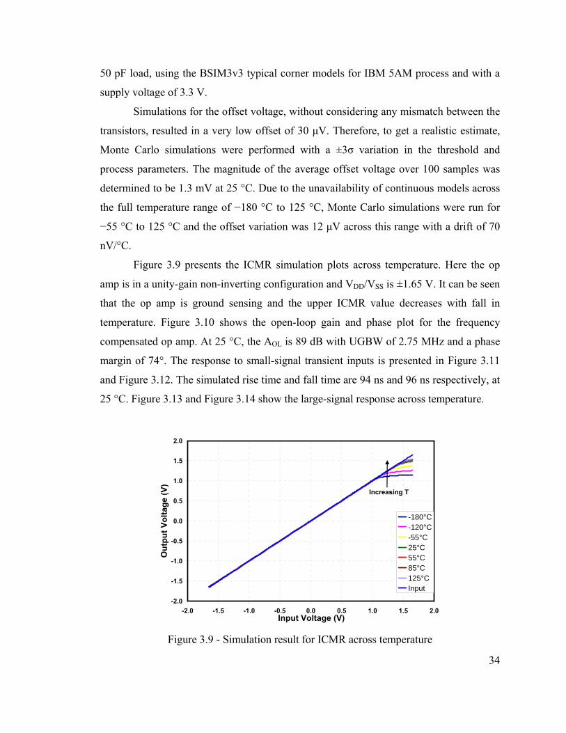
50 pF load, using the BSIM3v3 typical corner models for IBM 5AM process and with a
supply voltage of 3.3 V.
Simulations for the offset voltage, without considering any mismatch between the
transistors, resulted in a very low offset of 30 μV. Therefore, to get a realistic estimate,
Monte Carlo simulations were performed with a ±3σ variation in the threshold and
process parameters. The magnitude of the average offset voltage over 100 samples was
determined to be 1.3 mV at 25 °C. Due to the unavailability of continuous models across
the full temperature range of −180 °C to 125 °C, Monte Carlo simulations were run for
−55 °C to 125 °C and the offset variation was 12 μV across this range with a drift of 70
nV/°C.
Figure 3.9 presents the ICMR simulation plots across temperature. Here the op
amp is in a unity-gain non-inverting configuration and VDD/VSS is ±1.65 V. It can be seen
that the op amp is ground sensing and the upper ICMR value decreases with fall in
temperature. Figure 3.10 shows the open-loop gain and phase plot for the frequency
compensated op amp. At 25 °C, the AOL is 89 dB with UGBW of 2.75 MHz and a phase
margin of 74°. The response to small-signal transient inputs is presented in Figure 3.11
and Figure 3.12. The simulated rise time and fall time are 94 ns and 96 ns respectively, at
25 °C. Figure 3.13 and Figure 3.14 show the large-signal response across temperature.
-2.0
-1.5
-1.0
-0.5
0.0
0.5
1.0
1.5
2.0
-2.0 -1.5 -1.0 -0.5 0.0 0.5 1.0 1.5 2.0
-180°C-120°C-55°C25°C55°C85°C125°CInput
Input Voltage (V)
Out
put V
olta
ge (V
)
Increasing T
Figure 3.9 - Simulation result for ICMR across temperature
34
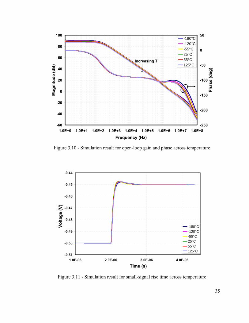
-60
-40
-20
0
20
40
60
80
100
1.0E+0 1.0E+1 1.0E+2 1.0E+3 1.0E+4 1.0E+5 1.0E+6 1.0E+7 1.0E+8
Frequency (Hz)
-250
-200
-150
-100
-50
0
50-180°C-120°C-55°C25°C55°C125°C
Mag
nitu
de (d
B)
Phas
e (d
eg)
Increasing T
Figure 3.10 - Simulation result for open-loop gain and phase across temperature
-0.51
-0.50
-0.49
-0.48
-0.47
-0.46
-0.45
-0.44
1.0E-06 2.0E-06 3.0E-06 4.0E-06
-180°C-120°C-55°C25°C55°C125°C
Volta
ge (V
)
Time (s)
Figure 3.11 - Simulation result for small-signal rise time across temperature
35
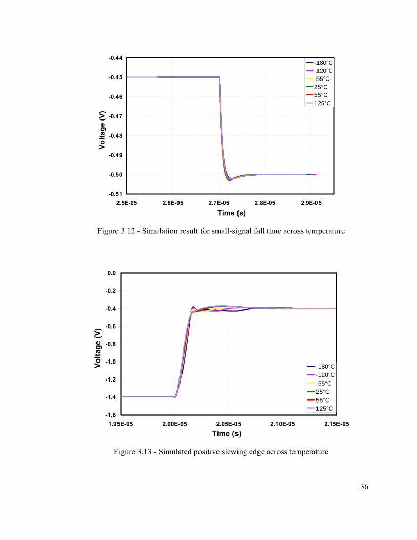
-0.51
-0.50
-0.49
-0.48
-0.47
-0.46
-0.45
-0.44
2.5E-05 2.6E-05 2.7E-05 2.8E-05 2.9E-05
-180°C-120°C-55°C25°C55°C125°C
Volta
ge (V
)
Time (s)
Figure 3.12 - Simulation result for small-signal fall time across temperature
-1.6
-1.4
-1.2
-1.0
-0.8
-0.6
-0.4
-0.2
0.0
1.95E-05 2.00E-05 2.05E-05 2.10E-05 2.15E-05
-180°C-120°C-55°C25°C55°C125°C
Time (s)
Volta
ge (V
)
Figure 3.13 - Simulated positive slewing edge across temperature
36
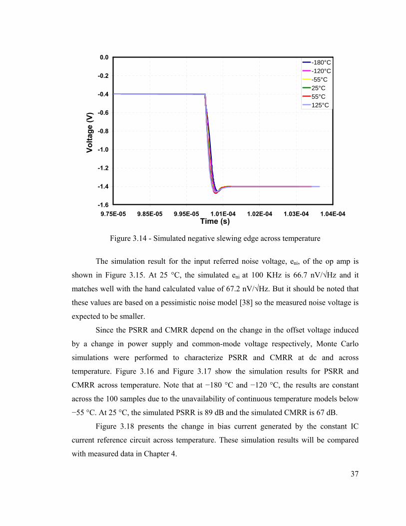
-1.6
-1.4
-1.2
-1.0
-0.8
-0.6
-0.4
-0.2
0.0
9.75E-05 9.85E-05 9.95E-05 1.01E-04 1.02E-04 1.03E-04 1.04E-04
-180°C-120°C-55°C25°C55°C125°C
Time (s)
Volta
ge (V
)
Figure 3.14 - Simulated negative slewing edge across temperature
The simulation result for the input referred noise voltage, eni, of the op amp is
shown in Figure 3.15. At 25 °C, the simulated eni at 100 KHz is 66.7 nV/√Hz and it
matches well with the hand calculated value of 67.2 nV/√Hz. But it should be noted that
these values are based on a pessimistic noise model [38] so the measured noise voltage is
expected to be smaller.
Since the PSRR and CMRR depend on the change in the offset voltage induced
by a change in power supply and common-mode voltage respectively, Monte Carlo
simulations were performed to characterize PSRR and CMRR at dc and across
temperature. Figure 3.16 and Figure 3.17 show the simulation results for PSRR and
CMRR across temperature. Note that at −180 °C and −120 °C, the results are constant
across the 100 samples due to the unavailability of continuous temperature models below
−55 °C. At 25 °C, the simulated PSRR is 89 dB and the simulated CMRR is 67 dB.
Figure 3.18 presents the change in bias current generated by the constant IC
current reference circuit across temperature. These simulation results will be compared
with measured data in Chapter 4.
37
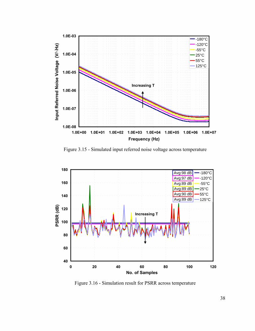
1.0E-08
1.0E-07
1.0E-06
1.0E-05
1.0E-04
1.0E-03
1.0E+00 1.0E+01 1.0E+02 1.0E+03 1.0E+04 1.0E+05 1.0E+06 1.0E+07Frequency (Hz)
-180°C-120°C-55°C25°C55°C125°C
Inpu
t Ref
erre
d N
oise
Vol
tage
(V/√H
z)
Increasing T
Figure 3.15 - Simulated input referred noise voltage across temperature
40
60
80
100
120
140
160
180
0 20 40 60 80 100 120No. of Samples
-180°C-120°C-55°C25°C55°C125°C
PSR
R (d
B)
Avg:98 dB
Avg:89 dB
Avg:89 dBAvg:89 dBAvg:97 dB
Avg:90 dB
Increasing T
Figure 3.16 - Simulation result for PSRR across temperature
38
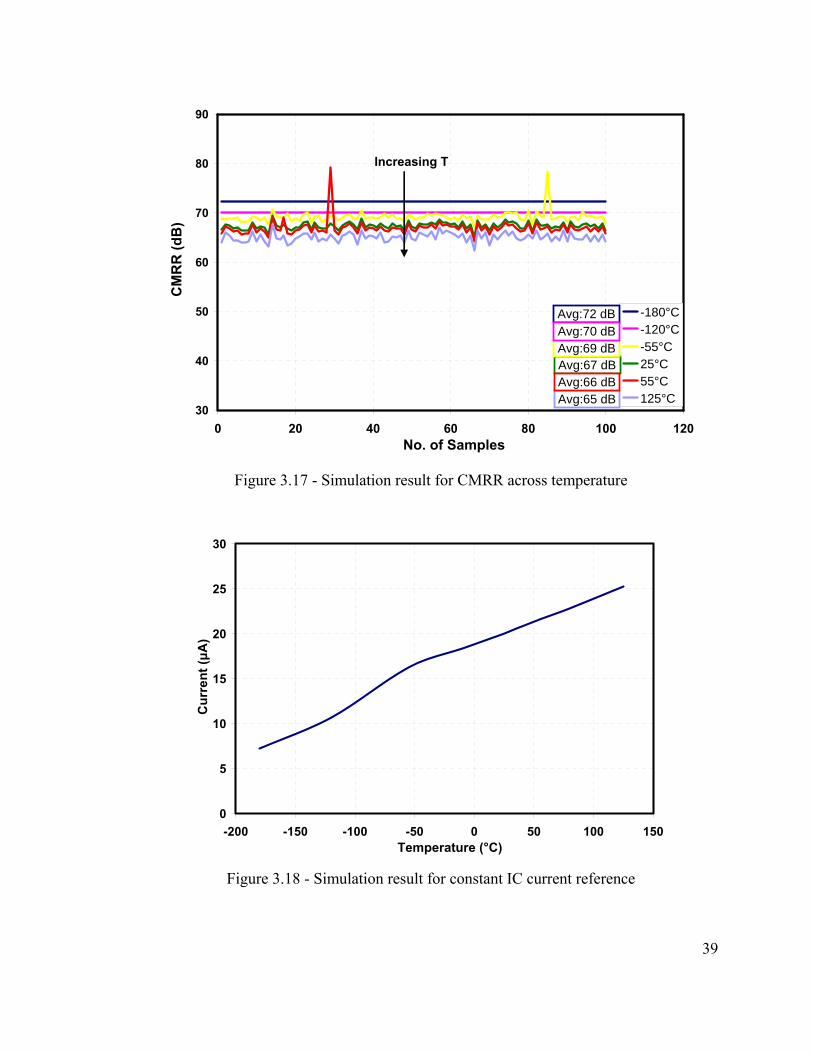
30
40
50
60
70
80
90
0 20 40 60 80 100 120
-180°C-120°C-55°C25°C55°C125°C
No. of Samples
CM
RR
(dB
)
Avg:72 dB
Avg:65 dB
Avg:67 dBAvg:69 dBAvg:70 dB
Avg:66 dB
Increasing T
Figure 3.17 - Simulation result for CMRR across temperature
0
5
10
15
20
25
30
-200 -150 -100 -50 0 50 100 150Temperature (°C)
Cur
rent
(μA
)
Figure 3.18 - Simulation result for constant IC current reference
39
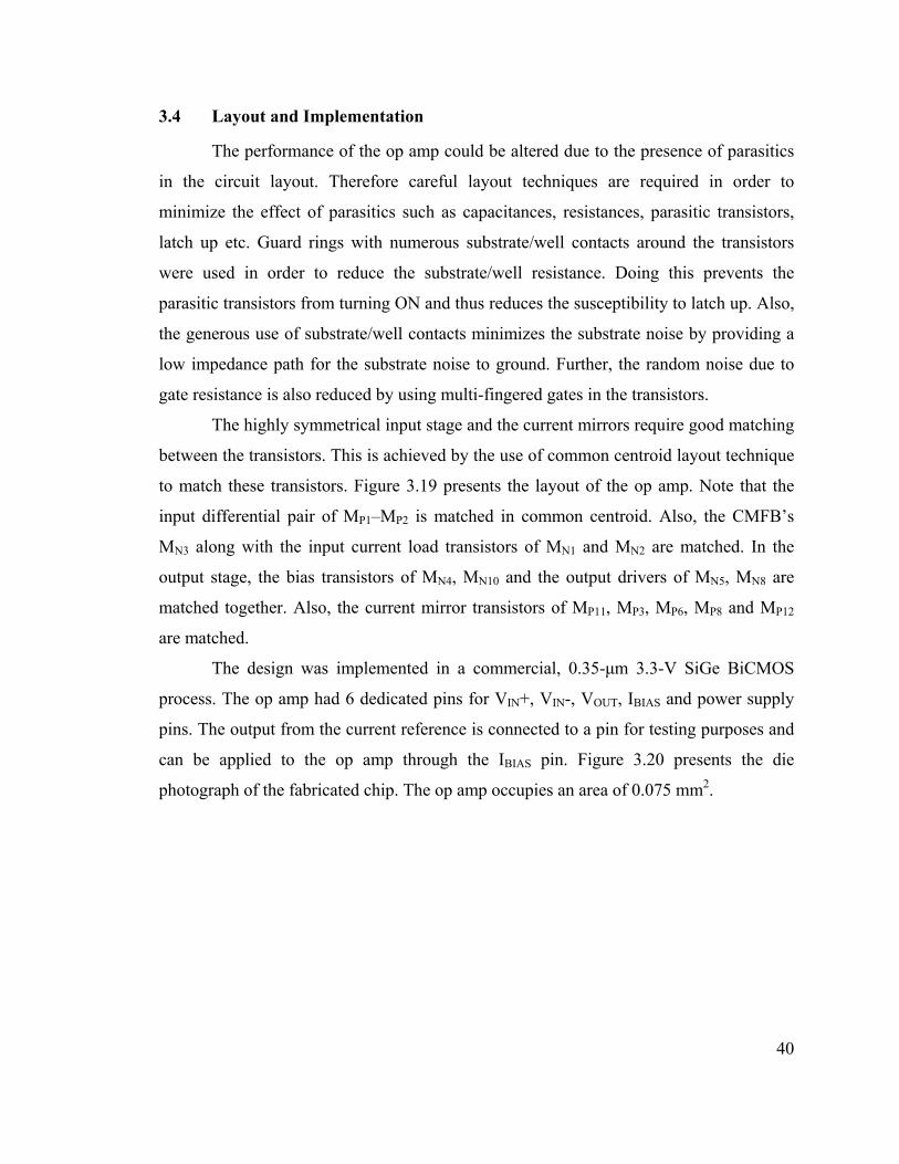
3.4 Layout and Implementation
The performance of the op amp could be altered due to the presence of parasitics
in the circuit layout. Therefore careful layout techniques are required in order to
minimize the effect of parasitics such as capacitances, resistances, parasitic transistors,
latch up etc. Guard rings with numerous substrate/well contacts around the transistors
were used in order to reduce the substrate/well resistance. Doing this prevents the
parasitic transistors from turning ON and thus reduces the susceptibility to latch up. Also,
the generous use of substrate/well contacts minimizes the substrate noise by providing a
low impedance path for the substrate noise to ground. Further, the random noise due to
gate resistance is also reduced by using multi-fingered gates in the transistors.
The highly symmetrical input stage and the current mirrors require good matching
between the transistors. This is achieved by the use of common centroid layout technique
to match these transistors. Figure 3.19 presents the layout of the op amp. Note that the
input differential pair of MP1–MP2 is matched in common centroid. Also, the CMFB’s
MN3 along with the input current load transistors of MN1 and MN2 are matched. In the
output stage, the bias transistors of MN4, MN10 and the output drivers of MN5, MN8 are
matched together. Also, the current mirror transistors of MP11, MP3, MP6, MP8 and MP12
are matched.
The design was implemented in a commercial, 0.35-μm 3.3-V SiGe BiCMOS
process. The op amp had 6 dedicated pins for VIN+, VIN-, VOUT, IBIAS and power supply
pins. The output from the current reference is connected to a pin for testing purposes and
can be applied to the op amp through the IBIAS pin. Figure 3.20 presents the die
photograph of the fabricated chip. The op amp occupies an area of 0.075 mm2.
40
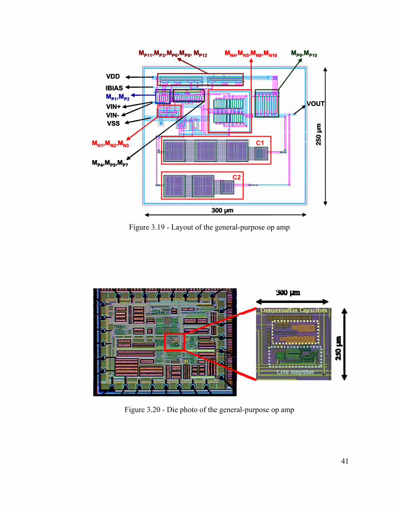
300 µm
250
µm
VDD
VSS
VIN+VIN-
VOUT
IBIAS
MN4,MN5,MN8,MN10
MN1,MN2,MN3
MP9,MP10MP11,MP3,MP6,MP8, MP12
C1
C2
MP4,MP5,MP7
MP1,MP2
300 µm
250
µm
VDD
VSS
VIN+VIN-
VOUT
IBIAS
MN4,MN5,MN8,MN10
MN1,MN2,MN3
MP9,MP10MP11,MP3,MP6,MP8, MP12
MP1,MP2
C1
C2
MP4,MP5,MP7
Figure 3.19 - Layout of the general-purpose op amp
Figure 3.20 - Die photo of the general-purpose op amp
41
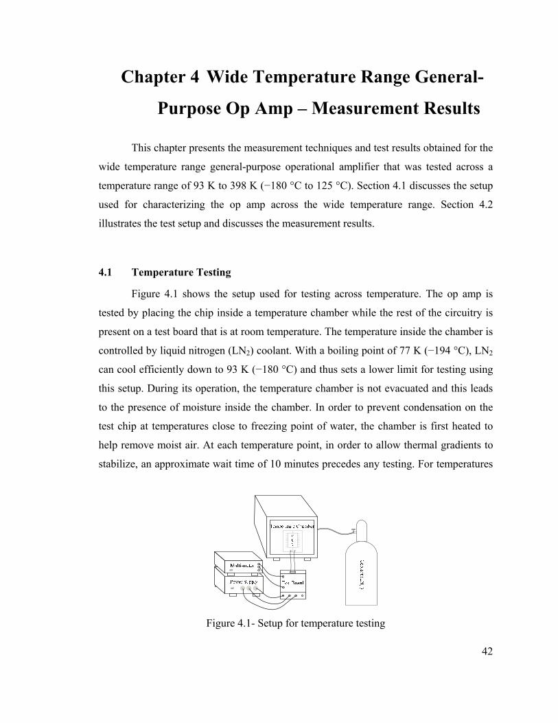
Chapter 4 Wide Temperature Range General-
Purpose Op Amp – Measurement Results
This chapter presents the measurement techniques and test results obtained for the
wide temperature range general-purpose operational amplifier that was tested across a
temperature range of 93 K to 398 K (−180 °C to 125 °C). Section 4.1 discusses the setup
used for characterizing the op amp across the wide temperature range. Section 4.2
illustrates the test setup and discusses the measurement results.
4.1 Temperature Testing
Figure 4.1 shows the setup used for testing across temperature. The op amp is
tested by placing the chip inside a temperature chamber while the rest of the circuitry is
present on a test board that is at room temperature. The temperature inside the chamber is
controlled by liquid nitrogen (LN2) coolant. With a boiling point of 77 K (−194 °C), LN2
can cool efficiently down to 93 K (−180 °C) and thus sets a lower limit for testing using
this setup. During its operation, the temperature chamber is not evacuated and this leads
to the presence of moisture inside the chamber. In order to prevent condensation on the
test chip at temperatures close to freezing point of water, the chamber is first heated to
help remove moist air. At each temperature point, in order to allow thermal gradients to
stabilize, an approximate wait time of 10 minutes precedes any testing. For temperatures
Figure 4.1- Setup for temperature testing
42
below 93 K, tests were performed in the cryogenic test system at the Georgia Institute of
Technology in Atlanta. Their system operates in vacuum and uses liquid Helium coolant
to achieve 4 K (−269 °C).
4.2 Test Setup
The test circuits necessary for characterizing the op amp were built on a printed
circuit board, shown in Appendix, Figure A.3, and used to test the op amp at room
temperature. Complementary supply voltages of ±1.65 V, from an Agilent E3631A, were
used to simplify testing by referencing the signals to a mid-supply voltage of ground.
Power supply bypassing capacitors were placed close to the supply pins of the op amp to
dampen any ac ripple and power supply noise. To filter out the power supply noise over a
wide bandwidth, an array of capacitors comprising of an electrolytic 100 μF, tantalum 1
μF and ceramic 0.1 μF were used. The op amp was biased by a 10 μA current sink which
was provided by the constant-IC current reference circuit, also fabricated in the same
chip. The output from the current reference of 20 μA is available at an output pin and this
current was fed to the op amp through another dedicated pin which supplies the required
bias current to the op amp by internally mirroring the 20 μA to 10 μA. If required, an
external source of current biasing can also be supplied through this pin. An effective load
capacitance of about 50 pF was connected to the op amp’s output for all test
configurations. An oscilloscope probe with a load of 15 pF, 10x attenuation, and 1 MΩ
impedance was used for all measurements (included in the 50 pF load estimate). A
sample of 5 chips was used for testing and the measurements results obtained show
consistent trend in the changes across the temperature range.
The setup to measure the systematic offset voltage has the op amp configured
with a non-inverting gain of 1,000 and a grounded positive input terminal as shown in
Figure 4.2. Using the Agilent 34401A multimeter, the offset VOUT was measured for
different chips. The average measured offset voltage for 5 chips at 25 °C is 1.62 mV and
this matches well with the Monte Carlo simulated value of 1.3 mV. The change in the
magnitude of VOS across temperature is plotted in Figure 4.3. The low offset can be
43
Figure 4.2 - Measurement setup for offset voltage
1.600
1.610
1.620
1.630
1.640
1.650
1.660
-200 -150 -100 -50 0 50 100 150
Mea
sure
d O
ffset
Vol
tage
(mV)
1.316
1.318
1.320
1.322
1.324
1.326
1.328
1.330
Sim
ulat
ed O
ffset
Vol
tage
(mV)
Chip 1Chip 2SimulatedTrend (Chip 2)
Temperature (°C)
Δ < 50 μV
Figure 4.3 - Measured VOS across temperature
44
attributed to the highly symmetrical input stage design, CMFB action, and good matching
provided by the common centroid layout technique. Thanks to the CMFB circuit, the
variation of the offset voltage across temperature is minimal and is measured to be less
than 50 μV and the drift is computed to be 85 nV/°C.
The ICMR is measured by configuring the op amp as a non-inverting unity gain
buffer as shown in Figure 4.4. A linear input ranging from VSS to VDD is applied to the op
amp and the output voltage is monitored. The range of input voltages for which the slope
of the output voltage is unity represents an estimate of the ICMR. At 25 °C, the measured
ICMR extends from 0 to 2.9 V which matches well with the simulated result of 0 to 3 V.
The lower range of ICMR extends to ground for the complete temperature range. Figure
4.5 shows the measured ICMR maximum voltage with variation in temperature. The
maximum range of ICMR decreases at LT due to the increase in VTH.
The open-loop gain of an op amp can be defined as
εVV
A OUTOL = (4.1)
where VOUT is the op amp’s output voltage, which is assumed to be zero when no input is
applied and Vε is the fedback error voltage, which is the input differential voltage applied
to the amplifier [36]. Due to the very high differential gain of the op amp, measuring the
gain using an open-loop configuration is very difficult, so the op amp is kept in a closed-
loop configuration.
Figure 4.4 - Measurement setup for ICMR
45
2.65
2.70
2.75
2.80
2.85
2.90
2.95
3.00
3.05
3.10
3.15
-200 -150 -100 -50 0 50 100 150
ICM
R (
V)
Chip 1Chip 2SimulatedTrend (Chip 1)
Temperature (°C) Figure 4.5 - Measured ICMR max across temperature
Figure 4.6 presents the setup used for the open-loop gain measurement where the
op amp is configured as a unity-gain amplifier. The signal is applied to the negative input
terminal while the positive input is grounded, thereby maintaining a fixed common-mode
voltage of ground, and therefore the finite open-loop gain can be differentiated from the
finite CMRR [36]. A large feedback resistor is chosen to prevent dc loading of the op
amp’s output. The probing of the error voltage Vε at the negative input terminal of the op
amp introduces capacitance at the node which, along with the large input resistance,
would form a low-frequency pole and thereby cause instability. Capacitor C1 fixes the
location of the input pole and capacitor CF adds a zero to improve the stability of the
system.
An SR770 network analyzer, which provides high resolution voltage
measurements, was used for the voltage measurements. The network analyzer has an
internal sine-wave synthesizer which is perfectly synchronized with the timing window
of the FFT analyzer. Using this sine wave as the op amp’s input prevents any spectral
leakage during the FFT analysis of the op amp’s output and thereby gives an accurate
measurement. A nominal input of 200 mV was applied for the measurements. The SR770
has a frequency limit of 100 kHz, so the op amp’s open-loop gain was characterized for
this range and unity gain bandwidth was derived by extrapolating the plot with a 20
dB/decade slope to cross the 0 dB line. Figure 4.7 shows the measured open-loop gain
46
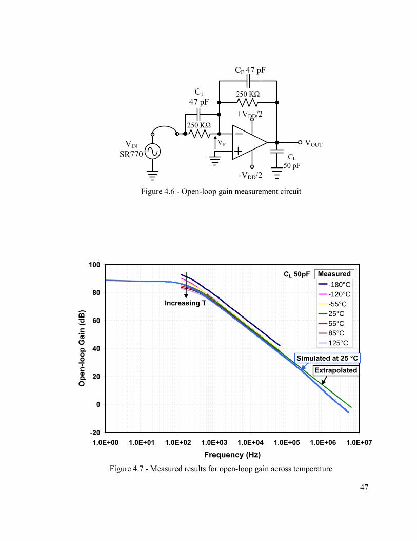
VINSR770
250 KΩ
CL50 pF
VOUT
+VDD/2
-VDD/2
CF 47 pF
Vε
250 KΩC147 pF
Figure 4.6 - Open-loop gain measurement circuit
-20
0
20
40
60
80
100
1.0E+00 1.0E+01 1.0E+02 1.0E+03 1.0E+04 1.0E+05 1.0E+06 1.0E+07
Frequency (Hz)
Ope
n-lo
op G
ain
(dB
)
-180°C-120°C-55°C25°C55°C85°C125°C
Measured
Simulated at 25 °CExtrapolated
Increasing T
CL 50pF
Figure 4.7 - Measured results for open-loop gain across temperature
47
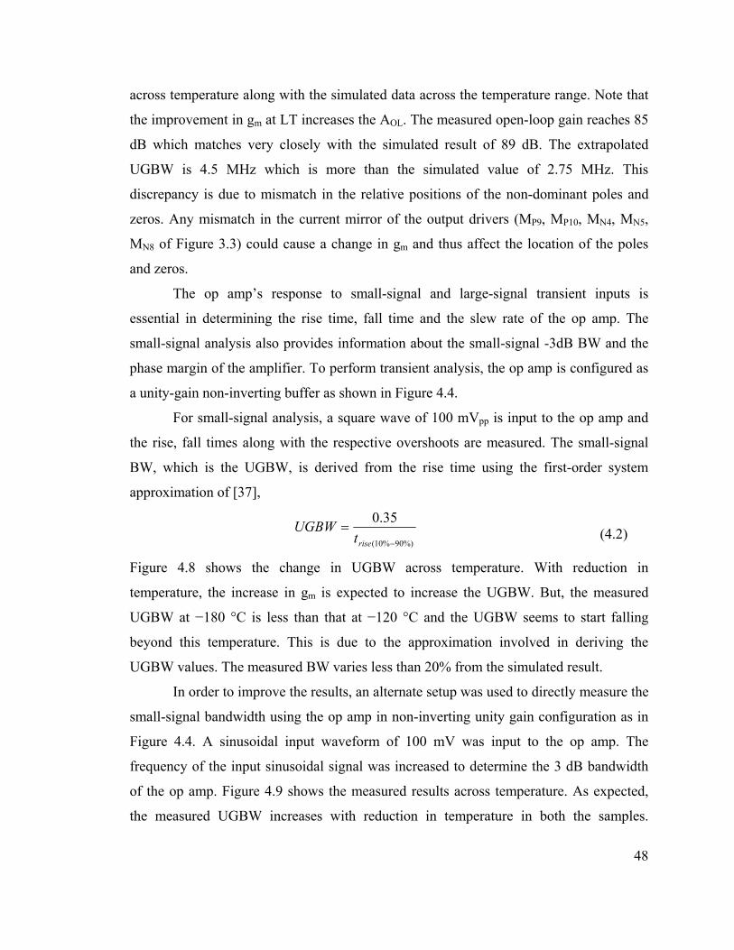
across temperature along with the simulated data across the temperature range. Note that
the improvement in gm at LT increases the AOL. The measured open-loop gain reaches 85
dB which matches very closely with the simulated result of 89 dB. The extrapolated
UGBW is 4.5 MHz which is more than the simulated value of 2.75 MHz. This
discrepancy is due to mismatch in the relative positions of the non-dominant poles and
zeros. Any mismatch in the current mirror of the output drivers (MP9, MP10, MN4, MN5,
MN8 of Figure 3.3) could cause a change in gm and thus affect the location of the poles
and zeros.
The op amp’s response to small-signal and large-signal transient inputs is
essential in determining the rise time, fall time and the slew rate of the op amp. The
small-signal analysis also provides information about the small-signal -3dB BW and the
phase margin of the amplifier. To perform transient analysis, the op amp is configured as
a unity-gain non-inverting buffer as shown in Figure 4.4.
For small-signal analysis, a square wave of 100 mVpp is input to the op amp and
the rise, fall times along with the respective overshoots are measured. The small-signal
BW, which is the UGBW, is derived from the rise time using the first-order system
approximation of [37],
%)90%10(
35.0
−
=riset
UGBW (4.2)
Figure 4.8 shows the change in UGBW across temperature. With reduction in
temperature, the increase in gm is expected to increase the UGBW. But, the measured
UGBW at −180 °C is less than that at −120 °C and the UGBW seems to start falling
beyond this temperature. This is due to the approximation involved in deriving the
UGBW values. The measured BW varies less than 20% from the simulated result.
In order to improve the results, an alternate setup was used to directly measure the
small-signal bandwidth using the op amp in non-inverting unity gain configuration as in
Figure 4.4. A sinusoidal input waveform of 100 mV was input to the op amp. The
frequency of the input sinusoidal signal was increased to determine the 3 dB bandwidth
of the op amp. Figure 4.9 shows the measured results across temperature. As expected,
the measured UGBW increases with reduction in temperature in both the samples.
48
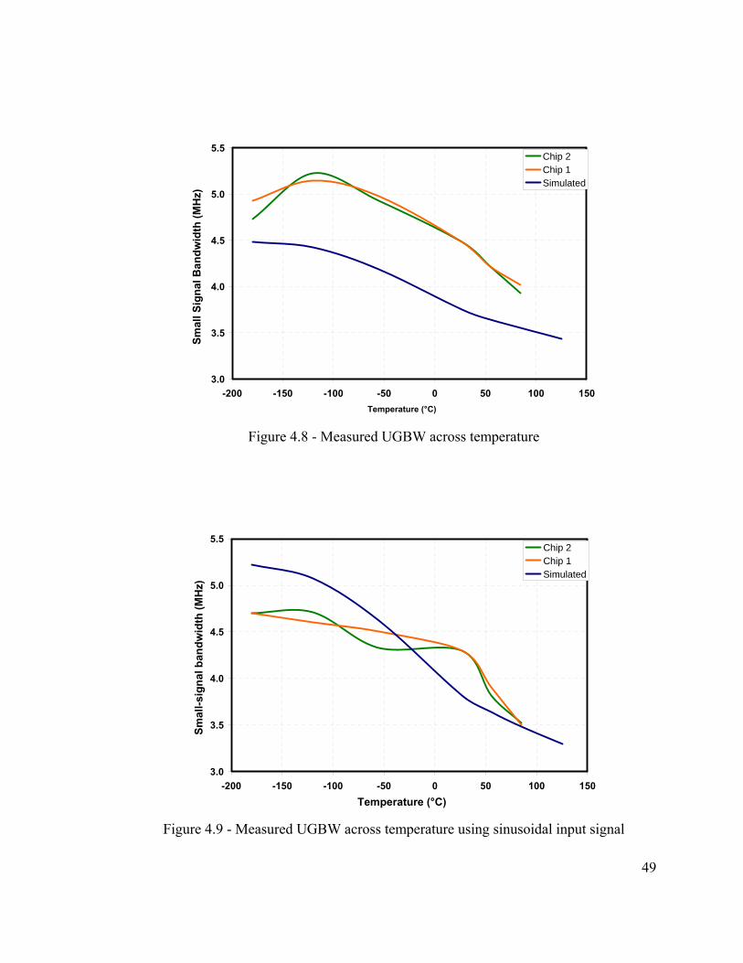
3.0
3.5
4.0
4.5
5.0
5.5
-200 -150 -100 -50 0 50 100 150
Chip 2Chip 1Simulated
Temperature (°C)
Smal
l Sig
nal B
andw
idth
(MH
z)
Figure 4.8 - Measured UGBW across temperature
3.0
3.5
4.0
4.5
5.0
5.5
-200 -150 -100 -50 0 50 100 150
Chip 2Chip 1Simulated
Temperature (°C)
Smal
l-sig
nal b
andw
idth
(MH
z)
Figure 4.9 - Measured UGBW across temperature using sinusoidal input signal
49
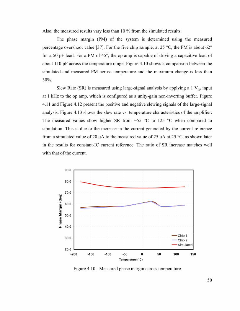
Also, the measured results vary less than 10 % from the simulated results.
The phase margin (PM) of the system is determined using the measured
percentage overshoot value [37]. For the five chip sample, at 25 °C, the PM is about 62°
for a 50 pF load. For a PM of 45°, the op amp is capable of driving a capacitive load of
about 110 pF across the temperature range. Figure 4.10 shows a comparison between the
simulated and measured PM across temperature and the maximum change is less than
30%.
Slew Rate (SR) is measured using large-signal analysis by applying a 1 Vpp input
at 1 kHz to the op amp, which is configured as a unity-gain non-inverting buffer. Figure
4.11 and Figure 4.12 present the positive and negative slewing signals of the large-signal
analysis. Figure 4.13 shows the slew rate vs. temperature characteristics of the amplifier.
The measured values show higher SR from −55 °C to 125 °C when compared to
simulation. This is due to the increase in the current generated by the current reference
from a simulated value of 20 μA to the measured value of 25 μA at 25 °C, as shown later
in the results for constant-IC current reference. The ratio of SR increase matches well
with that of the current.
20.0
30.0
40.0
50.0
60.0
70.0
80.0
90.0
-200 -150 -100 -50 0 50 100 150
Chip 1Chip 2Simulated
Temperature (°C)
Phas
e M
argi
n (d
eg)
Figure 4.10 - Measured phase margin across temperature
50
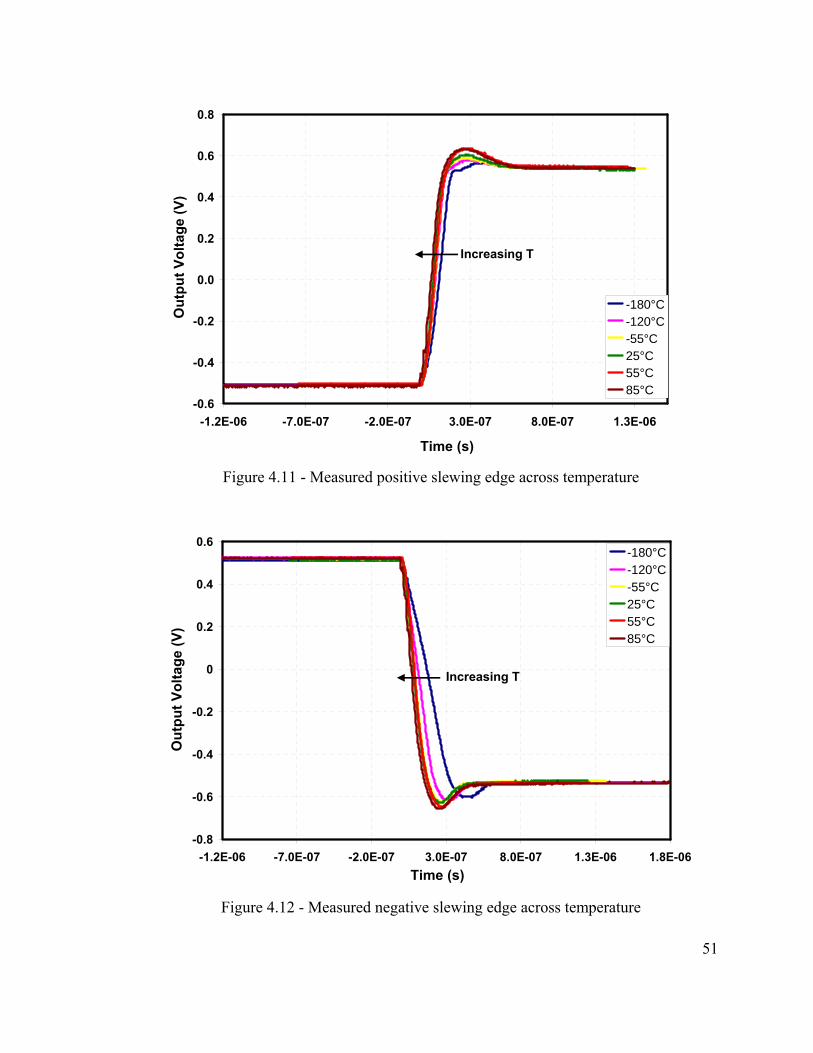
-0.6
-0.4
-0.2
0.0
0.2
0.4
0.6
0.8
-1.2E-06 -7.0E-07 -2.0E-07 3.0E-07 8.0E-07 1.3E-06
-180°C-120°C-55°C25°C55°C85°C
Time (s)
Out
put V
olta
ge (V
)
Increasing T
Figure 4.11 - Measured positive slewing edge across temperature
-0.8
-0.6
-0.4
-0.2
0
0.2
0.4
0.6
-1.2E-06 -7.0E-07 -2.0E-07 3.0E-07 8.0E-07 1.3E-06 1.8E-06
-180°C-120°C-55°C25°C55°C85°C
Out
put V
olta
ge (V
)
Time (s)
Increasing T
Figure 4.12 - Measured negative slewing edge across temperature
51
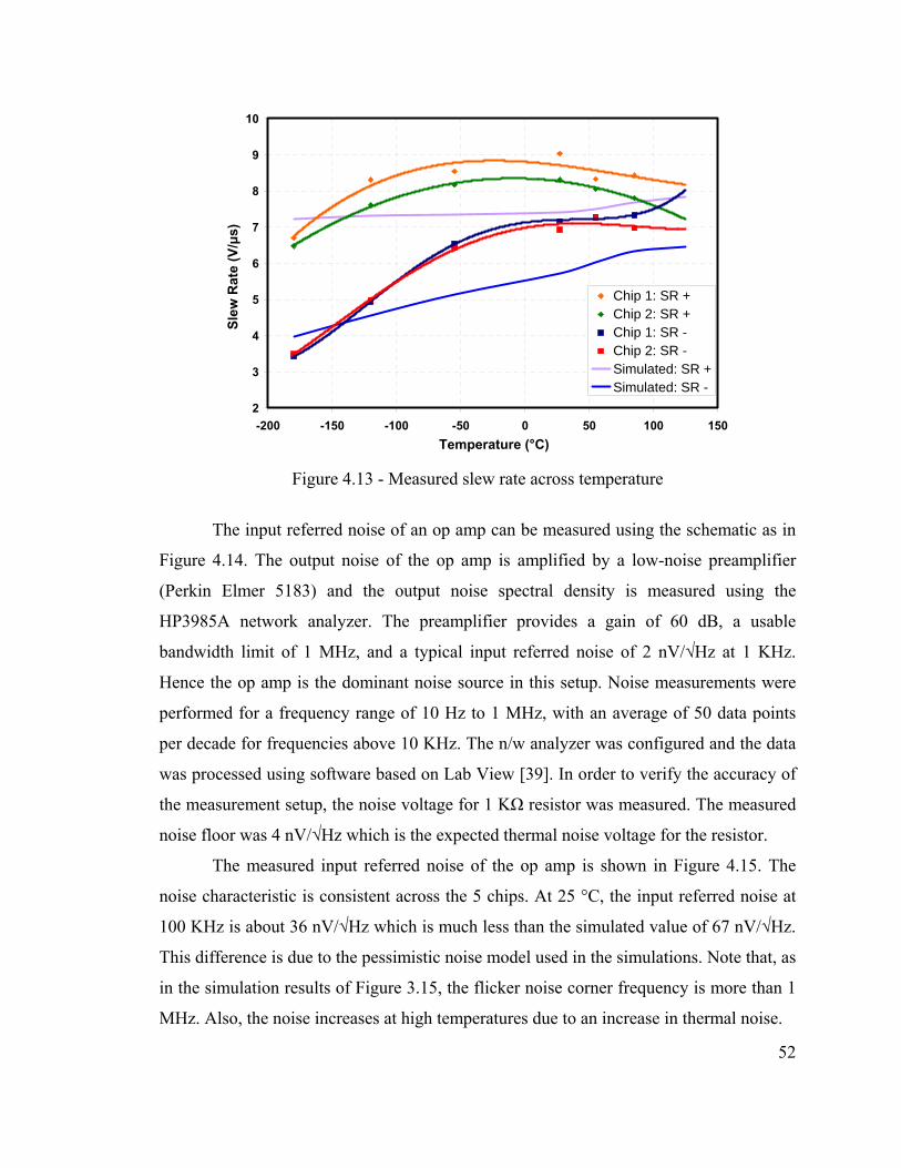
2
3
4
5
6
7
8
9
10
-200 -150 -100 -50 0 50 100 150
Chip 1: SR +Chip 2: SR +Chip 1: SR -Chip 2: SR -Simulated: SR +Simulated: SR -
Slew
Rat
e (V
/μs)
Temperature (°C) Figure 4.13 - Measured slew rate across temperature
The input referred noise of an op amp can be measured using the schematic as in
Figure 4.14. The output noise of the op amp is amplified by a low-noise preamplifier
(Perkin Elmer 5183) and the output noise spectral density is measured using the
HP3985A network analyzer. The preamplifier provides a gain of 60 dB, a usable
bandwidth limit of 1 MHz, and a typical input referred noise of 2 nV/√Hz at 1 KHz.
Hence the op amp is the dominant noise source in this setup. Noise measurements were
performed for a frequency range of 10 Hz to 1 MHz, with an average of 50 data points
per decade for frequencies above 10 KHz. The n/w analyzer was configured and the data
was processed using software based on Lab View [39]. In order to verify the accuracy of
the measurement setup, the noise voltage for 1 KΩ resistor was measured. The measured
noise floor was 4 nV/√Hz which is the expected thermal noise voltage for the resistor.
The measured input referred noise of the op amp is shown in Figure 4.15. The
noise characteristic is consistent across the 5 chips. At 25 °C, the input referred noise at
100 KHz is about 36 nV/√Hz which is much less than the simulated value of 67 nV/√Hz.
This difference is due to the pessimistic noise model used in the simulations. Note that, as
in the simulation results of Figure 3.15, the flicker noise corner frequency is more than 1
MHz. Also, the noise increases at high temperatures due to an increase in thermal noise.
52
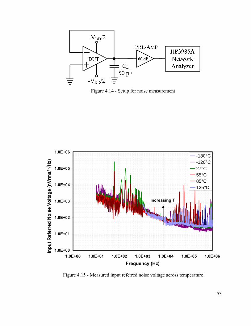
Figure 4.14 - Setup for noise measurement
1.0E+00
1.0E+01
1.0E+02
1.0E+03
1.0E+04
1.0E+05
1.0E+06
1.0E+00 1.0E+01 1.0E+02 1.0E+03 1.0E+04 1.0E+05 1.0E+06
Frequency (Hz)
-180°C-120°C27°C55°C85°C125°C
Inpu
t Ref
erre
d N
oise
Vol
tage
(nVr
ms/
√H
z)
Increasing T
Figure 4.15 - Measured input referred noise voltage across temperature
53
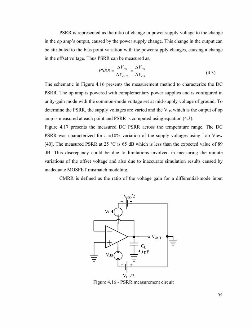
PSRR is represented as the ratio of change in power supply voltage to the change
in the op amp’s output, caused by the power supply change. This change in the output can
be attributed to the bias point variation with the power supply changes, causing a change
in the offset voltage. Thus PSRR can be measured as,
OS
PS
OUT
PS
VV
VV
PSRRΔΔ
=ΔΔ
= (4.3)
The schematic in Figure 4.16 presents the measurement method to characterize the DC
PSRR. The op amp is powered with complementary power supplies and is configured in
unity-gain mode with the common-mode voltage set at mid-supply voltage of ground. To
determine the PSRR, the supply voltages are varied and the VOS which is the output of op
amp is measured at each point and PSRR is computed using equation (4.3).
Figure 4.17 presents the measured DC PSRR across the temperature range. The DC
PSRR was characterized for a ±10% variation of the supply voltages using Lab View
[40]. The measured PSRR at 25 °C is 65 dB which is less than the expected value of 89
dB. This discrepancy could be due to limitations involved in measuring the minute
variations of the offset voltage and also due to inaccurate simulation results caused by
inadequate MOSFET mismatch modeling.
CMRR is defined as the ratio of the voltage gain for a differential-mode input
Figure 4.16 - PSRR measurement circuit
54
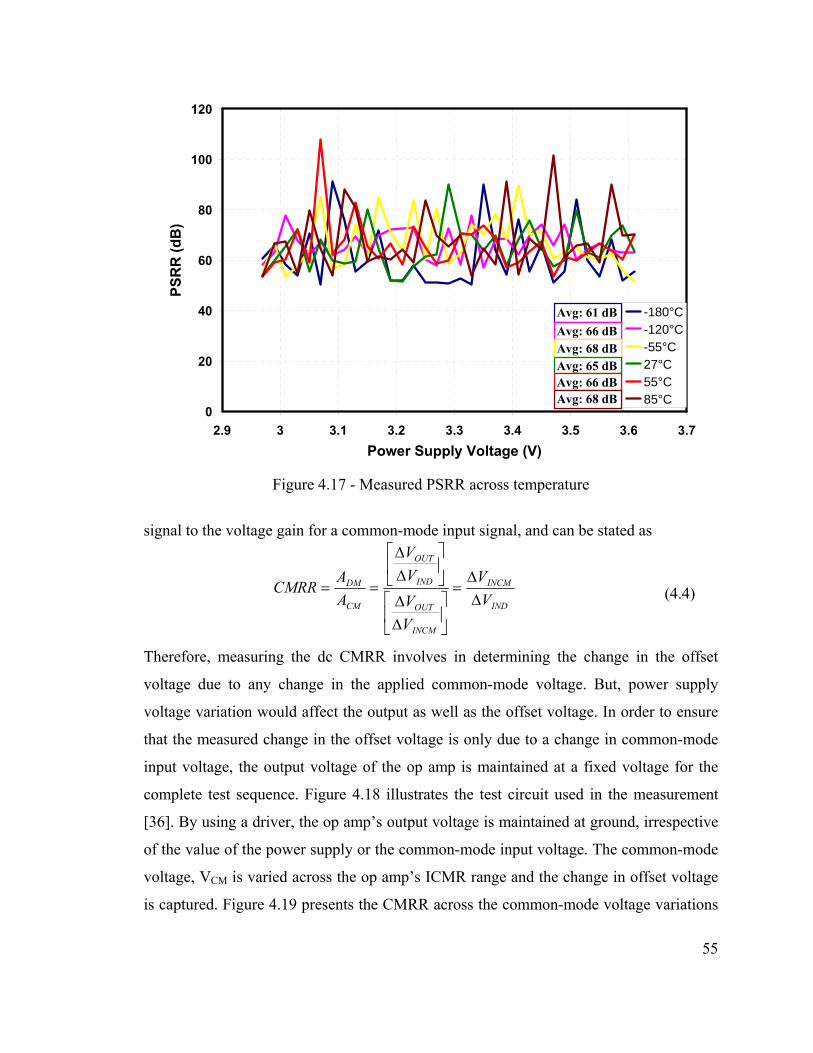
0
20
40
60
80
100
120
2.9 3 3.1 3.2 3.3 3.4 3.5 3.6 3.7Power Supply Voltage (V)
PSR
R (d
B)
-180°C-120°C-55°C27°C55°C85°C
Avg: 61 dBAvg: 66 dBAvg: 68 dBAvg: 65 dBAvg: 66 dBAvg: 68 dB
Figure 4.17 - Measured PSRR across temperature
signal to the voltage gain for a common-mode input signal, and can be stated as
IND
INCM
INCM
OUT
IND
OUT
CM
DM
VV
VVVV
AA
CMRRΔΔ
=
⎥⎦
⎤⎢⎣
⎡ΔΔ
⎥⎦
⎤⎢⎣
⎡ΔΔ
== (4.4)
Therefore, measuring the dc CMRR involves in determining the change in the offset
voltage due to any change in the applied common-mode voltage. But, power supply
voltage variation would affect the output as well as the offset voltage. In order to ensure
that the measured change in the offset voltage is only due to a change in common-mode
input voltage, the output voltage of the op amp is maintained at a fixed voltage for the
complete test sequence. Figure 4.18 illustrates the test circuit used in the measurement
[36]. By using a driver, the op amp’s output voltage is maintained at ground, irrespective
of the value of the power supply or the common-mode input voltage. The common-mode
voltage, VCM is varied across the op amp’s ICMR range and the change in offset voltage
is captured. Figure 4.19 presents the CMRR across the common-mode voltage variations
55
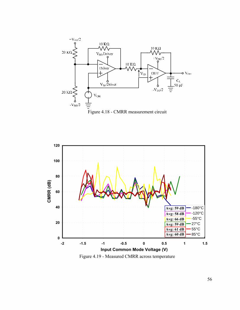
Figure 4.18 - CMRR measurement circuit
0
20
40
60
80
100
120
-2 -1.5 -1 -0.5 0 0.5 1 1.5
-180°C-120°C-55°C27°C55°C85°C
Avg: 59 dBAvg: 58 dBAvg: 66 dBAvg: 59 dBAvg: 61 dBAvg: 60 dB
Input Common Mode Voltage (V)
CM
RR
(dB
)
Figure 4.19 - Measured CMRR across temperature
56
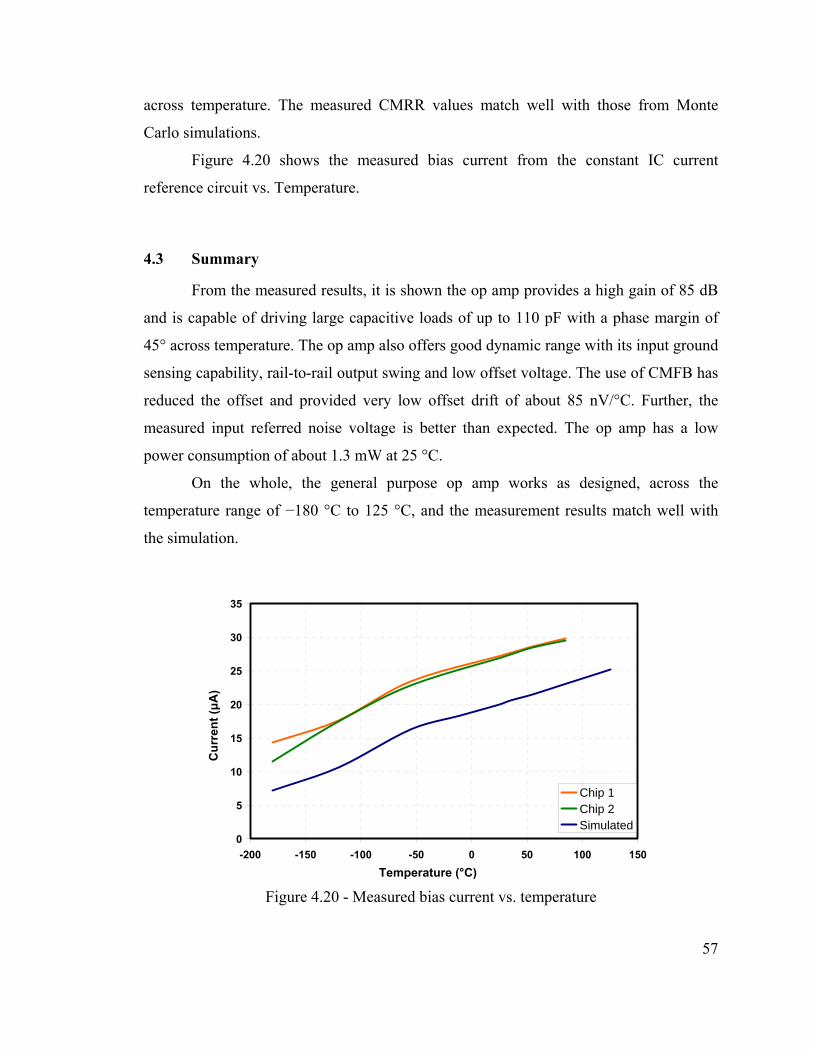
across temperature. The measured CMRR values match well with those from Monte
Carlo simulations.
Figure 4.20 shows the measured bias current from the constant IC current
reference circuit vs. Temperature.
4.3 Summary
From the measured results, it is shown the op amp provides a high gain of 85 dB
and is capable of driving large capacitive loads of up to 110 pF with a phase margin of
45° across temperature. The op amp also offers good dynamic range with its input ground
sensing capability, rail-to-rail output swing and low offset voltage. The use of CMFB has
reduced the offset and provided very low offset drift of about 85 nV/°C. Further, the
measured input referred noise voltage is better than expected. The op amp has a low
power consumption of about 1.3 mW at 25 °C.
On the whole, the general purpose op amp works as designed, across the
temperature range of −180 °C to 125 °C, and the measurement results match well with
the simulation.
0
5
10
15
20
25
30
35
-200 -150 -100 -50 0 50 100 150
Chip 1Chip 2Simulated
Cur
rent
(μA
)
Temperature (°C)
Figure 4.20 - Measured bias current vs. temperature
57
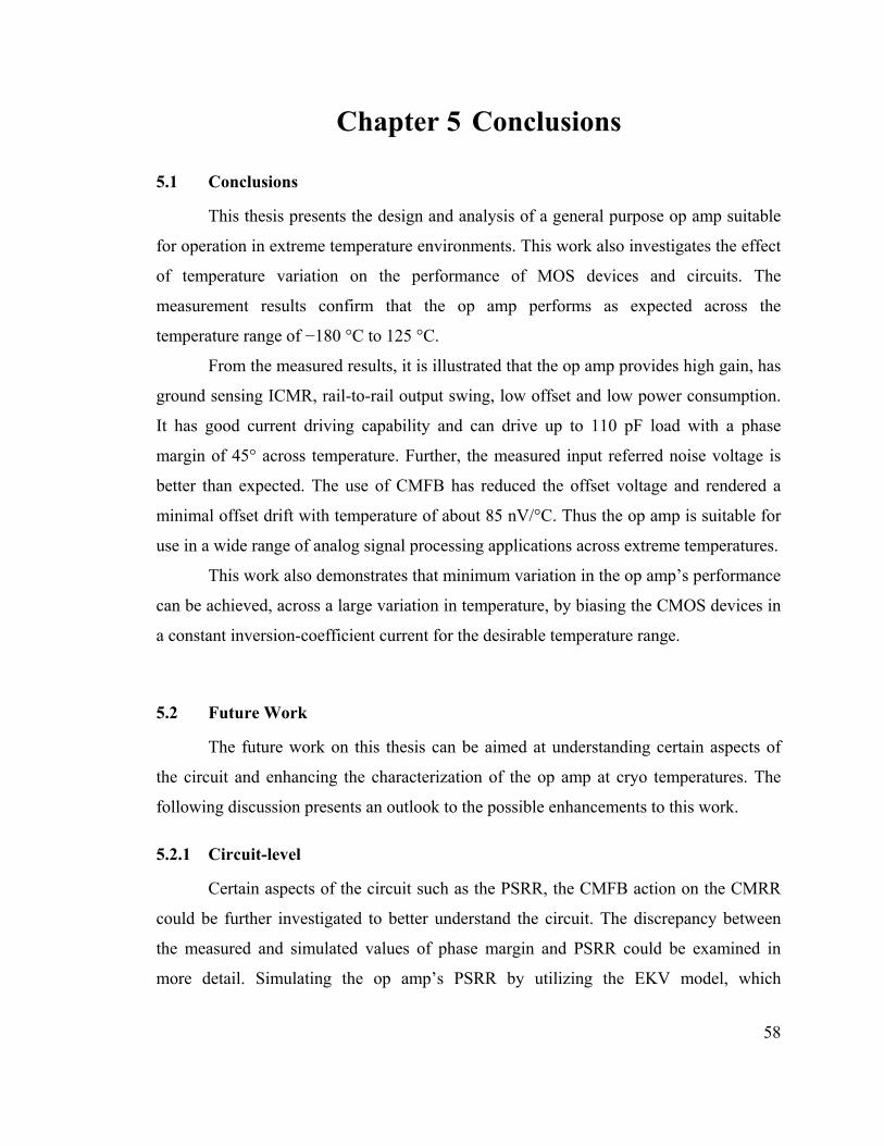
Chapter 5 Conclusions
5.1 Conclusions
This thesis presents the design and analysis of a general purpose op amp suitable
for operation in extreme temperature environments. This work also investigates the effect
of temperature variation on the performance of MOS devices and circuits. The
measurement results confirm that the op amp performs as expected across the
temperature range of −180 °C to 125 °C.
From the measured results, it is illustrated that the op amp provides high gain, has
ground sensing ICMR, rail-to-rail output swing, low offset and low power consumption.
It has good current driving capability and can drive up to 110 pF load with a phase
margin of 45° across temperature. Further, the measured input referred noise voltage is
better than expected. The use of CMFB has reduced the offset voltage and rendered a
minimal offset drift with temperature of about 85 nV/°C. Thus the op amp is suitable for
use in a wide range of analog signal processing applications across extreme temperatures.
This work also demonstrates that minimum variation in the op amp’s performance
can be achieved, across a large variation in temperature, by biasing the CMOS devices in
a constant inversion-coefficient current for the desirable temperature range.
5.2 Future Work
The future work on this thesis can be aimed at understanding certain aspects of
the circuit and enhancing the characterization of the op amp at cryo temperatures. The
following discussion presents an outlook to the possible enhancements to this work.
5.2.1 Circuit-level
Certain aspects of the circuit such as the PSRR, the CMFB action on the CMRR
could be further investigated to better understand the circuit. The discrepancy between
the measured and simulated values of phase margin and PSRR could be examined in
more detail. Simulating the op amp’s PSRR by utilizing the EKV model, which
58
incorporates an accurate MOSFET mismatch model, might help in improving the
accuracy of PSRR simulations. A study of EKV and the BSIM models could also give
more insight into the circuit operation. A revised test setup could be used to characterize
the PSRR and CMRR as a function of frequency.
5.2.2 System-level
This work is intended for use in space applications, specifically in lunar missions
where the temperature inside lunar craters can go down to −230 °C. Therefore it is
essential to investigate the op amp’s operation across wide temperature swings ranging
from −230 °C to 120 °C and as well as in radiation intense environments. With this focus,
the op amp was tested at −230 °C in the cryogenic test system at the Georgia Institute of
Technology in Atlanta. The test results proved that the circuit is fully functional at −230
°C. Although the op amp operates satisfactorily in the desirable temperature range and
the degradation effects due to the extreme temperature operation were not noticeable,
further verification is needed before assuring the long-term operability of the circuit. The
accumulative effects of temperature variation on the lifetime of the devices due to
degradation mechanisms such as hot carrier effects, oxide breakdown and carrier freeze
out have to be evaluated especially for operations below −180 °C.
Additionally, to study the impact of radiation exposure on the performance of the
op amp, the circuit was irradiated with 63 MeV protons at 25 °C at the Crocker Nuclear
Laboratory at UC Davis. The samples were subjected to 3 different dosage levels of 30,
100 and 300 Krads. Preliminary measurement results at 25 °C show minimal variations in
the op amp performance when compared to the pre-radiation results. Device level
characterization could be done to study the degradation in mobility, gm, and reduction in
threshold voltage due to radiation. Temperature testing is yet to be performed on these
irradiated samples and a thorough analysis of the results is necessary to determine the
radiation tolerance of the circuit.
Also, in order to suit the application, modifications could be made to the op amp
circuit to improve its performance. For instance, a buffer stage could be added at the
output to improve the drive capability of the op amp.
59

REFERENCES
60
[1] Bruce Carter and Thomas R.Brown, “Handbook of Operational Amplifer Applications”, Application Report, Texas Instruments, Oct. 2001.
[2] John D. Cressler, “On the Potentials of SiGe HBTs for Extreme Environment
Electronics” Proceedings of the IEEE, Vol. 93, No. 9, pp. 1559-1582, Sep. 2005. [3] The NASA, Mars Exploration Rover Mission, http://marsrovers.nasa.gov/mission/ [4] John D. Cressler and SiGe Code TTeam, “SiGe Code T Project: Month 4
Review” Oct. 2005. [5] Gray, Hurst, Lewis, Meyer, “Analysis and Design of Analog Integrated Circuits”,
Wiley, New York, 2001. [6] Jim Karki, “Understanding Operational Amplifier Specifications”, Digital Signal
Processing Solutions, Apr. 1998. [7] E. J. Kennedy, “Operational Amplifier Circuits, Theory and Applications”, Holt,
Rinehart and Winston, Inc, New York, 1988. [8] F. H. Gaensslen, D. D. Meyer, “Liquid Nitrogen CMOS for Computer
Applications”, IEEE International conference on Computer Design, pp. 4-8, Oct. 1991.
[9] G. Ghibaudo, F. Balestra, “Low Temperature Characterization of Silicon CMOS
Devices”, IEEE International Conference on Microelectronics, Vol. 2, pp. 613-622, Sep. 1995.
[10] William F. Clark et al, “Low Temperature CMOS – A Brief Review”, IEEE
Transactions on Components, Hybrids, and Manufacturing Technology, Vol. 15, No. 3, pp. 397- 404, Jun.1992.
[11] F. H. Gaensslen et al, “Very small MOSFETs for Low Temperature Operation”,
IEEE Transaction on Electron Devices, Vol. ED-24, No. 3, pp. 218- 229, Mar. 1997.
[12] Raymond Wang et al, “Threshold Voltage Variations with Temperature in MOS
Transistors”, IEEE Transactions on Electron Devices, Vol. 18, Issue 6, pp. 386-388, Jun. 1971.
[13] Stephen C. Terry et al, “Development of Robust Analog Electronics at the
University of Tennessee for NASA/JPL Extreme Environment Applications”, Proceedings of the 15th Biennial University/Government/Industry Microelectronics Symposium, pp. 124-127, Jun. 2003.
61
[14] Robert M. Fox, Richard C. Jaeger, “MOSFET Behavior and Circuit Considerations for Analog Applications at 77K”, IEEE Transactions on Electron Devices, Vol. ED-34, No. 1, pp. 114-123, Jan. 1997.
[15] S. T. Gunaseelan et al, “Low Temperature Performance of Operational Amplifiers
for Space Applications”, IEEE CCECE, Vol. 1, pp. 231-234, May 2003. [16] Neil H. E. Weste, David Harris, “CMOS VLSI Design, A Circuits and Systems
Perspective”, Pearson Education, 2005. [17] C. R. Viswanathan, “Low Temperature Characterization of CMOS Devices”,
International Symposium on VLSI Technology, Systems and Applications, pp. 207-212, May 1989.
[18] F. S. Shoucair, “Potential and problems of high-temperature electronics and
CMOS integrated circuits (25-250 °C) – an overview”, Microelectronics Journal, Vol. 22, No.2, pp.39-54, 1991.
[19] F. S. Shoucair, “Design considerations in High Temperature Analog CMOS
Integrated Circuits”, IEEE Transactions on Components, Hybrids, and Manufacturing Technology, Vol. CHMT-9, No.3, pp.242-251, Sep. 1986.
[20] J.Bergmann and A.ten Have, “High Temperature Operational Amplifier with low
offset voltage”, IEEE Proceedings of URSI International Symposium on Signals,Systems and Electronics, pp.451-454, Oct. 1995.
[21] Ashraf A.Osman et al, “Investigation of High Temperature Effects on MOSFET
Transconductance (gm)”, Fourth Intl. High Temperature Electronics Conference, pp.301-304, Jun. 1998.
[22] Philip Brusius, “Some Reliability Aspects of High Temperature ICs”, Fourth
International High Temperature Electronics Conference, pp.151-154, Jun. 1998. [23] Takahiro Aoki, “A discussion on the Temperature Dependence of Latch-Up
Trigger Current in CMOS/BiCMOS Structures”, IEEE Transactions on Electron Devices, Vol. 40, No. 11, pp.2023-2028, Nov. 1993.
[24] B. J. Blalock, “A 1-Volt CMOS Wide Dynamic Range Operational Amplifier”,
Ph.D Dissertation, School of ECE, Georgia Institute of Technology, Atlanta, GA, 1996.
[25] P. E. Allen, D. R. Holberg, “CMOS Analog Circuit Design”, Oxford University
Press, New York, 2002. [26] B. Razavi, “Design of Analog CMOS Integrated Circuits”, Mc Graw-Hill, 2001.
62
[27] D.A. Johns, Ken Martin, “Analog Integrated Circuit Design”, John Wiley & Sons, Inc., 1996.
[28] Joseph N. Babanezhad, “A Rail-to-Rail CMOS Op Amp”, IEEE JSSC, Vol. 23,
No. 6, pp. 1414 -1417, Dec.1988. [29] William C. Black, Jr. et al, “A High Performance Low Power CMOS Channel
Filter”, IEEE JSSC, Vol. SC-15, No. 6, pp. 929 - 938, Dec. 1980. [30] M. J. M. Pelgrom et al, “Matching properties of MOS Transistors”, IEEE JSSC,
Vol. 24, No. 5, pp. 1433-1440, Oct. 1989. [31] T. Pasch at al, “A Low Voltage Differential OpAmp With Novel Common Mode
Feedback”, IEEE Intl. Conference on Electronics, Circuits and Systems, Vol. 2, pp.345-348, Sep. 1998.
[32] Mihai Banu et al, “Fully Differential Operational Amplifiers with Accurate
Output Balancing”, IEEE JSSC, Vol. 23, No. 6, pp.1410-1414, Dec. 1988. [33] J. F. Duque-Carrillo, “Continuous-time common-mode feedback networks for
fully-differential amplifiers: a comparative study”, ISCAS, Vol. 2, pp.1267-1270, May 1993.
[34] P. M. VanPeteghem et al, “A General Description of Common-Mode Feedback in
Fully Differential Amplifiers”, ISCAS, pp.3209-3212, May 1990. [35] S. Chen, S. Terry, C. Ulaganathan, B. J. Blalock, M. Mojarradi, “A SiGe Current
Reference for Low Temperature Analog/Mixed-Signal Applications”, 7th Intl. Workshop on Low Temperature Electronics, Netherlands, Jun. 2006.
[36] Stephen C. Terry, “Low Voltage Analog Circuit Design Using the Adaptively
Biased Body-Driven Circuit Technique, Ph.D. Dissertation, University of Tennessee, Knoxville, Aug. 2005.
[37] T. J. Paulus, J. H. Pierce, “Applied Electronics”, Techbooks, 1991. [38] SiGe 5am Model Guide. [39] Personal Correspondence with Dr. Nance M. Ericsson. [40] Personal Correspondence with Tony G. Antonacci and Robert L. Greenwell. [41] B. Yashwant Kamath et al, “Relationship Between Frequency Response and
Settling Time of Operational Amplifiers”, IEEE JSSC, Vol. SC-9, No. 6, pp.347-352, Dec. 1974.
63
[42] J. M. Steininger, “Understanding Wide-Band MOS Transistors”, IEEE Circuits and Devices, Vol. 6, No. 3, pp. 26-31, Dec. 1990.
[43] Charles L. Britton, Jr., “Studies On High-Speed Analog Memories for Physics
Experiments with Emphasis On Radiation Hardening”, Ph.D. Dissertation, University of Tennessee, Knoxville, May 1995.
[44] Personal Correspondence with Dr. Charles L. Britton.
64

APPENDIX
65
A.1 Calculation of Open-loop Gain
The overall gain of the op amp was derived in Section 3.2.1 and is given by the
equation (3.17) which is,
( )( )8,10,2,1,2,1,8,2,1,21, |||| MNoMPoMNMNoMPMPoMNmMPmVVtotalV rrrrggAAA == (A.1)
The approximate value of the AOL can be estimated from this equation. The
transconductance is given by,
Dm Ig β2= (A.2)
Sg MPm666
2,1, 10136102022210422 −−− ×=×××××=
Sg MNm666
8, 102460101602
1615102.1572 −−− ×=×××
×××=
The output resistance of each device can be found using,
Do I
rλ
1= (A.3)
Thus the output impedance of the first stage becomes,
662,1,2,1, 1020032.01||
1020015.01|| −− ××××
=MNMNoMPMPo rr (A.4)
Ω×= 6, 10064.1IPstageor
The output impedance of the output stage is,
668,10, 10160032.01||
10160015.01|| −− ××××
=MNoMPo rr (A.5)
Ω×= 3, 10133OPstageor
And now the approximate AOL can be found as, 3666
21, 1013310064.110246010136 ×××××××== −−VVtotalV AAA (A.6)
dBA totalV 5.9325.47344, ==
66
A.2 Calculation of Input Referred Noise Voltage
The input referred noise voltage is estimated using equation (3.25) which is
included here for convenience.
⎟⎟⎠
⎞⎜⎜⎝
⎛++⎟
⎟⎠
⎞⎜⎜⎝
⎛+=
PPOX
P
MPm
MNm
NNOX
N
MPm
MNm
MPminn LWC
Kgg
LWCK
fgg
gkTV 2
1,
21,
21,
1,
1,
2,
232
328 (A.7)
In order to get an estimate for the noise voltage, the value of flicker noise coefficients KN
and KP need to be determined. These values can be derived using the 1/f corner
frequency, fC. Noise analysis simulation was performed on CMOS devices that were
configured as common-source amplifiers as shown in Figure A.1 (a) & (b). The fC
depends on the device dimensions and the bias current [26]. So it was important to ensure
that the corner frequency got from this simulation was close to that of the op amp’s input
pair devices of MP1 and MP2 and the loads of MN1 and MN2. Therefore, the device sizes
were chosen to be equal to those of the PMOS and NMOS devices in the input stage.
Also the identical bias voltages were applied such that the currents were the same. Note
that the body of the PMOS device was connected to VDD to maintain equal body effects
as well. Thus the corresponding MOSFET devices were matched with those of the input
stage, with respect to device size and current. From the noise analysis, the 1/f corner
frequency of the system in Figure A.1 (a) was found to be 146 KHz and that of
+-
1 K
VGS
VOUT
VN,BIAS
+-
35 K
VDD
VGS VOUT
VP,BIAS
(a) (b) Figure A.1 - Setup to determine the flicker noise corner frequency
67
Figure A.1 (b) was 1.32 MHz. The flicker noise coefficients were determined using the
value of the flicker noise at the corner frequency, as
C
Dm
OX
Ffnn f
RgWLC
KV22
2, ×= (A.8)
For the PMOS device, it is equal to
222
,Dm
COXfnnFP Rg
WLfCVK = (A.9)
98
31515
10225.11038.11014622210085.41074.1
××××××××××
= −
−−
FPK
FVK FP22410696.2 −×=
Similarly, the flicker noise coefficient of the NMOS device can be determined as,
68
61815
101108036.11032.128109414.11099.3
××××××××××
= −
−−
FNK
FVK FN22410076.9 −×=
The total input referred noise of the op amp can now be determined. The thermal noise is
calculated to be
⎟⎟⎠
⎞⎜⎜⎝
⎛+= 2
1,
1,
1,
2, 3
23
28MPm
MNm
MPmthn g
gg
kTV (A.10)
where Sg MNm666
1, 1059.158102028102.1572 −−− ×=×××××= (A.11)
⎟⎟⎠
⎞⎜⎜⎝
⎛××××
+××
××= −
−
−−
26
6
6202
, )10136(31059.1582
101363210656.12thnV
HznVrmsV thn /75.18, =
The flicker noise is equal to
⎟⎟⎠
⎞⎜⎜⎝
⎛+=
PPOX
FP
MPm
MNm
NNOX
FNfnn LWC
Kgg
LWCK
fV 2
1,
21,2
,2 (A.12)
( )( ) ⎟
⎟⎠
⎞⎜⎜⎝
⎛
××××
+×
××××
×= −
−
−
−
−
−
22210085.410696.2
101361059.158
281099.310076.92
24
24
26
26
15
242
, fV fnn
68
HzVf
V fnn /10164.4 210
2,
−×=
At 100 KHz, the input referred flicker noise is
HznVrmsVHzVV fnnfnn /529.64/10164.4 ,2152
, =⇒×= −
Thus the total input referred noise is given by 2
,2
,2
, fnnthninn VVV += (A.13)
HznVrmsV inn /2.67, =
A.3 Derivation of the Loop Gain of CMFB Circuit
The loop gain of the common-mode feedback network shown in Figure 3.4 is
derived below. The CMFB network is analyzed as two half circuits and the overall gain is
computed by superposition of the output signals. Figure A.2 presents the small-signal
equivalent of the half-circuit. Applying KCL at node N2, we obtain
( ) ( )
0
111
27,
25,7,
32
6,5,4,2124,
=+
+−
+⎟⎟⎠
⎞⎜⎜⎝
⎛+++−
NMPm
NMPmMPo
NN
MPoMPoMPoNNNMPm
Vg
Vgr
VVrrr
VVVg (A.14)
which can be written as
( )
( )0
1111
7,
3
7,6,5,4,7,5,4,214,
=−
+
⎟⎟⎠
⎞⎜⎜⎝
⎛+++++++−
MPo
N
MPoMPoMPoMPoMPmMPmMPmNNMPm
rV
rrrrgggVVg
(A.15)
At node N3, applying KCL gives
( )3,3
7,
3227, MNmN
MPo
NNNMPm gV
rVV
Vg =−
+ (A.16)
which can be written as
⎥⎥⎦
⎤
⎢⎢⎣
⎡+=
⎥⎥⎦
⎤
⎢⎢⎣
⎡+
7,3,3
7,7,2
11
MPoMNmN
MPoMPmN r
gVr
gV (A.17)
69
Figure A.2 - Small-signal equivalent of the CMFB’s ac half-circuit
At node VOUT, applying KCL gives
032, =+ NMNmOUT VgZ
V
ZgV
VMNm
OUTN
2,3 −=⇒ (A.18)
Substituting the value of VN3 from (A.18) in equation (A.17) gives
⎟⎟⎠
⎞⎜⎜⎝
⎛+
⎟⎟⎠
⎞⎜⎜⎝
⎛+
−=
7,7,
7,3,
2,2
1
1
MPoMPm
MPoMNm
MNm
OUTN
rg
rg
ZgV
V (A.19)
Using (A.18) and (A.19) in (A.15), we get
01111
1
1
7,6,5,4,7,5,4,
7,7,2,
7,3,
7,2,14,
=⎟⎟⎠
⎞⎜⎜⎝
⎛++++++
×
⎟⎟⎠
⎞⎜⎜⎝
⎛+
⎟⎟⎠
⎞⎜⎜⎝
⎛+
−+−
MPoMPoMPoMPoMPmMPmMPm
MPoMPmMNm
MPoMNmOUT
MPoMNm
OUTNMPm
rrrrggg
rgZg
rgV
rZgV
Vg
(A.20)
Using 27,
5,4,MPm
MPmMPmggg == , VN1 = VIN, we get
70
⎟⎟⎟⎟⎟
⎠
⎞
⎜⎜⎜⎜⎜
⎝
⎛
⎟⎟⎠
⎞⎜⎜⎝
⎛++
⎟⎟⎠
⎞⎜⎜⎝
⎛+
⎟⎟⎠
⎞⎜⎜⎝
⎛+
+−
−=
6,4,4,
7,7,
7,3,
7,
2,4,
1441
11
MPoMPoMPm
MPoMPm
MPoMNm
MPo
MNmMPm
IN
OUT
rrg
rg
rg
r
ZggV
V
(A.21)
By approximation, the first term in the denominator is very small and can be neglected.
Also, 6,4,
4,11
MPoMPoMPm rr
g +>> and7,
3,7,1,MPo
MNmMPm rgg >> . Thus the gain due to the
half-circuit becomes
3,
2,4,
2 MNm
MNmMPm
IN
OUT
gZgg
VV
−= (A.22)
Considering both the half-circuits gives the total gain to be
( )3,
212,4,
2 MNm
MNmMPm
IN
OUT
gZZgg
VV +
−= (A.23)
where Z1 and Z2 are the impedances at the drains of MN1 and MN2 respectively. At mid-
band frequencies, considering Z1 = Z2 = ro,MP1||ro,MN1, we obtain the loop gain as in
equation (3.33) which is
( )3,
1.1,2,4,,
||
MNm
MNoMPoMNmMPm
IN
OUTmidbandCMFB g
rrggV
VA −== (A.24)
71
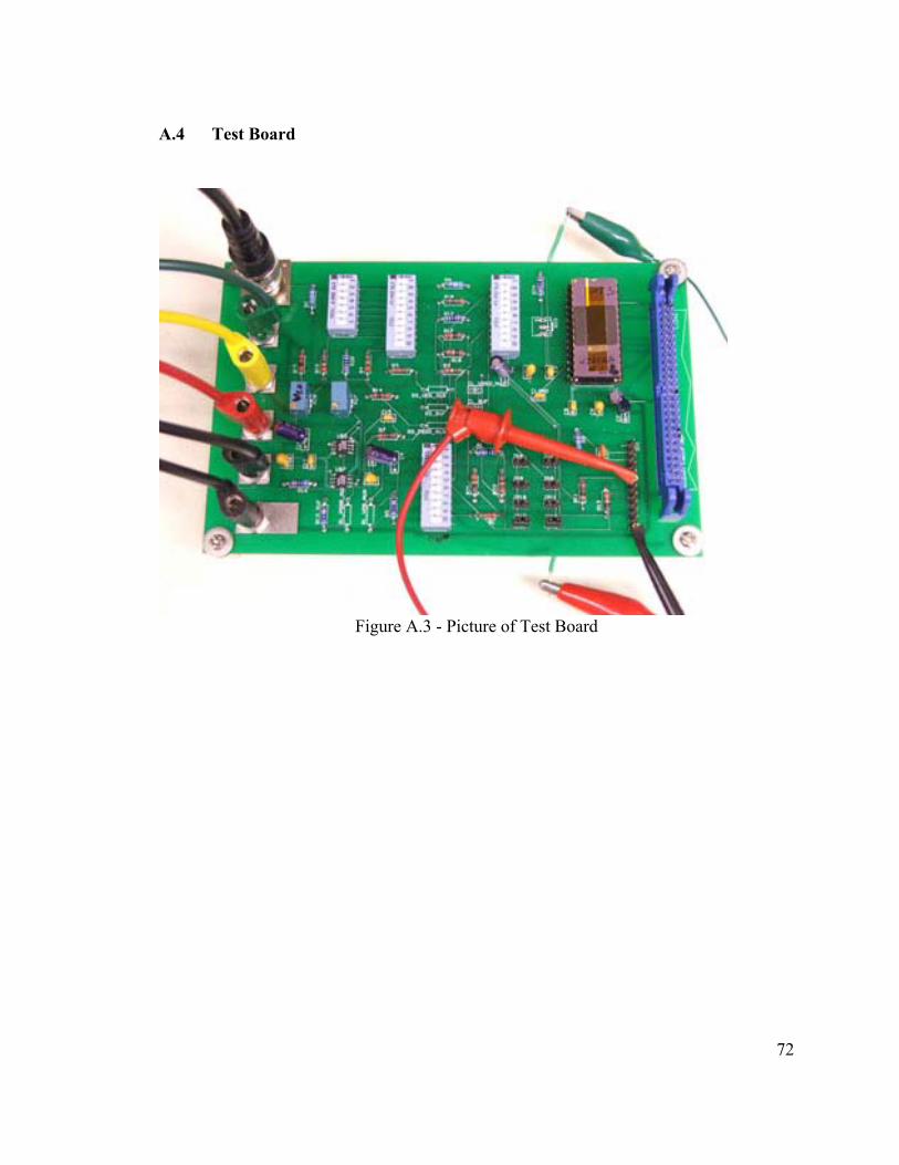
A.4 Test Board
Figure A.3 - Picture of Test Board
72
VITA
Chandradevi Ulaganathan was born in Pondicherry, India on January 20, 1980.
She grew up in Pondicherry and attended the St. Joseph of Cluny Higher Secondary
school. She obtained a Bachelor of Technology degree in Electronics and
Communication Engineering from Pondicherry University, India in May 2001. Then she
worked as a Software Engineer in Infosys Technologies for two years before moving to
United States to further her education. She obtained a Master of Science degree in
Electrical Engineering from the University of Tennessee, Knoxville in May 2007.
73
Related Documents