DEPOSITION OF SIZESELECTED NANOCLUSTERS by Lu Cao A thesis submitted to The University of Birmingham for the degree of Doctor of Philosophy Nanoscale Physics Research Laboratory School of Physics and Astronomy The University of Birmingham September 2015

Welcome message from author
This document is posted to help you gain knowledge. Please leave a comment to let me know what you think about it! Share it to your friends and learn new things together.
Transcript
DEPOSITION OF SIZE-‐SELECTED
NANOCLUSTERS
by
Lu Cao
A thesis submitted to The University of Birmingham for the degree of
Doctor of Philosophy
Nanoscale Physics Research Laboratory
School of Physics and Astronomy
The University of Birmingham
September 2015

University of Birmingham Research Archive
e-theses repository This unpublished thesis/dissertation is copyright of the author and/or third parties. The intellectual property rights of the author or third parties in respect of this work are as defined by The Copyright Designs and Patents Act 1988 or as modified by any successor legislation. Any use made of information contained in this thesis/dissertation must be in accordance with that legislation and must be properly acknowledged. Further distribution or reproduction in any format is prohibited without the permission of the copyright holder.
Abstract
The work presented in this thesis explores the production and the controlled
deposition of size-‐selected nanoclusters. The size-‐dependent propagation of gold
nanoclusters is investigated by depositing them through few-‐layer graphene
(FLG) using a magnetron sputtering cluster source. Au55 nanoclusters penetrate
through the FLG, however Au923 nanoclusters remain on the surface, as imaged
by aberration corrected scanning transmission electron microscope (ac-‐STEM).
The control of the atomic structure of gold nanoclusters (Au923) by
systematically varying the gas-‐phase condensation parameters in the magnetron
sputtering cluster source (e.g. magnetron power and condensation length) is also
reported. Results show we have the ability to eliminate all icosahedral isomers
by tuning the formation conditions. The biggest advance reported in the work
concerns the new technology of the Matrix Assembly Cluster Source (MACS),
which has the potential to increase the production rate of nanoclusters by 7
orders of magnitude from 0.1-‐1nA (from a magnetron source) to 1-‐10mA. The
principle of the MACS is demonstrated by the production of Ag and Au clusters.
The development of the latest MACS instrument is also described. An equivalent
cluster beam current of ~100nA has been achieved. Gold and silver clusters
produced under controlled experimental conditions show a relatively narrow
size distribution even without mass selection (at best ±25% in the number of
atoms). The mean cluster size can be controlled via the experimental
parameters, especially the metal concentration in the matrix. STEM is again the
principal tool employed characterize the number and structure of cluster
produced by the MACS.
Acknowledgements
I would like to thank many people for the help and support during my PhD life,
especially the following individuals.
Prof. Richard Palmer, my supervisor, for the opportunity to work in the NPRL
with such challenge but interesting project. Also thanks for providing me with
inspiration, advice and motivation throughout last four years.
Dr. Feng Yin, co-‐supervisor, for the continuous support and suggestions on the
all the works and other matters, without whom I cannot complete this thesis.
Dr. Simon Plant, co-‐supervisor, for the expertise and assistance on cluster source
and excellent comments on the draft of the thesis.
William Terry, for the irreplaceable technical support on the MACS project. Dr.
Zhiwei Wang, Miriam Dowle, and Dr. Kenton Arkill, for the patience and help on
the electron microscope.
Dr. Ziyou Li, Dr. Quanming Guo, Dr. Wolfgang Theis, Dr. Richard Balog, Dr. Vitor
Oiko, Dr. Karl Bauer, Nan Jian, Thibaut Mathieu, Jian Liu, Rongsheng Cai, Scott
Holmes, for the help in many areas related to the project.
All past and present colleagues, in particular Kuo-‐Juei Hu, whose consistent
friendship and support have been invaluable.

Author’s Contribution
All of the work presented in this thesis was conducted by the author under the
supervision of Prof. Richard Palmer and co-‐supervision of Dr. Feng Yin and Dr.
Simon Plant. The contributions between the author and collaborators are
described in full at the start of each chapter.
Author’s Publications
Plant, S. R., Cao, L., Yin, F., Wang, Z. W., & Palmer, R. E. (2014). Size-‐dependent
propagation of Au nanoclusters through few-‐layer graphene. Nanoscale, 6(3),
1258-‐1263.
Plant, S. R., Cao, L., & Palmer, R. E. (2014). Atomic structure control of size-‐
selected gold nanoclusters during formation. Journal of the American Chemical
Society, 136(21), 7559-‐7562.
Cao, L. et al., Matrix assembly cluster source (MACS) metal doping, In
preparation.
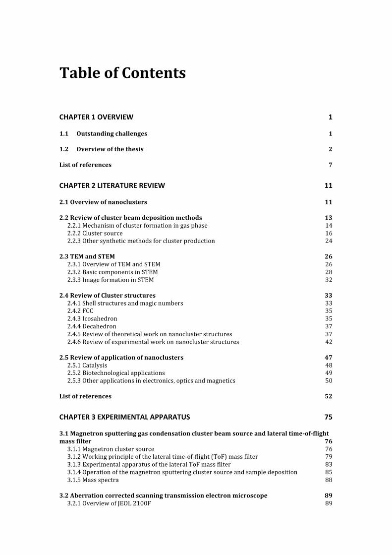
Table of Contents
CHAPTER 1 OVERVIEW 1
1.1 Outstanding challenges 1
1.2 Overview of the thesis 2
List of references 7
CHAPTER 2 LITERATURE REVIEW 11
2.1 Overview of nanoclusters 11
2.2 Review of cluster beam deposition methods 13 2.2.1 Mechanism of cluster formation in gas phase 14 2.2.2 Cluster source 16 2.2.3 Other synthetic methods for cluster production 24
2.3 TEM and STEM 26 2.3.1 Overview of TEM and STEM 26 2.3.2 Basic components in STEM 28 2.3.3 Image formation in STEM 32
2.4 Review of Cluster structures 33 2.4.1 Shell structures and magic numbers 33 2.4.2 FCC 35 2.4.3 Icosahedron 35 2.4.4 Decahedron 37 2.4.5 Review of theoretical work on nanocluster structures 37 2.4.6 Review of experimental work on nanocluster structures 42
2.5 Review of application of nanoclusters 47 2.5.1 Catalysis 48 2.5.2 Biotechnological applications 49 2.5.3 Other applications in electronics, optics and magnetics 50
List of references 52
CHAPTER 3 EXPERIMENTAL APPARATUS 75
3.1 Magnetron sputtering gas condensation cluster beam source and lateral time-‐of-‐flight mass filter 76 3.1.1 Magnetron cluster source 76 3.1.2 Working principle of the lateral time-‐of-‐flight (ToF) mass filter 79 3.1.3 Experimental apparatus of the lateral ToF mass filter 83 3.1.4 Operation of the magnetron sputtering cluster source and sample deposition 85 3.1.5 Mass spectra 88
3.2 Aberration corrected scanning transmission electron microscope 89 3.2.1 Overview of JEOL 2100F 89
3.2.2 Imaging 92 3.2.3 Effect of electron beam 95
3.3 Atom counting of clusters produced in MACS 98
List of references 105
CHAPTER 4 DEPOSITION OF SIZE-‐SELECTED GOLD NANOCLUSTERS 107
4.1 Size-‐dependent propagation 108 4.1.1 Overview 108 4.1.2 Sample preparation and implantation depth of nanoclusters into graphite 110 4.1.3 Controlled deposition of size selected Au55 and Au923 on FLG 113 4.1.4 Conclusion 120
4.2 Atomic structure control 121 4.2.1 Overview 121 4.2.2 Sample preparation 122 4.2.3 Variation of magnetron power 124 4.2.4 Variation of condensation length 127 4.2.5 Conclusion 130
List of references 132
CHAPTER 5 PROOF-‐OF-‐PRINCIPLE DEMONSTRATION OF THE MATRIX ASSEMBLY CLUSTER SOURCE (MACS) 139
5.1 Introduction of the MACS 140 5.1.1 Overview 140 5.1.2 Transmission and reflection mode 140 5.1.3 Methodology 142 5.1.4 Promising features and Potential of scaling-‐up 143
5.2 MACS demonstration apparatus 145 5.2.1 Matrix condensation support 146 5.2.2 Cryogenic cooling 146 5.2.3 Temperature measurement 147 5.2.4 Evaporation 147 5.2.5 Gas dosing 149 5.2.6 Ar ion beam 150
5.3 Sample preparation 151
5.4 Results and discussion 153 5.5.1 Demonstration of cluster production in MACS 153 5.5.2 Size distribution 154 5.5.3 Flux of clusters 155 5.5.4 Size control 156 5.5.5 Effects of beam energy 158 5.5.6 Improvements to increase cluster flux 160 5.5.7 Continuous production 162
5.6 Summary 164
List of references 166
CHAPTER 6 DEVELOPMENT OF THE MATRIX ASSEMBLY CLUSTER SOURCE (MACS) 169
6.1 Experimental apparatus of MACS 1 170 6.1.1 Overview 170 6.1.2 Cryocooler 173 6.1.3 Matrix condensation support 173 6.1.4 Evaporation 174 6.1.5 Ion source 175 6.1.6 Ion optics and SIMION simulations 176 6.1.7 Design of ion optics 179 6.1.8 Ar beam profile with ion optics 181
6.2 Ag clusters produced in MACS 1 182 6.2.1 Cluster flux 182 6.2.2 Large area coating using clusters produced in MACS 1 185 6.2.3 Size distribution 186 6.2.4 Size control 188 6.2.5 Different deposition time 191
6.3 Au clusters produced in MACS 1 192 6.3.1 Metal concentration 193 6.3.2 Matrix temperature 194 6.3.3 Effect of incident beam energy 196
6.4 Measurement of charge fractions 198
6.5 Mass spectroscopy of clusters produced in the MACS 203 6.5.1 Experiment setup 203 6.5.2 SIMION simulation 204 6.5.3 Mass spectra 206
6.6 Summary 208
List of references 210
CHAPTER 7 CONCLUSIONS AND OUTLOOK 214
1
Chapter 1 Overview
Nanoclusters are attracting great attention because of their size and structural
dependent properties as well as the interactions between nanoclusters and
surfaces, which give nanoclusters vast potential in various applications such as
catalysis [1-‐6], optical spectroscopy [7-‐9], nanoelectronics and biochips [10-‐12].
Deposition of nanoclusters on the surface offers a routine to control the
properties even for novel materials such as graphene. The developments on the
cluster beam and mass selection technologies provide the possibility to deposit
nanoclusters on surfaces under high control [13-‐15].
1.1 Outstanding challenges
Although the selection of the size of nanoclusters produced in the cluster beam
now permits the investigation of their size-‐dependent properties [16-‐22],
however, there are still many outstanding challenges remaining in this field. One
of the major challenges is even for a specific size, nanoclusters exhibit a range of
geometric structures as reported on size-‐selected gold nanoclusters containing
2
magic number of atoms such as 20, 55, 309 and 923 [23-‐26]. The ability to
control the isomer populations during formation of nanoclusters would enable
their properties to be correlated with their atomic configurations. Indeed, one
could argue that the combination of size-‐selection and atomic structural
determination would represent an “ultimate limit” of control at the nanoscale.
Another is the production rate of clusters by cluster beam deposition is limited
by the cluster beam flux. For example, the typical cluster beam current generated
in a magnetron sputtering gas condensation cluster source is limited to about
0.1-‐1nA, equivalent to only ~micrograms of clusters per hour [14]. This amount
is sufficient for demonstration purpose of nanoclusters, for example as model
catalysts. However, ~mg/day or even ~kg/day is the required economic
quantities for applications such as test-‐tube tests and pharmaceutical/ fine
chemicals application.
1.2 Overview of the thesis
In this thesis, we first explore the size dependent propagation of nanoclusters to
demonstrate the potential in generation of nanostructured membranes. Secondly
to overcome the “ultimate limit” challenge, condensation parameters in
magnetron sputtering source are investigated in order to control the structures
of nanoclusters. Finally, we report the progress on the proof-‐of-‐principle
demonstration and development of the new technology, the matrix assembly
cluster source, which has the potential to achieve abundant production of
nanoclusters. This work acts as the bridge connecting fundamental
demonstrations and practical applications of nanoclusters.
3
This thesis starts from the review of the related fields in Chapter 2 based on
which are the works presented in this thesis. This chapter includes the
introduction of the nanoclusters, production methods, characterization
approaches, review of nanolcuster structures and the applications of the
nanoclusters in variable areas. The introduction of nanoclsuters begins with the
definition of the nanoclusters and briefly summarizes properties of nanoclusters,
and their critical roles in variable applications. The review of nanocluster
production methods focuses on the cluster beam deposition (CBD) techniques
such as thermal source, laser ablation source and especially the magnetron
source. Other production methods like wet-‐chemical way are also introduced.
The characterization approaches reviewed in this chapter is focused on the
scanning transmission electron microcopy (STEM), which is the primary
characterization tool used for the works reported in this thesis. This part
includes the history of the TEM/STEM and the image formation mechanisms in
STEM. The review of nanocluster structure consists of the introduction of high
symmetrical structures which are icosahedral, decahedral and fcc, and both
theoretical calculations and experimental observations of cluster structures
reported in last few years. The application of nanoclusters part briefly describes
their utilizations especially in catalysis and biotechnologies.
The experimental apparatus used for the work in this thesis, such as the
magnetron sputtering gas condensation cluster source equipped with lateral
time-‐of-‐flight (ToF) mass filter and the aberration corrected scanning
transmission electron microscope (ac-‐STEM), are described in Chapter 3. The
schematics and basic components of both apparatuses are illustrated. The
4
operation of the magnetron source is introduced, with focus on how to optimize
the cluster beam current and mass spectra measurement (sections 3.1.4 and
3.1.5). The STEM part focuses on the high angle annular dark field (HAADF)
image and bright field (BF) image in section 3.2.2, both of which are used to
characterize the clusters. The effects of electron beam are reported in section
3.2.3.
Chapter 4 to 6 are the result parts of the thesis. The works reported in Chapter 4
are the deposition and structural control of size-‐selected nanoclusters produced
using the magnetron sputtering cluster source. The first part of the work
reported in Chapter 4.1 is the size dependent propagation study of Au
nanoclusters through few-‐layer graphene. Size-‐selected Au55 and Au923
nanoclusters, synthesized in the magnetron sputtering cluster source and size
selected by the lateral time-‐of-‐flight mass filter, were deposited onto the few-‐
layer graphene (FLG) surface [27]. The results show that clusters propagate
through the FLG via a mechanism of defect generation, which is strongly
dependent on cluster size. This approach provides an opportunity to control the
introduction of dopant nanoclusters and generation of nanoscale defects in
graphene or other thin membrane materials.
In the second part, in Chapter 4.2 we report the atomic structure control of size-‐
selected Au923 nanoclusters by variation of the formation conditions such as
magnetron power and condensation length [28]. Size-‐selected Au923 clusters
prepared using a magnetron sputtering gas condensation cluster source
exhibited three main high symmetry isomers: decahedral (Dh), icosahedral (Ih)
5
and face-‐centred cubic (fcc) structures such as the cuboctahedron.[26] The
identification of the proportions of Ih, Dh and fcc isomers of Au923 nanoclusters
within a given population, corresponding to a specific set of formation conditions
was achieved by comparing HAADF STEM imaging at atomic resolution with
multi-‐slice image simulations [24]. The results show we have the ability to tune
the cluster formation conditions in order to eliminate all icosahedral isomers,
which offers a route to the preparation of arrays or ensembles of supported
nanoclusters consisting of a dominant or only single isomer, thus enabling the
investigation of nanocluster properties as a function of not only the size but also
the atomic configuration.
In Chapter 5 and 6 we report proof-‐of-‐principle demonstration and progress on
the development of a new technology, the Matrix Assembly Cluster Source
(MACS). The working principle of the MACS is introduced in Chapter 5. The first
MACS apparatus was built and the proof-‐of-‐principle of the MACS was
demonstrated. Also the effects of different parameters on cluster size and flux
were preliminary studied in this chapter. In Chapter 6, we discuss the design and
construction of a new MACS system, MACS 1, to scale up the cluster production
rate as well as systematically investigated the effects of different parameters on
cluster production such as metal concentration, matrix temperature, incident
beam energy, so as to discover the cluster formation mechanisms. So far we have
achieved an equivalent cluster beam current of ~100nA. Results show that gold
and silver clusters produced under controlled experimental conditions show a
relatively narrow size distribution even without mass selection (m/Δm~1). The
mean cluster size can be controlled via experimental parameters, especially the

6
metal concentration in the matrix. Effects of other parameters such as matrix
temperature, incident beam energy on cluster size and flux are also investigated.
The charge fractions of the clusters were also studied and mass spectra were
obtained from the charged clusters using lateral time-‐of-‐flight mass selector,
further confirming the cluster production and size control in the MACS.
Chapter 7 summarizes the results from all the work and describes the future
plans both on fundamental demonstration of nanoclusters and instrument
development of the MACS.
The works presented in this thesis are under supervision of Prof. Richard Palmer
and co-‐supervision of Dr. Feng Yin and Dr. Simon Plant as well as a few of
collaborators. The respective contributions by the author and collaborators are
identified before each chapter.
7
List of references
[1] Herzing, Andrew A., et al. "Identification of active gold nanoclusters on iron
oxide supports for CO oxidation." Science 321.5894 (2008): 1331-‐1335.
[2] Häkkinen, Hannu, et al. "Structural, electronic, and impurity-‐doping effects in
nanoscale chemistry: supported gold nanoclusters." Angewandte Chemie
International Edition 42.11 (2003): 1297-‐1300.
[3] Tsunoyama, Hironori, et al. "Size-‐specific catalytic activity of polymer-‐
stabilized gold nanoclusters for aerobic alcohol oxidation in water." Journal of
the American Chemical Society 127.26 (2005): 9374-‐9375.
[4] Palomba, S., L. Novotny, and R. E. Palmer. "Blue-‐shifted plasmon resonance of
individual size-‐selected gold nanoparticles." Optics Communications 281.3
(2008): 480-‐483.
[5] Hu, Kuo-‐Juei, et al. "The effects of 1-‐pentyne hydrogenation on the atomic
structures of size-‐selected Au N and Pd N (N= 923 and 2057) nanoclusters."
Physical Chemistry Chemical Physics (2014).
[6] Habibpour, V., et al. "Novel powder-‐supported size-‐selected clusters for
heterogeneous catalysis under realistic reaction conditions." The Journal of
Physical Chemistry C 116.50 (2012): 26295-‐26299.
[7] Malola, Sami, et al. "Au40 (SR) 24 cluster as a chiral dimer of 8-‐electron
superatoms: Structure and optical properties." Journal of the American Chemical
Society 134.48 (2012): 19560-‐19563.
[8] Xie, Jianping, Yuangang Zheng, and Jackie Y. Ying. "Protein-‐directed synthesis
of highly fluorescent gold nanoclusters." Journal of the American Chemical Society
131.3 (2009): 888-‐889.
8
[9] Haes, Amanda J., and Richard P. Van Duyne. "A nanoscale optical biosensor:
sensitivity and selectivity of an approach based on the localized surface plasmon
resonance spectroscopy of triangular silver nanoparticles." Journal of the
American Chemical Society 124.35 (2002): 10596-‐10604.
[10] Wyrwa, Daniel, Norbert Beyer, and Günter Schmid. "One-‐dimensional
arrangements of metal nanoclusters." Nano Letters 2.4 (2002): 419-‐421.
[11] Partridge, Jim G., et al. "Formation of electrically conducting mesoscale
wires through self-‐assembly of atomic clusters." Nanotechnology, IEEE
Transactions on 3.1 (2004): 61-‐66.
[12] Palmer, Richard E., and Carl Leung. "Immobilisation of proteins by atomic
clusters on surfaces." TRENDS in Biotechnology 25.2 (2007): 48-‐55.
[13] Von Issendorff, B., and R. E. Palmer. "A new high transmission infinite range
mass selector for cluster and nanoparticle beams." Review of Scientific
Instruments 70.12 (1999): 4497-‐4501.
[14] Pratontep, S., et al. "Size-‐selected cluster beam source based on radio
frequency magnetron plasma sputtering and gas condensation." Review of
scientific instruments 76.4 (2005): 045103.
[15] Goldby, I. M., et al. "Gas condensation source for production and deposition
of size-‐selected metal clusters." Review of scientific instruments 68.9 (1997):
3327-‐3334.
[16] Baletto, Francesca, and Riccardo Ferrando. "Structural properties of
nanoclusters: Energetic, thermodynamic, and kinetic effects." Reviews of modern
physics 77.1 (2005): 371.
[17] Barnard, A. S. "Modelling of nanoparticles: approaches to morphology and
evolution." Reports on Progress in Physics 73.8 (2010): 086502.
9
[18] Barnard, Amanda S., et al. "Nanogold: a quantitative phase map." ACS nano
3.6 (2009): 1431-‐1436.
[19] Barnard, Amanda S. "Direct comparison of kinetic and thermodynamic
influences on gold nanomorphology." Accounts of chemical research 45.10
(2012): 1688-‐1697.
[20] Sanchez, A., et al. "When gold is not noble: nanoscale gold catalysts." The
Journal of Physical Chemistry A 103.48 (1999): 9573-‐9578.
[21] Maier, Stefan A., et al. "Plasmonics—a route to nanoscale optical devices."
Advanced Materials 13.19 (2001): 1501-‐1505.
[22] Wu, Yue, et al. "Controlled growth and structures of molecular-‐scale silicon
nanowires." Nano Letters 4.3 (2004): 433-‐436.
[23] Wang, Z. W., and R. E. Palmer. "Direct atomic imaging and dynamical
fluctuations of the tetrahedral Au 20 cluster." Nanoscale 4.16 (2012): 4947-‐4949.
[24] Wang, Z. W., and R. E. Palmer. "Experimental evidence for fluctuating, chiral-‐
type Au55 clusters by direct atomic imaging." Nano letters 12.11 (2012): 5510-‐
5514.
[25] Li, Z. Y., et al. "Three-‐dimensional atomic-‐scale structure of size-‐selected
gold nanoclusters." Nature 451.7174 (2008): 46-‐48.
[26] Wang, Z. W., and R. E. Palmer. "Determination of the ground-‐state atomic
structures of size-‐selected Au nanoclusters by electron-‐beam-‐induced
transformation." Physical review letters 108.24 (2012): 245502.
[27] Plant, Simon R., et al. "Size-‐dependent propagation of Au nanoclusters
through few-‐layer graphene." Nanoscale 6.3 (2014): 1258-‐1263.

10
[28] Plant, Simon R., Lu Cao, and Richard E. Palmer. "Atomic structure control of
size-‐selected gold nanoclusters during formation." Journal of the American
Chemical Society 136.21 (2014): 7559-‐7562.
11
Chapter 2 Literature review
This chapter reviews literatures on the fields related to the works presented in
the thesis, including the background of nanoclusters, production methods
especially cluster beam technology, introductions of TEM/STEM, a review of
theoretical and experimental work on nanocluster structures and applications of
the nanoclusters in variable areas.
2.1 Overview of nanoclusters
A nanocluster is an aggregation of atoms from a few tens to millions with a
diameter ranging from 0.2 to 20nm and has properties different from the bulk.
The field of cluster science was first established in early 80’s since the discovery
of magic numbers [1-‐3]. It was found that clusters consisting of certain numbers
of atoms exhibit particularly stable atomic and electronic configurations and are
therefore observed in higher abundance compared with other size clusters. For
example, 13, 20, 55, 309, 561, 923 are the magic numbers of gold clusters and
clusters containing these numbers of atoms are much more stable and more
easily produced in gas phase [4-‐9]. The population of magic numbers kept
12
increasing due to the discoveries of new stable structures both theoretically and
experimentally [10-‐12]. With the development of cluster deposition and
characterization methods such as scanning probing microscope (SPM),
transmission electron microscope (TEM) etc., the experimental and theoretical
work of cluster structures and related properties have emerged [13-‐16].
Clusters exhibit remarkable properties and have demonstrated their potential in
technological applications across a wide range of fields as their properties are
strongly dependent on their size [17-‐20]. Small clusters are widely used as
catalysts to accelerate and select chemical reactions and their catalytic activity is
found dependent on their size [21]. For example, Pt clusters deposited on MgO
surface are used as catalyst for the oxidization of carbon monoxide, which was
first demonstrated by U. Heiz et al. in 1999 [22]. The efficiency of CO2 production
(CO2 per Pt atom) varies greatly with the size of the Pt clusters. Similar to the Pt
clusters, small Au clusters can also be used as catalyst for oxidization of CO [23].
Moreover Au and Pt clusters can be used as catalyst for the oxidative
dehydrogenation of hydrocarbons such as propane [24]. In nanofabrications,
size-‐selected clusters are used as the mask for dry plasma etching to create
nanoscale structures on semiconductors surface, such as nanopillars on a silicon
surface demonstrated by Palmer and co-‐workers [25]. The silicon substrate is
etched by an ECR plasma of SF6, and the mean size of the pillar is determined by
the chemical species of the deposited clusters. For example, Au, Ag and Cu
clusters with the same diameter deposited on the substrate create pillars with
different sizes. In the biological field, large size-‐selected clusters deposited on
surfaces can function as the anchor sites for the immobilization, separation and
13
orientation of protein molecules due to the covalent bonds formed between
proteins and clusters, offering the opportunity to make microarray biochips [26-‐
27]. Additionally, clusters are widely used in optical devices for their function of
amplifying the signal [28-‐30]. For example, in Raman spectrum, the Raman
scattering cross sections are enhanced greatly if the analysed molecule is
absorbed on Ag clusters because of which the electronic properties of the
molecule are changed and the excitations in the molecule and metal enhance the
resonance and local electromagnetic fields [31-‐32].
2.2 Review of cluster beam deposition methods
Cluster beam deposition is an ultra clean process has incomparable advantages
in production of nanostructural materials and is of primary importance for the
development of nanotechnology in industry [33-‐36]. The cluster beam depositon
of nanoclusters has been demonstrated not only suitable for fundamental
research but also has the potential in scaling up the production rate of
nanoclusters with highly controlled properties [35][38-‐45].
The formation of nanoclusters in cluster beam deposition approach is in the gas
phase and the critical parameter is the cross section of collisions between gas
atoms, cluster atoms and clusters [46-‐48]. In a typical cluster source the clusters
are formed by cooling down atomic vapor with injected cold condensation gas
(e.g. helium), where the collisions promotes the atomic vapor to condense into
clusters. The size distribution of clusters produced in gas phase is determined
by several parameters such as the saturation of the atomic vapor and pressure
14
and flow rate of inert gas, as well as the condensation length [49-‐52]. The cluster
generation chamber usually can be cooled using liquid nitrogen to reach a
temperature below 100K to favor the condensation of large clusters [53]. The
flux and the size of clusters increase with a denser atomic vapor in certain range.
However, in some cases, the atomic vapor can be too dense to be cooled by the
inert gas flow. The pressure of gas in the condensation chamber also affects the
production and size distribution of clusters as high inert gas pressure boosts the
condensation of large clusters. The significant increase in the detection of
clusters at high condensation gas pressure is probably due to two reasons: (a)
more clusters are swept out of condensation chamber by higher gas flow, and (b)
the ionization efficiency of clusters is greatly increased at high pressure.
2.2.1 Mechanism of cluster formation in gas phase
The cluster formation process in the gas phase can be separated into two steps:
nucleation and growth [54]. At the nucleation stage two body and three body
collisions are eliminated, as the kinetic energy of atomic vapor is much higher
than the bonding energy. The classical nucleation theory can be used to explain
the nucleation model where the change of Gibbs free energy ΔG including
contribution of both surface and volume is considered. The change of Gibbs free
energy of system is
∆𝐺 = 4𝜋𝑟!𝜎 +4𝜋𝑟!
3 ∆𝐺!
15
where σ is the surface tension and ΔGv is the Gibbs energy per volume [54]. To
simplify the equation, the nucleus is treated as a perfect sphere with atomic
volume of VL and radius r. In the gas phase, the Gibbs energy per volume ΔGv is
∆𝐺! = −𝑘!𝑇𝑙𝑛(𝑃!/𝑃!)/𝑉!
where Pv and Ps are the pressure of vapor and saturation vapor at temperature T
respectively and kB is the Boltzman constant. The critical radius rc is the radius of
nucleus when system reaches the equilibrium state, dΔG/dr=0, and
𝑟! =2𝜎𝑉!
𝑘!𝑇𝑙𝑛(𝑃!𝑃!)
The nucleus is stabilized by evaporating atoms when r<rc and by growing bigger
to reduce the Gibbs free energy when r>rc [36]. At a certain temperature, the
critical radius varies with the vapor pressures and it decreases with the
increasing supersaturating pressure.
The growth model used to explain the growth of nanoclusters when r>rc. It
includes two mechanisms: surface growth by adsorption of atoms and
coalescence [55]. Surface growth usually induces chemical reactions or phase
change of the cluster surface as the cluster is already formed before atoms
approaching. Coalescence is that clusters growing by collision between clusters
via mechanism of Brownian motion [56]. At the early stage of cluster growth the
surface growth is important and keeps contributing throughout the entire
growth process. The whole growth process continues until the end of
16
condensation chamber and the surface growth mechanism is more dominant
according to simulation by Hihara and Sumiyama [56-‐57].
2.2.2 Cluster source
Generally, cluster beam source can be categorized based on the cluster
generation or beam formation mechanism such as thermal heating, laser
ablation, magnetron sputtering [36]. Except for the clusters produced by ion
sputtering, an ionization stage is mounted on the cluster source to produce
charged particles for size selection or controlled deposition [58].
Thermal heating
The working principle of the thermal heating cluster beam source is that
materials are heated in a high temperature crucible to generate an atomic vapor,
which is similar to molecular beam epitaxy (MBE), but using a higher intensity
thermal source [59-‐60]. The cluster formation process in the thermal heating
source is realized by mixing the atomic vapor with high-‐pressure condensation
gas.
A great example of thermal heating cluster source is the seeded supersonic
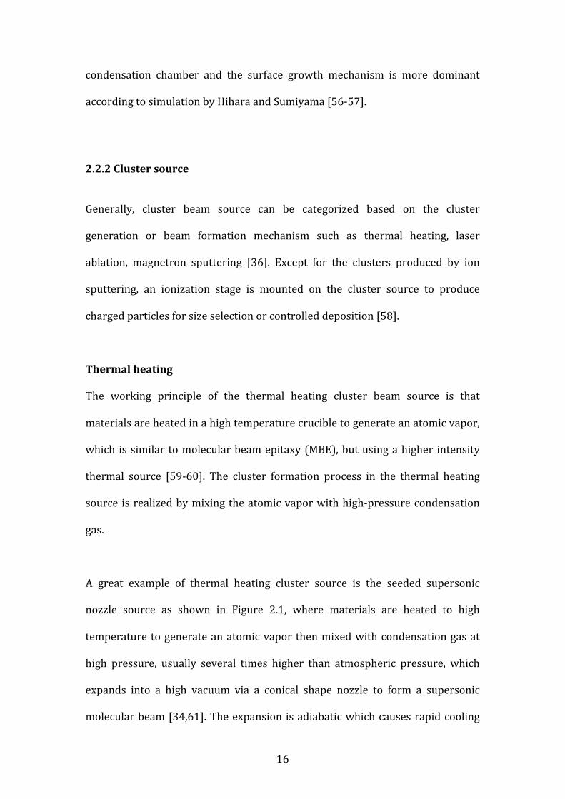
nozzle source as shown in Figure 2.1, where materials are heated to high
temperature to generate an atomic vapor then mixed with condensation gas at
high pressure, usually several times higher than atmospheric pressure, which
expands into a high vacuum via a conical shape nozzle to form a supersonic
molecular beam [34,61]. The expansion is adiabatic which causes rapid cooling
17
of the mixture of atomic vapor and inert gas. Clusters are formed from the
supersaturated atomic vapor and the growth process continues until far away
from the nozzle when the pressure of atomic vapor is too low for interactions to
take place between two clusters. Usually small clusters can be stabilized by the
cooling provided by the supersonic expansion, but it might be not enough for
large clusters such that evaporation of one or more atoms is inevitable for
stabilization.
Figure 2.1 Seeded supersonic nozzle cluster beam source, reproduced from
reference [34].
The seeded supersonic nozzle source is powerful enough to produce continuous
and intense cluster beams of up to 1018 atoms/s for low melting point materials
[62]. Because of the high consumption of material, most seeded supersonic
nozzle sources have a relatively large size oven to avoid frequent refilling, which
restricts the maximum temperature below 900K. The size of clusters produced in
this source is determined by several parameters such as the oven temperature,
inert gas pressure and the size of the nozzle. Usually the size of clusters
18
produced in the supersonic nozzle source ranges from two atoms to several
hundred atoms. Clusters with several thousand atoms were also reported for this
type of cluster source with very careful design and highly optimized
experimental conditions. Likewise the type of the condensation gas also affects
production and size of clusters. The growth of clusters lasts longer using a heavy
inert gas because of its large cross section of collisions. In summary, despite of
the high flux of clusters produced by the seeded supersonic nozzle source, this
source is restricted to the production of small size clusters from low melting
point materials (such as alkali metal). Also further ionization devices are needed
for size selection since the clusters produced based on this mechanism are
neutral.
Laser vaporization source
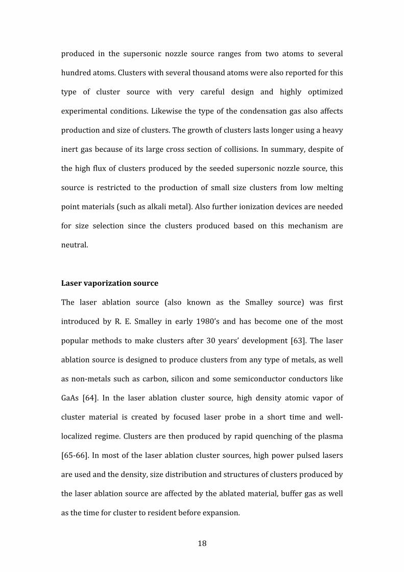
The laser ablation source (also known as the Smalley source) was first
introduced by R. E. Smalley in early 1980’s and has become one of the most
popular methods to make clusters after 30 years’ development [63]. The laser
ablation source is designed to produce clusters from any type of metals, as well
as non-‐metals such as carbon, silicon and some semiconductor conductors like
GaAs [64]. In the laser ablation cluster source, high density atomic vapor of
cluster material is created by focused laser probe in a short time and well-‐
localized regime. Clusters are then produced by rapid quenching of the plasma
[65-‐66]. In most of the laser ablation cluster sources, high power pulsed lasers
are used and the density, size distribution and structures of clusters produced by
the laser ablation source are affected by the ablated material, buffer gas as well
as the time for cluster to resident before expansion.
19
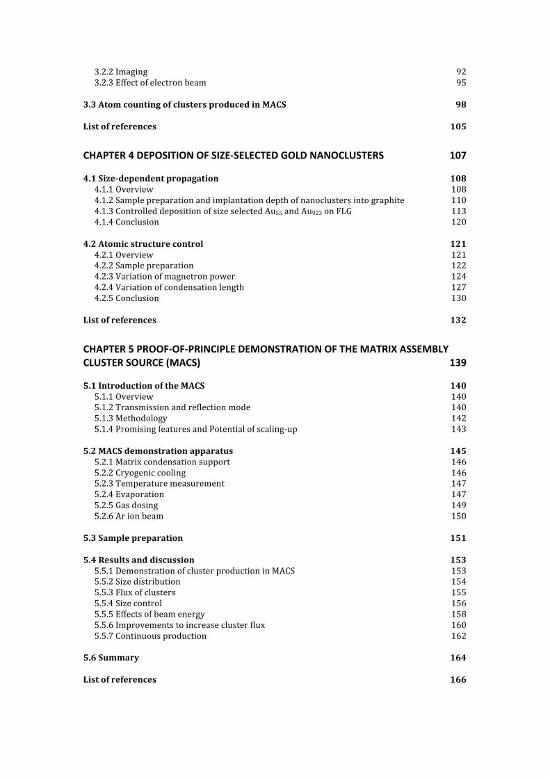
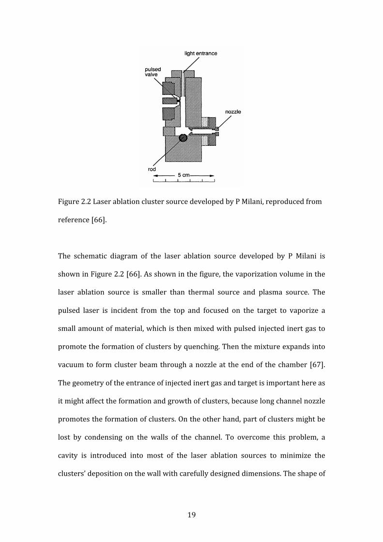
Figure 2.2 Laser ablation cluster source developed by P Milani, reproduced from
reference [66].
The schematic diagram of the laser ablation source developed by P Milani is
shown in Figure 2.2 [66]. As shown in the figure, the vaporization volume in the
laser ablation source is smaller than thermal source and plasma source. The
pulsed laser is incident from the top and focused on the target to vaporize a
small amount of material, which is then mixed with pulsed injected inert gas to
promote the formation of clusters by quenching. Then the mixture expands into
vacuum to form cluster beam through a nozzle at the end of the chamber [67].
The geometry of the entrance of injected inert gas and target is important here as
it might affect the formation and growth of clusters, because long channel nozzle
promotes the formation of clusters. On the other hand, part of clusters might be
lost by condensing on the walls of the channel. To overcome this problem, a
cavity is introduced into most of the laser ablation sources to minimize the
clusters’ deposition on the wall with carefully designed dimensions. The shape of
20
the target used in the laser ablation source varies, such as disc or rod. The target
is usually mounted on a rotation gear ensuring the uniform consumption of the
surface [68].
The size distribution of clusters produced in the laser ablation cluster source can
be controlled by the inert gas pressure and the condensation time of clusters
remaining in the source. It has been demonstrated that large amount of
monomers are formed at low gas pressure, while large clusters are more favored
at high pressure [69]. Conversely to the continuous beam produced by the
thermal evaporation, the laser vaporization source produces a pulsed beam but
the overall production is as high as the evaporation source. The material
consumption in the laser vaporization source is much lower because the use of a
pulsed laser avoids heating the sample continuously. Clusters can be produced
from a wider variety of bulk materials using laser vaporization, but the thermal
sources (evaporation source and supersonic source) are only restricted to low
melting point metals and few noble metals. With special design, some
complicated clusters can also be produced by using laser vaporization sources,
such as oxide, alloy and clusters surrounded with molecular ligands, produced in
a cutaway source (a special type of the laser vaporization source) [64,70].
Although the clusters produced by the laser vaporization source are probably
ionized during vaporization and collision processes, an ionization device is still
needed for the detection of clusters.
21
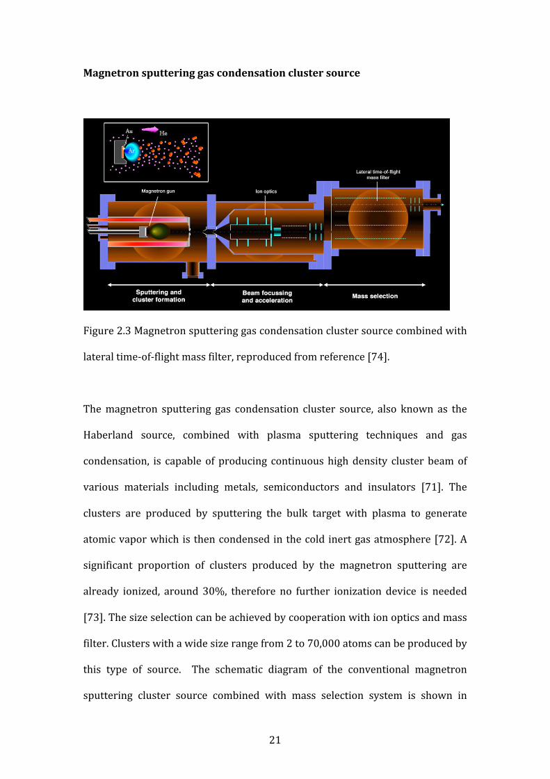
Magnetron sputtering gas condensation cluster source
Figure 2.3 Magnetron sputtering gas condensation cluster source combined with
lateral time-‐of-‐flight mass filter, reproduced from reference [74].
The magnetron sputtering gas condensation cluster source, also known as the
Haberland source, combined with plasma sputtering techniques and gas
condensation, is capable of producing continuous high density cluster beam of
various materials including metals, semiconductors and insulators [71]. The
clusters are produced by sputtering the bulk target with plasma to generate
atomic vapor which is then condensed in the cold inert gas atmosphere [72]. A
significant proportion of clusters produced by the magnetron sputtering are
already ionized, around 30%, therefore no further ionization device is needed
[73]. The size selection can be achieved by cooperation with ion optics and mass
filter. Clusters with a wide size range from 2 to 70,000 atoms can be produced by
this type of source. The schematic diagram of the conventional magnetron
sputtering cluster source combined with mass selection system is shown in
22
Figure 2.3 [74]. Typically it consists of three high vacuum chambers for cluster
generation, ion optics and mass selection respectively. Size selected clusters are
deposited onto a substrate in the deposition chamber mounted after the time-‐of-‐
flight mass selector.
The plasma sputtering takes place in an inner chamber, which can be cooled by
liquid nitrogen, inside the generation chamber. The target is mounted in front of
a magnetron gun, which is usually movable in a linear direction parallel to the
chamber’s axis allowing us to change the distance between the gun and the end
of the inner chamber. The sputtering gas is directly injected to the front of the
target from small orifices around the magnetron head. Both DC power and RF
power can be applied to the magnetron gun [75]. DC sputtering is only suitable
for conductive target because a large negative voltage is applied to the target
igniting Ar gas into plasma. The Ar plasma is always more positive charged than
negative because of its screening effect. The large negative voltage on the target
provides a strong electrical field accelerating Ar plasma to bombard the target.
For RF sputtering, both conducting and insulating targets can be used. The Ar gas
is ignited to form plasma by the RF high voltage coupled to the target. The high
RF voltage creates a cyclic attraction and repulsion of plasma on the target. This
causes more negative charges to remain on the target because of the greater
mobility of electrons building up a strong attraction to the positive plasma.
Supersaturated vapors of atomic ions as well as some small clusters are
produced in front of the target by the magnetron sputtering.
23
The condensation takes place in the rest of the inner chamber by introducing the
He gas. Clusters with a wide size distribution mixed with the gases leave the
inner chamber through an adjustable nozzle at the end. Given that 30% of
clusters are already ionized to the plasma, no further ionization device is needed
to generate an ion beam. The size range of clusters produced in the magnetron
sputtering source is determined at the condensation stage, which is mainly
affected by the gas pressure directly dominating the sputtering and
condensation processes [49,76]. Two different gases are used in the sputtering
gas condensation source: Ar and He. The Ar gas is used for the sputtering and
generally a higher Ar pressure induces a higher sputtering rate. Thus large
quantity of Ar gas is necessary to produce large clusters as they might require a
higher concentration of sputtered atoms. The effects of the He gas in the
magnetron sputtering source are more complicated. Similar to the inert gas in
other cluster sources, the He gas is responsible for the growth of clusters, which
provides cooling and collision for clusters condensation. Experimental results
show clusters produced without He gas in a magnetron sputtering source are
limited to a small size of 10 atoms or sometimes 20 atoms. The clusters growth
process in the magnetron sputtering sources can be simply divided into two
steps: sputtered atoms are cooled in He gas to form small cluster seeds; the
seeds then grow into large clusters by collision with other sputtered atoms and
small clusters [77]. Therefore, the He gas not only assists condensation of large
clusters from seeds by collision, but also creates seeds which are small clusters
[78]. The size distribution shifts towards smaller sizes when more seeds are
produced at high He pressure. Sputtering power and aggregation distance also
affects the size distribution. Inadequate sputtering power causes low production
24
rate of clusters and large clusters may not be formed. However, high sputtering
powers can be unstable and might lead to a discontinuous cluster beam. Clusters
are aggregated in the region between the magnetron gun and the nozzle. A
minimum distance of 10cm is required for plasma ignition. A large aggregation
distance in an optimum range enhances the production of large clusters.
The magnetron sputtering cluster source has several advantages over other
cluster sources. The clusters produced by magnetron sputtering are already
ionized at a notable proportion (~30%), such that the ion optics and mass filter
can be fitted directly after generation chamber. Compared with the seeded
supersonic nozzle source and evaporation source, clusters of a wide range of
materials and sizes can be produced by the magnetron sputtering source. Unlike
the pulsed beam used in the laser vaporization source, the cluster beam
produced by the magnetron sputtering source is continuous and the maximum
beam current of size selected cluster is up to several nano amps.
2.2.3 Other synthetic methods for cluster production
There are many other types of source apart from the thermal heating source,
laser ablation source and sputtering source to produce nanoclusters from a
physical vapour such as a pulsed microplasma cluster source and arc discharge
source. Compared with the sputtering source, a pulsed microplasma cluster
source is more suitable for stable operation as the atomic vapor is generated by a
spatially confined plasma ablation of the target and clusters are formed by
25
aggregation in pulsed injected inert gas phase [79-‐81]. However the critical issue
of the pulsed microplasma source is that the cluster beam flux is limited [46].
Another type of pulsed cluster source to produce highly ionized metal plasma is
the arc discharge source where a discharge happens between two conductive
electrodes to generate an atomic vapor. The arc discharge source has been
considered as the replacement of laser ablation source in 1990 by Meiwes-‐Broer
et al [82-‐83]. The principle of the vaporization by arc discharge is that large
current emitted from the cathode due to thermionic and field emission induces
the heating on the entire or small part of the cathode to vaporize materials. The
discharging current can reach up to 105A for short time intervals. Clusters are
formed by the vaporized materials or plasma which condense in the surrounding
buffer gas introduced from a pulse valve [84-‐85].
Also clusters can be produced by chemical synthesis in which metal or
semiconductor salts are used, and therefore it is versatile and usually
inexpensive compared with the physical routines [86-‐88]. The early study of
clusters produced via colloidal synthesis was reported by Faraday over 150
years ago [89]. Typically in chemical synthesis process nanoclusters are formed
in the supersaturated salt solutions which is reduced subsequently. The size,
shape and even crystalline of the nanoclusters can be controlled through the
conditions of the solution such as PH or concentration of the ions. The
nanoclusters synthesized in solution have great advantages if their applications
are required to be carried out in solutions [91].
26
2.3 TEM and STEM
2.3.1 Overview of TEM and STEM
The first transmission electron microscope (TEM) was developed my Nobel
Laureate (1986) Ernst Rusk and Max Knoll in 1932 where they successfully
transferred the principle of optic microscope to electrons [92]. The resolution
has been improved significantly with the electron microscope due to the
wavelength of electron is subnanometer instead of hundreds of nanometer of
visible light. Also the wavelength of electrons can be further shorten by
accelerating the electrons as the wavelength λ is determined by momentum of
the electrons p which follows the equation λ=h/p proposed by de Broglie in 1925.
According to the relativistic correction, the momentum of electrons is defined by
p=(2meV+eV2/c2)1/2 , thus wavelength of electron accelerated by 200kV is 10-‐
3nm [93]. The first scanning transmission electron microscope was developed
my Manfred von Ardenne in 1938 where the sample is raster by a focused
electron beam instead of the parallel electron beam in conventional TEM. The
development of the STEM has enabled various techniques in the electron
microscope such as annular dark field (ADF) imaging, Electron Energy Loss
Spectroscopy (EELS) and Energy Dispersive X-‐ray (EDX) mapping [94].
The spatial resolution of the STEM is defined by the tip size of the electron probe
on the sample, which is focused by objective lenses after electron gun and prior
to the sample [95]. In early days the resolution of the STEM was limited by the
positive spherical aberration when using round electron lenses pointed by
27
Scherzer [96]. To overcome this problem, the non-‐rotationally symmetric
corrector was introduced into the STEM by Scherzer in 1947, where a negative
aberration is generated deliberately to neutralize the positive aberration
induced by round lenses [97]. With the help of manufacture of the aberration
corrector, the resolution of STEM has been improved to a new era not only the
spatial resolution but also the depth sectioning resolution. The spatial resolution
of an state of the art STEM with aberration corrector has already been below 1
Angstrom and is pushing to nearly 0.5 Angstrom [98-‐99].
The great advantage of electrons is the wave-‐particle duality where the wave
behavior enables the formation of images and diffraction patterns revealing the
internal structures while the particle behavior facilities the interactions between
electrons and specimen exposing the chemical properties. Generally the electron
scattering can be divided into two groups, elastic scattering and inelastic
scattering or coherent scattering and incoherent scattering. The difference
between elastic and inelastic scattering the energy loss, which is important to
reveal the chemical properties of specimen. The coherent and incoherent
scattering is distinguished by whether the interference pattern can be formed by
the scattering waves. Most elastic coherent scattering happens with relatively
small scattering angles from 1 to 10 degree due to the Coulomb interaction
between the electron cloud and incident electron beam [93]. The differential
patterns, containing structure information of the material, are generated by the
coherent electrons plane penetrating the specimen that forming the secondary
spherical wavelets due to the low angle scattering by each atom. The high angle
scattering with angle more than 90 degree is usually incoherent caused by the
28
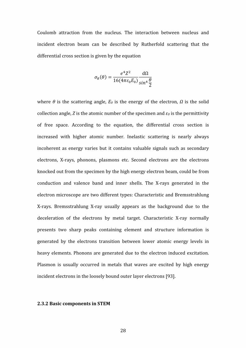
Coulomb attraction from the nucleus. The interaction between nucleus and
incident electron beam can be described by Rutherfold scattering that the
differential cross section is given by the equation
𝜎! 𝜃 =𝑒!𝑍!
16(4𝜋𝜀!𝐸!)dΩ
𝑠𝑖𝑛! 𝜃2
where θ is the scattering angle, E0 is the energy of the electron, Ω is the solid
collection angle, Z is the atomic number of the specimen and ε0 is the permittivity
of free space. According to the equation, the differential cross section is
increased with higher atomic number. Inelastic scattering is nearly always
incoherent as energy varies but it contains valuable signals such as secondary
electrons, X-‐rays, phonons, plasmons etc. Second electrons are the electrons
knocked out from the specimen by the high energy electron beam, could be from
conduction and valence band and inner shells. The X-‐rays generated in the
electron microscope are two different types: Characteristic and Bremsstrahlung
X-‐rays. Bremsstrahlung X-‐ray usually appears as the background due to the
deceleration of the electrons by metal target. Characteristic X-‐ray normally
presents two sharp peaks containing element and structure information is
generated by the electrons transition between lower atomic energy levels in
heavy elements. Phonons are generated due to the electron induced excitation.
Plasmon is usually occurred in metals that waves are excited by high energy
incident electrons in the loosely bound outer layer electrons [93].
2.3.2 Basic components in STEM
29
Electron gun
Nowadays most electron gun used in electron microscope is field emission gun
(FEG) instead of the thermionic source as electrons generated in FEG are more
monochromatic [93]. In the FEG electrons are generated by applying an intense
electrical field. Usually the electron gun is made of W or LaB6 etc, which have
high melting point or low work function that electrons can easily escape from the
conduction band. The electron gun is installed in an UHV chamber to avoid
contamination and oxidation. A typical FEG contains two anodes in front of the
gun which acts as the cathode. The first anode is biased to several thousand volts
relative to the electron gun tip providing the extraction field to attract electrons
out of the gun. The second anode is used to accelerate electrons also to make a
crossover of the electron beam working as an ion optic lens which affects the
electron beam size and position.
Magnetic lenses
In electron microscope magnetic lenses are used to focus electrons instead of
electrostatic lenses as they are not frightened to high voltage breakdown [93].
The movement of electrons in magnetic field is driven by Lorentz force F, which
follows the equation
𝐹 = −𝑒(𝐸 + 𝑣×𝐵)
where E is the strength of electric field, B is the strength of magnetic field and v is
the velocity of the electrons. The schematic diagram of a typical magnetic lens is
shown in Figure where a coil of copper wires is surrounded inside of the pole
piece made of soft iron. The magnetic field is created in the bore of the pole piece

30
by applying current through the coils. The strength of the magnetic field is not
homogeneous that it’s stronger close to the bore while it’s weaker in the center
and that’s how the focusing works by deflecting electron towards center less
than those away from the axis.
Resolution and Aberration correction
The theoretical resolution limit of the STEM can be calculated using the Rayleigh
criterion where the smallest resolvable distance δ is a function of the wavelength
of the incident radiation λ,
𝛿 ≈ 0.61𝜆
In the STEM, the incident radiation is the de Broglie wavelength of high energy
electron beam that
𝜆!" =ℎ
2𝑚𝑒𝑉(1+ 𝑒𝑉2𝑚𝑐!)
Therefore, the de Broglie wavelength of electron beam at V=200kV using this
equation is λdB=2.5x10-‐3nm, which giving a smallest resolvable distance
δ~1.5x10-‐3nm.
In reality, however, the imaging resolution in the STEM never reaches close to
the theoretical value and the main reason is the spherical aberrations. In the
STEM the spherical aberration is induced by the circular lenses as the focal point
of the electron beam varies with the distance from the center the lens. To
overcome this problem, the non-‐rotationally symmetric corrector was first
31
introduced into the STEM by Scherzer in 1947, where a negative aberration is
generated deliberately to neutralize the positive aberration induced by round
lenses.
Two different types of aberration correction systems are available commercially,
the multiple quadrupole and octupole lenses from Nion, which has the advantage
to correct the axial chromatic aberration but its non-‐rotationally symmetric
lenses are too complicated and hexapole and other transfer lenses from CEOS
where a round lens doublet is placed in the middle of a pair of hexapole lenses.
The principle of the aberration corrector is pre-‐diverge the electron beam to
compensate the aberration induced by objective lenses [100-‐102].
ADF and BF Detectors
Detectors in the electron microscope can be semiconductor detector, CCD
camera, scintillator-‐photomultiplier detector etc plus a viewing screen made of
doped ZnS to direct see the electrons via green fluorescence [93]. ADF detector is
the scintillator-‐photomultiplier detector coated with Al. Photons are generated
in the scintillator, normally made of Ce-‐doped yttrium-‐aluminium garnet, when
hit by incident electrons leading to the photoelectric effect at the entrance of the
photomultiplier tube (PMT) where electrons are multiplied up to 108. The
principle of BF detector is similar but using a round detector instead of the
annular detector. The collection angle of both ADF and BF detector are
determined and can be tuned by the electron optics after specimen such as
camera length. HAADF detector is the ADF detector but collecting high angle
scattered electrons.
32
2.3.3 Image formation in STEM
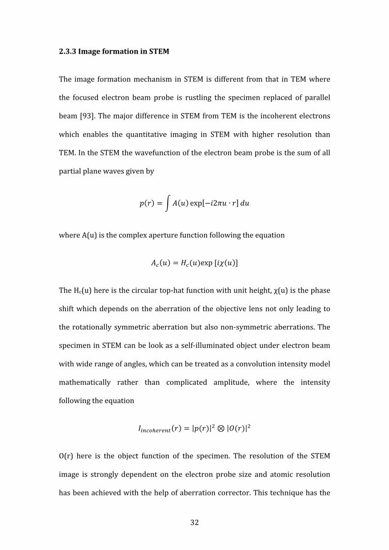
The image formation mechanism in STEM is different from that in TEM where
the focused electron beam probe is rustling the specimen replaced of parallel
beam [93]. The major difference in STEM from TEM is the incoherent electrons
which enables the quantitative imaging in STEM with higher resolution than
TEM. In the STEM the wavefunction of the electron beam probe is the sum of all
partial plane waves given by
𝑝 𝑟 = 𝐴 𝑢 exp −𝑖2𝜋𝑢 ∙ 𝑟 𝑑𝑢
where A(u) is the complex aperture function following the equation
𝐴! 𝑢 = 𝐻!(𝑢)exp [𝑖𝜒 𝑢 ]
The Hc(u) here is the circular top-‐hat function with unit height, χ(u) is the phase
shift which depends on the aberration of the objective lens not only leading to
the rotationally symmetric aberration but also non-‐symmetric aberrations. The
specimen in STEM can be look as a self-‐illuminated object under electron beam
with wide range of angles, which can be treated as a convolution intensity model
mathematically rather than complicated amplitude, where the intensity
following the equation
𝐼!"#$!!"!#$ 𝑟 = 𝑝(𝑟) !⊗ 𝑂(𝑟) !
O(r) here is the object function of the specimen. The resolution of the STEM
image is strongly dependent on the electron probe size and atomic resolution
has been achieved with the help of aberration corrector. This technique has the

33
advantage that intensity of the atomic column has linear relationship with its
thickness up to very large thickness which enables the date to be interpreted
more directly. The scattered electrons collected by ADF detector follow the
Rutherford scattering model where the intensity of the electrons is proportional
to Z2. However in reality, the power exponent is varied with camera length
between 2 and 1.5 due to the screening effect at low angles [103-‐106].
2.4 Review of Cluster structures
2.4.1 Shell structures and magic numbers
The Mackay icosahedral is a great example explaining the shell structure [107],
where 12 atoms are arranged to surround the central atom or all atoms are at
the corners of an icosahedral, which contains two shells for the former and only
one shell for the latter. In both cases, another layer of 42 atoms can be added on
top of these 13 atoms core again to form a larger perfect icosahedral consisting
of 55 atoms, which is known as one of the magic numbers of the Mackay
icosahedral and experimentally agrees well with rare gas clusters [108-‐109].
Another example is the tetrahedron, where 4 atoms compose the core or the first
shell. However unlike the icosahedron, adding one more complete layer to the
tetrahedron actually results in four more shells instead of one.
As mentioned before, the discovery of magic number boosts the development of
cluster science. Magic number is the total number of atoms consisted in a more
favored structure and geometrically a complete shells set. The Shell index K is
34
used to define the number of shells in a specific geometry and the central atom is
labeled with K=1 [110]. The equation of total number of atoms in most
commonly observed geometries as a function of shell number is summarized
below [111].
𝑛 =16𝐾
! +12𝐾
! +13𝐾 (𝑡𝑒𝑡𝑟𝑎ℎ𝑒𝑑𝑟𝑜𝑛)
𝑛 =103 𝐾! − 5𝐾! +
113 𝐾 − 1 ( 𝑀𝑎𝑐𝑘𝑎𝑦 𝑖𝑐𝑜𝑠𝑎ℎ𝑒𝑑𝑟𝑜𝑛)
𝑛 =56𝐾
! +16𝐾 (𝑑𝑒𝑐𝑎ℎ𝑒𝑑𝑟𝑜𝑛)
𝑛 =103 𝐾! − 5𝐾! +
113 𝐾 − 1 (𝑡𝑟𝑢𝑛𝑐𝑎𝑡𝑒𝑑 𝑑𝑒𝑐𝑎ℎ𝑒𝑑𝑟𝑜𝑛)
𝑛 =23𝐾
! +13𝐾 (𝑜𝑐𝑡𝑎ℎ𝑒𝑑𝑟𝑜𝑛)
𝑛 =103 𝐾! − 5𝐾! +
113 𝐾 − 1 (𝑐𝑢𝑏𝑜𝑐𝑡𝑎ℎ𝑒𝑑𝑟𝑜𝑛, 𝑡𝑟𝑖𝑎𝑛𝑔𝑢𝑙𝑎𝑟 𝑓𝑎𝑐𝑒𝑠)
𝑛 = 16𝐾! − 33𝐾! + 24𝐾 − 6 (𝑐𝑢𝑏𝑜𝑐𝑡𝑎ℎ𝑒𝑑𝑟𝑜𝑛, ℎ𝑒𝑥𝑎𝑔𝑜𝑛𝑎𝑙 𝑓𝑎𝑐𝑒𝑠)
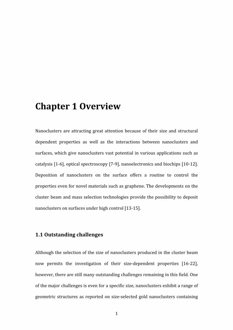
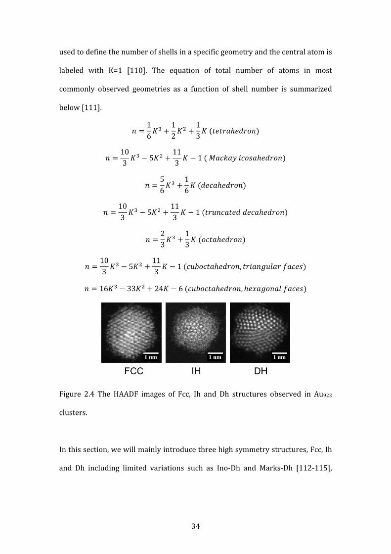
Figure 2.4 The HAADF images of Fcc, Ih and Dh structures observed in Au923
clusters.
In this section, we will mainly introduce three high symmetry structures, Fcc, Ih
and Dh including limited variations such as Ino-‐Dh and Marks-‐Dh [112-‐115],
35
which are the dominant proportions observed in our structure control work on
size selected Au923 nanoclusters as shown in Figure 2.4.
2.4.2 FCC
Fcc is the most closed parking (0.74) and most common structure observed in
bulk crystals. Nanoclusters with fcc structures can be treated as a fraction of the
bulk. Fcc exhibiting in nanoclusters or microscale particles via controlled growth
contains various geometries such as cube, truncated cube, cuboctahedraon,
truncated octahedron and octrahedraon. The Wulff construction, proposed by
Marks [115], is believed to be the role followed by nanoclusters in equilibrium
state fulfilling the equation [116],
𝛾 100𝛾(111) =
𝑑(100)𝑑(111)
where γ(100) and Υ(111) are the surface energy of (100) and (111) facets and
d(100) and d(111) are the corresponding distance between the facets and the
center of cluster. Different geometries with fcc structures are able to transfer
from one to another via mechanism of selective growth of cutting on specific
facets and the shape of face of all fcc geometries are limited to square, triangle
and hexagonal [116].
2.4.3 Icosahedron
36
Icosahedron clusters with 12 5-‐fold axes are never expected to grow to crystals
as it doesn’t match with the translational crystal symmetry. However,
microscope studies by Ino et al. have shown the observed icosahedral gold
nanoclsuters contain six 20 tetrahedra, which can be cut from fcc structure,
sharing a common vertex in the center [112]. As tetrahedral is not the space
filling structure, in the icosahedral nanoclusters the tetrahedral units usually
have twin boundaries with the neighboring units (multi twinned particles)
where the (111) facets of tetrahedra are exposed and crystallographical (111)
facets are shared by two adjacent tetrahedral units, which makes to the inner
three sides of each tetrahedral units are about 5% shorter than the side of
tetrahedral units on the surface [117]. The icosahedral structure in nanoclusters
was first reported by Mackay over 50 years ago when two icosahedral shell
structures were introduced, Mackay icosahedral and double Mackay icosahedral
and the latter has been corrected to anti-‐Mackay in early 2000’s by Kuo et al.
[118]. The Mackay and anti-‐Mackay are distinguished by the positions of the
landed the adatoms. For Mackay icosahedron, adatoms are deposited on the site
of FCC while for anti-‐Mackay adatoms are placed on HCP (hexagonal closed
parked) [118]. Icosahedral is energetically favored at the early stage of cluster
formation as reported based on calculations by theorist and the formation
mechanism of icosahedral by rapiding cooling, freezing and melting has been
argued for long time [119-‐122]. Baletto et al. have shown the theoretical study of
growth of silver clusters where icosahedral can be formed at low temperature
but then transform to decahedral due to thermal annealing [123]. In addition to
the Mackay and anti-‐Mackay icosahedral, a large amount of variants have been
found and reported in literature, such as Chui icosahedral where the icosahedral
37
decorated with crater on each corner and it is suggested to be more stable and
thermodynamically realistic especially for large size clusters [124-‐126].
2.4.4 Decahedron
Apart from the icosahedral, another 5-‐fold symmetry structure often observed in
nanoclusters is the decahedral. The regular decahedral consists of five
tetrahedral units which are packed together and four equilateral triangle (111)
facets of each tetrahedral are slightly distorted that two of these facets are
shared with other units as twinning planes while the other two are turned into
the surface of the decahedral [127]. The strain energy in decahedral is lower
compared with that in icosahedral owing to the lower strain in tetrahedral units.
Also the stain energy in decahedral can be minimized by varying the shape and
size of the units. For example, the regular decahedral is not favorable in the
experiments as it’s non-‐spherical shape [128]. Although the atoms on the regular
decahedral surface are closely-‐packed, the surface area of the decahedral is
extremely large besides the internal strain. However, the decahedral can be
truncated to become more spherical such as Ino-‐decahedral and Marks-‐
decahedral that have been observed experimentally in nanoclusters. (100) facet
are exposed on the truncated surface instead of closely-‐packed facets.
2.4.5 Review of theoretical work on nanocluster structures
The structure preference in nanoclusters is determined by the energetics
especially for the structures with lower energy. From theoretical calculations
38
reported in literature by Baletto and Ferrando [129], the common investigation
of the most favored structures in nanoclusters can be divided into two steps.
Firstly a model is introduced to represent the interactions between the
elementary constituents in the clusters where the Schrodinger equation is solved
directly and the constructions of semi-‐empirical inter-‐atom potentials are
involved. Secondly, a global optimization algorithm is applied to seek for the
most favored isomers [116].
The most critical part here is the choice of the energetic model, which directly
affects the accuracy of the calculation and there is not an ideal model that could
deal with all the cases. For example, the ab initio quantum chemistry method
provides exact solutions for most of the small clusters but it becomes
unmanageable with increasing the nanocluster size . Methods based on density
functional theory (DFT) are widely used in the structural calculations since
1990s and are believed to be accurate and less cumbersome after adequate test
[116]. Although the exchange and correlation interactions in the DFT methods
are refined approximately and greatly, there are still limitation for the DFT such
as the lacking of intermolecular interactions in which case the position of atoms
or molecules are not replaceable and the exclusion of thermodynamics, which
means all the calculations are run at 0K. Semi-‐empirical methods, improved from
the Hartree-‐Fock formalism that have been successfully used in organic
chemistry before, are now also used to build the approximate energetic models
in nanostructures [130]. For semiconductors and metals, there is the tight-‐
binding model method with intermediate computational effort based on the
wave functions [131]. The potentials between atom and atom or molecule and
39
molecule calculated based on the approximate quantum models can be then used
in large clusters or large crystals by fitting with experimental properties of the
materials via several methods such as EAM (embedded atom method), SMATB
(second movement approximate to tight binding) or Sutton-‐Chen potentials
[133]. The binding energy of a cluster can be described by the equation,
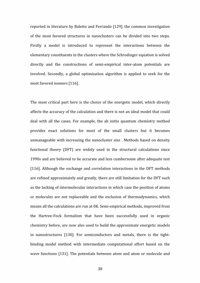
𝐸!"#!"#$ = 𝑎𝑁 + 𝑏𝑁! ! + 𝑐𝑁! ! + 𝑑
where N is the total number of the atoms containing in the cluster. The first term
aN is attributed to the volume effect and the rest of the equation corresponds to
the surface effect of facets bN2/3, edges cN1/3 and vertices d. Δ(N) is introduced to
represent the stability of the clusters by figuring out the excess energy per
surface atom with total N atoms in the perfect crystal,
𝛥 𝑁 =𝐸!"#$"#% − 𝑁𝜀!
𝑁!/!
where εc here is the cohesive energy per atom in the crystal [116].
EAM is one of the popular theoretic method reported by many scientists such as
Grocholar, Feiglto et al. to simulate the initial nucleation, coalescence and growth
kinetics especially for gold nanoclusters synthesized in gas phase [134]. The
simulations based on the EAM method have shown that the coalescence prefers
to form decahedral and fcc structures for gold nanoclusters of less than 300
atoms at the early stage. Other parameters like aggregation rate and type of
condensation gas do not affect the statistical structures much. The EAM
simulations also show the probability to form icosahedral structure is highly
40
related to the size of the initial seed and temperature, and it decreases with
increasing seed size whilst increased with raising temperature [135].
An interesting study of nanoclusters growth in liquid using both Molecular
Dynamics and hybrid Monte Carlo method are reported by Desgranges and
Delhommelle to simulate the nucleation of gold nanoclusters, where the growth
of the nanocluster is attributed to the continuous cross-‐nucleations of two
polymorphs [136]. They also found the nanoclusters are dominated by fcc
structures at small size but when it’s approaching the critical size, HCP
structures start nucleating on the surface heterogeneously [137]. The famous
microscopic mechanism study on growth of nanoclusters reported by Baletto et
al., has indicated the icosahedral and decahedral are more favored in
nanocrystalline structures of meta-‐stable silver nanoclusters at low and
intermediate temperature between 350K and 500K. The icosahedral isomers are
formed via the mechanism of shell by shell growth mode or the structural
transformation from decahedral [123]. In Baletto’s other work, silver
nanoclusters with different size up to about 150 atoms are studied showing at
extreme temperatures (both high and low) icosahedral is more preferred while
decahedral is favored at the intermediate range [138]. It has also been presented
that for gold nanoclusters where the immersion environment is found to have
effects on the growing process [139].
When size of nanoclusters increases, the effect of the strain especially for multi-‐
twinned nanoclusters becomes notable. Theoretical studies based on the surface
energy, boundary energy and elastic strain energy including Ino’s calculation
41
show that icosahedral gold nanoclusters are stable when size is smaller than
43.6nm whilst decahedral is 396.1nm [112]. Surface disorder also plays a critical
role in the structures of nanoclusters as reported by Chui et al [126].
Simulations based on the energetics of nanoclusters by Baletto et al., predicted
the structural transformations among icosahedral, decahedral and fcc in gold
nanoclusters, that is icosahedral starts transforming into decahedral or fcc when
the size of nanocluster is less than 100 atom and the transformation from
decahedral to fcc starts at about 500 atoms [129]. Similar to gold, Ni icosahedral
nanoclusters follow the same trend with increasing cluster size as investigated
by Cleveland et al. The phase map of gold nanoclusters less than 30nm in
diameter was calculated by Baletto et al. based on the first principle [127,140].
Also the roles of the substrate on nanoclusters structure cannot be neglected, for
example transformation from decahedral to icosahedral is observed on clusters
deposited on silica surface [20, 141].
Heating also plays a role in the structural transformation in nanoclusters
because cluster surface softens upon heating, reconstruction happens during the
heating and a liquid skin or quasi-‐molten state might be formed before the
clusters are fully melted [142-‐145]. Pt and Pd nanoclusters have been studied as
examples for heating effects based on EAM simulations by Schebarchov et al.,
which show the decahedral isomers of Pt887, Pt1389 and Pd887 is turned into fcc
before the melting point [146-‐147]. On the contrary, the freezing process is
intended to form icosahedral as explored by Chushak on Au1157 with a cooling
rate of 3x10¹¹ K/s [148]. The structures based on crystallization process are also
42
investigated by various groups showing crystallization starting at the surface
dominates the later crystallization process [149-‐151].
2.4.6 Review of experimental work on nanocluster structures
Most of the observations of structures of nanoclusters in experiments are
achieved by electron microscope including transmission electron microscope
(TEM) and scanning transmission electron microscope (STEM) both of which
have ability to resolve the structures at atomic level. Some large clusters are
studied in SEM as well. For gold nanoclusters, the first experimental observation
of the structure can be tracked back to 1960s where gold clusters with diameter
of about 30nm prepared by atomic vapor on gold single crystal were studied in
TEM by Schwodebel et al. and the structure observed is decahedral [152]. In
1966 Ino et al. started to investigate gold clusters with different size in TEM. The
clusters were prepared by atomic vapor deposition but with more control of the
growth. Results showed that gold clusters with decahedral were observed at size
of 40nm in diameter but icosahedral isomers were found as well with size
between 10-‐40nm [153]. The structures of supported multi-‐twinned gold
clusters on alkalihalide crystals were studied by Ino and Ogawa in 1967
suggesting that clusters of about 30nm prefer to be decahedral while 15nm
clusters prefer icosahedral [154]. Big gold clusters up to 500nm deposited on
mica substrate were also studied in early years by Sanders et al. showing
decahedral structure [155]. Tsutomu et al. also studied the structure of gold
clusters prepared by evaporation in TEM and the observation of decahedral for
15nm clusters and icosahedral for 13nm clusters was reported [156]. Between
43
1969 and 1972 the formation of multi-‐twinned gold clusters was investigated by
Ino and Ogawa who found decahedral structure on clusters with 15nm and 20-‐
40nm while icosahedral structure on 10 and 15-‐30nm clusters [157-‐158].
Wayman has studied structrure of gold clusters vaporized on graphite surface
and found both decahedral and icosahedral structures on clusters about 40nm
[159]. Relatively small gold clusters prepared by atomic vapor deposition were
studied by Gillet et al. in 1977 showing decahedral structure on 15nm clusters
and icosahedral structure on 8nm clusters [160]. Yacaman et al. reported the
experimental study of gold clusters by vapor deposition in 1979 showing the
decahedral structures of clusters between 12-‐40nm [161]. The first study of
structures of clusters produced by cluster beam was reported in 1981 by Gillet et
al. where Au, Pt and Pd clusters were produced in a flowing argon system and
gold clusters presented decahedral and icosahedral for 6nm and 7nm clusters
respectively [162]. In 1983 the Marks decahedral was first introduced by L. D.
Marks observed on 10nm gold clusters [115]. Hofmeister et al. explored the inter
structure of muli-‐twinned gold clusters on silver bromide film showing the gold
clusters were decahedral [163]. Berriel-‐Valdos et al. found the equilibrium
structure of 30nm gold clusters was icosahedral [164]. Ichihashi et al. studied
the small gold nanoclusters around 2.5nm in TEM showing the decahedral
structures [165]. Weiss et al. explored the structure of small gold nanoclusters
between 2 and 6nm and also observed decahedral structures [166]. In Yacaman’s
work in early 1990s where small gold nanoclusters were produced by gas
aggregation, decahedral structures were observed on 4nm gold clusters [167].
The structures of gold clusters prepared chemically were also studied where the
size of the clusters was relatively larger. In 1973 Suito et al. observed decahedral
44
structure in 30nm colloidal gold clusters in TEM [168]. In 1990 Tholen et al.
found gold clusters around 65nm synthesized chemically exhibiting decahedral
structures [169]. Tanaka et al. explored gold nanoclsuters chemically
synthesized in solution by electrodeposition with different electrode potentials
showing that multi-‐twinned structures such as decahedral and icosahedral are
more favored at low electrode potential and single crystalline or polycrystalline
are preferred at high potential [170].
In recent researches published since 2000, Hofmeister et al. studied chemically
synthesized gold nanoclusters containing two icosahedral in twin position in
TEM combined with computer simulations [171]. In Oku and Hiraga’s research
published in 2000, Au nanoclusters prepared by chemical vapor and gas
condensation with different size were studied in TEM, SEM and HREM and
decahedral structures were observed on Au clusters of about 5nm [172]. The
work done by Ugarte et al. in early 2000s has shown the statistical data of
structures of gold nanoclusters prepared chemically where gold nanoclusters in
range of 2-‐4nm were studied in HRTEM and XRD and fcc and decahedral
structures were observed [173]. Also Koga and Sugawara have done statistical
analysis on structures of gold nanoclusters with different size between 8 and 9
nm produced by cluster beam in HRTEM combined with multislice simulations
where both decahedral and icosahedral isomers were identified [174]. Gold
nanoclusters are used as catalyst and the structures of gold catalyst before and
after reaction were studied by Hofmeister and Claus et al. using HRTEM where
both decahedral and icosahedral were found on 5nm gold nanoclusters [175].
Buriak studied large gold nanoclusters of about 100nm synthesized chemically
45
in SEM which shows the large icosahedral structure [176]. Even larger gold
clusters from 200nm to 5micrometers were studied by Xie et al. where most of
them exhibit decahedral structures [177]. Chemically prepared small gold
nanoclusters with narrow size distribution, around 2nm, were studied by Perez
et al. showing that fcc and decahedral were dominant in Au clusters [178]. Using
chemical method, Han et al. tried controlled synthesis process to produce pure or
large proportion of gold clusters between 10 and 90nm with icosahedral
structures [179]. In addition to Han’s work, Song et al. have achieved the size
control on not only just icosahedral but also decahedral and truncated
tetrahedral gold clusters around 100nm prepared via chemical methods [180].
Moreover, Zhang et al. reported the ability to transform the structure of gold
clusters from icosahedral to a truncated form [181]. Li et al. studied the size
selected Au923 produced in magnetron sputtering gas condensation cluster beam
source in STEM where the decahedral structure is observed and its 3D structure
is revolved using quantitative HAADF image [4]. The effects of coalescence
behavior on gold nanoclusters of around 3nm was studied by Geng et al. which
promotes that formation of decahedral [182]. The coalescence of large cluster of
about 10nm was studied by Tilley where real time TEM and kinetic monte carlo
calculation were used to confirm decahedral is more favored in coalescence
behavior [183]. Lee et al. reported the ability to control the structure of large
gold clusters between 15-‐30nm in solution using 1,2-‐hexadecanediol to reduce
the AuCl4-‐, which determined the crystallinity of the cluster [184]. Yacaman et al.
studied the stability of decahedral in large clusters synthesized via rapid cooling
mechanism [185].
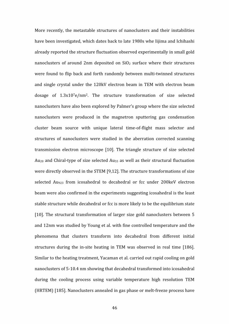
46
More recently, the metastable structures of nanoclusters and their instabilities
have been investigated, which dates back to late 1980s whe Iijima and Ichihashi
already reported the structure fluctuation observed experimentally in small gold
nanoclusters of around 2nm deposited on SiO2 surface where their structures
were found to flip back and forth randomly between multi-‐twinned structures
and single crystal under the 120kV electron beam in TEM with electron beam
dosage of 1.3x10⁷e/nm2. The structure transformation of size selected
nanoclusters have also been explored by Palmer’s group where the size selected
nanoclusters were produced in the magnetron sputtering gas condensation
cluster beam source with unique lateral time-‐of-‐flight mass selector and
structures of nanoclusters were studied in the aberration corrected scanning
transmission electron microscope [10]. The triangle structure of size selected
Au20 and Chiral-‐type of size selected Au55 as well as their structural fluctuation
were directly observed in the STEM [9,12]. The structure transformations of size
selected Au923 from icosahedral to decahedral or fcc under 200keV electron
beam were also confirmed in the experiments suggesting icosahedral is the least
stable structure while decahedral or fcc is more likely to be the equilibrium state
[10]. The structural transformation of larger size gold nanoclusters between 5
and 12nm was studied by Young et al. with fine controlled temperature and the
phenomena that clusters transform into decahedral from different initial
structures during the in-‐site heating in TEM was observed in real time [186].
Similar to the heating treatment, Yacaman et al. carried out rapid cooling on gold
nanoclusters of 5-‐10.4 nm showing that decahedral transformed into icosahedral
during the cooling process using variable temperature high resolution TEM
(HRTEM) [185]. Nanoclusters annealed in gas phase or melt-‐freeze process have
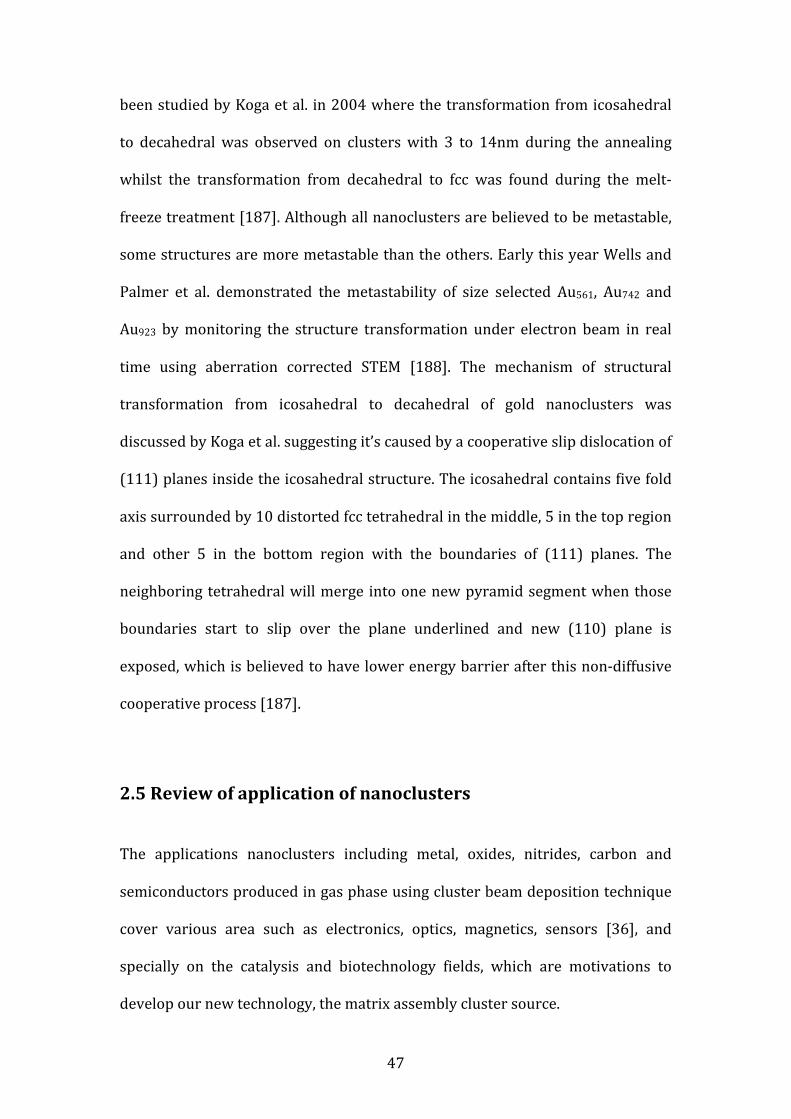
47
been studied by Koga et al. in 2004 where the transformation from icosahedral
to decahedral was observed on clusters with 3 to 14nm during the annealing
whilst the transformation from decahedral to fcc was found during the melt-‐
freeze treatment [187]. Although all nanoclusters are believed to be metastable,
some structures are more metastable than the others. Early this year Wells and
Palmer et al. demonstrated the metastability of size selected Au561, Au742 and
Au923 by monitoring the structure transformation under electron beam in real
time using aberration corrected STEM [188]. The mechanism of structural
transformation from icosahedral to decahedral of gold nanoclusters was
discussed by Koga et al. suggesting it’s caused by a cooperative slip dislocation of
(111) planes inside the icosahedral structure. The icosahedral contains five fold
axis surrounded by 10 distorted fcc tetrahedral in the middle, 5 in the top region
and other 5 in the bottom region with the boundaries of (111) planes. The
neighboring tetrahedral will merge into one new pyramid segment when those
boundaries start to slip over the plane underlined and new (110) plane is
exposed, which is believed to have lower energy barrier after this non-‐diffusive
cooperative process [187].
2.5 Review of application of nanoclusters
The applications nanoclusters including metal, oxides, nitrides, carbon and
semiconductors produced in gas phase using cluster beam deposition technique
cover various area such as electronics, optics, magnetics, sensors [36], and
specially on the catalysis and biotechnology fields, which are motivations to
develop our new technology, the matrix assembly cluster source.
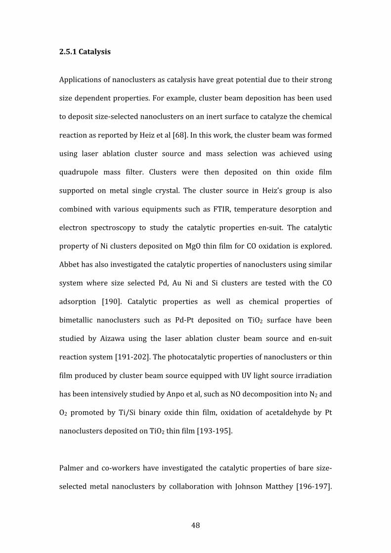
48
2.5.1 Catalysis
Applications of nanoclusters as catalysis have great potential due to their strong
size dependent properties. For example, cluster beam deposition has been used
to deposit size-‐selected nanoclusters on an inert surface to catalyze the chemical
reaction as reported by Heiz et al [68]. In this work, the cluster beam was formed
using laser ablation cluster source and mass selection was achieved using
quadrupole mass filter. Clusters were then deposited on thin oxide film
supported on metal single crystal. The cluster source in Heiz’s group is also
combined with various equipments such as FTIR, temperature desorption and
electron spectroscopy to study the catalytic properties en-‐suit. The catalytic
property of Ni clusters deposited on MgO thin film for CO oxidation is explored.
Abbet has also investigated the catalytic properties of nanoclusters using similar
system where size selected Pd, Au Ni and Si clusters are tested with the CO
adsorption [190]. Catalytic properties as well as chemical properties of
bimetallic nanoclusters such as Pd-‐Pt deposited on TiO2 surface have been
studied by Aizawa using the laser ablation cluster beam source and en-‐suit
reaction system [191-‐202]. The photocatalytic properties of nanoclusters or thin
film produced by cluster beam source equipped with UV light source irradiation
has been intensively studied by Anpo et al, such as NO decomposition into N2 and
O2 promoted by Ti/Si binary oxide thin film, oxidation of acetaldehyde by Pt
nanoclusters deposited on TiO2 thin film [193-‐195].
Palmer and co-‐workers have investigated the catalytic properties of bare size-‐
selected metal nanoclusters by collaboration with Johnson Matthey [196-‐197].
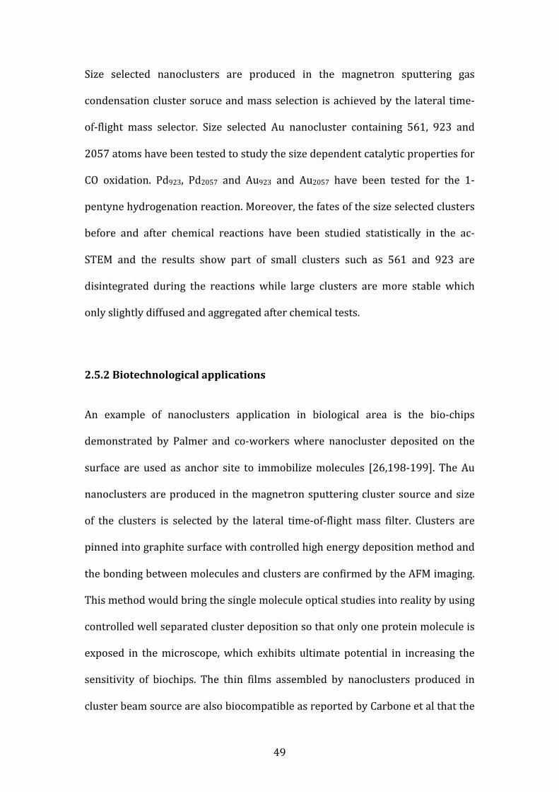
49
Size selected nanoclusters are produced in the magnetron sputtering gas
condensation cluster soruce and mass selection is achieved by the lateral time-‐
of-‐flight mass selector. Size selected Au nanocluster containing 561, 923 and
2057 atoms have been tested to study the size dependent catalytic properties for
CO oxidation. Pd923, Pd2057 and Au923 and Au2057 have been tested for the 1-‐
pentyne hydrogenation reaction. Moreover, the fates of the size selected clusters
before and after chemical reactions have been studied statistically in the ac-‐
STEM and the results show part of small clusters such as 561 and 923 are
disintegrated during the reactions while large clusters are more stable which
only slightly diffused and aggregated after chemical tests.
2.5.2 Biotechnological applications
An example of nanoclusters application in biological area is the bio-‐chips
demonstrated by Palmer and co-‐workers where nanocluster deposited on the
surface are used as anchor site to immobilize molecules [26,198-‐199]. The Au
nanoclusters are produced in the magnetron sputtering cluster source and size
of the clusters is selected by the lateral time-‐of-‐flight mass filter. Clusters are
pinned into graphite surface with controlled high energy deposition method and
the bonding between molecules and clusters are confirmed by the AFM imaging.
This method would bring the single molecule optical studies into reality by using
controlled well separated cluster deposition so that only one protein molecule is
exposed in the microscope, which exhibits ultimate potential in increasing the
sensitivity of biochips. The thin films assembled by nanoclusters produced in
cluster beam source are also biocompatible as reported by Carbone et al that the
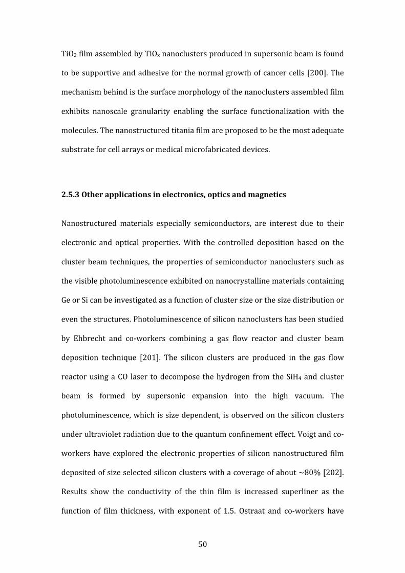
50
TiO2 film assembled by TiOx nanoclusters produced in supersonic beam is found
to be supportive and adhesive for the normal growth of cancer cells [200]. The
mechanism behind is the surface morphology of the nanoclusters assembled film
exhibits nanoscale granularity enabling the surface functionalization with the
molecules. The nanostructured titania film are proposed to be the most adequate
substrate for cell arrays or medical microfabricated devices.
2.5.3 Other applications in electronics, optics and magnetics
Nanostructured materials especially semiconductors, are interest due to their
electronic and optical properties. With the controlled deposition based on the
cluster beam techniques, the properties of semiconductor nanoclusters such as
the visible photoluminescence exhibited on nanocrystalline materials containing
Ge or Si can be investigated as a function of cluster size or the size distribution or
even the structures. Photoluminescence of silicon nanoclusters has been studied
by Ehbrecht and co-‐workers combining a gas flow reactor and cluster beam
deposition technique [201]. The silicon clusters are produced in the gas flow
reactor using a CO laser to decompose the hydrogen from the SiH4 and cluster
beam is formed by supersonic expansion into the high vacuum. The
photoluminescence, which is size dependent, is observed on the silicon clusters
under ultraviolet radiation due to the quantum confinement effect. Voigt and co-‐
workers have explored the electronic properties of silicon nanostructured film
deposited of size selected silicon clusters with a coverage of about ~80% [202].
Results show the conductivity of the thin film is increased superliner as the
function of film thickness, with exponent of 1.5. Ostraat and co-‐workers have
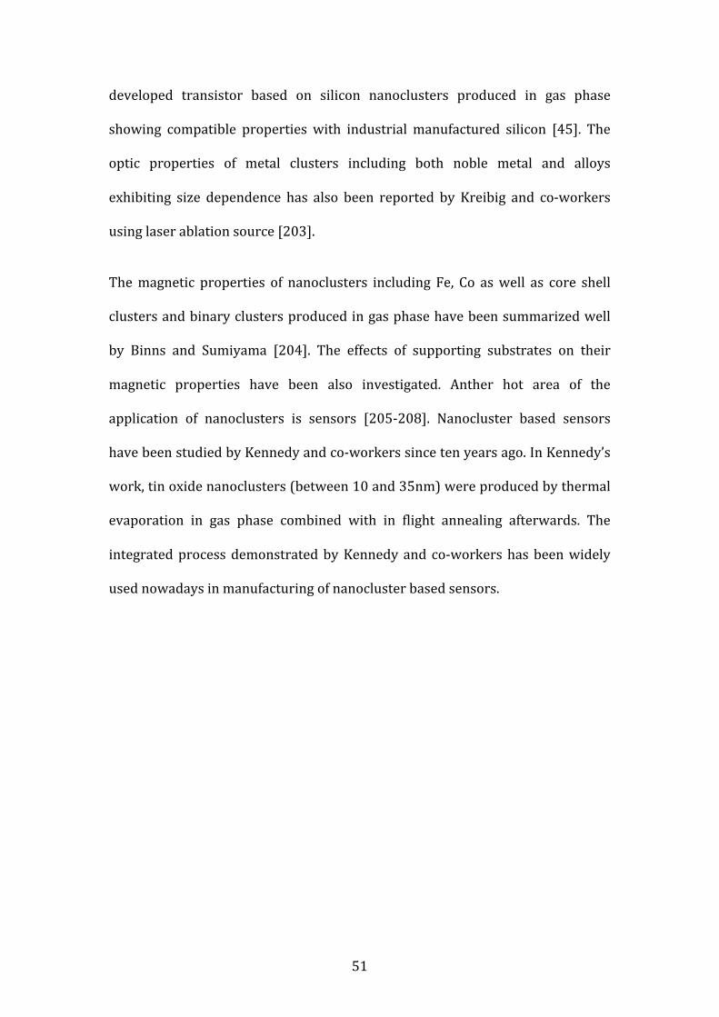
51
developed transistor based on silicon nanoclusters produced in gas phase
showing compatible properties with industrial manufactured silicon [45]. The
optic properties of metal clusters including both noble metal and alloys
exhibiting size dependence has also been reported by Kreibig and co-‐workers
using laser ablation source [203].
The magnetic properties of nanoclusters including Fe, Co as well as core shell
clusters and binary clusters produced in gas phase have been summarized well
by Binns and Sumiyama [204]. The effects of supporting substrates on their
magnetic properties have been also investigated. Anther hot area of the
application of nanoclusters is sensors [205-‐208]. Nanocluster based sensors
have been studied by Kennedy and co-‐workers since ten years ago. In Kennedy’s
work, tin oxide nanoclusters (between 10 and 35nm) were produced by thermal
evaporation in gas phase combined with in flight annealing afterwards. The
integrated process demonstrated by Kennedy and co-‐workers has been widely
used nowadays in manufacturing of nanocluster based sensors.
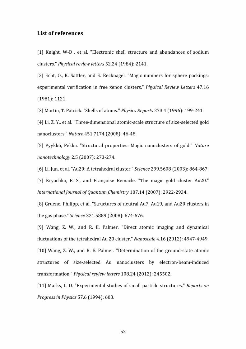
52
List of references
[1] Knight, W-‐D_, et al. "Electronic shell structure and abundances of sodium
clusters." Physical review letters 52.24 (1984): 2141.
[2] Echt, O., K. Sattler, and E. Recknagel. "Magic numbers for sphere packings:
experimental verification in free xenon clusters." Physical Review Letters 47.16
(1981): 1121.
[3] Martin, T. Patrick. "Shells of atoms." Physics Reports 273.4 (1996): 199-‐241.
[4] Li, Z. Y., et al. "Three-‐dimensional atomic-‐scale structure of size-‐selected gold
nanoclusters." Nature 451.7174 (2008): 46-‐48.
[5] Pyykkö, Pekka. "Structural properties: Magic nanoclusters of gold." Nature
nanotechnology 2.5 (2007): 273-‐274.
[6] Li, Jun, et al. "Au20: A tetrahedral cluster." Science 299.5608 (2003): 864-‐867.
[7] Kryachko, E. S., and Françoise Remacle. "The magic gold cluster Au20."
International Journal of Quantum Chemistry 107.14 (2007): 2922-‐2934.
[8] Gruene, Philipp, et al. "Structures of neutral Au7, Au19, and Au20 clusters in
the gas phase." Science 321.5889 (2008): 674-‐676.
[9] Wang, Z. W., and R. E. Palmer. "Direct atomic imaging and dynamical
fluctuations of the tetrahedral Au 20 cluster." Nanoscale 4.16 (2012): 4947-‐4949.
[10] Wang, Z. W., and R. E. Palmer. "Determination of the ground-‐state atomic
structures of size-‐selected Au nanoclusters by electron-‐beam-‐induced
transformation." Physical review letters 108.24 (2012): 245502.
[11] Marks, L. D. "Experimental studies of small particle structures." Reports on
Progress in Physics 57.6 (1994): 603.
53
[12] Jian, Nan, et al. "Hybrid atomic structure of the Schmid cluster Au 55 (PPh 3)
12 Cl 6 resolved by aberration-‐corrected STEM." Nanoscale 7.3 (2015): 885-‐888.
[13] Valden, M., X. Lai, and Dz W. Goodman. "Onset of catalytic activity of gold
clusters on titania with the appearance of nonmetallic properties." Science
281.5383 (1998): 1647-‐1650.
[14] Reetz, Manfred T., et al. "Visualization of surfactants on nanostructured
palladium clusters by a combination of STM and high-‐resolution TEM." Science
267.5196 (1995): 367.
[15] Morales, Alfredo M., and Charles M. Lieber. "A laser ablation method for the
synthesis of crystalline semiconductor nanowires." Science 279.5348 (1998):
208-‐211.
[16] Billas, Isabelle ML, A. Chatelain, and Walt A. de Heer. "Magnetism from the
atom to the bulk in iron, cobalt, and nickel clusters." Science 265.5179 (1994):
1682-‐1684.
[17] Rossi, Giulia, et al. "Magic polyicosahedral core-‐shell clusters." Physical
review letters 93.10 (2004): 105503.
[18] Lauritsen, Jeppe V., et al. "Size-‐dependent structure of MoS2 nanocrystals."
Nature nanotechnology 2.1 (2007): 53-‐58.
[19] Häkkinen, Hannu, et al. "Structural, electronic, and impurity-‐doping effects
in nanoscale chemistry: supported gold nanoclusters." Angewandte Chemie
International Edition 42.11 (2003): 1297-‐1300.
[20] Daniel, Marie-‐Christine, and Didier Astruc. "Gold nanoparticles: assembly,
supramolecular chemistry, quantum-‐size-‐related properties, and applications
toward biology, catalysis, and nanotechnology." Chemical reviews 104.1 (2004):
293-‐346.
54
[21] Xu, Z., et al. "Size-‐dependent catalytic activity of supported metal clusters."
(1994): 346-‐348.
[22] Heiz, U., et al. "Catalytic oxidation of carbon monoxide on monodispersed
platinum clusters: each atom counts." Journal of the American Chemical Society
121.13 (1999): 3214-‐3217.
[23] Lee, Sungsik, et al. "CO oxidation on Au n/TiO2 catalysts produced by size-‐
selected cluster deposition." Journal of the American Chemical Society 126.18
(2004): 5682-‐5683.
[24] Vajda, Stefan, et al. "Subnanometre platinum clusters as highly active and
selective catalysts for the oxidative dehydrogenation of propane." Nature
materials 8.3 (2009): 213-‐216.
[25] Tada, Tetsuya, et al. "Formation of 10 nm Si structures using size-‐selected
metal clusters." Journal of Physics D: Applied Physics 31.7 (1998): L21.
[26] Palmer, Richard E., and Carl Leung. "Immobilisation of proteins by atomic
clusters on surfaces." TRENDS in Biotechnology 25.2 (2007): 48-‐55.
[27] Leung, Carl, et al. "Immobilization of Protein Molecules by Size-‐Selected
Metal Clusters on Surfaces." Advanced Materials 16.3 (2004): 223-‐226.
[28] Wenseleers, Wim, et al. "Five orders-‐of-‐magnitude enhancement of two-‐
photon absorption for dyes on silver nanoparticle fractal clusters." The Journal of
Physical Chemistry B 106.27 (2002): 6853-‐6863.
[29] Stenzel, O., et al. "Enhancement of the photovoltaic conversion efficiency of
copper phthalocyanine thin film devices by incorporation of metal clusters."
Solar energy materials and solar cells 37.3 (1995): 337-‐348.
55
[30] Rand, Barry P., Peter Peumans, and Stephen R. Forrest. "Long-‐range
absorption enhancement in organic tandem thin-‐film solar cells containing silver
nanoclusters." Journal of Applied Physics 96.12 (2004): 7519-‐7526.
[31] Zhao, Linlin, Lasse Jensen, and George C. Schatz. "Pyridine-‐Ag20 cluster: a
model system for studying surface-‐enhanced Raman scattering." Journal of the
American chemical society 128.9 (2006): 2911-‐2919.
[32] Nie, Shuming, and Steven R. Emory. "Probing single molecules and single
nanoparticles by surface-‐enhanced Raman scattering." science 275.5303 (1997):
1102-‐1106.
[33] Dietz, Thomas G., et al. "Laser production of supersonic metal cluster
beams." The Journal of Chemical Physics 74.11 (1981): 6511-‐6512.
[34] De Heer, Walt A. "The physics of simple metal clusters: experimental aspects
and simple models." Reviews of Modern Physics 65.3 (1993): 611.
[35] Stark, Wendelin J., and Sotiris E. Pratsinis. "Aerosol flame reactors for
manufacture of nanoparticles." Powder Technology 126.2 (2002): 103-‐108.
[36] Wegner, K., et al. "Cluster beam deposition: a tool for nanoscale science and
technology." Journal of Physics D: Applied Physics 39.22 (2006): R439.
[37] Lockwood, David J. "Nanostructure Science and Technology."
[38] Wegner, Karsten, and Sotiris E. Pratsinis. "Scale-‐up of nanoparticle synthesis
in diffusion flame reactors." Chemical Engineering Science 58.20 (2003): 4581-‐
4589.
[39] Kammler, Hendrik K., Lutz Mädler, and Sotiris E. Pratsinis. "Flame synthesis
of nanoparticles." Chemical engineering & technology 24.6 (2001): 583-‐596.
56
[40] Singh, Yogendra, et al. "Approaches to increasing yield in
evaporation/condensation nanoparticle generation." Journal of Aerosol Science
33.9 (2002): 1309-‐1325.
[41] Wegner, Karsten, and Sotiris E. Pratsinis. "Nozzle-‐quenching process for
controlled flame synthesis of titania nanoparticles." AIChE Journal 49.7 (2003):
1667-‐1675.
[42] Nakaso, Koichi, et al. "Evaluation of the change in the morphology of gold
nanoparticles during sintering." Journal of Aerosol Science 33.7 (2002): 1061-‐
1074.
[43] Nanda, K. K., et al. "Band-‐gap tuning of PbS nanoparticles by in-‐flight
sintering of size classified aerosols." Journal of applied physics 91.4 (2002): 2315-‐
2321.
[44] Karlsson, Martin NA, et al. "Size-‐and composition-‐controlled Au–Ga aerosol
nanoparticles." Aerosol science and technology 38.9 (2004): 948-‐954.
[45] Ostraat, Michele L., et al. "Ultraclean two-‐stage aerosol reactor for
production of oxide-‐passivated silicon nanoparticles for novel memory devices."
Journal of The Electrochemical Society 148.5 (2001): G265-‐G270.
[46] Milani, Paolo, and Salvatore Iannotta. Cluster beam synthesis of
nanostructured materials. Springer Science & Business Media, 2012.
[47] Milani, P., et al. "Cluster beam synthesis of nanostructured thin films."
Journal of Vacuum Science & Technology A 19.4 (2001): 2025-‐2033.
[48] Mazza, T., et al. "Libraries of cluster-‐assembled titania films for chemical
sensing." Applied Physics Letters 87.10 (2005): 103108.
[49] Granqvist, C. G., and R. A. Buhrman. "Ultrafine metal particles." Journal of
Applied Physics 47.5 (1976): 2200-‐2219.
57
[50] Haberland, Hellmut, et al. "Thin films from energetic cluster impact: a
feasibility study." Journal of Vacuum Science & Technology A 10.5 (1992): 3266-‐
3271.
[51] Hihara, Takehiko, and Kenji Sumiyama. "Formation and size control of a Ni
cluster by plasma gas condensation." Journal of applied physics 84.9 (1998):
5270-‐5276.
[52] Yamamuro, S., Kenji Sumiyama, and K. Suzuki. "Monodispersed Cr cluster
formation by plasma-‐gas-‐condensation." Journal of applied physics 85.1 (1999):
483-‐489.
[53] Sumiyama, Kenji, et al. "Structure and magnetic properties of Co/CoO and
Co/Si core–shell cluster assemblies prepared via gas-‐phase." Science and
Technology of Advanced Materials 6.1 (2005): 18-‐26.
[54] Goldby, Ian Michael. Dynamics of molecules and clusters at surfaces. Diss.
University of Cambridge, 1996.
[55] Uyeda, Ryozi. "Studies of ultrafine particles in Japan: crystallography.
Methods of preparation and technological applications." Progress in Materials
Science 35.1 (1991): 1-‐96.
[56] Hihara, Takehiko, and Kenji Sumiyama. "Formation and size control of a Ni
cluster by plasma gas condensation." Journal of applied physics 84.9 (1998):
5270-‐5276.
[57] Lehtinen, Kari EJ, and Michael R. Zachariah. "Self-‐preserving theory for the
volume distribution of particles undergoing Brownian coagulation." Journal of
Colloid and Interface Science 242.2 (2001): 314-‐318.
[58] Gatz, P., and O. F. Hagena. "Cluster beams for metallization of
microstructured surfaces." Applied surface science 91.1 (1995): 169-‐174.
58
[59] Ross, K. J., and B. Sonntag. "High temperature metal atom beam sources."
Review of scientific instruments 66.9 (1995): 4409-‐4433.
[60] Ross, K. J., and B. Sonntag. "High temperature metal atom beam sources."
Review of scientific instruments 66.9 (1995): 4409-‐4433.
[61] Bewig, L., et al. "Seeded supersonic alkali cluster beam source with refilling
system." Review of scientific instruments 63.8 (1992): 3936-‐3938.
[62] Binns, C. "Nanoclusters deposited on surfaces." Surface science reports 44.1
(2001): 1-‐49.
[63] Dietz, Thomas G., et al. "Laser production of supersonic metal cluster
beams." The Journal of Chemical Physics 74.11 (1981): 6511-‐6512.
[64] Duncan, Michael A. "Invited Review Article: Laser vaporization cluster
sourcesa)." Review of Scientific Instruments 83.4 (2012): 041101.
[65] Maruyama, Shigeo, Lila R. Anderson, and Richard E. Smalley. "Direct
injection supersonic cluster beam source for FT-‐ICR studies of clusters." Review
of scientific instruments 61.12 (1990): 3686-‐3693.
[66] Milani, Paolo. "Improved pulsed laser vaporization source for production of
intense beams of neutral and ionized clusters." Review of scientific instruments
61.7 (1990): 1835-‐1838.
[67] Geusic, M. E., et al. "Surface reactions of metal clusters I: The fast flow
cluster reactor." Review of Scientific Instruments 56.11 (1985): 2123-‐2130.
[68] Heiz, U., et al. "Chemical reactivity of size-‐selected supported clusters: An
experimental setup." Review of scientific instruments 68.5 (1997): 1986-‐1994.
[69] Woenckhaus, J., and J. A. Becker. "A fast pressure monitor for pulsed laser
vaporization cluster sources." Review of scientific instruments 65.6 (1994): 2019-‐
2022.
59
[70] Bansmann, Joachim, et al. "Magnetic and structural properties of isolated
and assembled clusters." Surface Science Reports 56.6 (2005): 189-‐275.
[71] Haberland, H., M. Karrais, and M. Mall. "A new type of cluster and cluster ion
source." Zeitschrift für Physik D Atoms, Molecules and Clusters 20.1 (1991): 413-‐
415.
[72] Raizer, Yuri P., and John E. Allen. Gas discharge physics. Vol. 2. Berlin:
Springer, 1997.
[73] Haberland, Hellmut, et al. "Thin films from energetic cluster impact: a
feasibility study." Journal of Vacuum Science & Technology A 10.5 (1992): 3266-‐
3271.
[74] Pratontep, S., et al. "Size-‐selected cluster beam source based on radio
frequency magnetron plasma sputtering and gas condensation." Review of
scientific instruments 76.4 (2005): 045103.
[75] Smith, Roger. Atomic and ion collisions in solids and at surfaces: theory,
simulation and applications. Cambridge University Press, 2005.
[76] Olynick, D. L., J. M. Gibson, and R. S. Averback. "Impurity-‐suppressed
sintering in copper nanophase materials." Philosophical Magazine A 77.5 (1998):
1205-‐1221.
[77] Soler, J. M., et al. "Microcluster growth: transition from successive monomer
addition to coagulation." Physical Review Letters 49.25 (1982): 1857.
[78] Hihara, Takehiko, and Kenji Sumiyama. "Formation and size control of a Ni
cluster by plasma gas condensation." Journal of applied physics 84.9 (1998):
5270-‐5276.
60
[79] Barborini, E., P. Piseri, and P. Milani. "A pulsed microplasma source of high
intensity supersonic carbon cluster beams." Journal of Physics D: Applied Physics
32.21 (1999): L105.
[80] Tafreshi, H. Vahedi, et al. "The role of gas dynamics in operation conditions
of a pulsed microplasma cluster source for nanostructured thin films
deposition." Journal of nanoscience and nanotechnology 6.4 (2006): 1140-‐1149.
[81] Bongiorno, G., et al. "Nanocrystalline metal/carbon composites produced by
supersonic cluster beam deposition." Journal of nanoscience and nanotechnology
5.7 (2005): 1072-‐1080.
[82] Ganteför, Gerd, et al. "Pure metal and metal-‐doped rare-‐gas clusters grown
in a pulsed ARC cluster ion source." Chemical Physics Letters 165.4 (1990): 293-‐
296.
[83] Ganteför, Gerd, et al. "Pure metal and metal-‐doped rare-‐gas clusters grown
in a pulsed ARC cluster ion source." Chemical Physics Letters 165.4 (1990): 293-‐
296.
[84] Siekmann, H. R., et al. "VUV-‐photoelectron spectroscopy on lead clusters
deposited from the pulsed arc cluster ion source (PACIS)." Zeitschrift für Physik B
Condensed Matter 90.2 (1993): 201-‐206.
[85] Cha, Chia-‐Yen, Gerd Ganteför, and Wolfgang Eberhardt. "New experimental
setup for photoelectron spectroscopy on cluster anions." Review of scientific
instruments 63.12 (1992): 5661-‐5666.
[86] Mohanty, U. S. "Electrodeposition: a versatile and inexpensive tool for the
synthesis of nanoparticles, nanorods, nanowires, and nanoclusters of metals."
Journal of applied electrochemistry 41.3 (2011): 257-‐270.
61
[87] Niu, Wenxin, and Guobao Xu. "Crystallographic control of noble metal
nanocrystals." Nano Today 6.3 (2011): 265-‐285.
[88] Moriarty, Philip. "Nanostructured materials." Reports on Progress in Physics
64.3 (2001): 297.
[89] Faraday, Michael. "The Bakerian lecture: experimental relations of gold (and
other metals) to light." Philosophical Transactions of the Royal Society of London
147 (1857): 145-‐181.
[90] Xia, Younan, et al. "Shape-‐Controlled Synthesis of Metal Nanocrystals:
Simple Chemistry Meets Complex Physics?." Angewandte Chemie International
Edition 48.1 (2009): 60-‐103.
[91] Fennell, John, et al. "A selective blocking method to control the overgrowth
of Pt on Au nanorods." Journal of the American Chemical Society 135.17 (2013):
6554-‐6561.
[92] URL http://www.nobelprize.org/nobel_prizes/physics/laureates
[93] Williams, David B., and C. Barry Carter. The transmission electron
microscope. Springer Us, 1996.
[94] Nellist, P. D., and S. J. Pennycook. "Incoherent imaging using dynamically
scattered coherent electrons." Ultramicroscope 78.1 (1999): 111-‐124.
[95] Scherzer, O_. "über einige Fehler von Elektronenlinsen." Zeitschrift für
Physik 101.9-‐10 (1936): 593-‐603.
[96] Scherzer, O. "Spharische und chromatische korrektur von elektronen-‐
linsen." Optik 2 (1947): 114-‐132.
[97] Lupini, Andrew R., et al. "Characterizing the two-‐and three-‐dimensional
resolution of an improved aberration-‐corrected STEM." Microscope and
Microanalysis 15.05 (2009): 441-‐453.
62
[98] Haider, Maximilian, et al. "Electron microscope image enhanced." Nature
392 (1998): 768-‐769.
[99] Borisevich, Albina Y., Andrew R. Lupini, and Stephen J. Pennycook. "Depth
sectioning with the aberration-‐corrected scanning transmission electron
microscope." Proceedings of the National Academy of Sciences of the United
States of America 103.9 (2006): 3044-‐3048.
[100] Haider, M., S. Uhlemann, and J. Zach. "Upper limits for the residual
aberrations of a high-‐resolution aberration-‐corrected STEM." Ultramicroscope
81.3 (2000): 163-‐175.
[101] Rose, H. H. "Optics of high-‐performance electron microscopes." Science and
Technology of Advanced Materials 9.1 (2008): 014107.
[102] Haider, Max, et al. "A spherical-‐aberration-‐corrected 200kV transmission
electron microscope." Ultramicroscope 75.1 (1998): 53-‐60.
[103] Klenov, Dmitri O., and Susanne Stemmer. "Contributions to the contrast in
experimental high-‐angle annular dark-‐field images." Ultramicroscope 106.10
(2006): 889-‐901.
[104] Wang, Z. W., et al. "Quantitative Z-‐contrast imaging in the scanning
transmission electron microscope with size-‐selected clusters." Physical Review B
84.7 (2011): 073408.
[105] Nellist, P. D., and S. J. Pennycook. "The Principles and Interpretations of
Annular Dark-‐Field Z-‐Contrast Imaging." Advances in Imaging and Electron
Physics 113 (2000): 148-‐204.
[106] Jesson, D. E., and S. J. Pennycook. "Incoherent imaging of crystals using
thermally scattered electrons." Proceedings of the Royal Society of London A:
63
Mathematical, Physical and Engineering Sciences. Vol. 449. No. 1936. The Royal
Society, 1995.
[107] Mackay, A. L. "A dense non-‐crystallographic packing of equal spheres."
Acta Crystallographica 15.9 (1962): 916-‐918.
[108] Echt, O., K. Sattler, and E. Recknagel. "Magic numbers for sphere packings:
experimental verification in free xenon clusters." Physical Review Letters 47.16
(1981): 1121.
[109] Honeycutt, J. Dana, and Hans C. Andersen. "Molecular dynamics study of
melting and freezing of small Lennard-‐Jones clusters." Journal of Physical
Chemistry 91.19 (1987): 4950-‐4963.
[110] Martin, T. P., et al. "Shell structure of clusters." The Journal of Physical
Chemistry 95.17 (1991): 6421-‐6429.
[111] Martin, T. Patrick. "Shells of atoms." Physics Reports 273.4 (1996): 199-‐
241.
[112] Ino, Shozo. "Stability of multiply-‐twinned particles." Journal of the Physical
Society of Japan 27.4 (1969): 941-‐953.
[113] Raoult, B., et al. "Comparison between icosahedral, decahedral and
crystalline Lennard-‐Jones models containing 500 to 6000 atoms." Philosophical
Magazine B 60.6 (1989): 881-‐906.
[114] Marks, L. D. "Surface structure and energetics of multiply twinned
particles." Philosophical Magazine A 49.1 (1984): 81-‐93.
[115] Marks, L. D. "Modified Wulff constructions for twinned particles." Journal
of Crystal Growth 61.3 (1983): 556-‐566.
64
[116] Baletto, Francesca, and Riccardo Ferrando. "Structural properties of
nanoclusters: Energetic, thermodynamic, and kinetic effects." Reviews of modern
physics 77.1 (2005): 371.
[117] Mackay, A. L. "A dense non-‐crystallographic packing of equal spheres."
Acta Crystallographica 15.9 (1962): 916-‐918.
[118] Kuo, K. H. "Mackay, anti-‐Mackay, double-‐Mackay, pseudo-‐Mackay, and
related icosahedral shell clusters." Structural Chemistry 13.3-‐4 (2002): 221-‐230.
[119] Mottet, C., et al. "Modeling free and supported metallic nanoclusters:
structure and dynamics." Phase Transitions 77.1-‐2 (2004): 101-‐113.
[120] Nam, H-‐S., et al. "Formation of an icosahedral structure during the freezing
of gold nanoclusters: surface-‐induced mechanism." Physical review letters 89.27
(2002): 275502.
[121] Chushak, Yaroslav G., and Lawrence S. Bartell. "Melting and freezing of gold
nanoclusters." The Journal of Physical Chemistry B 105.47 (2001): 11605-‐11614.
[122] Cleveland, Charles L., W. D. Luedtke, and Uzi Landman. "Melting of gold
clusters: Icosahedral precursors." Physical review letters 81.10 (1998): 2036.
[123] Baletto, F., C. Mottet, and R. Ferrando. "Microscopic mechanisms of the
growth of metastable silver icosahedra." Physical Review B 63.15 (2001):
155408.
[124] Barnard, A. S., et al. "Ideality versus reality: Emergence of the Chui
icosahedron." The Journal of Physical Chemistry C 112.38 (2008): 14848-‐14852.
[125] Chui, Yu Hang, et al. "Topological characterization of crystallization of gold
nanoclusters." The Journal of chemical physics 125.11 (2006): 114703.
65
[126] Chui, Yu Hang, et al. "Molecular dynamics investigation of the structural
and thermodynamic properties of gold nanoclusters of different morphologies."
Physical Review B 75.3 (2007): 033404.
[127] Cleveland, Charles L., and Uzi Landman. "The energetics and structure of
nickel clusters: size dependence." The Journal of chemical physics 94.11 (1991):
7376-‐7396.
[128] Ascencio, J. A., et al. "Structure determination of small particles by HREM
imaging: theory and experiment." Surface Science 396.1 (1998): 349-‐368.
[129] Baletto, F., et al. "Crossover among structural motifs in transition and
noble-‐metal clusters." The Journal of chemical physics 116.9 (2002): 3856-‐3863.
[130] Germer Jr, Henry A. "Solvent interaction within the Hartree-‐Fock SCF
molecular orbital formalism." Theoretica chimica acta 34.2 (1974): 145-‐155.
[131] Ho, Kai-‐Ming, et al. "Structures of medium-‐sized silicon clusters." Nature
392.6676 (1998): 582-‐585.
[132] Barreteau, C., et al. "spd tight-‐binding model of magnetism in transition
metals: Application to Rh and Pd clusters and slabs." Physical Review B 61.11
(2000): 7781.
[133] Ferrando, Riccardo, Julius Jellinek, and Roy L. Johnston. "Nanoalloys: from
theory to applications of alloy clusters and nanoparticles." Chemical reviews
108.3 (2008): 845-‐910.
[134] Grochola, Gregory, Salvy P. Russo, and Ian K. Snook. "On morphologies of
gold nanoparticles grown from molecular dynamics simulation." The Journal of
chemical physics 126.16 (2007): 164707.
66
[135] Feigl, Christopher, et al. "A theoretical study of size and temperature
dependent morphology transformations in gold nanoparticles." Chemical Physics
Letters 474.1 (2009): 115-‐118.
[136] Desgranges, Caroline, and Jerome Delhommelle. "Molecular simulation of
the nucleation and growth of gold nanoparticles." The Journal of Physical
Chemistry C 113.9 (2009): 3607-‐3611.
[137] Barnard, Amanda S. "Direct comparison of kinetic and thermodynamic
influences on gold nanomorphology." Accounts of chemical research 45.10
(2012): 1688-‐1697.
[138] Baletto, F., C. Mottet, and R. Ferrando. "Reentrant morphology transition in
the growth of free silver nanoclusters." Physical review letters 84.24 (2000):
5544.
[139] Grochola, G., et al. "Exploring the effects of different immersion
environments on the growth of gold nanostructures." Molecular Simulation 32.15
(2006): 1255-‐1260.
[140] Barnard, Amanda S., et al. "Nanogold: a quantitative phase map." ACS nano
3.6 (2009): 1431-‐1436.
[141] Kuo, Chin-‐Lung, and Paulette Clancy. "Melting and freezing characteristics
and structural properties of supported and unsupported gold nanoclusters." The
Journal of Physical Chemistry B 109.28 (2005): 13743-‐13754.
[142] Wang, Yanting, S. Teitel, and Christoph Dellago. "Melting of icosahedral
gold nanoclusters from molecular dynamics simulations." The Journal of chemical
physics 122.21 (2005): 214722.
[143] Chen, Fuyi, Z. Y. Li, and Roy L. Johnston. "Surface reconstruction precursor
to melting in Au309 clusters." AIP Advances 1.3 (2011): 032105.
67
[144] Doye, J. P. K., and D. J. Wales. "Thermally-‐induced surface reconstructions
of Mackay icosahedra." Zeitschrift für Physik D Atoms, Molecules and Clusters 40.1
(1997): 466-‐468.
[145] Ercolessi, Furio, Wanda Andreoni, and Erio Tosatti. "Melting of small gold
particles: Mechanism and size effects." Physical Review Letters 66.7 (1991): 911.
[146] Schebarchov, D., and S. C. Hendy. "Thermal instability of decahedral
structures in platinum nanoparticles." The European Physical Journal D 43.1-‐3
(2007): 11-‐14.
[147] Schebarchov, D., S. C. Hendy, and W. Polak. "Molecular dynamics study of
the melting of a supported 887-‐atom Pd decahedron." Journal of Physics:
Condensed Matter 21.14 (2009): 144204.
[148] Chushak, Y., and Lawrence S. Bartell. "Molecular dynamics simulations of
the freezing of gold nanoparticles." The European Physical Journal D-‐Atomic,
Molecular, Optical and Plasma Physics 16.1 (2001): 43-‐46.
[149] Opletal, G., et al. "Elucidation of surface driven crystallization of
icosahedral clusters." Chemical Physics Letters 482.4 (2009): 281-‐286.
[150] Delogu, F. "A numerical study of the freezing behavior of an unsupported
nanometer-‐sized Au droplet." Nanotechnology 18.48 (2007): 485710.
[151] Chui, Yu Hang, Ian K. Snook, and Salvy P. Russo. "Visualization and analysis
of structural ordering during crystallization of a gold nanoparticle." Physical
Review B 76.19 (2007): 195427.
[152] Schwoebel, R. L. "Condensation of gold on gold single crystals." Surface
Science 2 (1964): 356-‐366.
68
[153] Ino, Shozo. "Epitaxial growth of metals on rocksalt faces cleaved in
vacuum. II. Orientation and structure of gold particles formed in ultrahigh
vacuum." Journal of the Physical Society of Japan 21.2 (1966): 346-‐362.
[154] Ino, Shozo, and Shiro Ogawa. "Multiply twinned particles at earlier stages
of gold film formation on alkalihalide crystals." Journal of the Physical Society of
Japan 22.6 (1967): 1365-‐1374.
[155] Allpress, J. G., and J. V. Sanders. "The structure and orientation of crystals
in deposits of metals on mica." Surface Science 7.1 (1967): 1-‐25.
[156] Komoda, Tsutomu. "Study on the structure of evaporated gold particles by
means of a high resolution electron microscope." Japanese Journal of Applied
Physics 7.1 (1968): 27.
[157] Ogawa, Shiro, and Shozo Ino. "Formation of Multiply-‐Twinned Particles in
the Nucleation Stage of Film Growth." Journal of Vacuum Science & Technology
6.4 (1969): 527-‐534.
[158] Ogawa, Shiro, and Shozo Ino. "Formation of multiply-‐twinned particles on
alkali halide crystals by vacuum evaporation and their structures." Journal of
Crystal Growth 13 (1972): 48-‐56.
[159] Wayman, C. M., and T. P. Darby. "Nucleation and growth of gold films on
graphite: II. The effect of substrate temperature." Journal of Crystal Growth 28.1
(1975): 53-‐67.
[160] Gillet, M. "Structure of small metallic particles." Surface Science 67.1
(1977): 139-‐157.
[161] Heinemann, K., et al. "The structure of small, vapor-‐deposited particles: I.
Experimental study of single crystals and particles with pentagonal profiles."
Journal of Crystal Growth 47.2 (1979): 177-‐186.
69
[162] Renou, A., and M. Gillet. "Growth of Au, Pt and Pd particles in a flowing
argon system: Observations of decahedral and icosahedral structures." Surface
Science 106.1 (1981): 27-‐34.
[163] Hofmeister, H. "Habit and internal structure of multiply twinned gold
particles on silver bromide films." Thin Solid Films 116.1 (1984): 151-‐162.
[164] Pérez-‐Ramírez, J. G., et al. "On the equilibrium shape of multiple-‐twinned
particles." Superlattices and Microstructures 1.6 (1985): 485-‐487.
[165] Iijima, Sumio, and Toshinari Ichihashi. "Structural instability of ultrafine
particles of metals." Physical review letters 56.6 (1986): 616.
[166] Gao, Pei-‐Yu, et al. "The structure of small penta-‐twinned gold particles."
Zeitschrift für Physik D Atoms, Molecules and Clusters 12.1-‐4 (1989): 119-‐121.
[167] Jose-‐Yacaman, M., et al. "Decagonal and hexagonal structures in small gold
particles." Surface Science 237.1 (1990): 248-‐256.
[168] Uyeda, Natsu, Misao Nishino, and Eiji Suito. "Nucleus interaction and fine
structures of colloidal gold particles." Journal of Colloid and Interface Science 43.2
(1973): 264-‐276.
[169] Thölén, A. R. "Electron microscope investigation of small particles." Phase
Transitions: A Multinational Journal 24.1 (1990): 375-‐406.
[170] Lu, Da-‐ling, et al. "The shape and structure of gold particles grown at
different electrode potentials." Surface science 325.1 (1995): L397-‐L405.
[171] Nepijko, Sergej A., et al. "Multiply twinned particles beyond the
icosahedron." Journal of Crystal Growth 213.1 (2000): 129-‐134.
[172] Oku, Takeo, and Kenji Hiraga. "Atomic structures and stability of hexagonal
BN, diamond and Au multiply-‐twinned nanoparticles with five-‐fold symmetry."
Diamond and related materials 10.3 (2001): 1398-‐1403.
70
[173] Zanchet, D., B. D. Hall, and D. Ugarte. "Structure population in thiol-‐
passivated gold nanoparticles." The Journal of Physical Chemistry B 104.47
(2000): 11013-‐11018.
[174] Koga, K., and K-‐I. Sugawara. "Population statistics of gold nanoparticle
morphologies: direct determination by HREM observations." Surface science
529.1 (2003): 23-‐35.
[175] Mohr, Christian, Herbert Hofmeister, and Peter Claus. "The influence of
real structure of gold catalysts in the partial hydrogenation of acrolein." Journal
of Catalysis 213.1 (2003): 86-‐94.
[176] Hormozi Nezhad, Mohammad R., et al. "Synthesis and patterning of gold
nanostructures on InP and GaAs via galvanic displacement." Small 1.11 (2005):
1076-‐1081.
[177] Jiang, Peng, et al. "Poly (vinyl pyrrolidone)-‐capped five-‐fold twinned gold
particles with sizes from nanometres to micrometres." Nanotechnology 17.14
(2006): 3533.
[178] Esparza, R., et al. "Structural analysis and shape-‐dependent catalytic
activity of Au, Pt and Au/Pt nanoparticles." Matéria (Rio de Janeiro) 13.4 (2008):
579-‐586.
[179] Kwon, Kihyun, et al. "Controlled synthesis of icosahedral gold
nanoparticles and their surface-‐enhanced Raman scattering property." The
Journal of Physical Chemistry C 111.3 (2007): 1161-‐1165.
[180] Seo, Daeha, et al. "Shape adjustment between multiply twinned and single-‐
crystalline polyhedral gold nanocrystals: decahedra, icosahedra, and truncated
tetrahedra." The Journal of Physical Chemistry C 112.7 (2008): 2469-‐2475.
71
[181] Xu, Jun, et al. "Hydrothermal syntheses of gold nanocrystals: from
icosahedral to its truncated form." Advanced Functional Materials 18.2 (2008):
277-‐284.
[182] Wang, Y. Q., W. S. Liang, and C. Y. Geng. "Coalescence behavior of gold
nanoparticles." Nanoscale research letters 4.7 (2009): 684-‐688.
[183] Lim, Teck H., et al. "Real-‐time TEM and kinetic Monte Carlo studies of the
coalescence of decahedral gold nanoparticles." ACS nano 3.11 (2009): 3809-‐
3813.
[184] Zhang, Qingbo, et al. "Tuning the crystallinity of Au nanoparticles." Small
6.4 (2010): 523-‐527.
[185] Casillas, Gilberto, J. Jesús Velázquez-‐Salazar, and Miguel Jose-‐Yacaman. "A
New Mechanism of Stabilization of Large Decahedral Nanoparticles." The Journal
of Physical Chemistry C 116.15 (2012): 8844-‐8848.
[186] Young, N. P., et al. "Transformations of gold nanoparticles investigated
using variable temperature high-‐resolution transmission electron microscope."
Ultramicroscope 110.5 (2010): 506-‐516.
[187] Koga, Kenji, Tamio Ikeshoji, and Ko-‐ichi Sugawara. "Size-‐and temperature-‐
dependent structural transitions in gold nanoparticles." Physical review letters
92.11 (2004): 115507.
[188] Wells, Dawn M., et al. "Metastability of the atomic structures of size-‐
selected gold nanoparticles." Nanoscale 7.15 (2015): 6498-‐6503.
[189] Nalwa, Hari Singh. Encyclopedia of nanoscience and nanotechnology. CRC
Press, 2004.
72
[190] Abbet, Stéphane, et al. "Synthesis of monodispersed model catalysts using
softlanding cluster deposition." Pure and Applied Chemistry 74.9 (2002): 1527-‐
1535.
[191] Aires, FJ Cadete Santos, et al. "Scanning tunneling microscope study of
model catalysts obtained by cluster beam deposition of palladium onto highly
oriented pyrolitic graphite." Journal of Vacuum Science & Technology B 12.3
(1994): 1776-‐1779.
[192] Rousset, J. L., et al. "Characterization and reactivity of Pd–Pt bimetallic
supported catalysts obtained by laser vaporization of bulk alloy." Applied surface
science 164.1 (2000): 163-‐168.
[193] Takeuchi, Masato, et al. "Preparation of titanium-‐silicon binary oxide thin
film photocatalysts by an ionized cluster beam deposition method. Their
photocatalytic activity and photoinduced super-‐hydrophilicity." The Journal of
Physical Chemistry B 107.51 (2003): 14278-‐14282.
[194] Takeuchi, Masato, et al. "Effect of Pt loading on the photocatalytic
reactivity of titanium oxide thin films prepared by ion engineering techniques."
Research on chemical intermediates 29.6 (2003): 619-‐629.
[195] Zhou, Jinkai, et al. "Photocatalytic decomposition of formic acid under
visible light irradiation over V-‐ion-‐implanted TiO2 thin film photocatalysts
prepared on quartz substrate by ionized cluster beam (ICB) deposition method."
Catalysis letters 106.1-‐2 (2006): 67-‐70.
[196] Hu, Kuo-‐Juei, et al. "The effects of 1-‐pentyne hydrogenation on the atomic
structures of size-‐selected Au N and Pd N (N= 923 and 2057) nanoclusters."
Physical Chemistry Chemical Physics (2014).
73
[197] Malola, Sami, et al. "Au40 (SR) 24 cluster as a chiral dimer of 8-‐electron
superatoms: Structure and optical properties." Journal of the American Chemical
Society 134.48 (2012): 19560-‐19563.
[198] Collins, J. A., et al. "Clusters for biology: immobilization of proteins by size-‐
selected metal clusters." Applied surface science 226.1 (2004): 197-‐208.
[199] Palmer, R. E., S. Pratontep, and H-‐G. Boyen. "Nanostructured surfaces from
size-‐selected clusters." Nature Materials 2.7 (2003): 443-‐448.
[200] Carbone, Roberta, et al. "Biocompatibility of cluster-‐assembled
nanostructured TiO 2 with primary and cancer cells." Biomaterials 27.17 (2006):
3221-‐3229.
[201] Ehbrecht, M., et al. "Photoluminescence and resonant Raman spectra of
silicon films produced by size-‐selected cluster beam deposition." Physical Review
B 56.11 (1997): 6958.
[202] Voigt, F., et al. "Porous thin films grown from size-‐selected silicon
nanocrystals." Materials Science and Engineering: C 25.5 (2005): 584-‐589.
[203] Kreibig, Uwe, and Michael Vollmer. "Optical properties of metal clusters."
(1995).
[204] Binns, C., et al. "The behaviour of nanostructured magnetic materials
produced by depositing gas-‐phase nanoparticles." Journal of Physics D: Applied
Physics 38.22 (2005): R357.
[205] Qiu, Jiao-‐Ming, et al. "Nanocluster deposition for high density magnetic
recording tape media." Journal of applied physics 97.10 (2005): 10P704.
[206] Kennedy, M. K., et al. "Tailored nanoparticle films from monosized tin
oxide nanocrystals: particle synthesis, film formation, and size-‐dependent gas-‐
sensing properties." Journal of Applied Physics 93.1 (2003): 551-‐560.
74
[207] Mädler, L., et al. "Direct formation of highly porous gas-‐sensing films by in
situ thermophoretic deposition of flame-‐made Pt/SnO 2 nanoparticles." Sensors
and Actuators B: Chemical 114.1 (2006): 283-‐295.
[208] Kennedy, M. K., et al. "Effect of in-‐flight annealing and deposition method
on gas-‐sensitive SnO x films made from size-‐selected nanoparticles." Sensors and
Actuators B: Chemical 108.1 (2005): 62-‐69.
75
Chapter 3 Experimental apparatus
In this chapter, we introduce the two pre-‐existing apparatuses used in the works
presented in the thesis: the magnetron sputtering cluster source with time-‐of-‐
flight mass filter built by Birmingham Instruments (BI) and the aberration
corrected scanning transmission electron microscope (JEOL 2100F). The
magnetron sputtering cluster source with time-‐of-‐flight mass filter is one of the
few techniques available to carry out controlled deposition of size-‐selected
nanoclusters and is used for the cluster production work presented in Chapter 4.
The aberration corrected scanning transmission electron microscope is a
powerful tool with the potential to obtain abundant range of characterization
data of nanoclusters, such as size and structure, and has been used to analyze the
clusters produced both in the magnetron source and the matrix assembly cluster
source (MACS). The schematics, basic principles and operation procedures of
these two pieces ofapparatus are illustrated in this chapter. The imaging, effects
of the electron beam and atom counting using the STEM are also discussed. The
new technology we developed, the MACS, is described later in Chapters 5 and 6.
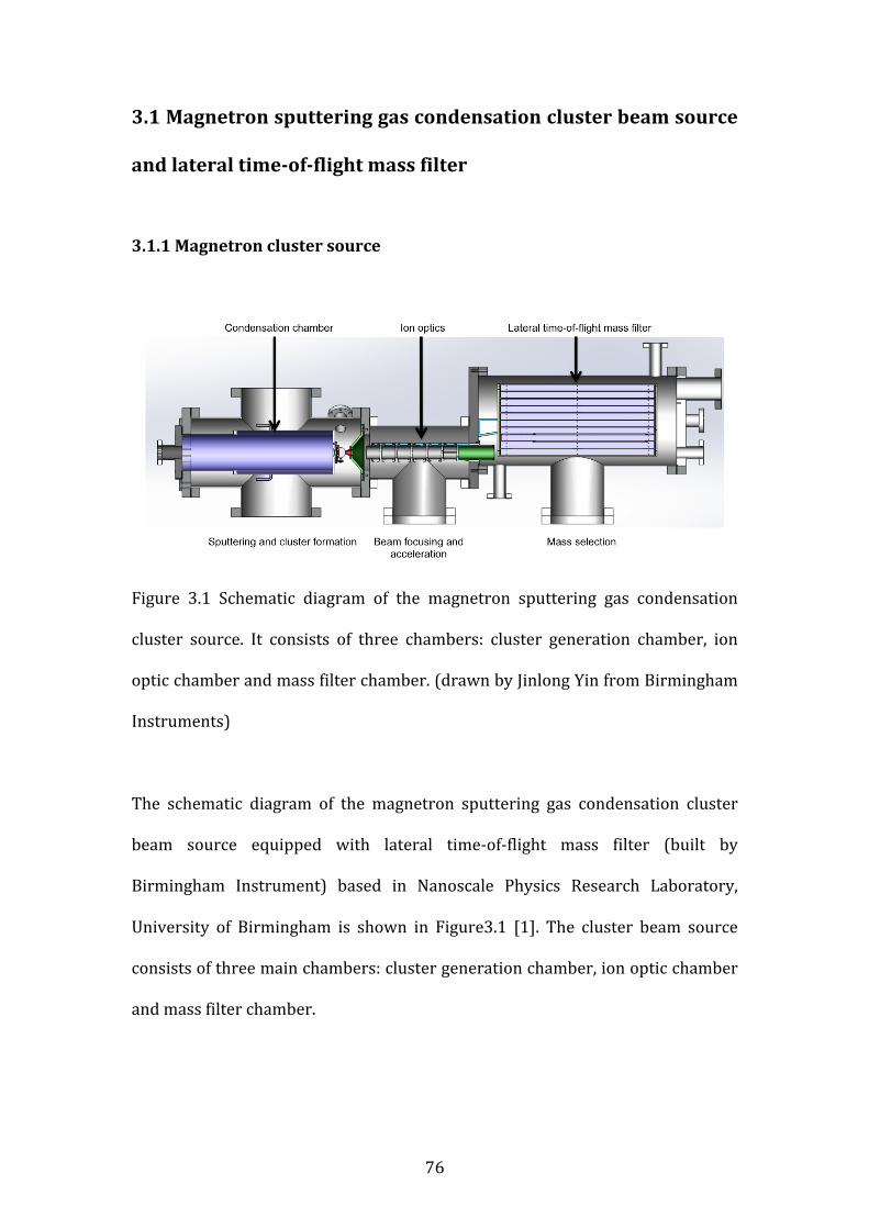
76
3.1 Magnetron sputtering gas condensation cluster beam source
and lateral time-‐of-‐flight mass filter
3.1.1 Magnetron cluster source
Figure 3.1 Schematic diagram of the magnetron sputtering gas condensation
cluster source. It consists of three chambers: cluster generation chamber, ion
optic chamber and mass filter chamber. (drawn by Jinlong Yin from Birmingham
Instruments)
The schematic diagram of the magnetron sputtering gas condensation cluster
beam source equipped with lateral time-‐of-‐flight mass filter (built by
Birmingham Instrument) based in Nanoscale Physics Research Laboratory,
University of Birmingham is shown in Figure3.1 [1]. The cluster beam source
consists of three main chambers: cluster generation chamber, ion optic chamber
and mass filter chamber.
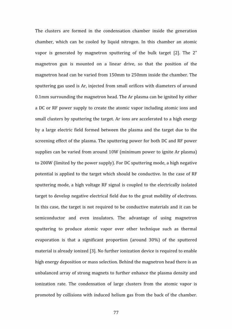
77
The clusters are formed in the condensation chamber inside the generation
chamber, which can be cooled by liquid nitrogen. In this chamber an atomic
vapor is generated by magnetron sputtering of the bulk target [2]. The 2”
magnetron gun is mounted on a linear drive, so that the position of the
magnetron head can be varied from 150mm to 250mm inside the chamber. The
sputtering gas used is Ar, injected from small orifices with diameters of around
0.1mm surrounding the magnetron head. The Ar plasma can be ignited by either
a DC or RF power supply to create the atomic vapor including atomic ions and
small clusters by sputtering the target. Ar ions are accelerated to a high energy
by a large electric field formed between the plasma and the target due to the
screening effect of the plasma. The sputtering power for both DC and RF power
supplies can be varied from around 10W (minimum power to ignite Ar plasma)
to 200W (limited by the power supply). For DC sputtering mode, a high negative
potential is applied to the target which should be conductive. In the case of RF
sputtering mode, a high voltage RF signal is coupled to the electrically isolated
target to develop negative electrical field due to the great mobility of electrons.
In this case, the target is not required to be conductive materials and it can be
semiconductor and even insulators. The advantage of using magnetron
sputtering to produce atomic vapor over other technique such as thermal
evaporation is that a significant proportion (around 30%) of the sputtered
material is already ionized [3]. No further ionization device is required to enable
high energy deposition or mass selection. Behind the magnetron head there is an
unbalanced array of strong magnets to further enhance the plasma density and
ionization rate. The condensation of large clusters from the atomic vapor is
promoted by collisions with induced helium gas from the back of the chamber.
78
The roles of the helium gas are not only for collision but also as the seeds for the
formation of clusters at nucleation stage [4-‐9]. Both Ar and He flow rates are
controlled by the mass flow controllers each with a maximum flow rate of 200
sccm. An adjustable nozzle (iris), 1mm to 10mm in diameter, is mounted at the
end of the condensation chamber enabling control of the pressure in
condensation chamber independently to the gas flow rate.
Clusters extracted from the condensation chamber are focused into a cluster
beam in the ion optic chamber by applying an electrical field after supersonic
expansion from the skimmer (5mm in diameter). All the ion optic lenses are
negatively biased as well as nozzle and skimmer (biased with low negative
voltage) as the mass filter of the cluster source has been designed to only select
positively charged particles. We only select clusters propagating parallel to the
axis of the cluster beam source, as the mass resolution is sensitive to the beam
focus at the end of the mass filter. The ion optics system consists of 7 cylindrical
lenses including a XY deflector and electrical field is created along the ion optic
axis to focus cluster ions. Five lenses, lens1, lens2, lens3 and XY lenses, are
connected to independent power supplies while the other two are biased to the
beam potential which is 500V here. The power supplies for the ion optic lenses
are the high voltage modules from Applied Kilovoltage up to -‐2.5kV. The beam
potential is powered by a power supply from Glassman FL series up to -‐1kV. The
optimum voltage settings on each lens vary with the size of selected clusters and
the rough range is obtained by the simulation of the cluster beam trajectory in
SIMION 8.1 [10]. The shape of the focused cluster beam passing through the ion
79
optics can be monitored by a Faraday cup at the white beam exit (the bottom exit
of the mass filter).
3.1.2 Working principle of the lateral time-‐of-‐flight (ToF) mass filter
The focused cluster ion beam is then mass selected by the lateral time-‐of-‐flight
(ToF) mass filter installed in the third chamber [11]. In the lateral ToF mass
filter, a portion of the cluster ion beam is accelerated perpendicular to its
original flight direction with a pulsed electric field in the bottom region and then
stopped at the top region of the mass filter by another opposite pulsed electric
field after letting it fly in the middle for a certain time. The cluster beam is
therefore effectively spread out vertically after entering the mass filter and the
magnitude of the displacement of the cluster ion beam under the same electric
pulse is dependent on the charge mass ratio of the clusters and nearly all cluster
ions are single charged. The mass selection is achieved with an aperture placed
at the end of top region only allowing a small portion of the displaced ion beam
flying through.
The schematic diagram of the lateral ToF mass filter is shown in Figure 3.2 [11].
The bottom region of the mass filter is called the acceleration region where the
cluster ion beam is kicked upward by a pulsed electrical field. The middle region
is called the flight region where is field free between two pulses. The top region
is the deceleration region where the perpendicular movement is stopped by
another opposite kick. The cluster beam enters the mass filter from the left side.
A Faraday cup is mounted at the end of the bottom region, which should be the
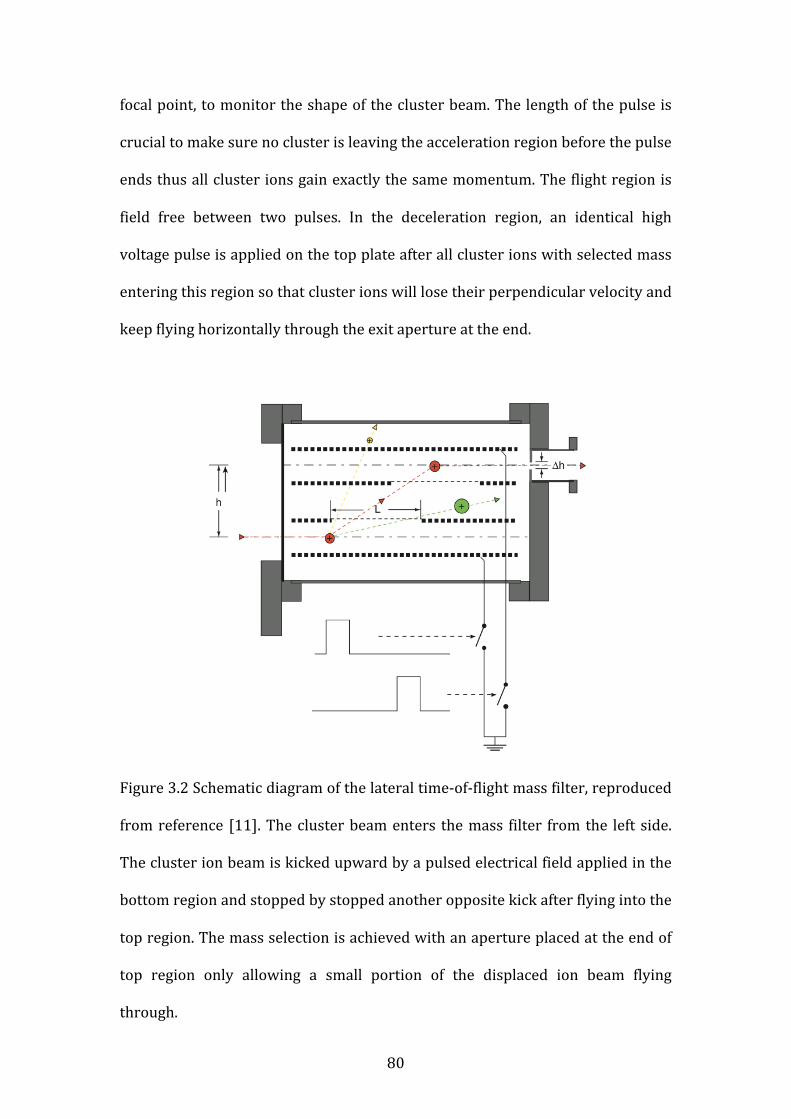
80
focal point, to monitor the shape of the cluster beam. The length of the pulse is
crucial to make sure no cluster is leaving the acceleration region before the pulse
ends thus all cluster ions gain exactly the same momentum. The flight region is
field free between two pulses. In the deceleration region, an identical high
voltage pulse is applied on the top plate after all cluster ions with selected mass
entering this region so that cluster ions will lose their perpendicular velocity and
keep flying horizontally through the exit aperture at the end.
Figure 3.2 Schematic diagram of the lateral time-‐of-‐flight mass filter, reproduced
from reference [11]. The cluster beam enters the mass filter from the left side.
The cluster ion beam is kicked upward by a pulsed electrical field applied in the
bottom region and stopped by stopped another opposite kick after flying into the
top region. The mass selection is achieved with an aperture placed at the end of
top region only allowing a small portion of the displaced ion beam flying
through.
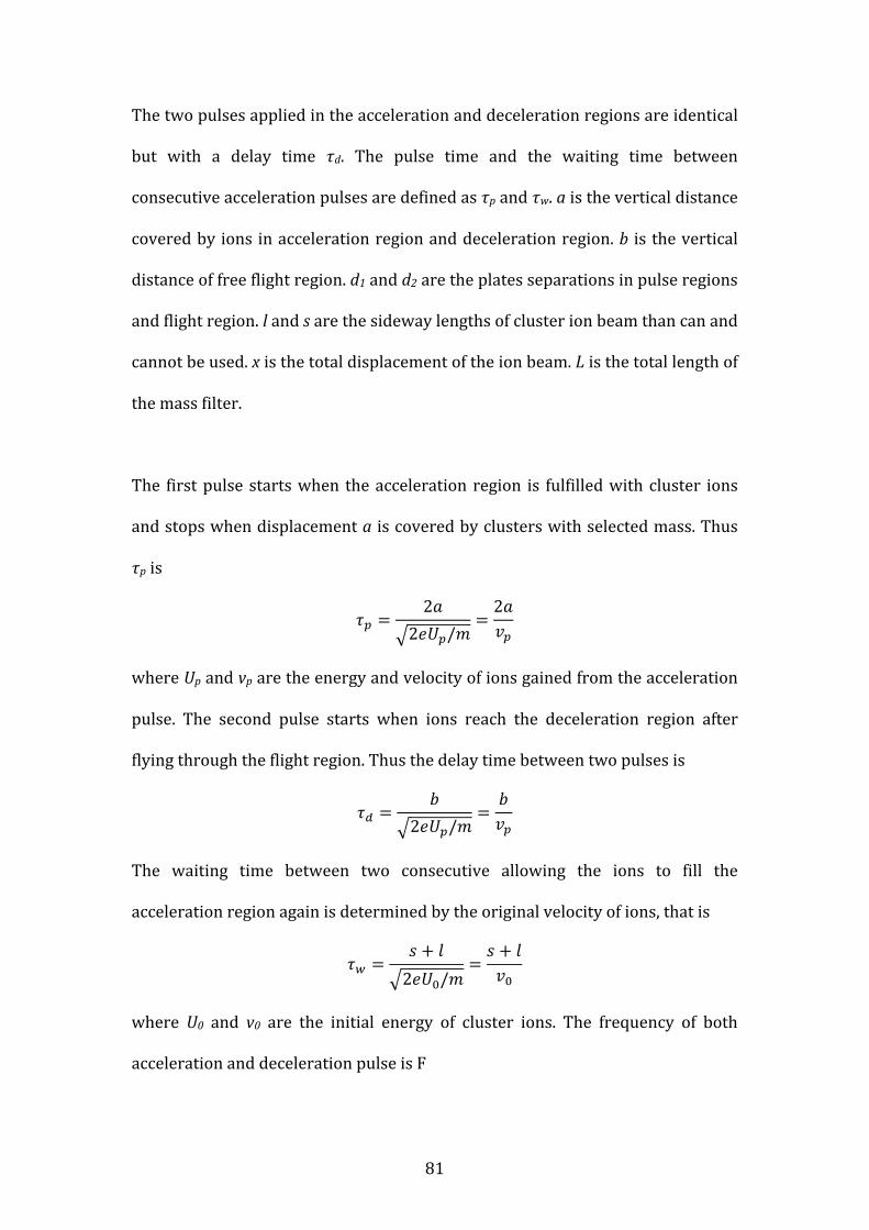
81
The two pulses applied in the acceleration and deceleration regions are identical
but with a delay time τd. The pulse time and the waiting time between
consecutive acceleration pulses are defined as τp and τw. a is the vertical distance
covered by ions in acceleration region and deceleration region. b is the vertical
distance of free flight region. d1 and d2 are the plates separations in pulse regions
and flight region. l and s are the sideway lengths of cluster ion beam than can and
cannot be used. x is the total displacement of the ion beam. L is the total length of
the mass filter.
The first pulse starts when the acceleration region is fulfilled with cluster ions
and stops when displacement a is covered by clusters with selected mass. Thus
τp is
𝜏! =2𝑎
2𝑒𝑈!/𝑚=2𝑎𝑣!
where Up and vp are the energy and velocity of ions gained from the acceleration
pulse. The second pulse starts when ions reach the deceleration region after
flying through the flight region. Thus the delay time between two pulses is
𝜏! =𝑏
2𝑒𝑈!/𝑚=𝑏𝑣!
The waiting time between two consecutive allowing the ions to fill the
acceleration region again is determined by the original velocity of ions, that is
𝜏! =𝑠 + 𝑙2𝑒𝑈!/𝑚
=𝑠 + 𝑙𝑣!
where U0 and v0 are the initial energy of cluster ions. The frequency of both
acceleration and deceleration pulse is F
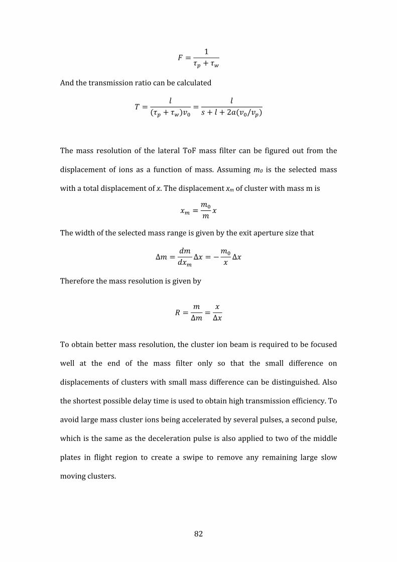
82
𝐹 =1
𝜏! + 𝜏!
And the transmission ratio can be calculated
𝑇 =𝑙
(𝜏! + 𝜏!)𝑣!=
𝑙𝑠 + 𝑙 + 2𝑎(𝑣!/𝑣!)
The mass resolution of the lateral ToF mass filter can be figured out from the
displacement of ions as a function of mass. Assuming m0 is the selected mass
with a total displacement of x. The displacement xm of cluster with mass m is
𝑥! =𝑚!
𝑚 𝑥
The width of the selected mass range is given by the exit aperture size that
∆𝑚 =𝑑𝑚𝑑𝑥!
∆𝑥 = −𝑚!
𝑥 ∆𝑥
Therefore the mass resolution is given by
𝑅 =
𝑚∆𝑚 =
𝑥∆𝑥
To obtain better mass resolution, the cluster ion beam is required to be focused
well at the end of the mass filter only so that the small difference on
displacements of clusters with small mass difference can be distinguished. Also
the shortest possible delay time is used to obtain high transmission efficiency. To
avoid large mass cluster ions being accelerated by several pulses, a second pulse,
which is the same as the deceleration pulse is also applied to two of the middle
plates in flight region to create a swipe to remove any remaining large slow
moving clusters.
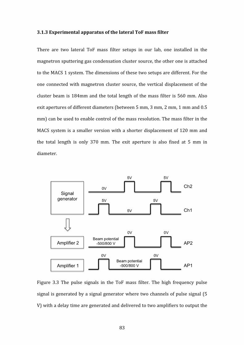
83
3.1.3 Experimental apparatus of the lateral ToF mass filter
There are two lateral ToF mass filter setups in our lab, one installed in the
magnetron sputtering gas condensation cluster source, the other one is attached
to the MACS 1 system. The dimensions of these two setups are different. For the
one connected with magnetron cluster source, the vertical displacement of the
cluster beam is 184mm and the total length of the mass filter is 560 mm. Also
exit apertures of different diameters (between 5 mm, 3 mm, 2 mm, 1 mm and 0.5
mm) can be used to enable control of the mass resolution. The mass filter in the
MACS system is a smaller version with a shorter displacement of 120 mm and
the total length is only 370 mm. The exit aperture is also fixed at 5 mm in
diameter.
Figure 3.3 The pulse signals in the ToF mass filter. The high frequency pulse
signal is generated by a signal generator where two channels of pulse signal (5
V) with a delay time are generated and delivered to two amplifiers to output the
84
high voltage pulsed signal (500/800 V) for acceleration and deceleration regions.
The pulse width is set as 20% of the total pulse period and the delay time is 50%
of the total period between two pulses.
The electronics of these two ToF mass filters are exactly the same. The high
frequency pulse signal is generated by a signal generator from BNC (575-‐2h)
where two channels of pulse signal (5 V) with a delay time are generated and
delivered to two amplifiers from DEI (PVX4150) to output the high voltage
pulsed signal for acceleration and deceleration regions as illustrated in Figure
3.3. The magnitude of the pulse is controlled by the beam potential voltage,
which is applied by the high voltage powersupply from Glassman (FL series). The
beam potential in the magnetron cluster beam source is set at -‐500 V, while -‐800
V in the MACS system. Both channels of pulse signals generated from the BNC
single generator are square waves with magnitude of 5 V.
For these two mass filter systems the pulse signals are nearly identical except
the frequency for the selected size varies slightly due to different total
displacement. The pulse width is set as 20% of the total pulse period and the
delay time is 50% of the total period between two pulses. The pulse signals are
then amplified by two pulse generators before being delivered to the mass filter.
For each pulse generator, it has two input channels and one output channel. The
two input channels are connected to beam potential (Low) and ground (High)
respectively. The output channel is connected to the assigned plates of the mass
filter and output voltage is the difference between the Low and High input
voltages dependent on the gate voltage (5V or 0V) which is a square wave signal.
85
All the plates of the ToF mass filter are biased at the beam potential when pulse
is off. When pulse is on, the plates in the acceleration or deceleration regions are
switched from beam potential to 0 V to give positive cluster ions a kick. For the
mass filter in the MACS system, which has a vertical displacement of 120mm, the
optimal pulse frequency of selected Ar clusters (mass=40 amu) is 203kHz, based
on which frequency of any selected mass can be calculated.
3.1.4 Operation of the magnetron sputtering cluster source and sample
deposition
The operation of the magnetron sputtering cluster source can be divided into
following steps: preparation work, plasma ignition, optimization of the cluster
beam (including tuning condensation conditions and ion optics, and mass
spectra) and sample deposition.
Preparation work
The preparation work before producing clusters includes changing the target,
cooling, mounting samples onto the sample holder and pumping down the
chambers. Usually the base pressure of the cluster source is lower than 10-‐6
mbar in the generation chamber and 10-‐7~10-‐8 mbar in ion optic chamber, mass
filter chamber and deposition chamber. Liquid nitrogen cooling of the
condensation chamber is also a necessity to prompt condensation when making
large size clusters. The cooling process usually takes 1 hour from room
temperature to ~77K.
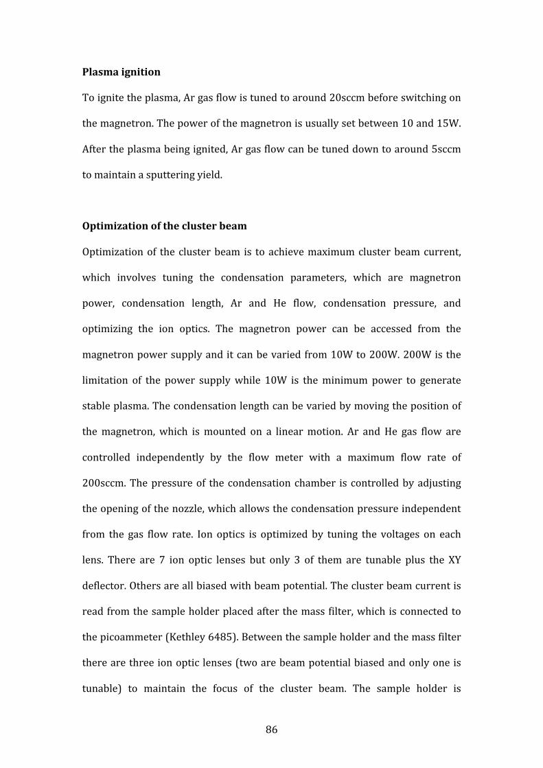
86
Plasma ignition
To ignite the plasma, Ar gas flow is tuned to around 20sccm before switching on
the magnetron. The power of the magnetron is usually set between 10 and 15W.
After the plasma being ignited, Ar gas flow can be tuned down to around 5sccm
to maintain a sputtering yield.
Optimization of the cluster beam
Optimization of the cluster beam is to achieve maximum cluster beam current,
which involves tuning the condensation parameters, which are magnetron
power, condensation length, Ar and He flow, condensation pressure, and
optimizing the ion optics. The magnetron power can be accessed from the
magnetron power supply and it can be varied from 10W to 200W. 200W is the
limitation of the power supply while 10W is the minimum power to generate
stable plasma. The condensation length can be varied by moving the position of
the magnetron, which is mounted on a linear motion. Ar and He gas flow are
controlled independently by the flow meter with a maximum flow rate of
200sccm. The pressure of the condensation chamber is controlled by adjusting
the opening of the nozzle, which allows the condensation pressure independent
from the gas flow rate. Ion optics is optimized by tuning the voltages on each
lens. There are 7 ion optic lenses but only 3 of them are tunable plus the XY
deflector. Others are all biased with beam potential. The cluster beam current is
read from the sample holder placed after the mass filter, which is connected to
the picoammeter (Kethley 6485). Between the sample holder and the mass filter
there are three ion optic lenses (two are beam potential biased and only one is
tunable) to maintain the focus of the cluster beam. The sample holder is
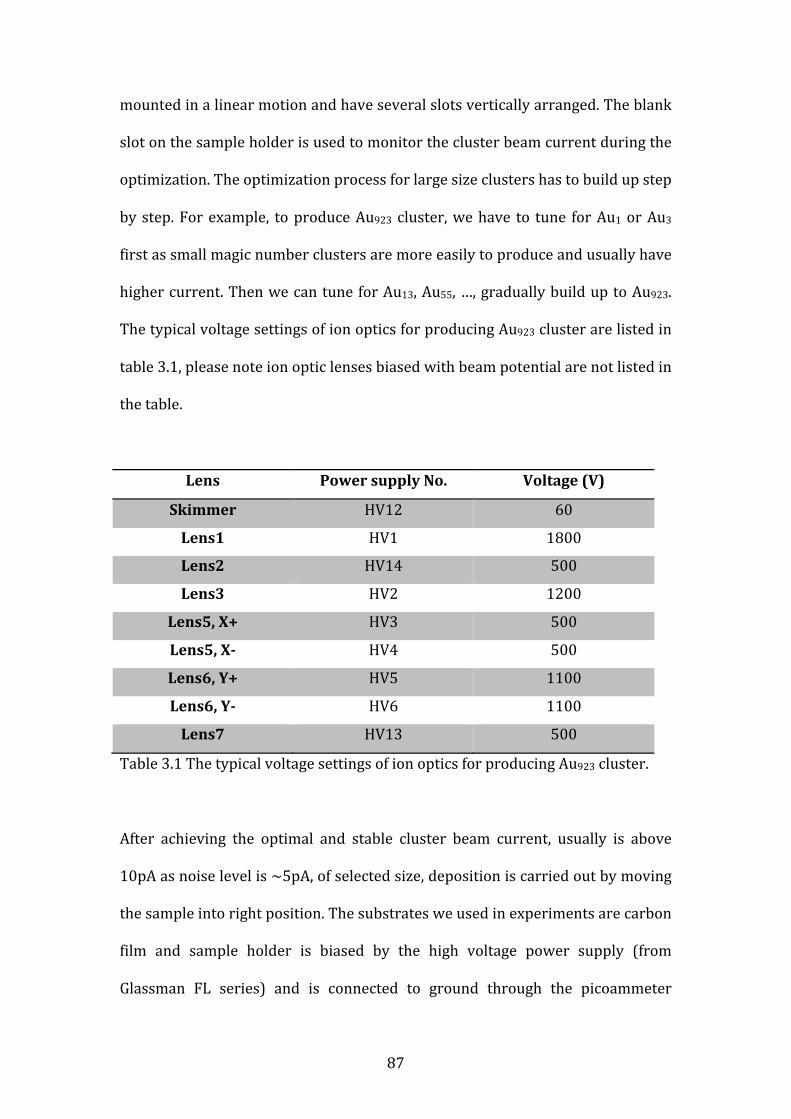
87
mounted in a linear motion and have several slots vertically arranged. The blank
slot on the sample holder is used to monitor the cluster beam current during the
optimization. The optimization process for large size clusters has to build up step
by step. For example, to produce Au923 cluster, we have to tune for Au1 or Au3
first as small magic number clusters are more easily to produce and usually have
higher current. Then we can tune for Au13, Au55, …, gradually build up to Au923.
The typical voltage settings of ion optics for producing Au923 cluster are listed in
table 3.1, please note ion optic lenses biased with beam potential are not listed in
the table.
Lens Power supply No. Voltage (V)
Skimmer HV12 60
Lens1 HV1 1800
Lens2 HV14 500
Lens3 HV2 1200
Lens5, X+ HV3 500
Lens5, X-‐ HV4 500
Lens6, Y+ HV5 1100
Lens6, Y-‐ HV6 1100
Lens7 HV13 500
Table 3.1 The typical voltage settings of ion optics for producing Au923 cluster.
After achieving the optimal and stable cluster beam current, usually is above
10pA as noise level is ~5pA, of selected size, deposition is carried out by moving
the sample into right position. The substrates we used in experiments are carbon
film and sample holder is biased by the high voltage power supply (from
Glassman FL series) and is connected to ground through the picoammeter
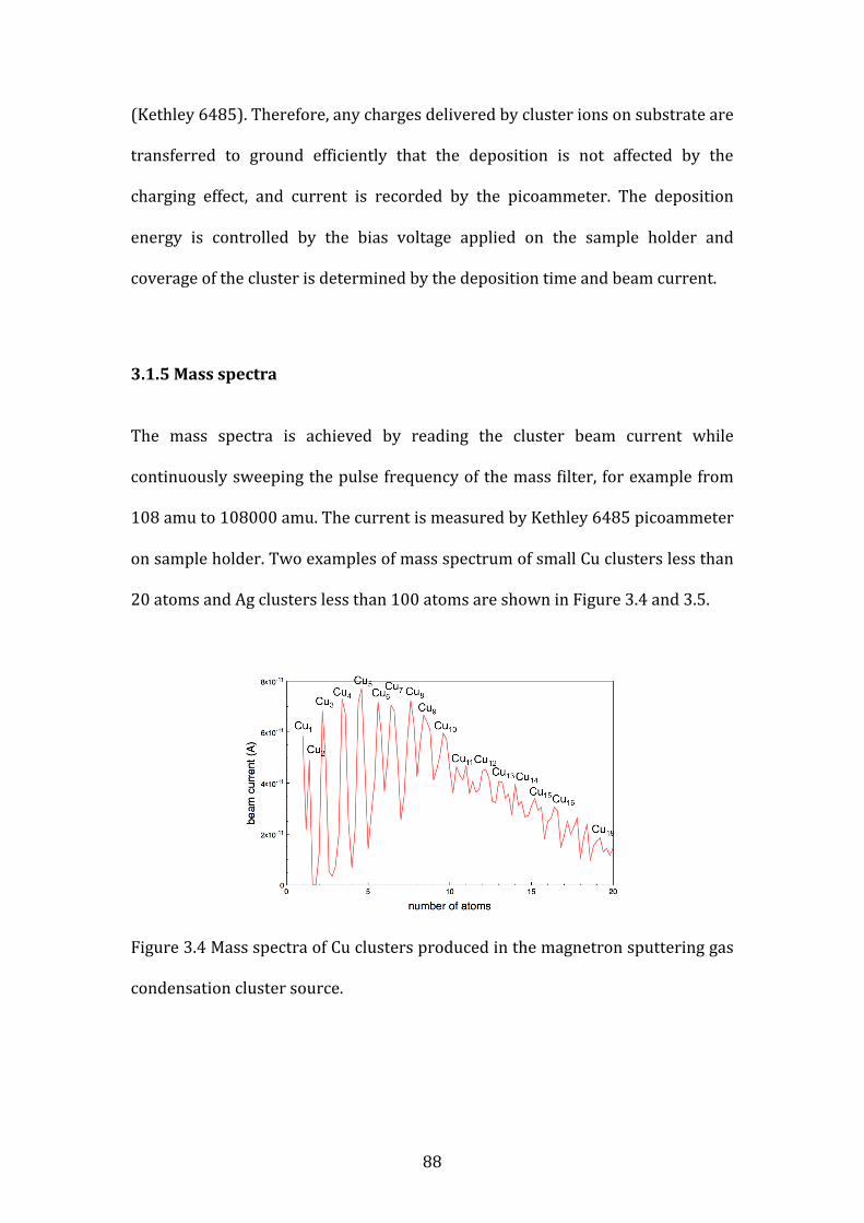
88
(Kethley 6485). Therefore, any charges delivered by cluster ions on substrate are
transferred to ground efficiently that the deposition is not affected by the
charging effect, and current is recorded by the picoammeter. The deposition
energy is controlled by the bias voltage applied on the sample holder and
coverage of the cluster is determined by the deposition time and beam current.
3.1.5 Mass spectra
The mass spectra is achieved by reading the cluster beam current while
continuously sweeping the pulse frequency of the mass filter, for example from
108 amu to 108000 amu. The current is measured by Kethley 6485 picoammeter
on sample holder. Two examples of mass spectrum of small Cu clusters less than
20 atoms and Ag clusters less than 100 atoms are shown in Figure 3.4 and 3.5.
Figure 3.4 Mass spectra of Cu clusters produced in the magnetron sputtering gas
condensation cluster source.
89
Figure 3.5 Mass spectra of Ag clusters produced in the magnetron sputtering gas
condensation cluster source.
3.2 Aberration corrected scanning transmission electron
microscope
3.2.1 Overview of JEOL 2100F
The electron microscope based in Nanoscale Physics Research Laboratory,
University of Birmingham is a JEOL 2100F scanning transmission electron
microscope (STEM) with CEOS aberration corrector up to the fifth order. The
photograph and schematic diagram of internal structure of JEOL 2100F is shown
in Figure 3.6.
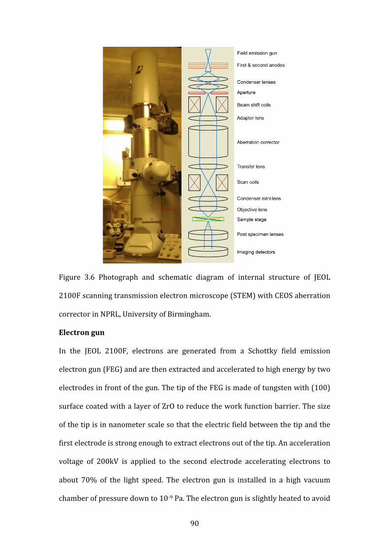
90
Figure 3.6 Photograph and schematic diagram of internal structure of JEOL
2100F scanning transmission electron microscope (STEM) with CEOS aberration
corrector in NPRL, University of Birmingham.
Electron gun
In the JEOL 2100F, electrons are generated from a Schottky field emission
electron gun (FEG) and are then extracted and accelerated to high energy by two
electrodes in front of the gun. The tip of the FEG is made of tungsten with (100)
surface coated with a layer of ZrO to reduce the work function barrier. The size
of the tip is in nanometer scale so that the electric field between the tip and the
first electrode is strong enough to extract electrons out of the tip. An acceleration
voltage of 200kV is applied to the second electrode accelerating electrons to
about 70% of the light speed. The electron gun is installed in a high vacuum
chamber of pressure down to 10-‐9 Pa. The electron gun is slightly heated to avoid
91
contamination and to promote the emission efficiency. The focused electron
beam probe is formed by electrons passing through 3 stages of electron optics
system and the aberration of the electron beam is corrected by the aberration
corrector prior to the specimen.
Electron optics
The working principle of the electron optics system is to generate
electromagnetic fields by the lens coils in the condenser lens system to collimate
and focus the electrons. Additionally, further coils are used to align the electron
beam with the sample by tilting and shifting the beam. A set of apertures is
mounted after the condenser lens system to remove the widely scattered
electrons, and the most common aperture we used is 40μm in diameter.
Aberration corrector
The aberration correction system is installed after the condenser lens and
aperture, where the aberration induced by the condenser lens is compensated. In
our JEOL 2100F STEM, the aberration corrector used is CEOS double hexapole
spherical aberration corrector consisting of two sets of 6 pole pieces and two
sets of transfer lenses in the middle. An approximately circular field is generated
by the two sets of hexapole elements with the dedicated rotational offset
alignment to form a negative spherical aberration equivalent to the positive
aberration induced by condenser lenses. The electron beam passing through the
aberration corrector is then focused into a probe by the objective lens prior to
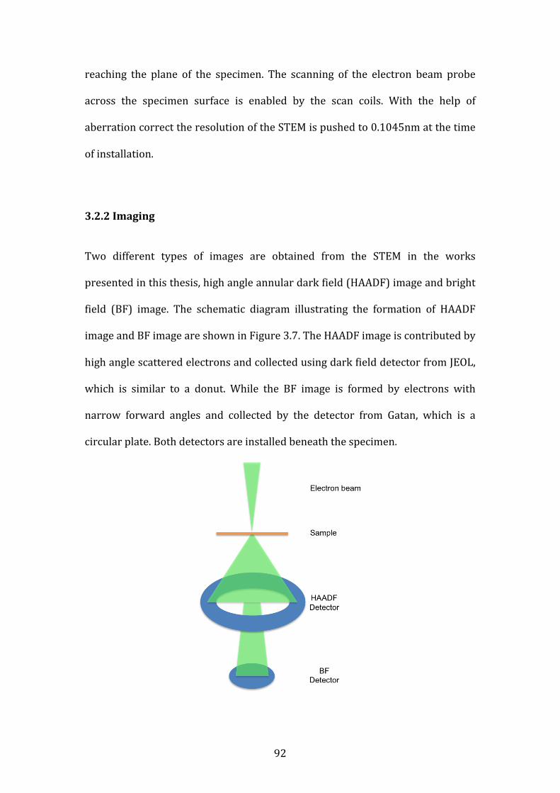
92
reaching the plane of the specimen. The scanning of the electron beam probe
across the specimen surface is enabled by the scan coils. With the help of
aberration correct the resolution of the STEM is pushed to 0.1045nm at the time
of installation.
3.2.2 Imaging
Two different types of images are obtained from the STEM in the works
presented in this thesis, high angle annular dark field (HAADF) image and bright
field (BF) image. The schematic diagram illustrating the formation of HAADF
image and BF image are shown in Figure 3.7. The HAADF image is contributed by
high angle scattered electrons and collected using dark field detector from JEOL,
which is similar to a donut. While the BF image is formed by electrons with
narrow forward angles and collected by the detector from Gatan, which is a
circular plate. Both detectors are installed beneath the specimen.
93
Figure 3.7 Schematic diagram illustrating the positions of HAADF detector and
BF detector.
The advantages of HAADF image are that it exhibits sound atomic resolution and
contains the quantitative information. HAADF images are formed by high angle
scattered electrons which lose the coherence if the collection angle is large
enough that the inner collection angle is more than three times of the beam
convergence semi-‐angle (about 50 mrad). In that case, the electrons to form the
HAADF image are not affected by the complicated phase change, instead they are
determined by the elemental atomic number and the thickness and can be
described by Rutherford scattering equation. The intensity of HAADF STEM
image formed by high angle scattered incoherent electrons which follow the
Rutherfold scattering equation is proportional to Z2, Z is the atomic number.
However, in reality the power exponent is affected by the screening of nuclear
charge that the equation has to be modified to I~tZα, α is usually varied with
camera length in the STEM, which determines collection angle and convergence
angle. In our STEM, the power exponent α is calibrated with help of size selected
nanoclusters Au923 and Pd923 by ZW. Wang in 2011 for the condition of the inner
and outer collection angle of 62 and 164mrad and convergence angle of 19mrad
[12]. In the calibration, average intensities of size selected Au923 and Pd923 are
measured respectively over large populations. The power exponent α is then
obtained based on the equation
𝐼!"𝐼!"
= (𝑍!"𝑍!"
)!
that α=1.46±0.18 [12].
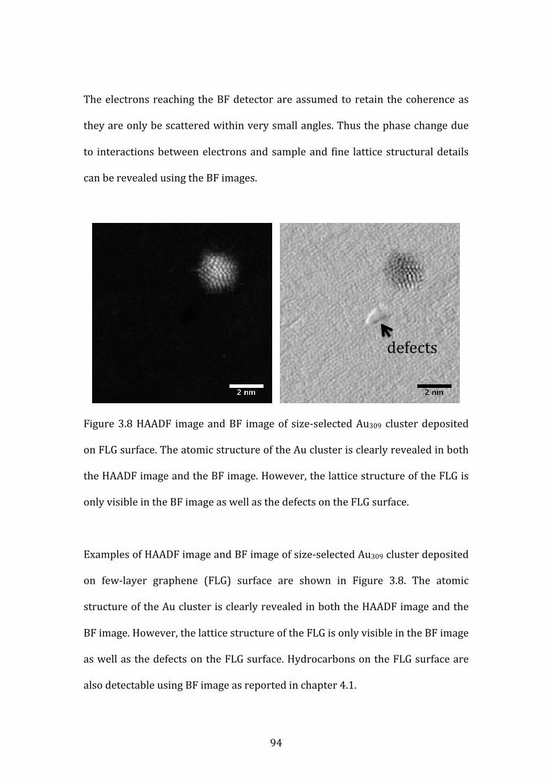
94
The electrons reaching the BF detector are assumed to retain the coherence as
they are only be scattered within very small angles. Thus the phase change due
to interactions between electrons and sample and fine lattice structural details
can be revealed using the BF images.
Figure 3.8 HAADF image and BF image of size-‐selected Au309 cluster deposited
on FLG surface. The atomic structure of the Au cluster is clearly revealed in both
the HAADF image and the BF image. However, the lattice structure of the FLG is
only visible in the BF image as well as the defects on the FLG surface.
Examples of HAADF image and BF image of size-‐selected Au309 cluster deposited
on few-‐layer graphene (FLG) surface are shown in Figure 3.8. The atomic
structure of the Au cluster is clearly revealed in both the HAADF image and the
BF image. However, the lattice structure of the FLG is only visible in the BF image
as well as the defects on the FLG surface. Hydrocarbons on the FLG surface are
also detectable using BF image as reported in chapter 4.1.
defects
95
On the other hand, HAADF image has its irreplaceable advantage, which is
quantitative information. For example, the intensity of the size-‐selected Au309
cluster can be used as the mass balance to measure the thickness of the graphene
film, which is used in Chapter 4.1 to determine the number of layers of the FLG.
Also in chapter 5 and chapter 6, the number of atoms of clusters produced in the
matrix assembly cluster source is measured by the HAADF intensity of single
atoms and size-‐selected Au923 clusters.
3.2.3 Effect of electron beam
The effect of high-‐energy electron beam on nanocluster structures has already
been investigated by Wang and Palmer in 2012, where they found the structure
of Au923 cluster is transferring under the electron beam from icosahedral to
decahedral or fcc. The mechanism of the structural transformation under high-‐
energy electron is that nanoclusters absorb energy from the electron beam to
drive them through the energy threshold to reach more equilibrated state. The
same phenomenon is also observed in our work when successively taking
images on the same Au923 cluster. The time between each photo shoot is 5s and
the structure of the Au923 is changed from icosahedral to fcc after 160s. The first
shoot HAADF image and images taken at 30s, 80s and 160s are shown in Figure
3.9.
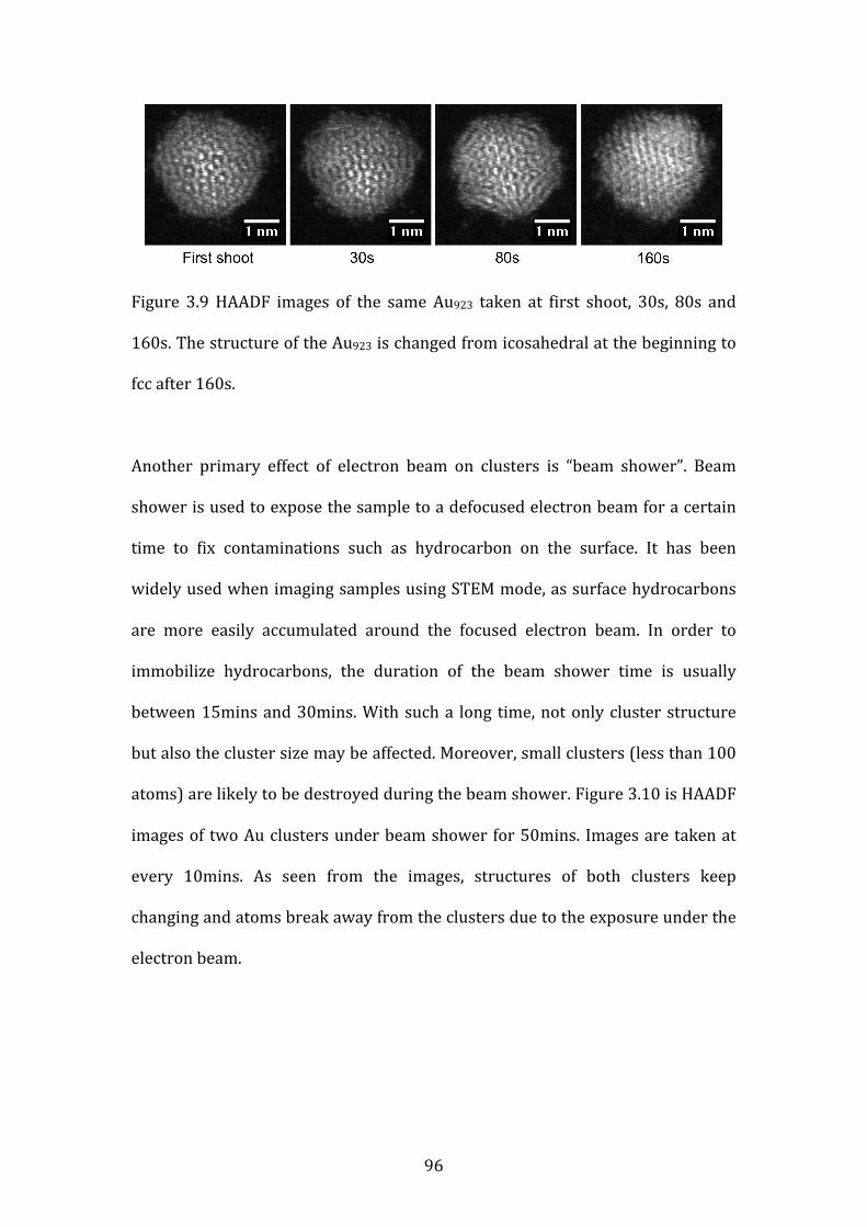
96
Figure 3.9 HAADF images of the same Au923 taken at first shoot, 30s, 80s and
160s. The structure of the Au923 is changed from icosahedral at the beginning to
fcc after 160s.
Another primary effect of electron beam on clusters is “beam shower”. Beam
shower is used to expose the sample to a defocused electron beam for a certain
time to fix contaminations such as hydrocarbon on the surface. It has been
widely used when imaging samples using STEM mode, as surface hydrocarbons
are more easily accumulated around the focused electron beam. In order to
immobilize hydrocarbons, the duration of the beam shower time is usually
between 15mins and 30mins. With such a long time, not only cluster structure
but also the cluster size may be affected. Moreover, small clusters (less than 100
atoms) are likely to be destroyed during the beam shower. Figure 3.10 is HAADF
images of two Au clusters under beam shower for 50mins. Images are taken at
every 10mins. As seen from the images, structures of both clusters keep
changing and atoms break away from the clusters due to the exposure under the
electron beam.
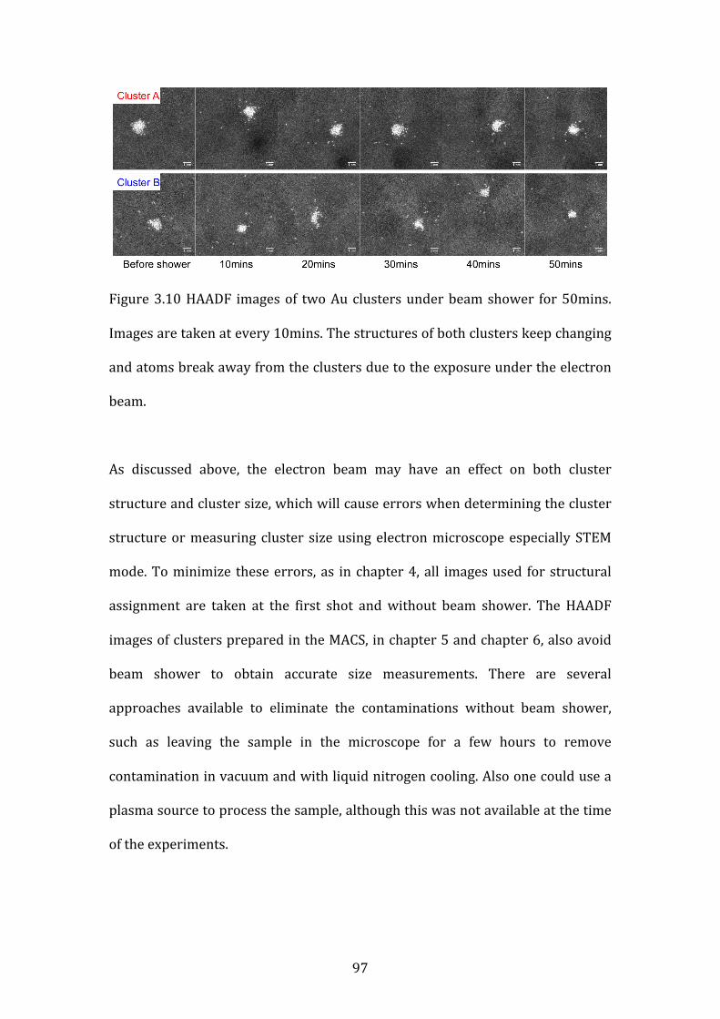
97
Figure 3.10 HAADF images of two Au clusters under beam shower for 50mins.
Images are taken at every 10mins. The structures of both clusters keep changing
and atoms break away from the clusters due to the exposure under the electron
beam.
As discussed above, the electron beam may have an effect on both cluster
structure and cluster size, which will cause errors when determining the cluster
structure or measuring cluster size using electron microscope especially STEM
mode. To minimize these errors, as in chapter 4, all images used for structural
assignment are taken at the first shot and without beam shower. The HAADF
images of clusters prepared in the MACS, in chapter 5 and chapter 6, also avoid
beam shower to obtain accurate size measurements. There are several
approaches available to eliminate the contaminations without beam shower,
such as leaving the sample in the microscope for a few hours to remove
contamination in vacuum and with liquid nitrogen cooling. Also one could use a
plasma source to process the sample, although this was not available at the time
of the experiments.
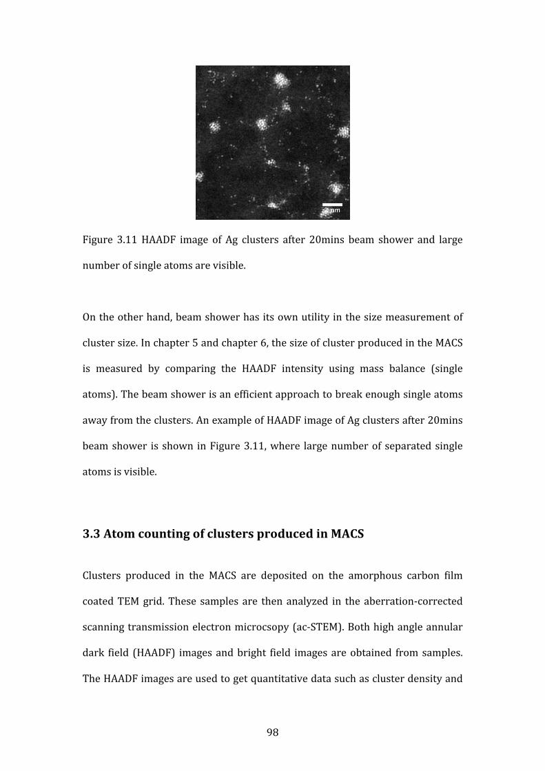
98
Figure 3.11 HAADF image of Ag clusters after 20mins beam shower and large
number of single atoms are visible.
On the other hand, beam shower has its own utility in the size measurement of
cluster size. In chapter 5 and chapter 6, the size of cluster produced in the MACS
is measured by comparing the HAADF intensity using mass balance (single
atoms). The beam shower is an efficient approach to break enough single atoms
away from the clusters. An example of HAADF image of Ag clusters after 20mins
beam shower is shown in Figure 3.11, where large number of separated single
atoms is visible.
3.3 Atom counting of clusters produced in MACS
Clusters produced in the MACS are deposited on the amorphous carbon film
coated TEM grid. These samples are then analyzed in the aberration-‐corrected
scanning transmission electron microcsopy (ac-‐STEM). Both high angle annular
dark field (HAADF) images and bright field images are obtained from samples.
The HAADF images are used to get quantitative data such as cluster density and
99
cluster size distribution, while bright field images provide cluster structures in
better contrast. The cluster flux is calculated based on the cluster density
measured from HAADF STEM images then divided by deposition time instead of
directly measuring the current. Two reasons are: not all the clusters produced
are positively charged, as there are also negatively charged and most portion is
neutral as found in the charge fraction experiment later. The current measured
on the cold finger is a mixture of cluster beam current, Ar ion beam current
through the matrix and secondary electron generates during the collisions when
the Ar ion beam hits the matrix. The size of clusters is measured from the
integrated HAADF intensity by comparing with the HAADF intensity of mass
balance, which is single atom here. Single atoms can only be seen at high
magnification in STEM that atoms are coming off due to the fragmentation of
clusters under high energy electron beam [13-‐14]. In order to avoid clusters
damaged by the electron beam, the HAADF images of clusters is taken at low
magnification (2Mx). Moreover, different pixel sizes are usually used in high and
low magnification images. Generally, HAADF intensity of a cluster or single atom
at different magnifications and different resolutions can be described by the
following equation, where the HAADF intensity is proportional to pixels that the
cluster takes times the time electron beam scanning over one pixel.
𝑰 ∝ 𝑲×𝑨𝒓𝒆𝒂 𝒕𝒐𝒕𝒂𝒍 𝒑𝒊𝒙𝒆𝒍𝒔 𝒄𝒐𝒗𝒆𝒓𝒆𝒅 𝒃𝒚 𝒄𝒍𝒖𝒔𝒕𝒆𝒓
×𝑻𝒊𝒎𝒆(𝒆𝒍𝒆𝒄𝒕𝒓𝒐𝒏 𝒃𝒆𝒂𝒎 𝒔𝒄𝒂𝒏𝒏𝒊𝒏𝒈 𝒐𝒗𝒆𝒓 𝒐𝒏𝒆 𝒑𝒊𝒙𝒆𝒍)
Here K is related to the settings in the microscope. In this work, all the settings
(energy of electron beam, camera length, spot area, contrast and brightness) are
not changed that K can be regard as a constant. The time for the electron beam to
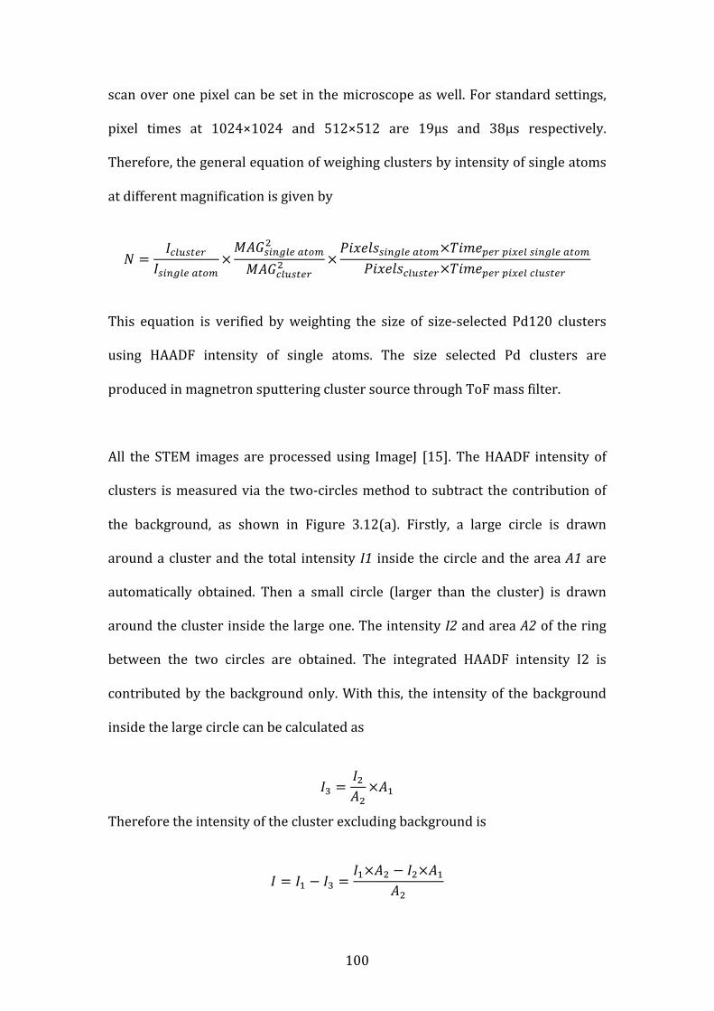
100
scan over one pixel can be set in the microscope as well. For standard settings,
pixel times at 1024×1024 and 512×512 are 19μs and 38μs respectively.
Therefore, the general equation of weighing clusters by intensity of single atoms
at different magnification is given by
𝑁 =𝐼!"#$%&'
𝐼!"#$%& !"#$×𝑀𝐴𝐺!"#$%& !"#$!
𝑀𝐴𝐺!"#$%&'! ×𝑃𝑖𝑥𝑒𝑙𝑠!"#$%& !"#$×𝑇𝑖𝑚𝑒!"# !"#$% !"#$%& !"#$
𝑃𝑖𝑥𝑒𝑙𝑠!"#$%&'×𝑇𝑖𝑚𝑒!"# !"#$% !"#$%&'
This equation is verified by weighting the size of size-‐selected Pd120 clusters
using HAADF intensity of single atoms. The size selected Pd clusters are
produced in magnetron sputtering cluster source through ToF mass filter.
All the STEM images are processed using ImageJ [15]. The HAADF intensity of
clusters is measured via the two-‐circles method to subtract the contribution of
the background, as shown in Figure 3.12(a). Firstly, a large circle is drawn
around a cluster and the total intensity I1 inside the circle and the area A1 are
automatically obtained. Then a small circle (larger than the cluster) is drawn
around the cluster inside the large one. The intensity I2 and area A2 of the ring
between the two circles are obtained. The integrated HAADF intensity I2 is
contributed by the background only. With this, the intensity of the background
inside the large circle can be calculated as
𝐼! =𝐼!𝐴!×𝐴!
Therefore the intensity of the cluster excluding background is
𝐼 = 𝐼! − 𝐼! =𝐼!×𝐴! − 𝐼!×𝐴!
𝐴!
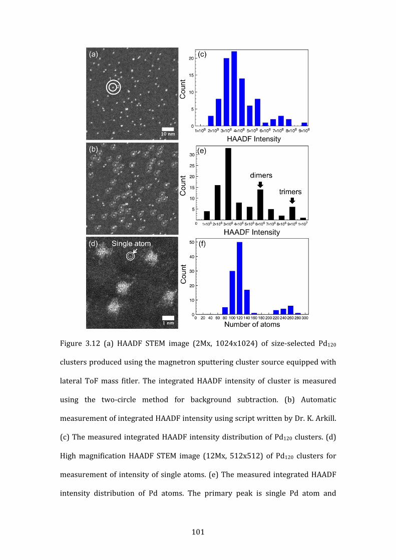
101
Figure 3.12 (a) HAADF STEM image (2Mx, 1024x1024) of size-‐selected Pd120
clusters produced using the magnetron sputtering cluster source equipped with
lateral ToF mass fitler. The integrated HAADF intensity of cluster is measured
using the two-‐circle method for background subtraction. (b) Automatic
measurement of integrated HAADF intensity using script written by Dr. K. Arkill.
(c) The measured integrated HAADF intensity distribution of Pd120 clusters. (d)
High magnification HAADF STEM image (12Mx, 512x512) of Pd120 clusters for
measurement of intensity of single atoms. (e) The measured integrated HAADF
intensity distribution of Pd atoms. The primary peak is single Pd atom and
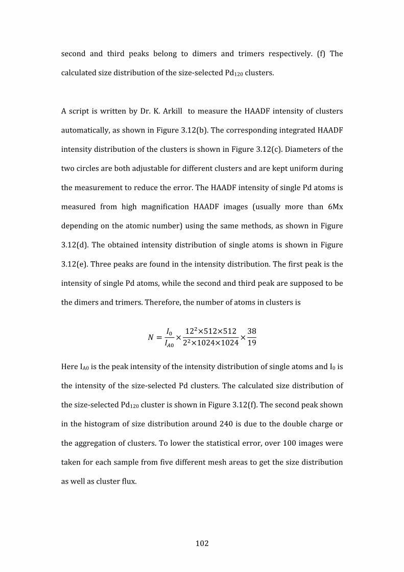
102
second and third peaks belong to dimers and trimers respectively. (f) The
calculated size distribution of the size-‐selected Pd120 clusters.
A script is written by Dr. K. Arkill to measure the HAADF intensity of clusters
automatically, as shown in Figure 3.12(b). The corresponding integrated HAADF
intensity distribution of the clusters is shown in Figure 3.12(c). Diameters of the
two circles are both adjustable for different clusters and are kept uniform during
the measurement to reduce the error. The HAADF intensity of single Pd atoms is
measured from high magnification HAADF images (usually more than 6Mx
depending on the atomic number) using the same methods, as shown in Figure
3.12(d). The obtained intensity distribution of single atoms is shown in Figure
3.12(e). Three peaks are found in the intensity distribution. The first peak is the
intensity of single Pd atoms, while the second and third peak are supposed to be
the dimers and trimers. Therefore, the number of atoms in clusters is
𝑁 =𝐼!𝐼!!
×12!×512×5122!×1024×1024×
3819
Here IA0 is the peak intensity of the intensity distribution of single atoms and I0 is
the intensity of the size-‐selected Pd clusters. The calculated size distribution of
the size-‐selected Pd120 cluster is shown in Figure 3.12(f). The second peak shown
in the histogram of size distribution around 240 is due to the double charge or
the aggregation of clusters. To lower the statistical error, over 100 images were
taken for each sample from five different mesh areas to get the size distribution
as well as cluster flux.
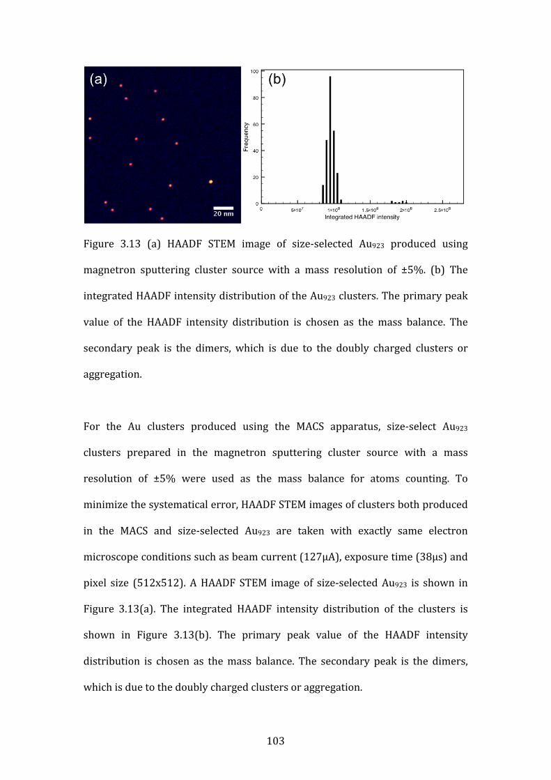
103
Figure 3.13 (a) HAADF STEM image of size-‐selected Au923 produced using
magnetron sputtering cluster source with a mass resolution of ±5%. (b) The
integrated HAADF intensity distribution of the Au923 clusters. The primary peak
value of the HAADF intensity distribution is chosen as the mass balance. The
secondary peak is the dimers, which is due to the doubly charged clusters or
aggregation.
For the Au clusters produced using the MACS apparatus, size-‐select Au923
clusters prepared in the magnetron sputtering cluster source with a mass
resolution of ±5% were used as the mass balance for atoms counting. To
minimize the systematical error, HAADF STEM images of clusters both produced
in the MACS and size-‐selected Au923 are taken with exactly same electron
microscope conditions such as beam current (127μA), exposure time (38μs) and
pixel size (512x512). A HAADF STEM image of size-‐selected Au923 is shown in
Figure 3.13(a). The integrated HAADF intensity distribution of the clusters is
shown in Figure 3.13(b). The primary peak value of the HAADF intensity
distribution is chosen as the mass balance. The secondary peak is the dimers,
which is due to the doubly charged clusters or aggregation.

104
105
List of references
[1] Pratontep, S., et al. "Size-‐selected cluster beam source based on radio
frequency magnetron plasma sputtering and gas condensation." Review of
scientific instruments 76.4 (2005): 045103.
[2] Smith, Roger. Atomic and ion collisions in solids and at surfaces: theory,
simulation and applications. Cambridge University Press, 2005.
[3] Haberland, Hellmut, et al. "Thin films from energetic cluster impact: a
feasibility study." Journal of Vacuum Science & Technology A 10.5 (1992): 3266-‐
3271.
[4] Hall, S. G., et al. "Compact sputter source for deposition of small size-‐selected
clusters." Review of scientific instruments 68.9 (1997): 3335-‐3339.
[5] Wucher, A., and M. Wahl. "The formation of clusters during ion induced
sputtering of metals." Nuclear Instruments and Methods in Physics Research
Section B: Beam Interactions with Materials and Atoms 115.1 (1996): 581-‐589.
[6] Granqvist, C. G., and R. A. Buhrman. "Ultrafine metal particles." Journal of
Applied Physics 47.5 (1976): 2200-‐2219.
[7] Olynick, D. L., J. M. Gibson, and R. S. Averback. "Impurity-‐suppressed sintering
in copper nanophase materials." Philosophical Magazine A 77.5 (1998): 1205-‐
1221.
[8] Soler, J. M., et al. "Microcluster growth: transition from successive monomer
addition to coagulation." Physical Review Letters 49.25 (1982): 1857.
[9] Hihara, Takehiko, and Kenji Sumiyama. "Formation and size control of a Ni
cluster by plasma gas condensation." Journal of applied physics 84.9 (1998):
5270-‐5276.
106
[10] Manura, David J., and David A. Dahl. "Simion Version 8.0/8.1 User Manual."
(2011).
[11] Von Issendorff, B., and R. E. Palmer. "A new high transmission infinite range
mass selector for cluster and nanoparticle beams." Review of Scientific
Instruments 70.12 (1999): 4497-‐4501.
[12] Wang, Z. W., et al. "Quantitative Z-‐contrast imaging in the scanning
transmission electron microscope with size-‐selected clusters." Physical Review B
84.7 (2011): 073408.
[13] Li, Z. Y., et al. "Three-‐dimensional atomic-‐scale structure of size-‐selected
gold nanoclusters." Nature 451.7174 (2008): 46-‐48.
[14] Young, N. P., et al. "Weighing supported nanoparticles: size-‐selected clusters
as mass standards in nanometrology." Physical review letters 101.24 (2008):
246103.
[15] Abràmoff, Michael D., Paulo J. Magalhães, and Sunanda J. Ram. "Image
processing with ImageJ." Biophotonics international 11.7 (2004): 36-‐42.
107
Chapter 4 Deposition of size-‐selected
gold nanoclusters
Two parts of works are included in this chapter with combined techniques of
cluster production using magnetron cluster source and characterization using
ac-‐STEM. In the first part, the size dependent propagation of clusters through
few-‐layer graphene (FLG) is explored. This work enables the control of
properties of graphene-‐based materials and other membranes, which have
potential in application of selective permeation filter. The second part
investigates the control of nanocluster structures (Au923) during the formation
stage in the gas phase. The breakthrough of this work offers a routine to study
the properties of clusters not only as a function of size but also isomer
configurations. It also provides possibility of production of isomerically pure
clusters for applications such as catalysis. Although the works presented in this
chapter reveal the vast potential of nanoclusters, the bridge connecting the
fundamental demonstration and the applications is, we believe, abundant
production. This is our motivation to develop the matrix assembly cluster source,
which will be discussed in Chapter 5 and Chapter 6.
108
The works presented in this chapter are the results of collaboration between the
author and co-‐supervisor, Dr. Simon Plant. The ideas of these two experiments
were both from Dr. Simon Plant. The sample preparation was done by Dr. Simon
Plant. Sample characterization using ac-‐STEM was done by the author. Data
analysis and discussion were contributed by both the author and Dr. Simon
Plant. The two parts of works were published on Nanoscale [1] and JACS [2]
respectively.
4.1 Size-‐dependent propagation
4.1.1 Overview
Through the development of cluster ion beam technology and the mass selection
technique, highly controlled deposition of clusters is achieved not only for size
but as well as for surface coverage and deposition energy [3-‐4]. This has enabled
the interactions between nanoclusters and the substrates surface to be carefully
analysed, which in turn promotes the development of novel materials with
applications on a variety of areas [5-‐6].
Deposition of nanoclusters onto graphene offers a way to alter and tailor their
properties, which also enables one to explore the interaction between
nanoclusters and the graphene’s surface as previously reported of size selected
Pd nanoclusters deposited on supported graphene [7-‐8]. The interaction
between metals and graphene is a cutting-‐edge topic because of the increasing
interests on metal-‐graphene composite materials and the promising properties
109
of metal on graphene based electronics [9-‐10]. Gold as model metal cluster
deposited on graphene via solution or coating has been studied intensively in
last few years using electron microscope especially on its behavior or dynamics
on the graphene film [11-‐15]. Researches have demonstrated the enhanced
chemical sensitivity of graphene decorated with metal nanoclusters, which has
potential applications such as sensing [16-‐18].
In this work, Au nanoclusters with two different sizes are deposited onto few
layer graphene (FLG) surface under specific deposition energy to demonstrate
the size dependent propagation through few layer graphene, via the mechanism
of defect generation. Although the graphene membrane is atomically thin and it
is impermeable, its properties can be tuned and could be used as a selectively
permeable membrane after the defect generation by size selected nanoclusters
[19-‐21]. In previous work, defect generation by size selected nanoclusters have
been reported to decorate nanoporous membrane which is similar to atomic ion
bombardment of graphene [22-‐23]. Also the deposition of size selected Ag
nanoclusters from 3 to 5000 atoms on graphite has been investigated intensively
[24-‐36]. Here, size selected Au55 nanoclusters was used to bombard graphite
surface first to create defects in order to determine the implantation depth of
nanoclusters under specific deposition energy using scanning tunneling
microscope (STM). This technique is then transferred to suspended FLG film and
use aberration corrected scanning transmission electron microscope (ac-‐STEM)
to track the fates of deposited Au55 and Au923 clusters.
110
4.1.2 Sample preparation and implantation depth of nanoclusters into
graphite
The size selected Au nanoclusters are prepared in the magnetron sputtering gas
condensation cluster source as introduced previously. The size of clusters is
selected by the lateral time-‐of-‐flight mass selector prior to the deposition onto
the substrate. The mass resolution used for both Au55 and Au923 are M/ΔM=20,
which is determined by the exit aperture size of the mass filter [37-‐39]. The
deposition energy of clusters is controlled by the bias voltage applied on the
substrate. The coverage of nanoclusters on the substrate is monitored by the
beam current and the integrated deposition time. Size selected Au55
nanoclusters are first produced to study the implantation depth of nanoclusters
into the highly ordered pyrolytic graphite (HOPG, grade ZYB). The surface of the
HOPG is freshly cleaved and the deposition energy of the Au55 nanoclusters is
5keV determined by the bias voltage on the substrate. After deposition the HOPG
is transferred to the tube furnace immediately after removal from vacuum
chamber, where the HOPG is etched oxidatively at 650°C for 3mins in ambient
atmosphere to widen the nanoscale implantation channels laterally created by
the nanoclusters, which are reactive to oxygen, enable to be measured by the
STM tip. While the depth of the channels remain the same as the bottom is defect
free. The etch pits are then analyzed in bench top STM (Veeco Digital
Instruments Nanoscope IIIa) in ambient atmosphere to obtain the implantation
depth. A mechanically cut Pt/Ir wire is used as STM tip and typical tunneling
parameters we used are 0.5V bias voltage on the tip and tunneling current of
0.5nA.
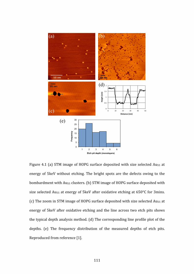
111
Figure 4.1 (a) STM image of HOPG surface deposited with size selected Au55 at
energy of 5keV without etching. The bright spots are the defects owing to the
bombardment with Au55 clusters. (b) STM image of HOPG surface deposited with
size selected Au55 at energy of 5keV after oxidative etching at 650°C for 3mins.
(c) The zoom in STM image of HOPG surface deposited with size selected Au55 at
energy of 5keV after oxidative etching and the line across two etch pits shows
the typical depth analysis method. (d) The corresponding line profile plot of the
depths. (e) The frequency distribution of the measured depths of etch pits.
Reproduced from reference [1].
0"
0.5"
1"
1.5"
2"
0" 10" 20" 30" 40" 50"
Height'(n
m)'
Distance'(nm)'
(a)" (b)"
(c)"
(d)"
0
5
10
15
20
25
30
1 2 3 4 5 6
Freq
uenc
y
Etch pit depth (monolayers)
(e)"
112
The STM images of HOPG surface with implantation of Au55 at 5keV are shown in
Figure 4.1. Figure 4.1(a) is the STM image of HOPG surface implanted by size
selected Au55 nanoclusters at 5keV but without oxidative etching. The bright
spots are the defects on the graphite lattice created by clusters land on the
surface. However, as diameter of Au55 is less than 1nm, the defects owing to Au55
nanocluster implantation is too narrow to be measured by the STM tip in
ambient atmosphere. Therefore the oxidative etching is a necessity to widen the
nanoscale channels laterally to enable the STM measurement. The STM image of
HOPG after Au55 implantation and after oxidative etching is shown in Figure
4.1(b). The depth of resultant each etch pit is measured by a line profile plot, as
shown in Figure 4.1(c) and 4.1(d), to obtain the depth distribution as shown in
Figure 4.1(e).
The histogram of depth distribution shown in Figure 4.1(e) does not represent
the actual implantation depth of nanoclusters into graphite [38]. Although the
defects created by clusters implantation expand laterally during oxidative
etching, the lattice damage is also partially healed when annealing the HOPG at
high temperature [32]. The final depth of the resultant etch pits is the dynamic
competition between the oxidative etching and the thermal annealing that
reducing the depth of many etch pits, which have been investigated previously
by Ag cluster implanted into graphite with MD simulations. The results indicate
the maximum depth of resultant etch pits gives the nanocluster implantation
depth which is 6 layers for Au55 with implantation energy of 5keV, which means
the Au55 nanoclusters deposited at 5keV is able to penetrate 6 monolayers
graphene film. This number consists well with the previously measured pinning
113
energy threshold, the required energy to make a point defect on a single
monolayer graphite lattice, which is 0.75keV for Au55 [41-‐42]. Extrapolated from
the pinning energy, the implantation depth is equivalent to 6.7 layers where the
error is within 1 monolayer from experimental results.
4.1.3 Controlled deposition of size selected Au55 and Au923 on FLG
The few layer graphene (FLG) film used in this work is grown by CVD with an
average thickness of the FLG is 4 monolayers suspended on Cu TEM grid (from
Graphene Laboratories Inc.). Size selected Au55 nanoclusters are produced in
magnetron sputtering cluster source and deposited on the FLG with deposition
energy of 5keV. The FLG deposited with Au55 nanoclusters is studied in the
aberration-‐corrected scanning transmission electron microscope (STEM). Both
bright field (BF) and high angle annular dark field (HAADF) images are taken to
examine the FLG as well as the deposited clusters. The STEM image reveals the
thickness of the FLG film varies across the surface. Also hydrocarbons coating is
observed on the FLG surface from STEM images that might affect the interaction
between Au cluster and the FLG surface. Depositing nanoclusters onto
hydrocarbon-‐based surface have been studied previously both for grahene
produced by micromechanical exfoliation (pristine graphene) and CVD growth
[11-‐12]. As indicated in those studies e.g. evaporating Au atoms onto graphene,
Au atoms cannot bond to clean graphene monolayer that they are observed as
single atoms or only aggregate around surface hydrocarbons, although Au bond
to clean few layer graphene surface has been reported [11-‐12].
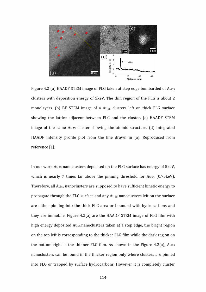
114
Figure 4.2 (a) HAADF STEM image of FLG taken at step edge bombarded of Au55
clusters with deposition energy of 5keV. The thin region of the FLG is about 2
monolayers. (b) BF STEM image of a Au55 clusters left on thick FLG surface
showing the lattice adjacent between FLG and the cluster. (c) HAADF STEM
image of the same Au55 cluster showing the atomic structure. (d) Integrated
HAADF intensity profile plot from the line drawn in (a). Reproduced from
reference [1].
In our work Au55 nanoclusters deposited on the FLG surface has energy of 5keV,
which is nearly 7 times far above the pinning threshold for Au55 (0.75keV).
Therefore, all Au55 nanoclusters are supposed to have sufficient kinetic energy to
propagate through the FLG surface and any Au55 nanoclusters left on the surface
are either pinning into the thick FLG area or bounded with hydrocarbons and
they are immobile. Figure 4.2(a) are the HAADF STEM image of FLG film with
high energy deposited Au55 nanoclusters taken at a step edge, the bright region
on the top left is corresponding to the thicker FLG film while the dark region on
the bottom right is the thinner FLG film. As shown in the Figure 4.2(a), Au55
nanoclusters can be found in the thicker region only where clusters are pinned
into FLG or trapped by surface hydrocarbons. However it is completely cluster
(b)! (c)!
(a)!
(d)!
0!
1!
2!
3!
4!
0! 20! 40! 60!
Intensity
((a.(u
.)(
Distance (nm)
Au55!
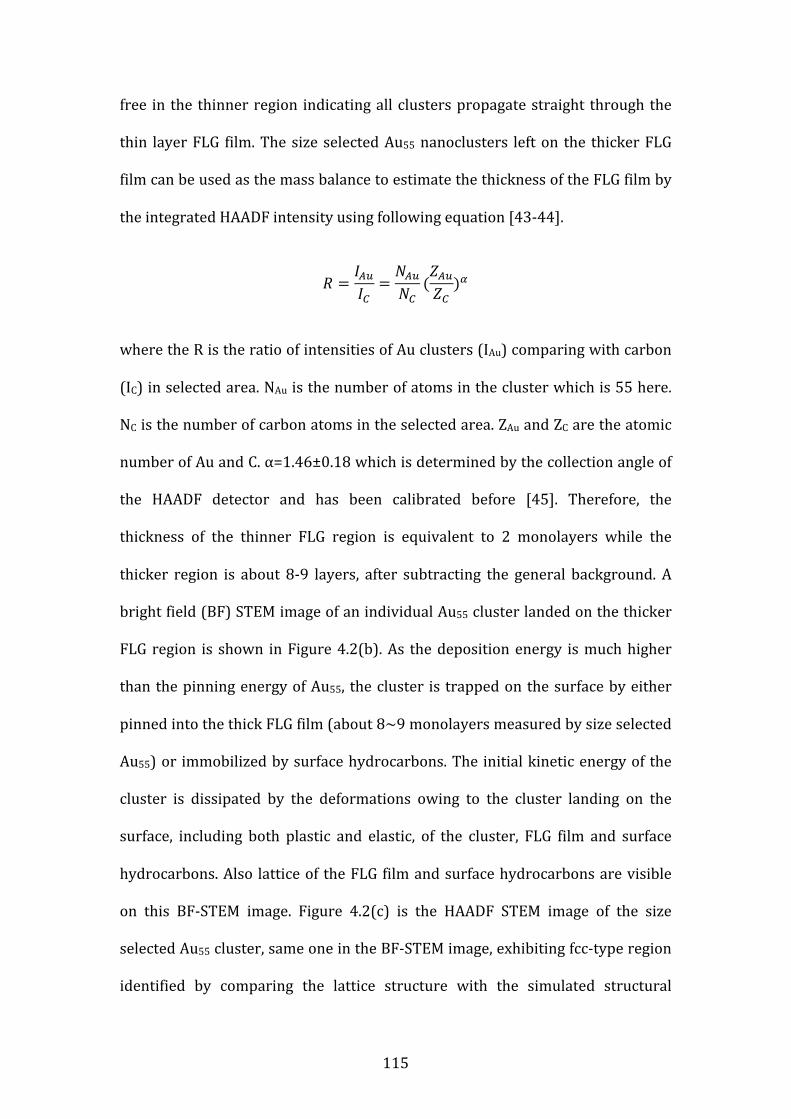
115
free in the thinner region indicating all clusters propagate straight through the
thin layer FLG film. The size selected Au55 nanoclusters left on the thicker FLG
film can be used as the mass balance to estimate the thickness of the FLG film by
the integrated HAADF intensity using following equation [43-‐44].
𝑅 =𝐼!"𝐼!=𝑁!"𝑁!
(𝑍!"𝑍!)!
where the R is the ratio of intensities of Au clusters (IAu) comparing with carbon
(IC) in selected area. NAu is the number of atoms in the cluster which is 55 here.
NC is the number of carbon atoms in the selected area. ZAu and ZC are the atomic
number of Au and C. α=1.46±0.18 which is determined by the collection angle of
the HAADF detector and has been calibrated before [45]. Therefore, the
thickness of the thinner FLG region is equivalent to 2 monolayers while the
thicker region is about 8-‐9 layers, after subtracting the general background. A
bright field (BF) STEM image of an individual Au55 cluster landed on the thicker
FLG region is shown in Figure 4.2(b). As the deposition energy is much higher
than the pinning energy of Au55, the cluster is trapped on the surface by either
pinned into the thick FLG film (about 8~9 monolayers measured by size selected
Au55) or immobilized by surface hydrocarbons. The initial kinetic energy of the
cluster is dissipated by the deformations owing to the cluster landing on the
surface, including both plastic and elastic, of the cluster, FLG film and surface
hydrocarbons. Also lattice of the FLG film and surface hydrocarbons are visible
on this BF-‐STEM image. Figure 4.2(c) is the HAADF STEM image of the size
selected Au55 cluster, same one in the BF-‐STEM image, exhibiting fcc-‐type region
identified by comparing the lattice structure with the simulated structural

116
isomers [46]. The observed high symmetry structure of the cluster indicating
there is no fragmentation when the cluster landed on the surface suggesting the
landing process of the cluster is buffered by the surface hydrocarbons which
work as a breaking cushion [47]. However, the FLG lattice is not visible in the
HAADF STEM image as the contrast of the HAADF image is a function of atomic
number. Figure 4.2(d) is the intensity plot of the line profile drawn in Figure
4.2(a) perpendicular to the step edge of the thick and thin FLG film regions and
across a Au55 cluster which is corresponding to the sharp spark in the plot.
Figure 4.3 (a) HAADF STEM image of FLG taken at step edge bombarded of both
size selected Au55 and Au923 clusters with deposition energy of 5keV. The thinner
region of the FLG is about 3-‐4 monolayers and only Au923 clusters reside there.
Au55 clusters are marked with red arrow in the thicker region. (b) HAADF STEM
image of thinner FLG region (about 4 monolayers) showing Au923 clusters are
(c)! (d)!
(a)!
Au55!
Au55!Au923!
(b)!
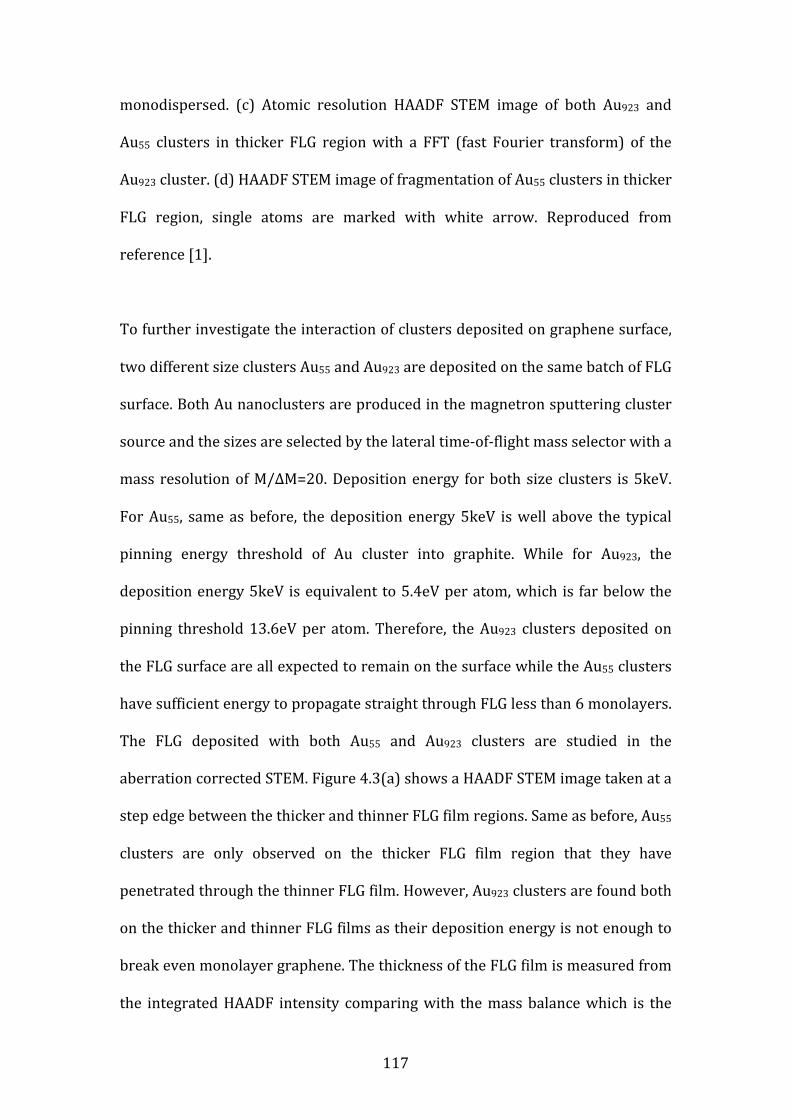
117
monodispersed. (c) Atomic resolution HAADF STEM image of both Au923 and
Au55 clusters in thicker FLG region with a FFT (fast Fourier transform) of the
Au923 cluster. (d) HAADF STEM image of fragmentation of Au55 clusters in thicker
FLG region, single atoms are marked with white arrow. Reproduced from
reference [1].
To further investigate the interaction of clusters deposited on graphene surface,
two different size clusters Au55 and Au923 are deposited on the same batch of FLG
surface. Both Au nanoclusters are produced in the magnetron sputtering cluster
source and the sizes are selected by the lateral time-‐of-‐flight mass selector with a
mass resolution of M/ΔM=20. Deposition energy for both size clusters is 5keV.
For Au55, same as before, the deposition energy 5keV is well above the typical
pinning energy threshold of Au cluster into graphite. While for Au923, the
deposition energy 5keV is equivalent to 5.4eV per atom, which is far below the
pinning threshold 13.6eV per atom. Therefore, the Au923 clusters deposited on
the FLG surface are all expected to remain on the surface while the Au55 clusters
have sufficient energy to propagate straight through FLG less than 6 monolayers.
The FLG deposited with both Au55 and Au923 clusters are studied in the
aberration corrected STEM. Figure 4.3(a) shows a HAADF STEM image taken at a
step edge between the thicker and thinner FLG film regions. Same as before, Au55
clusters are only observed on the thicker FLG film region that they have
penetrated through the thinner FLG film. However, Au923 clusters are found both
on the thicker and thinner FLG films as their deposition energy is not enough to
break even monolayer graphene. The thickness of the FLG film is measured from
the integrated HAADF intensity comparing with the mass balance which is the
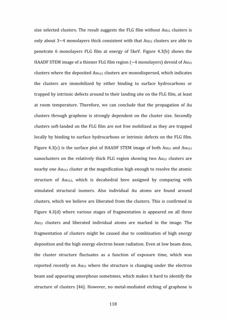
118
size selected clusters. The result suggests the FLG film without Au55 clusters is
only about 3~4 monolayers thick consistent with that Au55 clusters are able to
penetrate 6 monolayers FLG film at energy of 5keV. Figure 4.3(b) shows the
HAADF STEM image of a thinner FLG film region (~4 monolayers) devoid of Au55
clusters where the deposited Au923 clusters are monodispersed, which indicates
the clusters are immobilized by either binding to surface hydrocarbons or
trapped by intrinsic defects around to their landing site on the FLG film, at least
at room temperature. Therefore, we can conclude that the propagation of Au
clusters through graphene is strongly dependent on the cluster size. Secondly
clusters soft-‐landed on the FLG film are not free mobilized as they are trapped
locally by binding to surface hydrocarbons or intrinsic defects on the FLG film.
Figure 4.3(c) is the surface plot of HAADF STEM image of both Au55 and Au923
nanoclusters on the relatively thick FLG region showing two Au55 clusters are
nearby one Au923 cluster at the magnification high enough to resolve the atomic
structure of Au923, which is decahedral here assigned by comparing with
simulated structural isomers. Also individual Au atoms are found around
clusters, which we believe are liberated from the clusters. This is confirmed in
Figure 4.3(d) where various stages of fragmentation is appeared on all three
Au55 clusters and liberated individual atoms are marked in the image. The
fragmentation of clusters might be caused due to combination of high energy
deposition and the high energy electron beam radiation. Even at low beam dose,
the cluster structure fluctuates as a function of exposure time, which was
reported recently on Au55 where the structure is changing under the electron
beam and appearing amorphous sometimes, which makes it hard to identify the
structure of clusters [46]. However, no metal-‐mediated etching of graphene is
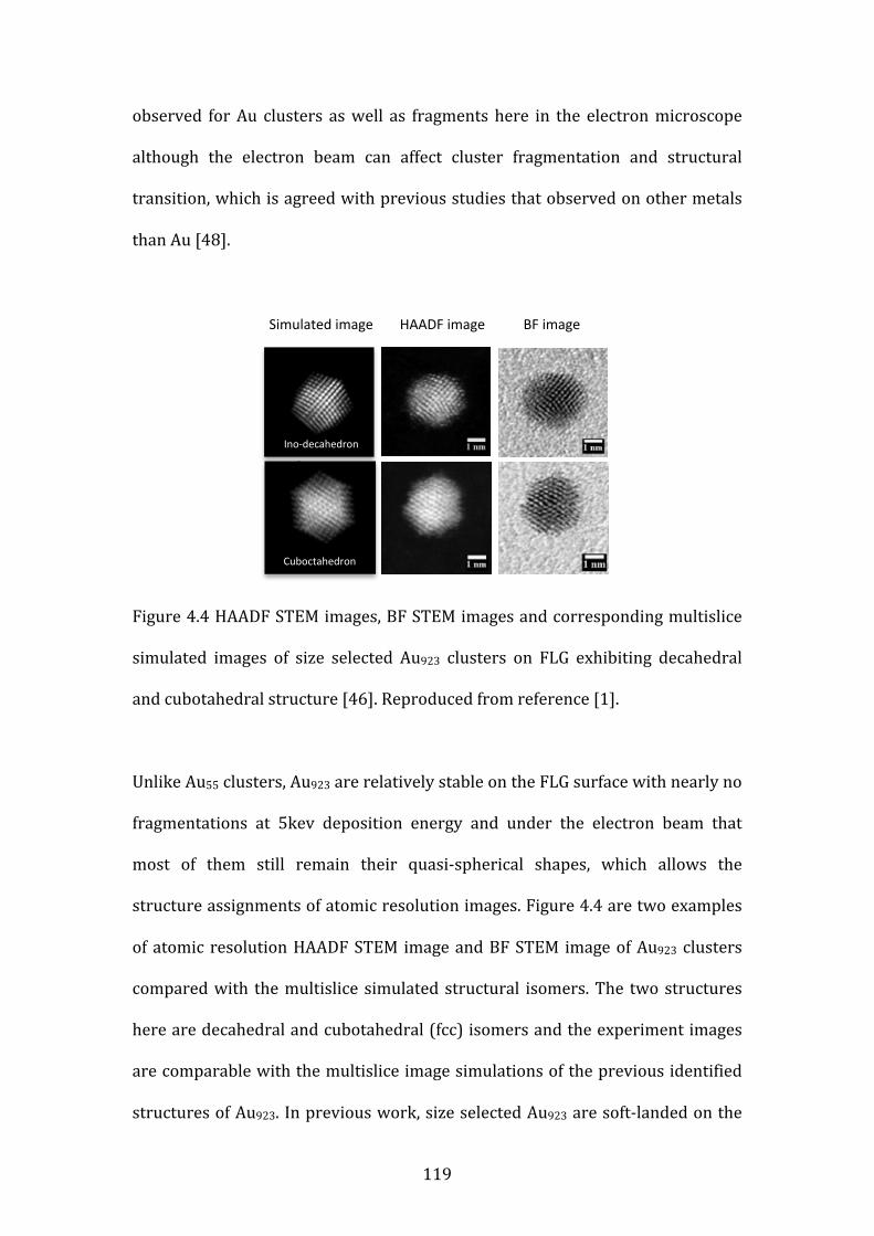
119
observed for Au clusters as well as fragments here in the electron microscope
although the electron beam can affect cluster fragmentation and structural
transition, which is agreed with previous studies that observed on other metals
than Au [48].
Figure 4.4 HAADF STEM images, BF STEM images and corresponding multislice
simulated images of size selected Au923 clusters on FLG exhibiting decahedral
and cubotahedral structure [46]. Reproduced from reference [1].
Unlike Au55 clusters, Au923 are relatively stable on the FLG surface with nearly no
fragmentations at 5kev deposition energy and under the electron beam that
most of them still remain their quasi-‐spherical shapes, which allows the
structure assignments of atomic resolution images. Figure 4.4 are two examples
of atomic resolution HAADF STEM image and BF STEM image of Au923 clusters
compared with the multislice simulated structural isomers. The two structures
here are decahedral and cubotahedral (fcc) isomers and the experiment images
are comparable with the multislice image simulations of the previous identified
structures of Au923. In previous work, size selected Au923 are soft-‐landed on the
!!
!!
Simulated!image! HAADF!image!
Ino3decahedron!
Cuboctahedron!
BF!image!
120
amorphous carbon film and the deposition energy is only 0.5eV per atom [49]. In
our current work, the deposition energy of Au923 is 5.4eV per atom but it doesn’t
affect or fragment the clusters. The comparison between atomic resolution
HAADF STEM image and multislice simulated image has been widely used on the
structure identification of many other clusters such as Au20 and Au55.
The remaining challenge of this work is the defects on the thinner FLG film
region (less then 6 monolayers) induced by Au55 penetration are not visualized
in our aberration corrected STEM. But we believe it might be achieved in the
future by using the low energy aberration corrected HAADF STEM, such as
60keV, to avoid electron beam damage on the FLG film [50].
4.1.4 Conclusion
In summary, in this work the size dependent propagation of highly controlled
nanoclusters through FLG have been demonstrated, using the cluster ion beam
deposition technique combined with the magnetron sputtering and lateral time-‐
of-‐flight mass selection. At the same deposition energy, Au55 nanoclusters are
found to penetrate through the thin FLG film via mechanism of defect generation,
while Au923 nanoclusters are left on the surface and monodisperse. This work
opens the way to use nanolcusters to induce controlled defects on graphene film
as well as controlled nanoclusters, which is greatly advantageous for the
development of graphene based functional materials.
121
4.2 Atomic structure control
4.2.1 Overview
Nanoclusters, especially for Au nanoclusters, are reported to attract considerable
attentions and be used extensively in many areas such as catalyst,
nanoelectronics as well as plasmonics due to their strongly size and structure
dependent properties [49-‐59]. The cluster ion beam deposition technology
combined with mass selector, e.g. the lateral time-‐of-‐flight mass selector and
Quadrapole, enables the controlled production of nanoclusters with specific size,
composition, surface coverage and deposition energy and permits the
investigation of the size dependent properties of nanoclusters [2-‐4]. However,
even for a specific size nanoclusters exhibit various atomic configurations as
previously studied on small gold nanoclusters Au20, Au55 and large gold
nanoclusters such as Au309 and Au923 [44-‐46,49]. The structural control of the
nanoclusters down to the atomic level still remains a challenge.
Since the atomic configurations of nanoclusters play important roles on their
active sites which is critical for applications such as catalyst, it would be great
advantageous to control their isomer populations at the formation stage, which
enables the control of the properties of nanoclusters. Here, we are reporting the
routine which is able to control the atomic structures of size selected Au
nanoclusters during the formation by tuning the parameters in magnetron
sputtering gas condensation cluster beam source. This method has been used in
the magnetron sputtering cluster source before to transfer the core-‐shell
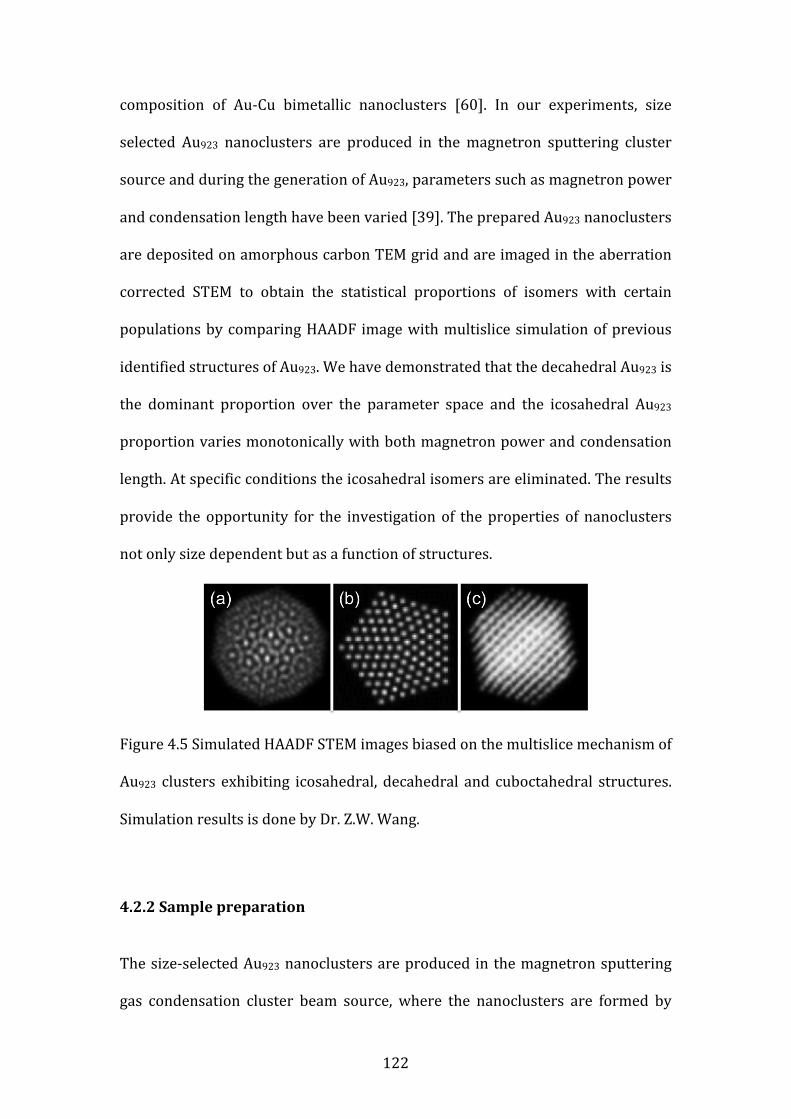
122
composition of Au-‐Cu bimetallic nanoclusters [60]. In our experiments, size
selected Au923 nanoclusters are produced in the magnetron sputtering cluster
source and during the generation of Au923, parameters such as magnetron power
and condensation length have been varied [39]. The prepared Au923 nanoclusters
are deposited on amorphous carbon TEM grid and are imaged in the aberration
corrected STEM to obtain the statistical proportions of isomers with certain
populations by comparing HAADF image with multislice simulation of previous
identified structures of Au923. We have demonstrated that the decahedral Au923 is
the dominant proportion over the parameter space and the icosahedral Au923
proportion varies monotonically with both magnetron power and condensation
length. At specific conditions the icosahedral isomers are eliminated. The results
provide the opportunity for the investigation of the properties of nanoclusters
not only size dependent but as a function of structures.
Figure 4.5 Simulated HAADF STEM images biased on the multislice mechanism of
Au923 clusters exhibiting icosahedral, decahedral and cuboctahedral structures.
Simulation results is done by Dr. Z.W. Wang.
4.2.2 Sample preparation
The size-‐selected Au923 nanoclusters are produced in the magnetron sputtering
gas condensation cluster beam source, where the nanoclusters are formed by
123
supersaturated atomic vapor condensed in rare gas atmosphere and the size of
the nanoclusters is selected by the inline lateral time-‐of-‐flight mass filter using a
mass resolution of M/ΔM=20, which is determined by the exit aperture size of
the mass filter. Therefore, the size selected Au923 nanoclusters actually contain
923±23 atoms [39]. To explore effects of preparation conditions on cluster
atomic structure, parameters such as magnetron power, condensation length, Ar
and He gas flow and gas pressure in the condensation chamber are varied during
the generation of the nanoclusters. All nanoclusters prepared in the magnetron
source are soft-‐landed on the amorphous carbon film TEM grid to retain their
free space structures, insofar as possible. The deposition energy used is 1.5keV
equivalent to 1.6eV per atom controlled by the bias voltage applied on the
sample holder, which is well below the typical pinning energy threshold of Au
cluster onto graphite (~14eV per atom) [41]. Clusters are then characterized in
the aberration-‐corrected STEM, JEOL 2100F, equipped with the 200keV electron
beam and HAADF detector (62 mrad collection angle). The structure of clusters
are assigned by comparing the HAADF images with the multislice simulated
HAADF-‐STEM images from previously identified atomic structures of Au923 as
shown in Figure 4.5 (The simulation is done by Dr. Z.W. Wang). The statistical
proportions of structural isomers at each experimental condition are obtained by
the structural analysis of more than 1200 clusters.
The previous identified high symmetry structures of Au923 nanocluster are the
icosahedral (Ih), decahedral (Dh) and cuboctahedral (fcc) [49]. The structural
models of these three high symmetry isomers are shown in Figure 4.6(a-‐c). The
corresponding HAADF STEM images of Au923 nanoclusters represent the Ih, Dh
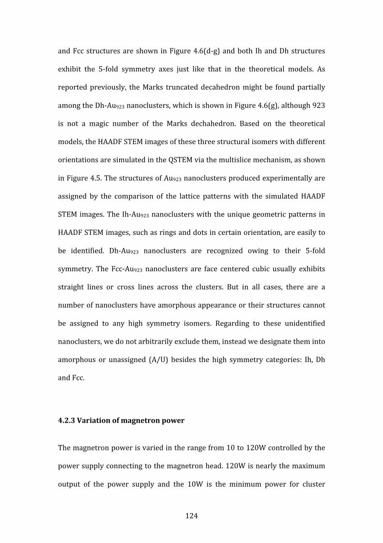
124
and Fcc structures are shown in Figure 4.6(d-‐g) and both Ih and Dh structures
exhibit the 5-‐fold symmetry axes just like that in the theoretical models. As
reported previously, the Marks truncated decahedron might be found partially
among the Dh-‐Au923 nanoclusters, which is shown in Figure 4.6(g), although 923
is not a magic number of the Marks dechahedron. Based on the theoretical
models, the HAADF STEM images of these three structural isomers with different
orientations are simulated in the QSTEM via the multislice mechanism, as shown
in Figure 4.5. The structures of Au923 nanoclusters produced experimentally are
assigned by the comparison of the lattice patterns with the simulated HAADF
STEM images. The Ih-‐Au923 nanoclusters with the unique geometric patterns in
HAADF STEM images, such as rings and dots in certain orientation, are easily to
be identified. Dh-‐Au923 nanoclusters are recognized owing to their 5-‐fold
symmetry. The Fcc-‐Au923 nanoclusters are face centered cubic usually exhibits
straight lines or cross lines across the clusters. But in all cases, there are a
number of nanoclusters have amorphous appearance or their structures cannot
be assigned to any high symmetry isomers. Regarding to these unidentified
nanoclusters, we do not arbitrarily exclude them, instead we designate them into
amorphous or unassigned (A/U) besides the high symmetry categories: Ih, Dh
and Fcc.
4.2.3 Variation of magnetron power
The magnetron power is varied in the range from 10 to 120W controlled by the
power supply connecting to the magnetron head. 120W is nearly the maximum
output of the power supply and the 10W is the minimum power for cluster
125
generation (plasma is hard to be ignited if power is less than 10W). The role of
the magnetron power is to control the sputtering yield of the target, which is
gold here, to produce supersaturated atomic vapor for cluster formation. The
proportions of isomers of nanoclusters observed with certain population are
plotted in Figure 4.6(h) as a function of the increasing magnetron power. The
initial (lowest magnetron power) and final (highest magnetron power) states of
proportions of all four categories are highlighted in Figure 4.6(I). The deposition
energy used for the Au923 nanoclusters is 1.5keV equivalent to 1.6eV per atom,
which is far below the typical pinning energy threshold of Au into graphite
(about 14eV per atom). In previously reported studies on structures of Au923
nanocluters, the deposition energy used is 0.5eV/atom depositing on amorphous
carbon film and 5.4eV/atom depositing on FLG film respectively. As shown in
Figure 4.6(h-‐I), the Dh-‐Au923 isomer is founded to be the most abundant
proportion over all different magnetron powers. The proportions of Fcc-‐Au923
and the A/U are not varied significantly across the parameter space. These
results are agreed well with the predictions reported by Li et al. stating in spite
of the fact that Ih isomer is more favored than Dh or Fcc in small clusters, which
contain less than 100 atoms, the Ino-‐Dh is the most stable structure for large
clusters up to 1000 atoms [61]. Experiments by Koga et al. have also shown Au
nanoparticles with diameter of 3nm (similar to the size of Au923) are initially
icosahedral majored when produced in the gas phase by rapid condensation of
atomic vapor but vast majority of them are converted to Dh by thermal annealing
[62]. Therefore, in our case for Au923 nanoclusters the Dh isomer is more likely to
be the most equilibrium structure. In our present results, the proportion of Dh-‐
Au923 is observed decreasing monotonically (gradient -‐0.09, R2>0.99) with the
126
increasing magnetron power while the proportion of Ih-‐Au923 raises up (gradient
0.12, R2=0.99), which reflects the Dh-‐Au923 is competing with the Ih-‐Au923.
Figure 4.6 (a) Geometry models of icosahedral structure of Au923. (b) Geometry
models of cuboctahedral (fcc) structure of Au923. (c) Geometry models of Ino-‐
decahedral structure of Au923. (d) HAADF STEM image of Au923 exhibiting
icosahedral isomer. (e) HAADF STEM image of Au923 showing cuboctahedral
isomer. (f) HAADF STEM image of Au923 exhibiting decahedral structure. (g)
Decahedral Au923 clusters exhibiting Marks decahedron. (h) Proportions of Ih,
Dh, fcc and A/U isomers within certain population of Au923 clusters prepared
with different magnetron power. (i) The proportions of the four compositions at
the lowest and highest magnetron power. Reproduced from reference [2].
0
10
20
30
40
0 25 50 75 100 125
Pop
ulat
ion
(%)
Magnetron power (W)
Ih Dh fcc A/U
h) i) Initial (10 W)
Final (120 W)
Ih 8%
Dh 39% fcc
27%
A/U 26%
Ih 22%
Dh 29%
fcc 25%
A/U 24%
d) f) g) e)
a) b) c)
End view
Side view
127
The internal competition between Dh and Ih isomers leads us to consider the
nanocluster formation mechanism microscopically down to the atomic level. The
results show the Ih isomers are more favored with higher magnetron power
where the atomic vapor is more supersaturated. Based on previous studies, the
metastable icosahedra observed in large nanoclusters might be attributed to the
kinetic trapping effect, where the large Ih nanoclusters grow on top of small Ih
nanoclusters, which is just like the seeds through the completion of the out-‐layer
geometry shells [51,62-‐63]. This is also confirmed in theory by molecular
dynamics (MD) simulations, which suggests the icosahedral isomers are
dominated in the ideal atom-‐wise growth, while the coalescence prefers to
produce Dh and Fcc isomers [64]. In the magnetron sputtering gas condensation
cluster source, the supersaturated atomic vapor is more dense with increasing
magnetron power. The higher density of Au atoms leads to more rapid growth of
nanoclusters also driving the states of nanoclusters further away from
equilibrium. The Fcc structures are possibly determined by the thermodynamic
effect, therefore the proportion of Fcc-‐Au923 nanoclusters is less varied across
the parameter space.
4.2.4 Variation of condensation length
The condensation length in the magnetron sputtering gas condensation cluster
source is the distance between the magnetron head and the nozzle exit of the
condensation chamber. The condensation chamber is the inner chamber inside
the generation chamber in the cluster source, which is usually hollow and can be
cooled by liquid nitrogen. A nozzle is mounted on the end of the condensation
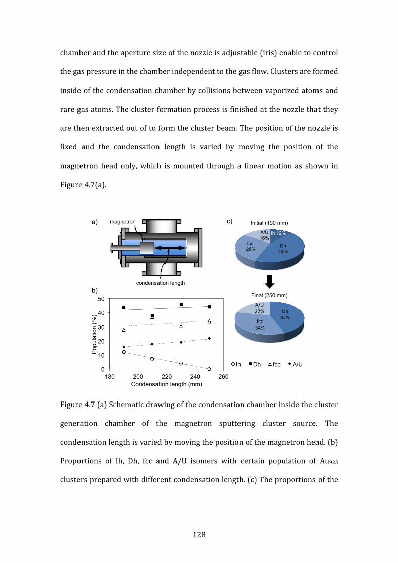
128
chamber and the aperture size of the nozzle is adjustable (iris) enable to control
the gas pressure in the chamber independent to the gas flow. Clusters are formed
inside of the condensation chamber by collisions between vaporized atoms and
rare gas atoms. The cluster formation process is finished at the nozzle that they
are then extracted out of to form the cluster beam. The position of the nozzle is
fixed and the condensation length is varied by moving the position of the
magnetron head only, which is mounted through a linear motion as shown in
Figure 4.7(a).
Figure 4.7 (a) Schematic drawing of the condensation chamber inside the cluster
generation chamber of the magnetron sputtering cluster source. The
condensation length is varied by moving the position of the magnetron head. (b)
Proportions of Ih, Dh, fcc and A/U isomers with certain population of Au923
clusters prepared with different condensation length. (c) The proportions of the
0
10
20
30
40
50
180 200 220 240 260
Pop
ulat
ion
(%)
Condensation length (mm)
Ih Dh fcc A/U
a) c) Initial (190 mm)
Final (250 mm) b)
Ih 12%
Dh 44%
fcc 28%
A/U 16%
Dh#44%#
fcc#34%#
A/U#22%#
magnetron
condensation length
129
four compositions at the shortest and longest condensation length. Reproduced
from reference [2].
Similar to the different magnetron power, the relative proportions of all three
high symmetry isomers, Ih, Dh and Fcc as well as the unidentified category (A/U)
within certain populations are plotted as a function of the increasing
condensation length from 190 to 250mm as shown in Figure 4.7(b). The
magnetron power used here is settled at the lowest 10W. All other parameters
remain the same as preparing clusters with different magnetron power in last
section, except for there is a difference of 0.04mbar on the pressure of the
condensation chamber. This difference might be the reason cause the shifts
among the proportions of Ih, Dh and fcc isomers between the two data sets
where all other parameters are exactly identical (10W magnetron power and
250mm condensation length in Figure). Similar to the results in the different
magnetron power, the Dh-‐Au923 isomers are still the most abundant proportion
here near 40% over parameters range, following by the Fcc structures around
30% and the Ih isomers are the least only 10%. The proportions of all four
categories at initial (shortest condensation length) and final (longest
condensation length) states are highlighted in Figure 4.7(c). As shown in Figure
4.7(b), the Ih-‐Au923 proportion is declined significantly (gradient -‐0.20, R2=0.99)
as a function of increasing condensation length and the Ih-‐Au923 isomers are
completely devoid at the longest condensation length 250mm. However, both Dh
isomers and Fcc isomers are increased with the increasing condensation length
and the trend indicates there is interplay between each other. With a fixed
magnetron power, the average concentration of the atomic vapor inside the
130
condensation chamber is defined by the volume of the chamber so that it varies
as 1/L (L is the condensation length as the volume of the chamber is bounded by
the walls and the magnetron head). The mean free path inside the condensation
chamber is indeed increased with longer condensation length resulting slower
nanocluster growth prior to be extracted out of the condensation chamber
through the nozzle. With increasing condensation length, the reaction kinetics
move more toward equilibrium and the kinetic trapping effect is reduced.
Therefore, higher proportions of equilibrium structures such as Dh and Fcc are
observed.
4.2.5 Conclusion
In summary, in this work we combined the atomic resolution HAADF-‐STEM
images with simulated HAADF-‐STEM image based on multislice mechanism for
the assignment of structures of Au923 nanoclusters to obtain the statistical
proportions of isomers within certain populations as a function of the
parameters (magnetron power and condensation length) used during
nanocluster generation stage. We have confirmed that the parameters used
during the nanoclusters formation have effects on the structures and moreover
we have demonstrated that the atomic structures of nanoclusters can be tuned
by controlling the formation parameters. The icosahedral isomers have been
found to follow a monotonic relationship as a function of both magnetron power
and condensation length over the parameters space, which provides us the
possibility to eliminate all the icosahedral isomers using specific parameters
setting during nanoclusters formation. With parameters setting for the

131
nonequilibrium conditions, there is found to be a interplay between icosahedral
and decahedral isomers which both exhibit the 5-‐fold symmetry axes, where
proportion of icosahedral isomers is favored from sacrifice of the decahedron.
This approach we presented here might have the potential to produce
nanoclusters which are isomerically pure and that will enable us to explore the
properties of nanoclusters not only as a function of size but atomic structural
dependence.
132
List of references
[1] Plant, Simon R., et al. "Size-‐dependent propagation of Au nanoclusters
through few-‐layer graphene." Nanoscale 6.3 (2014): 1258-‐1263.
[2] Plant, Simon R., Lu Cao, and Richard E. Palmer. "Atomic structure control of
size-‐selected gold nanoclusters during formation." Journal of the American
Chemical Society 136.21 (2014): 7559-‐7562.
[3] Palmer, R. E., S. Pratontep, and H-‐G. Boyen. "Nanostructured surfaces from
size-‐selected clusters." Nature Materials 2.7 (2003): 443-‐448.
[4] Bromann, Karsten, et al. "Controlled deposition of size-‐selected silver
nanoclusters." Science 274.5289 (1996): 956-‐958.
[5] Popok, Vladimir N., et al. "Cluster–surface interaction: From soft landing to
implantation." Surface Science Reports 66.10 (2011): 347-‐377.
[6] Claridge, Shelley A., et al. "Cluster-‐assembled materials." ACS nano 3.2 (2009):
244-‐255.
[7] Wang, Hongtao, et al. "Doping monolayer graphene with single atom
substitutions." Nano letters 12.1 (2011): 141-‐144.
[8] Wang, Bo, et al. "Size-‐selected monodisperse nanoclusters on supported
graphene: bonding, isomerism, and mobility." Nano letters 12.11 (2012): 5907-‐
5912.
[9] Xu, Chao, Xin Wang, and Junwu Zhu. "Graphene− metal particle
nanocomposites." The Journal of Physical Chemistry C 112.50 (2008): 19841-‐
19845.
[10] Giovannetti, G. A. K. P. A., et al. "Doping graphene with metal contacts."
Physical Review Letters 101.2 (2008): 026803.
133
[11] Zan, Recep, et al. "Metal− Graphene Interaction Studied via Atomic
Resolution Scanning Transmission Electron Microscope." Nano letters 11.3
(2011): 1087-‐1092.
[12] Zan, Recep, et al. "Evolution of gold nanostructures on graphene." Small 7.20
(2011): 2868-‐2872.
[13] Zan, Recep, et al. "Interaction of metals with suspended graphene observed
by transmission electron microscope." The Journal of Physical Chemistry Letters
3.7 (2012): 953-‐958.
[14] Wang, Hongtao, et al. "Interaction between single gold atom and the
graphene edge: A study via aberration-‐corrected transmission electron
microscope." Nanoscale 4.9 (2012): 2920-‐2925.
[15] Robertson, Alex W., et al. "Dynamics of single Fe atoms in graphene
vacancies." Nano letters 13.4 (2013): 1468-‐1475.
[16] Shan, Changsheng, et al. "Graphene/AuNPs/chitosan nanocomposites film
for glucose biosensing." Biosensors and bioelectronics 25.5 (2010): 1070-‐1074.
[17] Guo, Shaojun, et al. "Platinum nanoparticle ensemble-‐on-‐graphene hybrid
nanosheet: one-‐pot, rapid synthesis, and used as new electrode material for
electrochemical sensing." Acs Nano 4.7 (2010): 3959-‐3968.
[18] Gutés, Albert, et al. "Graphene decoration with metal nanoparticles:
Towards easy integration for sensing applications." Nanoscale 4.2 (2012): 438-‐
440.
[19] Bunch, J. Scott, et al. "Impermeable atomic membranes from graphene
sheets." Nano letters 8.8 (2008): 2458-‐2462.
[20] Jiang, De-‐en, Valentino R. Cooper, and Sheng Dai. "Porous graphene as the
ultimate membrane for gas separation." Nano letters 9.12 (2009): 4019-‐4024.
134
[21] Koenig, Steven P., et al. "Selective molecular sieving through porous
graphene." Nature nanotechnology 7.11 (2012): 728-‐732.
[22] Palmer, R. E., A. P. G. Robinson, and Q. Guo. "How Nanoscience Translates
into Technology: The Case of Self-‐Assembled Monolayers, Electron-‐Beam
Writing, and Carbon Nanomembranes." ACS nano 7.8 (2013): 6416-‐6421.
[23] Russo, Christopher J., and J. A. Golovchenko. "Atom-‐by-‐atom nucleation and
growth of graphene nanopores." Proceedings of the National Academy of Sciences
109.16 (2012): 5953-‐5957.
[24] Carroll, S. J., et al. "The impact of size-‐selected Ag clusters on graphite: an
STM study." Journal of Physics: Condensed Matter 8.41 (1996): L617.
[25] Carroll, S. J., et al. "Energetic impact of size-‐selected metal cluster ions on
graphite." Physical review letters 81.17 (1998): 3715.
[26] Carroll, S. J., et al. "Deposition and diffusion of size-‐selected (Ag400+)
clusters on a stepped graphite surface." Applied Physics A 67.6 (1998): 613-‐619.
[27] Carroll, S. J., K. Seeger, and R. E. Palmer. "Trapping of size-‐selected Ag
clusters at surface steps." Applied physics letters 72.3 (1998): 305-‐307.
[28] Carroll, S. J., et al. "Pinning of size-‐selected Ag clusters on graphite surfaces."
The Journal of Chemical Physics 113.18 (2000): 7723-‐7727.
[29] Couillard, M., S. Pratontep, and R. E. Palmer. "Metastable ordered arrays of
size-‐selected Ag clusters on graphite." Applied physics letters 82 (2003): 2595.
[30] Carroll, S. J., et al. "Shallow implantation of “size-‐selected” Ag clusters into
graphite." Physical review letters 84.12 (2000): 2654.
[31] Kenny, D. J., et al. "Measuring the implantation depth of silver clusters in
graphite." The European Physical Journal D-‐Atomic, Molecular, Optical and Plasma
Physics 16.1 (2001): 115-‐118.
135
[32] Kenny, D. J., et al. "Implantation depth of size-‐selected silver clusters into
graphite." Journal of Physics: Condensed Matter 14.8 (2002): L185.
[33] Sanz-‐Navarro, C. F., et al. "Scaling behavior of the penetration depth of
energetic silver clusters in graphite." Physical Review B 65.16 (2002): 165420.
[34] Pratontep, S., et al. "Scaling relations for implantation of size-‐selected Au,
Ag, and Si clusters into graphite." Physical review letters 90.5 (2003): 055503.
[35] Seminara, L., et al. "Implantation of size-‐selected silver clusters into
graphite." The European Physical Journal D-‐Atomic, Molecular, Optical and Plasma
Physics 29.1 (2004): 49-‐56.
[36] Claeyssens, F., et al. "Immobilization of large size-‐selected silver clusters on
graphite." Nanotechnology 17.3 (2006): 805.
[37] Goldby, I. M., et al. "Gas condensation source for production and deposition
of size-‐selected metal clusters." Review of scientific instruments 68.9 (1997):
3327-‐3334.
[38] Pratontep, S., et al. "Size-‐selected cluster beam source based on radio
frequency magnetron plasma sputtering and gas condensation." Review of
scientific instruments 76.4 (2005): 045103.
[39] Von Issendorff, B., and R. E. Palmer. "A new high transmission infinite range
mass selector for cluster and nanoparticle beams." Review of Scientific
Instruments 70.12 (1999): 4497-‐4501.
[40] Asari, E., et al. "Thermal relaxation of ion-‐irradiation damage in graphite."
Physical Review B 47.17 (1993): 11143.
[41] Di Vece, Marcel, S. Palomba, and R. E. Palmer. "Pinning of size-‐selected gold
and nickel nanoclusters on graphite." Physical Review B 72.7 (2005): 073407.
136
[42] Smith, Roger, et al. "Modeling the pinning of Au and Ni clusters on graphite."
Physical Review B 73.12 (2006): 125429.
[43] Young, N. P., et al. "Weighing supported nanoparticles: size-‐selected clusters
as mass standards in nanometrology." Physical review letters 101.24 (2008):
246103.
[44] Wang, Z. W., et al. "Counting the atoms in supported, monolayer-‐protected
gold clusters." Journal of the American Chemical Society 132.9 (2010): 2854-‐
2855.
[45] Wang, Z. W., and R. E. Palmer. "Intensity calibration and atomic imaging of
size-‐selected Au and Pd clusters in aberration-‐corrected HAADF-‐STEM." Journal
of Physics: Conference Series. Vol. 371. No. 1. IOP Publishing, 2012.
[46] Wang, Z. W., and R. E. Palmer. "Experimental evidence for fluctuating, chiral-‐
type Au55 clusters by direct atomic imaging." Nano letters 12.11 (2012): 5510-‐
5514.
[47] Cheng, Hai-‐Ping, and Uzi Landman. "Controlled deposition, soft landing, and
glass formation in nanocluster-‐surface collisions." Science 260.5112 (1993):
1304-‐1307.
[48] Ramasse, Quentin M., et al. "Direct experimental evidence of metal-‐mediated
etching of suspended graphene." ACS nano 6.5 (2012): 4063-‐4071.
[49] Wang, Z. W., and R. E. Palmer. "Determination of the ground-‐state atomic
structures of size-‐selected Au nanoclusters by electron-‐beam-‐induced
transformation." Physical review letters 108.24 (2012): 245502.
[50] Ramasse, Quentin M., et al. "Direct experimental evidence of metal-‐mediated
etching of suspended graphene." ACS nano 6.5 (2012): 4063-‐4071.
137
[51] Baletto, Francesca, and Riccardo Ferrando. "Structural properties of
nanoclusters: Energetic, thermodynamic, and kinetic effects." Reviews of modern
physics 77.1 (2005): 371.
[52] Barnard, A. S. "Modelling of nanoparticles: approaches to morphology and
evolution." Reports on Progress in Physics 73.8 (2010): 086502.
[53] Barnard, Amanda S., et al. "Nanogold: a quantitative phase map." ACS nano
3.6 (2009): 1431-‐1436.
[54] Barnard, Amanda S. "Direct comparison of kinetic and thermodynamic
influences on gold nanomorphology." Accounts of chemical research 45.10
(2012): 1688-‐1697.
[55] Sanchez, A., et al. "When gold is not noble: nanoscale gold catalysts." The
Journal of Physical Chemistry A 103.48 (1999): 9573-‐9578.
[56] Boyen, H-‐G., et al. "Oxidation-‐resistant gold-‐55 clusters." Science 297.5586
(2002): 1533-‐1536.
[57] Harding, Chris, et al. "Control and manipulation of gold nanocatalysis:
effects of metal oxide support thickness and composition." Journal of the
American Chemical Society 131.2 (2008): 538-‐548.
[58] Maier, Stefan A., et al. "Plasmonics—a route to nanoscale optical devices."
Advanced Materials 13.19 (2001): 1501-‐1505.
[59] Wu, Yue, et al. "Controlled growth and structures of molecular-‐scale silicon
nanowires." Nano Letters 4.3 (2004): 433-‐436.
[60] Yin, Feng, Zhi Wei Wang, and Richard E. Palmer. "Controlled formation of
mass-‐selected Cu–Au core–shell cluster beams." Journal of the American Chemical
Society 133.27 (2011): 10325-‐10327.
138
[61] Li, Z. Y., et al. "Three-‐dimensional atomic-‐scale structure of size-‐selected
gold nanoclusters." Nature 451.7174 (2008): 46-‐48.
[62] Koga, Kenji, Tamio Ikeshoji, and Ko-‐ichi Sugawara. "Size-‐and temperature-‐
dependent structural transitions in gold nanoparticles." Physical review letters
92.11 (2004): 115507.
[63] Baletto, F., C. Mottet, and R. Ferrando. "Microscopic mechanisms of the
growth of metastable silver icosahedra." Physical Review B 63.15 (2001):
155408.
[64] Grochola, Gregory, Salvy P. Russo, and Ian K. Snook. "On morphologies of
gold nanoparticles grown from molecular dynamics simulation." The Journal of
chemical physics 126.16 (2007): 164707.
139
Chapter 5 Proof-‐of-‐principle
demonstration of the Matrix
Assembly Cluster Source (MACS)
In recent years, state-‐of-‐the-‐art cluster beam technology has allowed a range of
fundamental studies to be carried out, an example being the demonstration of
size-‐selected clusters as model catalysts. Taking the magnetron cluster source as
an example, such developments have been possible through improved control
(e.g. cluster formation parameters) and high transmission efficiency through the
mass filter. However, even with such developments, althrough the flux rate is
sufficient for fundamental studies such as catalytic property demonstration, it is
still far behind the demand for chemical tests and industrial applications [1].
This chapter presents the concept idea and demonstration experiments for a
new technology for the production of clusters, the matrix assembly cluster
source (MACS), also includes the preliminary studies of matrix parameters on
cluster size and flux. The scale-‐up of production rate and systematical
investigation of matrix parameters will be discussed in Chapter 6.
140
The work presented in this chapter was under supervision of Prof. Richard
Palmer and co-‐supervisor Dr. Feng Yin. The idea of the MACS was come up by
Prof. Richard Palmer. The instrument development and sample preparation were
done together by the author and Dr. Feng Yin. Sample characterization using
STEM and data interpretation were done by the author.
5.1 Introduction of the MACS
5.1.1 Overview
The matrix assembly cluster source seeks to generate clusters via a completely
new approach. The idea is to assemble the clusters through the ion beam
bombardment of a matrix, which is formed by cryogenically condensed (solid)
inert gas loaded with metal atoms. In our work, the matrix is formed
cryogenically by condensing atomic vapor of the desired cluster material such as
Ag or Au, and rare gas atoms such as Ar simultaneously onto a matrix
condensation support, which is cooled using liquid helium (to below 20K).
Clusters are then produced by high energy Ar ion beam sputtering the matrix.
5.1.2 Transmission and reflection mode
In the MACS, clusters can be produced both in transmission and reflection
regimes dependent on the matrix condensation support employed. The matrix
condensation support is a sheet of high-‐density holey membrane (a grid or
mesh) for transmission mode. Copper mesh TEM grids, quantifoil or large copper
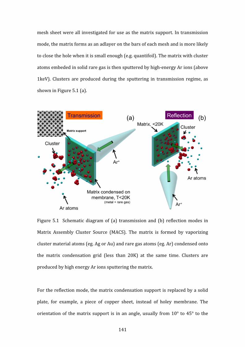
141
mesh sheet were all investigated for use as the matrix support. In transmission
mode, the matrix forms as an adlayer on the bars of each mesh and is more likely
to close the hole when it is small enough (e.g. quantifoil). The matrix with cluster
atoms embeded in solid rare gas is then sputtered by high-‐energy Ar ions (above
1keV). Clusters are produced during the sputtering in transmission regime, as
shown in Figure 5.1 (a).
Figure 5.1 Schematic diagram of (a) transmission and (b) reflection modes in
Matrix Assembly Cluster Source (MACS). The matrix is formed by vaporizing
cluster material atoms (eg. Ag or Au) and rare gas atoms (eg. Ar) condensed onto
the matrix condensation grid (less than 20K) at the same time. Clusters are
produced by high energy Ar ions sputtering the matrix.
For the reflection mode, the matrix condensation support is replaced by a solid
plate, for example, a piece of copper sheet, instead of holey membrane. The
orientation of the matrix support is in an angle, usually from 10° to 45° to the
142
direction of incident ion beam. Clusters are produced following the same
procedure just described but collected in reflection regime as shown in Figure
5.1(b). In this chapter, only transmission mode is used to demonstrate the
principle of the MACS as well as preliminary study of effects of matrix
parameters. Reflection mode will be discussed in chapter 6.
5.1.3 Methodology
The production of clusters in the MACS is based on a high-‐energy (>1keV) atomic
(e.g. Ar+) ion beam bombarding a condensed matrix of rare gas atoms. The
matrix is Ar impregnated with atoms of desired cluster materials, including Ag or
Au. The cluster formation process is possible through two mechanisms:
(i) Clusters are preformed during the condensation of the matrix. The
matrix is formed by simultaneously condensing of atoms cluster materials and
rare gas. In the matrix, cluster material atoms are driven into small clusters by
the potential force to minimize the energy [2-‐5]. This process happens as soon as
the cluster material atoms land in the matrix and only lasts around 20ps.
(ii) Clusters are aggregated through the ion impact. Due to the momentum
delivered into matrix with high-‐energy ion impact, small clusters and cluster
material atoms inside the matrix become mobile and aggregate into bigger
clusters. Clusters keep growing with multiple ion impacts because of
successively delivered momentum and the depletion of rare gas atoms [6-‐8].
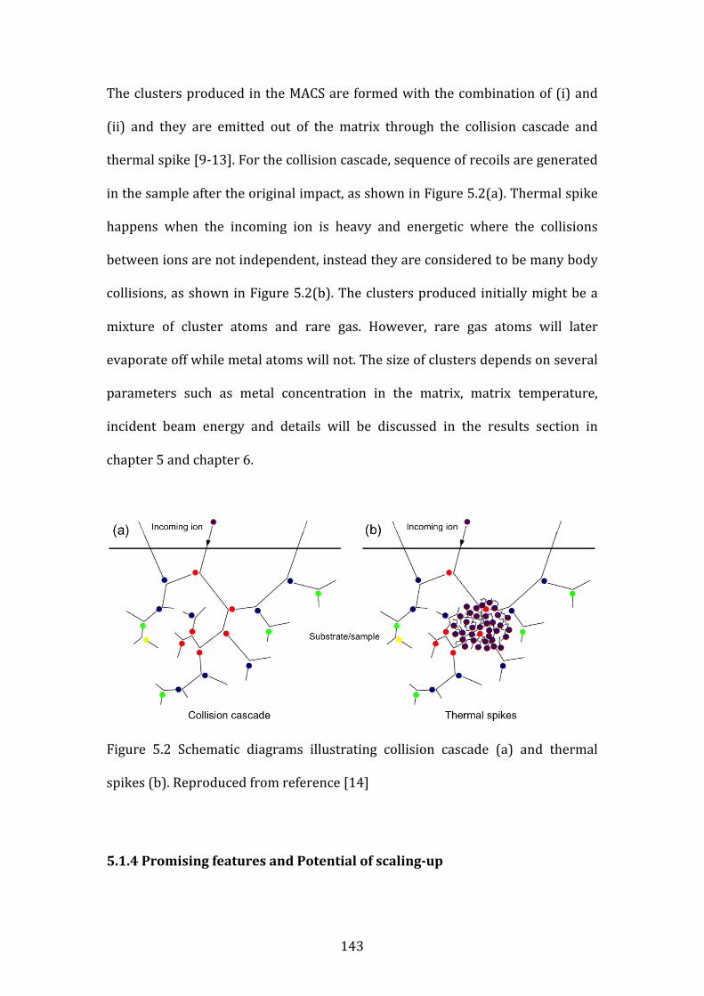
143
The clusters produced in the MACS are formed with the combination of (i) and
(ii) and they are emitted out of the matrix through the collision cascade and
thermal spike [9-‐13]. For the collision cascade, sequence of recoils are generated
in the sample after the original impact, as shown in Figure 5.2(a). Thermal spike
happens when the incoming ion is heavy and energetic where the collisions
between ions are not independent, instead they are considered to be many body
collisions, as shown in Figure 5.2(b). The clusters produced initially might be a
mixture of cluster atoms and rare gas. However, rare gas atoms will later
evaporate off while metal atoms will not. The size of clusters depends on several
parameters such as metal concentration in the matrix, matrix temperature,
incident beam energy and details will be discussed in the results section in
chapter 5 and chapter 6.
Figure 5.2 Schematic diagrams illustrating collision cascade (a) and thermal
spikes (b). Reproduced from reference [14]
5.1.4 Promising features and Potential of scaling-‐up
144
Based on the results obtained so far, the clusters produced using the MACS
techniques exhibit a “narrow” size distribution (M/ΔM>1) without mass
selection. Moreover, the size of clusters can be controlled by the experimental
parameters primarily the metal concentration in the matrix. These two features
enable the production of size-‐selected clusters, e.g. for catalysis purpose, using
the MACS techniques without additional mass selection, which results in a
higher-‐usage ratio of the clusters. The aim of the MACS technology is to scale up
the cluster production rate by ~7 order of magnitude, from 0.1-‐1nA to 1-‐10mA,
which is equivalent to grams of clusters per day. In principle, the cluster
production rate in the MACS is a function of the incident ion beam current, and
ion beam sources with output current up to 10A are available. The ion to cluster
ratio (how many incident ions are required to produce one cluster) based on our
current experimental results is 0.05% for transmission mode and nearly 0.5%
for reflection mode. Therefore, a cluster beam current equivalent to 10mA is
achievable. Of course the precondition is the matrix has a sufficient
replenishment rate.
This chapter concentrates on the proof-‐of-‐principle of the MACS idea and
preliminary studies of effect of experimental parameters on cluster production
using MACS demonstration apparatus. In chapter 6, we report the development
of the upgraded apparatus, MACS 1, to scale up the cluster production rate and
systematically investigate the controlled cluster production to better understand
the methodologies.
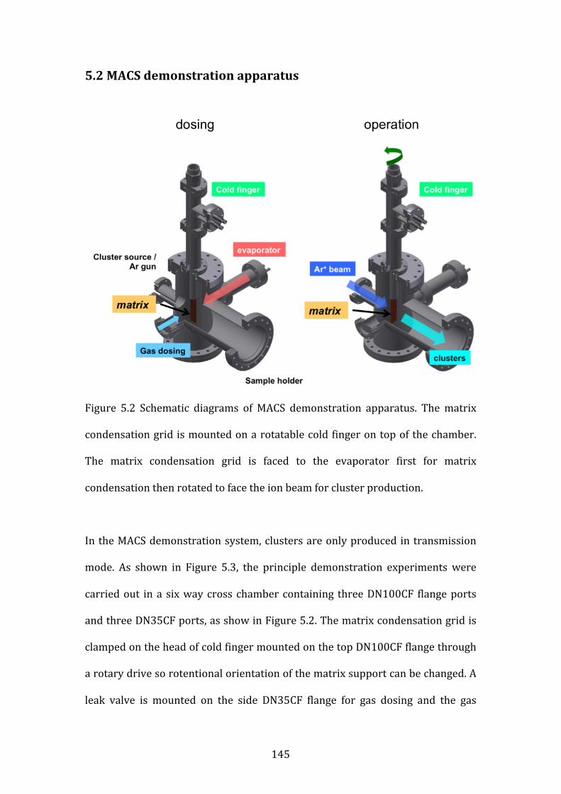
145
5.2 MACS demonstration apparatus
Figure 5.2 Schematic diagrams of MACS demonstration apparatus. The matrix
condensation grid is mounted on a rotatable cold finger on top of the chamber.
The matrix condensation grid is faced to the evaporator first for matrix
condensation then rotated to face the ion beam for cluster production.
In the MACS demonstration system, clusters are only produced in transmission
mode. As shown in Figure 5.3, the principle demonstration experiments were
carried out in a six way cross chamber containing three DN100CF flange ports
and three DN35CF ports, as show in Figure 5.2. The matrix condensation grid is
clamped on the head of cold finger mounted on the top DN100CF flange through
a rotary drive so rotentional orientation of the matrix support can be changed. A
leak valve is mounted on the side DN35CF flange for gas dosing and the gas
146
dosing rate is monitored by the Penning gauge. The evaporator is mounted on
the other side for cluster materials vaporization. The whole chamber is
connected to a magnetron sputtering cluster source as the Ar ion beam used to
sputter the matrix is generated in the cluster source at the early stage. A sample
holder containing 6 TEM grids is mounted on the back DN100CF flange port in
line with Ar beam and matrix to collect produced clusters.
5.2.1 Matrix condensation support
Several different types of grids for matrix condensation were tested in the
demonstration experiments, in order to study the effects on cluster size and flux.
The grid types includes 400, 1000, 2000 mesh copper grid and quantifoil (15-‐
20nm carbon film with array of same size holes). All of them are 3 mm in
diameter. The specifications for each grid are summarized in Table 5.1.
Matrix support grid type Hole width/diameter
Bar width/diameter
Transmission ratio
400 mesh 37μm 25 μm 37% 1000 mesh 19 μm 6 μm 57% 2000 mesh 6.5 μm 6 μm 41%
Quantifoil 1.2/1.3 1.2 μm 1.3 μm 11% Table 5.1 Specification of different type matrix condensation grid.
5.2.2 Cryogenic cooling
The cold finger used in the principle demonstration system is made of a hollow
stainless steel tube with an oxygen-‐free copper block welded on the top to hold
the matrix support. The matrix support is clamped on the copper part and is
electrically isolated from the whole cold finger using a sapphire plate. This
147
arrangement allows for a bias voltage to be applied to the matrix support and
current of the incident ion beam to be measured. The incident beam current on
the matrix support is read by the Keithley 6485 picoammeter. To maintain the
good thermal conductivity, the sapphire was coated with gold on both sides
using Edwards commercial evaporator. The cooling is provided by injecting
liquid helium flow from Dewar bottle directly deliver to the copper part of cold
finger through a transfer line. An oil free scroll pump is used to maintain the flow
by pumping helium gas out. The cooling power can be controlled by adjusting the
regulator in the pumping line.
5.2.3 Temperature measurement
The temperature of the matrix support can be cooled to below 20K in ~1.5 hours
and the lowest temperature recorded was 9K. The temperature of the matrix
condensation support is measured using the Rhodium-‐Iron temperature sensor
mounted on top of the cold finger just beside the matrix condensation support.
The Lakeshore 340 temperature controller is used to monitor the temperature.
The calibration curve for the temperature sensor has been calibrated at 3 points,
ice water, liquid nitrogen and liquid helium, to achieve accuracy measurement.
5.2.4 Evaporation
A thermal evaporator is used to vaporize cluster material in the demonstration
system. The cluster material (e.g. Au and Ag) is filled in a Tantalum boat and the
boat is heated up by high DC current. A quartz crystal microbalance (QCM, from
148
Digi-‐key ATS060, 6MHz) is mounted in front of the evaporator to monitor the
evaporation speed. The evaporation speed is monitored by reading the
frequency of the QCM using the thin film rate/thickness transducer from Sycon
instruments. In order to determine the correct evaporation speed on the matrix,
another QCM is mounted on the cold finger temperately, at the same position as
the matrix support, for calibration before carrying out cluster production. The
QCM on the cold finger is removed when preparing clusters as it will affect the
cooling of the matrix condensation support. Five different evaporation speeds
have been tested for the calibration and the real evaporation speed on the matrix
is approximately 5 times less than the reading from QCM in front of evaporator.
Details are shown in Table 5.2.
QCM in front of
evaporator
QCM at position of matrix
condensation grid
0.3Å/s 0.05Å/s
0.6Å/s 0.11Å/s
1Å/s 0.18Å/s
1.2Å/s 0.25Å/s
2Å/s 0.36Å/s
Table 5.2 Evaporation speed measured by QCM mounted in front evaporator and
on the position same as the matrix condensation grid.
To provide additional verification of the evaporation rate, we also measured the
thickness of metal deposited to a silicon wafer mounted at same position as the
matrix condensation grid comparing to the QCM value. A 400 mesh TEM grid is
attached to the silicon wafer as the mask to create patterns. The height of Ag film
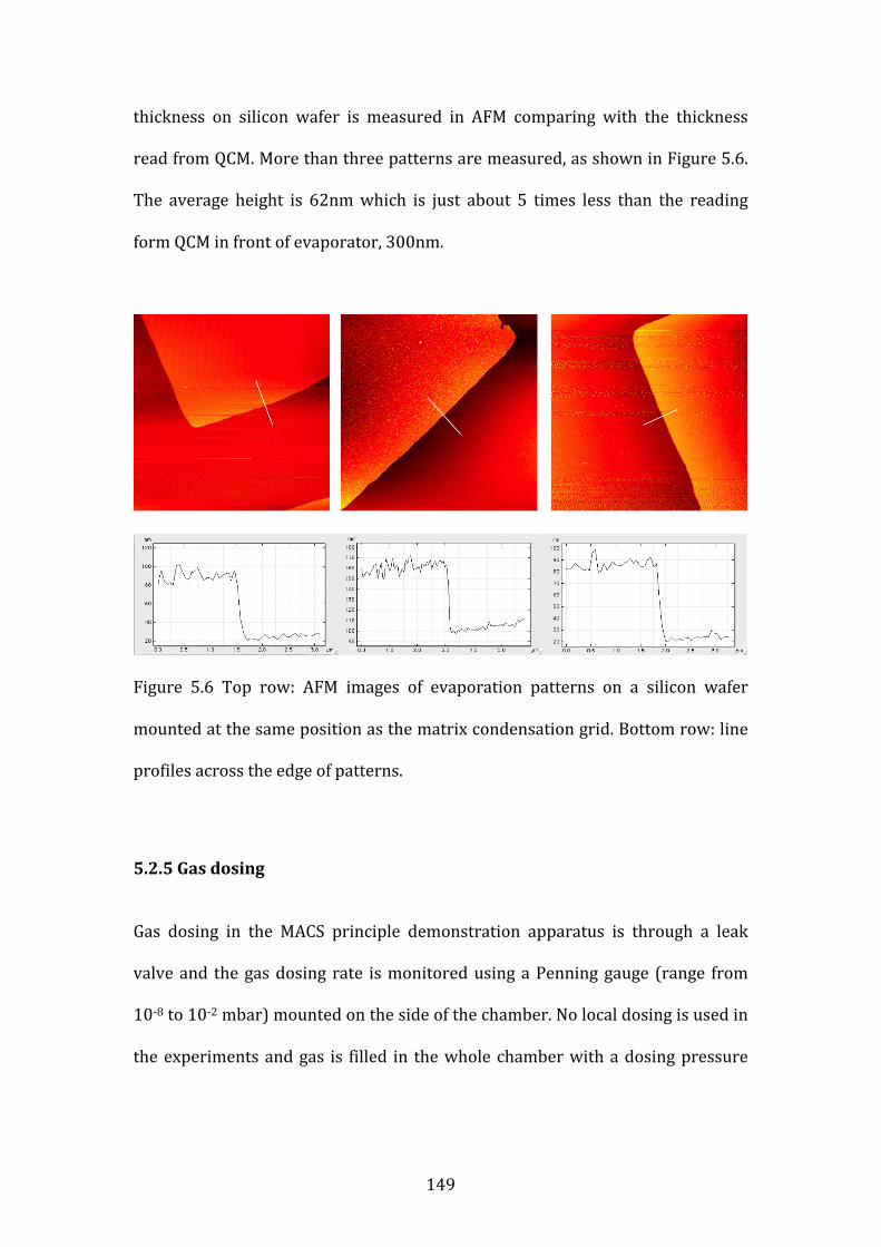
149
thickness on silicon wafer is measured in AFM comparing with the thickness
read from QCM. More than three patterns are measured, as shown in Figure 5.6.
The average height is 62nm which is just about 5 times less than the reading
form QCM in front of evaporator, 300nm.
Figure 5.6 Top row: AFM images of evaporation patterns on a silicon wafer
mounted at the same position as the matrix condensation grid. Bottom row: line
profiles across the edge of patterns.
5.2.5 Gas dosing
Gas dosing in the MACS principle demonstration apparatus is through a leak
valve and the gas dosing rate is monitored using a Penning gauge (range from
10-‐8 to 10-‐2 mbar) mounted on the side of the chamber. No local dosing is used in
the experiments and gas is filled in the whole chamber with a dosing pressure
150
between 10-‐7 and 10-‐6 mbar when preparing clusters. The matrix formation gas
used is Ar here and the base pressure in the chamber is 10-‐8 mbar.
5.2.6 Ar ion beam
Two different Ar+ ion beam sources are used in the principle demonstration
experiments: Ar+ ion beam from magnetron sputtering source and Ar ion gun for
scale-‐up the cluster flux. When using the Ar+ ion beam from magnetron
sputtering cluster source, the cluster generation chamber is connected to the exit
of ToF mass filter of the magnetron sputtering cluster source. The Ar ion beam is
generated in the magnetron sputtering cluster source and filtered out by the ToF
mass filter to avoid any metal ions produced by sputtering. As mentioned
previously, in the magnetron sputtering cluster source the Ar plasma is ignited
by the potential applied on the magnetron head, powered by either DC power
supply or RF power supply. The Ar plasma formed in the generation chamber is
then extracted and focused into a beam by electrical fields applied on a set of ion
optics. Finally the Ar ion beam is filtered out by the ToF mass filter and delivered
to the MACS chamber through another set of ion optic lenses [15-‐16]. The energy
of Ar beam generated from magnetron sputtering cluster source is defined by the
potential applied on the terminal plate, which is the matrix here. In most cases
the bias voltage on the cold finger is -‐950V meaning the energy of Ar ion beam
hitting the matrix is 950eV. The maximum voltage we are able to apply on the
cold finger is ±3000V. The spot size of Ar ion beam is around 5mm in diameter
and maximum current detected on cold finger can be up to 10nA at 950V bias
voltage.
151
The Ar ion gun used is a cold cathode ion source ISE 5 from Omicron, which is
able to generate a maximum ion beam current of 80μA with beam energy from
250eV to 5keV. The Ar ion beam generated in this ion source is via the
mechanism of gas discharge between cathode and anode in a gas cell when a
high voltage is applied. The gas discharge region is surrounded by a longitudinal
magnetic field forcing electrons to spiral which extends the path to generate a
large quantity of ions and electrons. The ions generated inside gas cell are then
extracted through an aperture on the kinetic plate into flight tube. The energy of
the Ar beam generated in Ar ion gun can be controlled by tuning the voltage
difference between the kinetic plate and flight tube. Also an electrical ion optic
lens is mounted in the front of the flight tube of the ion source to control the spot
size of out coming ion beam. The incident Ar ion beam current on the cold finger
is measured by the picoammeter, Keithley 6485. The picoammeter is floated and
a circuit (based on Keithley manual) is built connecting to the picoammeter
enabling to apply bias voltage on the cold finger while measuring the current.
The picoammeter is biased at the same potential as the cold finger, and in order
to isolate the picoammeter from the operator and other equipment it is enclosed
in insulating box.
5.3 Sample preparation
Samples were produced to demonstrate the principle of the matrix assembly
cluster source, as well as study effects of different parameters on cluster size and
flux. The sample preparation procedures can be divided into the following steps.
152
(a) Preparation work
The chamber is pumped down to below 5x10-‐8 mbar before starting the
experiments, which is almost the best vacuum that can be achieved at room
temperature without baking the system. The evaporator is degassed by heating
up to above 600°C for 30mins. Ar ion beam is optimized to reach the certain
beam current on cold finger. For Ar ion beam from cluster source, the beam
current is optimized by tuning the gas flow, voltages on nozzle, skimmers and ion
optic lenses. For the Ar ion gun, the beam current can be tuned just on the front
panel on the controller to set beam energy, emission current as well as focus.
After preparation of the incident Ar ion beam, the cold finger is cooled down by
liquid helium to below 20K. The pressure of the chamber reaches to 10-‐9 mbar
after cooling as the cooled cold finger is working as a cryogenic pump.
(b) Condensation of the matrix
The matrix condensation support is rotated to face the evaporator for matrix
condensation. The evaporator is heated up to achieve a stable evaporation flux
measured by the QCM in front of the evaporator, before opening the shutter. The
evaporation and gas dosing start simultaneously. Gas dosing rate on the matrix is
controlled by the gas pressure monitored by the penning gauge. The matrix
growth time is recorded by a stop watch.
(c) Deposition of clusters
After the matrix condensation, the cold finger is rotated back in line with ion
beam and sample holder. Similar to that in magnetron source, the sample holder
is biased by high voltage power supply and connected to ground through the
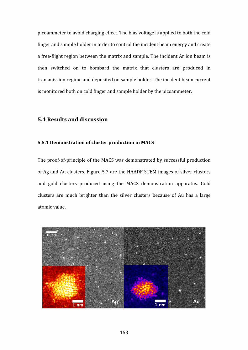
153
picoammeter to avoid charging effect. The bias voltage is applied to both the cold
finger and sample holder in order to control the incident beam energy and create
a free-‐flight region between the matrix and sample. The incident Ar ion beam is
then switched on to bombard the matrix that clusters are produced in
transmission regime and deposited on sample holder. The incident beam current
is monitored both on cold finger and sample holder by the picoammeter.
5.4 Results and discussion
5.5.1 Demonstration of cluster production in MACS
The proof-‐of-‐principle of the MACS was demonstrated by successful production
of Ag and Au clusters. Figure 5.7 are the HAADF STEM images of silver clusters
and gold clusters produced using the MACS demonstration apparatus. Gold
clusters are much brighter than the silver clusters because of Au has a large
atomic value.
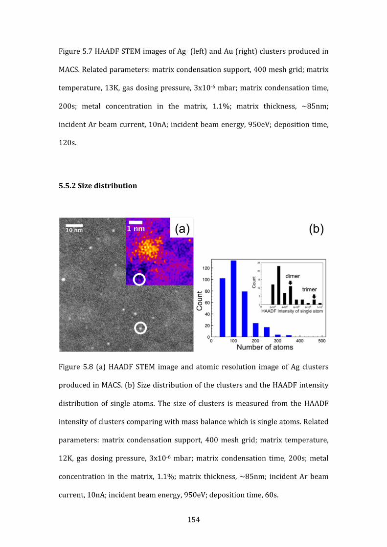
154
Figure 5.7 HAADF STEM images of Ag (left) and Au (right) clusters produced in
MACS. Related parameters: matrix condensation support, 400 mesh grid; matrix
temperature, 13K, gas dosing pressure, 3x10-‐6 mbar; matrix condensation time,
200s; metal concentration in the matrix, 1.1%; matrix thickness, ~85nm;
incident Ar beam current, 10nA; incident beam energy, 950eV; deposition time,
120s.
5.5.2 Size distribution
Figure 5.8 (a) HAADF STEM image and atomic resolution image of Ag clusters
produced in MACS. (b) Size distribution of the clusters and the HAADF intensity
distribution of single atoms. The size of clusters is measured from the HAADF
intensity of clusters comparing with mass balance which is single atoms. Related
parameters: matrix condensation support, 400 mesh grid; matrix temperature,
12K, gas dosing pressure, 3x10-‐6 mbar; matrix condensation time, 200s; metal
concentration in the matrix, 1.1%; matrix thickness, ~85nm; incident Ar beam
current, 10nA; incident beam energy, 950eV; deposition time, 60s.
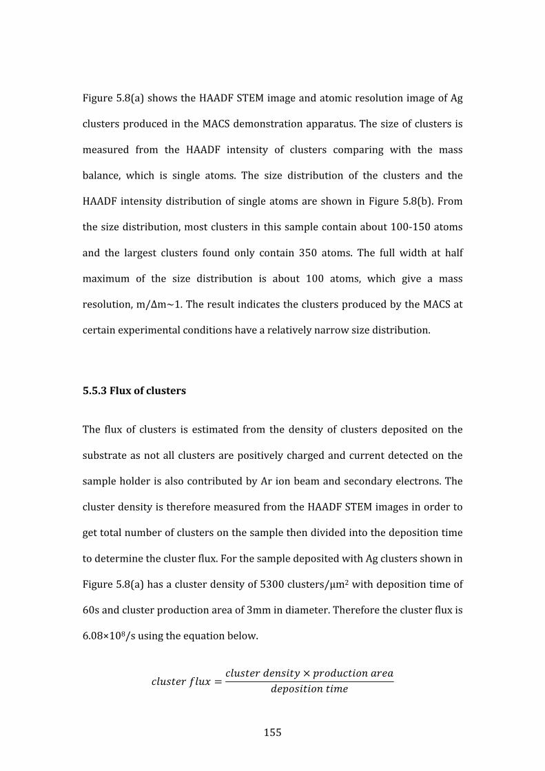
155
Figure 5.8(a) shows the HAADF STEM image and atomic resolution image of Ag
clusters produced in the MACS demonstration apparatus. The size of clusters is
measured from the HAADF intensity of clusters comparing with the mass
balance, which is single atoms. The size distribution of the clusters and the
HAADF intensity distribution of single atoms are shown in Figure 5.8(b). From
the size distribution, most clusters in this sample contain about 100-‐150 atoms
and the largest clusters found only contain 350 atoms. The full width at half
maximum of the size distribution is about 100 atoms, which give a mass
resolution, m/Δm~1. The result indicates the clusters produced by the MACS at
certain experimental conditions have a relatively narrow size distribution.
5.5.3 Flux of clusters
The flux of clusters is estimated from the density of clusters deposited on the
substrate as not all clusters are positively charged and current detected on the
sample holder is also contributed by Ar ion beam and secondary electrons. The
cluster density is therefore measured from the HAADF STEM images in order to
get total number of clusters on the sample then divided into the deposition time
to determine the cluster flux. For the sample deposited with Ag clusters shown in
Figure 5.8(a) has a cluster density of 5300 clusters/μm2 with deposition time of
60s and cluster production area of 3mm in diameter. Therefore the cluster flux is
6.08×10⁸/s using the equation below.
𝑐𝑙𝑢𝑠𝑡𝑒𝑟 𝑓𝑙𝑢𝑥 =𝑐𝑙𝑢𝑠𝑡𝑒𝑟 𝑑𝑒𝑛𝑠𝑖𝑡𝑦 × 𝑝𝑟𝑜𝑑𝑢𝑐𝑡𝑖𝑜𝑛 𝑎𝑟𝑒𝑎
𝑑𝑒𝑝𝑜𝑠𝑖𝑡𝑖𝑜𝑛 𝑡𝑖𝑚𝑒
156
5.5.4 Size control
In addition to the clusters produced in MACS has relatively narrow size
distribution, m/Δm~1, the cluster size can be controlled by tuning the
parameters especially the metal concentration in the matrix. In this work, the
metal concentration in the matrix is determined only by the evaporation speed
as the gas dosing rate is fixed. HAADF STEM images and atomic resolution
images of eight samples prepared with metal concentration from 0.38% to
5.66% are shown in Figure 5.9 (a-‐h) as well as the histograms of size distribution
measured from the integrated HAADF intensity in (i-‐p). A plot of cluster size and
calculated cluster flux as a function of metal concentration in the matrix is shown
in Figure 5.10.
As shown in the plot, it is clear that the size of clusters produced by the MACS is
increased significantly, with a power of 2, with the metal concentration in the
matrix. However, the flux of clusters decreases rapidly with a power of 2.5. The
size distributions of clusters produced remain relatively narrow, m/Δm~1,
across the parameter space.
As mentioned in the methodology section, cluster formation process is probably
through two mechanisms. For both routines, with higher metal concentration in
the matrix, clusters more easily capture other atoms to grow larger due to the
higher density of cluster material atoms. The decrease in the cluster flux is due to
the fact that a matrix with a heavier metal loading matrix is harder to sputter and
larger clusters are relatively harder to be knocked out the matrix [19-‐23].
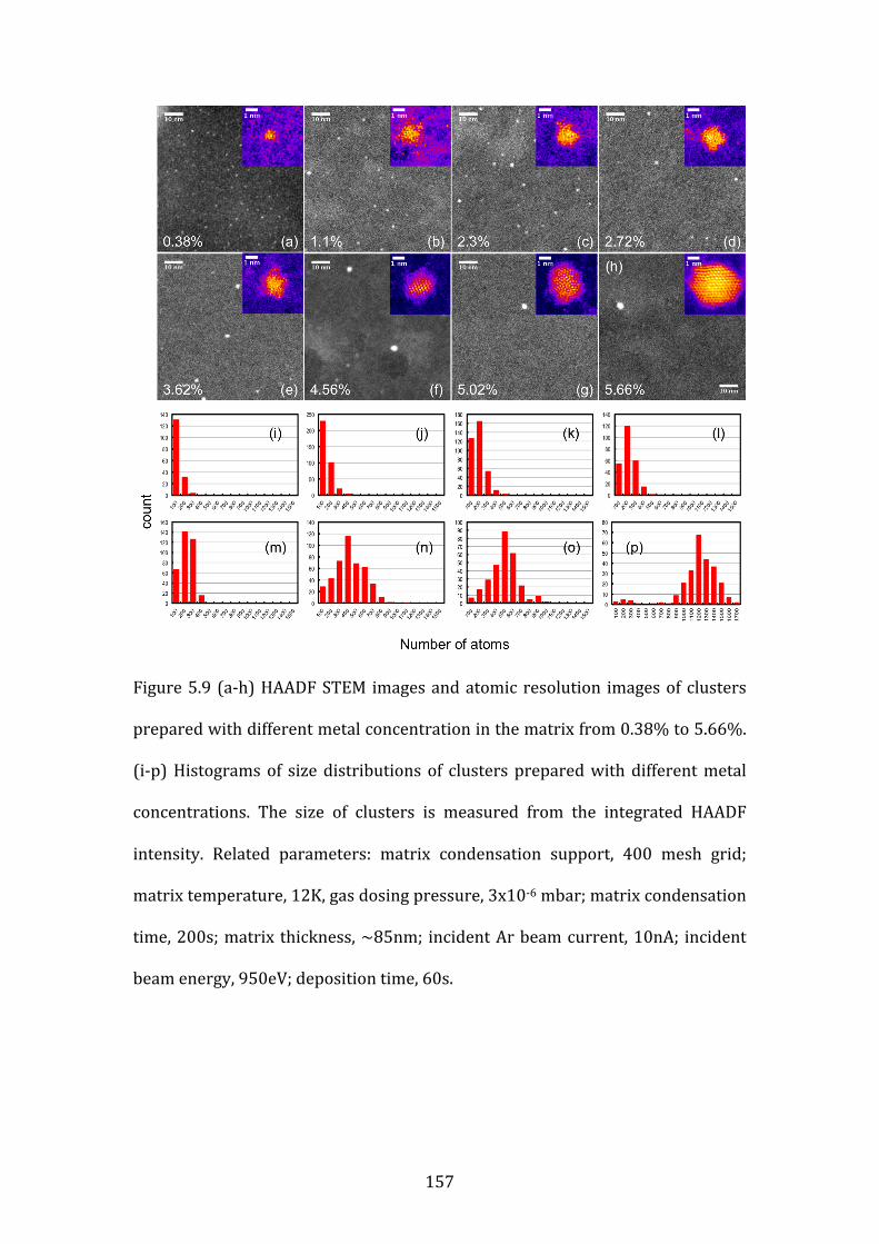
157
Figure 5.9 (a-‐h) HAADF STEM images and atomic resolution images of clusters
prepared with different metal concentration in the matrix from 0.38% to 5.66%.
(i-‐p) Histograms of size distributions of clusters prepared with different metal
concentrations. The size of clusters is measured from the integrated HAADF
intensity. Related parameters: matrix condensation support, 400 mesh grid;
matrix temperature, 12K, gas dosing pressure, 3x10-‐6 mbar; matrix condensation
time, 200s; matrix thickness, ~85nm; incident Ar beam current, 10nA; incident
beam energy, 950eV; deposition time, 60s.
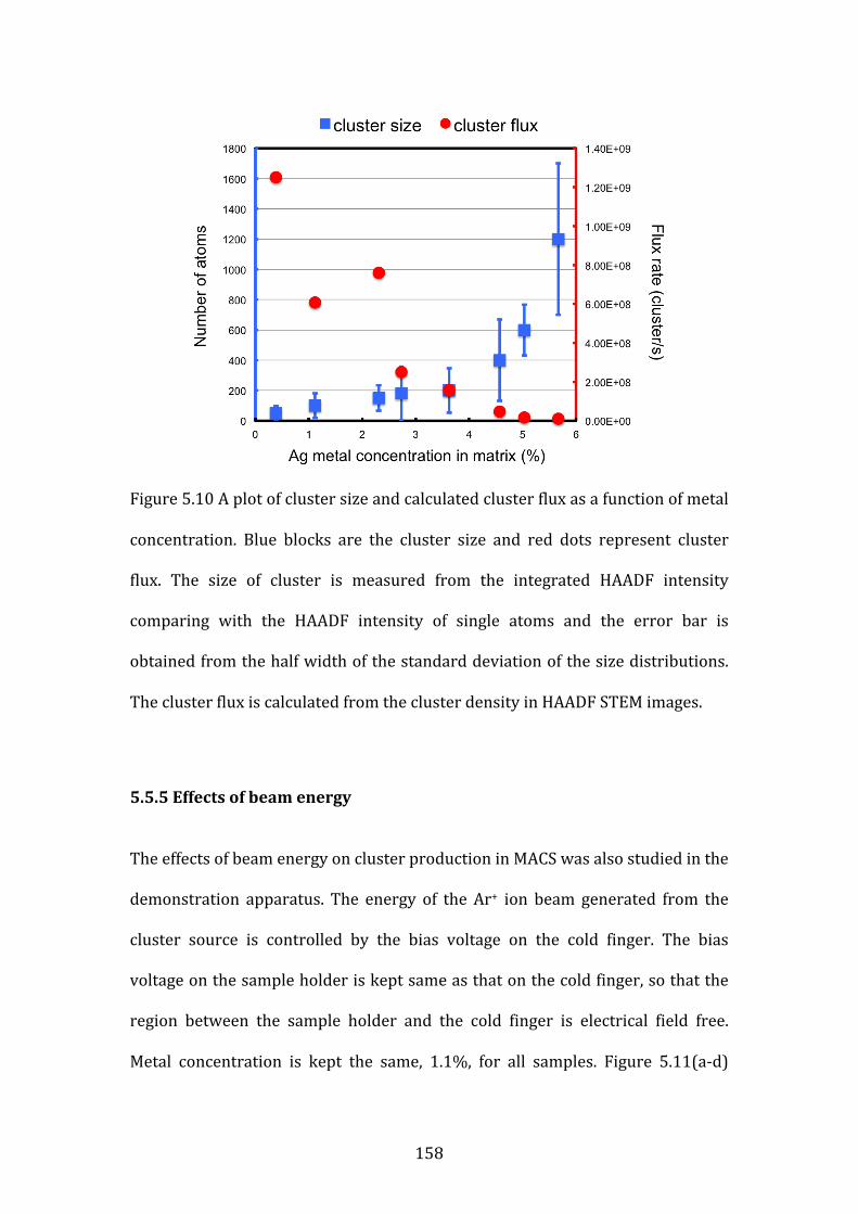
158
Figure 5.10 A plot of cluster size and calculated cluster flux as a function of metal
concentration. Blue blocks are the cluster size and red dots represent cluster
flux. The size of cluster is measured from the integrated HAADF intensity
comparing with the HAADF intensity of single atoms and the error bar is
obtained from the half width of the standard deviation of the size distributions.
The cluster flux is calculated from the cluster density in HAADF STEM images.
5.5.5 Effects of beam energy
The effects of beam energy on cluster production in MACS was also studied in the
demonstration apparatus. The energy of the Ar+ ion beam generated from the
cluster source is controlled by the bias voltage on the cold finger. The bias
voltage on the sample holder is kept same as that on the cold finger, so that the
region between the sample holder and the cold finger is electrical field free.
Metal concentration is kept the same, 1.1%, for all samples. Figure 5.11(a-‐d)
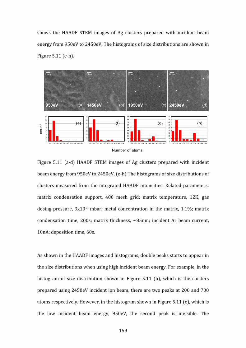
159
shows the HAADF STEM images of Ag clusters prepared with incident beam
energy from 950eV to 2450eV. The histograms of size distributions are shown in
Figure 5.11 (e-‐h).
Figure 5.11 (a-‐d) HAADF STEM images of Ag clusters prepared with incident
beam energy from 950eV to 2450eV. (e-‐h) The histograms of size distributions of
clusters measured from the integrated HAADF intensities. Related parameters:
matrix condensation support, 400 mesh grid; matrix temperature, 12K, gas
dosing pressure, 3x10-‐6 mbar; metal concentration in the matrix, 1.1%; matrix
condensation time, 200s; matrix thickness, ~85nm; incident Ar beam current,
10nA; deposition time, 60s.
As shown in the HAADF images and histograms, double peaks starts to appear in
the size distributions when using high incident beam energy. For example, in the
histogram of size distribution shown in Figure 5.11 (h), which is the clusters
prepared using 2450eV incident ion beam, there are two peaks at 200 and 700
atoms respectively. However, in the histogram shown in Figure 5.11 (e), which is
the low incident beam energy, 950eV, the second peak is invisible. The
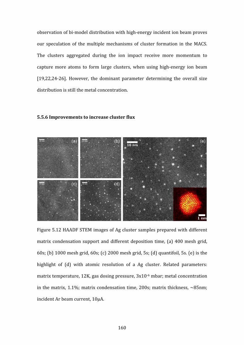
160
observation of bi-‐model distribution with high-‐energy incident ion beam proves
our speculation of the multiple mechanisms of cluster formation in the MACS.
The clusters aggregated during the ion impact receive more momentum to
capture more atoms to form large clusters, when using high-‐energy ion beam
[19,22,24-‐26]. However, the dominant parameter determining the overall size
distribution is still the metal concentration.
5.5.6 Improvements to increase cluster flux
Figure 5.12 HAADF STEM images of Ag cluster samples prepared with different
matrix condensation support and different deposition time, (a) 400 mesh grid,
60s; (b) 1000 mesh grid, 60s; (c) 2000 mesh grid, 5s; (d) quantifoil, 5s. (e) is the
highlight of (d) with atomic resolution of a Ag cluster. Related parameters:
matrix temperature, 12K, gas dosing pressure, 3x10-‐6 mbar; metal concentration
in the matrix, 1.1%; matrix condensation time, 200s; matrix thickness, ~85nm;
incident Ar beam current, 10μA.
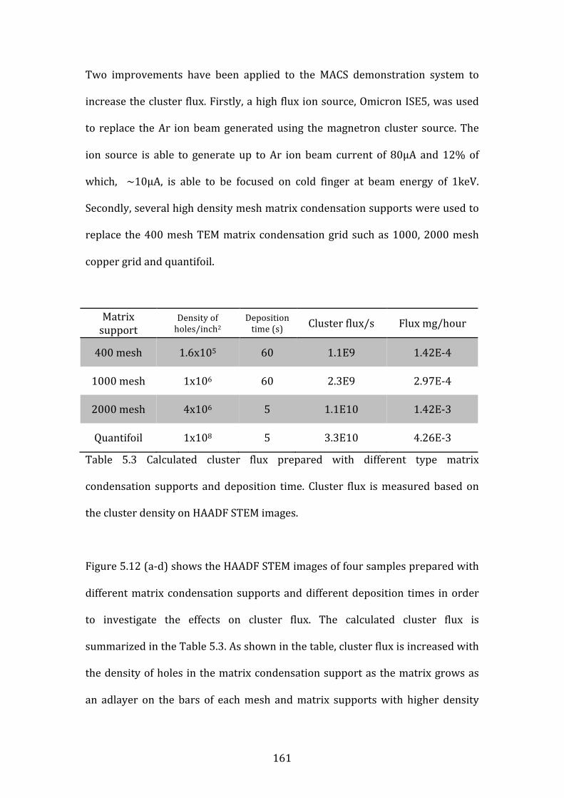
161
Two improvements have been applied to the MACS demonstration system to
increase the cluster flux. Firstly, a high flux ion source, Omicron ISE5, was used
to replace the Ar ion beam generated using the magnetron cluster source. The
ion source is able to generate up to Ar ion beam current of 80μA and 12% of
which, ~10μA, is able to be focused on cold finger at beam energy of 1keV.
Secondly, several high density mesh matrix condensation supports were used to
replace the 400 mesh TEM matrix condensation grid such as 1000, 2000 mesh
copper grid and quantifoil.
Matrix support
Density of holes/inch2
Deposition time (s) Cluster flux/s Flux mg/hour
400 mesh 1.6x10⁵ 60 1.1E9 1.42E-‐4
1000 mesh 1x10⁶ 60 2.3E9 2.97E-‐4
2000 mesh 4x10⁶ 5 1.1E10 1.42E-‐3
Quantifoil 1x10⁸ 5 3.3E10 4.26E-‐3
Table 5.3 Calculated cluster flux prepared with different type matrix
condensation supports and deposition time. Cluster flux is measured based on
the cluster density on HAADF STEM images.
Figure 5.12 (a-‐d) shows the HAADF STEM images of four samples prepared with
different matrix condensation supports and different deposition times in order
to investigate the effects on cluster flux. The calculated cluster flux is
summarized in the Table 5.3. As shown in the table, cluster flux is increased with
the density of holes in the matrix condensation support as the matrix grows as
an adlayer on the bars of each mesh and matrix supports with higher density
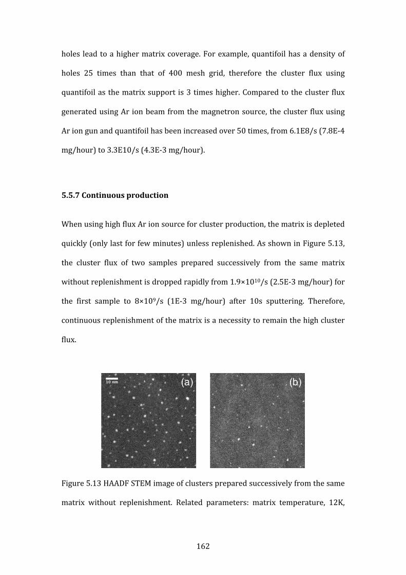
162
holes lead to a higher matrix coverage. For example, quantifoil has a density of
holes 25 times than that of 400 mesh grid, therefore the cluster flux using
quantifoil as the matrix support is 3 times higher. Compared to the cluster flux
generated using Ar ion beam from the magnetron source, the cluster flux using
Ar ion gun and quantifoil has been increased over 50 times, from 6.1E8/s (7.8E-‐4
mg/hour) to 3.3E10/s (4.3E-‐3 mg/hour).
5.5.7 Continuous production
When using high flux Ar ion source for cluster production, the matrix is depleted
quickly (only last for few minutes) unless replenished. As shown in Figure 5.13,
the cluster flux of two samples prepared successively from the same matrix
without replenishment is dropped rapidly from 1.9×10¹⁰/s (2.5E-‐3 mg/hour) for
the first sample to 8×10⁹/s (1E-‐3 mg/hour) after 10s sputtering. Therefore,
continuous replenishment of the matrix is a necessity to remain the high cluster
flux.
Figure 5.13 HAADF STEM image of clusters prepared successively from the same
matrix without replenishment. Related parameters: matrix temperature, 12K,
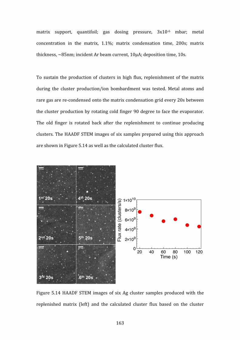
163
matrix support, quantifoil; gas dosing pressure, 3x10-‐6 mbar; metal
concentration in the matrix, 1.1%; matrix condensation time, 200s; matrix
thickness, ~85nm; incident Ar beam current, 10μA; deposition time, 10s.
To sustain the production of clusters in high flux, replenishment of the matrix
during the cluster production/ion bombardment was tested. Metal atoms and
rare gas are re-‐condensed onto the matrix condensation grid every 20s between
the cluster production by rotating cold finger 90 degree to face the evaporator.
The old finger is rotated back after the replenishment to continue producing
clusters. The HAADF STEM images of six samples prepared using this approach
are shown in Figure 5.14 as well as the calculated cluster flux.
Figure 5.14 HAADF STEM images of six Ag cluster samples produced with the
replenished matrix (left) and the calculated cluster flux based on the cluster
164
density in HAADF STEM images (right). Related parameters: matrix temperature,
12K, matrix support, quantifoil; gas dosing pressure, 3x10-‐6 mbar; metal
concentration in the matrix, 1.1%; matrix replenishing time, 100s; matrix
thickness, ~85nm; incident Ar beam current, 10μA; deposition time, 20s.
With the replenishment, cluster flux only decreases slightly (less than 50% after
2 minutes) with time and the downward trend seems reach a stable flux of
clusters around 4×10⁹/s (5.2E-‐4 mg/hour) after 120s, which indicates high flux
of clusters can be continuously produced by simply replenishing the matrix. In
our MACS demonstration apparatus, the cluster production has to be interrupted
during the matrix replenishment. However, with a new chamber design in the
future, the evaporator will be mounted in line with the Ar+ ion gun, matrix
support and sample holder. The condensation of matrix and the deposition will
be taking place at the same time. The continuous high flux of clusters will be
achieved with careful selected condensation rate and the deposition rate.
5.6 Summary
In this chapter, the idea of cluster production using MACS technology has been
introduced. The MACS demonstration experimental apparatus was designed and
built. The methodology of cluster formation in the matrix was explained. The
proof-‐of-‐principle of cluster production in the MACS was demonstrated by the
successful production of Au and Ag clusters. The effects of parameters such as
metal concentration and incident beam energy on cluster production were
preliminarily studied. Results show the clusters produced using the MACS
165
method had relatively narrow size distributions (M/ΔM~1) and cluster size was
sensitive to the metal concentration in the matrix, with a higher metal
concentration making larger clusters. However, the flux of cluster decreases with
the metal loading percentage in the matrix. Incident beam energy also affected
the cluster size. Two improvements, high flux ion source and high-‐density matrix
supports, were applied to scale up the cluster production rate. At last continuous
production was tested by the replenishment of the matrix.
In the next chapter, we will introduce an upgraded MACS apparatus, the MACS 1,
in order to scale up the cluster production rate. Also systematically investigation
cluster formation mechanisms, charge fraction and the mass spectra
measurement of clusters are discussed.
166
List of references
[1] Habibpour, Vahideh, et al. "Catalytic oxidation of cyclohexane by size-‐selected
palladium clusters pinned on graphite." Journal of Experimental Nanoscience 8.7-‐
8 (2013): 993-‐1003.
[2] Silvera, Isaac F., and Victor V. Goldman. "The isotropic intermolecular
potential for H2 and D2 in the solid and gas phases." The Journal of Chemical
Physics 69.9 (1978): 4209-‐4213.
[3] Mirsky, Kira. "Carbon monoxide molecules in an argon matrix: empirical
evaluation of the Ar· Ar, C· Ar and O· Ar potential parameters." Chemical Physics
46.3 (1980): 445-‐455.
[4] Tang, K. T., and J. Peter Toennies. "New combining rules for well parameters
and shapes of the van der Waals potential of mixed rare gas systems." Zeitschrift
für Physik D Atoms, Molecules and Clusters 1.1 (1986): 91-‐101.
[5] Mann, D. E., N. Acquista, and David White. "Infrared Spectra of HCl, DCl, HBr,
and DBr in Solid Rare‐Gas Matrices." The Journal of Chemical Physics 44.9
(1966): 3453-‐3467.
[6] Makeev, Maxim A., and Albert-‐László Barabási. "Ion-‐induced effective surface
diffusion in ion sputtering." Applied physics letters 71.19 (1997): 2800-‐2802.
[7] Winters, Harold F., et al. "Energy transfer from rare gases to surfaces:
Collisions with gold and platinum in the range 1–4000 eV." Physical Review
B41.10 (1990): 6240.
[8] Coufal, H., et al. "Energy transfer from noble-‐gas ions to surfaces: Collisions
with carbon, silicon, copper, silver, and gold in the range 100–4000 eV."Physical
Review B 44.10 (1991): 4747.
167
[9] Averback, R. S., and T. Diaz de la Rubia. "Displacement damage in irradiated
metals and semiconductors." Solid State Physics 51 (1997): 281-‐402.
[10] Smith, Roger. Atomic and ion collisions in solids and at surfaces: theory,
simulation and applications. Cambridge University Press, 2005.
[11] De La Rubia, T. Diaz, et al. "Role of thermal spikes in energetic displacement
cascades." Physical review letters 59.17 (1987): 1930.
[12] Aderjan, Ralf, and Herbert M. Urbassek. "Molecular-‐dynamics study of
craters formed by energetic Cu cluster impact on Cu." Nuclear Instruments and
Methods in Physics Research Section B: Beam Interactions with Materials and
Atoms 164 (2000): 697-‐704.
[13] Nordlund, K., et al. "Defect production in collision cascades in elemental
semiconductors and fcc metals." Physical Review B 57.13 (1998): 7556.
[14] https://en.wikipedia.org/wiki/Collision_cascade
[15] Pratontep, S., et al. "Size-‐selected cluster beam source based on radio
frequency magnetron plasma sputtering and gas condensation." Review of
scientific instruments 76.4 (2005): 045103.
[16] Von Issendorff, B., and R. E. Palmer. "A new high transmission infinite range
mass selector for cluster and nanoparticle beams." Review of Scientific
Instruments 70.12 (1999): 4497-‐4501.
[17] Young, N. P., et al. "Weighing supported nanoparticles: size-‐selected clusters
as mass standards in nanometrology." Physical review letters 101.24 (2008):
246103.
[18] Abràmoff, Michael D., Paulo J. Magalhães, and Sunanda J. Ram. "Image
processing with ImageJ." Biophotonics international 11.7 (2004): 36-‐42.
168
[19] Balaji, V., et al. "Sputtering yields of condensed rare gases." Nuclear
Instruments and Methods in Physics Research Section B: Beam Interactions with
Materials and Atoms 46.1 (1990): 435-‐440.
[20] Sigmund, Peter. "Theory of sputtering. I. Sputtering yield of amorphous and
polycrystalline targets." Physical review 184.2 (1969): 383.
[21] Behrisch, Rainer, and Klaus Wittmaack, eds. Sputtering by particle
bombardment. Vol. 3. Berlin: Springer, 1983.
[22] Laegreid, Nils, and G. K. Wehner. "Sputtering yields of metals for Ar+ and
Ne+ ions with energies from 50 to 600 eV." Journal of Applied Physics 32.3
(1961): 365-‐369.
[23] Smith, Roger. Atomic and ion collisions in solids and at surfaces: theory,
simulation and applications. Cambridge University Press, 2005.
[24] Steinbrüchel, Christoph. "Universal energy dependence of physical and ion-‐
enhanced chemical etch yields at low ion energy." Applied physics letters 55.19
(1989): 1960-‐1962.
[25] Sigmund, Peter. Elements of sputtering theory. press, 2009.
[26] Zalm, P. C. "Energy dependence of the sputtering yield of silicon bombarded
with neon, argon, krypton, and xenon ions." Journal of Applied Physics 54.5
(1983): 2660-‐2666.
169
Chapter 6 Development of the Matrix
Assembly Cluster Source (MACS)
In the previous chapter, the first experimental apparatus of the Matrix Assembly
Cluster Source (MACS) was introduced and the principle of the MACS was
demonstrated by the production of Au and Ag clusters as well as preliminary
studies of effects of matrix parameters on cluster production. This Chapter
introduces an upgraded experimental setup of the MACS system, the MACS 1, for
scaling up the cluster production rate, not only transmission mode, but also
using the reflection mode. It also includes systematic investigation of the effects
of metal concentration, matrix temperature and incident beam energy on cluster
size and flux. Also, measurements of charge fractions and mass spectra are
reported.
The work presented in this chapter involve a few collaborators. The instrument
design and development were done together by the author and William Terry.
The software and computer interface development for the MACS apparatus were
done by William Terry. The SIMION simulation was done by the author and
170
William Terry. The sample preparations were done by the author, William Terry
(Ag clusters) and Dr. Richard Balog (Au clusters). Charge fractions and mass
spectra measurements were done by the author and Rongsheng Cai.
6.1 Experimental apparatus of MACS 1
6.1.1 Overview
The MACS 1 is the upgraded apparatus based on the principle demonstrated in
the MACS demonstration system discussed in last chapter. The MACS is designed
to scale up the cluster production rate and understand cluster formation
mechanisms by systematic investigation of the experimental parameters.
Compared to the demonstration apparatus, the improvements having been
applied in MACS 1 are highlighted below.
(i) Cooling system; A closed-‐cycle cryocooler was installed to provide the
cooling power for the condensation of the matrix.
(ii) Evaporator; A high temperature effusion cell (up to 2000°C with a crucible
size of 10cc) was employed for the evaporation of cluster materials.
(iii) Ion source and ion optics; High flux ion source with maximum output
current of 4mA was installed. Ion optics was designed and built to focus more
ions onto matrix.
(iv) Matrix condensation support; 1 inch by 1 inch matrix condensation
support was used.
171
(v) Cluster production approaches; Both transmission mode and reflection
mode were used in the MACS 1 for cluster productions.
(vi) Analysis methods; Lateral time-‐of-‐flight mass spectrometer was involved
in in-‐flight analysis of clusters produced in the MACS 1 in addition to the STEM
measurement of deposited clusters.
The schematic diagram of the MACS 1 is shown in Figure 6.1. The apparatus can
be switched from transmission mode (6.1a) to reflection mode (6.1b) by rotating
the matrix support. Figure 6.1(c) shows the MACS 1 apparatus in Nanoscale
Physics Research Laboratory in University of Birmingham.
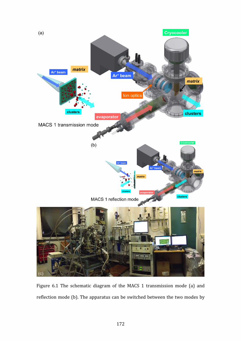
172
Figure 6.1 The schematic diagram of the MACS 1 transmission mode (a) and
reflection mode (b). The apparatus can be switched between the two modes by
173
rotating the matrix support. (c) The MACS 1 apparatus in Nanoscale Physics
Research Laboratory in University of Birmingham.
6.1.2 Cryocooler
The cooling system used in the MACS 1 is a closed cycle cooling system, which is
able to cool down the matrix to around 10K in around 2 hours with a power of
6.7W. The cooling system consists of a cooling head and a compressor both of
which are from Sumitomo cryogenics, the CH-‐204 series. The cooling head is
mounted on top of the generation chamber and it is connected with the
compressor via two transfer lines (supply and return). The working principle of
the cryocooler is similar to a refrigerator in which the cooling head is cooled by
the cold helium gas delivered from the compressor and the hot gas is pumped
back for recycle after cooling.
6.1.3 Matrix condensation support
A 1-‐inch by 1-‐inch matrix condensation support is used in the MACS 1 instead of
3mm grid in the MACS demonstration apparatus to scale up the cluster
production rate. The matrix support used for transmission mode is 1000 copper
mesh with 10μm opening, 15μm line width and 13μm thickness. For
transmission mode, it is a solid copper plate with a thickness of 100μm. The
matrix support is fixed on a sample stage on top of the cryocooler. The stage to
fix the matrix support is a window frame and thin gold foil is filled in the gap
between the stage and the matrix support to maintain good thermal transfer as
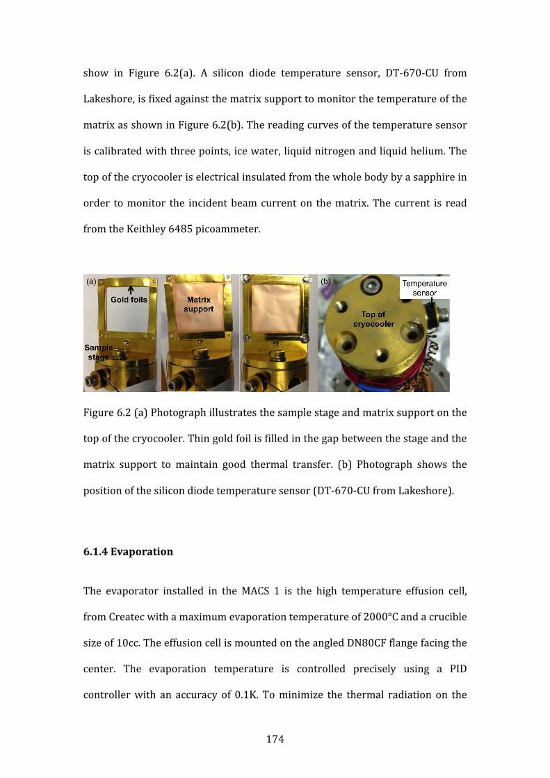
174
show in Figure 6.2(a). A silicon diode temperature sensor, DT-‐670-‐CU from
Lakeshore, is fixed against the matrix support to monitor the temperature of the
matrix as shown in Figure 6.2(b). The reading curves of the temperature sensor
is calibrated with three points, ice water, liquid nitrogen and liquid helium. The
top of the cryocooler is electrical insulated from the whole body by a sapphire in
order to monitor the incident beam current on the matrix. The current is read
from the Keithley 6485 picoammeter.
Figure 6.2 (a) Photograph illustrates the sample stage and matrix support on the
top of the cryocooler. Thin gold foil is filled in the gap between the stage and the
matrix support to maintain good thermal transfer. (b) Photograph shows the
position of the silicon diode temperature sensor (DT-‐670-‐CU from Lakeshore).
6.1.4 Evaporation
The evaporator installed in the MACS 1 is the high temperature effusion cell,
from Createc with a maximum evaporation temperature of 2000°C and a crucible
size of 10cc. The effusion cell is mounted on the angled DN80CF flange facing the
center. The evaporation temperature is controlled precisely using a PID
controller with an accuracy of 0.1K. To minimize the thermal radiation on the
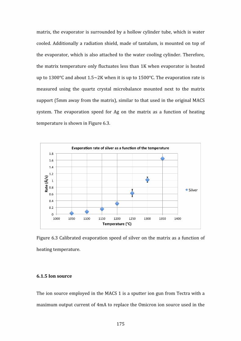
175
matrix, the evaporator is surrounded by a hollow cylinder tube, which is water
cooled. Additionally a radiation shield, made of tantalum, is mounted on top of
the evaporator, which is also attached to the water cooling cylinder. Therefore,
the matrix temperature only fluctuates less than 1K when evaporator is heated
up to 1300°C and about 1.5~2K when it is up to 1500°C. The evaporation rate is
measured using the quartz crystal microbalance mounted next to the matrix
support (5mm away from the matrix), similar to that used in the original MACS
system. The evaporation speed for Ag on the matrix as a function of heating
temperature is shown in Figure 6.3.
Figure 6.3 Calibrated evaporation speed of silver on the matrix as a function of
heating temperature.
6.1.5 Ion source
The ion source employed in the MACS 1 is a sputter ion gun from Tectra with a
maximum output current of 4mA to replace the Omicron ion source used in the
176
demonstration apparatus, which is only up to 100μA. The new ion source is
filamentless, and plasma is ignited from gas phase via the mechanism of
microwave plasma discharge [1]. A microwave generator is mounted in the back
of the ion gun and the energy of the generated microwave is coupled into a
coaxial waveguide and delivered into the plasma cup in front of the ion source.
The injected inert gas, Ar here, is breakdown and discharged in the plasma cup
because of the intense oscillating electrical fields created by the microwave.
Moreover, a quadrupole magnetic field surrounds the plasma cup to enhance the
plasma density. Ions are then extracted out from the plasma cup by extraction
optics consisting of two grid elements. The energy of the ions is controlled by
one of the extraction grids. The beam energy can be varied between 25eV to
5keV.
6.1.6 Ion optics and SIMION simulations
Although high flux ion beam can be generated using the new sputter gun, the
initial beam direction is divergent as measured experimentally by beam profile
as shown in Figure 6.4. The increased beam current as a function of energy is
because the electrical field that drives ions out has a linear relationship with the
voltage applied on the grid, which exactly determines the beam energy. In order
to focus more most of ions onto matrix, ion optics were designed. The design of
the ion optics is inspired by the Wehnelt idea, which is a well-‐established
technique used in many FIB-‐SEM systems [2-‐3]. The designed ion optics for the
sputter gun in MACS 1 system consists of four ion optic lens elements including
the Wehnelt and a set of three Einzel lenses. With the ion optics the trajectory of
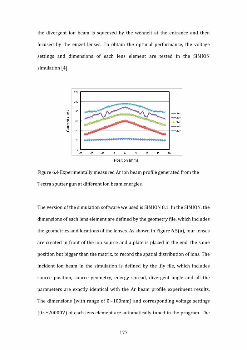
177
the divergent ion beam is squeezed by the wehnelt at the entrance and then
focused by the einzel lenses. To obtain the optimal performance, the voltage
settings and dimensions of each lens element are tested in the SIMION
simulation [4].
Figure 6.4 Experimentally measured Ar ion beam profile generated from the
Tectra sputter gun at different ion beam energies.
The version of the simulation software we used is SIMION 8.1. In the SIMION, the
dimensions of each lens element are defined by the geometry file, which includes
the geometries and locations of the lenses. As shown in Figure 6.5(a), four lenses
are created in front of the ion source and a plate is placed in the end, the same
position but bigger than the matrix, to record the spatial distribution of ions. The
incident ion beam in the simulation is defined by the .fly file, which includes
source position, source geometry, energy spread, divergent angle and all the
parameters are exactly identical with the Ar beam profile experiment results.
The dimensions (with range of 0~100mm) and corresponding voltage settings
(0~±20000V) of each lens element are automatically tuned in the program. The
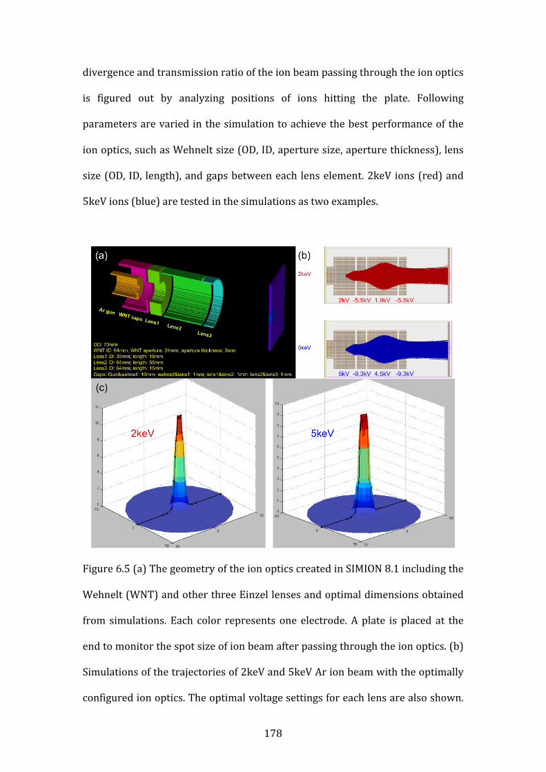
178
divergence and transmission ratio of the ion beam passing through the ion optics
is figured out by analyzing positions of ions hitting the plate. Following
parameters are varied in the simulation to achieve the best performance of the
ion optics, such as Wehnelt size (OD, ID, aperture size, aperture thickness), lens
size (OD, ID, length), and gaps between each lens element. 2keV ions (red) and
5keV ions (blue) are tested in the simulations as two examples.
Figure 6.5 (a) The geometry of the ion optics created in SIMION 8.1 including the
Wehnelt (WNT) and other three Einzel lenses and optimal dimensions obtained
from simulations. Each color represents one electrode. A plate is placed at the
end to monitor the spot size of ion beam after passing through the ion optics. (b)
Simulations of the trajectories of 2keV and 5keV Ar ion beam with the optimally
configured ion optics. The optimal voltage settings for each lens are also shown.
179
(c) Spatial distributions of the 2keV and 5keV Ar ions hitting on the matrix after
focused by the ion optics.
The optimal dimensions obtained from simulations are also shown in Figure
6.5(a), which is a balance of transmission ratio (>90%), focus (over 85% onto
matrix), required voltages (less than 10kV) and dimensions (less than 100mm in
order to fit in DN100CF flange). The trajectories of 2keV and 5keV ion beams
passing through the optimal ion optics configuration are shown in Figure 6.5(b).
The required voltages are also shown. The spot size of the Ar ions impinging on
the matrix (which is the final plate in the simulation) is recorded spatially and
the data analyzed in Matlab (by William Terry). The 3D plot of the spatial
distributions of Ar ions landing on the matrix at energies of 2keV and 5keV are
shown in Figure 6.5(c). The results obtained from the simulation show we are
able to focus over 85% ions onto matrix area (1 inch by 1 inch) with required
voltages less than 10kV.
6.1.7 Design of ion optics
The ion optics designed for the ion source are integrated on a DN100CF flange.
As shown in the schematic diagram in Figure 6.6 (a), two stainless steel rods are
fixed on the inner side of the flange to support the whole ion optics. For electrical
insulation, PTFE washers are used to mount the set of lenses on the supporting
rods. The designed ion optics were manufactured by the workshop based in
University of Birmingham and the assembled ion optics with ion source is shown
in Figure 6.6 (b-‐d). Each ion optic lens is connected to high voltage feedthroughs
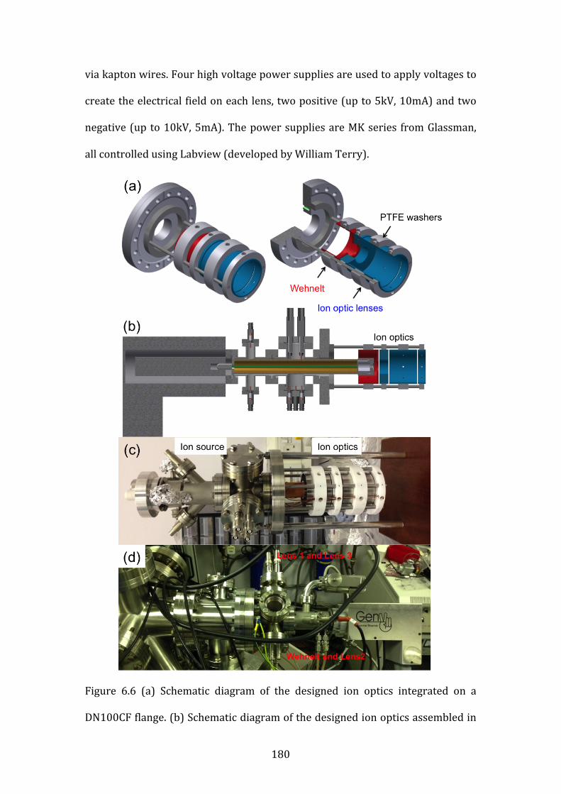
180
via kapton wires. Four high voltage power supplies are used to apply voltages to
create the electrical field on each lens, two positive (up to 5kV, 10mA) and two
negative (up to 10kV, 5mA). The power supplies are MK series from Glassman,
all controlled using Labview (developed by William Terry).
Figure 6.6 (a) Schematic diagram of the designed ion optics integrated on a
DN100CF flange. (b) Schematic diagram of the designed ion optics assembled in
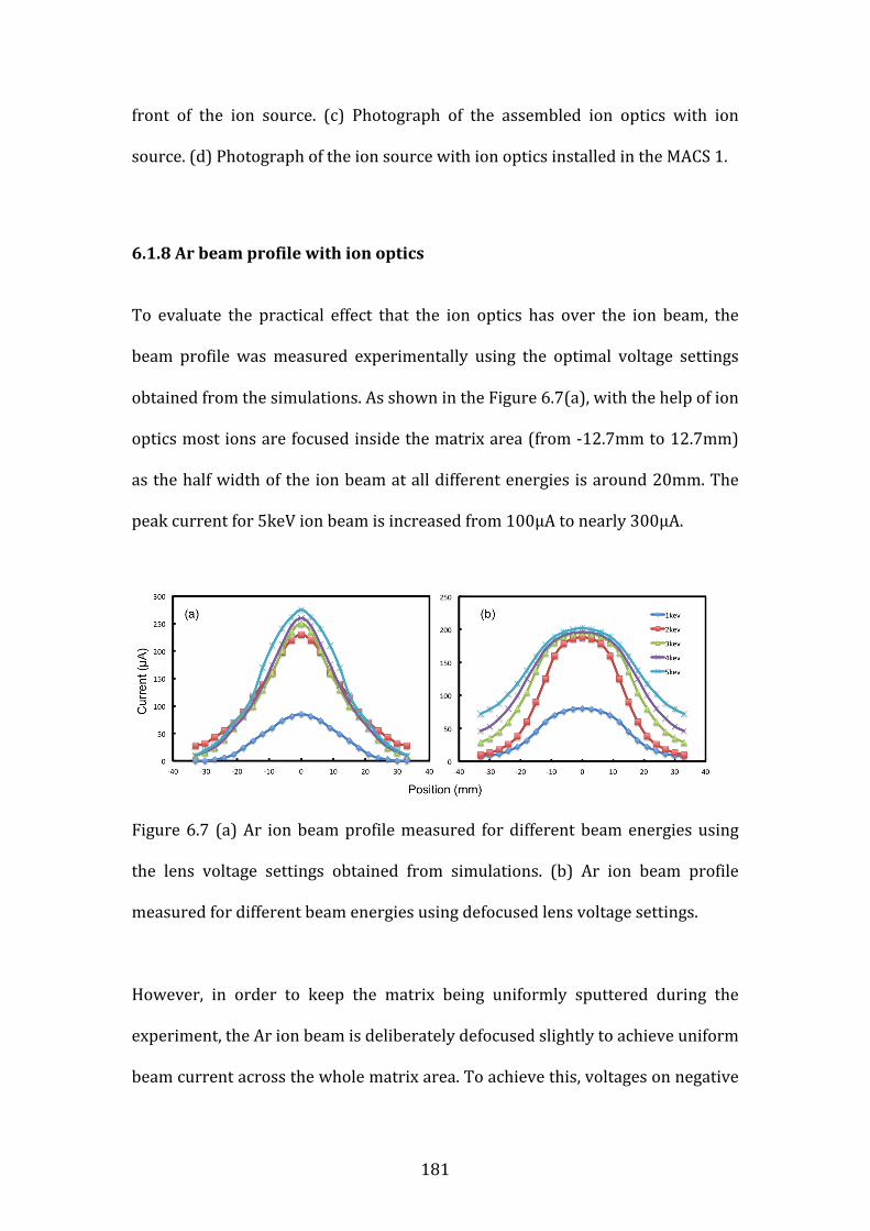
181
front of the ion source. (c) Photograph of the assembled ion optics with ion
source. (d) Photograph of the ion source with ion optics installed in the MACS 1.
6.1.8 Ar beam profile with ion optics
To evaluate the practical effect that the ion optics has over the ion beam, the
beam profile was measured experimentally using the optimal voltage settings
obtained from the simulations. As shown in the Figure 6.7(a), with the help of ion
optics most ions are focused inside the matrix area (from -‐12.7mm to 12.7mm)
as the half width of the ion beam at all different energies is around 20mm. The
peak current for 5keV ion beam is increased from 100μA to nearly 300μA.
Figure 6.7 (a) Ar ion beam profile measured for different beam energies using
the lens voltage settings obtained from simulations. (b) Ar ion beam profile
measured for different beam energies using defocused lens voltage settings.
However, in order to keep the matrix being uniformly sputtered during the
experiment, the Ar ion beam is deliberately defocused slightly to achieve uniform
beam current across the whole matrix area. To achieve this, voltages on negative
182
lenses are decreased about 5% and voltages on positive lenses are slightly tuned
up about 7%. The profile of Ar ion beam at the defocused settings is shown in
Figure 6.7(b).
6.2 Ag clusters produced in MACS 1
The performance of the MACS 1 was first tested by generating Ag clusters,
especially in terms of the cluster production rate and cluster size control. Similar
to the work conducted using the MACS demonstration system, the effects of
parameters such as evaporation speed, incident Ar ion beam current and energy
and matrix temperature on the cluster flux and size were systematically
investigated under more precise control and with a relatively larger range.
6.2.1 Cluster flux
The flux of clusters produced in the MACS 1 is measured from the density of
clusters deposited on the substrate within certain time. For this purpose, a
sample holder here contains an array of amorphous carbon film TEM grids was
installed as shown in Figure 6.8(a). The equivalent cluster flux is calculated
based on the average cluster density measured from HAADF STEM images times
multiplied by total production area and then divided by the deposition time. The
sample holder used here covers an area of 30mm by 30mm, which is
approximately the area of the matrix condensation support (1 inch by 1 inch). In
order to achieve the maximum cluster flux, the highest beam energy 5keV is used
to sputter the matrix as sputtering yield and maximum output beam current are
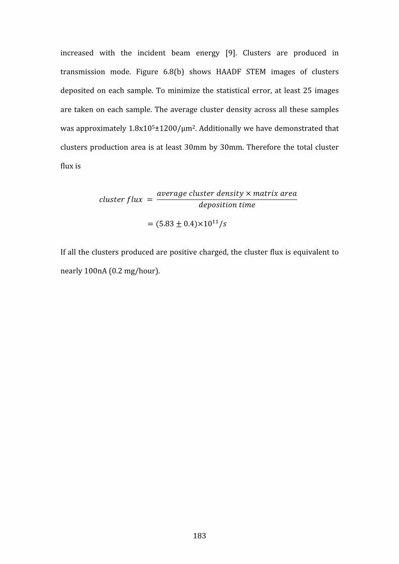
183
increased with the incident beam energy [9]. Clusters are produced in
transmission mode. Figure 6.8(b) shows HAADF STEM images of clusters
deposited on each sample. To minimize the statistical error, at least 25 images
are taken on each sample. The average cluster density across all these samples
was approximately 1.8x10⁵±1200/μm2. Additionally we have demonstrated that
clusters production area is at least 30mm by 30mm. Therefore the total cluster
flux is
𝑐𝑙𝑢𝑠𝑡𝑒𝑟 𝑓𝑙𝑢𝑥 = 𝑎𝑣𝑒𝑟𝑎𝑔𝑒 𝑐𝑙𝑢𝑠𝑡𝑒𝑟 𝑑𝑒𝑛𝑠𝑖𝑡𝑦 × 𝑚𝑎𝑡𝑟𝑖𝑥 𝑎𝑟𝑒𝑎
𝑑𝑒𝑝𝑜𝑠𝑖𝑡𝑖𝑜𝑛 𝑡𝑖𝑚𝑒
= (5.83± 0.4)×10!!/𝑠
If all the clusters produced are positive charged, the cluster flux is equivalent to
nearly 100nA (0.2 mg/hour).
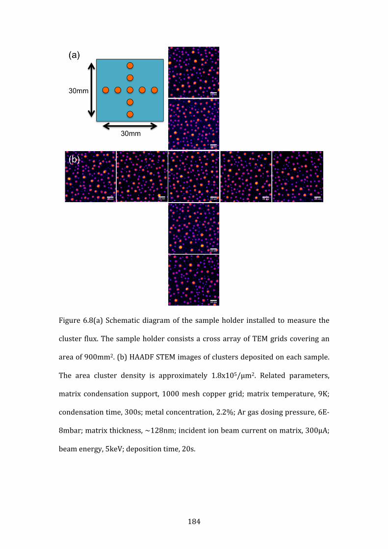
184
Figure 6.8(a) Schematic diagram of the sample holder installed to measure the
cluster flux. The sample holder consists a cross array of TEM grids covering an
area of 900mm2. (b) HAADF STEM images of clusters deposited on each sample.
The area cluster density is approximately 1.8x10⁵/μm2. Related parameters,
matrix condensation support, 1000 mesh copper grid; matrix temperature, 9K;
condensation time, 300s; metal concentration, 2.2%; Ar gas dosing pressure, 6E-‐
8mbar; matrix thickness, ~128nm; incident ion beam current on matrix, 300μA;
beam energy, 5keV; deposition time, 20s.
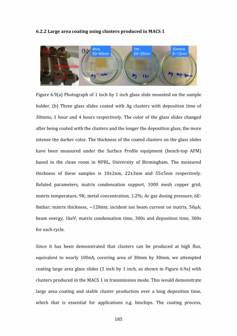
185
6.2.2 Large area coating using clusters produced in MACS 1
Figure 6.9(a) Photograph of 1 inch by 1 inch glass slide mounted on the sample
holder. (b) Three glass slides coated with Ag clusters with deposition time of
30mins, 1 hour and 4 hours respectively. The color of the glass slides changed
after being coated with the clusters and the longer the deposition glass, the more
intense the darker color. The thickness of the coated clusters on the glass slides
have been measured under the Surface Profile equipment (bench-‐top AFM)
based in the clean room in NPRL, University of Birmingham. The measured
thickness of these samples is 10±2nm, 22±3nm and 55±5nm respectively.
Related parameters, matrix condensation support, 1000 mesh copper grid;
matrix temperature, 9K; metal concentration, 1.2%; Ar gas dosing pressure, 6E-‐
8mbar; matrix thickness, ~128nm; incident ion beam current on matrix, 50μA;
beam energy, 1keV; matrix condensation time, 300s and deposition time, 300s
for each cycle.
Since it has been demonstrated that clusters can be produced at high flux,
equivalent to nearly 100nA, covering area of 30mm by 30mm, we attempted
coating large area glass slides (1 inch by 1 inch, as shown in Figure 6.9a) with
clusters produced in the MACS 1 in transmission mode. This would demonstrate
large area coating and stable cluster production over a long deposition time,
which that is essential for applications e.g. biochips. The coating process,
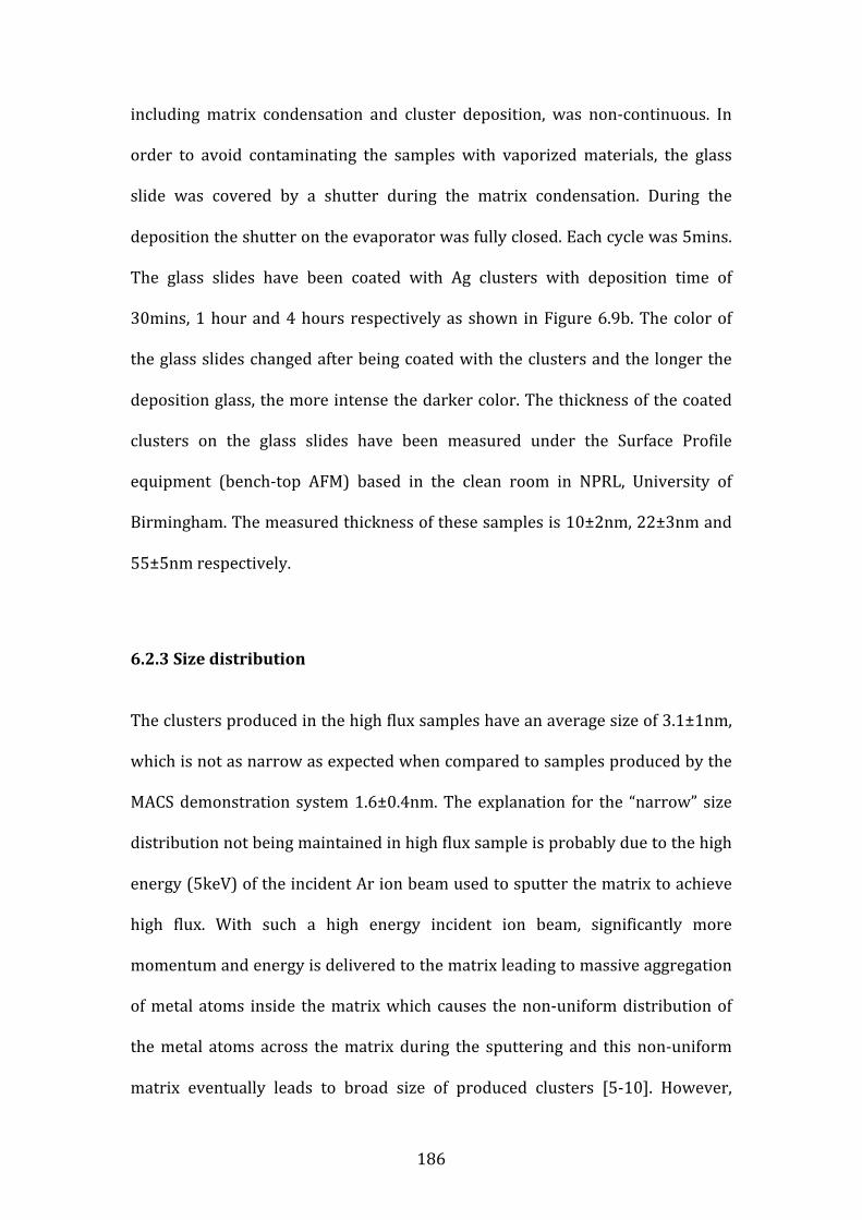
186
including matrix condensation and cluster deposition, was non-‐continuous. In
order to avoid contaminating the samples with vaporized materials, the glass
slide was covered by a shutter during the matrix condensation. During the
deposition the shutter on the evaporator was fully closed. Each cycle was 5mins.
The glass slides have been coated with Ag clusters with deposition time of
30mins, 1 hour and 4 hours respectively as shown in Figure 6.9b. The color of
the glass slides changed after being coated with the clusters and the longer the
deposition glass, the more intense the darker color. The thickness of the coated
clusters on the glass slides have been measured under the Surface Profile
equipment (bench-‐top AFM) based in the clean room in NPRL, University of
Birmingham. The measured thickness of these samples is 10±2nm, 22±3nm and
55±5nm respectively.
6.2.3 Size distribution
The clusters produced in the high flux samples have an average size of 3.1±1nm,
which is not as narrow as expected when compared to samples produced by the
MACS demonstration system 1.6±0.4nm. The explanation for the “narrow” size
distribution not being maintained in high flux sample is probably due to the high
energy (5keV) of the incident Ar ion beam used to sputter the matrix to achieve
high flux. With such a high energy incident ion beam, significantly more
momentum and energy is delivered to the matrix leading to massive aggregation
of metal atoms inside the matrix which causes the non-‐uniform distribution of
the metal atoms across the matrix during the sputtering and this non-‐uniform
matrix eventually leads to broad size of produced clusters [5-‐10]. However,
187
when lowering incident beam energy for example 1keV instead of 5keV, the
clusters exhibit “narrow” size distribution again as shown in Figure 6.10(a). The
size distribution measured from the integrated HAADF intensity of shown in
Figure 6.10(b).
Figure 6.10(a) HAADF STEM image and atomic resolution image of Ag clusters
prepared in MACS 1 using 1keV incident beam energy. All clusters in this image
have diameter of 2±0.5nm. (b) Histogram of size distribution of the Ag clusters.
The number of atoms is measured from the integrated HAADF intensity
comparing to the HAADF intensity of single atoms. The histogram shows the
clusters contain a average size of 250 atoms and half width of the distribution is
from about 150 to 350, which gives a mass resolution around M/ΔM=1.25.
Related parameters, matrix condensation support, 1000 mesh copper grid;
matrix temperature, 9K; condensation time, 200s; metal concentration, 1.2%; Ar
gas dosing pressure, 6E-‐8mbar; matrix thickness, ~85nm; incident ion beam
current on matrix, 50μA; beam energy, 1keV; deposition time, 120s.
As shown in the STEM image, all clusters in this image have a diameter of
2±0.5nm. The histogram of size distribution shows the clusters contain a average
size of 250 atoms and half width of the distribution is from about 150 to 350,
188
which gives a mass resolution around M/ΔM=1.25. More details of effects of
incident beam energy on cluster size will be discussed later in the effect of
incident beam energy part.
6.2.4 Size control
As preliminary demonstrated using the MACS demonstration apparatus, the size
of clusters can be controlled during the formation stage without any additional
mass selection. Results show cluster size is sensitive to several parameters,
especially the metal concentration in the matrix. This work was repeated in the
MACS 1 system but more systematically and with much better control of all the
parameters. HAADF STEM images (2Mx) and atomic resolution images (12Mx) of
Ag clusters prepared with different metal concentration (from 0.6% to 4.8%) are
shown in Figure 6.11(a). The corresponding histograms of cluster size
distribution measured from the integrated HAADF intensity are shown in Figure
6.11(b). The Gaussian function was used to fit the histograms of size distribution
in order to obtain the average sizes and size spreads. The cluster size and flux as
a function of metal concentration in the metal are plotted in Figure 6.11(c) and
(d) respectively.
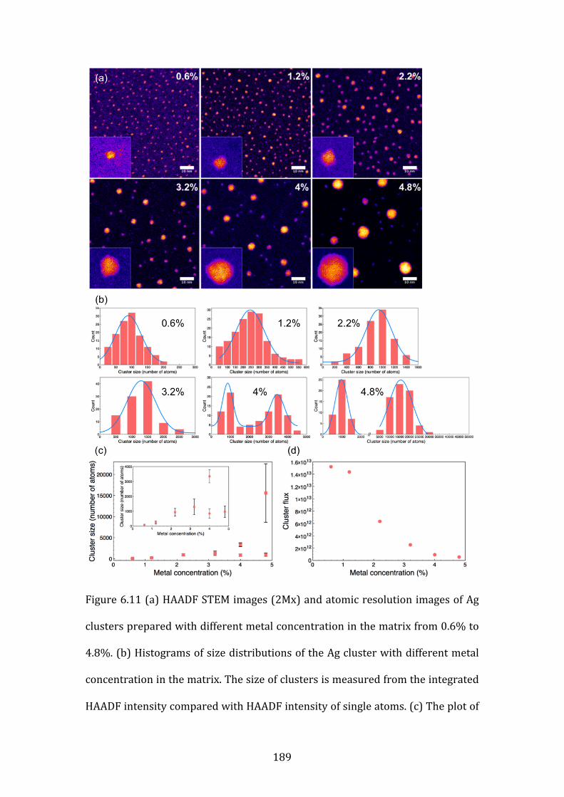
189
Figure 6.11 (a) HAADF STEM images (2Mx) and atomic resolution images of Ag
clusters prepared with different metal concentration in the matrix from 0.6% to
4.8%. (b) Histograms of size distributions of the Ag cluster with different metal
concentration in the matrix. The size of clusters is measured from the integrated
HAADF intensity compared with HAADF intensity of single atoms. (c) The plot of
190
size of clusters as a function of metal concentration. (d) The plot of cluster flux as
a function of metal concentration. The cluster flux is measured from the cluster
density on HAADF STEM images. Related parameters, matrix condensation
support, 1000 mesh copper grid; matrix temperature, 9K; condensation time,
200s; Ar gas dosing pressure, 6E-‐8mbar; matrix thickness, ~85nm; incident ion
beam current on matrix, 50μA; beam energy, 1keV; deposition time, 120s.
As mentioned before, the cluster formation in the MACS is possibly through two
mechanisms: clusters preformed due to the potential force [11-‐14] and
aggregated because of the ion impacts [15-‐23]. With higher metal concentration
in the matrix, clusters formed in both mechanisms are grown larger by capturing
more atoms, as there is a higher density of cluster material atoms when metal
concentration is high. However, the effects of the metal concentration on each
formation mechanism have different levels. The clusters formed driven by
potential force have limited mean free path that they are only able to capture
atoms within few angstroms (as simulated by Dr. Lanqing Xu). While the clusters
formed due to the aggregation under ion impacts are more energetic that larger
clusters are more likely to be formed with the help of ion-‐induced diffusion. This
difference leads to the spread size distribution of clusters prepared at higher
metal concentration matrix (4% and 4.8%). The trend of total cluster flux
decreases as a function of metal loading percentage in the matrix is probably due
to the fact that heavier metal loaded matrix is hard to sputter and has a lower
sputtering yield [5-‐10].
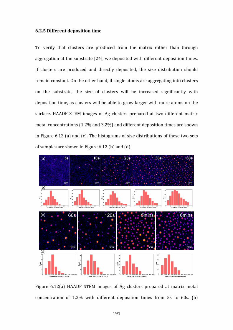
191
6.2.5 Different deposition time
To verify that clusters are produced from the matrix rather than through
aggregation at the substrate [24], we deposited with different deposition times.
If clusters are produced and directly deposited, the size distribution should
remain constant. On the other hand, if single atoms are aggregating into clusters
on the substrate, the size of clusters will be increased significantly with
deposition time, as clusters will be able to grow larger with more atoms on the
surface. HAADF STEM images of Ag clusters prepared at two different matrix
metal concentrations (1.2% and 3.2%) and different deposition times are shown
in Figure 6.12 (a) and (c). The histograms of size distributions of these two sets
of samples are shown in Figure 6.12 (b) and (d).
Figure 6.12(a) HAADF STEM images of Ag clusters prepared at matrix metal
concentration of 1.2% with different deposition times from 5s to 60s. (b)
192
Histograms of size distribution of the produced Ag clusters. (c) HAADF STEM
images of Ag clusters prepared at matrix metal concentration of 3.2% with
different deposition times from 60s to 6mins. (d) Histograms of size distribution
of the produced Ag clusters. The size of clusters is measured from the integrated
HAADF intensity compared to the HAADF intensity of single atoms. Related
parameters, matrix condensation support, 1000 mesh copper grid; matrix
temperature, 9K; condensation time, 300s; Ar gas dosing pressure, 6E-‐8mbar;
matrix thickness, ~128nm; incident ion beam current on matrix, 50μA; beam
energy, 1keV.
As shown in the HAADF STEM images and histograms of size distributions, the
size of clusters prepared at both matrix metal concentration remains the same
with different deposition time and the size distributions are quite similar.
However, the distribution does shift slightly towards larger size as the
deposition time increases due to clusters landing on top of each other with such
high density. The results provide indirect evidence that the clusters are
produced from the matrix rather than from single atoms aggregation. The direct
proof is taking mass spectra of the clusters that will be discussed in mass spectra
part.
6.3 Au clusters produced in MACS 1
Similar to the work done on Ag clusters, effects of different parameters (metal
concentration, incident beam energy, matrix temperature etc.) on size and flux of
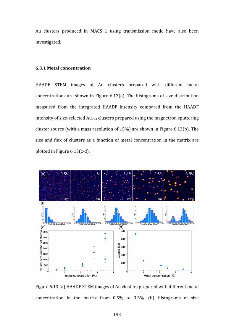
193
Au clusters produced in MACS 1 using transmission mode have also been
investigated.
6.3.1 Metal concentration
HAADF STEM images of Au clusters prepared with different metal
concentrations are shown in Figure 6.13(a). The histograms of size distribution
measured from the integrated HAADF intensity compared from the HAADF
intensity of size-‐selected Au923 clusters prepared using the magnetron sputtering
cluster source (with a mass resolution of ±5%) are shown in Figure 6.13(b). The
size and flux of clusters as a function of metal concentration in the matrix are
plotted in Figure 6.13(c-‐d).
Figure 6.13 (a) HAADF STEM images of Au clusters prepared with different metal
concentration in the matrix from 0.5% to 3.5%. (b) Histograms of size
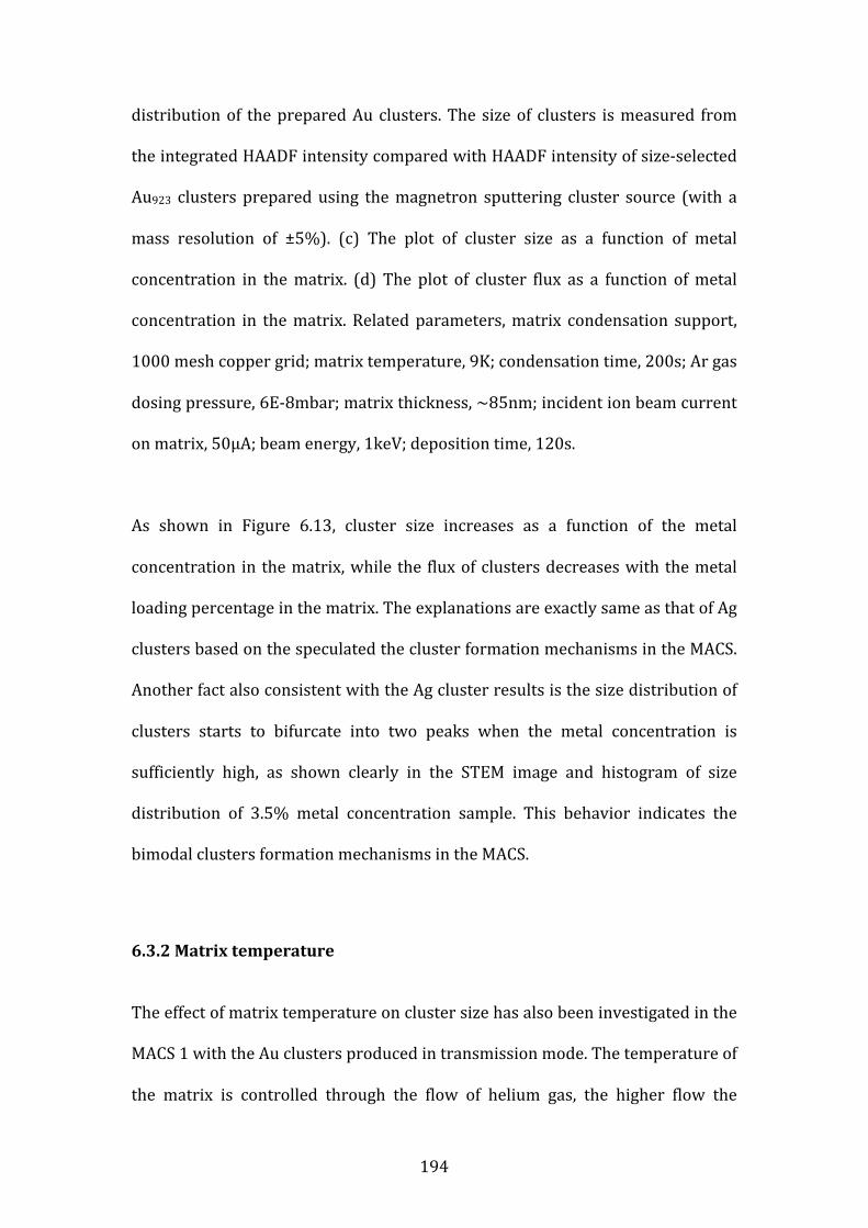
194
distribution of the prepared Au clusters. The size of clusters is measured from
the integrated HAADF intensity compared with HAADF intensity of size-‐selected
Au923 clusters prepared using the magnetron sputtering cluster source (with a
mass resolution of ±5%). (c) The plot of cluster size as a function of metal
concentration in the matrix. (d) The plot of cluster flux as a function of metal
concentration in the matrix. Related parameters, matrix condensation support,
1000 mesh copper grid; matrix temperature, 9K; condensation time, 200s; Ar gas
dosing pressure, 6E-‐8mbar; matrix thickness, ~85nm; incident ion beam current
on matrix, 50μA; beam energy, 1keV; deposition time, 120s.
As shown in Figure 6.13, cluster size increases as a function of the metal
concentration in the matrix, while the flux of clusters decreases with the metal
loading percentage in the matrix. The explanations are exactly same as that of Ag
clusters based on the speculated the cluster formation mechanisms in the MACS.
Another fact also consistent with the Ag cluster results is the size distribution of
clusters starts to bifurcate into two peaks when the metal concentration is
sufficiently high, as shown clearly in the STEM image and histogram of size
distribution of 3.5% metal concentration sample. This behavior indicates the
bimodal clusters formation mechanisms in the MACS.
6.3.2 Matrix temperature
The effect of matrix temperature on cluster size has also been investigated in the
MACS 1 with the Au clusters produced in transmission mode. The temperature of
the matrix is controlled through the flow of helium gas, the higher flow the
195
higher cooling power and therefore lower temperature. The temperature of the
matrix fluctuates less than 1K during experiments. HAADF STEM images of Au
clusters prepared with four different matrix temperatures from 9K to 22K are
shown in Figure 6.14(a). The histograms of size distribution are shown in Figure
6.14(b).
Figure 6.14 (a) HAADF STEM images of Au clusters prepared with different
matrix temperature from 9K to 22K. The temperature of the matrix fluctuates
less than 1K during experiments. (b) The histograms of size distribution of the
Au clusters. The number of atoms in cluster is measured from the integrated
HAADF intensity compared with the HAADF intensity of mass balance, the size-‐
selected Au923 prepared in the magnetron sputtering source. Related parameters,
matrix condensation support, 1000 mesh copper grid; condensation time, 200s;
metal concentration, 2.8%; Ar gas dosing pressure, 6E-‐8mbar; matrix thickness,
~85nm; incident ion beam current on matrix, 50μA; beam energy, 1keV;
deposition time, 120s.
196
As shown in the STEM images and the histograms of the size distributions, the
distribution shifts to smaller sizes with the increased matrix temperature. The
explanation to this phenomenon is not quite clear yet. We propose that the
matrix temperature affects the following conditions: sputtering yield of the
matrix, mobility of atoms in the matrix and the sticking co-‐efficient of the
condensed atoms. The effect on the sputtering yield is mainly attributed to the
thermal spike that atoms in a warmer matrix require less energy to eject [25-‐26].
The mobility of atoms affected by matrix temperature can be described by
kinetic energy and Brownian motion [27]. For simplicity, the sticking co-‐efficient
is treated as 1. Although metal atoms are more mobile in a warmer matrix
intended to form larger clusters, they are more easily ejected from the matrix
during ion bombardment as requiring less energy, meaning the clusters have less
“germination time” (the time allowing cluster growth before leaving the matrix).
6.3.3 Effect of incident beam energy
Here, we varied the incident beam energy from 1keV to 4keV to study the effect
of beam energy on Au cluster size and flux in transmission mode. HAADF STEM
images of Au clusters prepared with different incident beam energy are shown in
Figure 6.15(a) and the histograms of size distribution are shown in Figure
6.15(b).
As shown in the both STEM images and the histogram of size distributions, the
size of clusters, both average and maximum size, is increased with the incident
beam energy. However on the other hand, the size distribution becomes broader
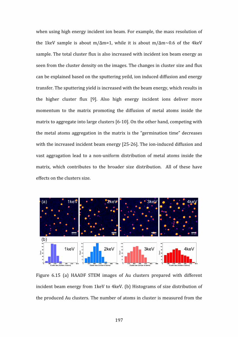
197
when using high energy incident ion beam. For example, the mass resolution of
the 1keV sample is about m/Δm=1, while it is about m/Δm~0.6 of the 4keV
sample. The total cluster flux is also increased with incident ion beam energy as
seen from the cluster density on the images. The changes in cluster size and flux
can be explained based on the sputtering yeild, ion induced diffusion and energy
transfer. The sputtering yield is increased with the beam energy, which results in
the higher cluster flux [9]. Also high energy incident ions deliver more
momentum to the matrix promoting the diffusion of metal atoms inside the
matrix to aggregate into large clusters [6-‐10]. On the other hand, competing with
the metal atoms aggregation in the matrix is the “germination time” decreases
with the increased incident beam energy [25-‐26]. The ion-‐induced diffusion and
vast aggragation lead to a non-‐uniform distribution of metal atoms inside the
matrix, which contributes to the broader size distribution. All of these have
effects on the clusters size.
Figure 6.15 (a) HAADF STEM images of Au clusters prepared with different
incident beam energy from 1keV to 4keV. (b) Histograms of size distribution of
the produced Au clusters. The number of atoms in cluster is measured from the
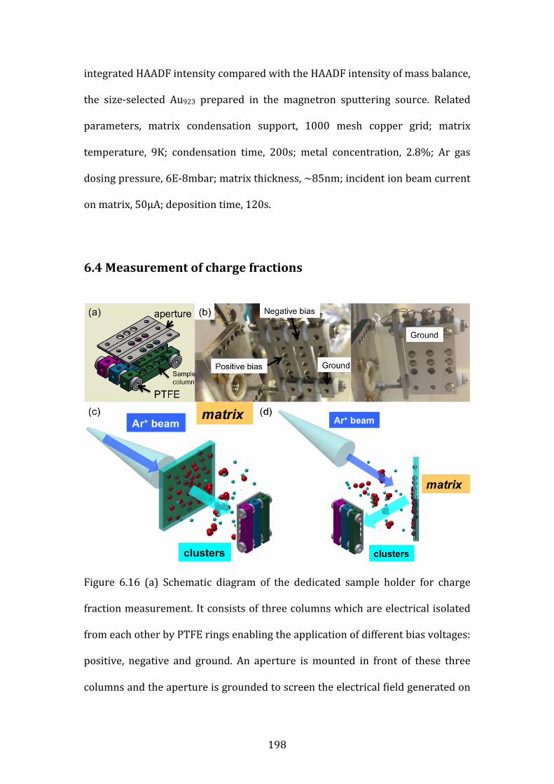
198
integrated HAADF intensity compared with the HAADF intensity of mass balance,
the size-‐selected Au923 prepared in the magnetron sputtering source. Related
parameters, matrix condensation support, 1000 mesh copper grid; matrix
temperature, 9K; condensation time, 200s; metal concentration, 2.8%; Ar gas
dosing pressure, 6E-‐8mbar; matrix thickness, ~85nm; incident ion beam current
on matrix, 50μA; deposition time, 120s.
6.4 Measurement of charge fractions
Figure 6.16 (a) Schematic diagram of the dedicated sample holder for charge
fraction measurement. It consists of three columns which are electrical isolated
from each other by PTFE rings enabling the application of different bias voltages:
positive, negative and ground. An aperture is mounted in front of these three
columns and the aperture is grounded to screen the electrical field generated on
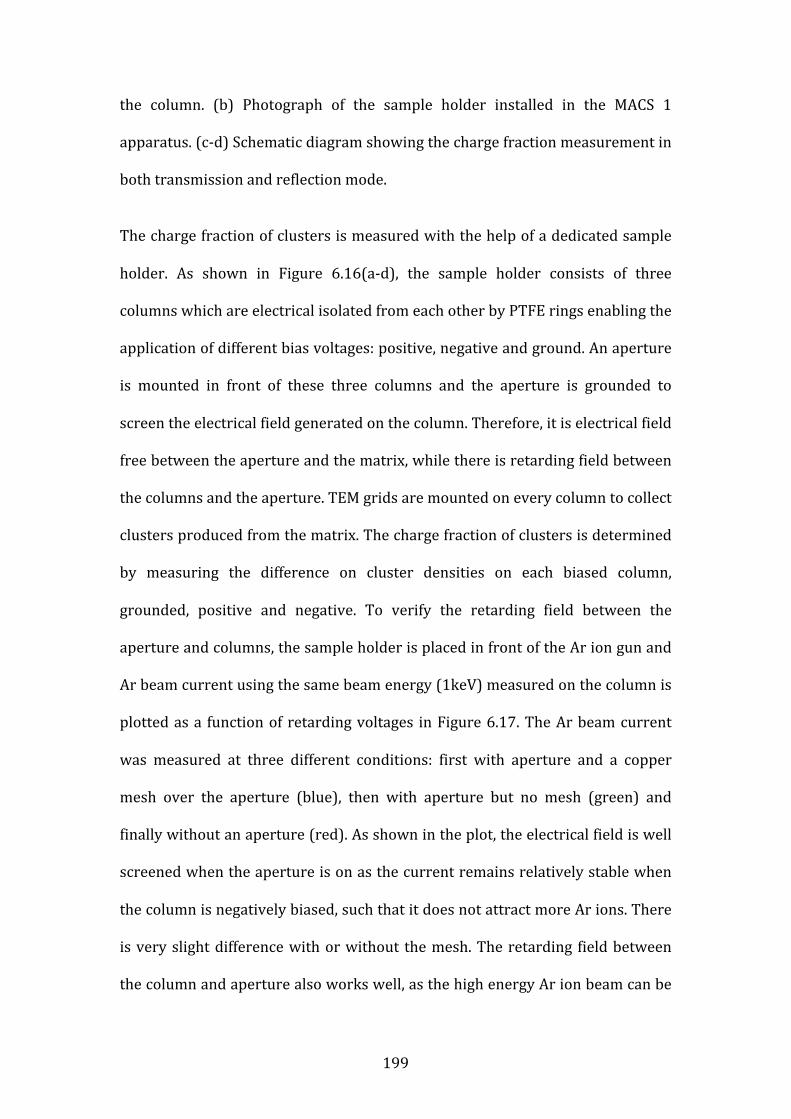
199
the column. (b) Photograph of the sample holder installed in the MACS 1
apparatus. (c-‐d) Schematic diagram showing the charge fraction measurement in
both transmission and reflection mode.
The charge fraction of clusters is measured with the help of a dedicated sample
holder. As shown in Figure 6.16(a-‐d), the sample holder consists of three
columns which are electrical isolated from each other by PTFE rings enabling the
application of different bias voltages: positive, negative and ground. An aperture
is mounted in front of these three columns and the aperture is grounded to
screen the electrical field generated on the column. Therefore, it is electrical field
free between the aperture and the matrix, while there is retarding field between
the columns and the aperture. TEM grids are mounted on every column to collect
clusters produced from the matrix. The charge fraction of clusters is determined
by measuring the difference on cluster densities on each biased column,
grounded, positive and negative. To verify the retarding field between the
aperture and columns, the sample holder is placed in front of the Ar ion gun and
Ar beam current using the same beam energy (1keV) measured on the column is
plotted as a function of retarding voltages in Figure 6.17. The Ar beam current
was measured at three different conditions: first with aperture and a copper
mesh over the aperture (blue), then with aperture but no mesh (green) and
finally without an aperture (red). As shown in the plot, the electrical field is well
screened when the aperture is on as the current remains relatively stable when
the column is negatively biased, such that it does not attract more Ar ions. There
is very slight difference with or without the mesh. The retarding field between
the column and aperture also works well, as the high energy Ar ion beam can be
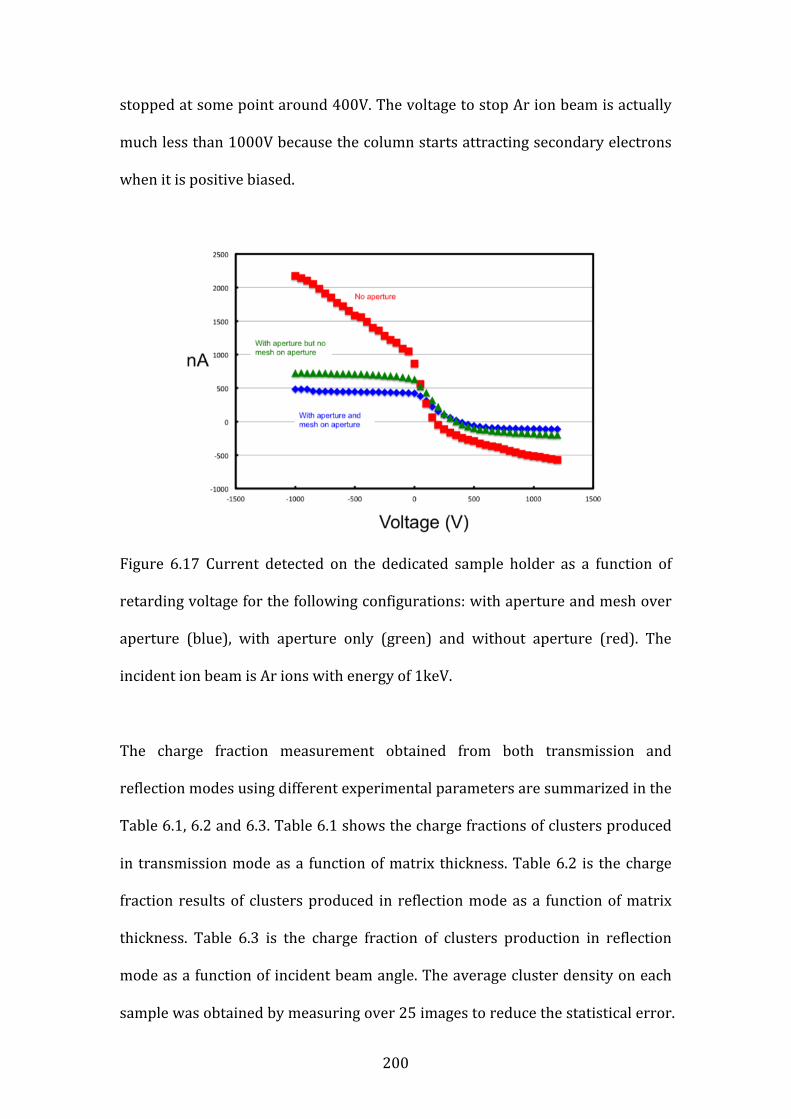
200
stopped at some point around 400V. The voltage to stop Ar ion beam is actually
much less than 1000V because the column starts attracting secondary electrons
when it is positive biased.
Figure 6.17 Current detected on the dedicated sample holder as a function of
retarding voltage for the following configurations: with aperture and mesh over
aperture (blue), with aperture only (green) and without aperture (red). The
incident ion beam is Ar ions with energy of 1keV.
The charge fraction measurement obtained from both transmission and
reflection modes using different experimental parameters are summarized in the
Table 6.1, 6.2 and 6.3. Table 6.1 shows the charge fractions of clusters produced
in transmission mode as a function of matrix thickness. Table 6.2 is the charge
fraction results of clusters produced in reflection mode as a function of matrix
thickness. Table 6.3 is the charge fraction of clusters production in reflection
mode as a function of incident beam angle. The average cluster density on each
sample was obtained by measuring over 25 images to reduce the statistical error.
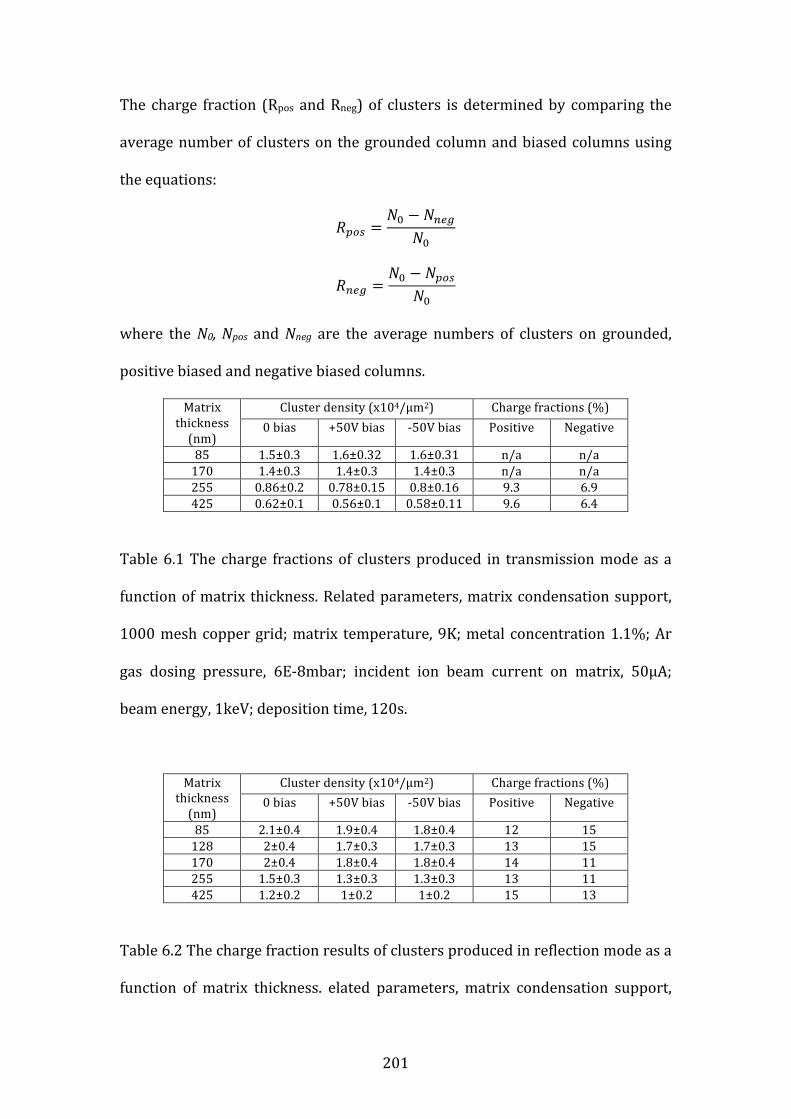
201
The charge fraction (Rpos and Rneg) of clusters is determined by comparing the
average number of clusters on the grounded column and biased columns using
the equations:
𝑅!"# =𝑁! − 𝑁!"#
𝑁!
𝑅!"# =𝑁! − 𝑁!"#
𝑁!
where the N0, Npos and Nneg are the average numbers of clusters on grounded,
positive biased and negative biased columns.
Matrix thickness (nm)
Cluster density (x104/μm2) Charge fractions (%) 0 bias +50V bias -‐50V bias Positive Negative
85 1.5±0.3 1.6±0.32 1.6±0.31 n/a n/a 170 1.4±0.3 1.4±0.3 1.4±0.3 n/a n/a 255 0.86±0.2 0.78±0.15 0.8±0.16 9.3 6.9 425 0.62±0.1 0.56±0.1 0.58±0.11 9.6 6.4
Table 6.1 The charge fractions of clusters produced in transmission mode as a
function of matrix thickness. Related parameters, matrix condensation support,
1000 mesh copper grid; matrix temperature, 9K; metal concentration 1.1%; Ar
gas dosing pressure, 6E-‐8mbar; incident ion beam current on matrix, 50μA;
beam energy, 1keV; deposition time, 120s.
Matrix thickness (nm)
Cluster density (x104/μm2) Charge fractions (%) 0 bias +50V bias -‐50V bias Positive Negative
85 2.1±0.4 1.9±0.4 1.8±0.4 12 15 128 2±0.4 1.7±0.3 1.7±0.3 13 15 170 2±0.4 1.8±0.4 1.8±0.4 14 11 255 1.5±0.3 1.3±0.3 1.3±0.3 13 11 425 1.2±0.2 1±0.2 1±0.2 15 13
Table 6.2 The charge fraction results of clusters produced in reflection mode as a
function of matrix thickness. elated parameters, matrix condensation support,
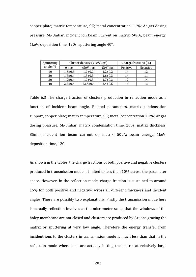
202
copper plate; matrix temperature, 9K; metal concentration 1.1%; Ar gas dosing
pressure, 6E-‐8mbar; incident ion beam current on matrix, 50μA; beam energy,
1keV; deposition time, 120s; sputtering angle 40°.
Sputtering angle (°)
Cluster density (x104/μm2) Charge fractions (%) 0 bias +50V bias -‐50V bias Positive Negative
10 1.3±0.3 1.2±0.2 1.2±0.2 14 12 20 1.8±0.4 1.5±0.3 1.6±0.3 14 11 30 1.9±0.4 1.7±0.3 1.7±0.3 12 14 40 2.7±0.5 12.3±0.4 2.4±0.5 16 13
Table 6.3 The charge fraction of clusters production in reflection mode as a
function of incident beam angle. Related parameters, matrix condensation
support, copper plate; matrix temperature, 9K; metal concentration 1.1%; Ar gas
dosing pressure, 6E-‐8mbar; matrix condensation time, 200s; matrix thickness,
85nm; incident ion beam current on matrix, 50μA; beam energy, 1keV;
deposition time, 120.
As shown in the tables, the charge fractions of both positive and negative clusters
produced in transmission mode is limited to less than 10% across the parameter
space. However, in the reflection mode, charge fraction is sustained to around
15% for both positive and negative across all different thickness and incident
angles. There are possibly two explanations. Firstly the transmission mode here
is actually reflection involves at the micrometer scale, that the windows of the
holey membrane are not closed and clusters are produced by Ar ions grazing the
matrix or sputtering at very low angle. Therefore the energy transfer from
incident ions to the clusters in transmission mode is much less than that in the
reflection mode where ions are actually hitting the matrix at relatively large
203
angle [28-‐30], resulting in less ionization. Another possibility is the Ar matrix is
not a good electrical conductor and it might be charged during the Ar ion beam
sputtering. Clusters produced in the transmission mode are formed inside the
micro-‐channels and are travelling through the channel before landing onto the
substrate. If the matrix is charged but not uniformly charged, an electrical field
will be created inside those channels which may deflect and stop the charged
clusters flying out. While in the reflection mode there is no such obstruction after
clusters are released out of the matrix [31-‐32].
6.5 Mass spectroscopy of clusters produced in the MACS
6.5.1 Experiment setup
The lateral time-‐of-‐flight mass filter is attached to the MACS 1 in order to acquire
mass spectra as shown in Figure 6.18. The clusters are produced in the reflection
mode as the charge fraction is higher than that of the transmission mode. A set of
ion optic lenses with an XY deflector are built in between the cluster generation
chamber and the mass filter to extract and focus clusters through. The
orientation of the matrix is 45 degree from the incident beam direction. In order
to prevent the ion optic lenses shorting from the vaporized metal, a metal case
has been designed to protect the lenses as well as screen the electrical field
around the outside of the ion optic lenses.
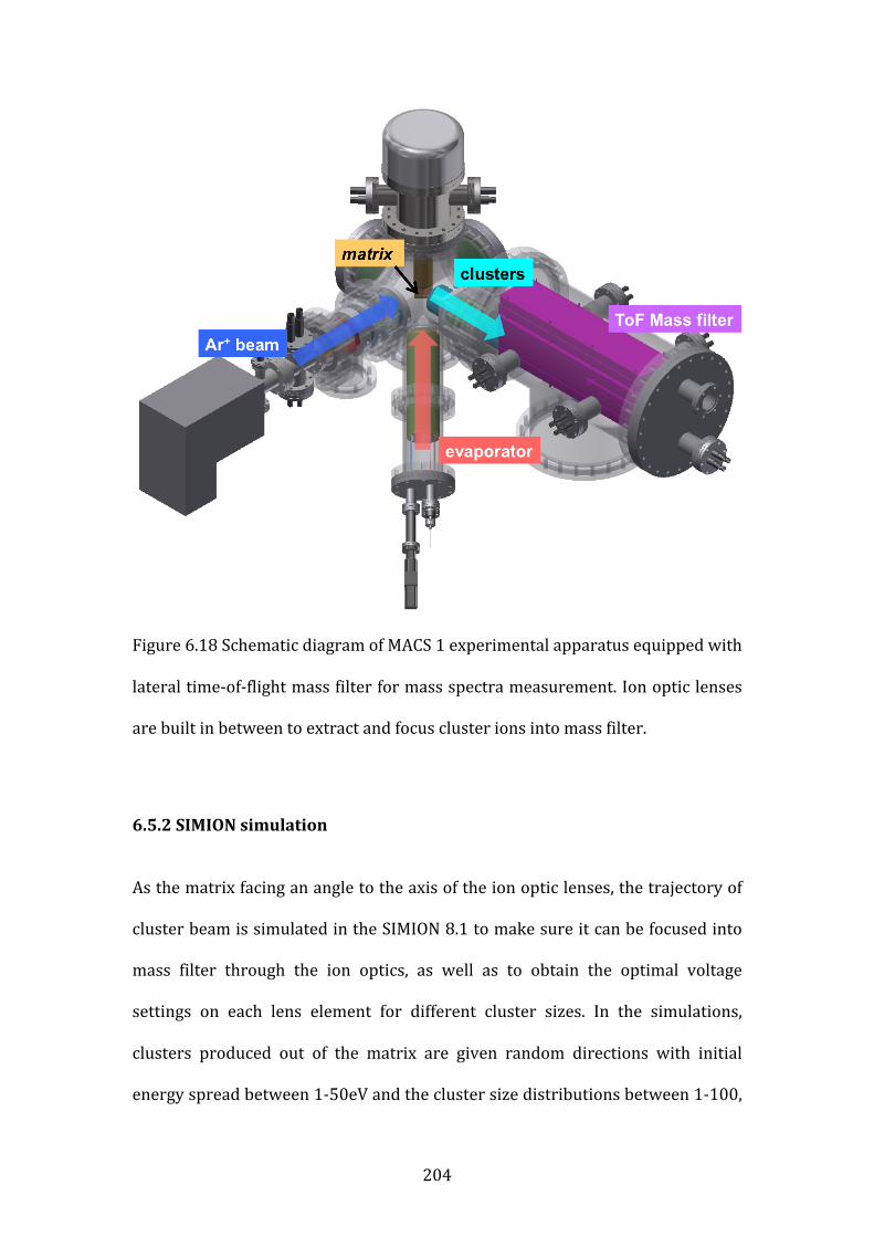
204
Figure 6.18 Schematic diagram of MACS 1 experimental apparatus equipped with
lateral time-‐of-‐flight mass filter for mass spectra measurement. Ion optic lenses
are built in between to extract and focus cluster ions into mass filter.
6.5.2 SIMION simulation
As the matrix facing an angle to the axis of the ion optic lenses, the trajectory of
cluster beam is simulated in the SIMION 8.1 to make sure it can be focused into
mass filter through the ion optics, as well as to obtain the optimal voltage
settings on each lens element for different cluster sizes. In the simulations,
clusters produced out of the matrix are given random directions with initial
energy spread between 1-‐50eV and the cluster size distributions between 1-‐100,
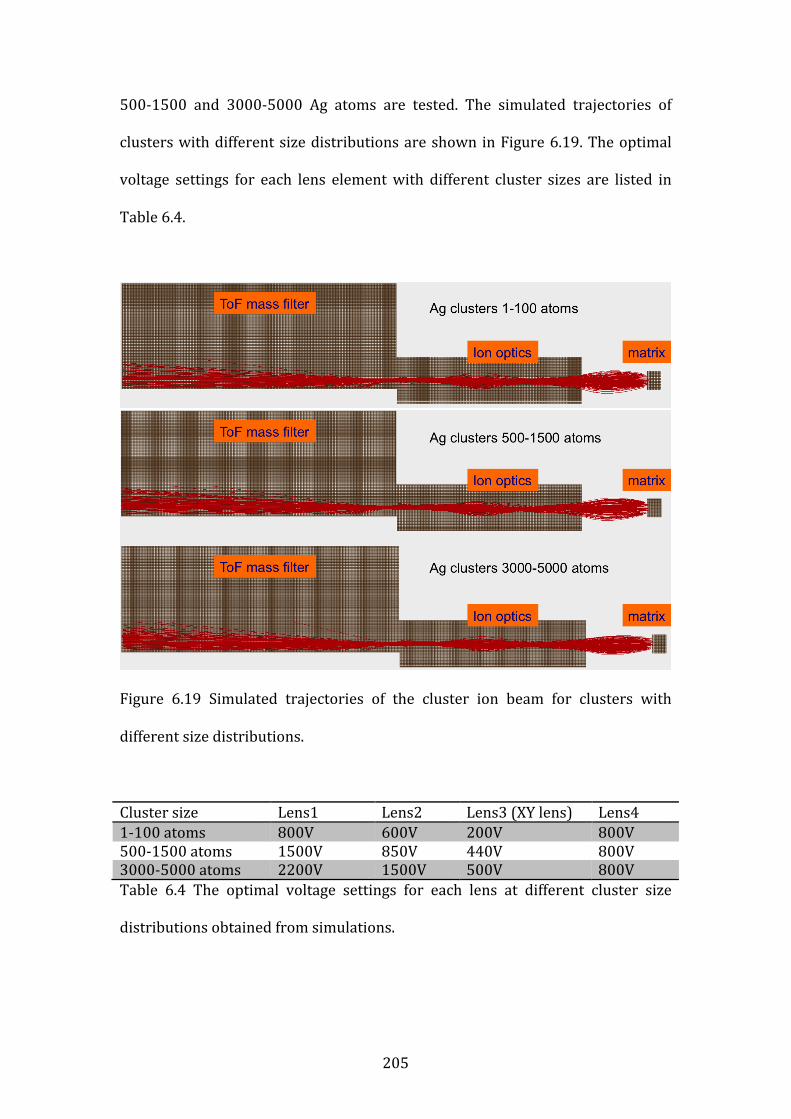
205
500-‐1500 and 3000-‐5000 Ag atoms are tested. The simulated trajectories of
clusters with different size distributions are shown in Figure 6.19. The optimal
voltage settings for each lens element with different cluster sizes are listed in
Table 6.4.
Figure 6.19 Simulated trajectories of the cluster ion beam for clusters with
different size distributions.
Cluster size Lens1 Lens2 Lens3 (XY lens) Lens4 1-‐100 atoms 800V 600V 200V 800V 500-‐1500 atoms 1500V 850V 440V 800V 3000-‐5000 atoms 2200V 1500V 500V 800V Table 6.4 The optimal voltage settings for each lens at different cluster size
distributions obtained from simulations.
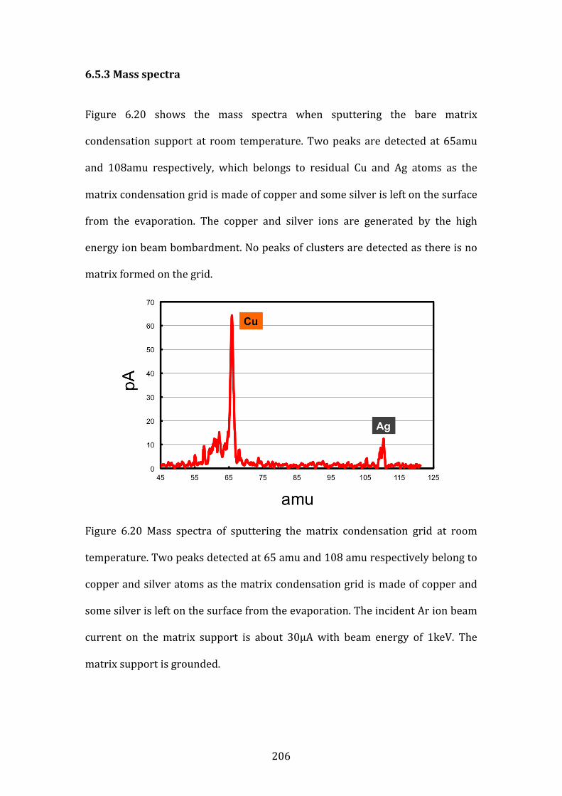
206
6.5.3 Mass spectra
Figure 6.20 shows the mass spectra when sputtering the bare matrix
condensation support at room temperature. Two peaks are detected at 65amu
and 108amu respectively, which belongs to residual Cu and Ag atoms as the
matrix condensation grid is made of copper and some silver is left on the surface
from the evaporation. The copper and silver ions are generated by the high
energy ion beam bombardment. No peaks of clusters are detected as there is no
matrix formed on the grid.
Figure 6.20 Mass spectra of sputtering the matrix condensation grid at room
temperature. Two peaks detected at 65 amu and 108 amu respectively belong to
copper and silver atoms as the matrix condensation grid is made of copper and
some silver is left on the surface from the evaporation. The incident Ar ion beam
current on the matrix support is about 30μA with beam energy of 1keV. The
matrix support is grounded.
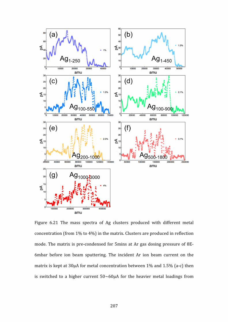
207
Figure 6.21 The mass spectra of Ag clusters produced with different metal
concentration (from 1% to 4%) in the matrix. Clusters are produced in reflection
mode. The matrix is pre-‐condensed for 5mins at Ar gas dosing pressure of 8E-‐
6mbar before ion beam sputtering. The incident Ar ion beam current on the
matrix is kept at 30μA for metal concentration between 1% and 1.5% (a-‐c) then
is switched to a higher current 50~60μA for the heavier metal loadings from
208
2.1% to 4% (d-‐g) to get a better signal. The beam energy is kept at 1keV and
matrix support is grounded.
The mass spectra of Ag clusters produced with different metal concentration
(from 1% to 4%) in the matrix are shown in Figure 6.21. The size ranges of
clusters detected at different metal concentrations are also marked in the mass
spectra. The mass spectra measurement of the clusters directly demonstrates the
proof-‐of-‐principle of the MACS technology. The variations in the mass spectra
such as cluster size, size distribution and flux at different metal concentration
are also consistent with the STEM results discussed previously. Please be aware
the peaks observed in all the mass spectra shown above are not referring to the
magic numbers. Instead they are more likely the fluctuations due to the unstable
incident ion beam current or charging and discharging of the matrix.
6.6 Summary
In this chapter, the design and operation of a new experimental setup of the
MACS system, the MACS 1, to scale up the cluster production rate has been
discussed. The MACS allows further exploration of the effects of different
experimental parameters on cluster size and flux. The cluster flux we have
achieved in the MACS 1 is equivalent to nearly 100nA of Ag clusters produced
from the 1-‐inch by 1-‐inch matrix in transmission mode. The effects of metal
concentration in the matrix, incident beam energy and deposition time on both
Ag and Au cluster size and flux have been investigated. The charge fractions of
the clusters are also studied, with charged fractions of <10% and <15% for

209
transmission and reflection mode, respectively. Mass spectra are obtained from
the charged clusters using lateral time-‐of-‐flight mass selector, further confirming
the cluster production and size control in the MACS.
210
List of references
[1] Anton, R., et al. "Design and performance of a versatile, cost-‐effective
microwave electron cyclotron resonance plasma source for surface and thin film
processing." Review of Scientific Instruments 71.2 (2000): 1177-‐1180.
[2] Baxter, William J., and Stanley R. Rouze. "A photoemission electron
microscope using an electron multiplier array." Review of Scientific
Instruments44.11 (1973): 1628-‐1629.
[3] Stefanaki, Eleni-‐Chrysanthi. "Electron Microscope: The Basics."
[4] Dahl, David A. "SIMION for the personal computer in reflection." International
Journal of Mass Spectrometry 200.1 (2000): 3-‐25.
[5] Balaji, V., et al. "Sputtering yields of condensed rare gases." Nuclear
Instruments and Methods in Physics Research Section B: Beam Interactions with
Materials and Atoms 46.1 (1990): 435-‐440.
[6] Makeev, Maxim A., and Albert-‐László Barabási. "Ion-‐induced effective surface
diffusion in ion sputtering." Applied physics letters 71.19 (1997): 2800-‐2802.
[7] Babaev, V. O., Ju V. Bykov, and M. B. Guseva. "Effect of ion irradiation on the
formation, structure and properties of thin metal films." Thin Solid Films 38.1
(1976): 1-‐8.
[8] Marinov, Miko. "Effect of ion bombardment on the initial stages of thin film
growth." Thin Solid Films 46.3 (1977): 267-‐274.
[9] MacLaren, S. W., et al. "Surface roughness development during sputtering of
GaAs and InP: Evidence for the role of surface diffusion in ripple formation and
sputter cone development." Journal of Vacuum Science & Technology A 10.3
(1992): 468-‐476.
211
[10] Cavaille, J. Y., and M. Drechsler. "Surface self-‐diffusion by ion
impact." Surface Science 75.2 (1978): 342-‐354.
[11] Silvera, Isaac F., and Victor V. Goldman. "The isotropic intermolecular
potential for H2 and D2 in the solid and gas phases." The Journal of Chemical
Physics 69.9 (1978): 4209-‐4213.
[12] Mirsky, Kira. "Carbon monoxide molecules in an argon matrix: empirical
evaluation of the Ar· Ar, C· Ar and O· Ar potential parameters." Chemical Physics
46.3 (1980): 445-‐455.
[13] Tang, K. T., and J. Peter Toennies. "New combining rules for well parameters
and shapes of the van der Waals potential of mixed rare gas systems." Zeitschrift
für Physik D Atoms, Molecules and Clusters 1.1 (1986): 91-‐101.
[14] Mann, D. E., N. Acquista, and David White. "Infrared Spectra of HCl, DCl, HBr,
and DBr in Solid Rare‐Gas Matrices." The Journal of Chemical Physics 44.9
(1966): 3453-‐3467.
[15] Makeev, Maxim A., and Albert-‐László Barabási. "Ion-‐induced effective
surface diffusion in ion sputtering." Applied physics letters 71.19 (1997): 2800-‐
2802.
[16] Winters, Harold F., et al. "Energy transfer from rare gases to surfaces:
Collisions with gold and platinum in the range 1–4000 eV." Physical Review
B41.10 (1990): 6240.
[17] Coufal, H., et al. "Energy transfer from noble-‐gas ions to surfaces: Collisions
with carbon, silicon, copper, silver, and gold in the range 100–4000 eV."Physical
Review B 44.10 (1991): 4747.
[18] Averback, R. S., and T. Diaz de la Rubia. "Displacement damage in irradiated
metals and semiconductors." Solid State Physics 51 (1997): 281-‐402.
212
[19] Smith, Roger. Atomic and ion collisions in solids and at surfaces: theory,
simulation and applications. Cambridge University Press, 2005.
[20] De La Rubia, T. Diaz, et al. "Role of thermal spikes in energetic displacement
cascades." Physical review letters 59.17 (1987): 1930.
[21] Aderjan, Ralf, and Herbert M. Urbassek. "Molecular-‐dynamics study of
craters formed by energetic Cu cluster impact on Cu." Nuclear Instruments and
Methods in Physics Research Section B: Beam Interactions with Materials and
Atoms 164 (2000): 697-‐704.
[22] Nordlund, K., et al. "Defect production in collision cascades in elemental
semiconductors and fcc metals." Physical Review B 57.13 (1998): 7556.
[23] https://en.wikipedia.org/wiki/Collision_cascade
[24] Daniel, Marie-‐Christine, and Didier Astruc. "Gold nanoparticles: assembly,
supramolecular chemistry, quantum-‐size-‐related properties, and applications
toward biology, catalysis, and nanotechnology." Chemical reviews 104.1 (2004):
293-‐346.
[25] Winters, Harold F., et al. "Energy transfer from rare gases to surfaces:
Collisions with gold and platinum in the range 1–4000 eV." Physical Review
B41.10 (1990): 6240.
[26] Coufal, H., et al. "Energy transfer from noble-‐gas ions to surfaces: Collisions
with carbon, silicon, copper, silver, and gold in the range 100–4000 eV."Physical
Review B 44.10 (1991): 4747.
[27] Mori, Hazime. "Transport, collective motion, and Brownian
motion." Progress of theoretical physics 33.3 (1965): 423-‐455.
[28] Kaminsky, Manfred. Sputtering of Metal Surfaces by Ion Bombardment.
Springer Berlin Heidelberg, 1965.
213
[29] Ullevig, Dale M., and John F. Evans. "Measurement of sputtering yields and
ion beam damage to organic thin films with the quartz crystal
microbalance."Analytical Chemistry 52.9 (1980): 1467-‐1473.
[30] Laegreid, Nils, and G. K. Wehner. "Sputtering yields of metals for Ar+ and
Ne+ ions with energies from 50 to 600 eV." Journal of Applied Physics 32.3
(1961): 365-‐369.
[31] Baba, Y., et al. "Formation and dynamics of exciton pairs in solid argon
probed by electron-‐stimulated ion desorption." Physical review letters 66.25
(1991): 3269.
[32] Merrison, J. P., et al. "Field assisted positron moderation by surface charging
of rare gas solids." Journal of Physics: Condensed Matter 4.12 (1992): L207.
214
Chapter 7 Conclusions and Outlook
In this thesis, we have presented work exploring size dependent propagation of
size selected Au nanoclusters through few layer graphene; atomic structure
control of size selected Au nanoclusters during formation and the principle
demonstration and development of the new technology, the matrix assemble
cluster source (MACS). In this chapter, we summarize the conclusions from the
work and raise revealed opportunities and challenges for the future.
Size dependent propagation
The work presented in Chapter 4.1 exploring the size dependent propagation of
size selected Au nanoclusters through few layer graphene. Results show the Au55
nanoclusters penetrate through the FLG while the Au923 nanoclusters, with same
deposition energy, remain on the surface. This work has demonstrated the
utilization of nanoclusters to control the properties of grahene-‐based materials
or novel membranes through mechanisms of defects generation or dopants of
nanoclusters. It would be interesting to investigate the applications of the
215
nanostructured membrane decorated by clusters, for example as filters for
selective permeations.
Atomic structure control
In this work, we have combined the HAADF STEM imaging technique with multi-‐
slice simulation to determine the structures of size-‐selected Au923 clusters as a
function of magnetron power and condensation length. Results have
demonstrated that the structure of clusters is a function of the formation
parameters. Significantly, one can eliminate icosahedral isomers in Au923 with a
specific set of parameters. This approach offers opportunities to explore the
properties of nanoclusters not only as a function of size but also atomic
configurations. However, in order to produce ensembles of isomerically pure
clusters, take Au923 as the example, the elimination of the decahedral or fcc
isomers is a necessity. Possible routines are to investigate the formation
parameters with broader range, or to add further process after the cluster
formation, such as using laser to heat up clusters in flight.
The MACS
The MACS is designed aiming to scale up the cluster production rate by ~7
orders of magnitude. The concept of the MACS technology has been introduced
in chapter 5 and the MACS demonstration system has been built to demonstrate
the proof-‐of-‐principle. Preliminary studies of effects of metal concentration and
incident beam energy on cluster production have been presented. We have also
reported the progress on scaling-‐up the production rate by using powerful ion
source and high-‐density matrix support.
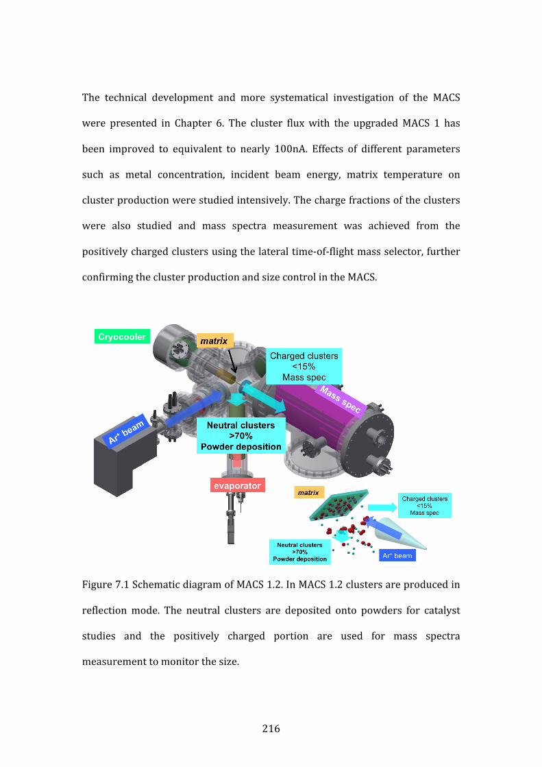
216
The technical development and more systematical investigation of the MACS
were presented in Chapter 6. The cluster flux with the upgraded MACS 1 has
been improved to equivalent to nearly 100nA. Effects of different parameters
such as metal concentration, incident beam energy, matrix temperature on
cluster production were studied intensively. The charge fractions of the clusters
were also studied and mass spectra measurement was achieved from the
positively charged clusters using the lateral time-‐of-‐flight mass selector, further
confirming the cluster production and size control in the MACS.
Figure 7.1 Schematic diagram of MACS 1.2. In MACS 1.2 clusters are produced in
reflection mode. The neutral clusters are deposited onto powders for catalyst
studies and the positively charged portion are used for mass spectra
measurement to monitor the size.

217
One of the biggest future challenges for the MACS is to understand the cluster
formation mechanism. Although we are able to produce clusters using the MACS
method, the mechanisms behind their formation still incompletely understood.
Simulation work is in progress (by Dr. L. Xu) to reveal what is happening in the
matrix during the Ar ions sputtering. The simulation results show that clusters
can be preformed in the matrix and the size of clusters remaining in the matrix
increases with the number of ions, which have bombarded the matrix. Other
challenges are technical issues in scaling up the production rate such as efficient
cooling, pre-‐cooling of the matrix gas, matrix replenishment, high flux ion beam
management and how to recycle metals which all require future investigations.
In short time, the next step of the MACS project is to upgrade the MACS 1 to
MACS 1.2. The schematic diagram of the MACS 1.2 is shown in Figure 7.1.
Clusters are produced in reflection mode in MACS 1.2. An ion source with 4mA
output current will be adopted. Based on the efficiency of 1%, by efficiency we
mean the number of clusters produced per argon ion incident on matrix from
which a cluster beam can be formed, we are aiming for 40μA cluster production
rate equivalent to ~10 milligram materials produced per hour. We have already
achieved over 10μA cluster production rate over 1 hour in recent experiments,
measured by QCM. According to the charge ratio results, the neutral clusters
(more than 70%) will be used to deposit onto a powder deposition system for
catalyst applications, where the positively charged clusters (less than 15%) will
be used to monitor the size of produced clusters in real time using the lateral
time-‐of-‐flight mass filter. The delivery time for MACS 1.2 will be this year. The
plan to build super abundant cluster source, the MACS 3, is also around the

218
corner. In MACS 3, an ion source (from microsystem) with beam current of
800mA will be applied. In principle, we are able to produce at least 1mA cluster
beam equivalent to grams of materials per hour using MACS 3, based on the
obtained efficiency. Other plans on the MACS are testing another matrix gas e.g.
using CO2 to replace Ar to save the cooling power and using laser instead Ar ions
to ablate the matrix.
Related Documents