1 Department of Information Engineering Capacitor • A capacitor is a device that stores charge – Capacitor is like reservoir that stores water – Capacitors differs in their capacity in storing charges conductor Insulator (vacuum, ceramic, plastic, metal oxide)

Department of Information Engineering104 Capacitor A capacitor is a device that stores charge –Capacitor is like reservoir that stores water –Capacitors.
Dec 19, 2015
Welcome message from author
This document is posted to help you gain knowledge. Please leave a comment to let me know what you think about it! Share it to your friends and learn new things together.
Transcript

1Department of Information Engineering
Capacitor
• A capacitor is a device that stores charge
– Capacitor is like reservoir that stores water
– Capacitors differs in their capacity in storing charges
conductor
Insulator (vacuum, ceramic,plastic, metal oxide)
2Department of Information Engineering
Charge up a capacitor
• Initially VC = 0, (0)
(0) CV V VI
R R
I
electrons
VC=0V
R
3Department of Information Engineering
• Because of the insulator in the capacitor, electrons moving into the –ve side are trapped
– the –ve side becomes –ve charged, +ve voltage side becomes +ve charged,
• VC across capacitor charge stored

4Department of Information Engineering
Capacitor
• Water analogy

5Department of Information Engineering
Definition of Capacitor
• Tub stores water, capacitor stores charge
– C = Tub size
– Q = Volume of water
– V = Height of water level
– I = Rate of flow of water
• If a capacitor contains Q amount of water (charges), and the height of water (V), then the size is given by
CQ
tub of sizewater of volume
V

6Department of Information Engineering
Capacitor
• C = size of the capacitor
Q Q
V or CC V
Large cap Small cap
Same charge (Q) but different V
V V

7Department of Information Engineering
Capacitors in parallel
• What is the combined capacitance C?
– Two tubs in parallel, can store more water, C should be larger
VC1
C2=
C?V

8Department of Information Engineering
Capacitor in parallel (C = C1+C2 )
• Parallel circuit, same voltage across C1 and C2
– Q1 = C1V, Q2 = C2V
– Total charge Q=Q1+Q2=(C1+C2)V
– C = = C1+ C2
C1
V
C2
V
Q
Same V for C1 and C2
VC1
C2
Q
V

9Department of Information Engineering
Capacitors in series
• What is the combined capacitance C?
VC1
C2
= C?V

10Department of Information Engineering
Capacitor in series
• Same current
– Therefore same amount of Q in both capacitors
C1
C2
V1
V2
V
I
Same QV depends on smaller cap
I
11Department of Information Engineering
Capacitor in series
• 1 2
1 2
1 21 2
1 2
1 2
1 2
,
V 1 1 1
Q
Q QV V
C C
Q QV V V
C C
C C C
C Chence C
C C

12Department of Information Engineering
• Resistor in series : R = R1 + R2
• Resistor in parallel :
• Capacitor in series :
• Capacitor in parallel : C = C1 + C2
1 2
1 1 1 R R R
1 2
1 1 1 C C C
13Department of Information Engineering
Capacitor
• Dump Q amount of water to a tub of size C, so that the water level is changed by V
• But
• Hence
– i.e. the rate of change of the height of water is proportional to the current (inflow of water)
CQ
V
Q I t
V dV I
t dt C

14Department of Information Engineering
Constant I
• Rate of increase of V = I/C,
• If I is constant, voltage increases constantly

15Department of Information Engineering
DC and AC circuits
• DC (direct current) circuits
– voltage is constant over time
– e.g. battery or lab power supply
• AC (alternate current) circuits
– voltage is varying over time
– Extremely important! Signal is represented as voltage variation
– e.g. your voice, modem signal, data signal

16Department of Information Engineering
DC circuit
• Initially VC = VC(0), find VC (t)
•
R
V0
VC
I
0 ( )( ) C CV V t dV
I t CR dt
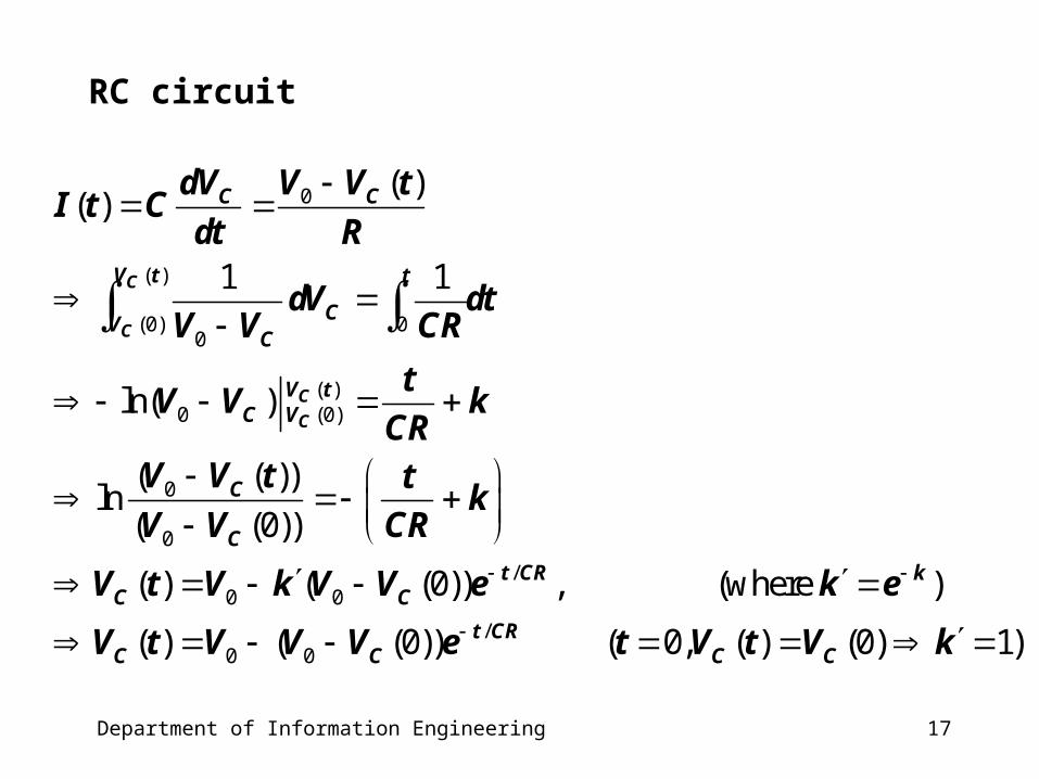
17Department of Information Engineering
RC circuit
0
( )
(0) 00
( )0 (0)
0
0
/0 0
/0 0
( )( )
1 1
ln( )
( ( ))ln
( (0))
( ) ( (0)) , (where )
( ) ( (0))
C
C
C
C
C C
V t t
CV
C
V tC V
C
C
t CR kC C
t CRC C
dV V V tI t C
dt R
dV dtV V CR
tV V k
CRV V t t
kV V CR
V t V k V V e k e
V t V V V e
( 0, ( ) (0) 1)C Ct V t V k
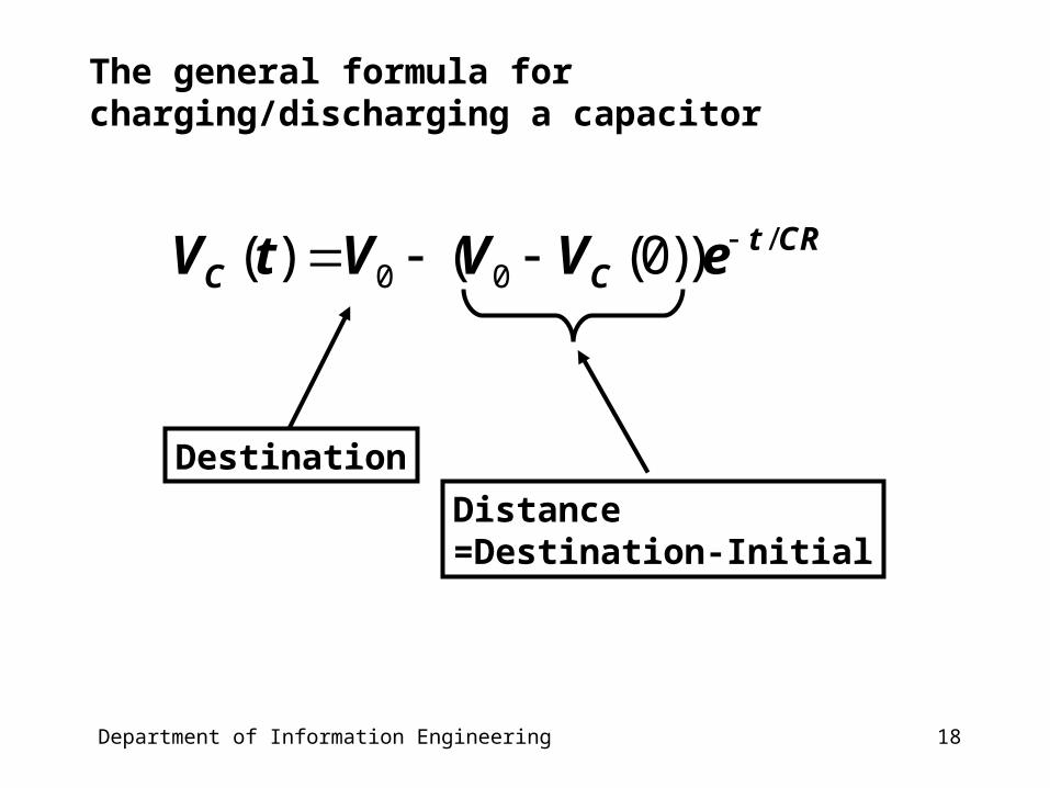
18Department of Information Engineering
The general formula for charging/discharging a capacitor
/0 0( ) ( (0)) t CR
C CV t V V V e
Destination
Distance=Destination-Initial

19Department of Information Engineering
Example - charging a capacitor
• At t=0, VC=0. What is VC(t)?
• Destination=V0
• Distance=V0-0=V0
• VC(t) = V0-V0e-t/RC = V0(1-e-t/RC)
R
V0
VC
I
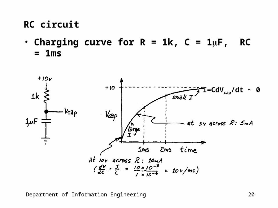
20Department of Information Engineering
RC circuit
• Charging curve for R = 1k, C = 1F, RC = 1ms
I=CdVcap/dt ~ 0

21Department of Information Engineering
How long does it take to charge up the capacitor?
• Depends on RC (the time constant)
• t=RC: VCAP(t) = 0.63 V0
• t=5RC: VCAP(t) = 0.99 V0
• t=5RC, the capacitor is almost fully charged up
– (to fully charge up a capacitor 100% takes infinitely long time, not practical)
• R = 1k, C = 1F, takes around 5ms to charge up

22Department of Information Engineering
Example
• Initially VC = 5V, V0=15V, find VC(t).
• Destination=15
• Distance=15-5=10
• Answer: VC(t) = 15 - 10e-t/RC
R
V0=15V
VC(0)=5V
I
23Department of Information Engineering
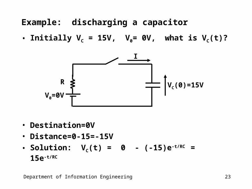
Example: discharging a capacitor
• Initially VC = 15V, V0= 0V, what is VC(t)?
• Destination=0V
• Distance=0-15=-15V
• Solution: VC(t) = 0 - (-15)e-t/RC = 15e-t/RC
R
V0=0V
VC(0)=15V
I
24Department of Information Engineering
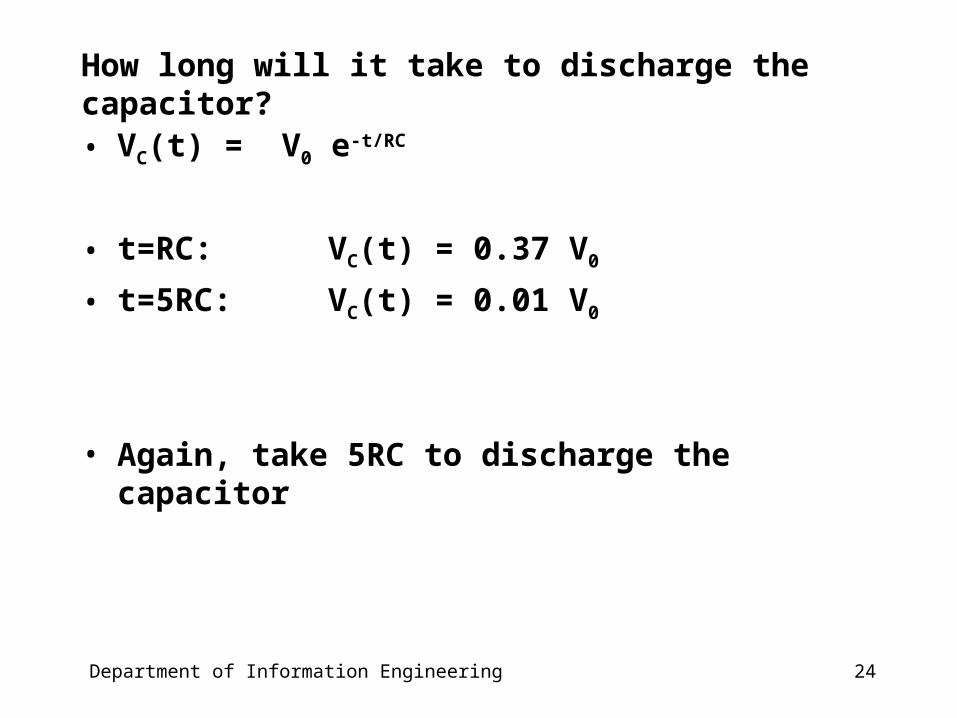
How long will it take to discharge the capacitor?
• VC(t) = V0 e-t/RC
• t=RC: VC(t) = 0.37 V0
• t=5RC: VC(t) = 0.01 V0
• Again, take 5RC to discharge the capacitor
25Department of Information Engineering
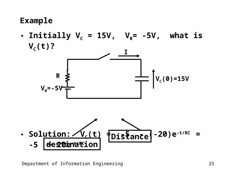
Example
• Initially VC = 15V, V0= -5V, what is VC(t)?
• Solution: VC(t) = -5 - (-20)e-t/RC = -5 + 20e-t/RC
R
V0=-5V
VC(0)=15V
I
destinationDistance

26Department of Information Engineering
AC circuit analysis
• If V1 is an AC voltage, what is V2?
R
C V2V1

27Department of Information Engineering
The importance of sinusoids
• In real world, interesting signals are time-varying
– if we pass the time-varying signal to a linear system, what is the output response?
Linear System(resistor,capacitor,and inductor)
?

28Department of Information Engineering
Sunglass example
• Sunglass is used to filter sun light
• Sun light is a varying signal, how to analyze it?
Sun light
29Department of Information Engineering
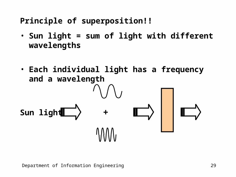
Principle of superposition!!
• Sun light = sum of light with different wavelengths
• Each individual light has a frequency and a wavelength
Sun light +

30Department of Information Engineering
Characteristic of a filter
• The filter (sunglass) can be characterized by its frequency response, that depends on only two parameters
– The attenuation factor (V2/V1)
– The phase (angle) change
V1 V2
31Department of Information Engineering
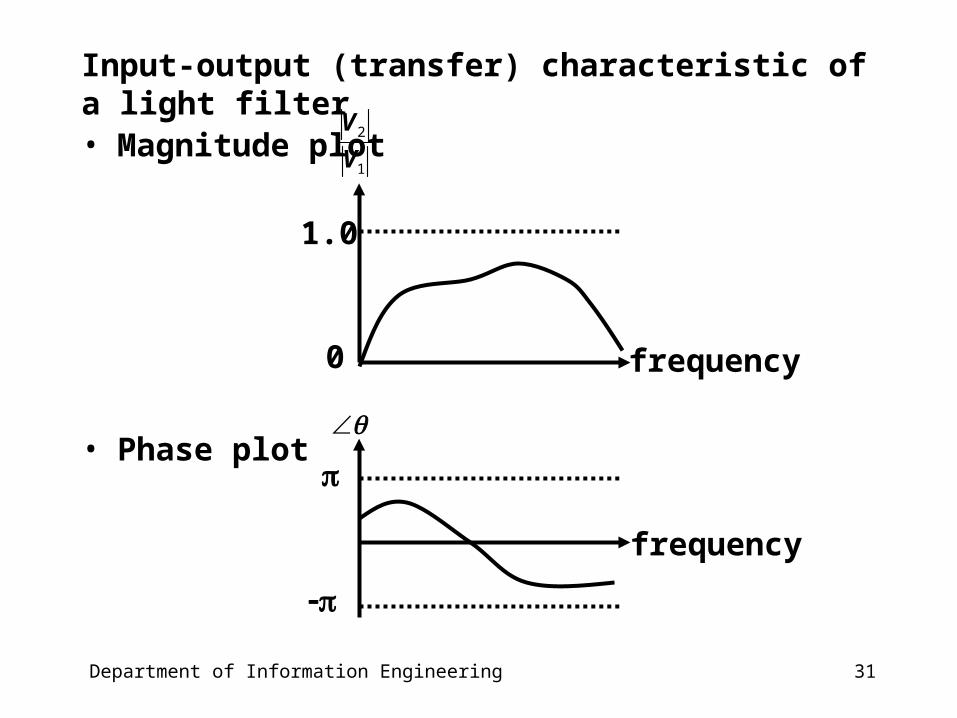
Input-output (transfer) characteristic of a light filter
• Magnitude plot
• Phase plot
2
1
V
V
frequency
frequency
1.0
0
32Department of Information Engineering
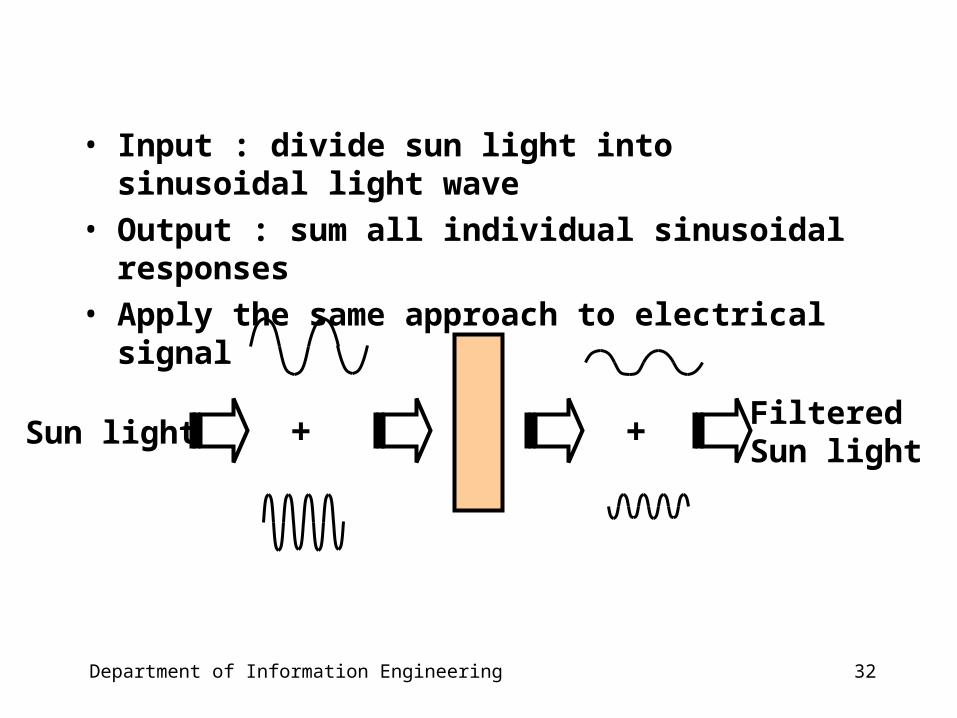
• Input : divide sun light into sinusoidal light wave
• Output : sum all individual sinusoidal responses
• Apply the same approach to electrical signal
Sun light + + FilteredSun light

33Department of Information Engineering
Fourier theorem: signal = sum of sinusoids
= sum of sinusoids
Linear Systemsinusoids
decompose
Sinusoidalresponses
sum
Output response
Input
Output = sum of sinusoids’ response
Input
34Department of Information Engineering
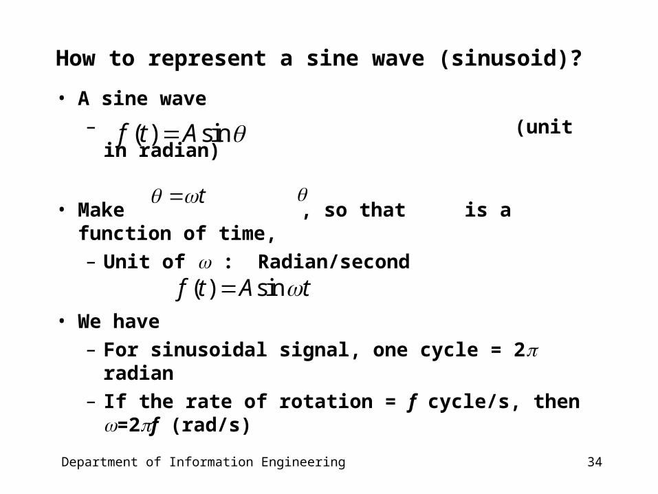
How to represent a sine wave (sinusoid)?
• A sine wave
– (unit in radian)
• Make , so that is a function of time,
– Unit of : Radian/second
• We have
– For sinusoidal signal, one cycle = 2 radian
– If the rate of rotation = f cycle/s, then =2f (rad/s)
( ) sinf t A
t
( ) sinf t A t

35Department of Information Engineering
Example : square wave = sum of sine waves !!
• Periodic square wave f(o) at frequency o
–
• 1kHz square wave = 1kHz + 3kHz +5kHz + . . . (sine waves)
0 0 0 0
4 1 1( ) (sin sin3 sin5 )
3 5w w w w f t t t
Fundamental freq Harmonics
36Department of Information Engineering
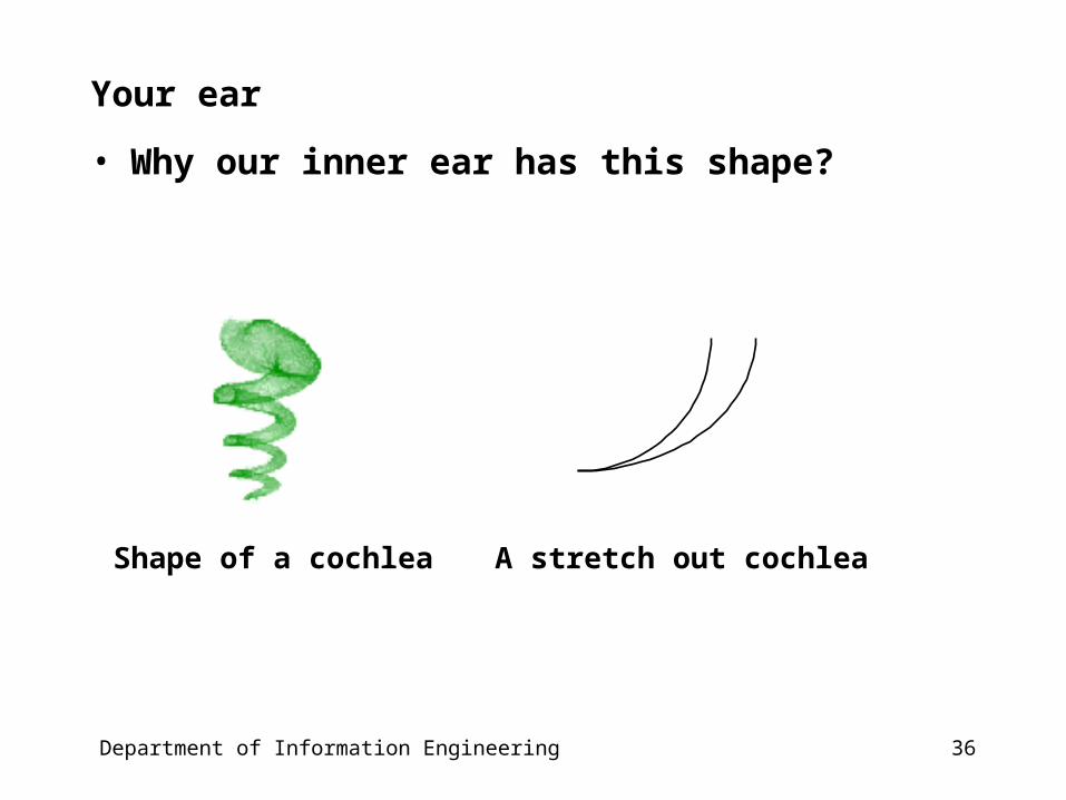
Your ear
• Why our inner ear has this shape?
Shape of a cochlea A stretch out cochlea

37Department of Information Engineering
Sinusoidal response of capacitor
• Let V = A cos wt (w = 2f)
• I = C dV/dt = - wC Asin wt
• Impedance = , complex relation because V and I are not in phase
~V
I
I leads V by 900
V
I
V
I

38Department of Information Engineering
j - complex number notation
• V and I are not in phase
– Apart from the ratio of magnitude between V and I
– Also need to know the phase angle between V and I
• To keep track with the magnitude and phase information
– sin and cosine are tedious to use
– Simpler to use a the j-notation

39Department of Information Engineering
A mathematician game
• The board
– 2 dimensional complex plane
– x-axis represents the real axis
• The player
– a vector (e.g. 1) on the plane
• The rule
– j represents an operation that rotates a vector anticlockwise by 90o on the complex plane
1 x
40Department of Information Engineering
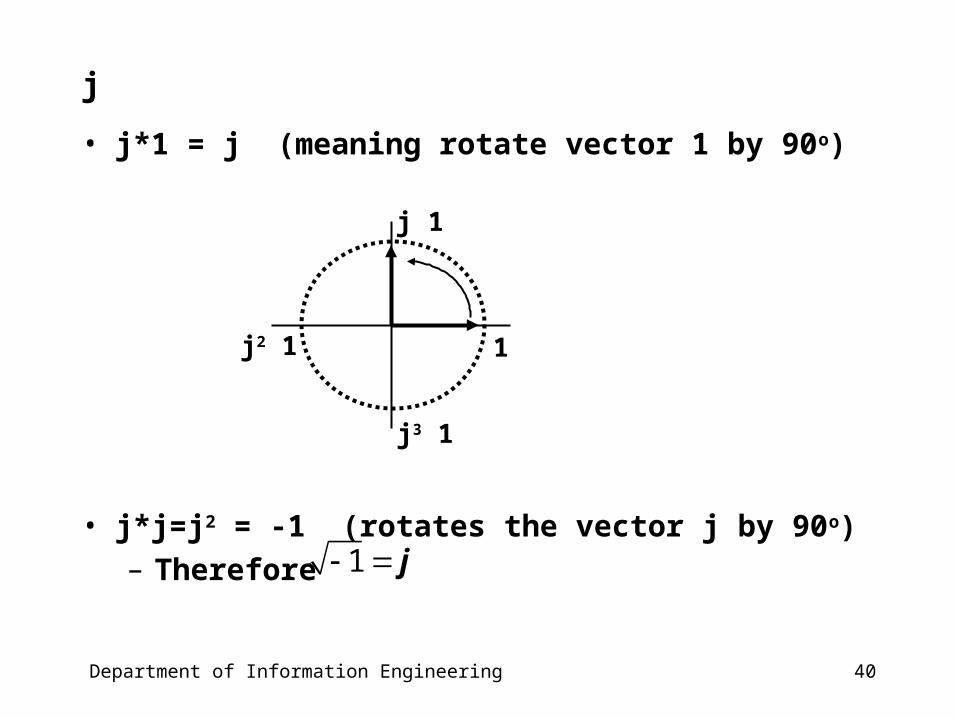
j
• j*1 = j (meaning rotate vector 1 by 90o)
• j*j=j2 = -1 (rotates the vector j by 90o)
– Therefore
1
j 1
j2 1
j3 1
1 j
41Department of Information Engineering
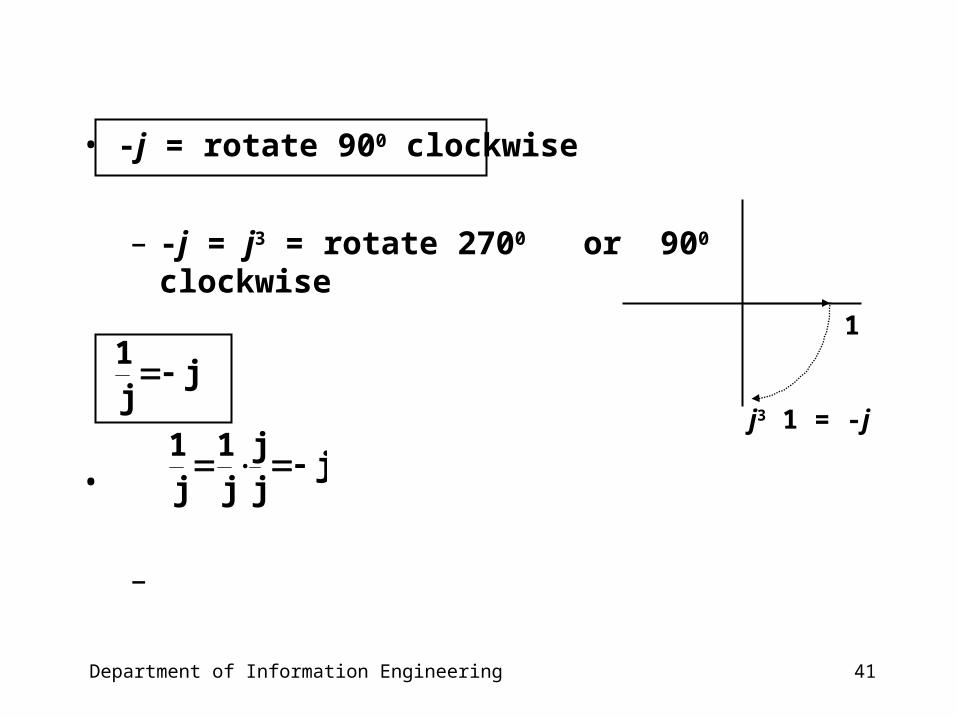
• -j = rotate 900 clockwise
– -j = j3 = rotate 2700 or 900 clockwise
•
–
1
j3 1 = -j
jjj
j1
j1
jj1

42Department of Information Engineering
j - complex number notation
• a+jb– Sum of vector a and jb– Represent a vector with a magnitude and phase
– Magnitude =
– Phase =
• – a vector with magnitude = 1 making angle with real axis
a
jb22 ba
ab
tan 1
cos sinj 1

43Department of Information Engineering
Euler formula
•
Euler formula
• Proof by series expansion of ex2 3
2 3
2 4 3 5
12! 3!
( ) ( )1
2! 3!
12! 4! 3! 5!
cos sin
x
j
x xe x
j je j
j
cos sin jj e
1
ej

44Department of Information Engineering
Complex sinusoid ejwt
•
– Represents a rotating vector that rotates at a rate of f cycles/sec ( )
j te
2 f
1
ejt
t
Direction of rotation
45Department of Information Engineering
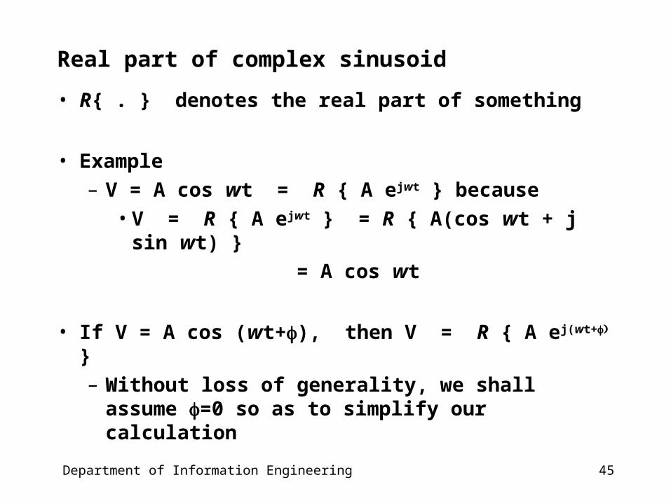
Real part of complex sinusoid
• R{ . } denotes the real part of something
• Example
– V = A cos wt = R { A ejwt } because
• V = R { A ejwt } = R { A(cos wt + j sin wt) }
= A cos wt
• If V = A cos (wt+), then V = R { A ej(wt+ }
– Without loss of generality, we shall assume =0 so as to simplify our calculation

46Department of Information Engineering
Impedance of a capacitor
•
• To recover V and I, take the real part
– V = R { A ejwt } = A cos wt
– I = R { jwC Aejwt } = R { jwC A (cos wt + j sin wt) }
= - wC A sin wt
1
j t
j t
C
V A e
dVI C j C Ae j C V
dtV
ZI j C
ω
ωω ω
ω(Ohm’s law for capacitor)
47Department of Information Engineering
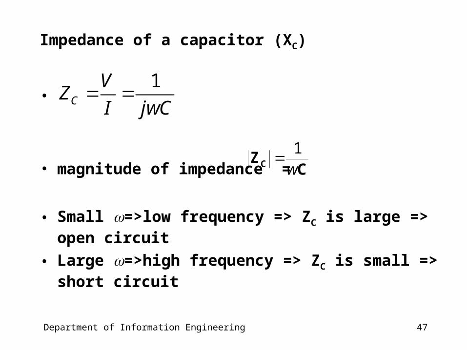
Impedance of a capacitor (XC)
•
• magnitude of impedance =
• Small =>low frequency => ZC is large => open circuit
• Large =>high frequency => ZC is small => short circuit
1 C
VZ
I jwC
1CZCw

48Department of Information Engineering
Circuit analysis
• If V2 is a varying signal, what is V2?
R
C V2V1
49Department of Information Engineering
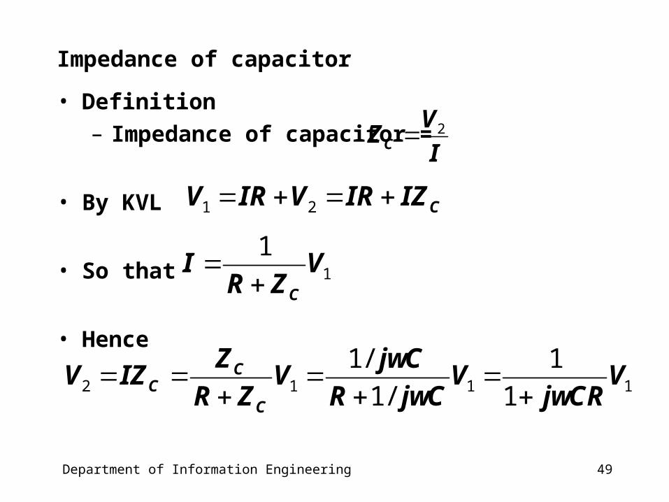
Impedance of capacitor
• Definition
– Impedance of capacitor =
• By KVL
• So that
• Hence
2C
VZ
I
1 2 CV IR V IR IZ
1
1
C
I VR Z
2 1 1 1
1/ 1
1/ 1C
CC
Z jwCV IZ V V V
R Z R jwC jwCR

50Department of Information Engineering
Transfer function T(w)
• Transfer function T(w)= Output / Input
=
• Note that the output response depends on the frequency of the input sinusoid
2
1
( ) 1
( ) 1
V w
V w jwCR

51Department of Information Engineering
Low pass filter
• Transfer function T(w)=
• High frequency ( ),
– High frequency signals are cut
• Low frequency ( ),
– Low frequency signals are passed
• The circuit is a low pass filter
2
1
( ) 1
( ) 1
V w
V w jwCR
w 2 ( ) 0V w
0w 2 ( ) 1V w

52Department of Information Engineering
A sketch of the frequency response of the circuit
VINVOUT
V1
C1
C2
R1
R2
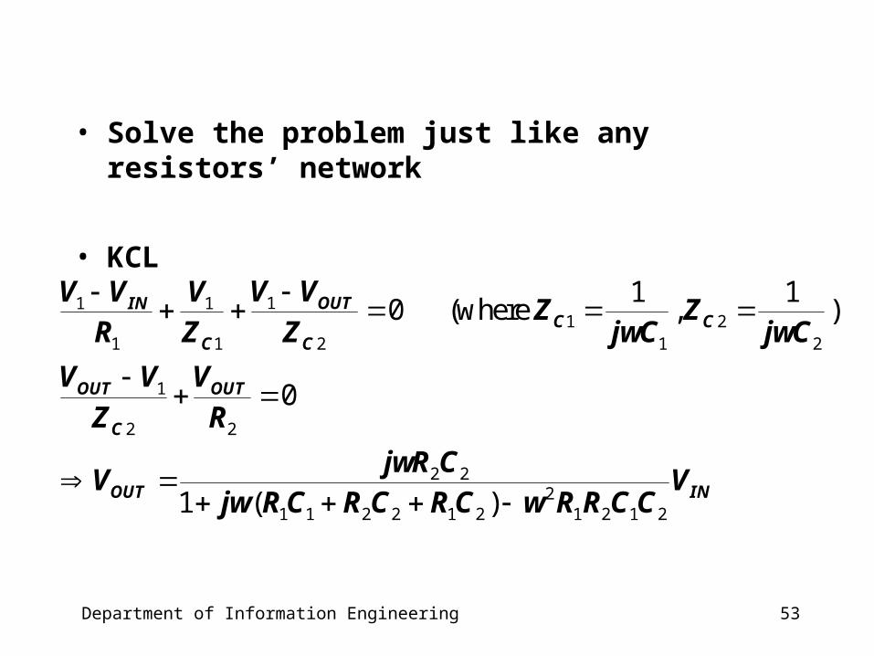
53Department of Information Engineering
• Solve the problem just like any resistors’ network
• KCL
11 11 2
1 1 2 1 2
1
2 2
2 22
1 1 2 2 1 2 1 2 1 2
1 10 (where , )
0
1 ( )
OUTINC C
C C
OUT OUT
C
OUT IN
V VV V VZ Z
R Z Z jwC jwC
V V V
Z R
jwR CV V
jw R C R C R C w R R C C
54Department of Information Engineering
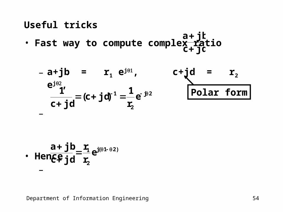
Useful tricks
• Fast way to compute complex ratio
– a+jb = r1 ej, c+jd = r2 ej,
–
• Hence
–
jdcjba
2j
2
1 er1
)jdc(jdc
1
)21(j
2
1 err
jdcjba
Polar form
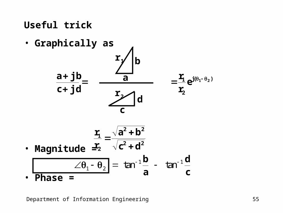
55Department of Information Engineering
Useful trick
• Graphically as
• Magnitude =
• Phase =
)(j
2
1 21err
jdcjba
a
br1
cd
r2
22
22
2
1
dc
barr
1 11 2 tan tan b d
a c

56Department of Information Engineering
Magnitude and phase response of a low pass filter (LPF)
•
– Magnitude response =
– Phase response =
jwCR11
VV
IN
OUT
2IN
OUT
)wCR(1
1V
V
)wCR(tanV
V 1
IN
OUT
57Department of Information Engineering
Important parameters of a filter
• What is the cut-off point of the filter?
• How steep is the cut-off slope?
– the steeper the better
58Department of Information Engineering
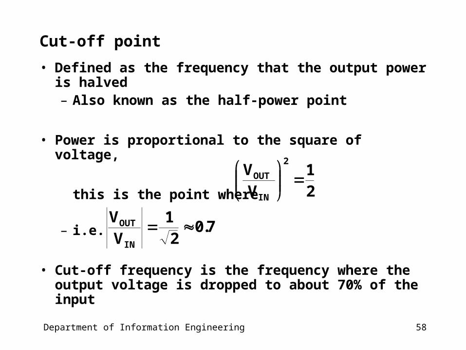
Cut-off point
• Defined as the frequency that the output power is halved– Also known as the half-power point
• Power is proportional to the square of voltage,
this is the point where
– i.e.
• Cut-off frequency is the frequency where the output voltage is dropped to about 70% of the input
21
V
V2
IN
OUT
7.02
1V
V
IN
OUT
59Department of Information Engineering
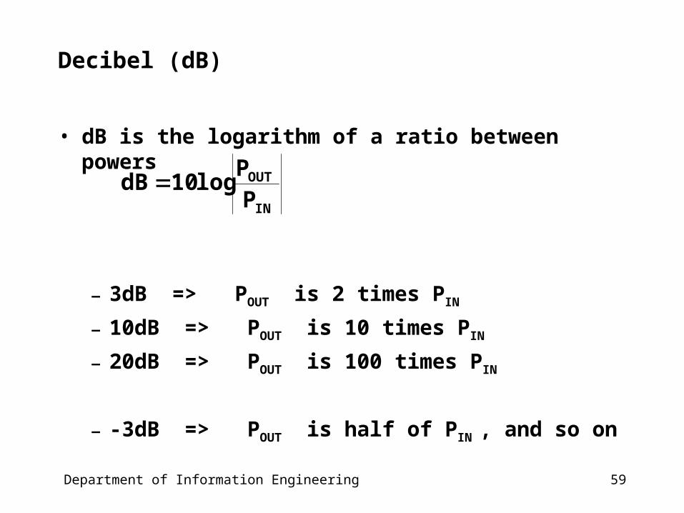
Decibel (dB)
• dB is the logarithm of a ratio between powers
– 3dB => POUT is 2 times PIN
– 10dB => POUT is 10 times PIN
– 20dB => POUT is 100 times PIN
– -3dB => POUT is half of PIN , and so on
IN
OUT
PP
log10dB
60Department of Information Engineering
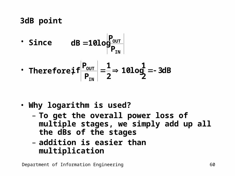
3dB point
• Since
• Therefore,
• Why logarithm is used?– To get the overall power loss of multiple stages, we
simply add up all the dBs of the stages– addition is easier than multiplication
IN
OUT
PP
log10dB
dB321
log1021
PP
ifIN
OUT

61Department of Information Engineering
• At half power point,
=> CCR = 1
=> C = 1/RC
• since C = 2f , therefore fC = 1/2RC
2
1 1 1
2 21 ( )OUT
IN
V
V wCR
3dB point of a LPF
Don’t forget the2 in exam!
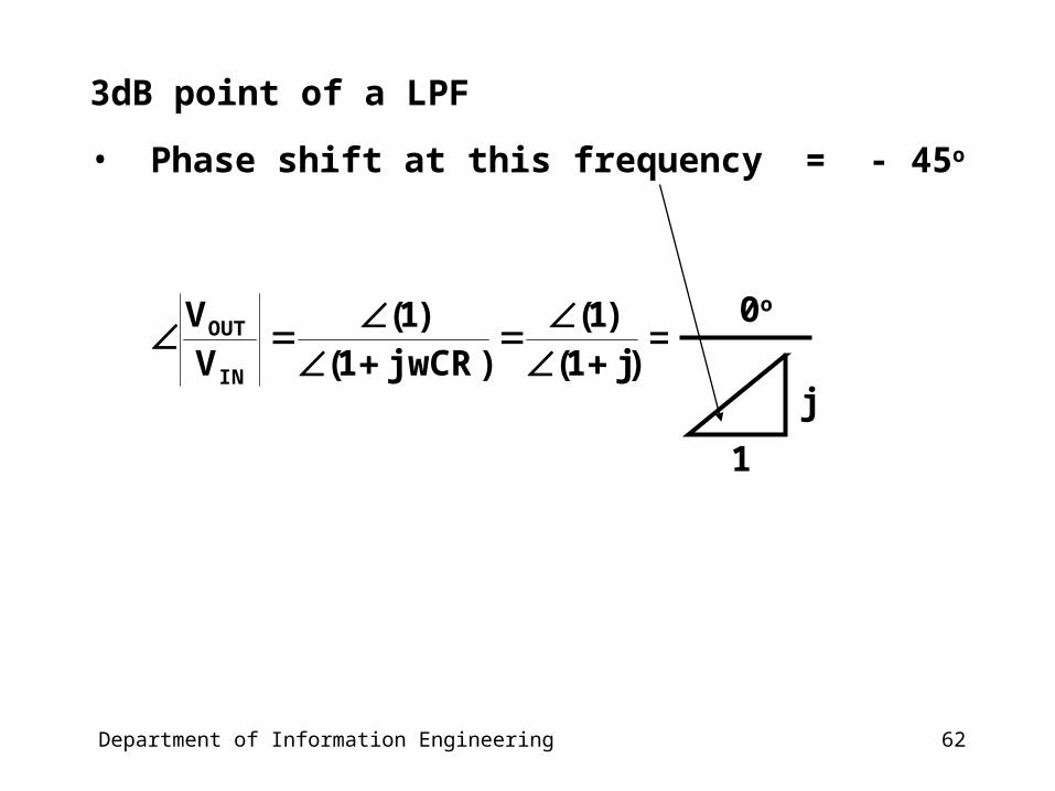
62Department of Information Engineering
• Phase shift at this frequency = - 45o
3dB point of a LPF
)j1()1(
)jwCR1()1(
VV
IN
OUT
j
0o
1

63Department of Information Engineering
Slope of the attenuation
• At 3dB point
– |jCR| = 1
• At frequency beyond the 3dB point
– |jCR| >> 1 , hence
• double the frequency , half the output voltage
1 1~
1
1
OUT
IN
OUT
IN
V
V j CR j CR
V
V CR

64Department of Information Engineering
• The slope falls at a rate of 6dB/octave
– in music, one octave = doubling of frequency
– Doubling the frequency , half the |VOUT/VIN|
=> POUT/PIN = 1/ 4 = -6dB
• Power is falling at a rate of 6dB per doubling of frequency
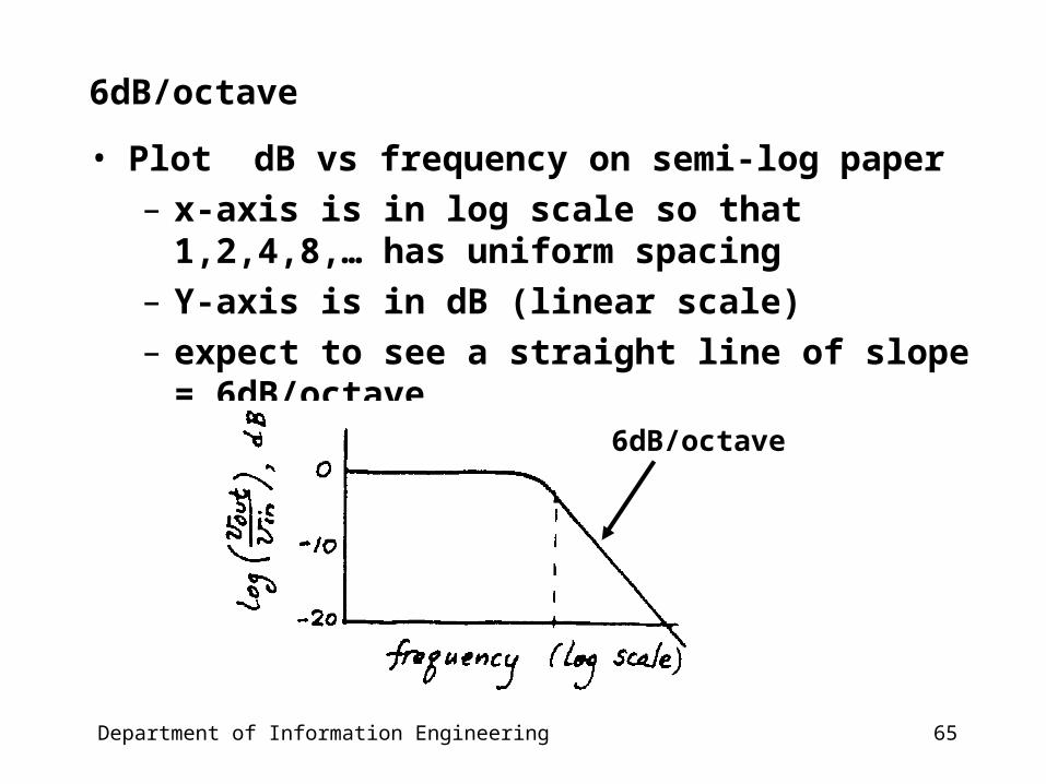
65Department of Information Engineering
6dB/octave
• Plot dB vs frequency on semi-log paper
– x-axis is in log scale so that 1,2,4,8,… has uniform spacing
– Y-axis is in dB (linear scale)
– expect to see a straight line of slope = 6dB/octave
6dB/octave

66Department of Information Engineering
High pass filter (HPF)
• At low freq
– cap is open circuit => VOUT ~ 0
• At high frequency
– cap is short circuit => VOUT ~ VIN
• Pass only high frequency
VinVout
VC

67Department of Information Engineering
High pass filter (HPF)
• 3dB point of HPF = 1/2RC
• Slope = 6dB/octave
90o
45o
0o
6dB/octave
68Department of Information Engineering
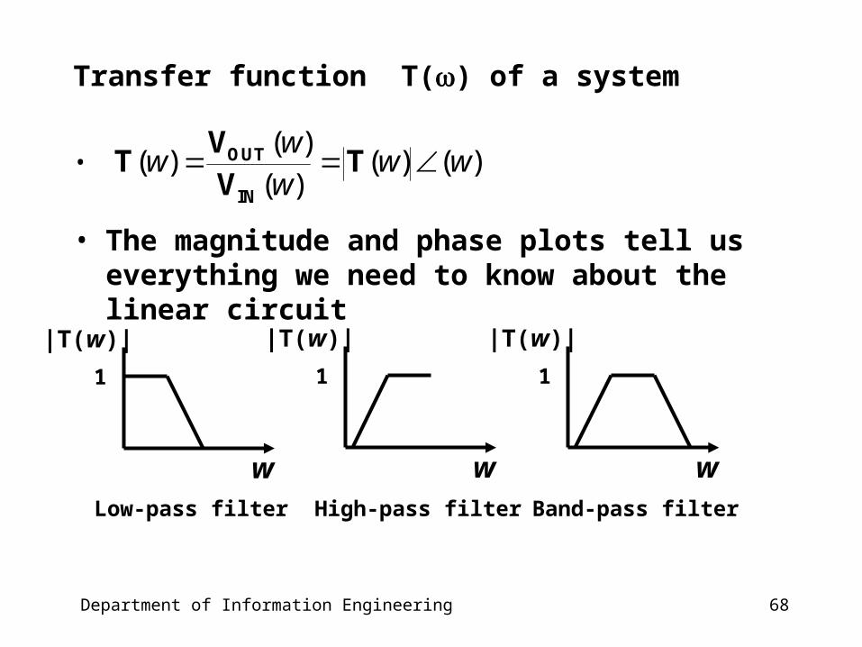
Transfer function T() of a system
•
• The magnitude and phase plots tell us everything we need to know about the linear circuit
( )( ) ( ) ( )
( )
ww w w
w OUT
IN
VT T
V
|T(w)|
w
1
Low-pass filter High-pass filter Band-pass filter
|T(w)|
w
1
|T(w)|
w
1
69Department of Information Engineering
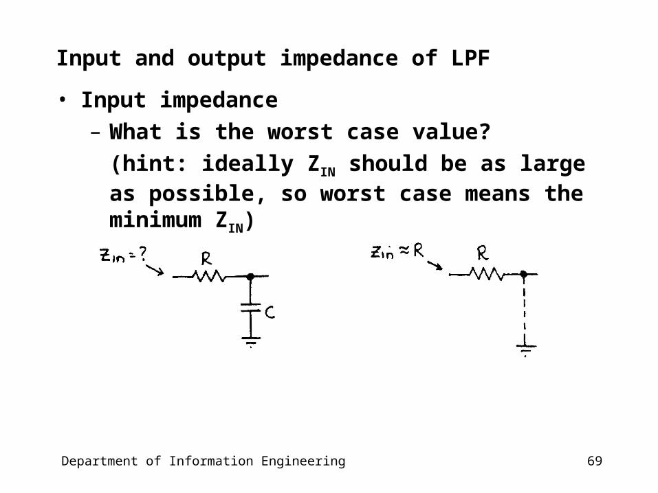
Input and output impedance of LPF
• Input impedance
– What is the worst case value?
(hint: ideally ZIN should be as large as possible, so worst case means the minimum ZIN)

70Department of Information Engineering
Input and output impedance of LPF
• Output impedance
– What is the worst case value?
(hint: ideally ZOUT should be as small as possible, so worst case means maximum ZOUT)

71Department of Information Engineering
Bandpass filter
• A filter that passes frequency only within the two 3dB points

72Department of Information Engineering
Bandpass filter
• Use a HPF to get rid of low frequency
f3db = 1/2RC~1600Hz

73Department of Information Engineering
Bandpass filter
• Use a LPF to get rid of high frequency
f3db = 1/2RC~8300Hz
74Department of Information Engineering
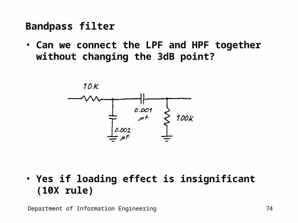
Bandpass filter
• Can we connect the LPF and HPF together without changing the 3dB point?
• Yes if loading effect is insignificant (10X rule)
75Department of Information Engineering
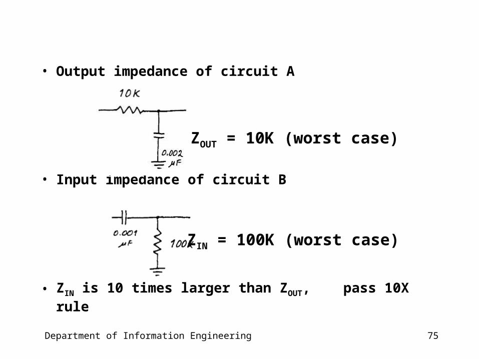
• Output impedance of circuit A
• Input impedance of circuit B
• ZIN is 10 times larger than ZOUT, pass 10X rule
ZOUT = 10K (worst case)
ZIN = 100K (worst case)
76Department of Information Engineering
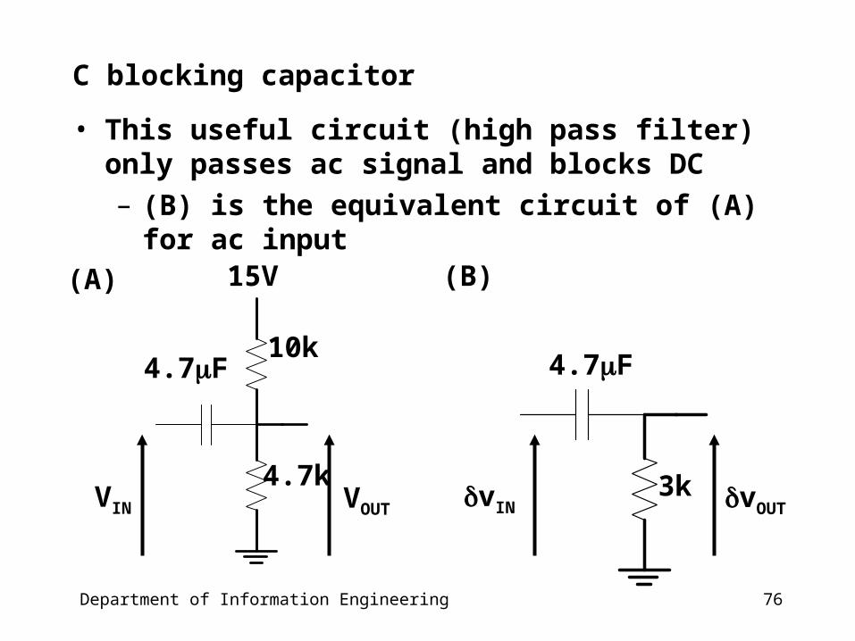
C blocking capacitor
• This useful circuit (high pass filter) only passes ac signal and blocks DC
– (B) is the equivalent circuit of (A) for ac input
VIN VOUT
4.7F
15V
10k
4.7kvIN
3k
4.7F
vOUT
(A) (B)

77Department of Information Engineering
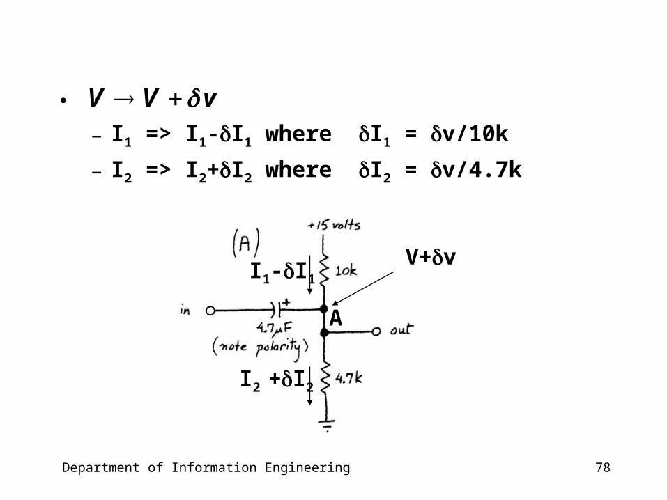
For ac signal, all DC voltage sources have zero impedance
• The 15V DC is like a zero impedance path to ground
– So the 4.7k and 10k are in parallel !!
• Why?
– Let the DC voltage at A be V, and the DC currents be I1 and I2
– If the ac signal at A is v, what is the ac current?
A
I1
I2
V V v
78Department of Information Engineering
•
– I1 => I1-I1 where I1 = v/10k
– I2 => I2+I2 where I2 = v/4.7k
A
V+vI1-I1
I2 +I2
V V v
79Department of Information Engineering
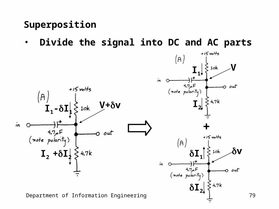
Superposition
• Divide the signal into DC and AC parts
V+vI1-I1
I2 +I2
VI1
I2
vI1
I2
+

80Department of Information Engineering
• Impedance sees by the ac signal =
•
• i.e. two resistors in parallel
v
I
1 2
10 * 4.7
10 4.7
v v k k
I I I k k
15V
II1
I2
To ac signal v,10k and 4.7k act as if in parallel

81Department of Information Engineering
DC blocking capacitor
• 3dB point?
–
– Pass signal with frequency > 11 Hz
6 3
1 1 1~ 11( )
2 2 *4.7*10 *3*10 f HzCR CR
vIN3k
4.7F
vOUT

82Department of Information Engineering
The design of a good probe
• Good probe has a very large input impedance
• but be careful with the cable’s capacitance !!
cable Large impedancee.g. 1M
probe

83Department of Information Engineering
Design of a coaxial cable (also known as BNC cable)
signal
ground
Ground clip
probe
shield
0VVin
Tiny capacitance(between signal and ground)

84Department of Information Engineering
• coaxial cable (coax)– high quality cable, able to carry very high
frequency, used in cable TV (video frequency is very high), and in laboratories
• The shield acts as a Faraday cage
• e.g. like your microwave oven
– external interference (energy) cannot penetrate into the wire (less noise), and signal energy inside cannot leak out

85Department of Information Engineering
Effect of the tiny stray capacitance
• Cable capacitance is in parallel with input impedance
• Typical value of cable capacitance?– 30pF/foot – 4 feet cable ~ 120pF (pF = 10-12F)
• Impedance of ZC
– At 1kHz, |ZC|=1.3M– At 1MHz, |ZC|~1.3k
• Problem– Scope’s input impedance is reduced at high frequency !
1M
86Department of Information Engineering
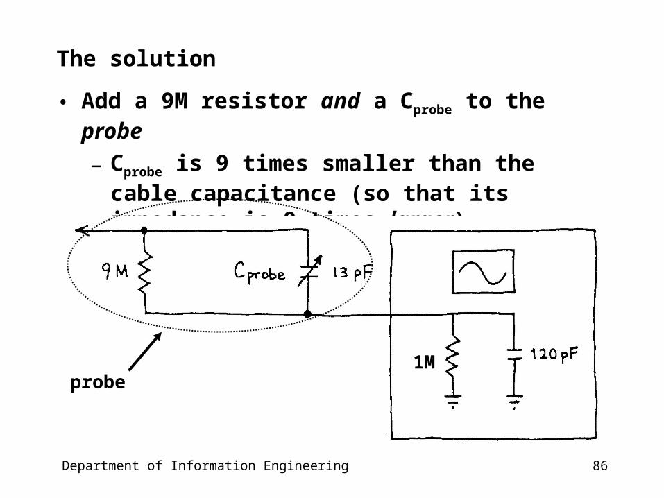
The solution
• Add a 9M resistor and a Cprobe to the probe
– Cprobe is 9 times smaller than the cable capacitance (so that its impedance is 9 times larger)
probe1M

87Department of Information Engineering
•
=
9X=
X=jwCR1R
jwCR1R9
19 10
OUT
IN
V XV X X
88Department of Information Engineering
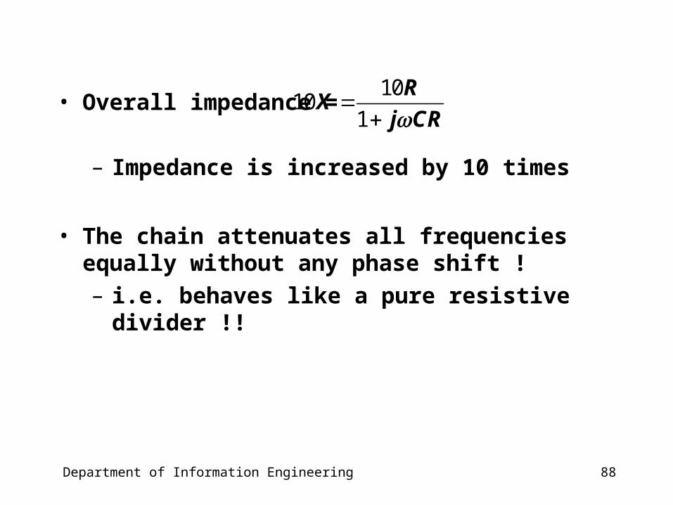
• Overall impedance =
– Impedance is increased by 10 times
• The chain attenuates all frequencies equally without any phase shift !
– i.e. behaves like a pure resistive divider !!
1010
1
RX
j CR
89Department of Information Engineering
10X input
• Always use 10X mode provides by the probe
– Why? Because input impedance is increased
• But remember the displayed signal is ten times smaller (because of 10:1 attenuation), so you need to multiply the signal by 10
• Probe compensation
– Our method only works if Cprobe is exactly nine times smaller than Cstray
– How to make this adjustment ?
90Department of Information Engineering
How to adjust the probe?
• square wave = sum of infinitely number of sinusoids
• feeding a square wave signal to the scope is like feeding a full range of sinusoids simultaneously
• square wave is easy to generate
– the scope has a square wave output (1kHz)

91Department of Information Engineering
How to adjust the probe?
• Use the x10 probe to see the square wave
– if the value of Cprobe is correct, then all the sinusoids are reduced exactly by 10 times smaller
– see a perfect square wave that is 10 times smaller
• If the value of Cprobe is not right, then some frequencies will be attenuated more than the other; the square wave would not be perfect
• Adjust Cprobe so that a perfect square wave can be seen

92Department of Information Engineering
Using square wave to tune the probe
(to get this perfect square wave,the probe must pass all frequencies uniformly)

93Department of Information Engineering
Inductor
• Ampere‘s Law
– current generates magnetic field
– direction of magnetic flux : right-hand screw law
currentMagnetic flux
Current flowsinto paper

94Department of Information Engineering
Inductor
• Straight wire generates a weak magnetic field
• Core generates a stronger field
– The magnetic field is aligned in the same direction
– Weak forces add up to a stronger force
current
95Department of Information Engineering
Inductor
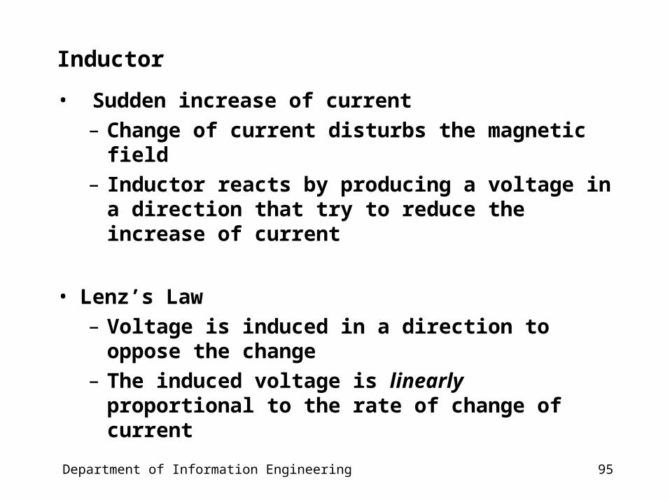
• Sudden increase of current
– Change of current disturbs the magnetic field
– Inductor reacts by producing a voltage in a direction that try to reduce the increase of current
• Lenz’s Law
– Voltage is induced in a direction to oppose the change
– The induced voltage is linearly proportional to the rate of change of current
96Department of Information Engineering
Inductor
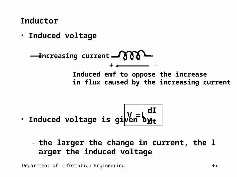
• Induced voltage
• Induced voltage is given by
– the larger the change in current, the larger the induced voltage
Increasing current
Induced emf to oppose the increase in flux caused by the increasing current
dIV L
dt
+ -

97Department of Information Engineering
Inductor
• Example
– Switch closed at t=0, what is I?
– At t<0, I=0 (because of open circuit)
V
L
R
I

98Department of Information Engineering
Inductor
• After the switch is closed, I goes up, so voltage VL is induced in a direction to oppose the flow of I
V
L
R
I
VL

99Department of Information Engineering
• KVL gives
• Initial condition, I(0)=0, therefore k=1
• Hence
0 0
( )
0 00
0 0
(where )
1
( )
RL
I t t
t
dIV L IR
dtL dI V
I I IR dt R
RdI dt
I I L
I t I kI e
0 0( )
RL
tI t I I e

100Department of Information Engineering
Inductor
• An application – choke
– lightning can cause a sudden surge of current, which may damage your equipments
– an inductor can be used to smooth the surge
• Time constant = R/L
• After 5 , the change of I is negligible, , the inductor is like a short circuit
I
t
I0
0L
dIV L
dt

101Department of Information Engineering
Impedance of inductor
•
• impedance ZL =
• Note
– voltage leads current by 90o
– at low frequency (small ), inductor ~ short-circuit
– at high frequency (large ), inductor ~ open-circuit
w
ww
j t
j t
I Ae
dIV L j LAe
dt
wVj L
I
102Department of Information Engineering
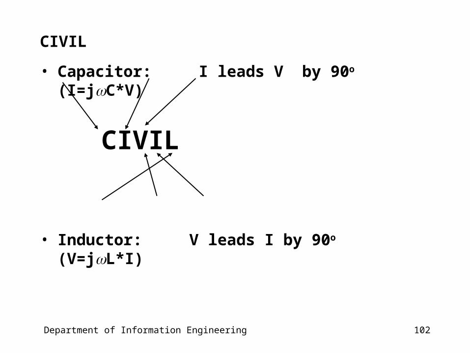
CIVIL
• Capacitor: I leads V by 90o (I=jC*V)
• Inductor: V leads I by 90o (V=jL*I)
CIVIL

103Department of Information Engineering
LC circuit
• Quick analysis
– at low freq, C is open circuit
• VOUT = VIN
– at high freq, L is open circuit
• VOUT = VIN
– a notch filter !
VOUT/VIN
freq
1

104Department of Information Engineering
LC circuit
• By calculation
•
2
2
11
OUT C L
IN C L
V X X w LCV R X X jwCR w LC
2
0, 1
1, 0
, 1
OUT
IN
OUT
IN
OUT
IN
Vw
V
Vw
LC V
Vw
V

105Department of Information Engineering
Another LC resonant circuit (lab work)
• Frequency response?
• at low frequency
– L is short circuit, C is open circuit, VOUT = 0
• at high frequency
– L is open circuit, C is short circuit, VOUT = 0

106Department of Information Engineering
LC resonant circuit
• The resonant circuit is highly selective
– only pass a narrow range of frequencies
– Usage: tuner circuit in radio receiver
• Q-factor
– a measure of the narrowness of the peak
– the narrower, the better
– Q = f0/f3dB
• (f3dB is the width of the two 3dB points)
• (f0 is the peak frequency)

107Department of Information Engineering
To verify the Fourier components of a square wave
• In the lab, centered the tune circuit at 16kHz
• Drive the circuit with a square wave ranging from 0Hz to 16kHz, at what frequencies would the tune circuit detect large outputs?
–
– 16kHz (fundamental freq of 16kHz)
– 16/3 kHz (2nd harmonic of 16/3kHz = 16kHz)
– 16/5 kHz (3rd harmonic of 16/5 kHz = 16kHz)
0 0 0 0
4 1 1( ) (sin sin3 sin5 )
3 5w w w w f t t t

108Department of Information Engineering
Transmission line
• Medium that transmits signal/energy from one place to another is called an transmission line
– e.g. coaxial cable, telephone wires, optical fibre, wave guides, power lines

109Department of Information Engineering
A cable of length L
• Why the impedance of coaxial cable is 50/75 ?
• What is the propagation speed of the voltage signal?
• How long does it take for the signal to reach RLoad?
• What is the voltage and current along the cable?
• Why some time you hear echo in phone call?
• How to eliminate the echo?
VS
RS
RLoadV(z,t)
I(z,t)
z
L
110Department of Information Engineering
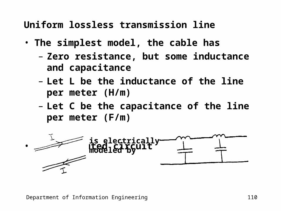
Uniform lossless transmission line
• The simplest model, the cable has
– Zero resistance, but some inductance and capacitance
– Let L be the inductance of the line per meter (H/m)
– Let C be the capacitance of the line per meter (F/m)
• A distributed circuit
is electricallymodeled by
111Department of Information Engineering
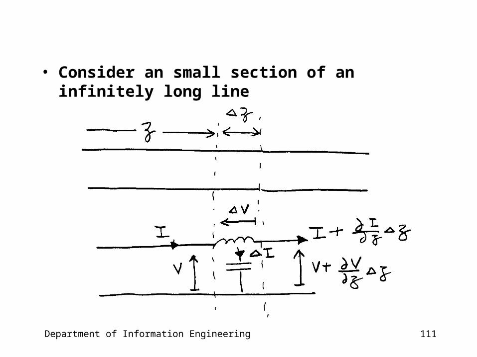
• Consider an small section of an infinitely long line
112Department of Information Engineering
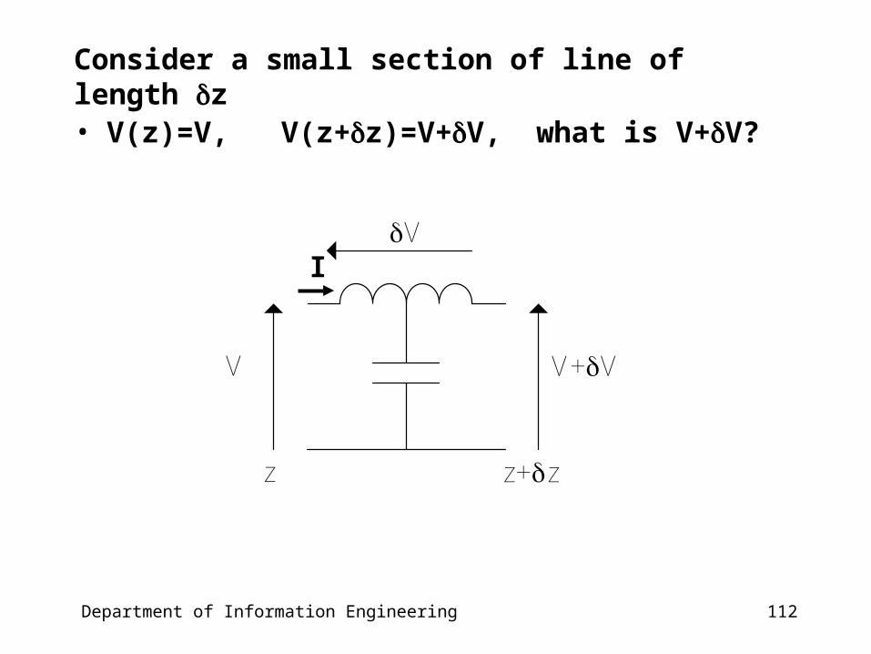
Consider a small section of line of length z
• V(z)=V, V(z+z)=V+V, what is V+V?
V V+V
V
z z+z
I

113Department of Information Engineering
Consider a small section of line of length z
• What is V?
–
V V+V
V
z z+z
I
IV L z
t

114Department of Information Engineering
Consider a small section of line of length z
• ( )V zV V V z
z
z z+z
V(z)
( )V z
z
V V
V
z

115Department of Information Engineering
(1)
V V V V
I VL z V z
t z
V IL
z t
Apply KVL to the section
V V+V
V
z z+z
116Department of Information Engineering
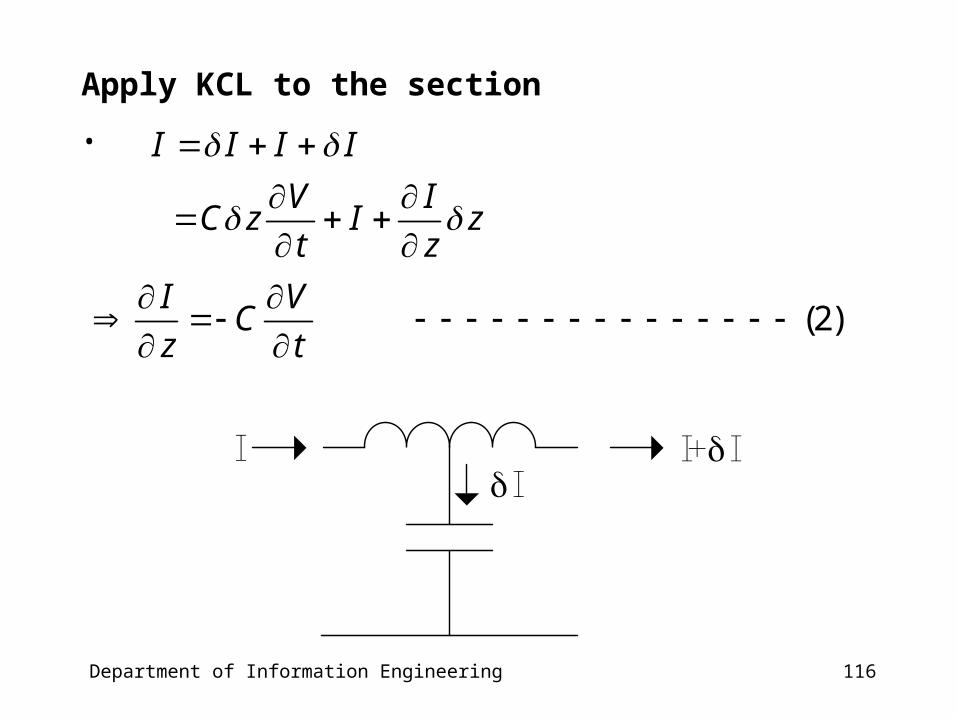
Apply KCL to the section
•
(2)
I I I I
V IC z I z
t z
I VC
z t
I I+II

117Department of Information Engineering
• Fundamental equations for the line
• To solve, differentiate (1) with respect to z
• differentiate (2) with respect to t
)2(tV
CzI
,)1(tI
LzV
tzI
LzV 2
2
2
2
22
tV
Ctz
I

118Department of Information Engineering
• Hence
• recast the voltage wave equation into the form
• where is the characteristic velocity of the line
)equationwavecurrent(tI
LCzI
)equationwavevoltage(tV
LCzV
2
2
2
2
2
2
2
2
2
2
22
2
tV
u1
zV
LC1
u

119Department of Information Engineering
• What does the equation mean?
• If our derivation is correct, then the voltage signal V(z,t) must satisfy the voltage wave equation
• So what are the solutions to this voltage wave equation?
– Any functions that have the form V=f(z-ut) are solutions, where f(.) is an arbitray function
– e.g. cos(z-ut), (z-ut)3.5, e-(z-ut), …
2
2
22
2
tV
u1
zV
120Department of Information Engineering
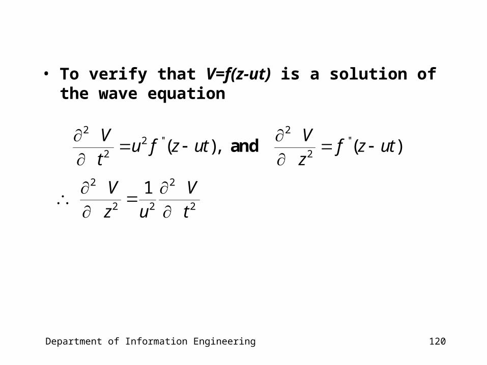
• To verify that V=f(z-ut) is a solution of the wave equation
2 22 '' ''
2 2
2 2
2 2 2
( ), ( )
1
V Vu f z ut f z ut
t z
V Vz u t
and

121Department of Information Engineering
f(z-ut)
• f(z) is a stationary function
– e.g. cos(z)
• f(z-ut) shift the function by ut in the +ve z direction
– e.g. cos(z-ut)
• f(z-ut) describes a traveling wave moving in the +z direction
• Similarly, g(z+ut) describes a traveling wave in the –z dir
ut
122Department of Information Engineering
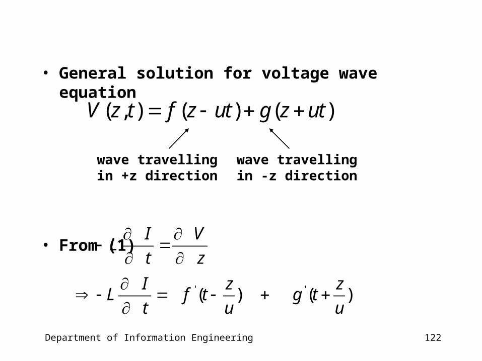
• General solution for voltage wave equation
• From (1)
( , ) ( ) ( )V z t f z ut g z ut
wave travellingin +z direction
wave travellingin -z direction
' '
( ) ( )
I VL
t z
I z zL f t g t
t u u
123Department of Information Engineering
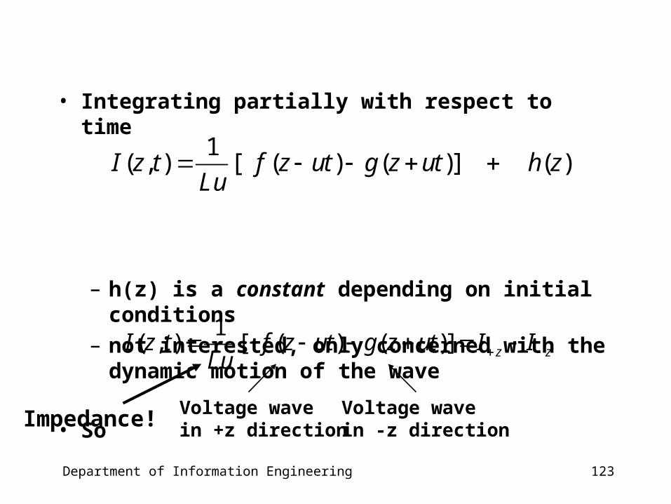
• Integrating partially with respect to time
– h(z) is a constant depending on initial conditions
– not interested, only concerned with the dynamic motion of the wave
• So
1( , ) [ ( ) ( )] ( )I z t f z ut g z ut h z
Lu
1( , ) [ ( ) ( )] z zI z t f z ut g z ut I I
Lu
Voltage wave in +z direction
Voltage wavein -z directionImpedance!

124Department of Information Engineering
• Overall voltage = f(z-ut) + g(z+ut)
V=f(z-ut)
+z direction
V=g(z-ut)
( , ) ( ) ( )V z t f z ut g z ut
Resultant voltage= f(z-ut)+g(z+ut)

125Department of Information Engineering
0
1( , ) [ ( ) ( )] z zI z t f z ut g z ut I I
Z •
• Overall current I = I+z – I-z
0
( )z
f z utI
Z
V=f(z-ut)
+z direction
V=g(z-ut)
0
( )z
g z utI
Z
z zI I I

126Department of Information Engineering
• characteristic impedance of the line
• so this is the impedance looking into an infinitely long line !!
• signal propagation velocity
CL
LuZ0
LC1
u

127Department of Information Engineering
Example - Category 5 cable
• Category 5 cable is high-grade telephone cable
– commonly used for connecting Ethernet
• Data sheet
– impedance: 100 ohms +/- 15%, 1MHz to 200 MHz
– capacitance: 5.6nF /100 m max
– DC resistance: 9.38 ohms/100 m max
– Propagation delay: 538 ns/100 m @ 100 MHz

128Department of Information Engineering
Example - Cat 5 cable
• What is L?
• Does it agree with the propagation velocity in the spec?
• Speed quoted in the spec =
m100/H5610CL
)caseourin(100CL
Z
4
0
s/m108.1
1056
1
1056106.5
1LC1
u
8
202118
s/m1085.1s/m10538
100 89

129Department of Information Engineering
An old problem (?) revisited
• What is V?
• Initially, the source see the source impedance in series with Z0 !!
– voltage (Vi) transmitted into the cable is given by
0
iiS
0S
0i Z
VI ,V
ZR
ZVV

130Department of Information Engineering
• So V will be the voltage we see -- if we have an infinitely long cable
• But the length of our cable is finite, the traveling voltage wave will reach the end of cable typically at a speed of 2/3 of speed of light (2 x 10⁸ m/sec)
• Suppose the cable is terminated by a load RL, and if
then we have a discontinuity at the boundary,RIV
Li
i

131Department of Information Engineering
• Reflection and transmission at the boundary
• incident voltage and current relation:
• boundary condition:
0i
i ZIV
LRIV
V

132Department of Information Engineering
• To satisfy the boundary condition, a portion of voltage and current waves must be reflected
– Vr and Ir are the reflected waves
• And the incident and reflected waves both satisfy
–
such that i r i rL
i r i r
V V V V VVR
I I I I I I
0i r
i r
V VZ
I I

133Department of Information Engineering
Reflection coefficient
• Let be the reflecting coefficient
• Since
• rearranging the above equation, we have
0 0
0 0
, ,
11
i r i rL i r
i r
i rL
i r
V V V VVR but I I
I I I Z Z
V VR Z Z
V V
i
r
VV
0
0
Lr
i L
R ZV
V R Z

134Department of Information Engineering
Matched termination RL = Z0
• Important special case
– If RL = Z0, then =0
– No reflection (good!)
– This situation is called matched termination
• In communication, reflection is not good (this is why you can hear echo)
• Always match the line by making RL = Z0 if possible

135Department of Information Engineering
Transmission coefficient
• How much voltage is transmitted to the load?
– Hence
• If the line is matched (RL=Z0), then maximum energy is transmitted to the load (=0, =1)
1V
VVVV
i
ri
i
0L
L
ZRR2
136Department of Information Engineering
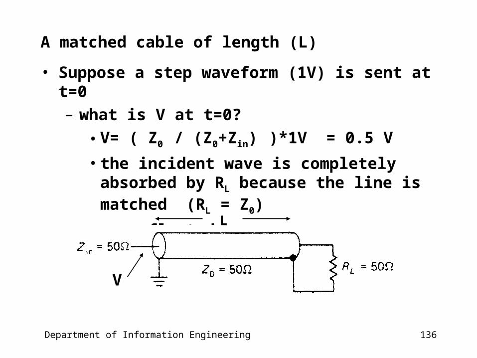
A matched cable of length (L)
• Suppose a step waveform (1V) is sent at t=0
– what is V at t=0?
• V= ( Z0 / (Z0+Zin) )*1V = 0.5 V
• the incident wave is completely absorbed by RL because the line is matched (RL = Z0)
• no reflected wave
V
L

137Department of Information Engineering
A shorted cable of length (L)
• What if RL =0 (short circuit)?
– You know the answer, V=0, but NOT at the beginning!
• At t=0
– V= ( Z0 / (Z0+Zin) )*1V = 0.5 V
138Department of Information Engineering
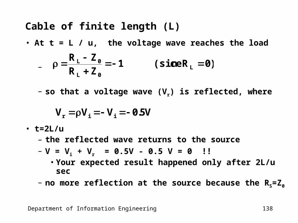
Cable of finite length (L)
• At t = L / u, the voltage wave reaches the load
–
– so that a voltage wave (Vr) is reflected, where
• t=2L/u– the reflected wave returns to the source– V = Vi + Vr = 0.5V - 0.5 V = 0 !!
• Your expected result happened only after 2L/u sec– no more reflection at the source because the RS=Z0
)0Rce(sin1ZR
ZRL
0L
0L
V5.0VVV iir
139Department of Information Engineering
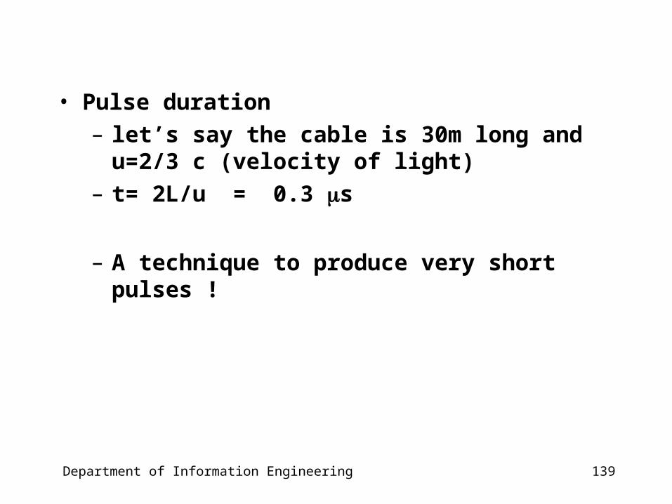
• Pulse duration
– let’s say the cable is 30m long and u=2/3 c (velocity of light)
– t= 2L/u = 0.3 s
– A technique to produce very short pulses !

140Department of Information Engineering
General case
• The case where the source, the line and the load impedances are all different
– reflection coefficient at the load = L
– reflection coefficient at the source = S
0L
0L
ZR
ZR
0S
0S
ZR
ZR

141Department of Information Engineering
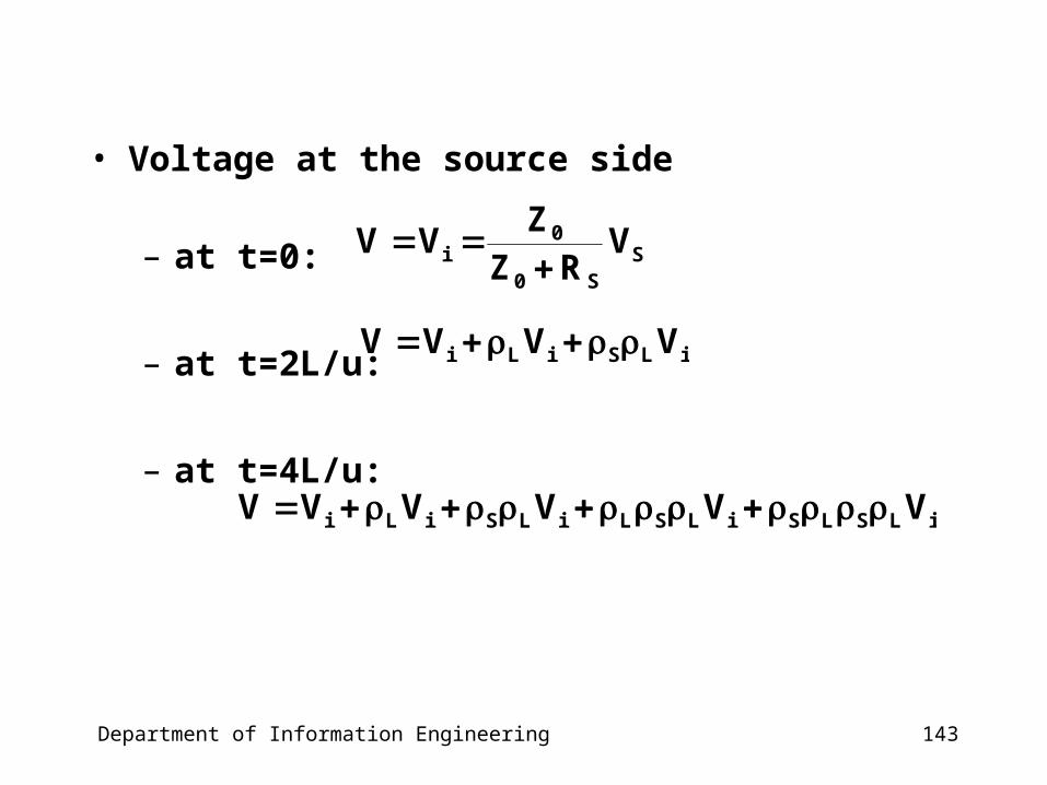
• Voltage at the source side
– at t=0: SS0
0i V
RZ
ZVV
VS
RS
RLoad
L
ViV

142Department of Information Engineering
• Voltage at the source side
– at t=2L/u: iLSiLi VVVV
VS
RS
RLoad
L
ViV pLVi
pSpLVi
143Department of Information Engineering
• Voltage at the source side
– at t=0:
– at t=2L/u:
– at t=4L/u:
SS0
0i V
RZ
ZVV
iLSiLi VVVV
iLSLSiLSLiLSiLi VVVVVV

144Department of Information Engineering
• Add everything up
–
• since
• therefore
))1()(1(V
)1(V
)1(VV
LSL2
LSLSi
LSLLLSLSLSi
LSLSLSLLSLi
1|x|forxx1x1
1 2
11 1
1 1 1
(the line impedance disappeared !!)
Li L i
S L S L S L
LS
S L
V V V
RV
R R
145Department of Information Engineering
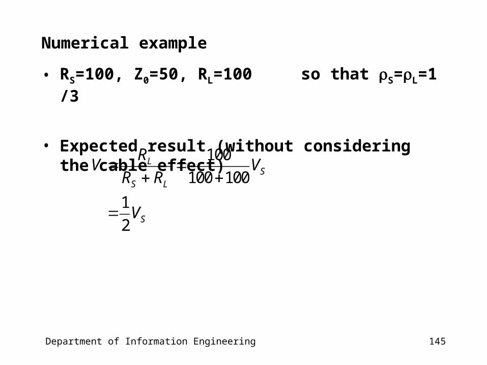
Numerical example
• RS=100, Z0=50, RL=100 so that S=L=1/3
• Expected result (without considering the cable effect)
100
100 100
1
2
LS
S L
S
RV V
R R
V

146Department of Information Engineering
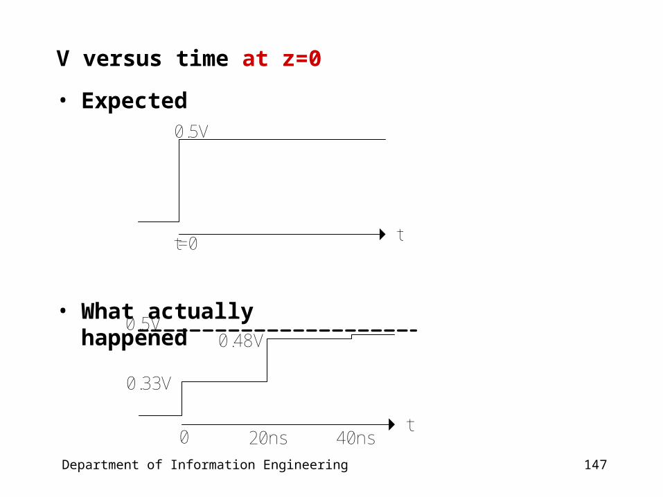
A sketch of the waveform of V versus time
• e.g. cable length=1m, u=2*108 m/s
– t=0, V=(50/150)VS = 0.33 VS
– t=2L/u=20ns, V = 1/3 VS ( 1 + L + L S )
= 1/3 VS (1 + 1/3 + 1/9 ) = 0.48 VS
– t=4L/u=40ns, V = 1/3VS (1 + 1/3 + 1/9 + 1/27 + 1/81 )
= 0.498 VS
• So after 20ns, the voltage is very close to the steady state solution (0.5VS)
147Department of Information Engineering
V versus time at z=0
• Expected
• What actually happened
tt=0
0.5V
t0 20ns
0.33V
0.48V0.5V
40ns
148Department of Information Engineering
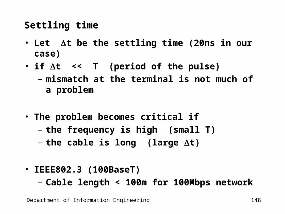
Settling time
• Let t be the settling time (20ns in our case)
• if t << T (period of the pulse)
– mismatch at the terminal is not much of a problem
• The problem becomes critical if
– the frequency is high (small T)
– the cable is long (large t)
• IEEE802.3 (100BaseT)
– Cable length < 100m for 100Mbps network
149Department of Information Engineering
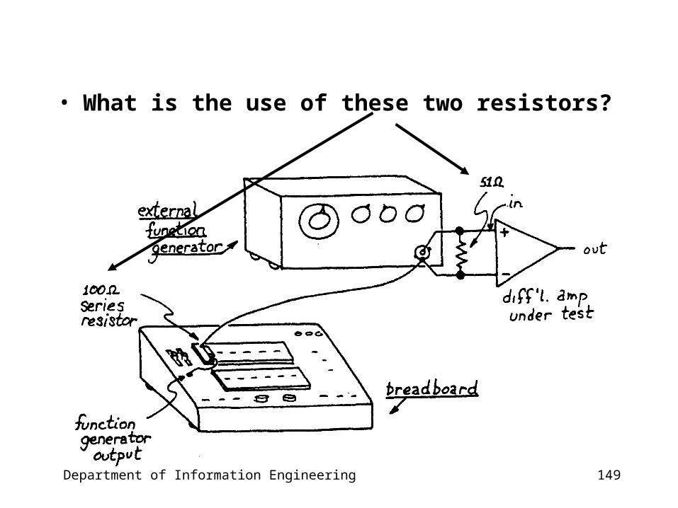
• What is the use of these two resistors?

150Department of Information Engineering
Transmission Line
• 100 ohm
– used to kill any oscillation by reducing the phase shift caused by the cable capacitance
• 51 ohm
– use to terminate the 50 ohm coaxial cable (use 51 ohm because there is no 50 ohm resistor )
151Department of Information Engineering
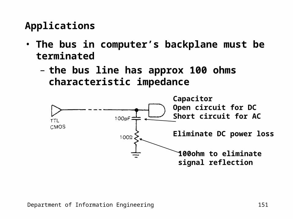
Applications
• The bus in computer’s backplane must be terminated
– the bus line has approx 100 ohms characteristic impedance
Capacitor Open circuit for DCShort circuit for AC
Eliminate DC power loss
100ohm to eliminatesignal reflection
152Department of Information Engineering
Applications
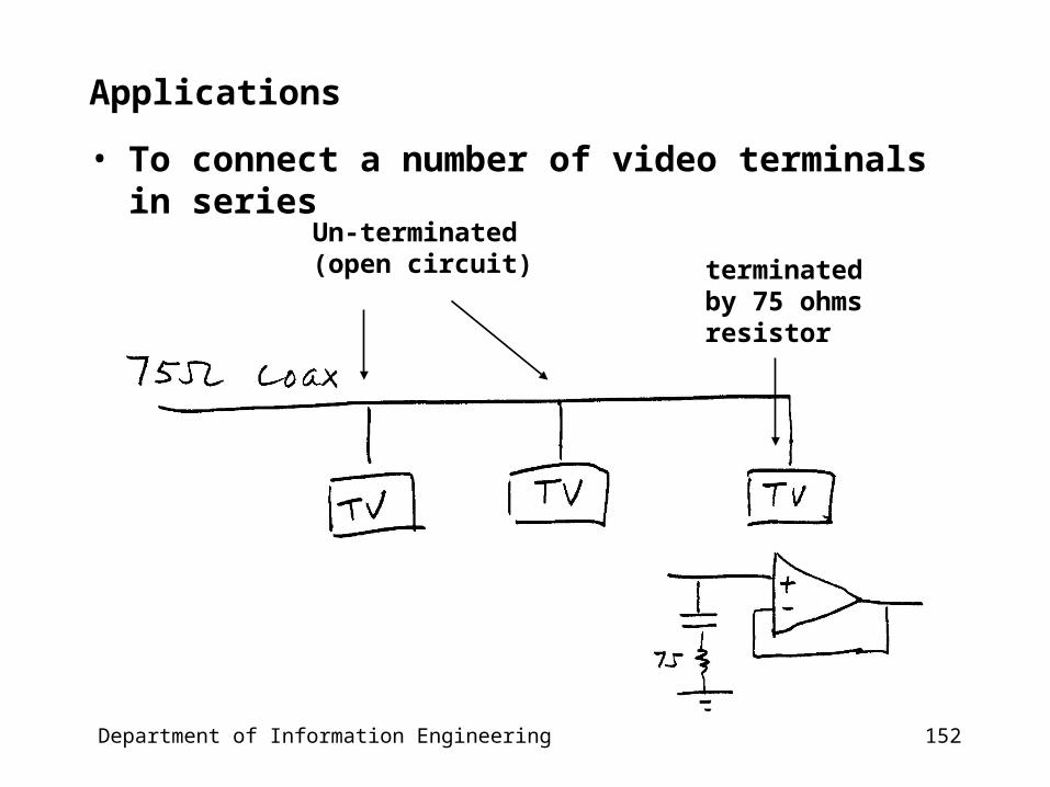
• To connect a number of video terminals in series
Un-terminated(open circuit) terminated
by 75 ohmsresistor
Related Documents


![Medium Voltage Capacitors€¦ · 3 Medium Voltage Capacitors Type MSCE Single Phase Capacitor - Insulation Level 36 kV [50/150] Capacitor without Internal Fuse System Rated Voltage:](https://static.cupdf.com/doc/110x72/5ead95020ebe1a1107404c5b/medium-voltage-3-medium-voltage-capacitors-type-msce-single-phase-capacitor-insulation.jpg)


