1 MUFFAKHAM JAH COLLEGE OF ENGINEERING & TECHNOLOGY Banjara Hills Road No 3, Hyderabad 34 www.mjcollege.ac.in DEPARTMENT OF ELECTRICAL ENGINEERING LABORATORY MANUAL POWER ELECTRONICS LAB For B.E. III/IV (II – SEM) EEE& EIE 2014-15 Prepared by: Mrs.Mahmooda Mubeen (Asst.Prof EED)

Welcome message from author
This document is posted to help you gain knowledge. Please leave a comment to let me know what you think about it! Share it to your friends and learn new things together.
Transcript
1
MUFFAKHAM JAH COLLEGE OF ENGINEERING & TECHNOLOGY
Banjara Hills Road No 3, Hyderabad 34
www.mjcollege.ac.in
DEPARTMENT OF ELECTRICAL ENGINEERING
LABORATORY MANUAL
POWER ELECTRONICS LAB
For
B.E. III/IV (II – SEM) EEE& EIE
2014-15
Prepared by: Mrs.Mahmooda Mubeen
(Asst.Prof EED)

POWER ELECTRONICS LAB, EED
2
MUFFAKHAM JAH COLLEGE OF ENGINEERING & TECHNOLOGY
ELECTRICAL ENGG. DEPARTMENT
LIST OF EXPERIMENT
Power Electronics Lab. (EE-382)
1. SCR, BJT, MOSFET AND IGBT Characteristics.
2. Gate triggering circuits for SCR Using R, RC, UJT.
3. Single Phase Step down Cycloconverter with R and RL loads.
4. A.C. voltage controllers with R and RL loads.
5. Study of forced commutation techniques.
6. Two Quadrant D.C. Drive.
7. 1-Φ Bridge rectifier-half control and full control with R and
RL loads.
8. Buck and Boost choppers.
9. 3-Φ Bridge rectifier-half control with R and loads.
10. Simulation of Single Phase Full converter and Semi converter.
11. Simulation of Single Phase & Three Phase Inverter.
12. Simulation of Single Phase cycloconverter
13. Single Phase Inverter with R & RL Load. MUFFAKHAM JAH COLLEGE OF ENGINEERING AND TECHNOLOGY

POWER ELECTRONICS LAB, EED
3
ELECTRICAL ENGINEERING DEPARTMENT
POWER ELECTRONICS LAB
STATIC CHARACTERISTICS OF SCR
Experiment 1a
Aim: To Study the static characteristics of SCR
Apparatus: SCR characteristic trainer kit
0-25 Volts Dc voltmeter
0-100 mA DC ammeter
CRO
Patch chords
Theory: SCR works in three modes:
1) Forward blocking mode
2) Forward conducting mode
3) Reverse blocking mode
Forward blocking mode:
When anode is positive w.r.t cathode and the gate circuit is open the SCR is forward
biased. A small forward leakage current flows. If the voltage is increased the break down
occurs at a voltage called forward break-over voltage VBO, SCR offers high input
therefore it is treated as open, The SCR is in OFF state.
Forward conducting mode:
In this mode the conduction takes place from anode to cathode with the gate pulse is
applied between gate and cathode, the SCR is turned ON. This is the ON state in which it
behaves as a closed switch. The voltage drop across the device is due to resistive drop in
the four layers.
Reverse blocking mode:
When cathode is positive with respect to anode with gate terminal open the device is in
reverse blocking mode. This is the OFF state. If the reverse voltage is increased, the
brake down occurs at VBR (brake down voltage). The reverse current increases causing
avalanche
The SCR is treated as open switch – OFF state

POWER ELECTRONICS LAB, EED
4
Circuit Diagram:
Observation Table: IG = ----------- mA
Ig (mA) Vak (V)
Procedure:
i) Static Characteristics without GATE pulse
a) Connect the circuit as shown, adjust Dc1 to about 4V
b) Short the gate and the anode terminal.
c) Note down the anode voltage and current VAK and IAK
d) Open the gate terminal and note the holding current for applied DC1 voltage and
observe if the SCR is in the ON state.
e) Repeat the above procedure for different values of DC voltage. Until the SCR
starts conducting.
f) Tabulate and plot VAK Vs IAK
ii) Static Characteristics with GATE pulse
a) Connect as shown, adjust Dc1 to its full value - 20V
b) Keep the gate voltage – DC2 minimum such that the SCR is in the OFF state,
minimum position in anti-clock wise direction
c) Vary the gate current by increasing DC2 until the SCR fires (ON state) which is
indicated by the current through SCR.
d) Tabulate and plot VAK Vs IAK for different values of gate current.
1K pot
12V 470Ώ
A
A
V (0-30V) (0-200mA)
(0-200mA)
470Ώ
1K pot
30V

POWER ELECTRONICS LAB, EED
5
Expected Graphs:
Result: Thus the VI characteristics of SCR are drawn and the values from the
graph sheet are noted down
Latching Current (IL) = -------------
Holding current (IH) = ----------------
Discussion of Result:
Based on the theory discuss the difference between the values of latching
and holding current.
Check for VB O for different gate current to understand the application of
Gate current.
MUFFAKHAM JAH COLLEGE OF ENGINEERING AND TECNOLOGY
ELECTRICAL ENGINEERING DEPARTMENT
Ig2 Ig1
VAK
I AK
Forward Blocking
OFF state
VBO
Forward Blocking
Voltage
Reverse leakage
Current
Reverse Blocking
Reverse
Breakdown
Voltage VBR
Reverse leakage
Current
ON- State
Voltage
Drop
Forward
Conduction
ON - State

POWER ELECTRONICS LAB, EED
6
POWER ELECTRONICS LAB
CHARACTERISTICS OF MOSFET
Experiment 1b
Aim: To study the output and transfer characteristics of MOSFET
Apparatus: Trainers Kit
Ammeter (0-200mA)
Voltmeter (0-20V)
Patch Chords
Circuit Diagram:
Procedure:
Output Characteristics
1) Connect the MOSFET drain – Source terminal to the MOSFET circuit
terminal
2) Connect the ammeter in drain terminal, the voltmeter across the gate source
terminal and another voltmeter across the drain – source terminal
3) Switch ON the supply
4) Fix the gate- source voltage using the pots
5) Smoothly vary the drain-Source terminal (VDS) Voltage by varying the Pot2
till the MOSFET turns ON. Note the Voltmeter and Ammeter readings.
POWER ELECTRONICS LAB, EED
7
6) Vary the VDS and Note change in current ID
7) Note the value of pinch OFF Voltage for different values of VGS
Observations:
a) Output Characteristics:
S.No. VGS (Constant)
VDS ID
Expected Graphs:
Procedure:
Transfer characteristics

POWER ELECTRONICS LAB, EED
8
1) Switch ON the supply
2) Fix the drain- source voltage using the pots
3) Smoothly vary the Gate-Source terminal (VGS) Voltage by varying the Pot2 till
the MOSFET turns ON. Note the Voltmeter and Ammeter readings
4) Vary the VGS and Note change in current ID
5) Note the value of Gate Threshould Voltage for different values of VDS
b) Transfer Characteristics:
S.No. VDS(Constant)
VGS ID
Expected Graphs:

POWER ELECTRONICS LAB, EED
9
Result: The output and transfer characteristics of the MOSFET are studied and graphs plotted.
The pinch off Voltage is --------------------- for VGS = ------------------ and gate threshold voltage
for the transfer characteristics is -------------------------- for VDS = ---------
Discussion of Result:
Observe the Pinch of voltage obtained from output characteristics with
different VGS and comment on the result.
Significance of Gate Threshold voltage in Transfer characteristics.
Mention the device whether it is a voltage controlled or current controlled
MUFFAKHAM JAH COLLEGE OF ENGINEERING AND TECHNOLOGY

POWER ELECTRONICS LAB, EED
10
ELECTRICAL ENGINEERING DEPARTMENT
POWER ELECTRONICS LAB
CHARACTERISTICS OF IGBT
Experiment 1c
Aim: To study the output and transfer characteristics of IGBT
Apparatus: Trainers Kit
Ammeter (0-200mA)
Voltmeter (0-20V)
Patch Chords
Circuit Diagram:
Procedure:
Out-Put Characteristics
6) Connect the collector, emitter and the gate terminals to the characteristics
circuit
7) Connect the ammeter to measure the collector current

POWER ELECTRONICS LAB, EED
11
8) Connect a voltmeter across the gate -emitter and another voltmeter across the
collector – emitter terminals
9) Switch ON the 230V AC supply
10) Fix the gate- emitter voltage (V GE) using the pot1
11) Smoothly vary the Collector-Emitter (VCE) Voltage by varying the Pot2 till the
IGBT turns ON. Note the Voltmeter and Ammeter (IC) readings
12) Once turned ON, Increase the VCE and Note change in current IC
13) Repeat the steps 5 & 6 for different values of VGE
14) Note the value of pinch OFF Voltage from the graph
Observations:
a) Output Characteristics:
S.No. VGE (Constant)
VCE IC
Expected Graphs:
Output characteristics
POWER ELECTRONICS LAB, EED
12
Transfer Characteristics:
15) Keep the V CE constant using pot2
16) Vary VGE using pot1 to trigger the IGBT, Note the values of VGE and IC
17) Smoothly increase the value of VGE and not the values of voltage and current
18) Plot VGE Vs IC , Note the threshold value of voltage from the graph
19) Repeat for different values of VCE
Observations:
b) Transfer Characteristics:
S.No. VCE(Constant)
VGE IC
Expected Graphs:
Transfer Characteristics

POWER ELECTRONICS LAB, EED
13
Result: The output and transfer characteristics of the IGBT are studied and graphs plotted. The
threshold Voltage is --------------------- fos VGE = ------------------ and that for the transfer
characteristics it s -------------------------- for VCE = ----------.
Discussion of Result:
Observe the Pinch of voltage obtained from output characteristics with
different VGE and comment on the result.
Significance of Gate Threshold voltage in Transfer characteristics.
Mention the device whether it is a voltage contr olled or current
controlled.

POWER ELECTRONICS LAB, EED
14
MUFFAKHAM JAH COLLEGE OF ENGINEERING AND TECHNOLOGY
ELECTRICAL ENGINEERING DEPARTMENT
POWER ELECTRONICS LAB
R, RC, UJT Firing of SCR
Experiment:2
Aim: To Study the operation of resistance firing circuit using R, RC & UJT firing module.
Apparatus: R, RC & UJT firing module.
CRO, 50V/4A Rheostat
Digital Multi-meter
Patch chords
Theory: R-Firing
The gate current is used for triggering instead of the gate pulse. In the circuit
shown, when the gate current Ig is minimum, the SCR turns ON and the supply
voltage Vs goes positive Swhile VL goes negative such that Vs is almost equal to
the load voltage VL.
As Vs goes negative, SCR turns OFF and the load voltage VL is Zero
The diode prevents the gate cathode current reverse bias during the negative half
cycle.
Same sequence is repeated during the positive half cycle – VS goes positive.
R is varied to vary the load voltage
RV will vary the firing angle
Rmin limits the value of the gate current while varying RV
Rb should be such that it causes minimum voltage drop across it so that it does not
exceed maximum gate voltage.
Circuit Diagram: R-Firing
Ph
N
Load
Rheostat
R min
R b
SCR 24 V
Supply
50 Ω /
4A
D R y
(Out)

POWER ELECTRONICS LAB, EED
15
Procedure:
R-Firing
1. Connect the input supply to the trainer module
2. Connect P & N terminals to T7 & T9
3. Connect one end of the load rheostat to P terminal of 24V AC supply
4. Connect the other end of the load rheostat to N terminal of 24V AC supply
5. Connect the cathode (K) to the N terminal of SCR
6. Connect G & K terminals of firing circuit to G & K of SCR
7. Connect CRO ground to anode of SCR. Connect a Probe to T7 and another probe to
cathode of SCR
8. Switch ON the supply, Power ON/OFF switch, 24V ac Switch, Supply to CRO
9. Observe the waveform for input AC voltage & load voltage for different firing angles
10. Plot the waveforms
11. Measure the DC voltage across the load & rms value of the input voltage using a
multi-meter.
12. Calculate the output voltage Vdc = (√2V / 2п)(1+cosα)
13. Compare the two values.
Observation Table:
Vrms T(msec) t (msec) α (degrees) Vo(measured) Vo(cal)
=𝐕𝐦
𝟐п(1+cosα) V
25.4
3.2
0 0
11.18
11.43
Model Calculation:
Vm = Vrms*√2
Vo (calculated) = Vm
2п (1+cosα) V
= 25.4∗√2
2п (1+cos 0
)
Vo = 11.43V

POWER ELECTRONICS LAB, EED
16
Theory:
RC- Firing
When VS goes positive and the capacitor voltage VC is equal to the gate triggering voltage
Vgt where (Vgt = Vgmin + VD1), the SCR will turn ON. The capacitor holds a small value of
voltage. During positive half cycle the capacitor charges through D2 .The diode D1 prevents
break down of the gate to cathode junction during negative half cycle.
Circuit Diagram:
RC-Firing
Ph
N C
Procedure:
RC-Firing
1. Connect the input supply to the trainer module
2. Connect P & N terminals to T12 & T13
3. Connect one end of the load rheostat to P terminal of 24V AC supply
4. Connect the other end of the load rheostat to N terminal of 24V AC supply
5. Connect the cathode (K) to the N terminal of SCR
6. Connect G & K terminals of firing circuit to G & K of SCR
7. Connect CRO ground to anode of SCR. Connect a Probe to T7 and another probe to
cathode of SCR.
R y
(Out)
D
50 Ω / 4A
Load
Rheostat
SCR 24 V Supply

POWER ELECTRONICS LAB, EED
17
8. Switch ON the supply, Power ON/OFF switch, 24V ac Switch, Supply to CRO
9. Observe the waveform for input AC voltage & load voltage for different firing angles
10. Plot the waveforms
11. Measure the DC voltage across the load & rms value of the input voltage using a
multi-meter.
12. Calculate the output voltage Vdc = (√2V / 2п)(1+cosα)
13. Compare the two values.
Observation Table:
Vrms T(msec) t (msec) α (degrees) Vo(measured) Vo(cal) =
𝐕𝐦
𝟐п(1+cosα)
V
25.6
3.2
0.2 11.25
11.11
11.41
Model Calculation:
Vm = Vrms*√2
Vo (calculated) = Vm
2п (1+cosα) V
= 25.6∗√2
2п (1+cos 11.25
)
Vo = 11.41V

POWER ELECTRONICS LAB, EED
18
EXPECTED GRAPH:
R, RC Firing Circuit
Theory:
UJT- Firing
Is also known as Ramp triggering. The diodes D1 - D4 rectifies the input AC to Dc. The Zener
diode Z is used to clip the rectified voltage to a standard level VZ which remains constant
except when Vdc is zero.
The Zener voltage VZ is applied to the charging circuit RC. The capacitor C charges by
current i1. When the capacitor voltage reaches the threshold voltage ηVZ, the Emitter-base1
junction breaks down and C charges through the primary of the pulse transformer sending
current i2.When i2 is positive the SCR turns ON. The rate of rise of capacitor voltage can be
varied using R. The firing angle can be controlled up to 1500 .
It can be used in Single phase controller, single phase half wave controlled converter,
single phase controlled bridge rectifier, etc
POWER ELECTRONICS LAB, EED
19
Circuit Diagram :
s
Procedure:
1. Connect the input supply to the trainer module
2. Connect one end of the load rheostat to A of the SCR
3. Connect the other end of the load rheostat to P terminal of 24V AC supply
4. Connect G1 & K1 terminals of UJT firing circuit to G & K of SCR
5. Switch ON the supply, Power ON/OFF switch, 24V ac Switch, Supply to CRO
6. Observe the waveform for input AC voltage & Pulsating DC voltage
7. Observe the Zener diode voltage( T4) & capacitor voltage (T5)
8. Plot the waveforms
9. Repeat the experiment for various firing angles
Observation Table:
Vrms T(msec) t (msec) α (degrees) Vo(measured) Vo(cal)
=𝐕𝐦
𝟐п(1+cosα) V
25.8
3.2
0.4 10.78
10.99
11.5

POWER ELECTRONICS LAB, EED
20
Model Calculation:
Vm = Vrms*√2
Vo (calculated) = Vm
2п (1+cosα) V
= 25.8∗√2
2п (1+cos 10.78
)
= 11.5V
Expected graphs:
UJT Firing

POWER ELECTRONICS LAB, EED
21
Results: The wave forms for the R, RC, and UJT firing of the SCR are studied and plotted.
Discussion of Result:
Analyze the output voltage waveform for different firing circuits and mention the
limitation of each circuit.
In all triggering circuits comment on firing angle vs output voltage.

POWER ELECTRONICS LAB, EED
22
MUFFAKHAM JAH COLLEGE OF ENGINEERING AND TECHNOLOGY
ELECTRICAL ENGINEERING DEPARTMENT
POWER ELECTRONICS LAB
SINGLE PHASE CYCLOCONVERTER
Experiment: 3
Aim: To Study the operation of cyclo-converter and observe the output waveforms.
Apparatus Required: Cyclo-converter Kit, CRO & Patch cords.
Theory:
In the cycloconverter one group of thyristers produce positive polarity of the load voltage and the
other group produces the other polarity. One group of SCRs are gated together. Depending on
the polarity of the input only one of them will conduct. When P is positive w.r.t O then SCR1
will conduct otherwise SCR2 will conduct. Thus in both half cycles of the input the load voltage
will be positive. The SCRs get turned OFF by natural commutation at the end of every half
cycle.
Depending on the desired frequency, gating pulses to positive group of SCRs will
be stopped and SCRs 3 & 4 will be gated SCR 3 conducts when p is +ve and SCR4 conducts
when P is –ve.
Circuit Diagram:

POWER ELECTRONICS LAB, EED
23
Block Diagram:
Procedure:
1. Keep all the switches in the OFF position.
2. Connect the banana connector as given below
A1 to K3& 24V AC output
A2 to K4& 24V AC output
A3 to K1 & L1
A4 to K2& L3
R2 to L2
Out put of 0V to R1
G1 to G1
G2 to K2
G3 to K3
G4 to K4 and
K1 to K1
3. Select the output frequency level from the table given below
SA SB Frequency in Hz
0
1
1
0
1
1
0
0
12.5
16.67
25
50

POWER ELECTRONICS LAB, EED
24
4. Switch ON the trainer kit using Power ON/OFF switch
5. Switch ON the pulse release switch
6. Switch ON the 24V AC output
7. Vary the control voltage (Vc) to vary the firing angle, Observe the
Waveforms.
Expected Graphs:

POWER ELECTRONICS LAB, EED
25
Results: The output of the cyclo converter for f, f/2 , f/3 and f/4 have been studied.
Discussion of Result:
Comment on Time Period and frequency with reference to input frequency for different
levels of output frequency.
POWER ELECTRONICS LAB, EED
26
MUFFAKHAM JAH COLLEGE OF ENGINEERING AND TECHNOLOGY
ELECTRICAL ENGINEERING DEPARTMENT
POWER ELECTRONICS LAB
SINGLE PHASE AC VOLTAGE CONTROLLER
Experiment : 4
Aim: To study the operation of an AC single phase voltage controller with R and RL load
Apparatus: Trainer Kit
CRO
Patch chords
Theory:
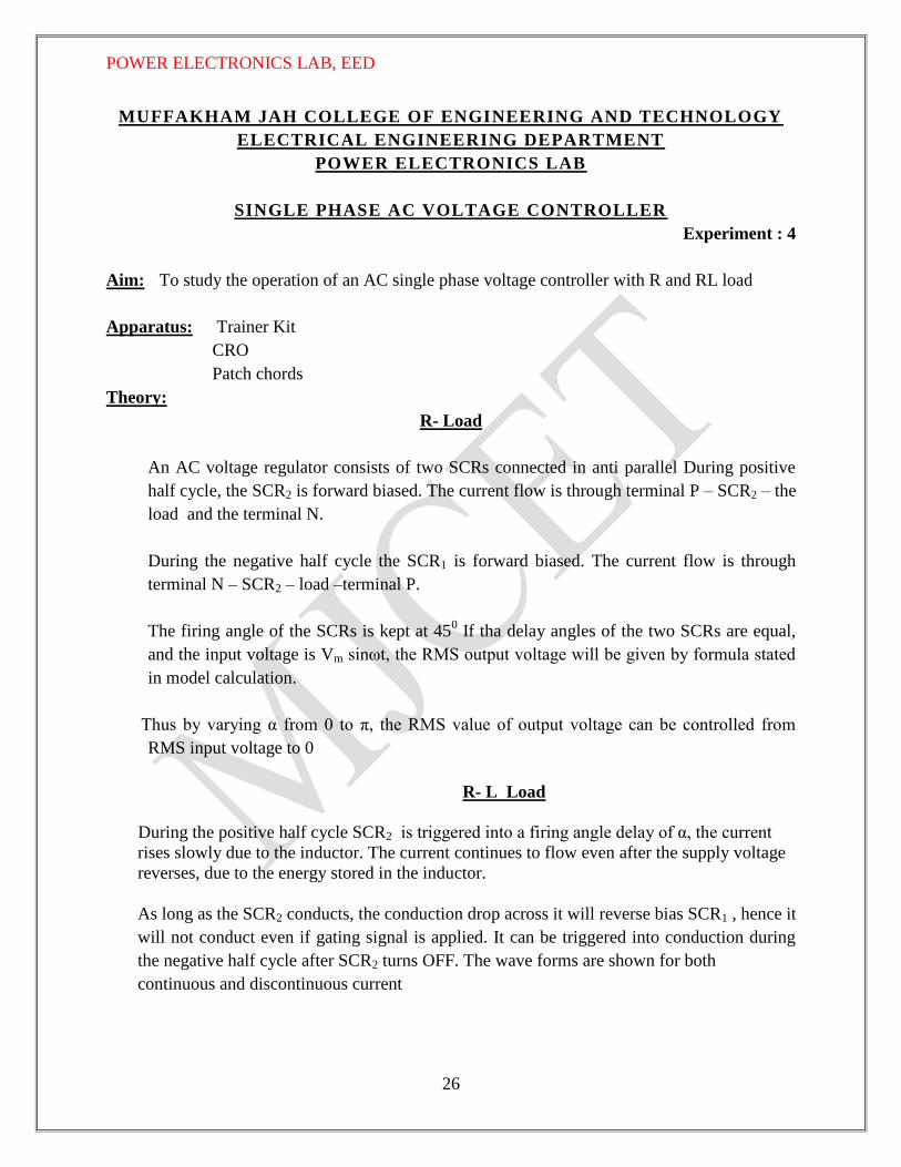
R- Load
An AC voltage regulator consists of two SCRs connected in anti parallel During positive
half cycle, the SCR2 is forward biased. The current flow is through terminal P – SCR2 – the
load and the terminal N.
During the negative half cycle the SCR1 is forward biased. The current flow is through
terminal N – SCR2 – load –terminal P.
The firing angle of the SCRs is kept at 450 If tha delay angles of the two SCRs are equal,
and the input voltage is Vm sinωt, the RMS output voltage will be given by formula stated
in model calculation.
Thus by varying α from 0 to π, the RMS value of output voltage can be controlled from
RMS input voltage to 0
R- L Load
During the positive half cycle SCR2 is triggered into a firing angle delay of α, the current
rises slowly due to the inductor. The current continues to flow even after the supply voltage
reverses, due to the energy stored in the inductor.
As long as the SCR2 conducts, the conduction drop across it will reverse bias SCR1 , hence it
will not conduct even if gating signal is applied. It can be triggered into conduction during
the negative half cycle after SCR2 turns OFF. The wave forms are shown for both
continuous and discontinuous current

POWER ELECTRONICS LAB, EED
27
Circuit Diagram:
R-Load
R-L Load
V1
120 Vrms
50 Hz
0Deg
D1
2N1599
D4
2N1599 R1
500Ω
V1
120 Vrms
50 Hz
0Deg
D1
2N1599
D4
2N1599
R1
500Ω
L1
100mH

POWER ELECTRONICS LAB, EED
28
Procedure:
R –Load
1. Connect anode of SCR2 to the cathode of SCR1
2. Connect the 24V AC positive terminal to anode of SCR2
3. Connect R load terminal between cathode of SCR1 and 24V AC output.
4. Connect the CRO across the load
5. Connect the voltmeter across the load terminals
6. Connect G2 & K2 of firing circuit to G2 & K2 of SCR 2
7. Switch ON the trainer kit
8. Place the switch S2 in SCR mode
9. Switch ON the 24V AC supply
10. Switch ON the denounce switch.
11. Note down the peak value of voltage Vm , triggering angle α and conduction
angle γ
12. By varying the firing angle the output can be varied
13. Plot the graph Vm versus α and γ
RL – Load
1. Connect R and L in series then connect the load terminals between cathode of
SCR1 and 24V ac input.
2. Repeat the above steps
3. Observe the waveforms
Observation Table:
R – Load
SNo Input
Voltage
Firing Angle
α
Measured
Output
Calculated
Output
1. 22.98V 56.25° 19.2V 20.99V

POWER ELECTRONICS LAB, EED
29
Model Calculation:
Vm = Vrms*√2
𝑽𝒐(𝒄𝒂𝒍) =𝑽𝒎
√𝟐
𝝅 − 𝜶
𝝅 +
𝒔𝒊𝒏 𝟐𝜶
𝟐𝝅
*Vo calculated is RMS voltage across output.
𝑽𝒐(𝒄𝒂𝒍) =𝟐𝟐.𝟗𝟖 ∗ √𝟐
√𝟐
𝝅 − 𝟎.𝟗𝟖𝟏
𝝅 +
𝒔𝒊𝒏 𝟐(𝟓𝟔.𝟐𝟓)
𝟐𝝅
𝑽𝒐 = 20.99 (56.25°= 0.981radians)
RL – Load
SNo Input
Voltage
Firing Angle
α
Extinction
angle β
Measured
Output
Calculated
Output
1. 23.33 𝟓𝟔.𝟐𝟓° 𝟏𝟗𝟔.𝟖𝟏° 20.7V 21.36V
Model Calculation:
𝑽𝒐 𝒄𝒂𝒍 = 𝑽𝒎 𝟏
𝟐𝝅 𝜷 − 𝜶 +
𝒔𝒊𝒏 𝟐𝜶
𝟐−𝒔𝒊𝒏 𝟐𝜷
𝟐
𝑽𝒐 𝒄𝒂𝒍 = 𝟐𝟑.𝟑𝟑 ∗ √𝟐 𝟏
𝟐𝝅 𝟐.𝟒𝟓 +
𝒔𝒊𝒏 𝟐 ∗ 𝟓𝟔.𝟐𝟓°
𝟐−𝒔𝒊𝒏 𝟐 ∗ 𝟏𝟗𝟔.𝟖𝟏°
𝟐
𝑽𝒐 = 21.36V
where : 𝜷 − 𝜶 = 𝟏𝟗𝟔.𝟖𝟏° − 𝟓𝟔.𝟐𝟓° = 𝟏𝟒𝟎.𝟓𝟓°
=2.45 radians

POWER ELECTRONICS LAB, EED
30
Expected graphs:

POWER ELECTRONICS LAB, EED
31
Simulation Results:
R-Load
RL-Load
Results: The SCR based single phase AC voltage controller or regulator with R & RL load is
studied and the required graphs are plotted.
Discussion of Result:
Mention the Purpose of Ac voltage controller.
Analyze the effect of change in firing angle on output Voltage waveform.
Compare the Theoretical values of Output voltage with Practical values with different
firing angles.
POWER ELECTRONICS LAB, EED
32
MUFFAKHAM JAH COLLEGE OF ENGINEERIN G AND TECHNOLOGY
ELECTRICAL ENGINEERING DEPARTMENT
POWER ELECTRONICS LAB
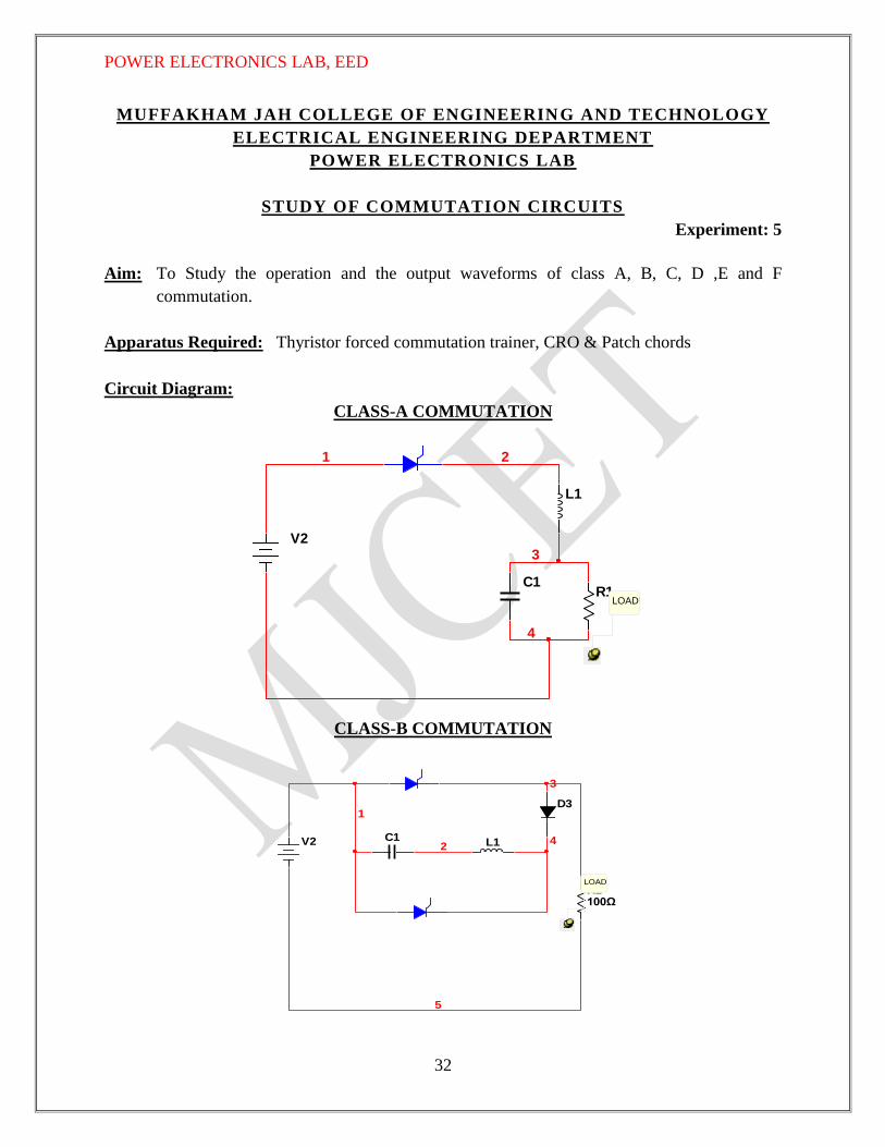
STUDY OF COMMUTATION CIRCUITS
Experiment: 5
Aim: To Study the operation and the output waveforms of class A, B, C, D ,E and F
commutation.
Apparatus Required: Thyristor forced commutation trainer, CRO & Patch chords
Circuit Diagram:
CLASS-A COMMUTATION
CLASS-B COMMUTATION
D1
2N1597
C1
1F
V1
0 V 10 V
10msec 20msec
V2
12 V
1
R1
10Ω
L1
100uH
XSC1
A B
Ext Trig+
+
_
_ + _
03
2
4
LOADUser (2016-01-05):
D1
2N1597
C1
10uF
V1
0 V 10 V
10msec 20msec
V2
12 V
L1
100uH
XSC1
A B
Ext Trig+
+
_
_ + _
0
D2
2N1597
R1100Ω
D3
DIODE_VIRTUAL
V3
0 V 10 V
10msec 20msec
1
2
3
4
5
LOADUser (2016-01-05):

POWER ELECTRONICS LAB, EED
33
CLASS-C COMMUTATION
CLASS-D COMMUTATION

POWER ELECTRONICS LAB, EED
34
CLASS-E COMMUTATION
CLASS-F COMMUTATION
Procedure:
CLASS A: Connect G1 of triggering circuit to G1 of the power circuit
Connect K1 of triggering circuit to K1 of the power circuit
Connect +15V to A1 terminal of SCR1
Connect K1 of SCR to inductor L1
Connect another end of L1 to C2 and resistance Rl2
Connect other end of capacitor C2 & Resistance RL2 to – 15 V DC
Connect CRO probe across the resistor RL2.
Switch on the trainer kit ON/OFF switch, 15V Dc Supply, auxiliary switch of the
SCR and the main SCR switch.
Slowly vary the frequency knob and observe the waveforms & Plot them
C1
60mF
D12N1597
L1
1mH
T1
NLT_PQ_4_10
R1
100Ω
V1
12 V
V2
0 V 10 V
10msec 20msec
2
XSC1
A B
Ext Trig+
+
_
_ + _ 0
3
1
4
EXTERNAL PULSE:
V1
120 Vrms
50 Hz
0Deg
R1
100Ω
D1
2N1597

POWER ELECTRONICS LAB, EED
35
CLASS B: Connect G1 of triggering circuit to G1 of the power circuit
Connect K1 of triggering circuit to K1 of the power circuit
Connect G2 of triggering circuit to G2 of the power circuit
Connect K2 of triggering circuit to K2 of the power circuit
Connect +15V, A1of SCR1, A2 of SCR2, C1 & C2.
Connect the other end of C1 to inductor L1 through C2
Connect another end of L1 to anode of D1
Connect the cathode of D 1 to cathode K1 of SCR1 through resistance Rl2
Connect other end of Resistance RL1 to – 15 V DC
Connect CRO probe across the resistor RL1.
Switch on the trainer kit ON/OFF switch, 15V Dc Supply, auxiliary switch of the
SCR and the main SCR switch.
Fix the frequency knob at certain value, vary the duty cycle knob step by step, and
observe the waveforms & Plot them.
Connect G2 of triggering circuit to G2 of the power circuit
Connect K2 of triggering circuit to K2 of the power circuit
CLASS C: Connect G1 of triggering circuit to G1 of the power circuit
Connect K1 of triggering circuit to K1 of the power circuit
Connect G2 of triggering circuit to G2 of the power circuit
Connect K2 of triggering circuit to K2 of the power circuit
Connect the +15V to one end of RL1& RL2
Connect the capacitor C1 to the other end of RL1& RL2
Connect the anode of SCR2 to RL2
Connect the K1 of SCR1 to K2 of SCR2
Connect K1of SCR1 to +15V
Connect the CRO across RL1
Switch on the trainer kit ON/OFF switch, 15V Dc Supply, auxiliary switch of the
SCR and the main SCR switch.
Fix the frequency knob at certain value, vary the duty cycle knob step by step, and
observe the waveforms & Plot them
CLASS D: Connect G1 of triggering circuit to G1 of the power circuit
Connect K1 of triggering circuit to K1 of the power circuit
Connect G2 of triggering circuit to G2 of the power circuit
Connect K2 of triggering circuit to K2 of the power circuit
Connect +15V DC to K1of SCR1 and C1
Connect other end of C1 to A2of SCR2 and Anode of the diode D1
Connect the cathode of D1 to K2 of SCR2 through the inductor L1
POWER ELECTRONICS LAB, EED
36
Also connect the K1 OF SCR1 to load resistor RL1
Connect K1of SCR1 to +15V and Connect the CRO across RL1
Switch on the trainer kit ON/OFF switch, 15V Dc Supply, auxiliary switch of the
SCR and the main SCR switch.
Fix the frequency knob at certain value, vary the duty cycle knob step by step, and
observe the waveforms & Plot them.
CLASS E: Connect G1 of triggering circuit to G1 of the power circuit
Connect K1 of triggering circuit to K1 of the power circuit
Connect +15V to A1 terminal of SCR1 and to capacitor C1
Connect other terminal of C to Load and external pulse P2.
Connect K1 of SCR1 to external pulse P1.
Switch on the trainer kit ON/OFF switch, 15V Dc Supply, auxiliary switch of the
SCR1.
Fix the frequency knob at certain value, vary the duty cycle knob step by step, and
observe the waveforms & Plot them
CLASS F: Connect G1 of triggering circuit to G1 of the power circuit
Connect K1 of triggering circuit to K1 of the power circuit
Connect 9V AC, (A1) SCR1 and RL1 in series.
Connect CRO across RL1
Switch ON the Kit, 9V AC and observe the waveforms
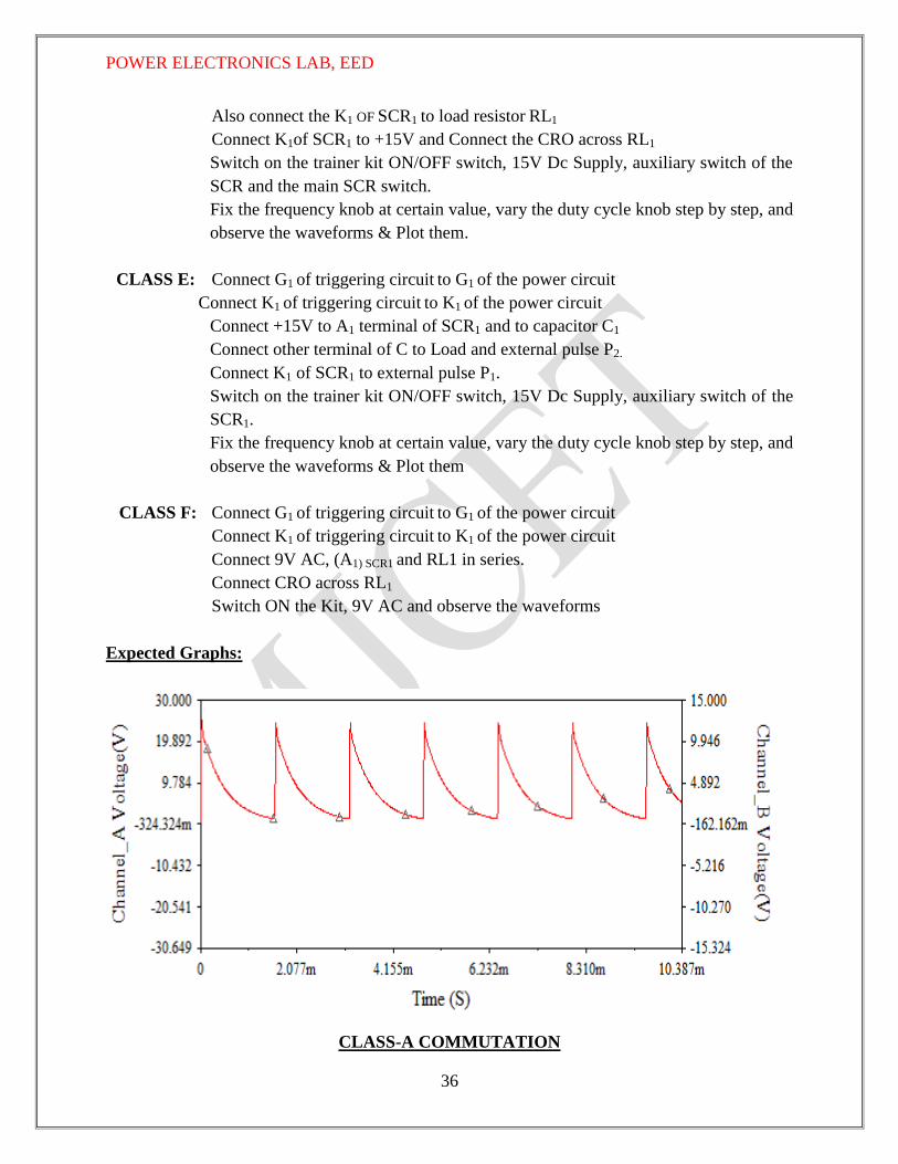
Expected Graphs:
CLASS-A COMMUTATION

POWER ELECTRONICS LAB, EED
37
CLASS-B COMMUTATION
CLASS-C COMMUTATION

POWER ELECTRONICS LAB, EED
38
CLASS-D COMMUTATION
CLASS-E COMMUTATION

POWER ELECTRONICS LAB, EED
39
CLASS-F COMMUTATION
Results: The output waveforms of the forced commutation and natural commutation are
observed.
Discussion of Result:
Differentiate between forced commutation and natural commutation
Analyze the output voltage waveform for different commutation Techniques
Specify in what category each class(A, B, C, D, E, F) lies.

POWER ELECTRONICS LAB, EED
40
MUFFAKHAM JAH COLLEGE OF ENGINEERING AND TECHNOLOGY
ELECTRICAL ENGINEERING DEPARTMENT
POWER ELECTRONICS LAB
STUDY OF AN IGBT BASED TWO QUADRANT DC DRIVE
Experiment :6
Aim: To study the IGBT based four quadrant chopper DC drive.
.
Apparatus: IGBT based four quadrant chopper DC drive trainer set
Probe Patch Chord
DC Motor
CRO
Circuit Diagram:
IL
A B
Load
Vo
io io
Vo
II Quadrant
Regeneration
T
3
T
4
T
1
T
2
D
3
D
4
D
1
D
2
V
dc
I Quadrant
Power Positive
IV Quadrant
Regeneration
Power Negative
III Quadrant
Power Positive

POWER ELECTRONICS LAB, EED
41
Theory: The chopper controlled circuit can operate in four quadrants of the V-I plane. The out
put voltage and current can be controlled in both magnitude and direction. In the first quadrant
the power flows from source to load and is positive. In the second quadrant the voltage is
positive but the current is negative. Thus the power flows from load to source, in case of
inductive loads. In third quadrant both voltage and current are negative hence the power flows
from source to load. In the fourth quadrant, the current is positive and the voltage is negative
thus the power is negative.
When the diodes are connected in anti-parallel with the thyristers it is called the full-bridge
converter topology. The input voltage is constant; the output can be a variable DC voltage. Thus
it is also called a DC-DC converter. When a gating signal is applied to the SCR, either the SCR
or the diode will conduct depending on the direction of the output current.
Procedure:
Connect the power module and the controller module to the AC supply.
Connect the pwm output of the controller module to the pwm input of the power
module using a pulse cable
Connect the field terminal of the DC motor to the F + and F- and the armature
terminals to A+ and A – terminals of the power module.
Switch ON the power supply in both IGBT power module and the controller module.
o Select S2 at SCM( speed control mode) and S1 at open loop
o Keep the armature pot at minimum and S3 at ON position.
o Keep the field pot maximum.
Reset the controller module using S4
SCM Mode: The LCD will display the following one by one with a delay
of few seconds.
Select the forward option with I quadrant switch, The display will show
Speed control Mode
(SCM)
I. Forward
II. Reverse
D.C Drive (CW)
D.CY.Field = 80%
D.CY. Armature = 50%
Actual speed = 0

POWER ELECTRONICS LAB, EED
42
Vary the armature duty cycle pot such that the motor runs in the selected
direction and at a speed corresponding to the duty cycle .
Select the reverse option using II quadrant switch, now the display will be
FCM mode: Keep the switch S 1 in FCM mode (Four quadrant chopper
control mode)
Keep armature pot at min, and field pot at maximum.
Select I Quadrant
Reset the controller using S 4 , Select forward running.
Vary the armature pot to vary the speed of the motor
Apply forward braking using II quadrant key.
Reset the controller with S4
Select III quadrant
Vary the speed of the motor using the armature pot
Apply Reverse braking using IV quadrant key
Results: The four quadrant operation of the DC motor is studied.
Discussion of Result:
Comment on Forward Running, Forward Braking, Reverse Running, Reverse
Braking.
D.C Drive (CW)
D.CY.Field = 80%
D.CY. Armature = 56%
Actual speed = 2
D.C Drive (CW)
D.CY.Field = 80%
D.CY. Armature = 56%
Actual speed = 2
I. Forward Running
II. Forward Braking
I quadrant
III quadrant
III. Reverse Running
IV. Reverse Braking

POWER ELECTRONICS LAB, EED
43
MUFFAKHAM JAH COLLEGE OF ENGINEERING AND TECHNOLOGY
ELECTRICAL ENGINEERING DEPARTMENT
POWER ELECTRONICS LAB
SINGLE PHASE BRIDGE RECTIFIER
Experiment: 7
Aim: To Study the Single phase full wave bridge rectifier (Half and Full Controlled) with R
load
Apparatus: Single Phase bridge rectifier Module
Single Phase Triggering Module
Multimeter, Rheostat (220Ω)
CRO, DC motor, Tachometer, Isolation Transformer & Auto-transformer
Patch chords
Theory: Phase control thyristors can control the output voltage of a rectifier, by varying
the firing angle or delay angle α of the thyristor. In phase control thyristor
commutation or turning OFF takes place by line or natural commutation. It has
applications in industrial variable speed drives from very low to very high power
levels as high as few Mega watts. The output is fed to DC motor to control the
speed by varying the voltage.
Circuit Diagram:
Half Controlled Bridge Rectifier

POWER ELECTRONICS LAB, EED
44
Full Controlled Bridge Rectifier
Procedure:
a) Make the connection as per the circuit diagram
b) Keep control voltage potentiometer at minimum position and set all the switches in
OFF position
c) Connect the supply across the line and neutral terminal of the device module
d) Connect the firing pulse from the single phase firing circuit into single phase
triggering module in a sequence G-G and K-K
e) Connect the cathode terminal K1 –K3 of SCR 1 and SCR3
f) Connect the anode terminals A2-A4 of SCR 2 and SCR4
g) Connect the resistance terminal to A2-and K3
h) Connect the voltmeter across the motor (load )terminals
i) Switch ON the single Phase triggering module
j) Switch ON the MCB
k) Switch ON the De-bounce logic switch

POWER ELECTRONICS LAB, EED
45
l) Adjust the control voltage by using potentiometer
m) Tabulate the speed and motor voltage and plot the graph for R and RL(motor)
Observations: Full & Half Controlled Bridge Rectifier
Vrms T(msec) t (msec) α (degrees) Vo(measured) Vo(cal)
= 𝐕𝐦 п (1+cosα)
V
28.9
5.1
1 35.29
22.2
23.62
Model Calculation:
Vm = Vrms*√2
Vo (calculated) = Vm
п (1+cosα) V
= 28.9∗√2
п (1+cos 35.29)
Vo = 23.62V
Precautions:
1) Set all the switches to the OFF positions
2) To switch ON and OFF the supply voltage correct sequence
3) Perform the experiment with supply voltage less than 55V AC for resistive loads
4) Use isolation Transformer

POWER ELECTRONICS LAB, EED
46
Expected graphs:
Vin
`
Vout
(α =0)
Vout
(α = 45)
Half & Full Controlled Bridge Rectifier.
Results: The output waveforms of the across the load and the SCR are observed and plotted.
Simulation Results: R-Load
Discussion of Result:
Mention the Purpose of Rectifier
Analyze the effect of change in firing angle on output Voltage waveform.
Compare the Theoretical values of Output voltage with Practical values with different
firing angles.
α

POWER ELECTRONICS LAB, EED
47
MUFFAKHAM JAH COLLEGE OF ENGINEERING AND TECHNO LOGY
ELECTRICAL ENGINEERING DEPARTMENT
POWER ELECTRONICS LAB
DC-DC BUCK-BOOST CONVERTER
Experiment: 8a
Aim: To study the open loop response of a buck – boost converter with line and load regulation.
Apparatus: DC-DC Converter trainer Kit
Pulse Patch Chord
Rheostat
CRO
Multimeter
Circuit Diagram:
Buck Converter
Procedure-A : Line Regulation (OPEN LOOP)
Buck operation (Set pulse voltage to 50% ie 2.7V) & for Boost operation (Set
pulse voltage max-100% ie. 4.6V)
1. Connect the P8 of PWM generator to the PWM input of Buck-Boost Converter
Circuit

POWER ELECTRONICS LAB, EED
48
2. Connect the feedback voltage of buck-boost converter circuit to feed back volt input
PWM generator
3. Connect the CRO at T3
4. Connect the 0-30V DC RPS across P1 & P2 Switch ON the AC power supply
5. Switch on the power ON/OFF switch
6. View the carrier signal in the CRO, at T3.
7. Set the switch SW1 in downward position, SW2 in upward direction and view the
PWM signal at T1 as in fig 2. The duty cycle may be changed by changing the SET
VOLTAGE.
8. Switch ON the DC 15V supply
9. View the following wave forms
a. Device Current IQ across I1 & I2
b. Diode current ID across I3 & I4
c. Inductor Current IL across I3 & I7
d. Device Voltage VQ across I2 & I3
e. Rectified Voltage across I5 & I8
f. Inductor voltage VL across I7 & I8
g. The feed back signal at T6
10. Connect the CRO across P5 & P6 to view the output voltage.
Observation Table:
Line Regulation
Vary input voltage below and above 15V
Set voltage: 2.7V (Buck operation )
Model Calculation:
T = TON +TOFF
= 22𝜇s +33 𝜇s = 55 𝜇s
D = TON / T
= 22/55 =0.4
S.no Input Voltage
Vin
TON TOFF D= TON/T Output
Voltage
Measured(Vo)
Output calculated
Vo= [D/(1-D)]*Vs
1 3V 22𝜇s 33 𝜇s 0.4 1.66V 1.98V

POWER ELECTRONICS LAB, EED
49
Vo (calculated) = [D/(1-D)]*Vs
= 0.4/(1-0.4)]*3
Vo =1.98V
Set voltage: 4.6V (Boost operation )
S.no Input Voltage
Vin
TON TOFF D= TON/T Output
Voltage
Measured(Vo)
Output calculated
Vo= [D/(1-D)]*Vs
1 3V 41𝜇s 10 𝜇s 0.8 9.72V 12V
Model Calculation:
T = TON +TOFF
= 41𝜇s +10 𝜇s = 51 𝜇s
D = TON / T
= 41/51 =0.4
Vo (calculated) = [D/(1-D)]*Vs
= 0.8/(1-0.8)]*3
Vo =12V
Procedure-B:
Load Regulation
1. Connect the rheostat bet P5 and P6
2. Connect an ammeter in series with the rheostat
3. For 0 external resistance the output is 5V, (IL=.3-.7Amp)
4. vary the resistance till the load current is 0.7Amp
5. Tabulate the measured readings

POWER ELECTRONICS LAB, EED
50
Observation Table :
Load Regulation
SET Input voltage = 15V
Vary the rheostat for (IL = 0.3 to 0.7)
Measure and tabulate the following readings.
Set pulse voltage: 2.7V (Buck operation )
Input
Voltage
Vin
TON TOFF D= TON/T
(T= TON+ TOFF)
Load
Resistor
(R Ω)
IL(mamps) Output
Voltage
Measured(Vo)
Output calculated
Vo= I*R(volts)
15 24𝜇s 38 𝜇s 0.38 59.2 156 9.21 9.23
Model Calculation:
T = TON +TOFF
= 24𝜇s +38 𝜇s = 62 𝜇s
D = TON / T
= 24/62 =0.38
Vo (calculated)= I*R(volts)
= 156*10-3
*59.2 V
Vo = 9.23V
Set pulse voltage: 4.7V (Boost operation )
Input
Voltage
Vin
TON TOFF D= TON/T
(T= TON+
TOFF)
Load
Resistor
(R Ω)
IL(amps) Output
Voltage
Measured(Vo)
Output calculated
Vo= I*R(volts)
15

POWER ELECTRONICS LAB, EED
51
Expected Waveforms For Line And Load Regulation:
Results:
a- Line Regulation
The open loop response for buck & boost operation for line regulation has been examined
The output Voltage is maintained at _______________ Volts with an input voltage from ----------------Volt
to --------------- Volts
b- Load Regulation
The open loop response for buck & boost operation for load regulation has been examined.
Discussion of Result:
Compare the theoretical results with practical results.
Effect of change in duty cycle on output voltage for line & load regulation.

POWER ELECTRONICS LAB, EED
52
MUFFAKHAM JAH COLLEGE OF ENGINEERING AND TECHNOLOGY ELECTRICAL ENGINEERING DEPARTMENT
POWER ELECTRONICS LAB
DC-DC BOOST CONVERTER
Experiment: 8b
Aim: To study the closed loop response of a boost converter with line and load regulation.
Apparatus:
DC-DC Converter trainer Kit
Pulse Patch Chord
0-30V DC supply
CRO
Circuit Diagram:
Boost Converter
Procedure-A :
Line Regulation
Switch the circuit to boost operation mode:
1. Connect the P8 of PWM generator to the PWM input of Buck-Boost Converter Circuit
2. Connect the feedback voltage of buck-boost converter circuit to feed back volt input
PWM generator
3. Connect the CRO at T3
4. Connect the 0-30V DC RPS across P1 & P2 Switch ON the AC power supply
5. Switch on the power ON/OFF switch
6. View the carrier signal in the CRO, at T3 as in fig 1.
7. Set the switch SW1 and SW2 in downward direction and view the PWM signal at T1 as
in fig 2. The duty cycle may be changed by changing the SET VOLTAGE.
8. Switch ON the DC 15V supply

POWER ELECTRONICS LAB, EED
53
9. View the following wave forms
a. Device Current IQ across I1 & I2 (fig 3)
b. Diode current ID across I3 & I4 (fig4)
c. Inductor Current IL across I3 & I7 (fig5)
d. Device Voltage VQ across I2 & I3 (fig 6)
e. Rectified Voltage across I5 & I8 (fig7)
f. Inductor voltage VL across I7 & I8 (fig 8)
g. The feed back signal at T6
10 Connect the CRO across P5 & P6 to view the output voltage.
Procedure-B :
Load Regulation
1. Connect the rheostat bet P5 and P6
2. Connect an ammeter in series with the rheostat
3. For 0 external resistance the output is 5V, (IL=.3-.7Amp)
4. vary the resistance till the load current is 0.7Amp
5. Tabulate the measured readings
Observations:
A- Line Regulation
Measure and tabulate the following readings.
Note: Boost operation not possible for minimum set voltage of the pulsesie.1.2 V
Set voltage: 2.7V S.no Input Voltage
Vin
TON TOFF D= TON/T Output
Voltage
Measured(Vo)
Output calculated
Vo= [D/(1-D)]*Vs
Set voltage: 4.6V
S.no Input Voltage
Vin
TON TOFF D= TON/T Output
Voltage
Measured(Vo)
Output calculated
Vo= [D/(1-D)]*Vs

POWER ELECTRONICS LAB, EED
54
Vary input voltage below and above 15V
B- Load Regulation
Measure and tabulate the following readings.
SET Input voltage = 15V
Set voltage: 4.7V (Boost operation )
Input
Voltage
Vin
TON TOFF D= TON/T
(T= TON+
TOFF)
Load
Resistor
(R Ω)
IL(amps) Output
Voltage
Measured(Vo)
Output calculated
Vo= I*R(volts)
15V
Vary the rheostat for (Il = 0.3 to 0.7)
Expected Waveforms For Line And Load Regulation:

POWER ELECTRONICS LAB, EED
55
Results:
14. Line Regulation
The closed loop response for BOOST operation for line regulation has been examined
The output Voltage is maintained at _______________ Volts with an input voltage from ----------------Volt
to --------------- Volts
B- Load Regulation
The closed loop response for BOOST operation for load regulation has been examined.
Discussion of Result:
Compare the theoretical results with practical results.
Effect of change in duty cycle on output voltage for line & load regulation.
POWER ELECTRONICS LAB, EED
56
MUFFAKHAM JAH COLLEGE OF ENGINEERING AND TECHNOLOGY
ELECTRICAL ENGINEERING DEPARTMENT
POWER ELECTRONICS LAB
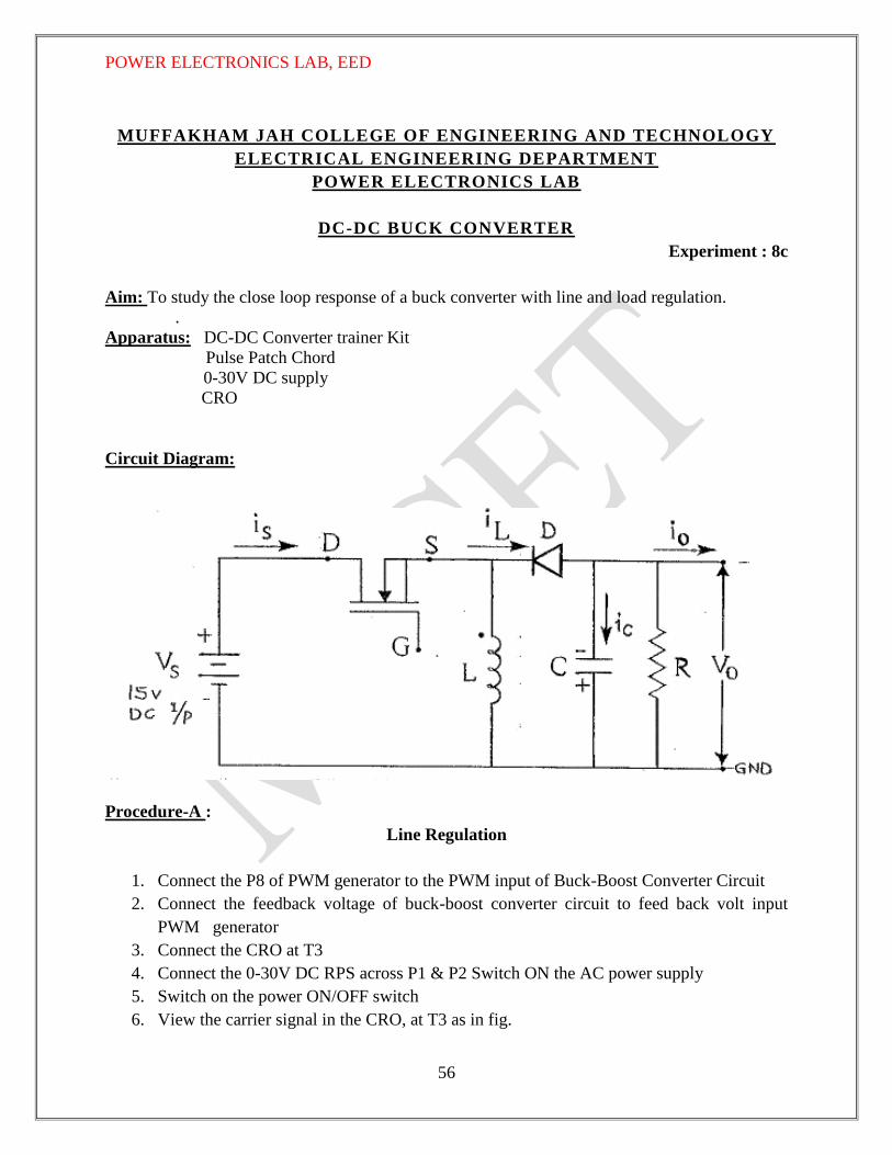
DC-DC BUCK CONVERTER
Experiment : 8c
Aim: To study the close loop response of a buck converter with line and load regulation.
.
Apparatus: DC-DC Converter trainer Kit
Pulse Patch Chord
0-30V DC supply
CRO
Circuit Diagram:
Procedure-A :
Line Regulation
1. Connect the P8 of PWM generator to the PWM input of Buck-Boost Converter Circuit
2. Connect the feedback voltage of buck-boost converter circuit to feed back volt input
PWM generator
3. Connect the CRO at T3
4. Connect the 0-30V DC RPS across P1 & P2 Switch ON the AC power supply
5. Switch on the power ON/OFF switch
6. View the carrier signal in the CRO, at T3 as in fig.

POWER ELECTRONICS LAB, EED
57
7. Set the switch SW1 in upward position, SW2 in downward direction and view the PWM
signal at T1 as in fig. The duty cycle may be changed by changing the SET VOLTAGE.
8. Note down Ton and Toff values to calculate the duty cycle (D = Ton/T) .
9. Switch ON the DC 15V supply
10. View the following wave forms
a. Device Current IQ across I1 & I2
b. Diode current ID across I3 & I4
c. Inductor Current IL across I3 & I7
d. Device Voltage VQ across I2 & I3
e. Rectified Voltage across I5 & I8
f. Inductor voltage VL across I7 & I8
g. The feed back signal at T6
11. Connect the CRO across P5 & P6 to view the output voltage and calculate the output
voltage using the formula V0 = [D] * Vs
12. Vary the input voltage from 0 to 15V.
Observations:
Line Regulation
Measure and tabulate the following readings.
SET voltage = below 15 V
Note: Buck operation not possible for maximum set voltage of the pulses ie.4.7 V
Set pulse voltage: minimum (1.2)V
S.no Input Voltage
Vin
TON TOFF D= TON/T Output
Voltage
Measured(Vo)
Output calculated
Vo= [D]*Vs
Set voltage: 2.7V (50% 0f pulse voltage)
S.no Input Voltage
Vin
TON TOFF D= TON/T Output
Voltage
Measured(Vo)
Output calculated
Vo= [D]*Vs

POWER ELECTRONICS LAB, EED
58
Procedure-B :
Load Regulation
1. Connect the rheostat bet P5 and P6
2. Connect an ammeter in series with the rheostat
3. For 0 external resistance the output is 5V, (IL=.3-.7Amp)
4. vary the resistance till the load current is 0.7Amp
5. Tabulate the measured readings
Observations:
Load Regulation
Measure and tabulate the following readings.
Vary the rheostat for (IL = 0.3 to 0.7Amps)
SET Input voltage = 15V
Set pulse voltage: minimum (1.2V) (Buck operation )
Input
Voltage
Vin
TON TOFF D= TON/T
(T= TON+
TOFF)
Load
Resistor
(R Ω)
IL(amps) Output Voltage
Measured(Vo)
Output calculated
Vo= I*R(volts)
15V
Expected Waveforms For Line And Load Regulation:

POWER ELECTRONICS LAB, EED
59
Results:
Line Regulation
The close loop response for buck converter for line regulation has been examined
The output Voltage is maintained at _______________ Volts with an input voltage from ----------------Volt
to --------------- Volt
Load Regulation
The close loop response of buck converter with load regulation has been examined.
Discussion of Result:
Compare the theoretical results with practical results.
Effect of change in duty cycle on output voltage for line & load regulation.

POWER ELECTRONICS LAB, EED
60
MUFFAKHAM JAH COLLEGE OF ENGINEERING AND TECHNOLOGY
ELECTRICAL ENGINEERING DEPARTMENT
POWER ELECTRONICS LAB
THREE PHASE BRIDGE RECTIFIERS
Experiment: 9
Aim: To verify and measure output voltage of half control and full control of a three
phase bridge rectifiers
Apparatus: Three Phase bridge rectifier trainer Kit
CRO, DC Voltmeter
Patch chords
Theory: Phase control thyristors can control the output voltage of a rectifier, by varying
the firing angle or delay angle α of the thyristor. In phase control thyristor
commutation or turning OFF takes place by line or natural commutation. It has
applications in industrial variable speed drives from very low to very high power
levels as high as few Mega watts.
Circuit Diagram:
Half controlled Rectifier
V1
120 Vrms
50 Hz
0Deg
D1D2
R1
D4 D5
D6
D3
D7
V5
120 Vrms
50 Hz
0Deg V6
120 Vrms
50 Hz
0Deg
3Ph
Star AC
supply,
50 Hz

POWER ELECTRONICS LAB, EED
61
Procedure:
Full wave Half controlled rectifier
1. Connect RL1 from load panel across load
2. Connect R-R1 , Y-Y1 & B-B1 and also R-R3 , Y-Y3 & B-B3
3. Connect load between Positive terminal of DC supply and negative terminal of DC
supply
4. Connect the oscilloscope through attenuator across the load and switch on the power.
5. Observe the Load voltage and Phase diode voltage waveforms
6. Turn the phase control clockwise ie. Firing angle”α”and calculate load voltage VL
7. Repeat for various loads and observe the change in the waveforms
Observation Table:
Vrms
(line)
Vm (line) T(msec) t (msec) α (degrees) Vo(measured) Vo(calculated)
48.1
68.01
3.4
0.4
14.11
62.2
63.97
Model Calculation:
Vm = Vrms*√2
α = (t/T)*120
= (0.4/3.4)*120
= 14.11
Vo (calculated) = 3Vm (line )
2п (1+cosα) V
= 3∗48.1∗√2
2п (1+cos14.11
)
Vo = 63.97V

POWER ELECTRONICS LAB, EED
62
Expected graphs:
Half controlled
POWER ELECTRONICS LAB, EED
63

POWER ELECTRONICS LAB, EED
64
Results: The output waveforms across the load have been observed for half controlled 3
phase rectifier
Discussion of Result:
Compare the theoretical and practical values of output voltage and analyse the output
voltage waveform for different firing angles.
Comment on conduction period of each thyristor .

POWER ELECTRONICS LAB, EED
65
MUFFAKHAM JAH COLLEGE OF ENGINEERING AND TECHNOLOGY
ELECTRICAL ENGINEERING DEPARTMENT
POWER ELECTRONICS LAB
SINGLE PHASE SEMI CONVERTER (FULL CONTROLLED)
Experiment: 10a
Aim: To Study the single phase half wave rectifier (full controlled) with R RL and RLE loads
using Multisim Simulation Software
Apparatus: Multisim simulation software
Theory: A single phase half wave circuit is one which produces only one pulse of load current
during one cycle of source voltage. A simple controlled rectifier circuit consists of a
thyristor connected to a source and a load. The SCR conducts only when the anode
current is more positive than the cathode and a gating signal is applied. It blocks the
current until it is triggered. It turns OFF by reversal of voltage at ωt = π.3π, 5π etc. since
it reverse biases the device.
Firing angle is defined as the angle between the instant the thyristor conducts if it were
a diode and the instant it is triggered.
Procedure: Switch ON the computer double click on the multisim icon. You get the drawing
window. Pick the components from the virtual component library.ON the grid. Rig
the circuit for the R, RL and RLE loads .Pick the CRO from the instrument bar
and connect it across the load also pick and drop the multimeter across the load.
Connect a square wave source between the gate and the anode of the SCR as
firing pulse and Observe the wave forms.
Circuit Diagram:
R-Load
V1
120 Vrms
50 Hz
0Deg
XSC1
A B
G
T
R1
500Ω
D1
2N1599
V2
0 V 10 V
10msec 20msec

POWER ELECTRONICS LAB, EED
66
RL-Load
RLE- Load
Expected Waveforms:
R-LOAD
V1
120 Vrms
50 Hz
0Deg
XSC1
A B
G
T
R1
500Ω
D1
2N1599
V2
0 V 10 V
10msec 20msec
L1
500mH
V1
120 Vrms
50 Hz
0Deg
XSC1
A B
G
T
R1
500Ω
D1
2N1599
V2
0 V 10 V
10msec 20msec
L1
500mH
V3
60 V

POWER ELECTRONICS LAB, EED
67
RL LOAD
RLE LOAD

POWER ELECTRONICS LAB, EED
68
Simulation Results Of Output Voltage:
Semi Converter with R-Load
Semi Converter with RL-Load

POWER ELECTRONICS LAB, EED
69
Semi Converter with RLE-Load
Results: The multisim software is learnt. The wave forms for single, phase half wave R Rl and
RLE loads have been observed.
Discussion of Result:
Comment on changes in output voltage waveform with change in firing angle.
Comment on changes in output voltage waveform with change in load.

POWER ELECTRONICS LAB, EED
70
MUFFAKHAM JAH COLLEGE OF ENGINEERING AND TECHNOLOGY
ELECTRICAL ENGINEERING DEPARTMENT
POWER ELECTRONICS LAB
SINGLE PHASE FULL CONVERTER (FULL CONTROLLED)
Experiment:10b
Aim: To Study the single phase full wave rectifier (full controlled) with R RL and RLE loads
using Multisim Simulation Software
Apparatus: Multisim simulation software
Theory: A single phase half wave circuit is one which produces only one pulse of load current
during positive half cycle of source voltage and another pulse of load current in
negative half cycle of source voltage, both in same direction. Hence producing DC
voltage for an applied Ac voltage. A Full bridge half controlled rectifier circuit
consists of a 2-thyristors and two diodes connected to a source and a load whereas a
Full bridge full controlled rectifier circuit consists of a 4-thyristors connected to a
source and a load. The SCR conducts only when the anode current is more positive
than the cathode and a gating signal is applied. It blocks the current until it is
triggered. It turns OFF by reversal of voltage at ωt = π. 3π, 5π etc. since it reverse
biases the device.
Firing angle is defined as the angle between the instant the thyristor conducts if it
were a diode and the instant it is triggered.
Procedure:
Switch ON the computer double click on the multisim icon. You get the drawing window.
Pick the components from the virtual component library.ON the grid. Rig the circuit for the R,
RL, RL with Freewheeling Diode and RLE loads .Pick the CRO from the instrument bar and
connect it across the load also pick and drop the multimeter across the load. Connect a square
wave source between the gate and the anode as firing pulse of the SCR and Observe the wave
forms.

POWER ELECTRONICS LAB, EED
71
Circuit Diagram :
Full Converter half controlled with R-Load:
Full Converter half controlled with RL-Load:
V1
120 Vrms
50 Hz
0Deg
D1D2
R1
XSC1
A B
G
T
D4 D5
V3
V4
D6
V1
240 Vrms
50 Hz
0Deg
R1
XSC1
A B
G
T
D4 D5
L1
50mH
IC=0A
D2
2N1599D1
2N1599

POWER ELECTRONICS LAB, EED
72
Expected Waveform of Output Voltage:
V1
240 Vrms
50 Hz
0Deg
R1
XSC1
A B
G
T
D4 D5
L1
50mH
IC=0A
D2
2N1599D1
2N1599
D3
DIODE_VIRTUAL
V1
240 Vrms
50 Hz
0Deg
R1
XSC1
A B
G
T
D4 D5
L1
50mH
IC=0A
D2
2N1599D1
2N1599
V2
120 V

POWER ELECTRONICS LAB, EED
73
For Full & half controlled Converter with R-Load (𝛂 = 𝟑𝟎°)
Full & half controlled Converter with R-Load (𝛂 = 𝟔𝟎°)
Full & half controlled Converter with RL-Load

POWER ELECTRONICS LAB, EED
74
Full controlled Converter with RL-Load & Freewheeling Diode
Full controlled Converter with RLE-Load
Results: The multisim software is learnt. The wave forms for single phase half wave with R RL
and RLE loads have been observed.
Discussion of Result:
Comment on changes in output voltage waveform with change in firing angle.
Comment on changes in output voltage waveform with change in load.

POWER ELECTRONICS LAB, EED
75
MUFFAKHAM JAH COLLEGE OF ENGINEERING AND TECHNOLOGY
ELECTRICAL ENGINEERING DEPARTMENT
POWER ELECTRONICS LAB
THREE PHASE INVERTER
Experiment: 11
Aim: To Study the operation of 3- phase inverter 180 & 120
mode of operation and observe
the output waveforms using Multisim software.
Apparatus: Multisim software.
Theory:
Inverter basically converts DC to AC. In three phase inverter the output is three phase
ac. It works in two modes depending upon the conduction period of each transistor in the circuit
ie.180& 120
.In both the modes each transistor is triggered in the same sequence as they are
numbered with an interval of 60.In complete one cycle of output there exists six steps of
operation each of duration 60.In every step of 60
duration in 180
mode of operation, three
switches are conducting two from upper group and one from lower group & in 120 mode of
operation, one switch from upper group and one from lower group conducts.
Procedure:
Switch ON the computer, double click on the multisim icon. You get the drawing
window. Pick the components from the virtual component library. ON the grid, rig the circuit for
the 3-phase inverter circuit with R-load. Connect a square wave source between the gate and the
anode of all six transistors. Pick the CRO from the instrument bar and connect it across the load
Observe the output wave forms for 180& 120
(line & phase voltages)
modes of operation.
Instead of thyristors, transistors are used as switches in order to avoid the complexity of the
circuit as use of thyristors will add the commutation circuit input being DC
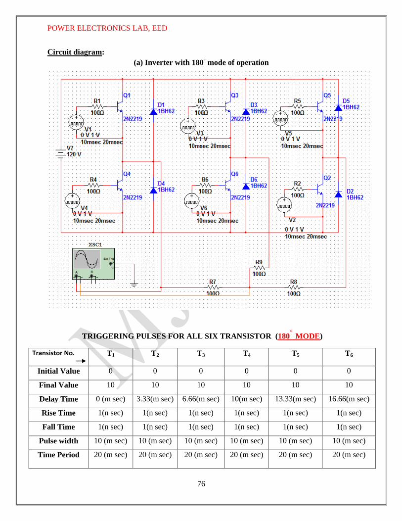
POWER ELECTRONICS LAB, EED
76
Circuit diagram:
(a) Inverter with 180 mode of operation
TRIGGERING PULSES FOR ALL SIX TRANSISTOR (180 MODE)
Transistor No. T1 T2 T3 T4 T5 T6
Initial Value 0 0 0 0 0 0
Final Value 10 10 10 10 10 10
Delay Time 0 (m sec) 3.33(m sec) 6.66(m sec) 10(m sec) 13.33(m sec) 16.66(m sec)
Rise Time 1(n sec) 1(n sec) 1(n sec) 1(n sec) 1(n sec) 1(n sec)
Fall Time 1(n sec) 1(n sec) 1(n sec) 1(n sec) 1(n sec) 1(n sec)
Pulse width 10 (m sec) 10 (m sec) 10 (m sec) 10 (m sec) 10 (m sec) 10 (m sec)
Time Period 20 (m sec) 20 (m sec) 20 (m sec) 20 (m sec) 20 (m sec) 20 (m sec)

POWER ELECTRONICS LAB, EED
77
Circuit diagram: (b) Inverter with 120 mode of operation
TRIGGERING PULSES FOR ALL SIX sTRANSISTORS (120 MODE)
Transistor No. T1 T2 T3 T4 T5 T6
Initial Value 0 0 0 0 0 0
Final Value 10 10 10 10 10 10
Delay Time 0 (m sec) 3.33(m sec) 6.66(m sec) 10(m sec) 13.33(m sec) 16.66(m sec)
Rise Time 1(n sec) 1(n sec) 1(n sec) 1(n sec) 1(n sec) 1(n sec)
Fall Time 1(n sec) 1(n sec) 1(n sec) 1(n sec) 1(n sec) 1(n sec)
Pulse width 6.66(m sec) 6.66(m sec) 6.66(m sec) 6.66(m sec) 6.66(m sec) 6.66(m sec)
Time Period 20 (m sec) 20 (m sec) 20 (m sec) 20 (m sec) 20 (m sec) 20 (m sec)

POWER ELECTRONICS LAB, EED
78
Expected Graphs: (a) Inverter with 180 mode of operation

POWER ELECTRONICS LAB, EED
79
Expected Graphs:
(b) Inverter with 120 mode of operation
POWER ELECTRONICS LAB, EED
80
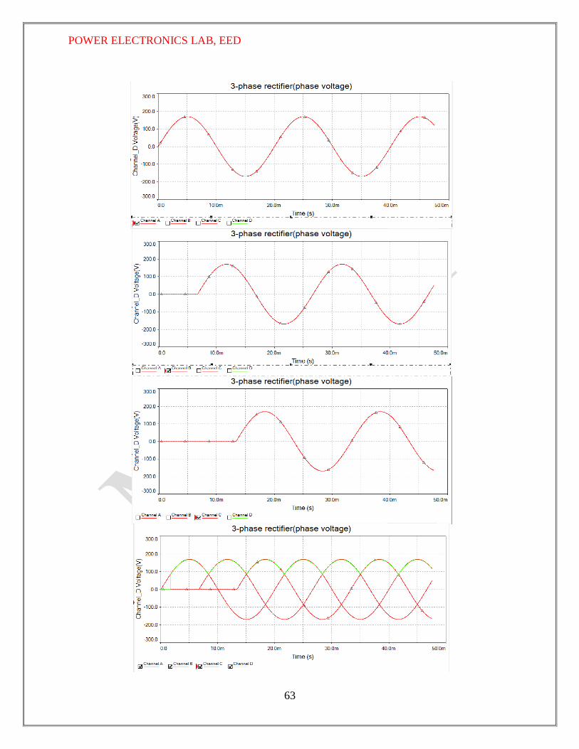
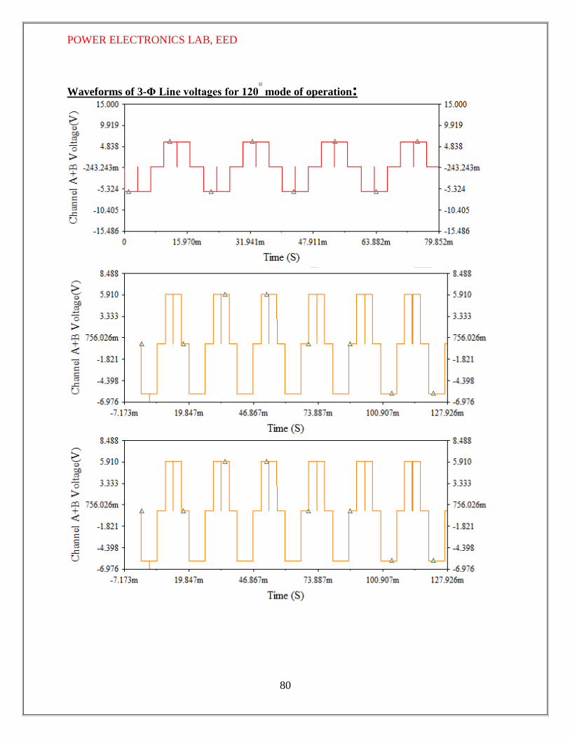
Waveforms of 3-Φ Line voltages for 120
mode of operation:

POWER ELECTRONICS LAB, EED
81
Waveforms of 3-Φ Line voltages for 180
mode of operation:

POWER ELECTRONICS LAB, EED
82
Result: The multisim software is learnt and the waveforms of three phase inverter with R-Load
(phase & line voltages) are observed for both180 & 120
modes of operation.
Discussion of Result:
Analyze the output voltage (line & phase) waveforms for both180
& 120 modes of
operation and comment on the result.

POWER ELECTRONICS LAB, EED
83
MUFFAKHAM JAH COLLEGE OF ENGINEERING AND TECHNOLOGY
ELECTRICAL ENGINEERING DEPARTMENT
POWER ELECTRONICS LAB
SIMULATION OF SINGLE PHASE CYCLOCONVERTER
Experiment: 12
Aim: To Study the operation of Cycloconverter and observe the output waveforms using
Multisim software.
Apparatus: Multisim software
Theory:
In cycloconverter one group of thyristors produce positive polarity of the load
voltage and other group produces the negative polarity of the load voltage. Only one of them will
conduct at a time. When ‘P’ is positive with respect to ‘O’, then SCR1 will conduct otherwise
SCR2 will conduct. Thus in both the half cycles of the input, the load voltage will be positive.
The SCR’s get turned off by natural commutation at the end of every half cycle.
Depending on the desired frequency gating pulses to positive group of SCR’s (T1, T2) &
negative group of SCR’s (T3, T4) are given.
Procedure:
Switch ON the computer, double click on the multisim icon. You get the drawing
window. Pick the components from the virtual component library. ON the grid, rig the circuit for
the cycloconverter circuit with R-load. Connect a pulse voltage by selecting a signal voltage
source from the virtual component between the gate and the cathode of all thyristors. Pick the
CRO from the instrument bar and connect it across the load. Observe the output wave forms for
f, f/2, f/3, f/4 modes of operation as per their respective circuits and triggering pulse sequences..
TRIGGERING PULSES FOR “F “MODE OF OPERATION
SCR No. T1 T2 T3 T4
Initial Value 0 0 0 0
Final Value 10 10 10 10
Delay Time 0 (m sec) 0(m sec) 10(m sec) 10(m sec)
Rise Time 1(n sec) 1(n sec) 1(n sec) 1(n sec)
Fall Time 1(n sec) 1(n sec) 1(n sec) 1(n sec)
Pulse width 10 (m sec) 10 (m sec) 10 (m sec) 10 (m sec)
Time Period 20 (m sec) 20 (m sec) 20 (m sec) 20 (m sec)
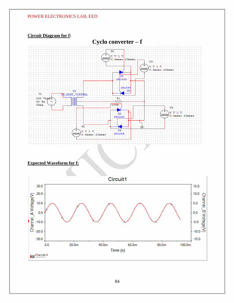
POWER ELECTRONICS LAB, EED
84
Circuit Diagram for f:
Cyclo converter – f
Expected Waveform for f:

POWER ELECTRONICS LAB, EED
85
TRIGGERING PULSES FOR “F/2 “MODE OF OPERATION
SCR No. T1 T2 T3 T4
Initial Value 0 0 0 0
Final Value 10 10 10 10
Delay Time 0 (m sec) 10(m sec) 30(m sec) 20(m sec)
Rise Time 1(n sec) 1(n sec) 1(n sec) 1(n sec)
Fall Time 1(n sec) 1(n sec) 1(n sec) 1(n sec)
Pulse width 10 (m sec) 10 (m sec) 10 (m sec) 10 (m sec)
Time Period 40 (m sec) 40 (m sec) 40 (m sec) 40 (m sec)
Circuit Diagram for f/2: Cyclo converter - f/2

POWER ELECTRONICS LAB, EED
86
Expected Waveform for f/2:
TRIGGERING PULSES FOR “F/3“MODE OF OPERATION
SCR No. T1 T1 T2 T3 T3 T4
Initial Value 0 0 0 0 0 0
Final Value 10 10 10 10 10 10
Delay Time 0 (m sec) 20 (m sec) 10(m sec) 30(m sec) 50(m sec) 40(m sec)
Rise Time 1(n sec) 1(n sec) 1(n sec) 1(n sec) 1(n sec) 1(n sec)
Fall Time 1(n sec) 1(n sec) 1(n sec) 1(n sec) 1(n sec) 1(n sec)
Pulse width 10 (m sec) 10 (m sec) 10 (m sec) 10 (m sec) 10 (m sec) 10 (m sec)
Time Period 60 (m sec) 60 (m sec) 60 (m sec) 60 (m sec) 60 (m sec) 60 (m sec)

POWER ELECTRONICS LAB, EED
87
Circuit Diagram for f/3:
Cyclo converter - f/3
Expected Waveform for f/3:

POWER ELECTRONICS LAB, EED
88
TRIGGERING PULSES FOR “F/4“MODE OF OPERATION
SCR No. T1 T1 T2 T2 T3 T3 T4 T4
Initial
Value 0 0 0 0 0 0 0 0
Final
Value 10 10 10 10 10 10 10 10
Delay
Time 0 (m sec) 20(msec) 10(msec) 30(msec) 50(msec) 70(msec) 40(m sec) 60(m sec)
Rise
Time 1(n sec) 1(n sec) 1(n sec) 1(n sec) 1(n sec) 1(n sec) 1(n sec) 1(n sec)
Fall
Time 1(n sec) 1(n sec) 1(n sec) 1(n sec) 1(n sec) 1(n sec) 1(n sec) 1(n sec)
Pulse
width 10 (msec) 10(msec) 10(msec) 10(msec) 10(msec) 10(msec) 10 (m sec) 10 (m sec)
Time
Period 80 (msec) 80(msec) 80(msec) 80(msec) 80(msec) 80(msec) 80 (m sec) 80 (m sec)

POWER ELECTRONICS LAB, EED
89
Circuit Diagram for f/4:
Cyclo converter - f/4
Expected Waveform for f/4:

POWER ELECTRONICS LAB, EED
90
Result: The multisim software is learnt and the waveforms of Cycloconverter with R-Load are
observed for f, f/2, f/3, f/4 modes of operation.
Discussion of Result:
Comment on Time Period and frequency with reference to input frequency for different
levels of output frequency.

POWER ELECTRONICS LAB, EED
91

POWER ELECTRONICS LAB, EED
92
VIVA QUESTIONS
V-I CHARACTERISTICS OF SCR
1. What is a Thyristor?
Ans) Thyristor is derived from the properties of a Thyratron tube and a Transistor. It is used as
another name for SCR’S. They are power Semiconductor devices used for power control
applications.
2. What are SCR’s?
SCR’s is Silicon controlled Rectifiers. They are basically used as Rectifiers
3. Draw the structure of an SCR?
4. What are the different methods of turning on an SCR?
*Anode to cathode voltage is greater than break over voltage.
*Gate triggering *When dv/dt exceeds permissible value.
*Gate cathode junction is exposed to light.
5. What is Forward break over voltage?
The voltage Vak at which the SCR starts conducting is called as Forward Break over voltage
Vbo. This happens when the junction J2 undergoes Avalanche breakdown due to high reverse
bias on junction J2.
6. What is Reverse break over voltage?
If the reverse voltage is increased more than a critical value, avalanche Breakdown will occur at
J1 and J3 increasing the current sharply. This is Reverse break over voltage VBO.
7. Why is Vbo greater than VBR?
In SCR the inner two p-n regions are lightly doped due to which the thickness of the depletion
region at junction J2 is higher during forward bias than that of J1 and J3 under reverse bias.
8. What are modes of working of an SCR?
Reverse blocking mode, Forward blocking mode and Forward conduction mode are the modes of
working of an SCR.
9. Draw the V-I characteristics of SCR.
Ans) Refer figure 1.1(a)

POWER ELECTRONICS LAB, EED
93
10. Why does high power dissipation occur in reverse blocking mode?
High power dissipation occurs because as voltage increases beyond Vbr current increases
rapidly.
11. Why shouldn’t positive gate signal be applied during reverse blocking Mode?
If we apply positive gate signal J3 becomes forward biased. Reverse leakage current increases
and Thyristor gets damaged due to large power dissipation.
12. Explain reverse current Ire?
When cathode voltage is positive, J2 is forward biased; J1 and J3 are reverse biased. The
thyristors will be in reverse blocking state and reverse leakage current Ire flows.
13. What happens when gate drive is applied?
When gate drive is applied avalanche breakdown occurs at J2 causing excessive flow of charges
and hence current surge. This turns the SCR into conduction state faster i.e. the Thyristor turns
on at lower and lower anode to cathode voltages, which are less than Vbo.
14. Differentiate between holding and latching currents?
Holding current is the minimum amount of current below, which SCR does not conduct. It
is associated with the presence of gate terminal and concerns turn off condition.
Latching current is the minimum amount of current required for the SCR to conduct. It is
associated with absence of gate terminal and concerns turn on process. It is greater than holding
current.
15. Why is dv/dt technique not used?
As this causes false triggering even when gate or voltage Vak is not applied, dv/dt technique is
not used. Snubbed circuit, which is combination of a C, avoids this and R .The capacitor is
placed in parallel with SCR.
16. What sided?
At the time of turn on, anode current increases rapidly. This rapid variation is not spread across
the junction area of the thyristors. This creates local hotspots in the junction and increases the
junction temperature and hence device may be damaged. This is avoided by connecting an
inductor in series with an SCR.
17. Why should the gate signal be removed after turn on?
This prevents power loss in the gate junction.
18. Is a gate signal required when reverse biased?
No, otherwise SCR may fail due to high leakage current.

POWER ELECTRONICS LAB, EED
94
19. What are different types of firing circuits to trigger SCR?
*R firing circuit.
*RC firing circuit.
*UJT firing circuit.
*Digital firing circuit.
20. What type of triggering is used in SCR?
Pulse triggering.
21. What is offset current?
When anode voltage is made positive, J1 and J3 are forward biased, J2 is reverse biased. The
Thyristor is in forward blocking or off state condition and the leakage current is known as
offset current Io.
22. What are the advantages of SCR?
*Very small amount of gate drive is required since SCR is regenerative device.
*SCR’s with high voltage and current ratings are available.
*On state losses are reduced.
23. What are the disadvantages of SCR’s?
*Gate has no control once the SCR is turned on.
*External circuits are required to turn off the SCR.
*Operating frequencies are very low.
*Snubber (RC circuits) is required for dv/dt protection.
24. What are applications of SCR?
*SCR’s are best suitable for controlled rectifiers.
*AC regulators, lighting and heating applications.
*DC motor drives, large power supplies and electronic circuit breakers.
25. What is the difference between an IGBT and SCR?
IGBT comprises of a BJT and a MOSFET where as an SCR comprises of two BJT’s.
26. Can we replace a SCR by a microprocessor by writing a program to exhibit
characteristics of SCR?
No, we can verify or test the working of SCR using microprocessor but we cannot replace
it practically.
__________________________________*********___________________________________
____

POWER ELECTRONICS LAB, EED
95
CHARACTERISTICS OF MOSFET
1. What are MOSFET’s?
Metal oxide silicon di-oxide field effect transistor is a voltage-controlled device. The
parts of MOSFET are gate, drain and source.
2. Draw the symbol of MOSFET.
3. What is the difference between MOSFET and BJT?
The MOSFET is a voltage controlled device where as BJT is a current controlled device.
4. What is the difference between JFET and MOSFET?
There is no direct contact between the gate terminal and the n-type channel of
MOSFET.
5.Draw the structure of MOSFET?
6.What are the two types of MOSFET?
*Depletion MOSFET - N channel in p substrate. -P channel in n substrate. *Enhancement
mosfet –virtual n channel in p substrate -Virtual p channel in n substrate.
7. What is the difference between depletion and enhancement MOSFET?
The channel in the centre is absent for enhancement type MOSFET but the channel is
present in depletion type MOSFET. The gate voltage can either be positive or negative in
depletion type MOSFET’s but enhancement MOSFET responds only for positive gate
voltage.
8. How does n-drift region affect MOSFET?

POWER ELECTRONICS LAB, EED
96
The n- drift region increases the onstage drop of MOSFET and also the thickness of this region
determines the breakdown voltage of MOSFET.
9. How are MOSFET’s suitable for low power high frequency applications?
MOSFET’s have high on state resistances due to which losses increase with the increase in the
power levels. Their switching time is low and hence suitable for low power high frequency
applications.
10. What are the requirements of gate drive in MOSFET?
*The gate to source input capacitance should be charged quickly. *MOSFET turns on when gate
source input capacitance is charged to sufficient level. *The negative current should be high to
turn off MOSFET.
11. Draw the switching model of MOSFET.
12. What is rise time and fall time?
The capacitor Cgs charges from threshold voltage to full gate voltage Vgsp. The time required
for this charging is called rise time. During this period, drain current rises to full value. The
capacitor Cgs keeps on discharging and its voltage becomes equal to threshold voltage Vt.The
time required for this discharge Cgs from Vgsp to Vt is called fall time.
13. What is pinch off voltage?
The voltage across gate to source at which the drain to source current becomes zero is called
pinch off voltage.
14. In which region does the MOSFET used as a switch?
In the linear region.
15. Which parameter defines the transfer characteristics?
The Tran conductance Gm=Id/Vgs .
16. Why are MOSFET’s mainly used for low power applications?
MOSFET’s have high on state resistance Rds. Hence for higher currents; losses in the
MOSFET’s are substantially increased. Hence MOSFET’s are substantially increased. Hence,
MOSFET’s are mainly used for low power applications.
17.How is MOSFET turned off?
To turn off the MOSFET quickly, the negative gate current should be sufficiently high to
discharge gate source input capacitance.

POWER ELECTRONICS LAB, EED
97
18. What are the advantages of vertical structure of MOSFET?
*On state resistance of MOSFET is reduced.
*Width of the gate is maximized.
Hence, gain of the device is increased.
19. What are the merits of MOSFET?
* MOSFET’s are majority carrier devices.
*MOSFET’s have positive temperature coefficient, hence their paralleling is easy.
*MOSFET’s have very simple drive circuits.
*MOSFET’s have short turn on and turn off times; hence they operate at high frequencies.
*MOSFET’s do not require commutation techniques.
*Gate has full control over the operation of MOSFET.
20. What are demerits of MOSFET?
*On state losses in MOSFET are high.
*MOSFET’s are used only for low power applications.
*MOSFET’s suffer from static charge.
21. What are the applications of MOSFET?
*High frequency and low power inverters.
*High frequency SMPS.
*High frequency inverters and choppers.
*Low power AC and DC drives.
__________________________________*********___________________________________
____
CHARACTERISTICS OF IGBT
1. What is IGBT?
Insulated gate bipolar transistor is the latest device in power Electronics .It is obtained by
combining the properties of BJT and MOSFET.
2. In what way IGBT is more advantageous than BJT and MOSFET?
*It has high input impedance of the MOSFET and has low on-state voltage drop.
*The turn off time of an IGBT is greater than that of MOSFET.
*It has low onstage conduction losses and there is no problem of second Breakdown as in case of
BJT.
*It is inherently faster than a BJT.
3.Draw the symbol of IGBT.

POWER ELECTRONICS LAB, EED
98
4. Draw the equivalent circuit of IGBT.
5. What are on state conduction losses? How is it low in IGBT?
A high current is required to break the junctions in BJT. This results in On state conduction
losses. The conduction losses in IGBT are proportional To duty cycle of the applied voltage. By
reducing the duty cycle conduction losses can be reduced.
6. What is second breakdown phenomenon?
As the collector voltage drops in BJT there is an increase in collector Current and this
substantially increase the power dissipation. This Dissipation is not uniformly spread over the
entire volume of the device but is concentrated in highly localized regions where the local
temperature may grow and forms the black spots. This causes the destruction of BJT. This is
second breakdown.
7. What is switching speed?
The time taken to turn on or turn off a power device is called switching Speed.
8. Can we observe the transfer and collector characteristics of IGBT on CRO?
No. Because the waveform which is to be observed on the CRO should vary with respect to time
otherwise we can see only a straight line on the CRO.
9. What are merits of IGBT?
*The drive is simple.
*Onstage losses are reduced.
*No commutation circuits are required.
*Gate has full control.
*Switching frequencies are higher.
*It has flat temperature coefficient.
10. What are demerits of IGBT?
*They have static charge problems.
*They are very costly.
11. What are the applications of IGBT’s?

POWER ELECTRONICS LAB, EED
99
*Ac motor drives. (Inverters)
*Dc to Dc power supplies. (Choppers)
*UPS systems.
*Harmonic compensators.
12. Why is silicon used in all power semiconductor devices and why not? Germanium?
The leakage current in silicon is very small compared to germanium. The germanium is also
more sensitive compared to silicon.
13. What is pinch off voltage?
When Vge is made negative, electrons in the n-channel get repelled Creating a depletion region
resulting in a narrower effective channel. If Vge is made negative enough so as to completely
eliminate the channel (High resistance, low current state), that value is called the pinch off
Voltage.
14. What is threshold voltage?
Threshold voltage is the voltage Vge at which IGBT begins to conduct.
15. How is IGBT turned off?
An IGBT can turn off by discharging the gate by means of short circuiting it to the emitter
terminal.
16. What is the rating of IGBT?
The current rating can be up to 400A, 1200V with switching frequency of 20 KHz.
__________________________________*********___________________________________
____
Controlled HWR &FWR using R & RC Triggering circuit
1. What is the maximum firing angle of R-triggering circuit and why?
The maximum firing angle is 90°. This is because the source voltage reaches maximum
value of 90° point and the gate current has to reach Ig(min) some where between 0-90°.
This limitation means that load voltage waveform can only be varied from α = 0° to α =
90°.
2. What are the disadvantages of R triggering?
• Trigger angle α is greatly dependent on the SCR’s Ig(min) and this value varies between
SCR’s and it is also temperature dependent.
• Maximum triggering angle achievable is 90°.

POWER ELECTRONICS LAB, EED
100
3. In R-triggering circuit why is Rmin is connected in series with variable resistor?
The limiting resistor Rmin is placed between anode and gate so that the peak gate current
of the thyristor Igm is not exceeded.
4. What is the maximum firing angle of RC-triggering and why?
Maximum firing angle is 180°. This is because capacitor voltage and AC line voltage
differ in phase. By adjusting the value of R it is possible to vary the delay in turning on
the SCR from 0 to 10 msec and hence vary the firing angle from 0° to 180°.
__________________________________*********___________________________________
____
UJT firing circuit for HWR and FWR circuits.
1. What is an UJT and draw its equivalent circuit?
UJT-uni junction transistor. It has only one type of charge carriers. It has three terminals emitter,
base 1 and base 2. (‘Duo base’ as it has 2 bases)
2. Why is an UJT used in SCR firing circuit?
The voltage at base 1 of UJT is smaller than the voltage needed to trigger the Scrim the voltage
is high, then it will trigger the SCR as soon as the ac supply is on.
3. Why is the isolation needed between Thyristor and firing circuit?
The trigger circuit operates at low power levels (5-20 volts) whereas thyristors operate at high
voltage levels (250 volts). Hence if the Thyristor acts as a short the entire 250volts get applied
across the firing circuit causing damage. Hence isolation is needed.
4. How is a pulse transformer different from other transformer?
A pulse transformer is one in which the input at the primary is current which is transformed into
a pulse at the secondary. Thus it does not step-up and step-down as other transformers.
5. What are the features of pulse transformer?
The primary magnetizing inductance is high, coupling efficiency is high, and interwinding
capacitance is low and has greater insulation.
6. What are the advantages of using pulse transformer?
*Multiple secondary windings allow simultaneous gating signals to series and parallel connected
thyristors. *Control circuit and power circuit can be isolated.
7. Why i s UJT used in SCR firing circuit?

POWER ELECTRONICS LAB, EED
101
As the UJT works in a mode called as a relaxation oscillator i.e. UJT turns on or off depending
on the charging and discharging of the capacitor. Time constant can be varied with Chance delay
angle can be varied .The UJT thus gives a firing angle range of 0- 180.Vz is supply to UJT, the
discharging current when passed through the pulse transformer triggers SCR with pulses.
8. Why is the zeenar diode used?
The zeenar diode provides a constant supply voltage for UJT. It enables synchronization with
zero crossings. Zeenar diode acts as a regulator. The zeenar clamps the rectified voltage to vs. to
prevent erratic firing. This sneer voltage acts as a supply for UJT relaxation oscillator.
9. What is meant by ramp control, open loop control or manual control with respect to UJT
firing circuit?
Ramp control-The graph of time period in milliseconds with the firing angle in degrees is a
ramp. The ramp slope can be controlled by the potentiometer. Manual control-The potentiometer
in the kit can be used to get various firing angles. This is manual control.
10. What is a firing circuit?
It is a circuit, which is used to trigger a device at various instants of time.
11. Why a bridge rectifier is used?
The bridge rectifier gives a full wave rectified output, which is high in efficiency and least ripple
factor.
12. What is the load used?
Load is high power dissipation resistor.
13. What is time constant of a circuit?
Time constant of a circuit=RC where R=resistance C=capacitance It gives the time of charging
and discharging of a capacitor.
14. What are the merits of UJT firing circuit over RC triggering circuit?
* Firing angle remains stable.
*Advantages of pulse transformer.
15. What are the advantages of UJT pulse trigger circuit?
The resistors, capacitors depend heavily on the trigger characteristics of the Thyristor used. The
power dissipation is high due to prolonged pulse. But the pulse triggering can accommodate
wide tolerances in triggering characteristics by instantaneously overdriving the gate. The power
level in such circuits is lower as the triggering energy can be stored slowly and discharged
rapidly when the triggering is required.

POWER ELECTRONICS LAB, EED
102
16. Why is UJT used as relaxation oscillator?
The UJT is used as a relaxation oscillator to obtain sharp, repetitive pulses with good rise time.
Also it has good frequency stability against variation in the supply voltage and temperature.
17. What are the applications of UJT trigger circuits?
*Used to trigger SCR’s in single-phase converters, single-phase ac regulators.
*Used in oscillators
*Used in timing circuits
18. What is valley voltage?
It is the voltage at which the UJT turns off and the capacitor starts charging again.
19. What is the discharging path if the capacitor?
The capacitor discharges through emitter, base and primary of the pulse transformer.
20. What is relaxation oscillator?
When the capacitor discharges to a valley voltage, the UJT turns off and capacitor starts charging
again. This mode of working of UJT is called relaxation oscillator.
21. Draw the static characteristics of UJT.
22. What is negative resistance?
After the capacitor charges to Vp it starts discharging. During this period the voltage V decreases
with increase in current, hence this portion of V-I characteristics is called negative resistance.
23. What is interring base resistance?
Inter base resistance is the resistance between 2 bases.
24. What is intrinsic stand off ratio?
Intrinsic stand off ratio=Rb1/(Rb1+Rb2). Its value ranges between .52 to .81.
25. What is the width of the triggering pulse?
TG=Rb1.C
26. Why are the capacitors CIF and C used?
Capacitor CIF is used to minimize the ripples and C is used for charging and discharging so that
the trigger is eventually formed.
__________________________________*********___________________________________
____

POWER ELECTRONICS LAB, EED
103
AC VOLTAGE CONTROLLER
1. What is ac voltage controller?
If a Thyristor switch is connected between ac supply and load, the power flow can be controlled
by varying the rms value of ac voltage applied to the load and this type of power circuit is known
as an ac voltage regulator .
2. What are the applications of ac voltage controllers?
The most common applications of ac voltage controllers are: industrial heating, on-load
transformer tap changing, light controls, speed control of polyphase induction motors and ac
magnet controls.
3. What do you mean by sequence control?
The use of two or more stages voltages controllers in parallel for the regulation of output
voltage.
4. Give the classification of ac voltage regulators.
They are classified as: 1.single phase controllers 2.three phase controllers Each type can be
subdivided into unidirectional and bi-directional control.
5. What are the two types of control?
*on off control: Here Thyristor switches connect the load to the ac source for a few cycles of
input voltage and then disconnect it for another few cycles. *phase angle control: Here Thyristor
switches connect the load to the ac source for a portion of each cycle of input voltage.
6. Why are extra commutation components not required?
The ac voltage controllers have main supply as input. The SCR’s in these controllers are turned
off by natural commutation. Hence extra commutation components are not required. Therefore
ac voltage controllers are simple and easy to implement if SCR’s are used.
7. What is the difference between cycloconverters and ac voltage controllers?
In cycloconverters (ac to variable ac) frequency of output can be varied. In ac voltage
controller’s frequency of output is kept constant, just the output average value is controlled (on
and off times varied).
8. What is diac firing circuit?
A diac firing circuit consists of a diac that is used to generate trigger pulses for the Thyristor diac
can conduct in both directions and it does not have any control terminal in the form of a gate.
9. What are the merits and demerits of voltage controllers?

POWER ELECTRONICS LAB, EED
104
The merits are that they are simple without commutation circuits, high efficiency and less
maintenance. The demerits are that the load current is asymmetric (phase control) and hence
harmonics are present and intermittent supply of power in on-off control.
10. Why is the trigger source for the two Thyristor isolated from each other in a single-
phase voltage controller?
When one Thyristor is on, the other should be off. Both the Thyristor should not conduct at a
time.
__________________________________*********___________________________________
____
SINGLE PHASE FULL CONTROLLED BRIDGE RECTIFIER FOR R & R-L LOAD
1. What is a full controlled rectifier?
It is a two-quadrant ac to dc converter. It has 4 thyristors and hence all of them can be controlled
for rectification purpose. In a full converter the polarity of the output voltage can be either
positive or negative but the output current has only one polarity.
2. What is a semi converter?
A semi converter is a one-quadrant converter and it has only one polarity of output voltage and
current.
3. What is a dual converter?
A dual converter can operate in all 4 quadrants and both output voltage and current can be either
positive or negative.
4. How can we control the output voltage of a single-phase full converter?
By varying the trigger angle.
5. What is MCB?
MCB-Miniature circuit breaker. This is used as switch, which opens or switches off when the
voltage or current is above the rated value of that of MCB.
6. How many lines are there in single-phase system?
Two lines- 1line and 1neutral
7. What is the type of commutation used?
Line commutation.

POWER ELECTRONICS LAB, EED
105
8. What is rectification mode and inversion mode?
During the period alpha to 180( ) the input voltage Vs and input current Is are positive and the
power flows from supply to the load. The converter is said to be operating in rectification mode.
During the period 180 to 180+alpha the input voltage Vs and the input current Is positive and
there will be reverse power flow from load to supply. The converter is said to be operating in
inversion mode.
9. Where is full bridge converter used?
It is mainly used for speed control of dc motors.
10. What is the effect of adding freewheeling diode?
Freewheeling action does not takes place in single-phase full converter inherently as there are 4
thyristors and no diodes. From 180 to 180+alpha( ) free wheeling diode starts conducting. It is
more forward biased compared to T1 and T2.Hence freewheeling diode conducts. The
freewheeling diode is connected across the output Vo. Hence Vo=0 during freewheeling. The
energy stored in the load inductance is circulated back to the load itself.
__________________________________*********___________________________________
____
DC Chopper
1. What are choppers?
A dc chopper converts directly from dc to dc and is also known as dc-dc converter.
2. What does a chopper consist of?
It can be a power transistor, SCR, GTO, power MOSFET, IGBT or a switching device.
3. On what basis choppers are classified in quadrant configurations?
The choppers are classified depending upon the directions of current and voltage flows. These
choppers operate in different quadrants of V-I plane. There are broadly following types of
choppers: class a chopper (first quadrant); class B (second quadrant) Class C and class D (two
quadrant choppers), class C in II quadrant and I whereas class D in IV quadrants, and I class E is
four quadrant operator.
4. What are different control strategies found in choppers?
The different control strategies are pulse width modulation, frequency modulation and current
limit control, variable pulse width and frequency.
5. Explain the principle of operation of a chopper?

POWER ELECTRONICS LAB, EED
106
A chopper acts as a switch, which connects and disconnects the load, hence producing variable
voltage.
6. What are the advantages of DC choppers?
* High ripple frequency, so small filters are required.
*Power factor is better.
*Efficiency is better.
*Small and compact.
*The dynamic response of choppers is fast due to switching nature of the device.
7. Define duty cycle.
The duty cycle of chopper controls its output voltage. The value of duty cycle lies between 0 and
1 and is given by Ton/(Ton+Toff).
8. How can ripple current be controlled?
Ripple current is inversely proportional to the frequency and hence can be controlled by having
higher frequency.
9. What is step up chopper?
If the output average voltage is greater than the supply voltage, then the chopper is called step
up chopper.
10. On what does the commutating capacitor value depend on?
It depends on the load current.
11. What are the disadvantages of choppers?
*They can operate only at low frequencies.
*The commutation time depends on the load current.
*The output voltage is limited to a minimum and maximum value beyond which we cannot get
the output voltage.
12. How do they have high efficiency?
DC choppers uses switching principle, hence they have high efficiency.
13. What are the applications of dc choppers?
Battery operated vehicles, switched mode power supplies, traction devices, lighting and lamp
controls, trolley cars, marine hoists, and forklift trucks. Mine haulers etc.
__________________________________*********___________________________________
____

POWER ELECTRONICS LAB, EED
107
4-QUADRANT DRIVE
1. What is principle of dc motor?
An electric motor is a machine, which converts electrical energy into mechanical energy. Its
action is based on the principle that when a current carrying conductor is placed in a magnetic
field it experiences a mechanical force whose direction is given by flemings left hand rule and
whose magnitude is given by F=BIL N.When the field magnets of a multipolar dc motor are
excited and its armature conductors are supplied with current from supply mains they experience
a force tending to rotate the armature .By Fleming’s left hand rule it is noted that each conductor
experiences a force which tends to rotates the armature in anticlockwise direction. These forces
collectively produce a driving torque (or twisting moment), which sets the armature rotating.
2. How can the speed of the series motor controlled?
*flux control method -field diverters -Armature diverter
*variable resistance in series with the motor.
3. What are the advantages of field method?
*economical, more efficient
*It gives speeds more /above the normal speed.
4. What are the disadvantages of field method?
Commutation becomes unsatisfactory.
5. What are the factors controlling speed?
Speed can be controlled by controlling flux, resistance, voltage.
6. What is the significance of back emf?
When the motor armature rotates the conductors also rotates and hence cut flux. Therefore emf
is induced and direction is in opposition with the applied voltage (Fleming’s right hand rule).
Because of its opposing direction it is referred to as back emf Eb. V has to drive Ia against the
opposition of Eb. The power required to overcome this opposition is EbIa.
7. What is torque?
Torque is twisting or turning moment of a force about an axis. The torque developed by the
armature of a motor is armature torque. The torque available for useful work is known as shaft
torque (available at the shaft).
8. How can dc motors be classified?
*separately excited
*self excited.

POWER ELECTRONICS LAB, EED
108
9. What are the main losses in motors?
*stator losses
*rotor losses
*mechanical losses
10. Why are starter used in dc motor?
Initially Eb =0 and R is usuallly very small,therefore the armature current is very high which
could damage the motor.Hence starters which is basically a resistance connected in series with
the motor.
11. What is the parameter that is being varied by varying the firing angle?
The armature voltage is varied which inturn varies the speed of the motor by varying the firing
angle.
12. What are the operating modes of dc motor?
Motoring, regenerative braking, dynamic braking, plugging.
__________________________________*********___________________________________
____
1-PHASE INVERTER
1. What are inverters and what are its applications?
DC to AC converters is known as inverters. The function of an inverter is to change a DC input
voltage into AC output voltage of desired magnitude and frequency. Inverters are widely used in
industrial applications like variable speed AC motor drives, induction heating, stand-by power
supplies and uninterrupted power supplies.
2. Why is the circuit called parallel inverter?
The circuit is called parallel inverter because the commutating capacitor is in parallel with the
primary winding of the output transformer whose secondary is fed to the load.
3. What is the main classification of inverters?
Inverters can be broadly classified into two types namely, Single-phase inverters and three phase
inverters. Each type can use controlled turn-on and controlled turn-off devices (eg. BJT’s and
MOSFET’s etc) or forced commutation thyristors depending on application.
4. What is VFI and CFI?
An inverter is called a Voltage Fed Inverter (VFI) if the input voltage remains constant, a
Current Fed Inverter (CFI) if the input current is maintained constant.

POWER ELECTRONICS LAB, EED
109
5. What is variable DC linked inverter?
An inverter is called variable DC linked inverter if the input voltage is controllable.
6. What is inverter gain?
The inverter gain may be defined as the ratio of the AC output to DC input voltage. Why the
output voltage of an inverter is to be controlled? The output voltage of the inverter is to be varied
as per the load requirement. Whenever the input DC varies the output voltage can change.
Hence, these variations need to be compensated. The output voltage and frequency of an inverter
is adjusted to keep voltage and frequency constant. Thus, the output voltage of an inverter is to
be controlled.
7. What are the advantages and disadvantages of variable DC linked inverter?
Advantages: 1. Harmonic content does not change with output voltage.
2. Control circuit of an inverter is simple.
Disadvantages: 1. Additional chopper or control rectifier is required.
2. Efficiency of a circuit is reduced due to double conversion.
3. Transistors have to handle variable input voltages.
8. Compare between Voltage source and Current source inverters
Voltage source inverters :
1. Input is constant voltage.
2. Short circuit can damage the circuit.
3. Peak current of power-device depends on load.
4. Current wave forms depend on load.
5. Freewheeling diodes are required in case of inductive load.
Current source inverters:
1. Input is constant current.
2. Short circuit cannot damage the circuit.
3. Peak current of power-device is limited.
4. Voltage wave forms depend on load.
5. Freewheeling diodes are not required.
9. Explain the principle of variable DC linked inverter?
Harmonic content of the signal also changes if pulse width is varied. This problem is taken care
by DC link inverter. Instead of varying the pulses of inverter, an input DC voltage is varied.
Therefore rms value of output voltage is varied.

POWER ELECTRONICS LAB, EED
110
10. What is the commutation technique used in the parallel inverter?
Complementary commutation technique.
11. What is the role of the diodes D1 and D2?
Diodes D1 and D2 act as freewheeling diodes, they conduct when both SCR’s turn off. They
also provide a path for conduction.
12. Why is the inductor used?
The inductor does not allow drastic changes in current and hence provide di/dt protection.
13. From where does the inverter derive its dc power input?
It derives the dc power input from the inverter specific external VRPS.
__________________________________*********___________________________________
____
SERIES INVERTER
1. What are series inverters?
Inverters in which the commutating elements are permanently connected in series with the load
resistance.
2. What are the commutating elements in the above circuit?
L and C are the commutating elements.
3. What is the condition for selecting commutating element?
They are selected in such a way that the current flow through series connected elements R, L, C
is under damped
4. What are the drawbacks of a basic series inverter?
*If the inverter frequency exceeds the circuit ringing frequency the dc source will be short-
circuited. *For output frequencies much smaller than the circuit ringing frequency, the load
voltage is di started.
*The source current flows only during the period when the Thyristor T1 is conducting. This
results in large ripple in the source current and peak current rating of the source inverters.
5. What are the applications of series inverters?
*Induction heating
*Fluorescent lighting

POWER ELECTRONICS LAB, EED
111
*Variable speed ac motor drives
*Aircraft power supplies
*UPS
*High voltage dc transmission lines
6. Why are the inductors L1, L2 and why are two capacitors needed?
*The resonant frequency, which is, if it is nearby inverter output frequency, commutation failure
will take place. Hence it should be ensured that the capacitor and inductor are so chosen that it be
not near to resonant frequency.
*Equal values of L1, L1’ or C1, C1’ to be chosen so that the uniform inverter output is
maintained.
7. What are the waveforms (output) obtained in inverter?
The output voltage waveforms of ideal inverters are sinusoidal. But for practical inverters they
are non sinusoidal and contain harmonics due to which the waveforms may be square wave or
quassi square wave.
8. Why can’t we see current waveforms on CRO?
The resistance of CRO is very high. Therefore the current measurement is incorrect. An attempt
to reduce the resistance of CRO reduces the input impedance, which draws heavy current from
the source.
__________________________________*********___________________________________
____
Related Documents