Degradation of Blue AlGaNhGaN/GaN LEDs Subjected to High Current Pulses Daniel L. Barton, Sandia National Laboratories, P. 0. Box 5800, Albuquerque, NM 87185-1081 Joachim Zeller, B. Scott Phillips, Pei-Chih Chiu, Sabrina Askar*, Dong-Seung-Lee, Marek OsiAski, and Kevin J. Malloy, Center for High Technology Materials, The University of New Mexico, Albuquerque, NM 87131-608 1 * on leave from Ecole Nationale SupCrieure des T6lt%ommunications, 46 rue Barrault, F-75634, Paris CCdex 13, France Abstract - Short-wavelength, visible-light emitting optoelectronic devices are needed for a wide range of commercial applications, including high-density optical data storage, full-color displays, and underwater commun- ications. In 1994, high-brightness blue LEDs based on gallium nitride and related compounds (InGaN/AlGaN) were introduced by Nichia Chemical Industries[l]. The Nichia diodes are 100 times brighter than the previously available S i c blue LEDs. Group-111 nitrides combine a wide, direct bandgap with refractory properties and high physical strength. So far, no studies of degradation of GaN based LEDs have been reported. Our study, reported in this paper, focuses on the performance of GaN LEDs under high electrical stress conditions. Our observations indicate that, in spite of a high defect density, which normally would have be fatal to other III-V devices, defects in group-111 nitrides are not mobile even under high electrical stress. Defect tubes, however, can offer a preferential path for contact metals to electromigrate towards the p-n junction, eventually resulting in a short. The proposed mechanism of GaN diode degradation raises concern for prospects of reliable lasers in the group-III nitrides grown on sapphire. INTRODUCTION The ability to produce a reliable, power- and cost-efficient blue light emitting diode has been of interest for some time to companies wanting to produce large, full color displays. Their eventual goal is to manufacture blue semiconductor lasers which can be combined with similar red and green devices to produce a laser projection video system. With enough power output, a system suitable for theaters is a possibility. Because of the photon energies involted, blue light emission has, until recently, been unavailable. There are three primary choices of semiconductors for blue light emission. The use of silicon carbide (Sic) has met with some success, but S i c is plagued by having an indirect band gap which makes photon emission inefficient. The group II- VI ’materials such as zinc selenide (ZnSe) are not yet mature enough for commercial production. The most promising materials are the group-III nitrides, with gallium nitride being the primary focus of research and development. The wurtzite polytypes of GaN, InN, and A1N can be deposited by various techniques with direct energy gaps ranging from 1.9 eV for InN, to 3.4 eV for GaN, and 6.2 eV for AIN. Alloys made from these materials can be tailored to a specific energy gap by creating ternary compounds. There has been interest in these nitrides since the 1960’s. Until recently, the growth of high quality (dislocation free) GaN with a low enough intrinsic hole concentration to allow for p-type doping has not been possible. Nichia Chemical Industries is the first company to produce high volumes of devices manufactured from GaN [l]. Based on past research, the best process to use, as demonstrated by Nichia, is to grow wurtzite GaN on (0001)~ sapphire. Sapphire is widely available, stable at high processing temperatures, and easy to clean prior to epitaxial growth. The main disadvantage is that sapphire is not well lattice matched to GaN. a-Al2O3 has hexagonal symmetry with lattice constants ad.758 8, and c=12.991 A. The currently accepted numbers for stoichiometric GaN are a=3.189 %, and c=5.185 A. This mismatch usually results in the formation of double positioning boundaries, inversion domain boundaries, or dislocations at the GaNhapphire interface [2]. Since there is also a thermal coefficient mismatch, strain develops in the GaN during post growth cooling. The growth of a thin, amorphous GaN layer or a thin GaN layer grown at a reduced temperature, reduces the strain and provides a platform for growing high quality GaN [3-131. BLUE LED HISTORY As early as 1991, Nichia had published work that demonstrated the operation of a blue light emitting diode WSTRIBUTION OF THIS DOCUMENT IS UNLIMITED

Welcome message from author
This document is posted to help you gain knowledge. Please leave a comment to let me know what you think about it! Share it to your friends and learn new things together.
Transcript

Degradation of Blue AlGaNhGaN/GaN LEDs Subjected to High Current Pulses
Daniel L. Barton, Sandia National Laboratories, P. 0. Box 5800, Albuquerque, NM 87185-1081 Joachim Zeller, B. Scott Phillips, Pei-Chih Chiu, Sabrina Askar*, Dong-Seung-Lee, Marek OsiAski,
and Kevin J. Malloy, Center for High Technology Materials, The University of New Mexico, Albuquerque, NM 87 13 1-608 1
* on leave from Ecole Nationale SupCrieure des T6lt%ommunications, 46 rue Barrault, F-75634, Paris CCdex 13, France
Abstract - Short-wavelength, visible-light emitting optoelectronic devices are needed for a wide range of commercial applications, including high-density optical data storage, full-color displays, and underwater commun- ications. In 1994, high-brightness blue LEDs based on gallium nitride and related compounds (InGaN/AlGaN) were introduced by Nichia Chemical Industries[l]. The Nichia diodes are 100 times brighter than the previously available S ic blue LEDs. Group-111 nitrides combine a wide, direct bandgap with refractory properties and high physical strength. So far, no studies of degradation of GaN based LEDs have been reported. Our study, reported in this paper, focuses on the performance of GaN LEDs under high electrical stress conditions. Our observations indicate that, in spite of a high defect density, which normally would have be fatal to other III-V devices, defects in group-111 nitrides are not mobile even under high electrical stress. Defect tubes, however, can offer a preferential path for contact metals to electromigrate towards the p-n junction, eventually resulting in a short. The proposed mechanism of GaN diode degradation raises concern for prospects of reliable lasers in the group-III nitrides grown on sapphire.
INTRODUCTION
The ability to produce a reliable, power- and cost-efficient blue light emitting diode has been of interest for some time to companies wanting to produce large, full color displays. Their eventual goal is to manufacture blue semiconductor lasers which can be combined with similar red and green devices to produce a laser projection video system. With enough power output, a system suitable for theaters is a possibility.
Because of the photon energies involted, blue light emission has, until recently, been unavailable. There are three primary choices of semiconductors for blue light emission. The use of silicon carbide (Sic) has met with some success, but S i c is plagued by having an indirect band
gap which makes photon emission inefficient. The group II- VI ’materials such as zinc selenide (ZnSe) are not yet mature enough for commercial production. The most promising materials are the group-III nitrides, with gallium nitride being the primary focus of research and development. The wurtzite polytypes of GaN, InN, and A1N can be deposited by various techniques with direct energy gaps ranging from 1.9 eV for InN, to 3.4 eV for GaN, and 6.2 eV for AIN. Alloys made from these materials can be tailored to a specific energy gap by creating ternary compounds.
There has been interest in these nitrides since the 1960’s. Until recently, the growth of high quality (dislocation free) GaN with a low enough intrinsic hole concentration to allow for p-type doping has not been possible. Nichia Chemical Industries is the first company to produce high volumes of devices manufactured from GaN [l]. Based on past research, the best process to use, as demonstrated by Nichia, is to grow wurtzite GaN on (0001)~ sapphire. Sapphire is widely available, stable at high processing temperatures, and easy to clean prior to epitaxial growth. The main disadvantage is that sapphire is not well lattice matched to GaN. a-Al2O3 has hexagonal symmetry with lattice constants ad.758 8, and c=12.991 A. The currently accepted numbers for stoichiometric GaN are a=3.189 %, and c=5.185 A. This mismatch usually results in the formation of double positioning boundaries, inversion domain boundaries, or dislocations at the GaNhapphire interface [2]. Since there is also a thermal coefficient mismatch, strain develops in the GaN during post growth cooling. The growth of a thin, amorphous GaN layer or a thin GaN layer grown at a reduced temperature, reduces the strain and provides a platform for growing high quality GaN [3-131.
BLUE LED HISTORY
As early as 1991, Nichia had published work that demonstrated the operation of a blue light emitting diode
WSTRIBUTION OF THIS DOCUMENT IS UNLIMITED
DISCLAIMER
Portions of this document may be illegible in electronic image products. Images are produced from the best available original document.
I

fabricated in GaN on sapphire [14]. The structure consisted of a simple p-n junction and had a high forward turn-on voltage of about 5 V. This was, however, the lowest reported forward turn-on voltage for any GaN device to date. This structure was soon followed by a double heterostructure diode with a silicon-doped InGaN layer (n- type) to lower the forward turn-on and increase output efficiency [15,16]. Finally, in 1994, information on a double heterostmcture device was published [I]. This LED used a co-doped zinc and silicon n-type InGaN layer sandwiched between two AIGaN layers (one p-type and one n-type) [17]. This reduced the forward turn-on voltage to its present level of about 3.6 V. The structure is shown in figure 1 and is the subject for our analysis.
0.03 1
p-contact
0.5
GaN Buffer Layer
p-A I GaN
Layer thickness 0.1 5 n-AIGaN
n-contact
/ n-GaN --I
I Sapphire substrate
Figure 1 - Structure of AIGaNAnGaN/AlGaN DH blue LED [l].
ELECTRICAL ANALYSIS OF SHORTED DEVICES
The impetus for this paper was failures that occurred while output spectrum measurements were being made on these LEDs under high current conditions. The absolute maxi- mum rating (as stated in the data sheet) for forward current are 30 mA for continuous wave (cw) and IO0 mA for pulsed conditions. Under standard operating conditions, the diodes emit in a broad (-70 nm) impurity-related band, centered at 450-460 nm. The output power reaches a maximum at -75 to 80 mA and then gradually decreases to about one-third of its peak value at 140 mA (the maximum forward current we have used for cw measurements). The impurity-related contribution peaks at -70 mA and then decreases due to heating. In contrast, the band-to-band component continues to increase beyond 70 mA. This suggests that the current density, rather than temperature, is the main factor determining the efficiency of the band-to-band transitions, while elevated temperature suppresses the impurity-related transitions. This behavior is fully recoverable and no
deterioration of device characteristics was observed during the measurements.
Similar changes in output spectra were observed under high-current pulsed conditions. Figure 2 shows the output spectra under pulsed conditions (100 ns rectangular pulses at 1 kHz repetition rate) with amplitudes ranging from 40 mA to 1540 mA. The band-edge emission around 380 nm increases at a faster rate than the impurity-related transitions around 460 nm, and becomes dominant at very large current densities, while the impurity-related emission appeared to saturate.
44 S Q 3 .w
0
5
3.0
3 5 0 400 450 500 Wavelength [ nm ]
Figure 2 - Output spectra for various pulsed currents.
n
As a result of the high pulsed current measurements, several of the LEDs showed a degradation in I-V characteristics, some showed a low resistance ohmic short (40 to 800 Q). The shorts were interesting in that they could be removed by applying a modest (-5 V) reverse bias and re-created by applying a pulsed forward current. This process could be repeated so long as the LED remained encapsulated, i.e. the heat sink for the die was intact.
While the LED was in the shorted state, light output under cw conditions was not possible. The LED would still emit light under pulsed conditions. After a reverse bias was applied to remove the short, cw operation was once again possible. The effects of the stress were not completely removable, i.e. the LED could be placed in a shorted state or in a degraded state, not back into its original, unstressed state. The degraded state, not the shorted state was used for deep level transient spectroscopy (DLTS) and admittance spectroscopy measurements.
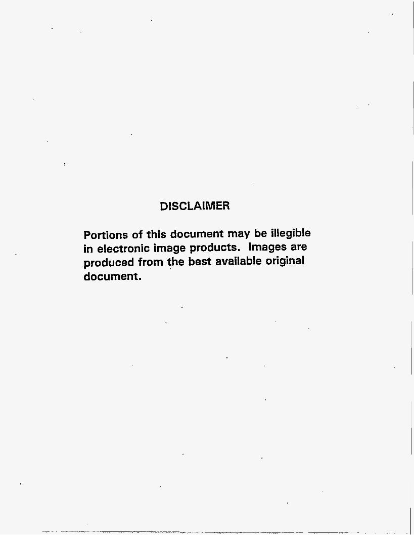
Figures 3 and 4 show I-V characteristics of both unstressed and stressed devices. The forward characteristics shown in figure 3 show both the I-V data for forward bias as well as the resistance (forward voltage divided by forward current). The I-V curves show a small difference, mostly a stress induced increase in conductivity at voltages below the
. . . 1.. ...... . . ~ ...... ..
I
threshold voltage (-2.8 V). The resistance curves support this observation by showing a fairly constant resistance of about 10 kQ for the degraded device versus several orders of magnitude greater resistance for the unstressed device. As expected, the difference between the two resistance curves is reduced after turn-on as the resistance across the junction will be very small compared to any other parallel resistance path. The reverse bias curves in figure 4 show a more dramatic difference. In this case, the normally small leakages found across reverse biased junctions are easily distinguishable from the ohmic path found across the stressed LED.
20
16
n Q E
E
0 101 0 0.7 1.4 2.1 2.8 3.5
Forward Voltage, VF (V)
Figure 3 - Forward I-V characteristics and resistances of a stressed and an unstressed LED.
-100
2 -80
-60 +
u -40
% p! -20 0
0 -1 -2 -3 -4 -5 Reverse Voltage (V)
Figure 4 - Reverse I-V characteristics of one stressed and three unstressed LEDs.
In order to understand the physical phenomenon responsible for the changes in the characteristics of LEDs that have been subjected to high current stresses, several different tests were done.
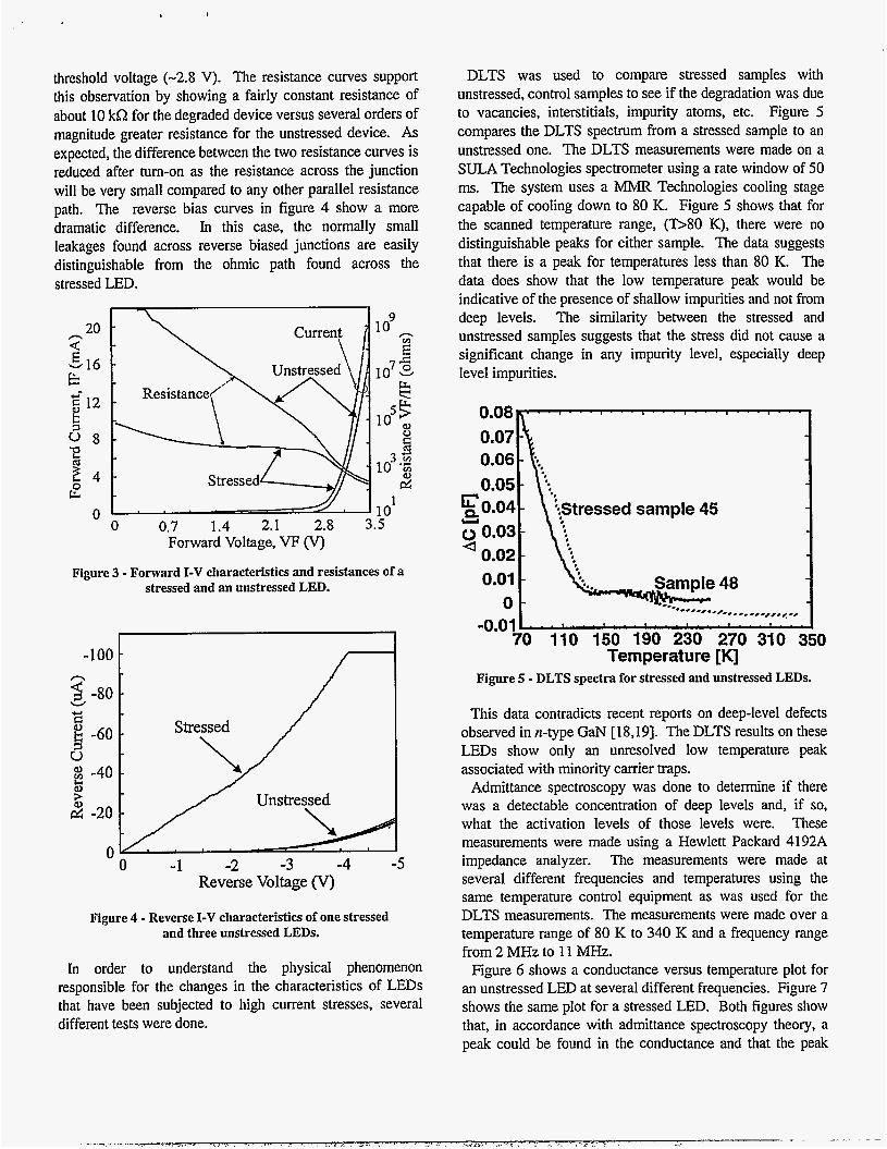
DLTS was used to compare stressed samples with unstressed, control samples to see if the degradation was due to vacancies, interstitials, impurity atoms, etc. Figure 5 compares the DLTS spectrum from a stressed sample to an unstressed one. The DLTS measurements were made on a SULA Technologies spectrometer using a rate window of 50 ms. The system uses a MMR Technologies cooling stage capable of cooling down to 80 K. Figure 5 shows that for the scanned temperature range, (E40 K), there were no distinguishable peaks for either sample. The data suggests that there is a peak for temperatures less than 80 K. The data does show that the low temperature peak would be indicative of the presence of shallow impurities and not from deep levels. The similarity between the stressed and unstressed samples suggests that the stress did not cause a significant change in any impurity level, especially deep level impurities.
0.06
Y \ressed sample 45 0 0.03
0.02
Sample 48
, . . . , , , . , . , , -0.01 70 110 150 190 230 270 310 350
Temperature [Kl
. . . , , ***--.*--R- ....e*-,,. e.*
Figure 5 - DLTS spectra for stressed and unstressed LEDs.
This data contradicts recent reports on deep-level defects observed in n-type GaN [18,19]. The DLTS results on these LEDs show only an unresolved low temperature peak associated with minority carrier traps.
Admittance spectroscopy was done to determine if there was a detectable concentration of deep levels and, if so, what the activation levels of those levels were. These measurements were made using a Hewlett Packard 4192A impedance analyzer. The measurements were made at several different frequencies and temperatures using the same temperature control equipment as was used for the DLTS measurements. The measurements were made over a temperature range of 80 K to 340 K and a frequency range from 2 MHZ to 11 MHz.
Figure 6 shows a conductance versus temperature plot for an unstressed LED at several different frequencies. Figure 7 shows the same plot for a stressed LED. Both figures show that, in accordance with admittance spectroscopy theory, a peak could be found in the conductance and that the peak
shifted to higher temperatures with higher frequencies to higher temperatures. From these data, an Arrhenious plot can be made whose slope gives the activation energy AE=J+Ev, where ET is the energy level of the trap and Ev is the valence band energy. Figure 8 shows the Arrhenious plots for both the stressed and unstressed LEDs. From this figure, activation energies of 91 meV for the stressed LED and 77 meV for the unstressed LED are obtained. These results also indicate that no deep levels were detected, only shallow ones. The difference in activation energies is insignificant as the difference is within the standard deviation of the measurement on this system. These activation energies most likely correspond to the low temperature DLTS peak from figure 5 and are virtually unaffected by electrical stress.
2510'
50 100 150 200 250 300 350 Temperature IKl
kll.1 M H z
- rl f j 0 .1 MM
c - 2 0
h 0 Id
m a E: 1.0
L
7 3
0" 51)
0.m
-..- /; ._...-....._._ ..._.. .... .....e.-
t , I"
100 150 200 250 300 Temperature T [Kl
1 '= r t 8.1
1- 7.1
1;: 6.1
h 5.1
I= 4.1
fs 3.1
4 I
J 1 I
I= L - 1.11.1
350
lam
MHr
MHr
M M
MHr
HHr
MHr
MHZ
YHz
5-01 -\. - 4.8: tu X AE = 77 meV 2 4.6: - 4 . 4 -
4 .2 1
4.0 1
's I= -
AE = 91 meV
1/T max [ lo4 K"] Figure 8 - Arrhenious plots from admittance spectroscopy data
for both stressed and unstressed LEDs.
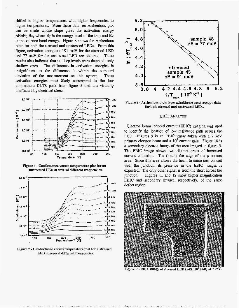
EBIC ANALYSIS
Electron beam induced current (EBIC) imaging was used to identify the location of low resistance path across the LED. Figures 9 is an EBIC image taken with a 7 keV primary electron beam and a lo9 current gain. Figure 10 is a secondary electron image of the area imaged in figure 9. The EBIC image shows two distinct areas of increased current collection. The first is the edge of the p-contact area. Since this area allows the beam to come into contact with the junction, its presence in the EBIC images is expected. The only other signal is from the short across the junction. Figures 11 and 12 show higher magnification EBIC and secondary images, respectively, of the same defect region.
Figure 7 - Conductance versus temperature plot for a stressed LED at several different frequencies.
Figure 9 - EBIC image of stressed LED (54X, 10'gain) at 7 keV.
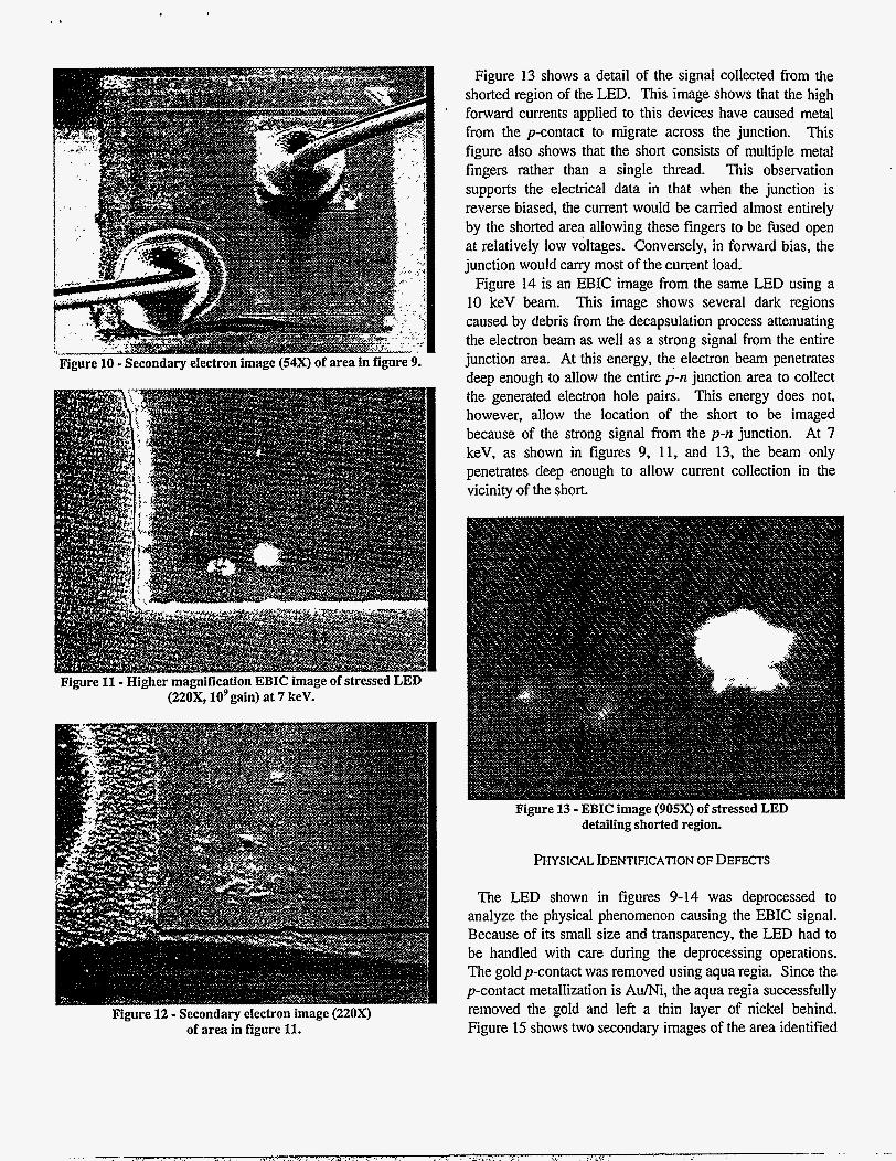
Figure 10 - Secondary ' electron image (34A) 01 area in figure 9.
Figure 11 - Higher magnification EBIC image of stressed LED (220X, lo9 gain) at 7 keV.
Figure 13 shows a detail of the signal collected from the shorted region of the LED. This image shows that the high forward currents applied to this devices have caused metal from the p-contact to migrate across the junction. This figure also shows that the short consists of multiple metal fingers rather than a single thread. This observation supports the electrical data in that when the junction is reverse biased, the current would be carried almost entirely by the shorted area allowing these fingers to be fused open at relatively low voltages. Conversely, in forward bias, the junction would carry most of the current load.
Figure 14 is an EBIC image from the same LED using a 10 keV beam. This image shows several dark regions caused by debris from the decapsulation process attenuating the electron beam as well as a strong signal from the entire junction area. At this energy, the electron beam penetrates deep enough to allow the entire F n junction area to collect the generated electron hole pairs. This energy does not, however, allow the location of the short to be imaged because of the strong signal from the p-n junction. At 7 keV, as shown in figures 9, 11, and 13, the beam only penetrates deep enough to allow current collection in the vicinity of the short.
PHYSICAL IDENTIFICATION OF DEFECTS
The LED shown in figures 9-14 was deprocessed to analyze the physical phenomenon causing the EBIC signal. Because of its small size and transparency, the LED had to be handled with care during the deprocessing operations. The gold p-contact was removed using aqua regia. Since the p-contact metallization is A m i , the aqua regia successfully removed the gold and left a thin layer of nickel behind. Figure 15 shows two secondary images of the area identified

using EBIC. The images clearly show that metal has
:d LED (430X, lo9 gainj at 10 keV.
U1l;UlG Ad- "Gb"..uulJ ... L U 6 W v. Y..V.CI.. -1- u.. Il -"...Act removal. Top image is 2500X, bottom image is 7500X.
TEM ANALYSIS
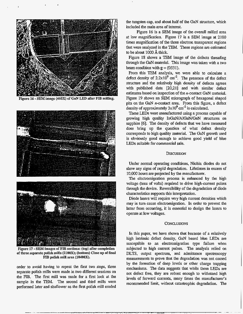
As the main premise of this study was that the electromigration of contact metals was along crystalline defects or defect tubes, we needed to understand and quantify the defect density present in these devices. The best method to accomplish this was through the use of the transmission electron microscope ( E M ) . Since we only had single, packaged LEDs, we had to prepare tiny samples for cross section TEM analysis. The only way to accomplish this was with a focused ion beam system (FIB).
The main concerns with using a FIB for TEM sample preparation are the implantation of Ga into the sample and the creation of defects during the milling process. Even though the Ga beam is not scanned directly on the surface that will be studied in the TEM, enough Ga is implanted because of backscattered primary ions that its presence is observed. Several failure analysis facilities only use a FIB for TEM sample preparation when other, conventional methods are not feasible, which was the case for this work.
The first step in the sample preparation process was to mechanically thin the sample as much as possible to reduce the FIB milling time. After the LED was removed from its package, it was mounted on a polishing stub with wax. The sample was thinned on both sides (to allow examination of a specific region on the LED) using 600 grit sandpaper to a width of about 160 pm. The sliver was then transferred to a piece of scrap silicon that had been cut to a half-circle 3 mm in diameter and again held in place with wax. The silicon was to be the holder for the LED for both the FIB work and for analysis in the TEM.
The FIB work consisted of the deposition of a protective tungsten cap layer followed by three separate types of mills, all using a 30 keV primary ion beam. The tungsten layer was approximately 5 pm wide by 1 pm thick and was deposited to protect the top surface of the TEM section.
The first, or rough mill was designed to remove as much of the GaN material in as short a time as possible. For this process, a large, 750 pm, aperture was used and a mill dose selected to cut to a depth of about 15 pm. Since we wanted to analyze a specific part of the LED, all three mills had to be done twice, once from each side. In all, an area of about 50 pm by 160 pm was milled to 15 pm depth.
The second series of mills were performed with a 400 pm aperture. This aperture allows more precise control of the mill process but slows the rate at which material is removed. The mills done in this phase were the full 50 pm wide and 15 pm deep, but only about 5 pm long (with long refemng to the dimension normal to the TEM sample area).
Finally, several regions were milled using a polish mill. For this, a 100 pm aperture was selected to allow precise control of the beam as well as a finely polished surface. In
c of three separate polish mills (2100X); (bottom) Close up of final
FIB polish mill area (10400X).
order to avoid having to repeat the first two steps, three separate polish mills were made in two different sessions on the FIB. The first mill was made for a first look at the sample in the "EM. The second and third mills were performed later and shallower as the first polish mill eroded
the tungsten cap, and about half of the GaN structure, which included the main area of interest.
Figure 16 is a SEM image of the overall milled area at low magnification. Figure 17 is a SEM image at 2100 times magnification of the three electron transparent regions that were analyzed in the TEM. These regions are estimated to be about 1000 Athick.
Figure 18 shows a TEM image of the defects threading through the GaN material. This image was taken with a two beam condition with g = (033 1).
From this TEM analysis, we were able to calculate a defect density of 2 .2~10~ The presence of the defect structure and the relatively high density of defects agrees with published data [20,21] and with similar defect estimates based on inspection of the n-contact GaN material. Figure 19 shows an SEM micrograph of hexagonal shaped pits on the GaN n-contact area. From this figure, a defect density of approximately 3x109 cm-2 is calculated.
These LEDs were manufactured using a process capable of growing high quality InGaN/AlGaN/GaN structures on sapphire [6]. The density of defects that we have measured does bring up the question of what defect density corresponds to high quality material. The GaN growth used is obviously good enough to achieve good yield of blue LEDs suitable for commercial sale.
DISCUSSION
Under normal operating conditions, Nichia diodes do not show any signs of rapid degradation. Lifetimes in excess of 10,OOO hours are projected by the manufacturer. The electromigration process is enhanced by the high
voltage (tens of volts) required to drive high-current pulses through the device. Reversibility of the degradation of diode characteristics supports this interpretation.
Diode lasers will require very high current densities which may in turn cause electromigration. In order to prevent the latter from occurring, it is essential to design the lasers to operate at low voltages.
CONCLUSIONS
In this paper, we have shown that because of a relatively high intrinsic defect density, GaN based blue LEDs are susceptible to an electromigration type failure when subjected to high current pulses. The analysis relied on DLTS, output spectrum, and admittance spectroscopy measurements to prove that the degradation was not caused by the formation of deep levels or other charge trapping mechanisms. The data suggests that while these LEDs are not defect free, they are robust enough to withstand high levels of forward currents, many times the manufacturer's recommended limit, without catastrophic degradation. The

presence of a large, 2 . 2 ~ 1 0 ~ cme2, density of defects decreases the resistance of the LED to electromigration type failure modes. Progress toward defect free GaN layer growth is necessary for the use of group-I11 nitrides in the manufacture of blue semiconductor lasers. Since these devices are normally operated at much higher current and photon densities, they will be more sensitive to the presence of crystalline defects.
kX at 200 keV).
ACKNOWLEDGMENTS
The authors would like to thank Ann Campbell and Jim Rife at Sandia National Laboratories for the preparation of the TEM sample using the focused ion beam system, Lumin Wang at the University of New Mexico for assistance with the TEM analysis, and Ann N. Campbell, Edward I. Cole, Jr., William M. Miller, Kenneth A. Peterson, and Paiboon Tangyungyong for reviewing this manuscript. This work was supported by ARPA, by the New Energy and Industrial Technology Development Organization (NEDO) of Japan and, at Sandia National Laboratories, by the U.S. Department of Energy under contract DE-AC04-94AL8500.
n-contact layer.
REFERENCES
S . Nakamura, T. Mukai, M. Senoh, “Candela-Class High-Brightness InGaN/AlGaN Double-Heterostruct- ure Blue-Light-Emitting Diodes,” Appl. Phys. Leu.. Vol. 64, No. 13,28 March 1994, p. 1687. S. Strite, and H. MorkoG, “GaN, AIN. and InN: A Review, J . Vuc. Sci. Technol. B 10(4), JuVAug 1992, p. 1237.
[3] S . Strite, “GaN Core Relaxation Effects and Their Ramifications for P-Type Doping,” Jup. J. Appl. Phys.. Vol. 33, No. SB, 15 May 1994, p. L699.
[4] S. Nakamura, N. Iwasa, and S. Nagahama, “Cd-Doped InGaN Films Grown on GaN Films,’’ Jap. J. Appl. Phys., Vol. 32, No. 3A, 1 March 1993, p. L338.
[SI S. Nakamura, and T. Mukai, and M. Senoh, “Si-Doped InGaN Films Grown on GaN Films,” Jap. J. Appl. Phys., Vol. 32, No. lA/B, 15 January 1993, p. L16.
[6] S. Nakamura, and T. Mukai, “High-Quality InGaN Films Grown on GaN Films,” Jap. J. Appl. Phys., Vol. 3 1, No. 1 OB. 15 October 1992. p. L 1457.
[7] S . Nakamura, T. Mukai. M. Senoh, and N. Iwasa, “Thermal Annealing Effects on P-Type Mg-Doped GaN Films,’‘ Jup. J . Appl. Phys., Vol. 31. No. 2B, 15 February 1992, p. L139.
[8] S. Nakamura, M. Senoh, and T. Mukai, “Highly P- Typed Mg-Doped GaN Films Grown with GaN Buffer Layers,” Jup. J . Appl. Phys., Vol. 30, No. IOA, October 199 1, p. L 1708.
[9] S. Nakamura. “GaN Growth Using GaN Buffer Layer,” Jap. J. Appl. Phys., Vol. 30, No. IOA, October 1991, p. L1705.

[lo] S. Nakamura, , N. Iwasa, M. Senoh, and, T. Mukai, “Hole Compensation of P-Type GaN Films,” Jup. J. Appl. Phys., Vol. 31, No. 5A, May 1992, p. 1258.
[ l l ] S. Nakamura, Y. Harada, and M. Seno, “Novel Metalorganic Chemical Vapor Deposition System for GaN Growth,” Appl. Phys. Lett., Vol. 58, No. 18, 6 May 1991, p. 2021.
[12] N. Yashimoto, T. Matsuoka, and A. Katsui, “Photoluminescence of InGaN Films Grown at High Temperature by Metalorganic Vapor Phase Epitaxy,” Appl. Phys. Lett., Vol. 59, No. 18,28 October 1991, p. 225 1.
[13] S. Strite, J. Ruan, 2. Li, A. Salvador, H. Chen, D. Smith, W. Choyke, and H. MorkoF, “An Investigation of the Properties of Cubic GaN Grown on GaAs by Plasma-Assisted Molecular-Beam Epitaxy,” J. Vac. Sci. Technol., Vol. 9, No. 4, July/August 1991, p. 1924.
[14] S. Nakamura, T. Mukai, and M. Senoh, “High-Power GaN P-N Junction Blue-Light-Emitting Diodes,” Jap. J. Appl. Phys., Vol. 30, No. 12A, December 1991, p. L1998.
[15] S. Nakamura, M. Senoh, and T. Mukai, “P-GaN/N- InGaN/N-GaN Double-Heterostructure Blue-Light- Emitting Diodes,” Jap. J. Appl. Phys., Vol. 32, No. lAh3, January 1993, p. L8.
[16] S. Nakamura, M. Senoh, and T. Mukai, “High-Power InGaN/GaN Double-Heterostructure Violet Light Emitting Diodes,” Appl. Phys. Lett., Vol. 62, No. 19, 10 May 1993, p. 2390.
[17] S. Nakamura, 2nd Workshop on Wide Bandgap Nitrides, St. Louis, MO., October 17-18, 1994.
[18] P. Hacke, T. Detchprohm, K. Hiramatsu, N. Sawaki, K. Tadatomo, and K. Miyake, “Analysis of Deep Devels in n-type GaN by Transient Capacitance Methods,” J. Appl. Phys., Vol. 76, No. 1, 1 July 1994, p. 304.
[19] W. Gotz, N. Johnson, H. Amano, and I. Akasaki, “Deep Level Defects in n-type GaN,” Appl. Phys. Lett., Vol. 65, No. 4,25 July 1994, p. 463.
[20]T. Humphries, C. Sukow, R. Nemanich, J. Posthill, R. Rudder, S. Hattangady, and R. Markunas, “Micorstructural and Optical Characterization of GaN Films Grown by PECVD on (0001) Sapphire Substrates,” Mat. Res. SOC. Symp. Proc.. Vol. 162, 1990, p. 531.
[21] 2. Sitar, M. Paisley, and R. Davis, “Structural Defects in GaN Epilayers Grown by Gas Source Molecular Beam Epitaxy,” Mat. Res. SOC. Symp. Proc. Vol. 162, 1990, p. 537.
Related Documents