DC Optimizer for PV Module by Daniel Luster A Thesis Presented in Partial Fulfillment of the Requirements for the Degree Master of Science Approved November 2014 by the Graduate Supervisory Committee: Raja Ayyanar, Chair Bertan Bakkaloglu Sayfe Kiaei ARIZONA STATE UNIVERSITY December 2014

Welcome message from author
This document is posted to help you gain knowledge. Please leave a comment to let me know what you think about it! Share it to your friends and learn new things together.
Transcript
DC Optimizer for PV Module
by
Daniel Luster
A Thesis Presented in Partial Fulfillment of the Requirements for the Degree
Master of Science
Approved November 2014 by the Graduate Supervisory Committee:
Raja Ayyanar, Chair Bertan Bakkaloglu
Sayfe Kiaei
ARIZONA STATE UNIVERSITY
December 2014
i
ABSTRACT
As residential photovoltaic (PV) systems become more and more common and
widespread, their system architectures are being developed to maximize power extraction
while keeping the cost of associated electronics to a minimum. An architecture that has
become popular in recent years is the “DC optimizer” architecture, wherein one DC-DC
converter is connected to the output of each PV module. The DC optimizer architecture
has the advantage of performing maximum power-point tracking (MPPT) at the module
level, without the high cost of using an inverter on each module (the "microinverter"
architecture). This work details the design of a proposed DC optimizer. The design
incorporates a series-input parallel-output topology to implement MPPT at the sub-
module level. This topology has some advantages over the more common series-output
DC optimizer, including relaxed requirements for the system’s inverter. An autonomous
control scheme is proposed for the series-connected converters, so that no external
control signals are needed for the system to operate, other than sunlight. The DC
optimizer in this work is designed with an emphasis on efficiency, and to that end it uses
GaN FETs and an active clamp technique to reduce switching and conduction losses. As
with any parallel-output converter, phase interleaving is essential to minimize output
RMS current losses. This work proposes a novel phase-locked loop (PLL) technique to
achieve interleaving among the series-input converters.
ii
TABLE OF CONTENTS
Page
LIST OF TABLES ……………………………………………………………………… v
LIST OF FIGURES …………………………………………………...………...……… vi
CHAPTER
1 INTRODUCTION AND THESIS OUTLINE …………………………………….….. 1
1.1 Introduction to Photovoltaic Energy Conversion …………………………. 1
1.2 Thesis Objective and Outline ………………………………………..……. 7
2 PV CELL MODELING ………………………………………………………...…….. 9
2.1 Brief Description of PV Cell Operation …………………………………… 9
2.2 Modeling PV Cell ………………………..……………………………….. 11
2.3 Bypass Diodes and 72-Cell PV Module ........………………………………17
3 ARCHITECTURES FOR RESIDENTIAL PV SYSTEMS ……………………….... 20
3.1 Introduction ……………………………………………………………….. 20
3.2 Common Architectures for Residential PV Systems …………………….... 20
3.3 Recent Developments in DC Optimizers ………………………………..… 24
4 SUB-MODULE MPPT …………………………………………………………….... 26
4.1 Introduction to Sub-Podule MPPT …………......…………………………. 26
4.2 Calculation of Power Gain for Real Module …………...……………….… 28
5 PROPOSED DC OPTIMIZER AND CONTROL ARCHITECTURE …………..…. 32
5.1 Proposed DC Optimizer …………………………………………………… 32
5.2 Derivation of Proposed Converter …………………………….…………... 33
5.3 Effect on System ……………………………………………………..…… 39
iii
CHAPTER Page
5.4 Proposed Control Circuit Architecture ……...…………………………….. 41
6 EFFICIENCY IMPROVEMENT WITH ACTIVE CLAMP …………………..…… 45
6.1 Energy Loss in Flyback Converter ……………………………………..….. 45
6.2 Steady-state Operation of Active Clamp Flyback Converter …………….… 47
6.3 Derivation of Design Constraints ………………………………………..… 54
6.4 Stability of Clamp Voltage ………………………………………………... 60
7 EFFICIENCY IMPROVEMENT WITH GAN FETS ………………………………..65
7.1 Introduction ……………………………………………………………….. 65
7.2 eGaN FET Properties ……………………………………………………… 67
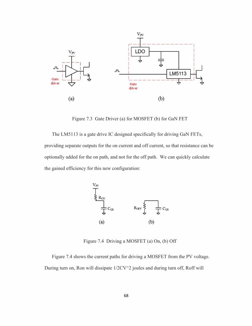
7.3 Design of Gate Driver for Q1 ………………………………………………. 67
7.4 Design of Gate Driver for Q2 ………………………………………………. 70
8 POWER STAGE CALCULATIONS …………………………………………….…. 71
8.1 Outline of Calculations ………………………………………….………... 71
8.2 Input Voltage and Current Cange …………………………………..…….. 71
8.3 Choice of Switching Frequency, Duty and Turns Ratio ………………….. 70
8.4 Selection of Leakage Inductance Llk and Magnetizing Inductance Lm ….. 73
8.5 Selection of Ccl ………………………………………………………….… 77
9 MODELING AND SIMULATION OF ACTIVE CLAMP FLYBACK ………...… 79
9.1 Discussion on Modeling and Simulation………………………………...… 79
9.2 PWL Model of PV Sub-Module………………………………...…............ .79
9.3 Model of GaN FET………………………………...…............................... ..83
9.4 Model of Flyback Transformer………………………………...…............ ...86

iv
CHAPTER Page
9.5 Model of PWM Block and Gate Driver………………………………..........87
9.6 Complete Circuit….................................……………………………...........88
9.7 Simulation Waveforms………………………………..................................89
10 PHASE-LOCKED LOOP FOR CONVERTER INTERLEAVING..........................95
10.1 Desire for Phase Interleaving......................................................................95
10.2 Typical Interleaving Technique with PWM Synchronization....................98
10.3 Timing Pin on ISL8130..............................................................................98
10.4 Proposed Phase-Locked Loop....................................................................99
10.5 Simulation of PLL.....................................................................................101
11 DISCUSSION AND CONCLUSIONS...................................................................106
REFERENCES …………………...........………………………………………………108

v
LIST OF TABLES
TABLE Page
2.1 Solar Module Specifications ……………………………………………………..... 12
2.2 Comparison of Actual and Modeled PV Values …..………………………………. 17
6.1 Summary of Design Constraints ………………………………………………….... 64
vi
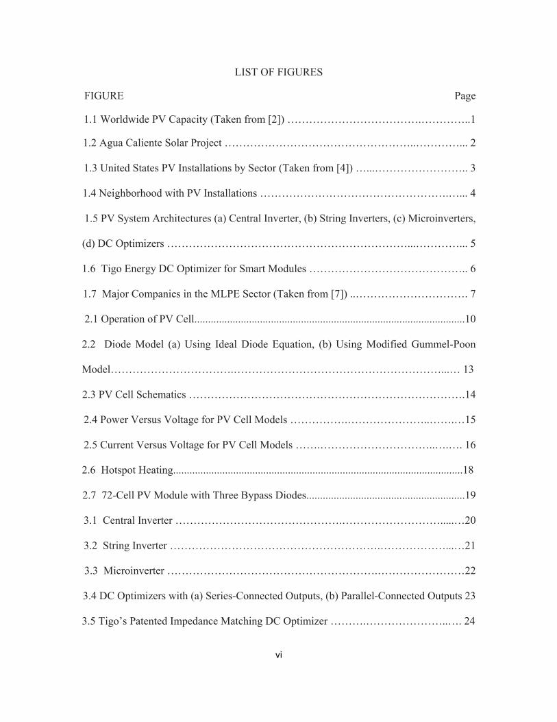
LIST OF FIGURES
FIGURE Page
1.1 Worldwide PV Capacity (Taken from [2]) ……………………………….…………..1
1.2 Agua Caliente Solar Project ……………………………………………..…………... 2
1.3 United States PV Installations by Sector (Taken from [4]) …...…………………….. 3
1.4 Neighborhood with PV Installations …………………………………………….…... 4
1.5 PV System Architectures (a) Central Inverter, (b) String Inverters, (c) Microinverters,
(d) DC Optimizers …………………………………………………………...…………... 5
1.6 Tigo Energy DC Optimizer for Smart Modules …………………………………….. 6
1.7 Major Companies in the MLPE Sector (Taken from [7]) ..…………………………. 7
2.1 Operation of PV Cell...................................................................................................10
2.2 Diode Model (a) Using Ideal Diode Equation, (b) Using Modified Gummel-Poon
Model…………………………….…………………………………………………...… 13
2.3 PV Cell Schematics ………………………………………………………………….14
2.4 Power Versus Voltage for PV Cell Models …………….…………………..…….…15
2.5 Current Versus Voltage for PV Cell Models …….…………………………..….…. 16
2.6 Hotspot Heating..........................................................................................................18
2.7 72-Cell PV Module with Three Bypass Diodes..........................................................19
3.1 Central Inverter ……………………………………….……………………….....…20
3.2 String Inverter ………………………………………………….………………...…21
3.3 Microinverter ………………………………………………….……………………22
3.4 DC Optimizers with (a) Series-Connected Outputs, (b) Parallel-Connected Outputs 23
3.5 Tigo’s Patented Impedance Matching DC Optimizer ……….…………………..…. 24

vii
FIGURE Page
3.6 Parallel-Ladder Current-Shuffling DC Optimizer ………...……………………..… 25
3.7 Synchronous Buck Converters at Sub-Module Level ……………………………... 25
4.1 Using Simplified Diode Model to Visualize Mismatch of Series Cells ………….. 26
4.2 Power extraction from Two Series Strings of PV Cells with (a) Minimum Current,
(b) Use of Bypass Diode, (c) Sub-Module MPPT …………………………………….. 27
4.3 Power Extraction from Three Series Strings of PV Cells (a) at Minimum Current, (b)
One Bypass Diode Conducting, (c) Two Bypass Diodes Conducting, (d) Using Sub-
Module MPPT ……………………………………………………………..…………... 28
4.4 Power Extraction During Mismatch Scenario 1 …………………………………... 29
4.5 Power Extraction During Mismatch Scenario 2 ……………...…………………… 30
5.1 Series-Input Parallel-Output Flyback Converter …….……………………………. 32
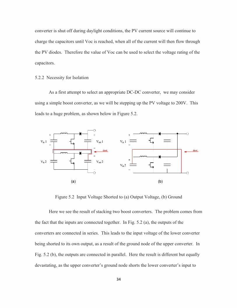
5.2 Input Voltage Shorted to (a) Output Voltage, (b) Ground ……..…………………. 34
5.3 Series-Input Isolated Converters with (a) Series-Connected Outputs, (b) Parallel-
Connected Outputs …………….…………………………………………………….… 35
5.4 Stages of Converter Turn-Off. (a) Normal Conditions, (b) Capacitor Forced to Zero,
(c) Capacitor Forced Negative, (d) Output Diode Forward Biased ……….…………… 38
5.5 DC Optimizers connected in parallel …………………………………………….... 40
5.6 Control Architecture ……………...……………………………………………….. 41
5.7 Using UVLO to Turn On/Off Converter with Sunlight ………..………………….. 43
6.1 Flyback Converter …..…………………………………………………………….. 45
6.2 Flyback Converter with RCD Clamp ……………………………………..………. 46
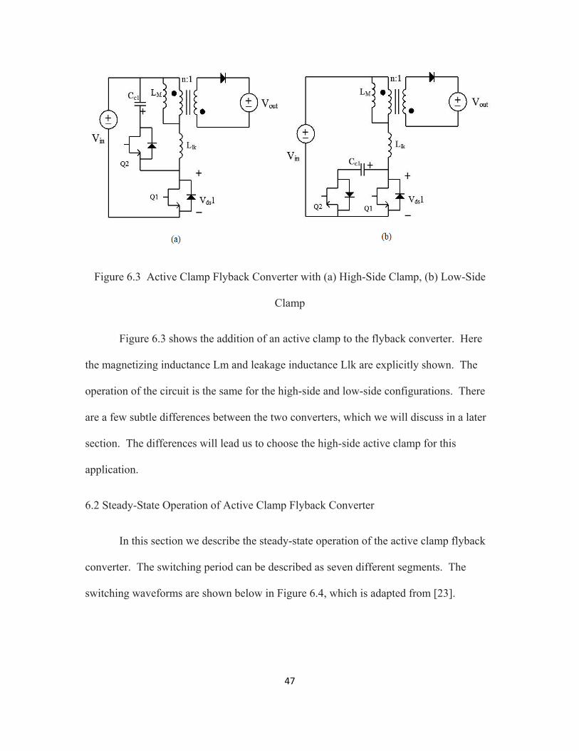
6.3 Active Clamp Flyback Converter with (a) High-Side Clamp, (b) Low-Side Clamp.47
viii
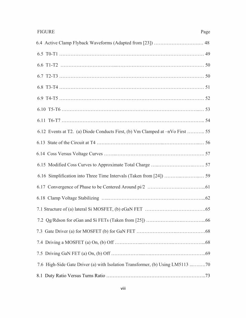
FIGURE Page
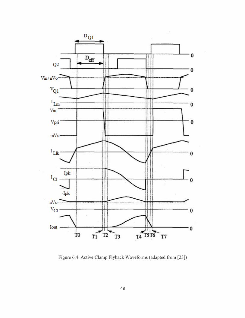
6.4 Active Clamp Flyback Waveforms (Adapted from [23]) ……………………….… 48
6.5 T0-T1 ……………………………………………………………………………… 49
6.6 T1-T2 ……………………………...……………………………………………… 50
6.7 T2-T3 ……………………………………………………………………………… 50
6.8 T3-T4 ……………………………………………………………………………… 51
6.9 T4-T5 ……………………………………………………………………………… 52
6.10 T5-T6 …………………………………………………………………………..… 53
6.11 T6-T7 …………………………………………………………………………….. 54
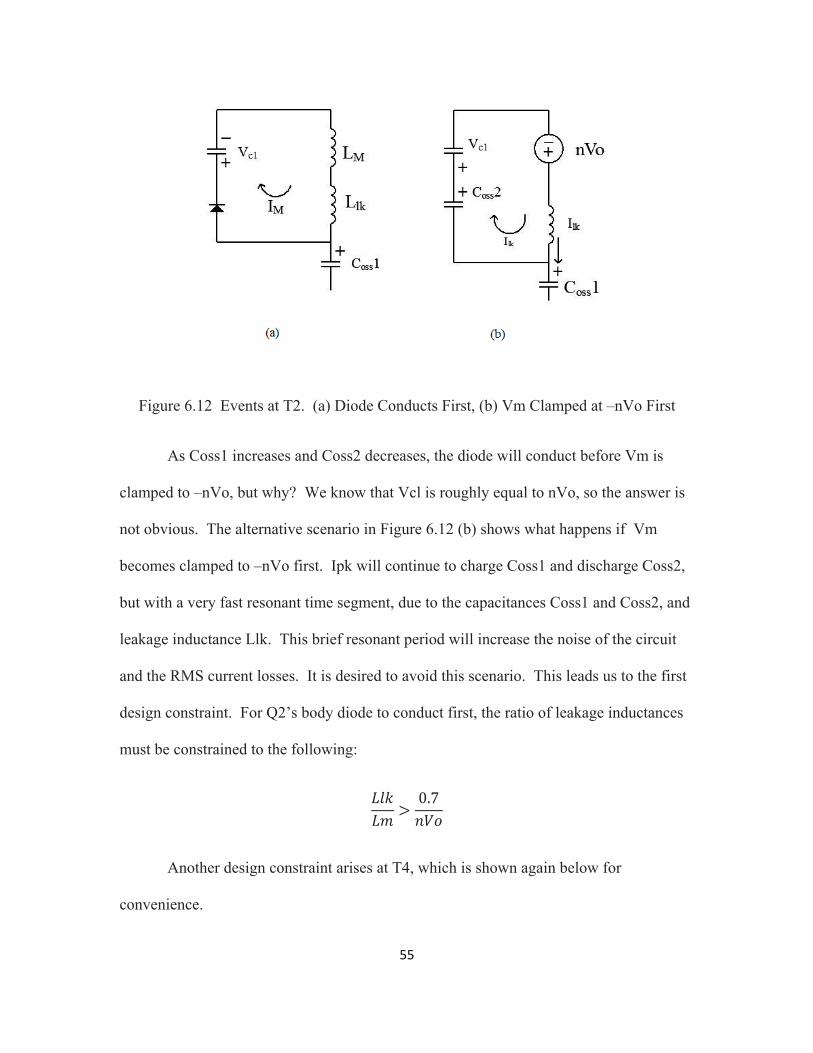
6.12 Events at T2. (a) Diode Conducts First, (b) Vm Clamped at –nVo First ……….. 55
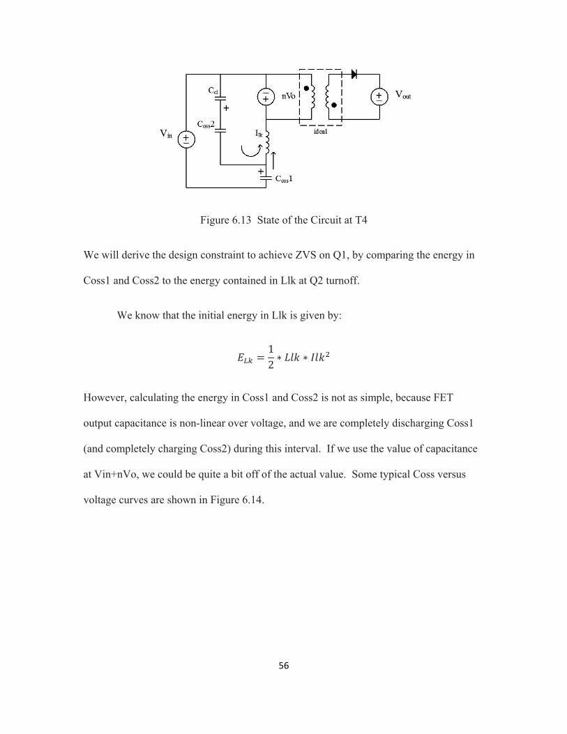
6.13 State of the Circuit at T4 …….……………………………..…………………..… 56
6.14 Coss Versus Voltage Curves ……..………………………………………………. 57
6.15 Modified Coss Curves to Approximate Total Charge …..………………….……. 57
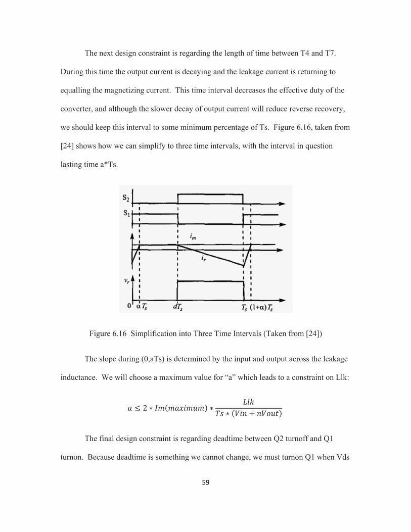
6.16 Simplification into Three Time Intervals (Taken from [24]) ………..….……..… 59
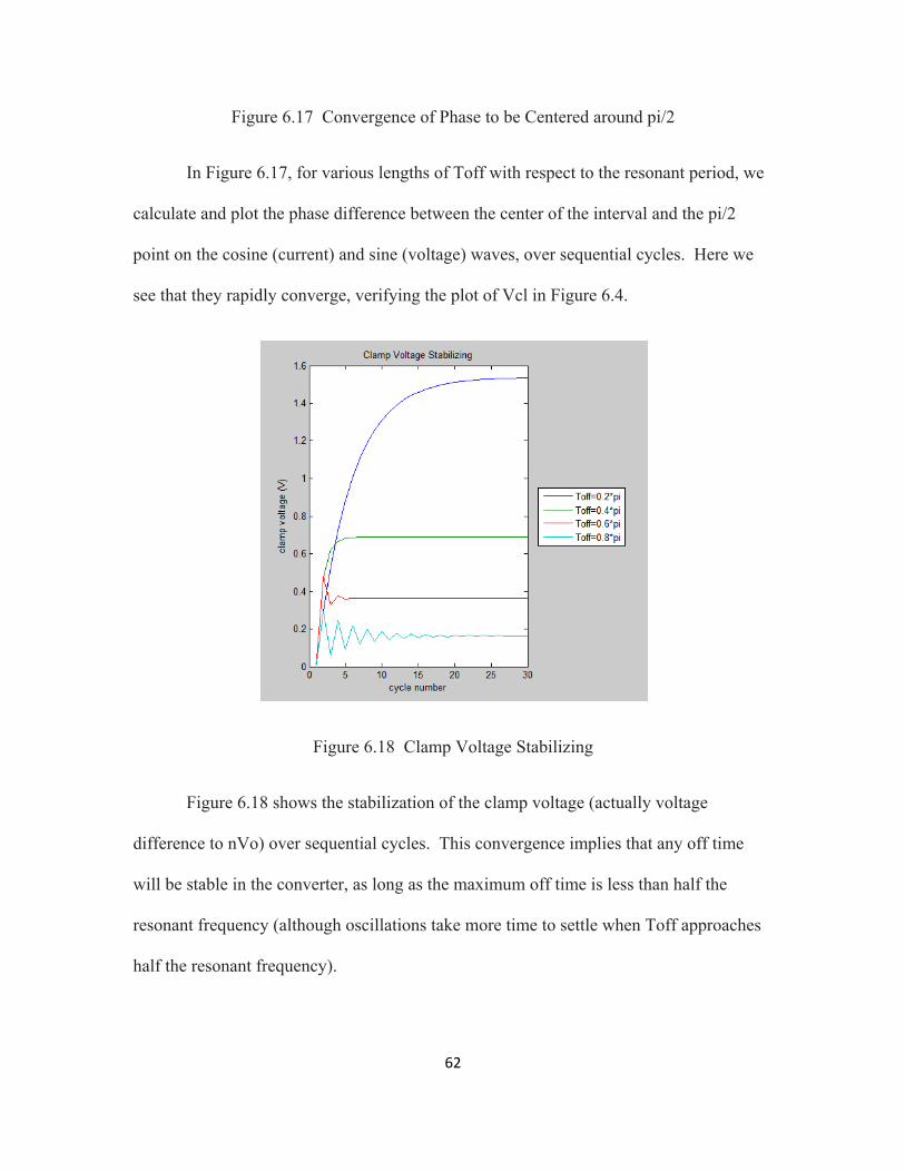
6.17 Convergence of Phase to be Centered Around pi/2 ……………….……………...61
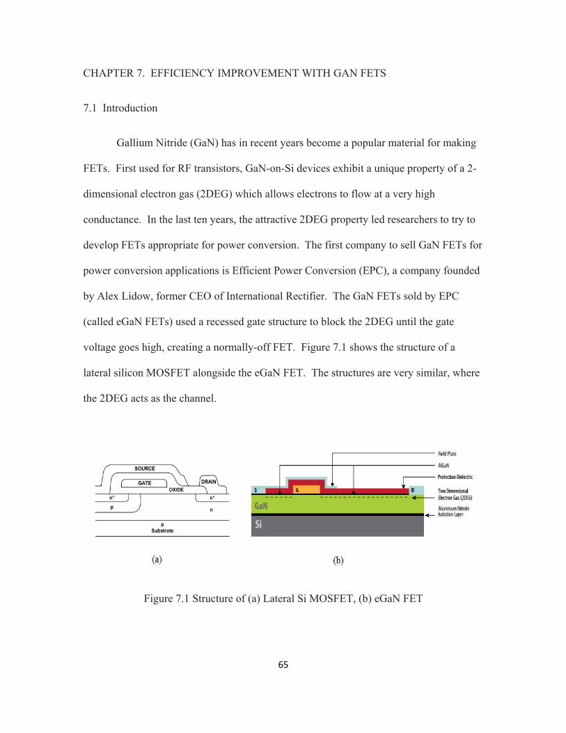
6.18 Clamp Voltage Stabilizing …..………………………………….………………...62
7.1 Structure of (a) lateral Si MOSFET, (b) eGaN FET ……………….……………….65
7.2 Qg/Rdson for eGan and Si FETs (Taken from [25]) …………….…….…………...66
7.3 Gate Driver (a) for MOSFET (b) for GaN FET …………………….………………68
7.4 Driving a MOSFET (a) On, (b) Off ……………...……………….………………...68
7.5 Driving GaN FET (a) On, (b) Off ………………...….……………………………..69
7.6 High-Side Gate Driver (a) with Isolation Transformer, (b) Using LM5113 ...….….70
8.1 Duty Ratio Versus Turns Ratio ……………………………………………………..73
ix
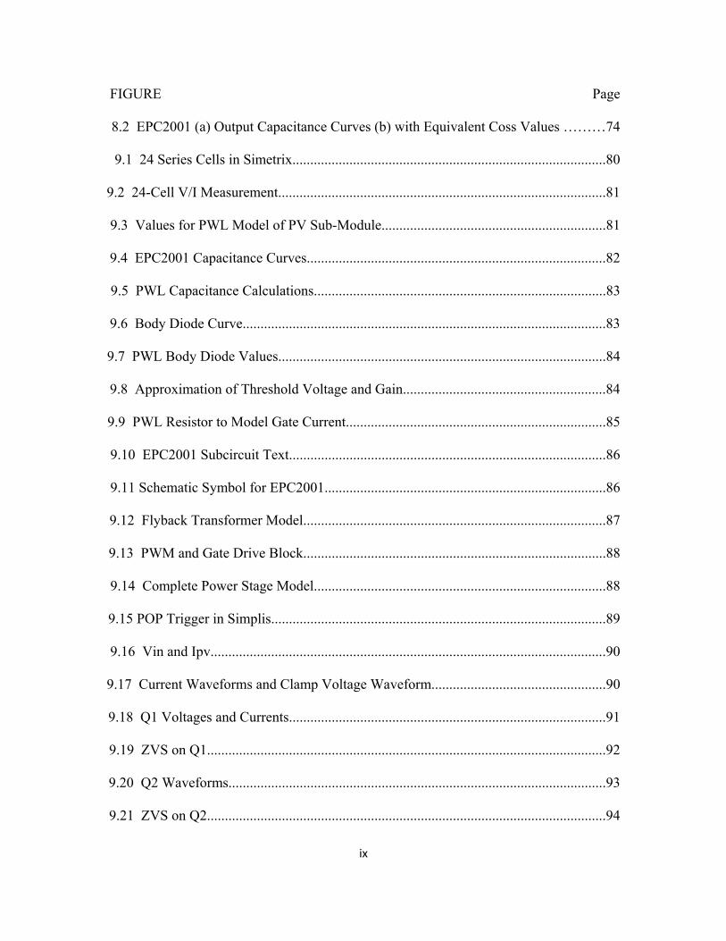
FIGURE Page
8.2 EPC2001 (a) Output Capacitance Curves (b) with Equivalent Coss Values ………74
9.1 24 Series Cells in Simetrix........................................................................................80
9.2 24-Cell V/I Measurement............................................................................................81
9.3 Values for PWL Model of PV Sub-Module...............................................................81
9.4 EPC2001 Capacitance Curves....................................................................................82
9.5 PWL Capacitance Calculations..................................................................................83
9.6 Body Diode Curve......................................................................................................83
9.7 PWL Body Diode Values............................................................................................84
9.8 Approximation of Threshold Voltage and Gain.........................................................84
9.9 PWL Resistor to Model Gate Current.........................................................................85
9.10 EPC2001 Subcircuit Text.........................................................................................86
9.11 Schematic Symbol for EPC2001...............................................................................86
9.12 Flyback Transformer Model.....................................................................................87
9.13 PWM and Gate Drive Block.....................................................................................88
9.14 Complete Power Stage Model..................................................................................88
9.15 POP Trigger in Simplis..............................................................................................89
9.16 Vin and Ipv...............................................................................................................90
9.17 Current Waveforms and Clamp Voltage Waveform.................................................90
9.18 Q1 Voltages and Currents.........................................................................................91
9.19 ZVS on Q1................................................................................................................92
9.20 Q2 Waveforms..........................................................................................................93
9.21 ZVS on Q2................................................................................................................94
x
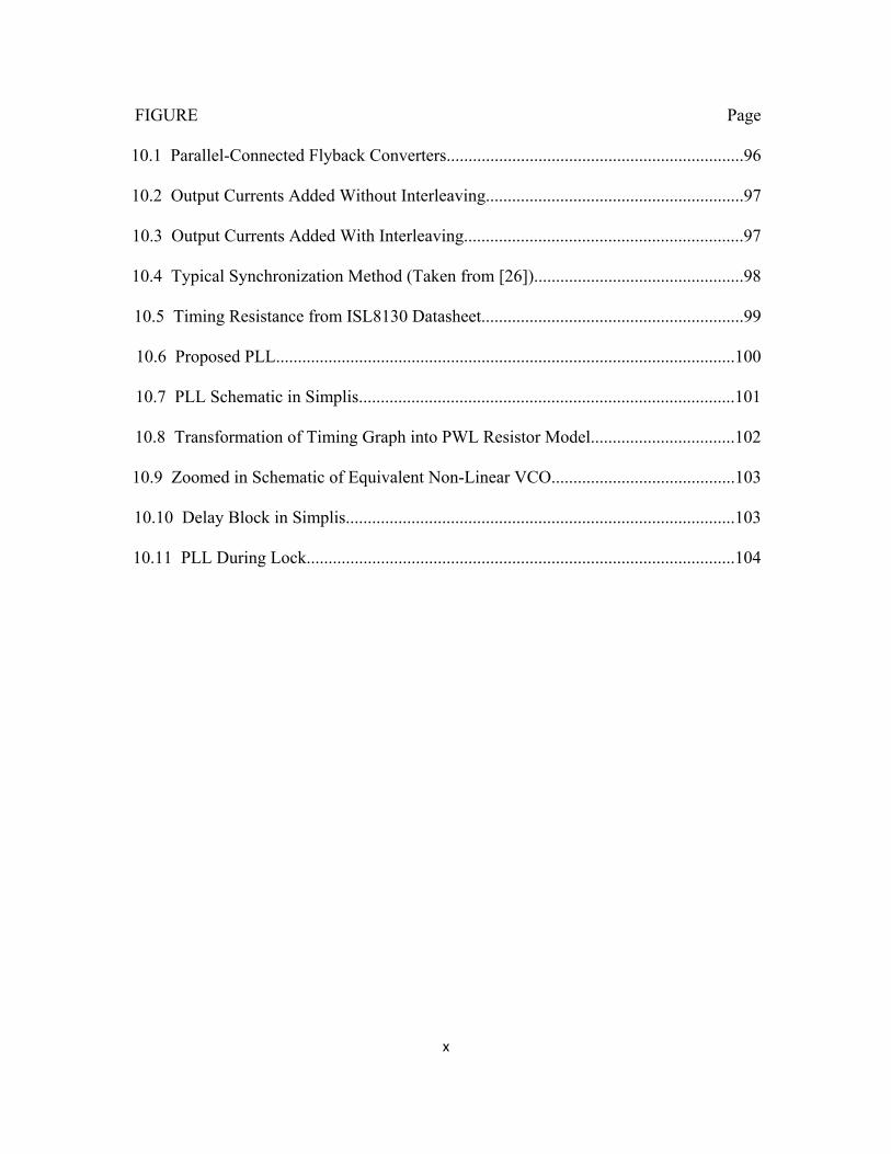
FIGURE Page
10.1 Parallel-Connected Flyback Converters....................................................................96
10.2 Output Currents Added Without Interleaving...........................................................97
10.3 Output Currents Added With Interleaving................................................................97
10.4 Typical Synchronization Method (Taken from [26])................................................98
10.5 Timing Resistance from ISL8130 Datasheet............................................................99
10.6 Proposed PLL.........................................................................................................100
10.7 PLL Schematic in Simplis......................................................................................101
10.8 Transformation of Timing Graph into PWL Resistor Model.................................102
10.9 Zoomed in Schematic of Equivalent Non-Linear VCO..........................................103
10.10 Delay Block in Simplis.........................................................................................103
10.11 PLL During Lock..................................................................................................104
1
CHAPTER 1. INTRODUCTION AND THESIS OUTLINE
1.1 Introduction to Photovoltaic Energy Conversion
Photovoltaic (PV) energy conversion involves direct conversion of sunlight into
electricity. This form of energy conversion, once used primarily for providing power to
remote places such as space satellites, has become a popular source of electric energy for
a variety of reasons. PV is a low-maintenance energy source as it involves no moving
mechanical parts, but the high cost of producing a PV cell had kept PV an impractical
source of energy for many years. Things have changed in recent years, as dropping
production costs for PV cells and modules have coincided with government initiatives to
promote the use of PV. The government initiatives have been a big reason for PV’s
recent proliferation; one example is the U.S. Residential Renewable Energy Tax Credit,
which provides a tax credit in the amount of 30% of the cost of installation [1]. This
boost makes PV a competitive option for power generation; the result has been a massive
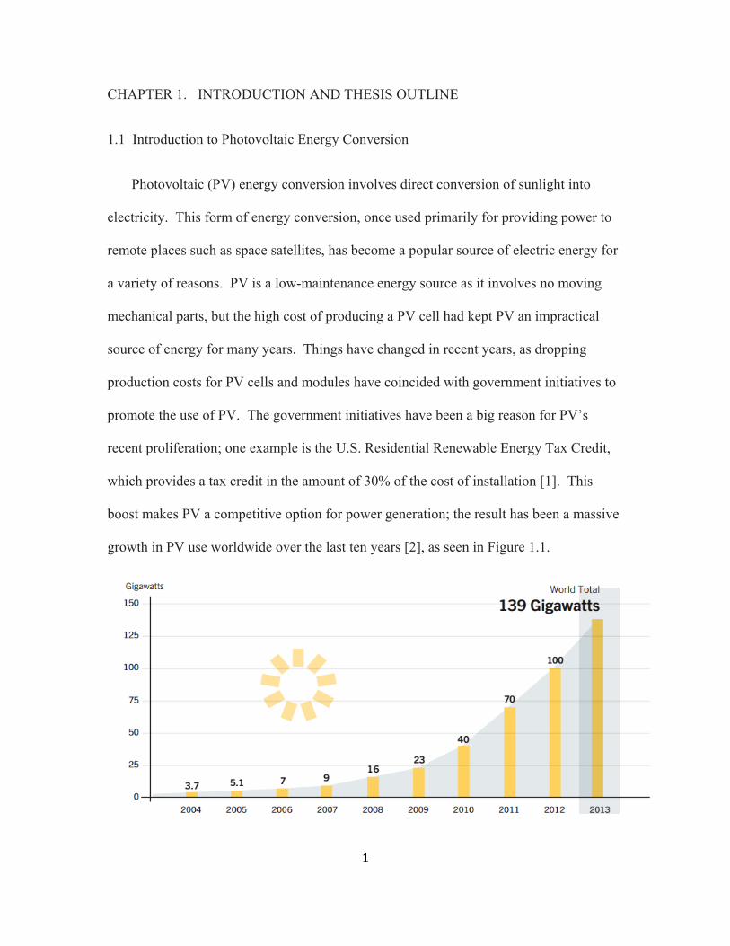
growth in PV use worldwide over the last ten years [2], as seen in Figure 1.1.

2
Figure 1.1 Worldwide PV Capacity (Taken from [2])
The utility sector has seen the most growth. In the United States, California
represents the biggest contributor to the utility sector as it ramps up the use of renewable
energy to meet the California Renewables Portfolio Standard, which states that the
utilities shall have 33% of their retail sales derive from renewable energy sources by the
end of 2020 [3]. Agua Caliente Solar Project, seen in Figure 1.2, has a peak capacity of
290 MW and ships all of this electricity to California from Dateland, AZ.
Figure 1.2 Agua Caliente Solar Project

3
The residential sector has seen tremendous growth as well. Figure 1.3 shows the
PV installations by sector in the United States over the last four years [4].
Figure 1.3 United States PV Installations by Sector (Taken from [4])
Each of the sectors has more installations every single year, and the residential
sector comprises a significant portion of these installations. The fact that there has been
significant growth in the residential sector speaks to the scalability of PV projects, which
can be as small as one rooftop module. Figure 1.4 shows an example of a neighborhood
with a high use of PV.

4
Figure 1.4 Neighborhood with PV Installations
As the PV installations grow in the residential sector, there are more and more
companies competing in the market, and they are developing new methods of installation
to optimize the balance between system cost and system efficiency. In particular, the
architectures for these rooftop systems have been evolving. Central inverters are the
baseline architecture used in commercial-scale and utility-scale PV installations, but are
not commonly used in residential installations. String inverters have been used for many
years in the residential sector, but recently module-level power electronics (MLPE) have
been added to systems to increase the amount of power extracted. MLPE comes in two
flavors: microinverters and DC optimizers. These architectures are shown below in
Figure 1.5.
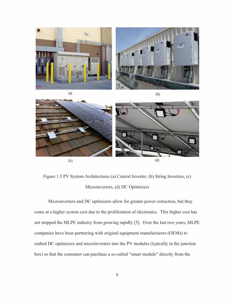
5
Figure 1.5 PV System Architectures (a) Central Inverter, (b) String Inverters, (c)
Microinverters, (d) DC Optimizers
Microinverters and DC optimizers allow for greater power extraction, but they
come at a higher system cost due to the proliferation of electronics. This higher cost has
not stopped the MLPE industry from growing rapidly [5]. Over the last two years, MLPE
companies have been partnering with original equipment manufacturers (OEMs) to
embed DC optimizers and microinverters into the PV modules (typically in the junction
box) so that the consumer can purchase a so-called “smart module” directly from the
6
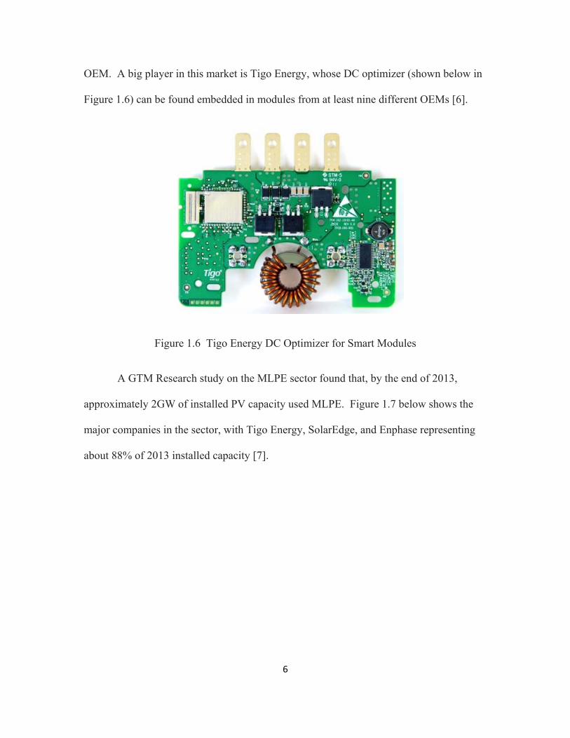
OEM. A big player in this market is Tigo Energy, whose DC optimizer (shown below in
Figure 1.6) can be found embedded in modules from at least nine different OEMs [6].
Figure 1.6 Tigo Energy DC Optimizer for Smart Modules
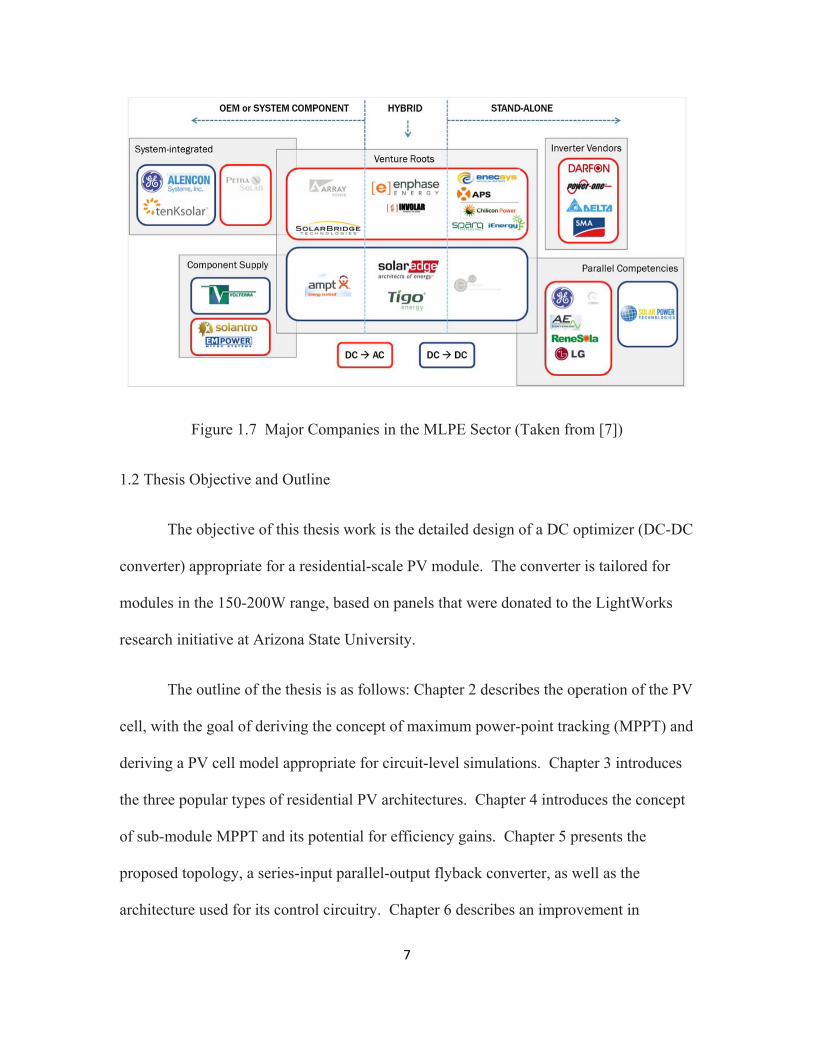
A GTM Research study on the MLPE sector found that, by the end of 2013,
approximately 2GW of installed PV capacity used MLPE. Figure 1.7 below shows the
major companies in the sector, with Tigo Energy, SolarEdge, and Enphase representing
about 88% of 2013 installed capacity [7].
7
Figure 1.7 Major Companies in the MLPE Sector (Taken from [7])
1.2 Thesis Objective and Outline
The objective of this thesis work is the detailed design of a DC optimizer (DC-DC
converter) appropriate for a residential-scale PV module. The converter is tailored for
modules in the 150-200W range, based on panels that were donated to the LightWorks
research initiative at Arizona State University.
The outline of the thesis is as follows: Chapter 2 describes the operation of the PV
cell, with the goal of deriving the concept of maximum power-point tracking (MPPT) and
deriving a PV cell model appropriate for circuit-level simulations. Chapter 3 introduces
the three popular types of residential PV architectures. Chapter 4 introduces the concept
of sub-module MPPT and its potential for efficiency gains. Chapter 5 presents the
proposed topology, a series-input parallel-output flyback converter, as well as the
architecture used for its control circuitry. Chapter 6 describes an improvement in

8
efficiency by using an active clamp technique. Design constraints for the active clamp
circuit are derived for steady-state conditions. Chapter 7 describes the design of the
converter’s gate drive circuitry, which uses gallium-nitride (GaN) FETs to improve
efficiency. Chapter 8 details the complete power stage calculations. Chapter 9 details the
modeling and simulation of the active clamp flyback converter. Chapter 10 describes a
phase-locked loop circuit developed to achieve interleaving in the outputs of the parallel-
connected converters.

9
CHAPTER 2. PV CELL MODELING
2.1 Brief Description of PV Cell Operation
Every semiconductor material has a “bandgap”, which refers to the energy
difference between the valence energy band and conduction energy band. Electrons in
the valence band are attached to nuclei and cannot move freely, while at room
temperature a very small of electrons will be thermally excited to the conduction band
and are free to move about the material [8].
If a photon of light collides with a valence electron, and if the photon has energy
greater than the bandgap, it can transfer its energy to the electron and create an electron-
hole pair. This electron-hole pair will wander briefly and then recombine.
A pn junction is used to separate the electron-hole pair. If the photon transfers its
energy in the vicinity of the pn junction’s depletion region, the electron and hole may
wander into the depletion region and quickly be swept into the n- and p-regions,
respectively. Here they become majority carriers and can contribute to current flow. If
the pn junction, aka diode, is open-circuited, then the majority carrier buildup will lead to
a higher diffusion current. The voltage across the depletion region will grow until the
diffusion and drift currents balance. Conceptually we may think of the light as a current
source, and with no external connection, all of that current is dissipated in the diode, or it
is forward-biased. This is referred to as the open circuit voltage of the PV cell. On the
other hand, if we apply a short across the cell terminals, the drift current will have the
potential to move all the way through the diode to the external wire. In this case, the
voltage across the depletion region will reduce to zero. This is referred to as the short
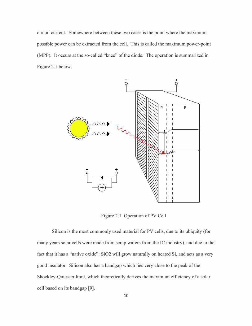
10
circuit current. Somewhere between these two cases is the point where the maximum
possible power can be extracted from the cell. This is called the maximum power-point
(MPP). It occurs at the so-called “knee” of the diode. The operation is summarized in
Figure 2.1 below.
Figure 2.1 Operation of PV Cell
Silicon is the most commonly used material for PV cells, due to its ubiquity (for
many years solar cells were made from scrap wafers from the IC industry), and due to the
fact that it has a “native oxide”: SiO2 will grow naturally on heated Si, and acts as a very
good insulator. Silicon also has a bandgap which lies very close to the peak of the
Shockley-Quiesser limit, which theoretically derives the maximum efficiency of a solar
cell based on its bandgap [9].
11
When photons reach the surface of the semiconductor, they will penetrate a
certain depth before generating an electron-hole pair. Typically, most of the generation
happens very close to the surface, and the rate of generation quickly decays exponentially
into the material [10]. For this reason the pn junction is placed very close to the surface,
on the order of a few micron. Unfortunately, recombination is also highest at the surface.
The dangling bonds of the lattice edge allow electrons to quickly recombine, therefore the
surface is passivated, usually with a layer of SiO2 [11]. As it turns out, the n-type
material is easier to passivate, so the n-type material is placed on top, facing the sun. The
current must flow through metal wires to reach an external circuit, so conductors are
connected to the top and bottom of the cell. The conductors on the top use thin fingers,
as a tradeoff between resistance and blocking sunlight.
2.2 Modeling PV Cell
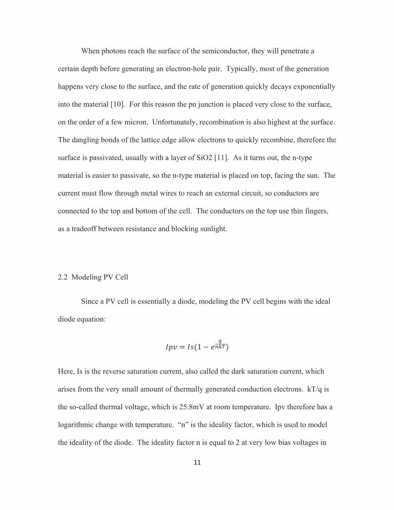
Since a PV cell is essentially a diode, modeling the PV cell begins with the ideal
diode equation:
1
Here, Is is the reverse saturation current, also called the dark saturation current, which
arises from the very small amount of thermally generated conduction electrons. kT/q is
the so-called thermal voltage, which is 25.8mV at room temperature. Ipv therefore has a
logarithmic change with temperature. “n” is the ideality factor, which is used to model
the ideality of the diode. The ideality factor n is equal to 2 at very low bias voltages in

12
the mV range, and it is due to the high-level of generation-recombination current inside
the depletion region at low biases [12]. Since PV cells are always biased near the “knee”
of the diode, we may assume n=1. Apart from the ideal diode equation, each cell has
series resistance, due to the finger connectors and external wiring, and shunt resistance,
which is due to defects in the cell itself. Because the cells are large in area, having some
small defects is an accepted part of their construction [13].
Solar modules were donated to ASU’s LightWorks research group, and their
specifications are shown below in Table 2.1.
Manufacturer Jiawei Baisheng Silicon Solar
Rated power 175W 175W 180W
Voltage @ MPP 36.8V 35.7V 36.2V
Current @ MPP 4.77A 4.9A 4.97A
Open-circuit voltage 44.1V 44V 44.3V
Short-circuit current 5.49A 5.27A 5.76A
Number of cells 72 72 72
Table 2.1 Solar Module Specifications
A figure-of-merit for solar modules is the fill factor (FF), which is the ratio of
maximum power to the product of open-circuit voltage and short-circuit current. For
these panels, we get the following fill factors:
: 36.84.77
44.1 5.49 0.725
13
: 35.74.9
44 5.27 0.754
: 36.24.97
44.3 5.76 0.705
For this thesis work, the Jiawei panel was chosen to model because its FF lies in
the middle of these three panels.
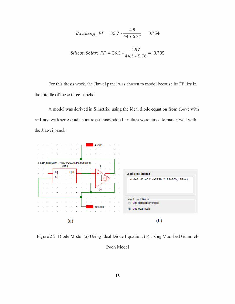
A model was derived in Simetrix, using the ideal diode equation from above with
n=1 and with series and shunt resistances added. Values were tuned to match well with
the Jiawei panel.
Figure 2.2 Diode Model (a) Using Ideal Diode Equation, (b) Using Modified Gummel-
Poon Model
14
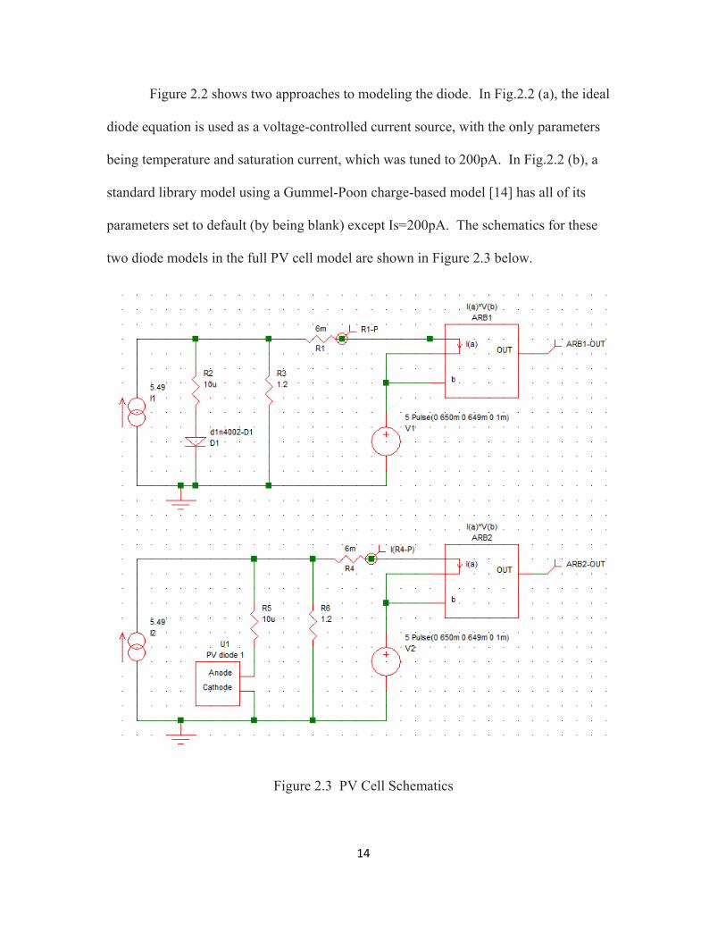
Figure 2.2 shows two approaches to modeling the diode. In Fig.2.2 (a), the ideal
diode equation is used as a voltage-controlled current source, with the only parameters
being temperature and saturation current, which was tuned to 200pA. In Fig.2.2 (b), a
standard library model using a Gummel-Poon charge-based model [14] has all of its
parameters set to default (by being blank) except Is=200pA. The schematics for these
two diode models in the full PV cell model are shown in Figure 2.3 below.
Figure 2.3 PV Cell Schematics
15
Here we can see the tuned values. Isc = 5.49A (per module specifications),
Rseries = 0.006 ohm, Rshunt = 1.2 ohm. Rshunt is a small value which accurately
represents the average defects in the cells, and accounts for the low fill factor of 0.725.
Higher-quality modules (as well as new ones from Jiawei) have fill factors from 0.8 to
0.85.
The voltage sources on the right side of the schematic perform a voltage sweep,
and the boxes calculate the power for plotting. The results of both voltage sweeps are
plotted on top of each other below, to demonstrate the good matching between the
models.
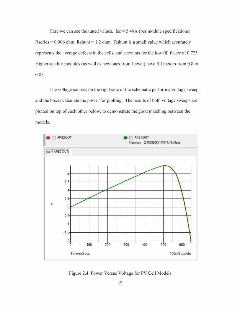
Figure 2.4 Power Versus Voltage for PV Cell Models
16
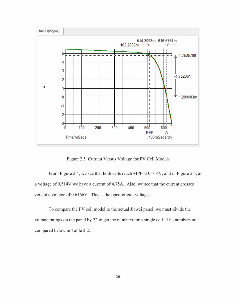
Figure 2.5 Current Versus Voltage for PV Cell Models
From Figure 2.4, we see that both cells reach MPP at 0.514V, and in Figure 2.5, at
a voltage of 0.514V we have a current of 4.75A. Also, we see that the current crosses
zero at a voltage of 0.6166V. This is the open-circuit voltage.
To compare the PV cell model to the actual Jiawei panel, we must divide the
voltage ratings on the panel by 72 to get the numbers for a single cell. The numbers are
compared below in Table 2.2.

17
Jiawei Simetrix model
Isc (input to model) 5.49A 5.49A
Voc 0.613V 0.617V
Imp 4.77A 4.75A
Vmp 0.511V 0.514V
Table 2.2 Comparison of Actual and Modeled PV Values
We see that the models match very well. This can allow us to examine different
operating points of the PV module to better design the conversion circuitry.
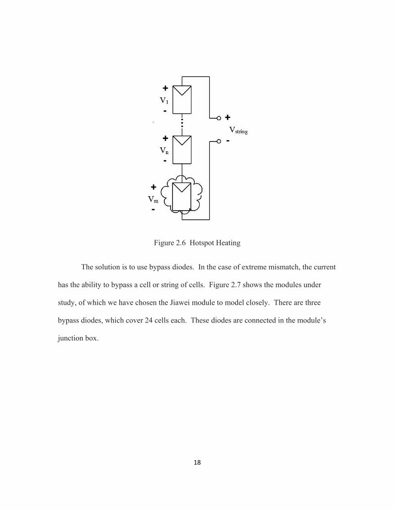
2.3 Bypass Diodes and 72-Cell PV Module
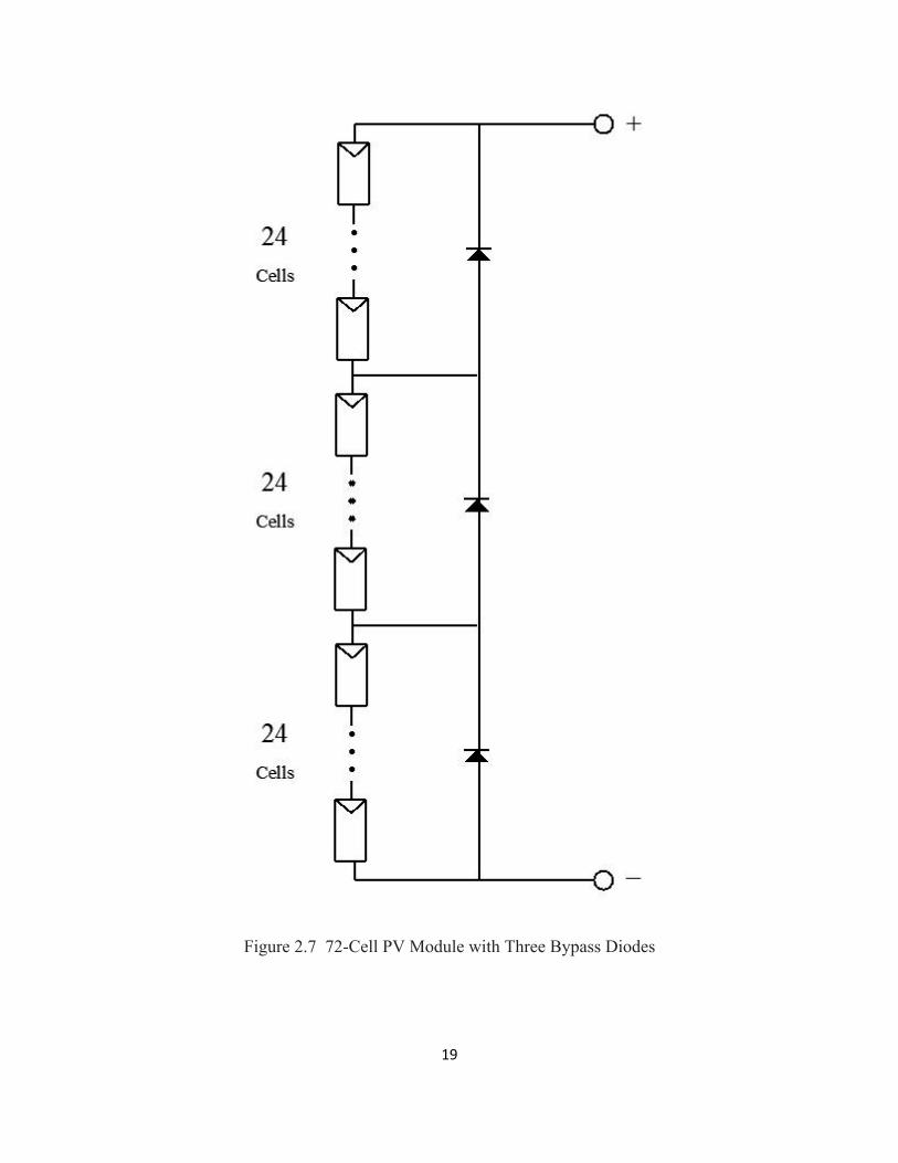
The modules studied in this work are a typical size for residential use, with 72
series cells and three bypass diodes. The bypass diodes are installed for the module’s
safety, to prevent so-called “hotspot heating” in the cells. This condition arises under
mismatch conditions, where one cell is unable to pass current while the other cells are
highly illuminated. If the output voltage is low enough, the shaded cell can reverse bias,
from KVL around the loop. The situation is shown in Figure 2.6. Hotspot heating occurs
when the shaded cell becomes reverse biased and dissipates the energy generated in the
other cells. If the output voltage is held low this can be a problem, as:
1 2
18
Figure 2.6 Hotspot Heating
The solution is to use bypass diodes. In the case of extreme mismatch, the current
has the ability to bypass a cell or string of cells. Figure 2.7 shows the modules under
study, of which we have chosen the Jiawei module to model closely. There are three
bypass diodes, which cover 24 cells each. These diodes are connected in the module’s
junction box.
19
Figure 2.7 72-Cell PV Module with Three Bypass Diodes
20
CHAPTER 3. ARCHITECTURES FOR RESIDENTIAL PV SYSTEMS
3.1 Introduction
In this chapter we discuss the architectures commonly employed for residential
PV systems. Comparing the different architectures is not a simple task, as there are many
factors to balance when designing a PV system, among them cost of installation, cost of
maintenance, system efficiency, solar power extraction, and system reliability. After a
brief comparison of architectures, the DC optimizer architecture is discussed in further
detail to set the appropriate background for the design in this work.
3.2 Common Architectures for Residential PV Systems
3.2.1 Central Inverter
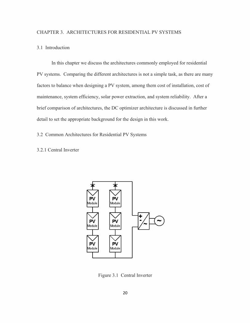
Figure 3.1 Central Inverter
21
Figure 3.1 shows the schematic of a central inverter. They historically have been
used in large installations, where it is convenient to have all of the electronics in one
location. Strings of panels are connected in series to add to large voltages, and these
strings are connected in parallel using blocking diodes as shown in Figure 3.1. Although
central inverters are usually the most practical option for large-scale systems due to the
ease of maintenance, they become less practical as PV systems become smaller, due to
the fact that mismatch in the PV modules can severely restrict power output. Each string
of modules will source the current of its weakest module, and the total system voltage
will be determined by the weakest string. However, if mismatch problems are not
deemed a problem, the central inverter can be a practical solution [15].
3.2.2 String Inverter
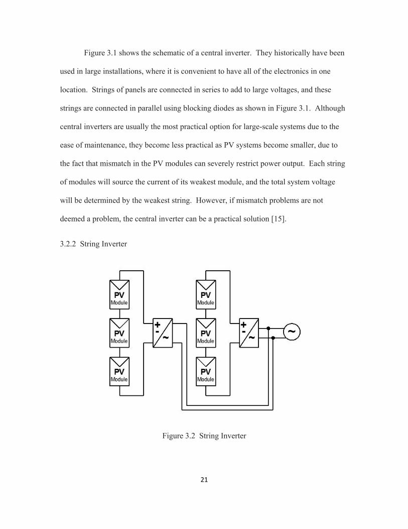
Figure 3.2 String Inverter

22
Figure 3.2 shows the schematic of a pair of string inverters. The string inverter
has historically been the most popular option for residential PV systems, where one
inverter can support a rooftop system on the order of 1-10 kW. MPPT is performed at the
string level, and multiple strings can easily be added in parallel. Similar to central
inverters, the major disadvantage is that mismatch effects within each string will force the
string to either operate at the weakest module’s current, or bypass that module entirely.
Bypass diodes can lead to local power maxima, so global MPPT algorithms must be
implemented [16]-[18].
3.2.3 Microinverter
Figure 3.3 Microinverter
The microinverter architecture, as shown in Figure 3.3, involves using a single
inverter for each PV module. This structure allows for MPPT at the module level, so that
mismatch effects will not affect power extraction of the producing modules. This
architecture is also popular for its plug-and-play flexibility; since each microinverter will
output an AC voltage, a system can use as many or as little modules as desired.
23
Microinverters involve a lot of electronics—the most of any PV architecture. For this
reason, initial costs for a system are higher. Moreover, maintenance can be costly, as the
microinverters can be hard to access once installed.
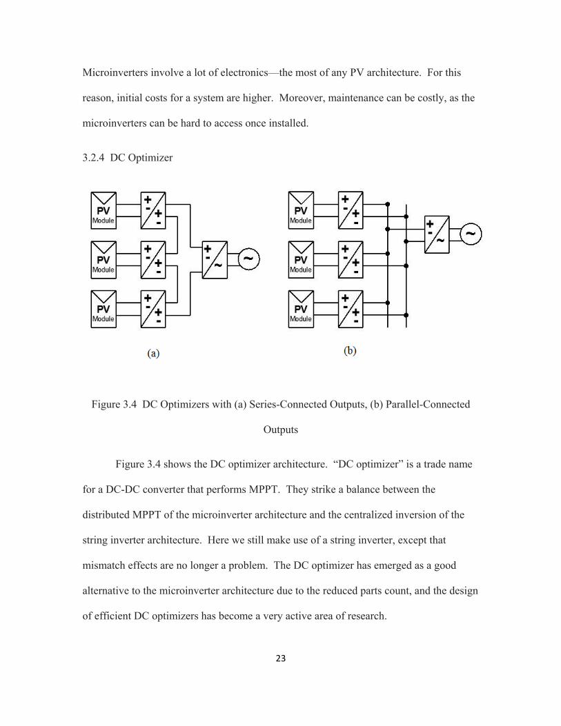
3.2.4 DC Optimizer
Figure 3.4 DC Optimizers with (a) Series-Connected Outputs, (b) Parallel-Connected
Outputs
Figure 3.4 shows the DC optimizer architecture. “DC optimizer” is a trade name
for a DC-DC converter that performs MPPT. They strike a balance between the
distributed MPPT of the microinverter architecture and the centralized inversion of the
string inverter architecture. Here we still make use of a string inverter, except that
mismatch effects are no longer a problem. The DC optimizer has emerged as a good
alternative to the microinverter architecture due to the reduced parts count, and the design
of efficient DC optimizers has become a very active area of research.
24
3.3 Recent Developments in DC Optimizers
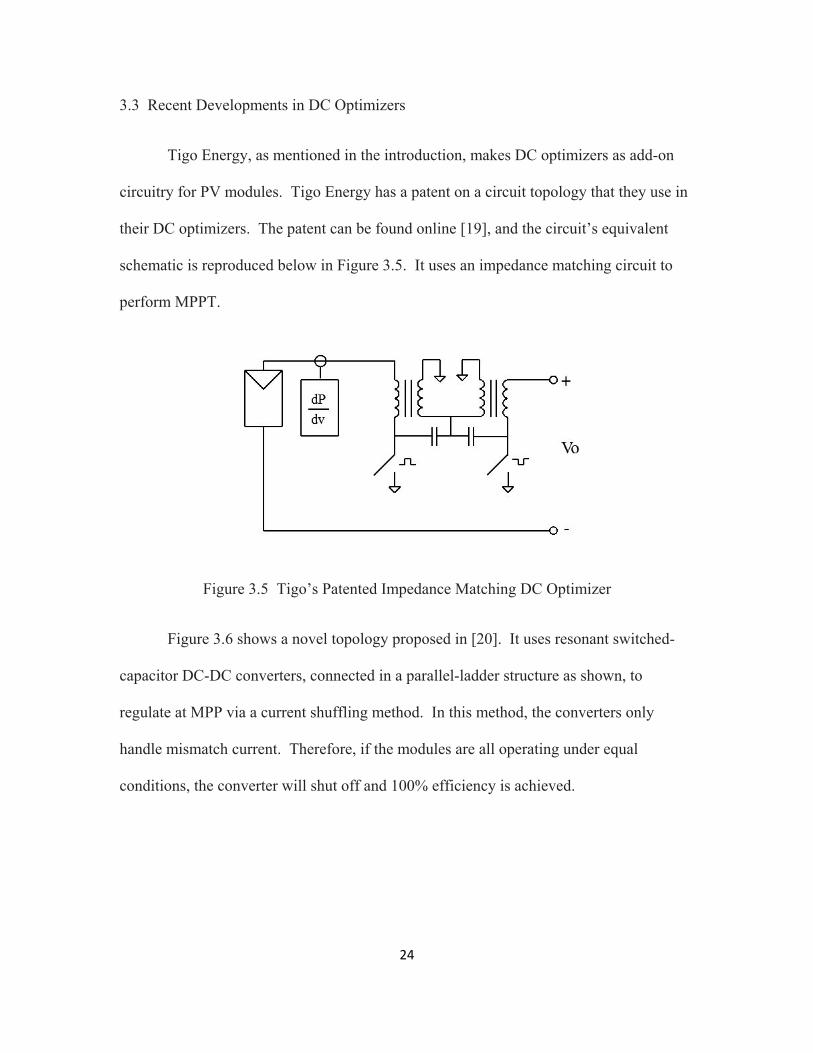
Tigo Energy, as mentioned in the introduction, makes DC optimizers as add-on
circuitry for PV modules. Tigo Energy has a patent on a circuit topology that they use in
their DC optimizers. The patent can be found online [19], and the circuit’s equivalent
schematic is reproduced below in Figure 3.5. It uses an impedance matching circuit to
perform MPPT.
Figure 3.5 Tigo’s Patented Impedance Matching DC Optimizer
Figure 3.6 shows a novel topology proposed in [20]. It uses resonant switched-
capacitor DC-DC converters, connected in a parallel-ladder structure as shown, to
regulate at MPP via a current shuffling method. In this method, the converters only
handle mismatch current. Therefore, if the modules are all operating under equal
conditions, the converter will shut off and 100% efficiency is achieved.
25
Figure 3.6 Parallel-Ladder Current-Shuffling DC Optimizer
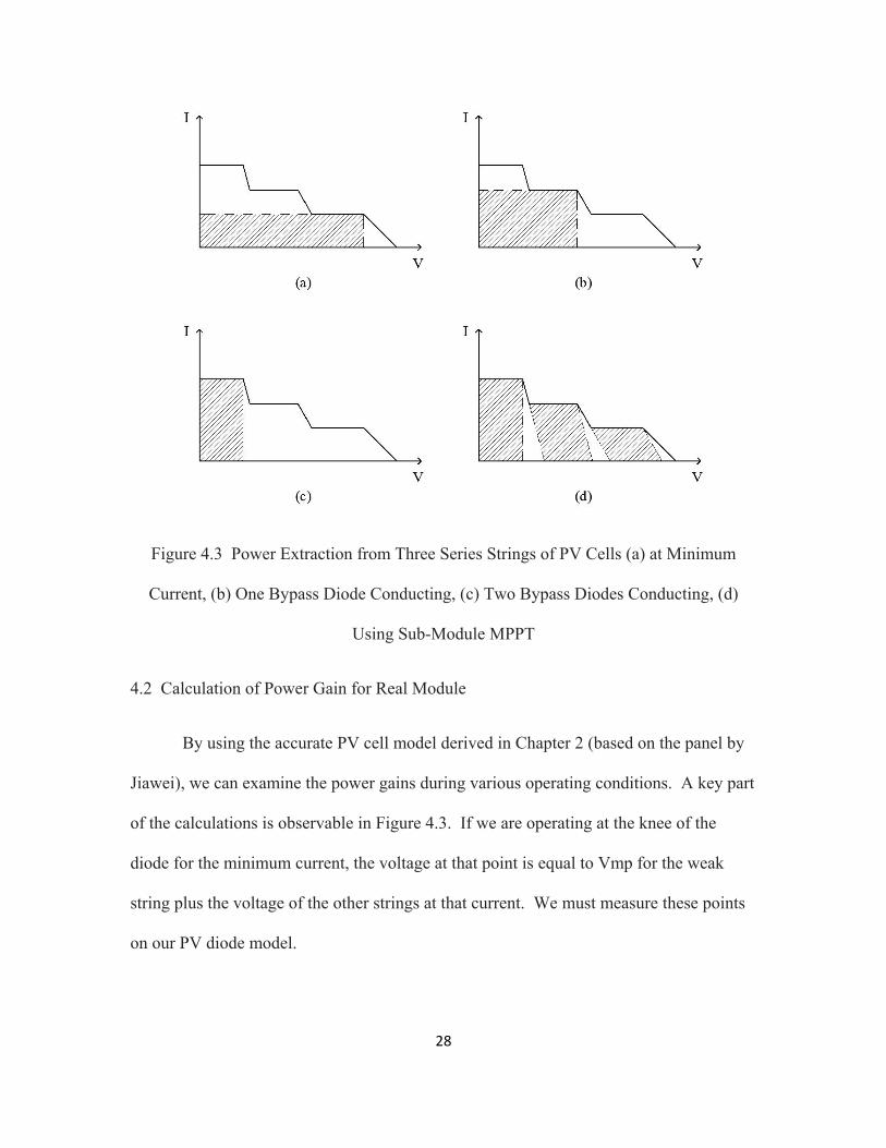
In [21], the approach taken is to maximize cost and efficiency of the DC-DC
converters, and they propose using cheap and efficient synchronous buck converters and
achieving voltage gain by using series-connected modules. The miniature design is
shown in Figure 3.7 below.
Figure 3.7 Synchronous Buck Converters at Sub-Module Level

26
CHAPTER 4. SUB-MODULE MPPT
4.1 Introduction to Sub-Module MPPT
The last two circuits mentioned in Chapter 3 make use of sub-module MPPT,
which is a growing trend among new DC optimizers. Sub-module MPPT involves
performing DC-DC conversion on portions of the cells in a DC module. With current
module construction, there are typically four electrical connections to the cells, and the
bypass diodes are connected there. Therefore the connections can be used to place three
DC-DC converters. To convert at a finer scale would require changes to PV module
construction. To understand sub-module conversion, it helps to consider the V/I curve
for series cells using the simplified diode model. In Figure 4.1, two strings of PV cells
with different short circuit current levels are connected in series. The series connection
means that we add the values on the V/I plots horizontally.
Figure 4.1 Using Simplified Diode Model to Visualize Mismatch of Series Cells
With this simplified model, local MPP maxima occur at the “knees” of the simplified
diodes. If we imagine that the module has no bypass diodes, the converter will regulate
at the local MPP of the smaller current. Having a bypass diode gives the option of

27
regulating at the other local maximum, at the knee of the higher current. With sub-
module more power is extracted, as shown in Figure 4.2.
Figure 4.2 Power Extraction from Two Series Strings of PV Cells with (a) Minimum
Current, (b) Use of Bypass Diode, (c) Sub-Module MPPT
With sub-module MPPT we can extract the power represented by the areas in
Figure 4.2 (c). Not only to we gain power extraction using this method, but the MPPT
algorithm can be simplified, as there is no longer a need to search for a global maximum.
The local maximum is the global maximum for a single string of cells.
The situation in our case is three series strings of PV cells, and in this case the
typical MPPT algorithm will have up to three local maxima to choose from, depending on
how many bypass diodes are conducting. Sub-module MPPT avoids this problem while
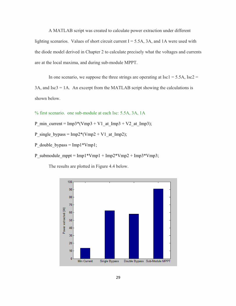
extracting power from all three segments, as shown in Figure 4.3.
28
Figure 4.3 Power Extraction from Three Series Strings of PV Cells (a) at Minimum
Current, (b) One Bypass Diode Conducting, (c) Two Bypass Diodes Conducting, (d)
Using Sub-Module MPPT
4.2 Calculation of Power Gain for Real Module
By using the accurate PV cell model derived in Chapter 2 (based on the panel by
Jiawei), we can examine the power gains during various operating conditions. A key part
of the calculations is observable in Figure 4.3. If we are operating at the knee of the
diode for the minimum current, the voltage at that point is equal to Vmp for the weak
string plus the voltage of the other strings at that current. We must measure these points
on our PV diode model.
29
A MATLAB script was created to calculate power extraction under different
lighting scenarios. Values of short circuit current I = 5.5A, 3A, and 1A were used with
the diode model derived in Chapter 2 to calculate precisely what the voltages and currents
are at the local maxima, and during sub-module MPPT.
In one scenario, we suppose the three strings are operating at Isc1 = 5.5A, Isc2 =
3A, and Isc3 = 1A. An excerpt from the MATLAB script showing the calculations is
shown below.
% first scenario. one sub-module at each Isc: 5.5A, 3A, 1A
P_min_current = Imp3*(Vmp3 + V1_at_Imp3 + V2_at_Imp3);
P_single_bypass = Imp2*(Vmp2 + V1_at_Imp2);
P_double_bypass = Imp1*Vmp1;
P_submodule_mppt = Imp1*Vmp1 + Imp2*Vmp2 + Imp3*Vmp3;
The results are plotted in Figure 4.4 below.

30
Figure 4.4 Power Extraction During Mismatch Scenario 1
In the next scenario, we let Isc1 = 5.5A, Isc2 = Isc3 = 1A.
An excerpt from the MATLAB script is shown below.
% second scenario. one sub-module at Isc = 5.5V, the others at 1A
P_min_current2 = Imp3*(Vmp3 + Vmp3 + V1_at_Imp3);
P_double_bypass2 = Imp1*Vmp1;
P_submodule_mppt2 = Imp1*Vmp1 + 2*Imp3*Vmp3;
The results are shown below in Figure 4.5 (note that there is one less local
maximum due to Isc2 and Isc3 being equal).
Figure 4.5 Power Extraction During Mismatch Scenario 2

31
In scenario 2, the double bypass power is close to the sub-module MPPT power
due to the fact that two of the strings are sourcing very little power, and bypassing them
gains almost all the power. This is a useful tool for analyzing power gains with sub-
module MPPT, but its accuracy is limited by the accuracy of the PV diode model used.
32
CHAPTER 5. PROPOSED DC OPTIMIZER AND CONTROL ARCHITECTURE
5.1 Proposed DC Optimizer
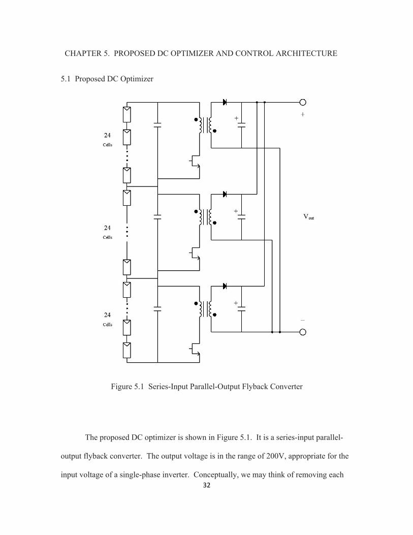
Figure 5.1 Series-Input Parallel-Output Flyback Converter
The proposed DC optimizer is shown in Figure 5.1. It is a series-input parallel-
output flyback converter. The output voltage is in the range of 200V, appropriate for the
input voltage of a single-phase inverter. Conceptually, we may think of removing each

33
bypass diode from the original module and replacing it with a flyback converter, and then
placing the outputs of these flyback converters in parallel. In the following sections we
discuss the derivation of the converter and its advantages over a typical DC optimizer.
5.2 Derivation of Proposed Converter
5.2.1 Input Capacitors
As we have seen, the voltage/current characteristics of a PV cell (or string of
cells) approach those of a DC current source. We desire to maintain the cells operating at
or near their MPP, but if we attach a DC-DC converter to the cells’ terminals, we can
expect to draw discontinuous currents from the cells, or currents with large amounts of
ripple. During segments of the switching period where input current is zero, the cells are
briefly open circuited, and the PV current will be absorbed in the cells as it forward
biases the diodes.
What we desire is to decouple the DC PV power from the switching action of the
DC-DC converter. The solution is to use large capacitors, which will supply the
discontinuous and/or ripple current to the converter, while allowing the DC current to
flow from the cells. If the capacitors are large enough, the voltage across the cells’
terminals will stay roughly constant over a switching period. Essentially, this converts a
current source to a voltage source, from which we can theoretically use any well-known
DC-DC converter.
For a properly rated capacitor, there is no danger of overvoltage conditions, due to
the fact that the cells can only supply current up to their Voc limit. If the DC-DC
34
converter is shut off during daylight conditions, the PV current source will continue to
charge the capacitors until Voc is reached, when all of the current will then flow through
the PV diodes. Therefore the value of Voc can be used to select the voltage rating of the
capacitors.
5.2.2 Necessity for Isolation
As a first attempt to select an appropriate DC-DC converter, we may consider
using a simple boost converter, as we will be stepping up the PV voltage to 200V. This
leads to a huge problem, as shown below in Figure 5.2.
Figure 5.2 Input Voltage Shorted to (a) Output Voltage, (b) Ground
Here we see the result of stacking two boost converters. The problem comes from
the fact that the inputs are connected together. In Fig. 5.2 (a), the outputs of the
converters are connected in series. This leads to the input voltage of the lower converter
being shorted to its own output, as a result of the ground node of the upper converter. In
Fig. 5.2 (b), the outputs are connected in parallel. Here the result is different but equally
devastating, as the upper converter’s ground node shorts the lower converter’s input to
35
ground. This problem does not exist in the typical DC optimizer scheme, where there is
one converter per module, and nothing forcing us to connect together the inputs of the
modules.
This same problem exists for all of the major non-isolated DC-DC converters, due
to the existence of the ground node. This forces us to use transformer isolation.
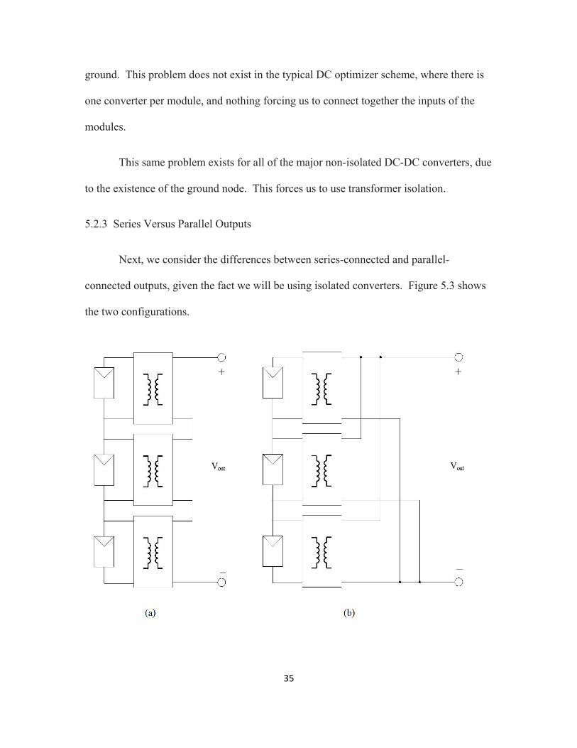
5.2.3 Series Versus Parallel Outputs
Next, we consider the differences between series-connected and parallel-
connected outputs, given the fact we will be using isolated converters. Figure 5.3 shows
the two configurations.

36
Figure 5.3 Series-Input Isolated Converters with (a) Series-Connected Outputs, (b)
Parallel-Connected Outputs
These two options both solve the problem encountered with non-isolated
converters. For the series-connected converters, the output voltages sum to 200V, and
the output currents are all equal. For the parallel-connected converters, the output
voltages are all equal to 200V, and the output currents sum to equal Iout for the whole
converter. At first glance, the series-connected configuration might seem better due to
the smaller turns ratio. The input voltages will be in the 12V range, and in the parallel
case they will be stepped up to 200V, where in the series-connected case, the voltages
will ideally be stepped up to 200V/3 = 67V. A smaller turns ratio will improve
efficiency, but there are some problems with the series-connected output configuration
which makes it less attractive in this application.
5.2.4 Problems with Series-Connected Outputs
Using series-connected outputs is advantageous when all converters are operating
under similar lighting conditions. However, we are using sub-module conversion in
order to gain power output, so we must consider cases where there are mismatch effects.
For example, consider a case where sub-module 1 receives full sunlight, with Imp = 5A,
Vmp = 12V, and the other two modules receive much less sunlight, on the order of Imp =
1A, Vmp = 11V. We can calculate the output voltage of converter 1 as follows:
5 12 1 11 1 11 82

37
82200
410
1 5120.41
146.3
We see that under mismatch conditions, the converter with more power will be
forced to regulate at a much higher output voltage than under ideal conditions. In the
extreme case of two converters being completely cut off from sunlight, one converter will
regulate at the full output voltage of 200V. Each converter must be designed to regulate
over a very wide range. This will lead to the converters having a much smaller duty ratio
at the ideal operating point where Vout = 67V.
There is another problem with using series-connected outputs for this application.
When sunlight is low, the converters will eventually turn off. It is desirable, for the
purpose of maximum power extraction, that the converters be able to turn on and off
independently. If one converter is receiving sunlight, we would like to receive power
from it, regardless of the other converters. However, we encounter a problem when one
converter turns off. It is explained in Figure 5.4.
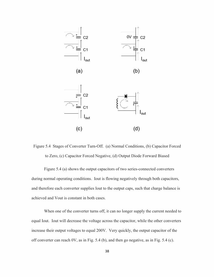
38
Figure 5.4 Stages of Converter Turn-Off. (a) Normal Conditions, (b) Capacitor Forced
to Zero, (c) Capacitor Forced Negative, (d) Output Diode Forward Biased
Figure 5.4 (a) shows the output capacitors of two series-connected converters
during normal operating conditions. Iout is flowing negatively through both capacitors,
and therefore each converter supplies Iout to the output caps, such that charge balance is
achieved and Vout is constant in both cases.
When one of the converter turns off, it can no longer supply the current needed to
equal Iout. Iout will decrease the voltage across the capacitor, while the other converters
increase their output voltages to equal 200V. Very quickly, the output capacitor of the
off converter can reach 0V, as in Fig. 5.4 (b), and then go negative, as in Fig. 5.4 (c).

39
Once the capacitor reaches a voltage of -0.7V, it will forward bias the converter’s output
diode, as seen in Fig. 5.4 (d) (shown here is a flyback converter, but a forward converter
will see the same effect). Conduction of the diode may or may not be a problem, but it is
certainly a problem for the capacitor to swing negative, as this limits the type of capacitor
that can be used. Electrolytics and tantalums cannot be used during this condition. The
alternative is to force all converters to shut down as soon as a minimum voltage is
reached by any of the output capacitors. This will greatly restrict the range of conditions
over which the DC optimizer is useful.
Given the preceding discussion, the parallel-output topology is chosen for this
design. All that remains is to choose an isolated converter. The flyback converter is
appropriate for this design based on the requirements for high output voltage and low
output current, and its low parts count will help to minimize cost.
5.3 Effect on System
The parallel-output converter can be hooked directly to the input of an inverter.
The ground of the output capacitor will then be tied to the inverter’s input ground.
Additionally, other optimizers can be connected in parallel, as shown in Figure 5.5. The
total number of parallel converters is only limited by the capacity of the inverter.
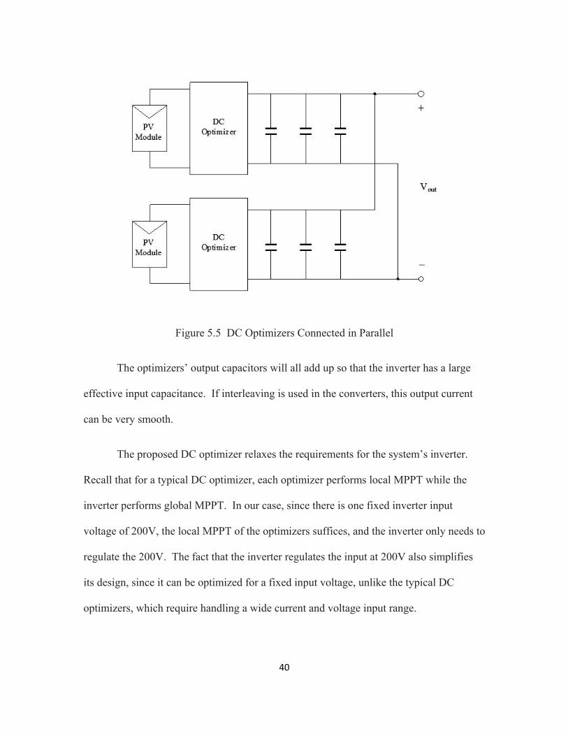
40
Figure 5.5 DC Optimizers Connected in Parallel
The optimizers’ output capacitors will all add up so that the inverter has a large
effective input capacitance. If interleaving is used in the converters, this output current
can be very smooth.
The proposed DC optimizer relaxes the requirements for the system’s inverter.
Recall that for a typical DC optimizer, each optimizer performs local MPPT while the
inverter performs global MPPT. In our case, since there is one fixed inverter input
voltage of 200V, the local MPPT of the optimizers suffices, and the inverter only needs to
regulate the 200V. The fact that the inverter regulates the input at 200V also simplifies
its design, since it can be optimized for a fixed input voltage, unlike the typical DC
optimizers, which require handling a wide current and voltage input range.
41
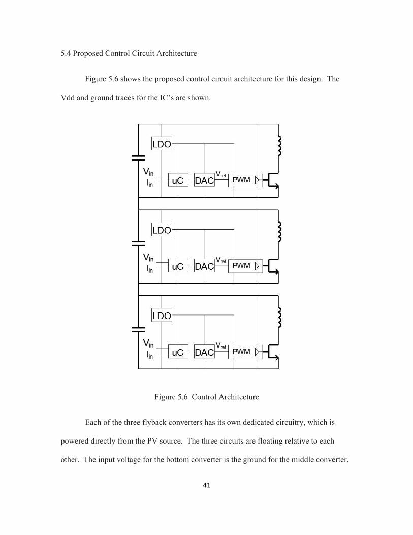
5.4 Proposed Control Circuit Architecture
Figure 5.6 shows the proposed control circuit architecture for this design. The
Vdd and ground traces for the IC’s are shown.
Figure 5.6 Control Architecture
Each of the three flyback converters has its own dedicated circuitry, which is
powered directly from the PV source. The three circuits are floating relative to each
other. The input voltage for the bottom converter is the ground for the middle converter,
42
and so on. By using local control, we eliminate the need for isolated signal lines and
floating/bootstrap gate drivers.
The microcontroller performs voltage and current measurement, and executes the MPPT
algorithm. There are many microcontrollers suitable for this application, and the choice
should be based on cost. Ideally the microcontroller would have just enough memory to
hold the algorithm. Here we assume that the microcontroller contains an ADC as well.
Once a new value of PV voltage is chosen by the algorithm, the microcontroller sends
this value to a DAC which converts it to an analog voltage on the Vref pin of the PWM
controller. The PWM controller performs voltage-mode control based on the value of
Vref, and the value of Vin (feedback pin not shown in the above schematic). The gate
driver (included in the PWM IC in the above schematic) supplies current to the gate of
the FET. The gate driver is a heavier power dissipator than the other IC’s, and by using
the PV voltage to directly supply the gate driver, the LDO size can be minimized, and
voltage dips on the LDO output can be minimized. By connecting the gate driver to the
PV voltage, we will drive the FET harder as power levels increase. It is a nice
coincidence in this case that the PV voltage (6-14V) is the perfect range to drive a typical
power MOSFET.
The LDO linear regulator provides power to all of the IC’s. Some LDO IC’s have
the option to add undervoltage lockout (UVLO) by adding a couple resistors, and we take
full advantage of that feature here. By using UVLO on the PV voltage, we can choose at
what light intensity level the converter will turn on and off. The idea is for the converter
to naturally turn on and off with the sun, with no need for external control.

43
Figure 5.7 Using UVLO to Turn On/Off Converter with Sunlight
The daily cycle is as follows, as illustrated in Figure 5.7. Before sunrise, the
converter is off, and as the sun rises, the PV cells will start to conduct while the converter
is still turned off. Therefore the module will be operating at Voc. At a certain Voc
determined by the UVLO circuit (point A), the converter will turn on. The MPPT
algorithm will search for the MPP (point B), which will be a lower voltage than Voc.
The voltage can decrease, and the UVLO circuitry will prevent the converter from
shutting off. The circuit will continue to operate under all normal light conditions (point
C). As the sunlight is waning, the MPP voltage will eventually start to drop. When the
MPP voltage reaches the lower limit of the UVLO circuit, the converter will turn off
(point D). Because there is always a little bit of light, the cells will return to Voc after
being turned off (point E). Therefore the UVLO values must be chosen such that the

44
converter turns off at a lower light intensity than where the converter turns on (point E <
point B), otherwise the converter could enter a hiccup mode at turn off, where the
converter reaches its UVLO threshold, turns off, the cell voltages increase to Voc, the
converter turns on, decreases to MPP, and so on. In chapter 8 we will choose values for
the UVLO circuit as we perform the power stage calculations.
45
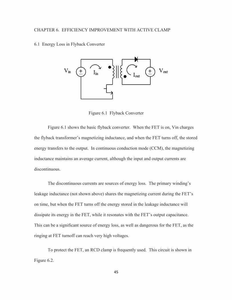
CHAPTER 6. EFFICIENCY IMPROVEMENT WITH ACTIVE CLAMP
6.1 Energy Loss in Flyback Converter
Figure 6.1 Flyback Converter
Figure 6.1 shows the basic flyback converter. When the FET is on, Vin charges
the flyback transformer’s magnetizing inductance, and when the FET turns off, the stored
energy transfers to the output. In continuous conduction mode (CCM), the magnetizing
inductance maintains an average current, although the input and output currents are
discontinuous.
The discontinuous currents are sources of energy loss. The primary winding’s
leakage inductance (not shown above) shares the magnetizing current during the FET’s
on time, but when the FET turns off the energy stored in the leakage inductance will
dissipate its energy in the FET, while it resonates with the FET’s output capacitance.
This can be a significant source of energy loss, as well as dangerous for the FET, as the
ringing at FET turnoff can reach very high voltages.
To protect the FET, an RCD clamp is frequently used. This circuit is shown in
Figure 6.2.
46
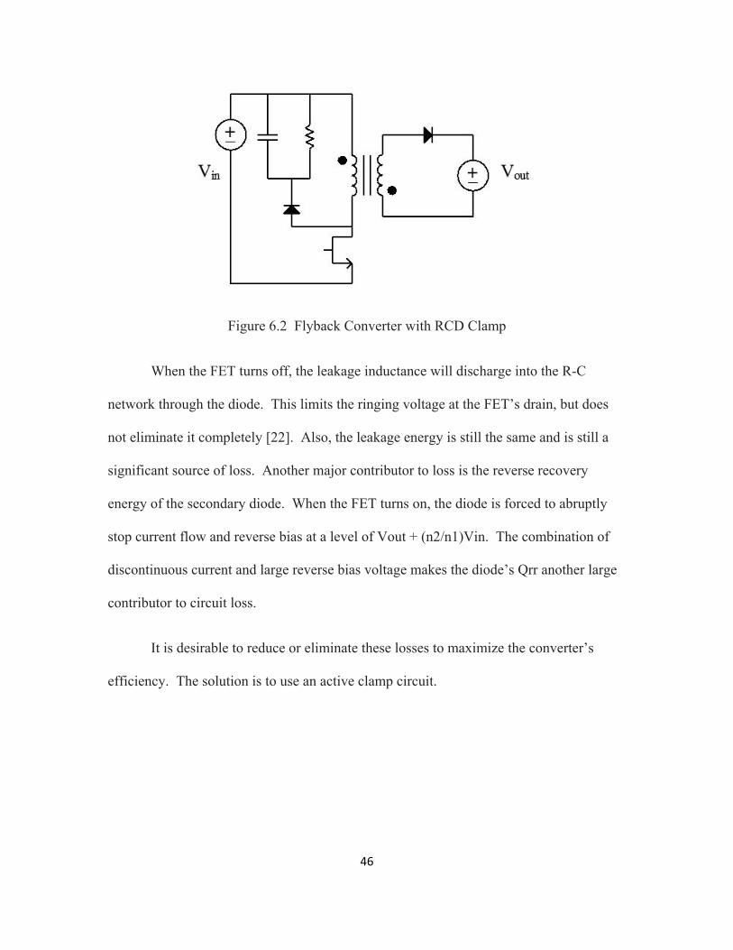
Figure 6.2 Flyback Converter with RCD Clamp
When the FET turns off, the leakage inductance will discharge into the R-C
network through the diode. This limits the ringing voltage at the FET’s drain, but does
not eliminate it completely [22]. Also, the leakage energy is still the same and is still a
significant source of loss. Another major contributor to loss is the reverse recovery
energy of the secondary diode. When the FET turns on, the diode is forced to abruptly
stop current flow and reverse bias at a level of Vout + (n2/n1)Vin. The combination of
discontinuous current and large reverse bias voltage makes the diode’s Qrr another large
contributor to circuit loss.
It is desirable to reduce or eliminate these losses to maximize the converter’s
efficiency. The solution is to use an active clamp circuit.
47
Figure 6.3 Active Clamp Flyback Converter with (a) High-Side Clamp, (b) Low-Side
Clamp
Figure 6.3 shows the addition of an active clamp to the flyback converter. Here
the magnetizing inductance Lm and leakage inductance Llk are explicitly shown. The
operation of the circuit is the same for the high-side and low-side configurations. There
are a few subtle differences between the two converters, which we will discuss in a later
section. The differences will lead us to choose the high-side active clamp for this
application.
6.2 Steady-State Operation of Active Clamp Flyback Converter
In this section we describe the steady-state operation of the active clamp flyback
converter. The switching period can be described as seven different segments. The
switching waveforms are shown below in Figure 6.4, which is adapted from [23].
48
Figure 6.4 Active Clamp Flyback Waveforms (adapted from [23])
49
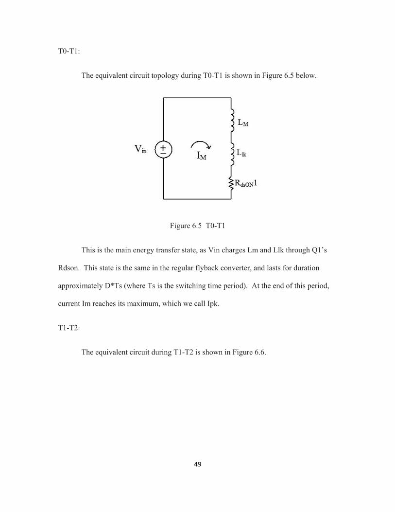
T0-T1:
The equivalent circuit topology during T0-T1 is shown in Figure 6.5 below.
Figure 6.5 T0-T1
This is the main energy transfer state, as Vin charges Lm and Llk through Q1’s
Rdson. This state is the same in the regular flyback converter, and lasts for duration
approximately D*Ts (where Ts is the switching time period). At the end of this period,
current Im reaches its maximum, which we call Ipk.
T1-T2:
The equivalent circuit during T1-T2 is shown in Figure 6.6.
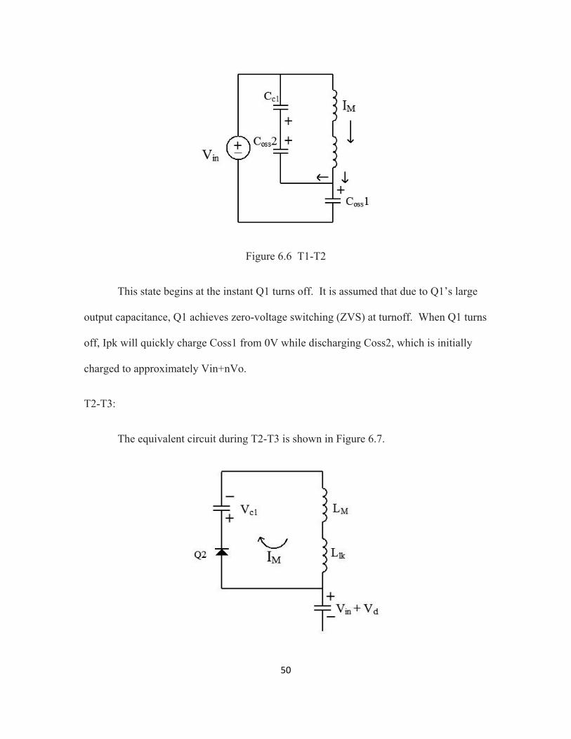
50
Figure 6.6 T1-T2
This state begins at the instant Q1 turns off. It is assumed that due to Q1’s large
output capacitance, Q1 achieves zero-voltage switching (ZVS) at turnoff. When Q1 turns
off, Ipk will quickly charge Coss1 from 0V while discharging Coss2, which is initially
charged to approximately Vin+nVo.
T2-T3:
The equivalent circuit during T2-T3 is shown in Figure 6.7.
51
Figure 6.7 T2-T3
Ipk charges Coss1 and discharges Coss2 until Coss2 reaches -0.7V and its diode
conducts. This marks the instant T2. During the brief interval T2-T3, current is almost
constant at Ipk. The resonance between Lm and Vcl is much too slow to play a role here.
Since Q2’s diode is conducting, Q2 may turn on after T2 with ZVS.
T3-T4:
The equivalent circuit during T3-T4 is shown in Figure 6.8.
Figure 6.8 T3-T4
At T3, Vcl has increased enough such that V(Lm) reaches –nVo, and becomes
clamped there. This marks the beginning of the resonant period, as Llk resonates with
Ccl. Ilk initially charges Ccl, but becomes negative around halfway through this time
interval. Initially, Ilk = Im = Ipk, so the output current begins ramping up from zero,
instead of the abrupt edge as in the regular flyback. As Ilk decreases, more of the
magnetizing current goes to the output. When Ilk becomes negative, both the
magnetizing and leakage currents flow to the output. Therefore Iout has a peak level
52
higher, almost double, than the regular flyback. Note that the deadtime between Q1
turning off and Q2 turning on is flexible, as Q2 has until Ilk changes direction to turn on
with ZVS.
T4-T5:
The equivalent circuit during T4-T5 is shown in Figure 6.9.
Figure 6.9 T4-T5
At T4, Q2 turns off. Ilk has reached its negative peak, and this current discharges
Coss1 while charging Coss2. The energy stored in Coss1 is delivered to the output. This
is a brief time interval, governed by the time constant from Llk and (Coss1 || Coss2). For
Q1 to achieve ZVS, Llk must have enough energy to completely discharge Coss1 and
charge Coss2. In the event that Llk cannot completely discharge Coss1, Q1 should turn
on at the minimum voltage possible. We will have more to say about this when we
derive design constraints for the converter.
53
T5-T6:
The equivalent circuit during T5-T6 is shown in Figure 6.10.
Figure 6.10 T5-T6
Once Ilk has completely discharged Coss1, and reaches -0.7V, Q1’s body diode
will conduct. Q1 can turn on with ZVS during this interval. The leakage current decays
at a constant rate, due to being clamped at Vin+nVo. The output current, equal to
n(Im+Ilk), decays as well.
T6-T7:
The equivalent circuit during T6-T7 is shown in Figure 6.11.
54
Figure 6.11 T6-T7
Q1 is on and leakage current becomes positive again. The voltage across the
magnetizing inductor remains clamped at –nVo while the output current ramps down at a
rate due to Llk. This soft decay will reduce the effect of reverse recovery once Iout
becomes zero at T7. At T7, leakage current equals magnetizing current and we start the
cycle again.
6.3 Derivation of Design Constraints
We mentioned that T2 begins when Q2’s body diode forward conducts. This
situation is shown again in Figure 6.12 (a), with an alternative scenario in Figure 6.12 (b).
55
Figure 6.12 Events at T2. (a) Diode Conducts First, (b) Vm Clamped at –nVo First
As Coss1 increases and Coss2 decreases, the diode will conduct before Vm is
clamped to –nVo, but why? We know that Vcl is roughly equal to nVo, so the answer is
not obvious. The alternative scenario in Figure 6.12 (b) shows what happens if Vm
becomes clamped to –nVo first. Ipk will continue to charge Coss1 and discharge Coss2,
but with a very fast resonant time segment, due to the capacitances Coss1 and Coss2, and
leakage inductance Llk. This brief resonant period will increase the noise of the circuit
and the RMS current losses. It is desired to avoid this scenario. This leads us to the first
design constraint. For Q2’s body diode to conduct first, the ratio of leakage inductances
must be constrained to the following:
0.7
Another design constraint arises at T4, which is shown again below for
convenience.
56
Figure 6.13 State of the Circuit at T4
We will derive the design constraint to achieve ZVS on Q1, by comparing the energy in
Coss1 and Coss2 to the energy contained in Llk at Q2 turnoff.
We know that the initial energy in Llk is given by:
12
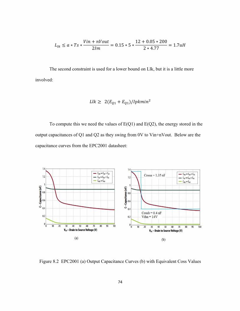
However, calculating the energy in Coss1 and Coss2 is not as simple, because FET
output capacitance is non-linear over voltage, and we are completely discharging Coss1
(and completely charging Coss2) during this interval. If we use the value of capacitance
at Vin+nVo, we could be quite a bit off of the actual value. Some typical Coss versus
voltage curves are shown in Figure 6.14.
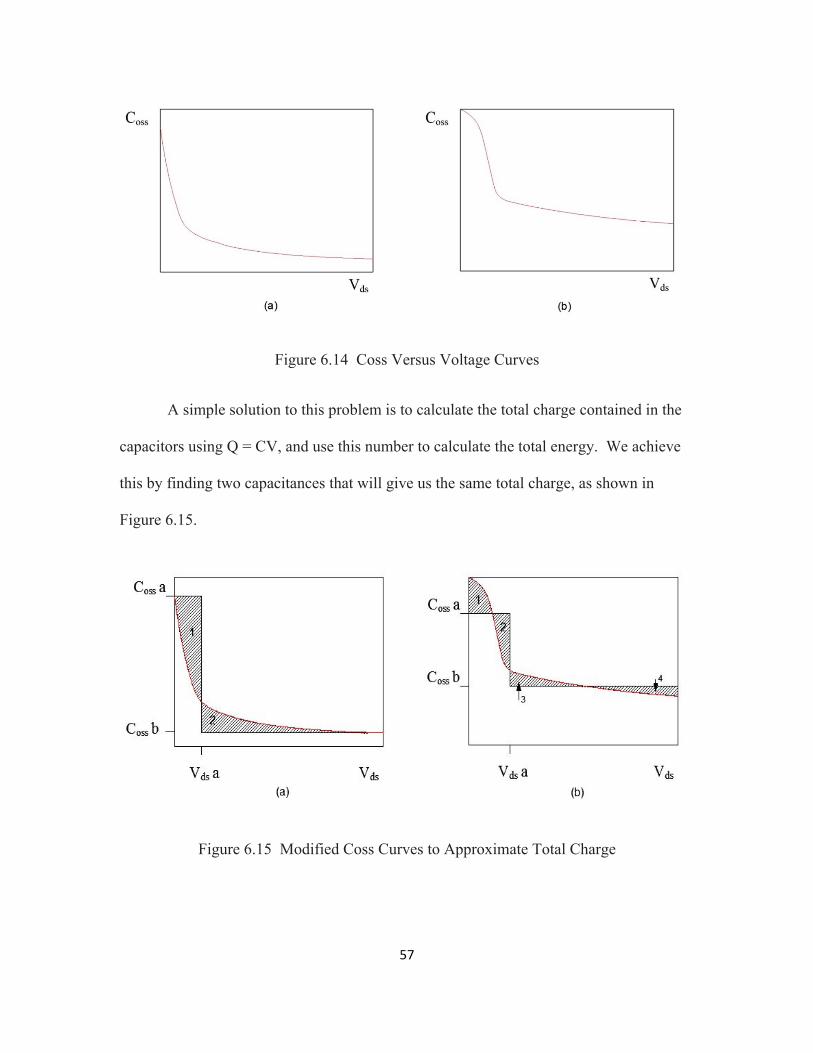
57
Figure 6.14 Coss Versus Voltage Curves
A simple solution to this problem is to calculate the total charge contained in the
capacitors using Q = CV, and use this number to calculate the total energy. We achieve
this by finding two capacitances that will give us the same total charge, as shown in
Figure 6.15.
Figure 6.15 Modified Coss Curves to Approximate Total Charge

58
We use this square approximation, knowing that the total charge is the area under
the curve from 0V to Vin+nVo. We choose two values, Cossa and Cossb, such that the
following hold:
Area 1 = Area 2 (for curves such as 6.15 (a))
Area 1 + Area 3 = Area 2 + Area 4 (for curves such as 6.15 (b))
To calculate the energy, we start by calculating total charge, which is the area
underneath the straight lines:
Then we use this to find the equivalent capacitance at a given value of Vds.
This gives us the energy in Coss:
12
12 1
2
12
Now we are ready for the design constraint, which is that the minimum leakage
inductance energy be greater or equal to the total Coss energy:
2 /
59
The next design constraint is regarding the length of time between T4 and T7.
During this time the output current is decaying and the leakage current is returning to
equalling the magnetizing current. This time interval decreases the effective duty of the
converter, and although the slower decay of output current will reduce reverse recovery,
we should keep this interval to some minimum percentage of Ts. Figure 6.16, taken from
[24] shows how we can simplify to three time intervals, with the interval in question
lasting time a*Ts.
Figure 6.16 Simplification into Three Time Intervals (Taken from [24])
The slope during (0,aTs) is determined by the input and output across the leakage
inductance. We will choose a maximum value for “a” which leads to a constraint on Llk:
2
The final design constraint is regarding deadtime between Q2 turnoff and Q1
turnon. Because deadtime is something we cannot change, we must turnon Q1 when Vds

60
reaches its minimum. In the event that there is not enough energy to forward bias the
diode, this deadtime will minimize energy loss.
The minimum will occur at ¼ the resonant time period between Llk and (Coss1 ||
Coss2).
2
6.4 Stability of Clamp Voltage
An assumption has been implicitly made about the voltage across the clamp
capacitor. Looking at the waveform for Vcl in Figure 6.4, we notice that Vcl always
peaks in the middle of the resonant period, and returns to its initial value. It is constant
over a switching cycle. Consider the fact that Llk and Ccl have a given resonant
frequency, with a given period. Since the duty in our converter can vary over a
moderately wide range, how do we know Vcl will always return to its original value? If,
at the beginning of the resonant period, Ilk is at the peak of a cosine waveform, then Vcl
will be at the middle of a sine wave, and will only return to its initial value if the duty is
exactly half of the resonant period. Clearly this cannot be the case.
As it turns out, when the resonant period begins and Ilk = Ipk, the current begins
between the peak of a cosine and the zero crossing. The peak of the cosine then
corresponds to all of the energy being contained in Llk, and none of it in Ccl (here we
refer to the differential voltage across Ccl with respect to nVo). For a given duty, the
converter will quickly stabilize such that the following hold:

61
1. Clamp capacitor voltage peaks at the middle of the resonant interval
2. Leakage inductor current crosses zero at the middle of the resonant interval
3. Leakage inductor current begins the resonant interval at Ipk, and ends the resonant
interval at –Ipk
The only necessary condition is that the resonant interval (Q1 off time) be less
than half of the resonant period due to Ccl and Llk:
A MATLAB script was written to verify this analysis, which proves to be too
cumbersome to prove in a closed form.
Figures 6.17 and 6.18 show the results of the MATLAB script.
62
Figure 6.17 Convergence of Phase to be Centered around pi/2
In Figure 6.17, for various lengths of Toff with respect to the resonant period, we
calculate and plot the phase difference between the center of the interval and the pi/2
point on the cosine (current) and sine (voltage) waves, over sequential cycles. Here we
see that they rapidly converge, verifying the plot of Vcl in Figure 6.4.
Figure 6.18 Clamp Voltage Stabilizing
Figure 6.18 shows the stabilization of the clamp voltage (actually voltage
difference to nVo) over sequential cycles. This convergence implies that any off time
will be stable in the converter, as long as the maximum off time is less than half the
resonant frequency (although oscillations take more time to settle when Toff approaches
half the resonant frequency).

63
Since we have shown that the leakage inductor crosses zero at the middle of the
resonant interval (middle of the main FET’s off time), we can use this result to calculate
the steady-state voltage of the clamp capacitor. Specifically, we will calculate the
difference between the clamp capacitor voltage and nVo. This additional clamp voltage
can be used for another design constraint, specifically minimum off time, or maximum
duty, as the clamp voltage will grow larger with smaller off times.
We use the fact that the initial energy in the clamp capacitor and leakage inductor
is the total energy in the resonant circuit, and define Imax to be the peak of the cosine,
where all of the energy has transferred to the inductor:
cos 2
When the cosine reaches Im, the time is as follows:
2√ 1 /2
We use this time to calculate Imax, and use Imax to calculate ∆Vcl:
/cos 2
1
2√
∆
This can be used to balance the tradeoff between maximum duty and clamp
capacitor voltage.

64
6.5 Summary of Design Constraints
Our derived design constraints are collected below in Table 6.1.
Constraint Notes
0.7
Eliminate resonance between Llk
and Coss
2 /
ZVS on Q1 over operating range
2
Limits effective duty
2
FETs turn on at minimum voltage
Stability of clamp voltage
∆
High duty increases clamp voltage
Table 6.1 Summary of Design Constraints
65
CHAPTER 7. EFFICIENCY IMPROVEMENT WITH GAN FETS
7.1 Introduction
Gallium Nitride (GaN) has in recent years become a popular material for making
FETs. First used for RF transistors, GaN-on-Si devices exhibit a unique property of a 2-
dimensional electron gas (2DEG) which allows electrons to flow at a very high
conductance. In the last ten years, the attractive 2DEG property led researchers to try to
develop FETs appropriate for power conversion. The first company to sell GaN FETs for
power conversion applications is Efficient Power Conversion (EPC), a company founded
by Alex Lidow, former CEO of International Rectifier. The GaN FETs sold by EPC
(called eGaN FETs) used a recessed gate structure to block the 2DEG until the gate
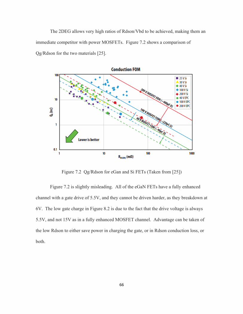
voltage goes high, creating a normally-off FET. Figure 7.1 shows the structure of a
lateral silicon MOSFET alongside the eGaN FET. The structures are very similar, where
the 2DEG acts as the channel.
Figure 7.1 Structure of (a) Lateral Si MOSFET, (b) eGaN FET
66
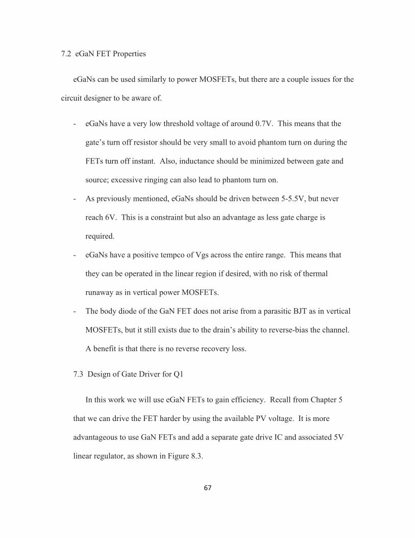
The 2DEG allows very high ratios of Rdson/Vbd to be achieved, making them an
immediate competitor with power MOSFETs. Figure 7.2 shows a comparison of
Qg/Rdson for the two materials [25].
Figure 7.2 Qg/Rdson for eGan and Si FETs (Taken from [25])
Figure 7.2 is slightly misleading. All of the eGaN FETs have a fully enhanced
channel with a gate drive of 5.5V, and they cannot be driven harder, as they breakdown at
6V. The low gate charge in Figure 8.2 is due to the fact that the drive voltage is always
5.5V, and not 15V as in a fully enhanced MOSFET channel. Advantage can be taken of
the low Rdson to either save power in charging the gate, or in Rdson conduction loss, or
both.
67
7.2 eGaN FET Properties
eGaNs can be used similarly to power MOSFETs, but there are a couple issues for the
circuit designer to be aware of.
- eGaNs have a very low threshold voltage of around 0.7V. This means that the
gate’s turn off resistor should be very small to avoid phantom turn on during the
FETs turn off instant. Also, inductance should be minimized between gate and
source; excessive ringing can also lead to phantom turn on.
- As previously mentioned, eGaNs should be driven between 5-5.5V, but never
reach 6V. This is a constraint but also an advantage as less gate charge is
required.
- eGaNs have a positive tempco of Vgs across the entire range. This means that
they can be operated in the linear region if desired, with no risk of thermal
runaway as in vertical power MOSFETs.
- The body diode of the GaN FET does not arise from a parasitic BJT as in vertical
MOSFETs, but it still exists due to the drain’s ability to reverse-bias the channel.
A benefit is that there is no reverse recovery loss.
7.3 Design of Gate Driver for Q1
In this work we will use eGaN FETs to gain efficiency. Recall from Chapter 5
that we can drive the FET harder by using the available PV voltage. It is more
advantageous to use GaN FETs and add a separate gate drive IC and associated 5V
linear regulator, as shown in Figure 8.3.
68
Figure 7.3 Gate Driver (a) for MOSFET (b) for GaN FET
The LM5113 is a gate drive IC designed specifically for driving GaN FETs,
providing separate outputs for the on current and off current, so that resistance can be
optionally added for the on path, and not for the off path. We can quickly calculate
the gained efficiency for this new configuration:
Figure 7.4 Driving a MOSFET (a) On, (b) Off
Figure 7.4 shows the current paths for driving a MOSFET from the PV voltage.
During turn on, Ron will dissipate 1/2CV^2 joules and during turn off, Roff will
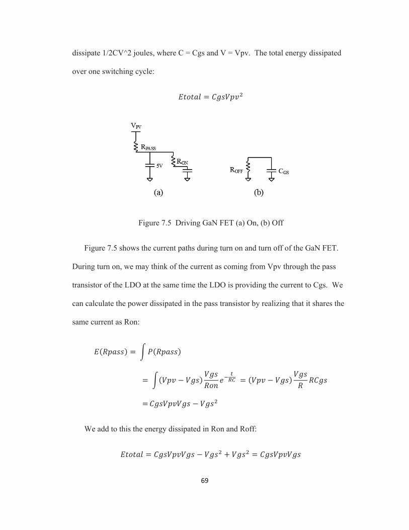
69
dissipate 1/2CV^2 joules, where C = Cgs and V = Vpv. The total energy dissipated
over one switching cycle:
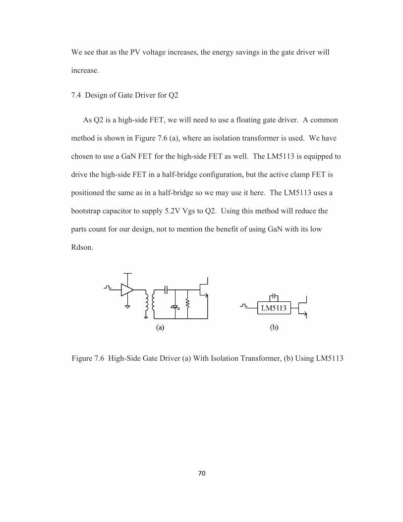
Figure 7.5 Driving GaN FET (a) On, (b) Off
Figure 7.5 shows the current paths during turn on and turn off of the GaN FET.
During turn on, we may think of the current as coming from Vpv through the pass
transistor of the LDO at the same time the LDO is providing the current to Cgs. We
can calculate the power dissipated in the pass transistor by realizing that it shares the
same current as Ron:
We add to this the energy dissipated in Ron and Roff:
70
We see that as the PV voltage increases, the energy savings in the gate driver will
increase.
7.4 Design of Gate Driver for Q2
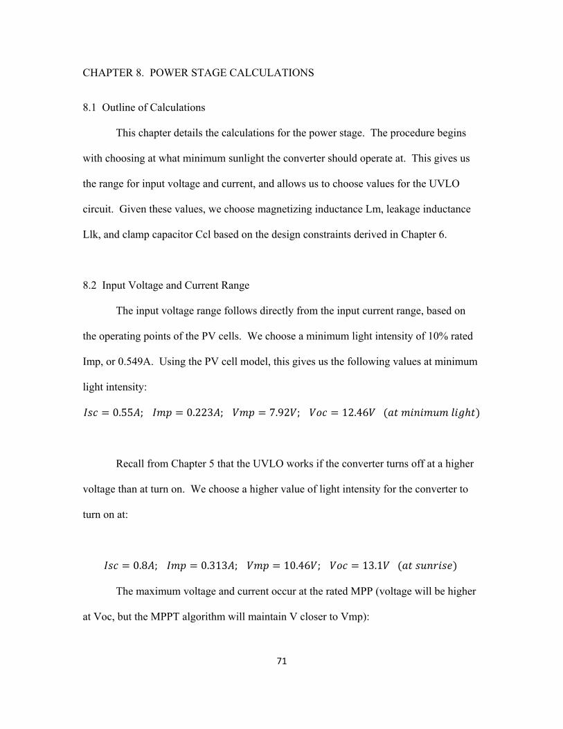
As Q2 is a high-side FET, we will need to use a floating gate driver. A common
method is shown in Figure 7.6 (a), where an isolation transformer is used. We have
chosen to use a GaN FET for the high-side FET as well. The LM5113 is equipped to
drive the high-side FET in a half-bridge configuration, but the active clamp FET is
positioned the same as in a half-bridge so we may use it here. The LM5113 uses a
bootstrap capacitor to supply 5.2V Vgs to Q2. Using this method will reduce the
parts count for our design, not to mention the benefit of using GaN with its low
Rdson.
Figure 7.6 High-Side Gate Driver (a) With Isolation Transformer, (b) Using LM5113
71
CHAPTER 8. POWER STAGE CALCULATIONS
8.1 Outline of Calculations
This chapter details the calculations for the power stage. The procedure begins
with choosing at what minimum sunlight the converter should operate at. This gives us
the range for input voltage and current, and allows us to choose values for the UVLO
circuit. Given these values, we choose magnetizing inductance Lm, leakage inductance
Llk, and clamp capacitor Ccl based on the design constraints derived in Chapter 6.
8.2 Input Voltage and Current Range
The input voltage range follows directly from the input current range, based on
the operating points of the PV cells. We choose a minimum light intensity of 10% rated
Imp, or 0.549A. Using the PV cell model, this gives us the following values at minimum
light intensity:
0.55 ; 0.223 ; 7.92 ; 12.46
Recall from Chapter 5 that the UVLO works if the converter turns off at a higher
voltage than at turn on. We choose a higher value of light intensity for the converter to
turn on at:
0.8 ; 0.313 ; 10.46 ; 13.1
The maximum voltage and current occur at the rated MPP (voltage will be higher
at Voc, but the MPPT algorithm will maintain V closer to Vmp):

72
5.49 ; 4.77 ; 12.27 ; 14.7
The converter should be designed to operate at currents as high as Isc and
voltages as high as Voc, if not for safety then for derating of the converter. This gives us
the range for input voltage and current:
: 7.92 14.7 ; : 0.223 5.49
8.3 Choice of Switching Frequency, Duty and Turns Ratio
The switching frequency is chosen to be fs = 200kHz, a good tradeoff between
size and switching losses.
The tradeoff between duty and turns ratio for most DC-DC converters will be
optimum at around d=0.5, which balances RMS currents on the primary and secondary
and the voltage stress on the primary MOSFET. In our case, the input voltage varies over
a small range as power varies over a wide range. It is desirable to have as wide a range of
duty as possible, to increase the resolution of the MPPT algorithm. To this end, we plot
the range of duty versus turns ratio n in MATLAB, using the flyback converter equation:
1
1 ;
12
The plots below in Figure 8.1 show how duty varies with n, at maximum input
voltage, minimum input voltage, and MPP voltage. (note that Dmax in the figure refers
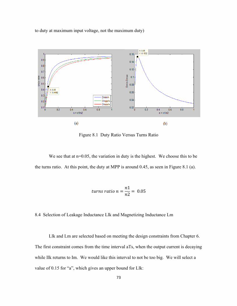
73
to duty at maximum input voltage, not the maximum duty)
Figure 8.1 Duty Ratio Versus Turns Ratio
We see that at n=0.05, the variation in duty is the highest. We choose this to be
the turns ratio. At this point, the duty at MPP is around 0.45, as seen in Figure 8.1 (a).
12
0.05
8.4 Selection of Leakage Inductance Llk and Magnetizing Inductance Lm
Llk and Lm are selected based on meeting the design constraints from Chapter 6.
The first constraint comes from the time interval aTs, when the output current is decaying
while Ilk returns to Im. We would like this interval to not be too big. We will select a
value of 0.15 for “a”, which gives an upper bound for Llk:
74
20.15 5
12 0.05 2002 4.77
1.7
The second constraint is used for a lower bound on Llk, but it is a little more
involved:
2 /
To compute this we need the values of E(Q1) and E(Q2), the energy stored in the
output capacitances of Q1 and Q2 as they swing from 0V to Vin+nVout. Below are the
capacitance curves from the EPC2001 datasheet:
Figure 8.2 EPC2001 (a) Output Capacitance Curves (b) with Equivalent Coss Values

75
We use the approximation derived in Chapter 6 to calculate E(Q1) and E(Q2) as
they swing from 0V to Vin+nVout:
212
Plugging the values in from Figure 8.2 (b),
14 1.35 0.4 24 0.4 24
549
We may now use the above formula for the design constraint:
2
25490.223
22
This constraint will be unwieldy, just for achieving ZVS at minimum input
current. If we look at the lower bound given previously as 1.7uH, we can see at what
minimum current we will achieve ZVS:
1.7 : 2 / 2 5491.7
0.80

76
Since 0.80A is sufficiently low, we can consider 1.7uH to be a good estimate for
Llk. We choose a round value of Llk = 2uH:
2
Lm is selected based on Llk using the following design constraint:
0.7
0.7 0.05 200 2/0.7 28.6
We choose Lm = 27uH. Using a standard value component can give potential to
use an off-the-shelf part (although not optimized for efficiency). As a check, we can use
this value of Lm to look at the magnetizing current ripple at MPP:
∆12.2627
0.45 5 1.02
The magnetizing current at MPP is:
4.770.45
10.6
Therefore the ripple represents 1.02/10.6 = 9.6% change in current. This will reduce
RMS current losses versus the usual accepted value of 20% current ripple.

77
8.5 Selection of Ccl
In general, Ccl should be large as to minimize its voltage swings during the
resonant interval. A strict lower bound comes from the design constraint:
Plugging in our value of Llk=2uH,
0.558 51.7
45.2
To approximate the voltage swing on Ccl during the resonant period, we note that
the leakage current Ilk will roughly follow a sawtooth waveform from Ipk to 0 in the first
half of the resonant interval. Therefore we can measure the voltage ripple on Ccl by
looking at the charge delivered from Llk:
∆14
For Ccl=68uF, at MPP we have:
∆14
4.770.55 54 68
48
Since the steady-state voltage across Vcl is nVo = 10V, a ripple of 48mV is acceptable.

78
Therefore we choose Ccl = 68uF.
The remaining components will be chosen in the following chapter as we perform
open-loop simulations to verify the converter’s operation.

79
CHAPTER 9. MODELING AND SIMULATION OF ACTIVE CLAMP FLYBACK
9.1 Discussion on Modeling and Simulation
In this section, we will model the various components of the flyback converter
and put them together to perform simulations of the converter. Simulation of power
electronics converters is not trivial, as it involves capturing circuit behavior for widely
ranging time constants. We would like to observe switching behavior as well as low-
frequency transient behavior. We will use Simplis as the circuit simulator for this
section. Simplis and Simetrix are packaged together, and use the same schematic entry
GUI, but Simetrix is a SPICE-based simulator whereas Simplis is specifically made for
switching circuits such as power converters. Simplis uses piecewise-linear (PWL)
models to approximate the behavior of circuit elements. This approximation allows for
faster simulation times. In the following sections, we will develop PWL models for the
PV sub-module and for the GaN FET. We will use simplified models for the flyback
transformer and PWM IC to perform open-loop simulations which accurately depict the
switching behavior of the circuit.
9.2 PWL Model of PV Sub-Module
We will begin by modeling the string of 24 PV cells. In Chapter 2, we used
Simetrix to develop a very accurate PV cell model, based on the module made by Jiawei.
We can place 24 of these cells in series in Simetrix, and by measuring various points on
the V-I curve we describe the sub-module as a PWL resistor. We adjust the value of Isc

80
to extract PWL models at any desired illumination level. The 24-cell schematic is shown
in Figure 9.1.
Figure 9.1 24 Series Cells in Simetrix
The circuit on the right of the schematic performs a voltage sweep of the cells and
measures current and power. The current waveform for the case of Isc=5.49 is shown in
Figure 9.2.
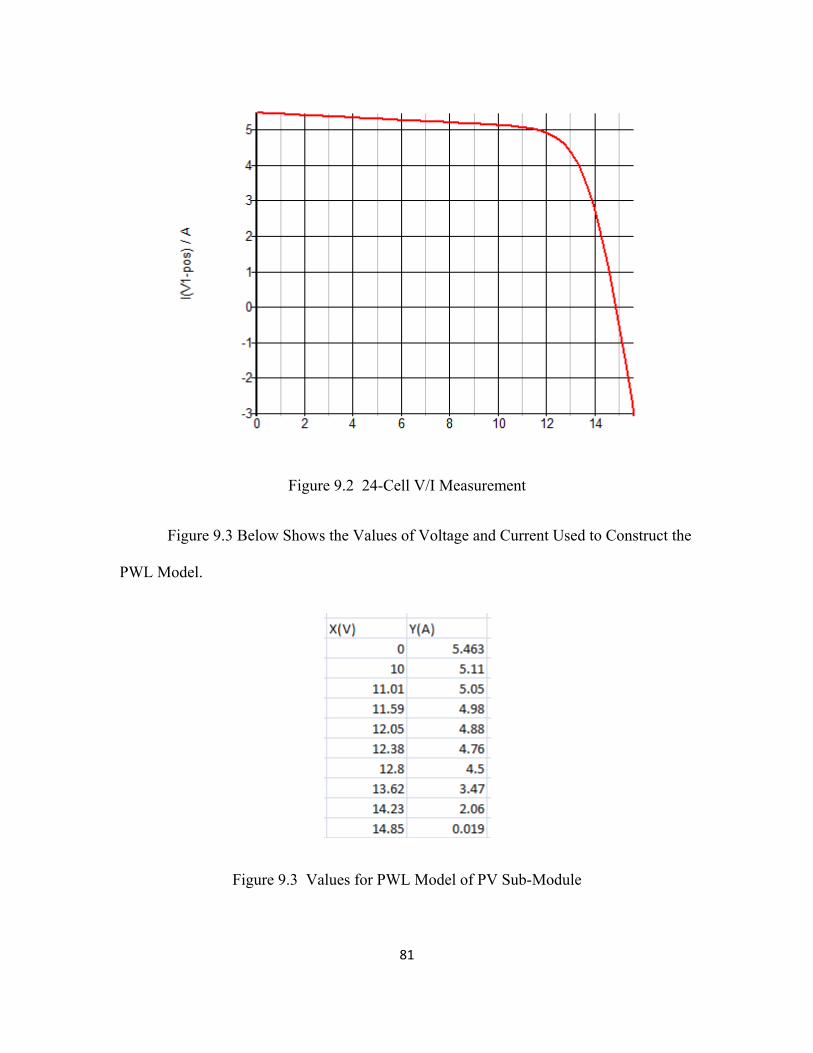
81
Figure 9.2 24-Cell V/I Measurement
Figure 9.3 Below Shows the Values of Voltage and Current Used to Construct the
PWL Model.
Figure 9.3 Values for PWL Model of PV Sub-Module
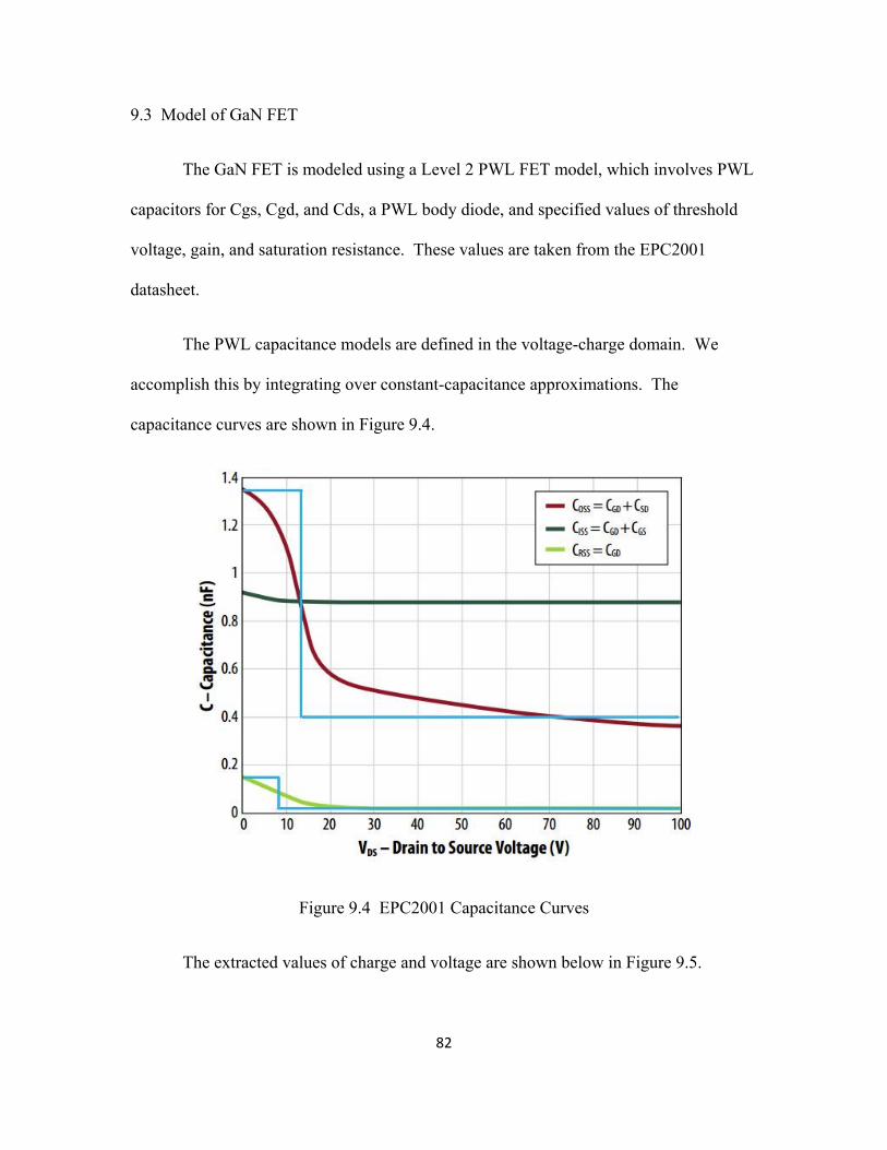
82
9.3 Model of GaN FET
The GaN FET is modeled using a Level 2 PWL FET model, which involves PWL
capacitors for Cgs, Cgd, and Cds, a PWL body diode, and specified values of threshold
voltage, gain, and saturation resistance. These values are taken from the EPC2001
datasheet.
The PWL capacitance models are defined in the voltage-charge domain. We
accomplish this by integrating over constant-capacitance approximations. The
capacitance curves are shown in Figure 9.4.
Figure 9.4 EPC2001 Capacitance Curves
The extracted values of charge and voltage are shown below in Figure 9.5.
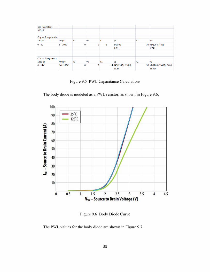
83
Figure 9.5 PWL Capacitance Calculations
The body diode is modeled as a PWL resistor, as shown in Figure 9.6.
Figure 9.6 Body Diode Curve
The PWL values for the body diode are shown in Figure 9.7.
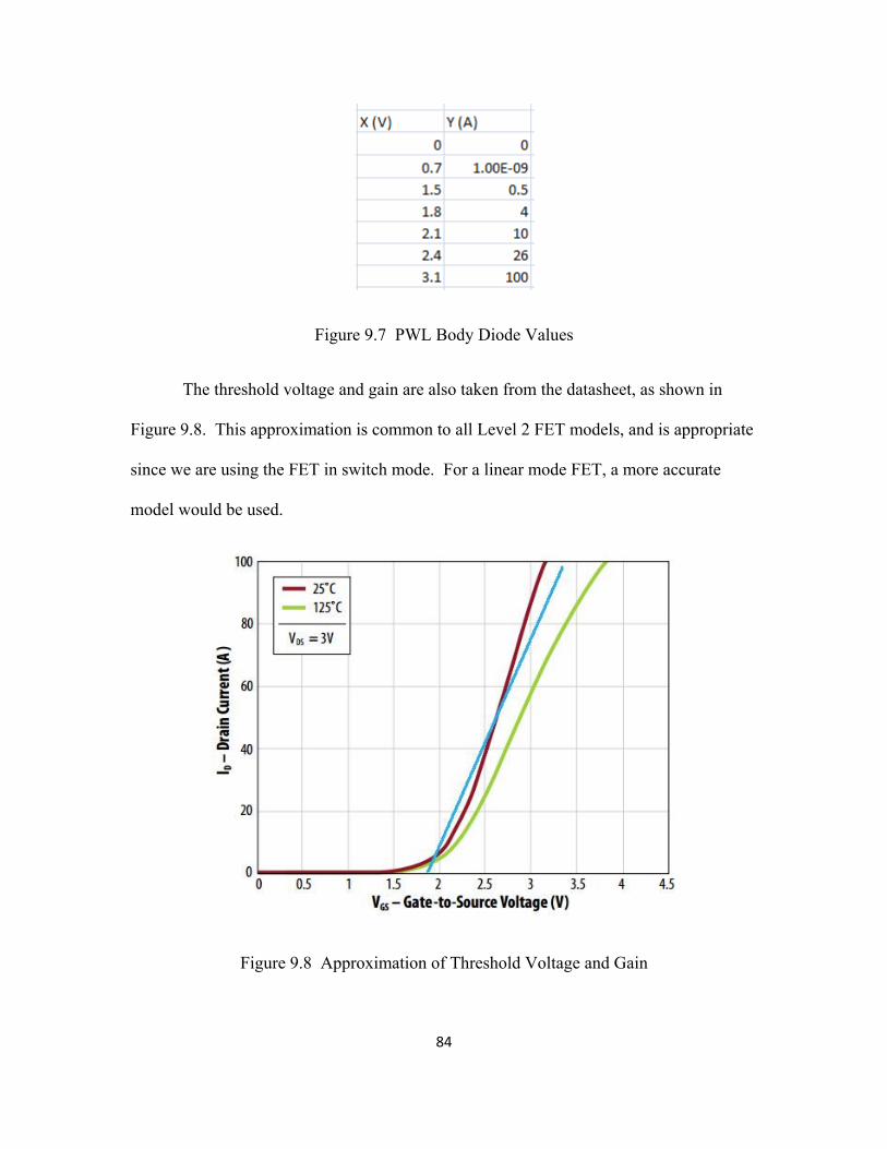
84
Figure 9.7 PWL Body Diode Values
The threshold voltage and gain are also taken from the datasheet, as shown in
Figure 9.8. This approximation is common to all Level 2 FET models, and is appropriate
since we are using the FET in switch mode. For a linear mode FET, a more accurate
model would be used.
Figure 9.8 Approximation of Threshold Voltage and Gain
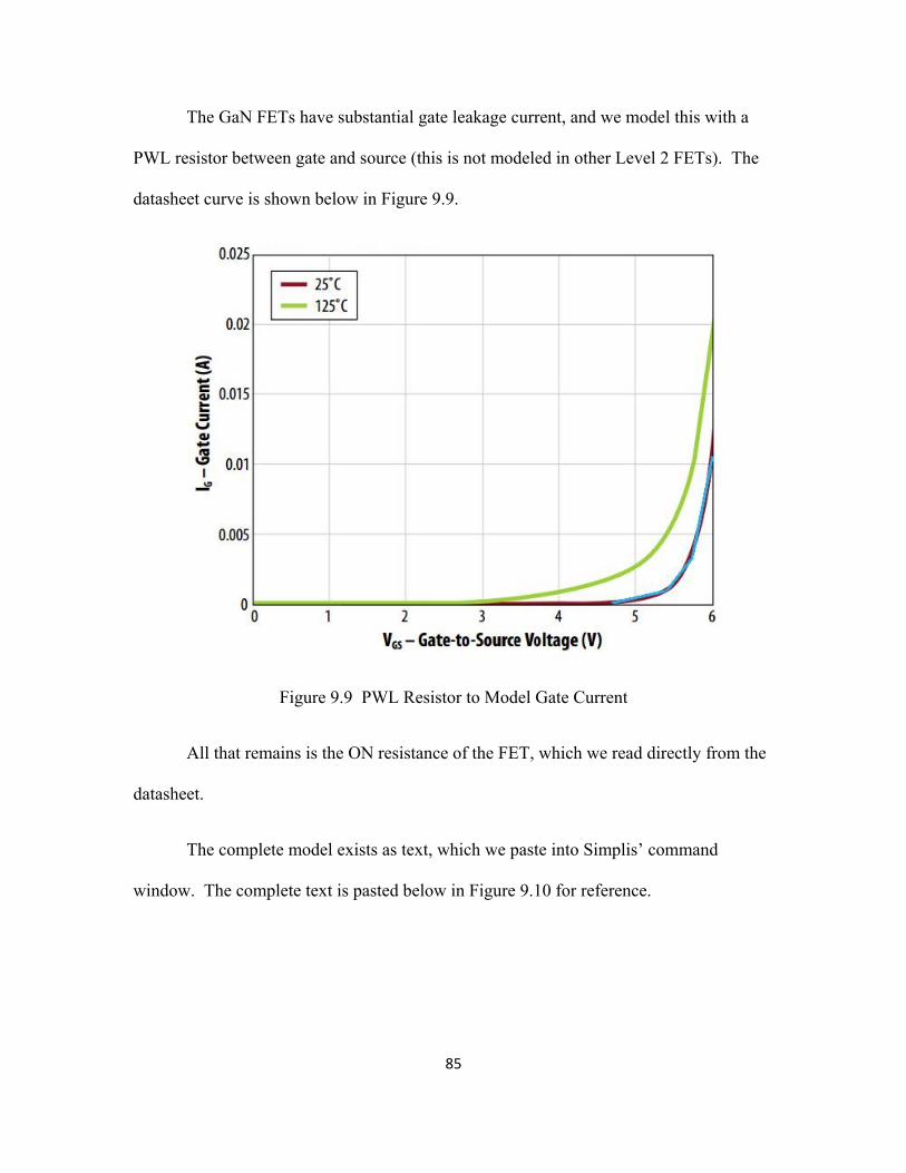
85
The GaN FETs have substantial gate leakage current, and we model this with a
PWL resistor between gate and source (this is not modeled in other Level 2 FETs). The
datasheet curve is shown below in Figure 9.9.
Figure 9.9 PWL Resistor to Model Gate Current
All that remains is the ON resistance of the FET, which we read directly from the
datasheet.
The complete model exists as text, which we paste into Simplis’ command
window. The complete text is pasted below in Figure 9.10 for reference.
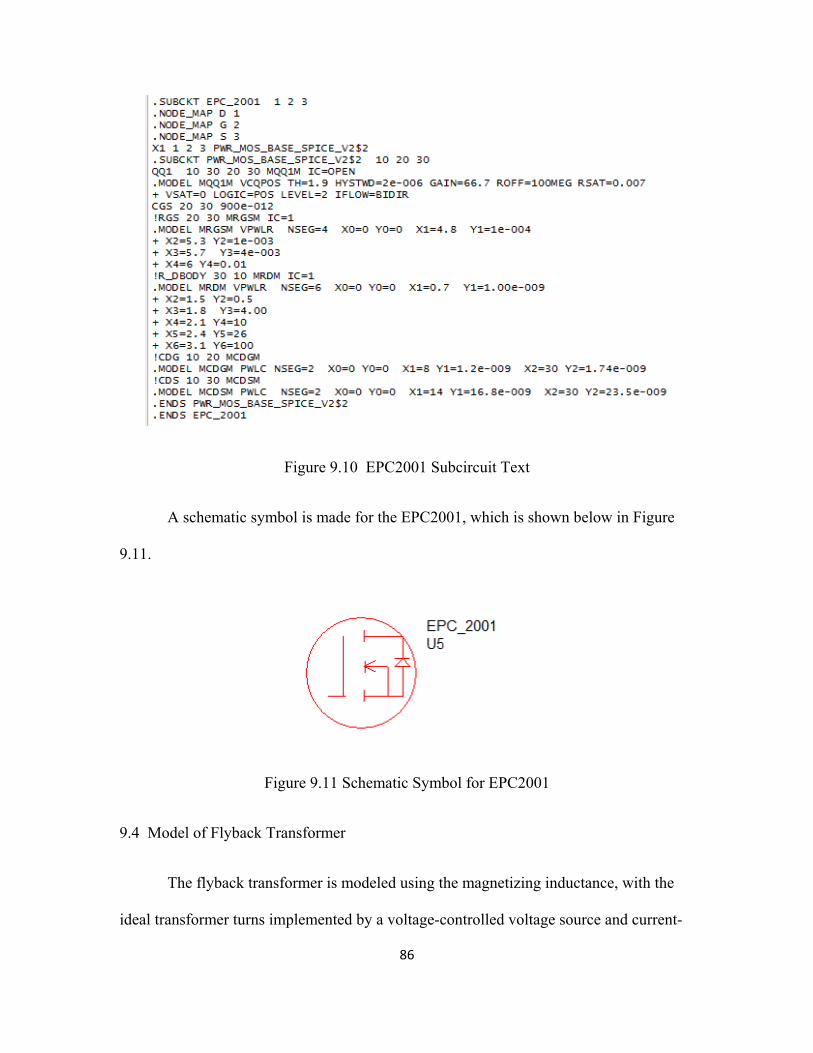
86
Figure 9.10 EPC2001 Subcircuit Text
A schematic symbol is made for the EPC2001, which is shown below in Figure
9.11.
Figure 9.11 Schematic Symbol for EPC2001
9.4 Model of Flyback Transformer
The flyback transformer is modeled using the magnetizing inductance, with the
ideal transformer turns implemented by a voltage-controlled voltage source and current-
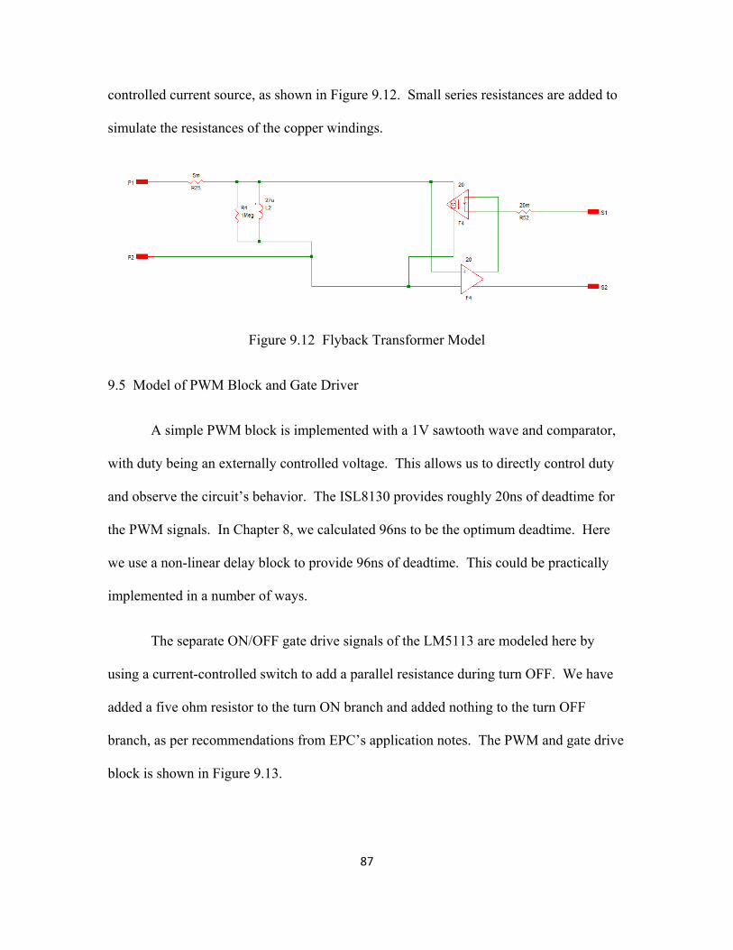
87
controlled current source, as shown in Figure 9.12. Small series resistances are added to
simulate the resistances of the copper windings.
Figure 9.12 Flyback Transformer Model
9.5 Model of PWM Block and Gate Driver
A simple PWM block is implemented with a 1V sawtooth wave and comparator,
with duty being an externally controlled voltage. This allows us to directly control duty
and observe the circuit’s behavior. The ISL8130 provides roughly 20ns of deadtime for
the PWM signals. In Chapter 8, we calculated 96ns to be the optimum deadtime. Here
we use a non-linear delay block to provide 96ns of deadtime. This could be practically
implemented in a number of ways.
The separate ON/OFF gate drive signals of the LM5113 are modeled here by
using a current-controlled switch to add a parallel resistance during turn OFF. We have
added a five ohm resistor to the turn ON branch and added nothing to the turn OFF
branch, as per recommendations from EPC’s application notes. The PWM and gate drive
block is shown in Figure 9.13.
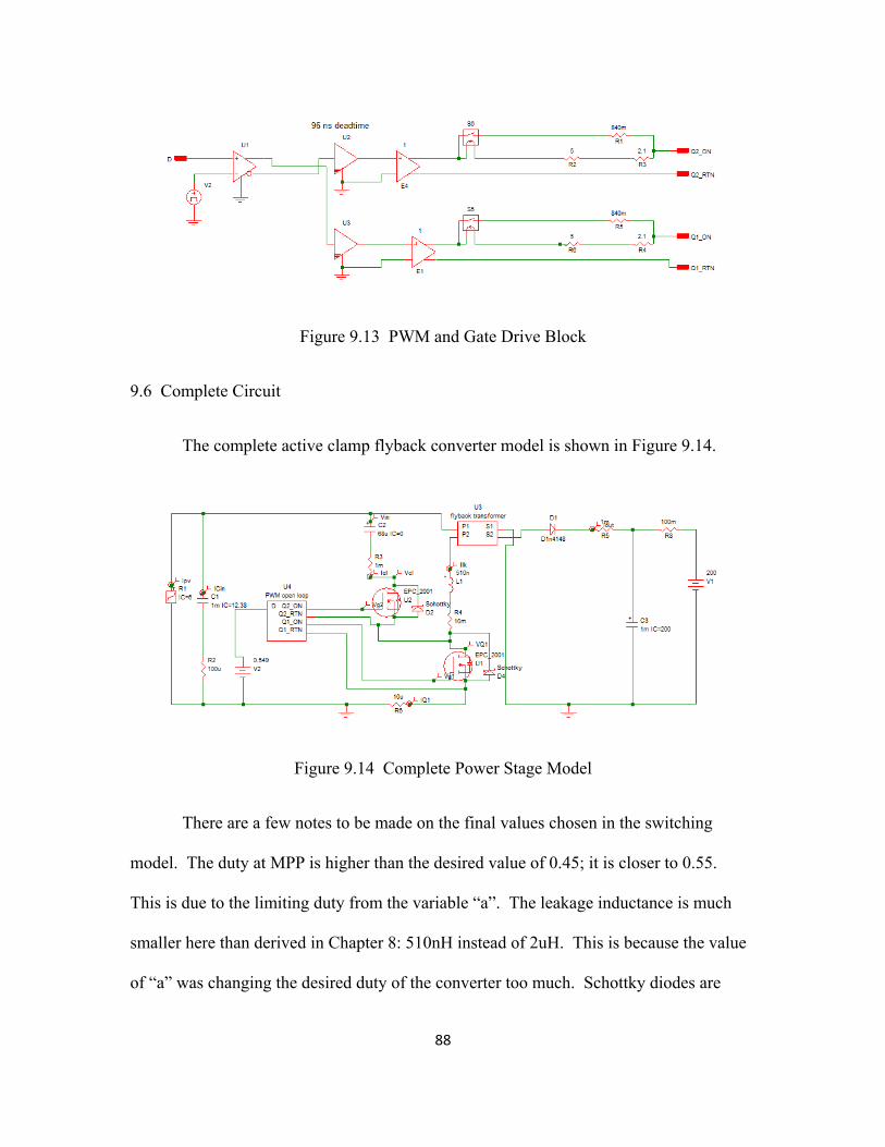
88
Figure 9.13 PWM and Gate Drive Block
9.6 Complete Circuit
The complete active clamp flyback converter model is shown in Figure 9.14.
Figure 9.14 Complete Power Stage Model
There are a few notes to be made on the final values chosen in the switching
model. The duty at MPP is higher than the desired value of 0.45; it is closer to 0.55.
This is due to the limiting duty from the variable “a”. The leakage inductance is much
smaller here than derived in Chapter 8: 510nH instead of 2uH. This is because the value
of “a” was changing the desired duty of the converter too much. Schottky diodes are
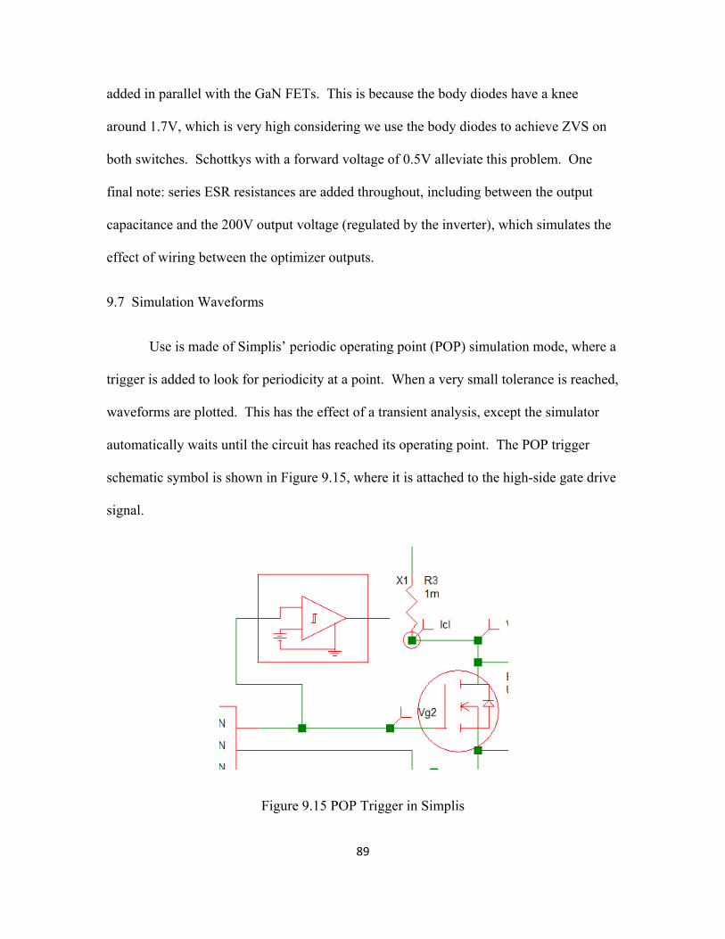
89
added in parallel with the GaN FETs. This is because the body diodes have a knee
around 1.7V, which is very high considering we use the body diodes to achieve ZVS on
both switches. Schottkys with a forward voltage of 0.5V alleviate this problem. One
final note: series ESR resistances are added throughout, including between the output
capacitance and the 200V output voltage (regulated by the inverter), which simulates the
effect of wiring between the optimizer outputs.
9.7 Simulation Waveforms
Use is made of Simplis’ periodic operating point (POP) simulation mode, where a
trigger is added to look for periodicity at a point. When a very small tolerance is reached,
waveforms are plotted. This has the effect of a transient analysis, except the simulator
automatically waits until the circuit has reached its operating point. The POP trigger
schematic symbol is shown in Figure 9.15, where it is attached to the high-side gate drive
signal.
Figure 9.15 POP Trigger in Simplis
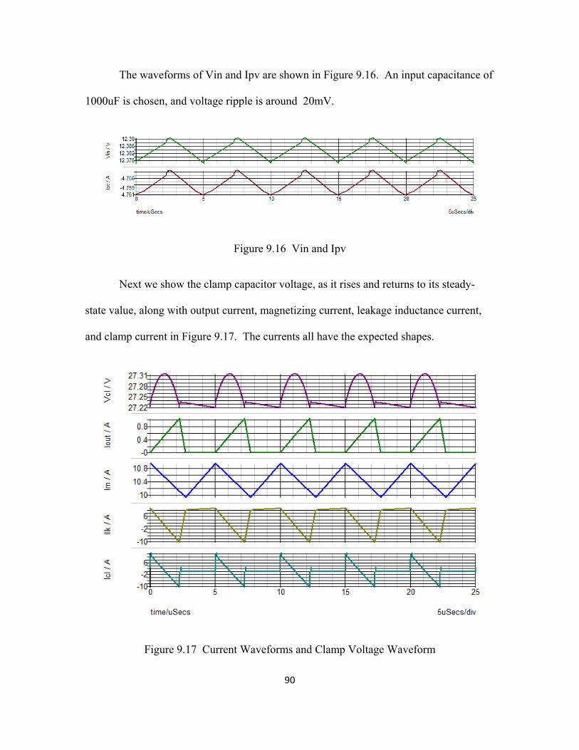
90
The waveforms of Vin and Ipv are shown in Figure 9.16. An input capacitance of
1000uF is chosen, and voltage ripple is around 20mV.
Figure 9.16 Vin and Ipv
Next we show the clamp capacitor voltage, as it rises and returns to its steady-
state value, along with output current, magnetizing current, leakage inductance current,
and clamp current in Figure 9.17. The currents all have the expected shapes.
Figure 9.17 Current Waveforms and Clamp Voltage Waveform
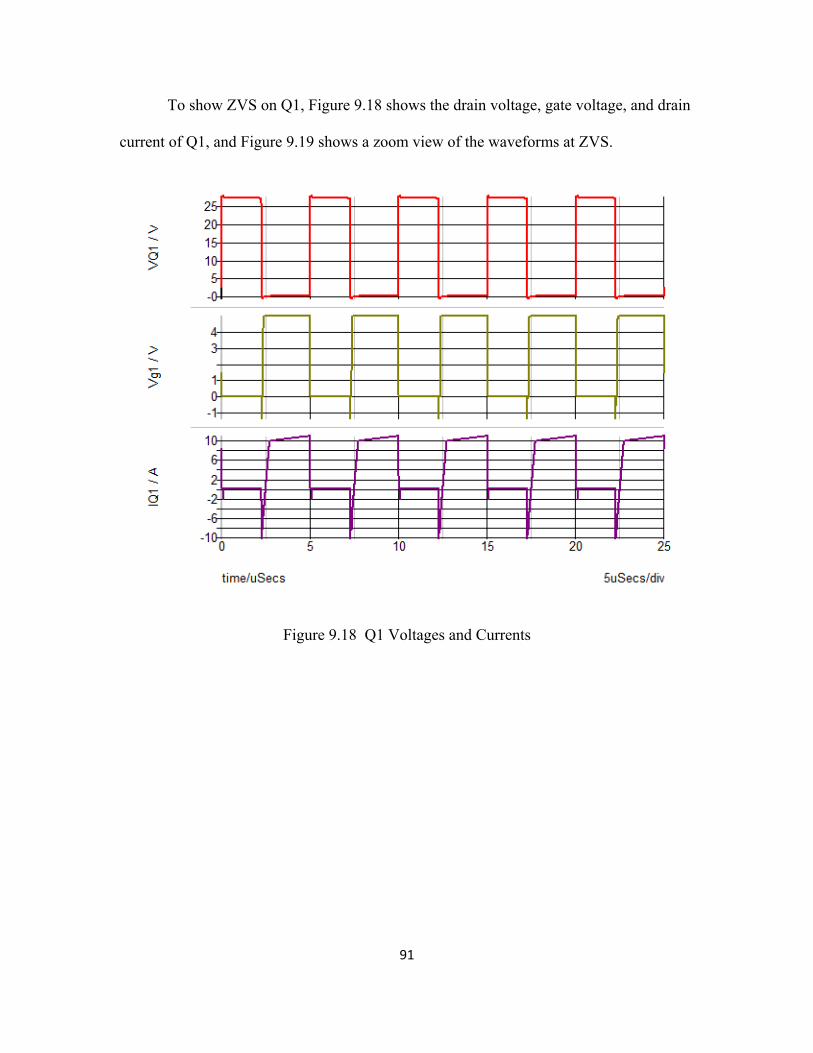
91
To show ZVS on Q1, Figure 9.18 shows the drain voltage, gate voltage, and drain
current of Q1, and Figure 9.19 shows a zoom view of the waveforms at ZVS.
Figure 9.18 Q1 Voltages and Currents
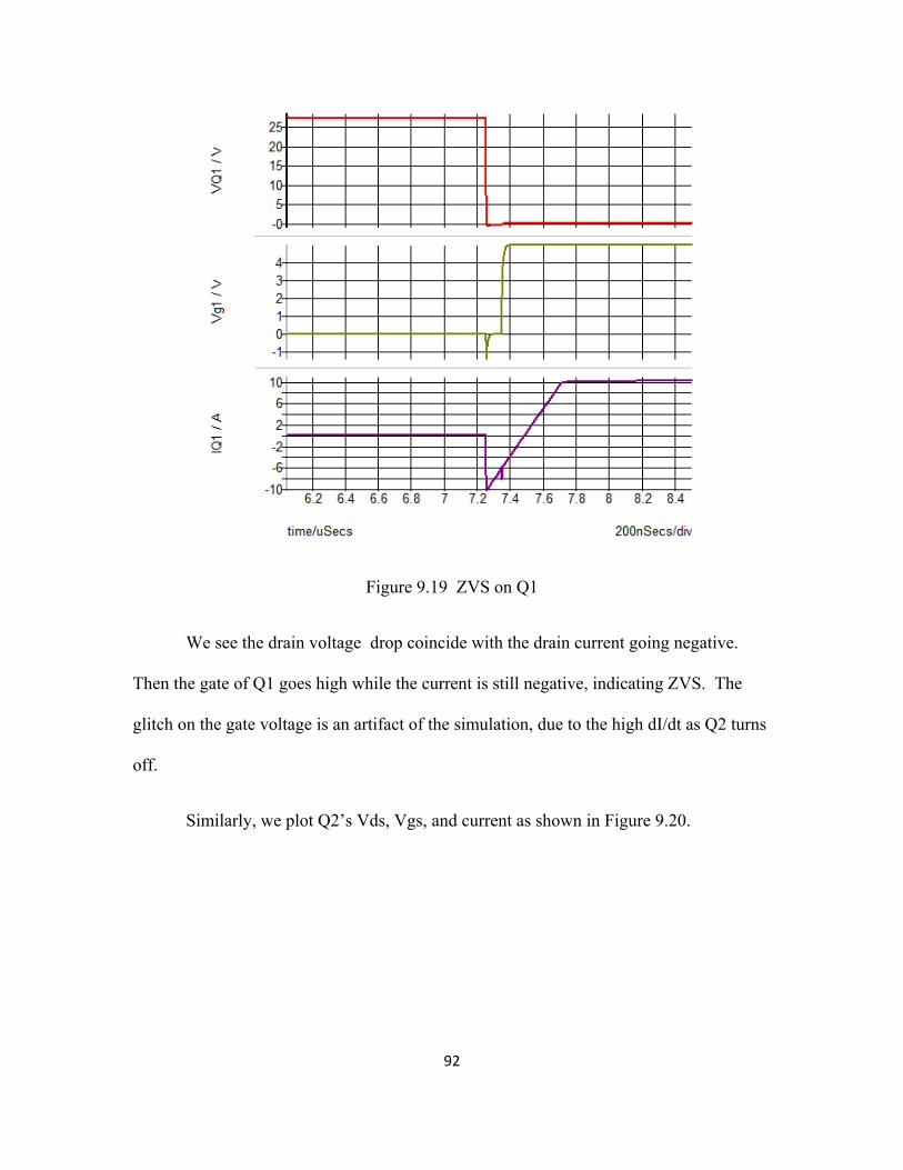
92
Figure 9.19 ZVS on Q1
We see the drain voltage drop coincide with the drain current going negative.
Then the gate of Q1 goes high while the current is still negative, indicating ZVS. The
glitch on the gate voltage is an artifact of the simulation, due to the high dI/dt as Q2 turns
off.
Similarly, we plot Q2’s Vds, Vgs, and current as shown in Figure 9.20.
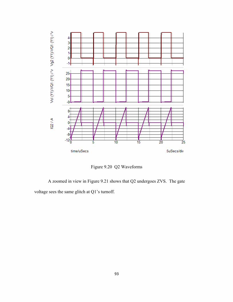
93
Figure 9.20 Q2 Waveforms
A zoomed in view in Figure 9.21 shows that Q2 undergoes ZVS. The gate
voltage sees the same glitch at Q1’s turnoff.
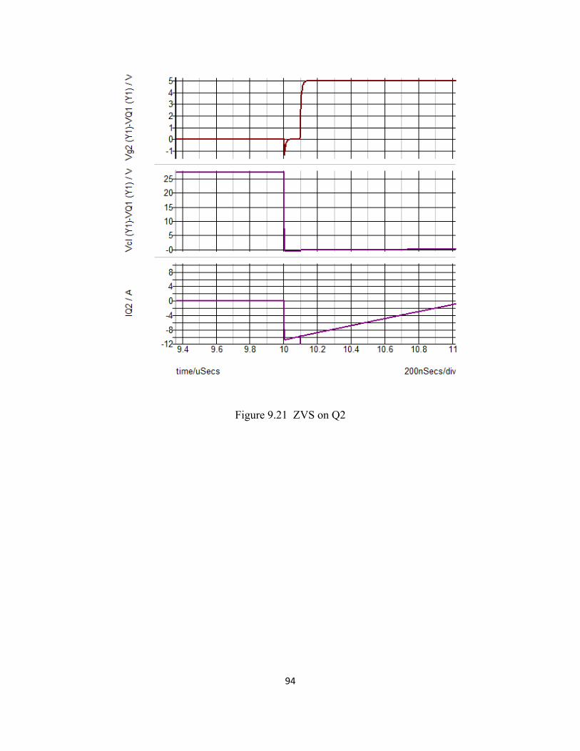
94
Figure 9.21 ZVS on Q2
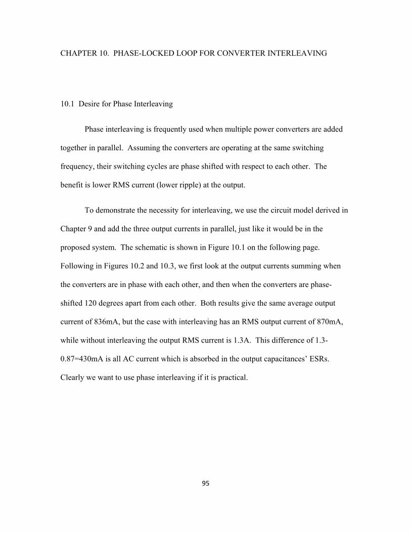
95
CHAPTER 10. PHASE-LOCKED LOOP FOR CONVERTER INTERLEAVING
10.1 Desire for Phase Interleaving
Phase interleaving is frequently used when multiple power converters are added
together in parallel. Assuming the converters are operating at the same switching
frequency, their switching cycles are phase shifted with respect to each other. The
benefit is lower RMS current (lower ripple) at the output.
To demonstrate the necessity for interleaving, we use the circuit model derived in
Chapter 9 and add the three output currents in parallel, just like it would be in the
proposed system. The schematic is shown in Figure 10.1 on the following page.
Following in Figures 10.2 and 10.3, we first look at the output currents summing when
the converters are in phase with each other, and then when the converters are phase-
shifted 120 degrees apart from each other. Both results give the same average output
current of 836mA, but the case with interleaving has an RMS output current of 870mA,
while without interleaving the output RMS current is 1.3A. This difference of 1.3-
0.87=430mA is all AC current which is absorbed in the output capacitances’ ESRs.
Clearly we want to use phase interleaving if it is practical.
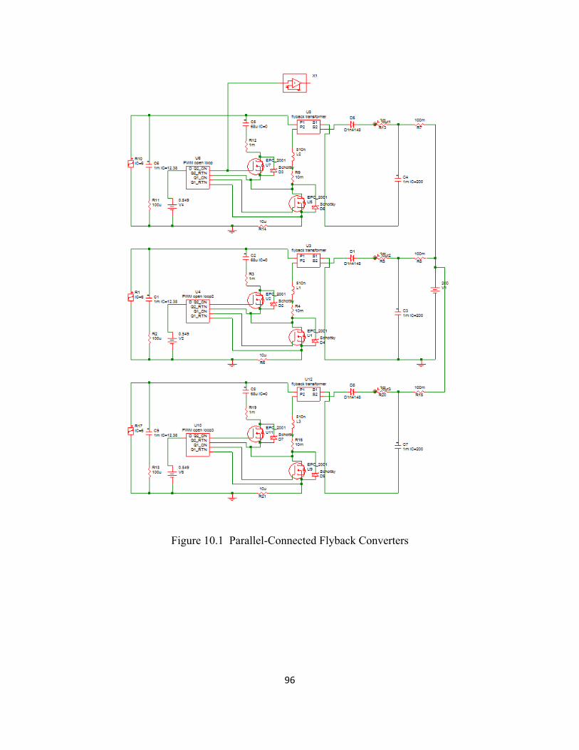
96
Figure 10.1 Parallel-Connected Flyback Converters
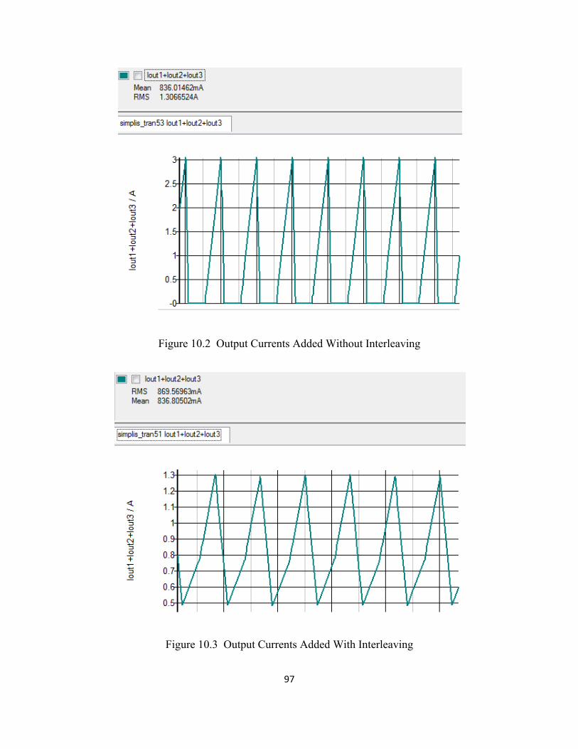
97
Figure 10.2 Output Currents Added Without Interleaving
Figure 10.3 Output Currents Added With Interleaving
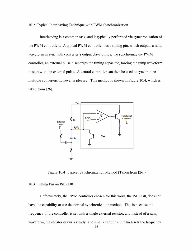
98
10.2 Typical Interleaving Technique with PWM Synchronization
Interleaving is a common task, and is typically performed via synchronization of
the PWM controllers. A typical PWM controller has a timing pin, which outputs a ramp
waveform in sync with converter’s output drive pulses. To synchronize the PWM
controller, an external pulse discharges the timing capacitor, forcing the ramp waveform
to start with the external pulse. A central controller can then be used to synchronize
multiple converters however is pleased. This method is shown in Figure 10.4, which is
taken from [26].
Figure 10.4 Typical Synchronization Method (Taken from [26])
10.3 Timing Pin on ISL8130
Unfortunately, the PWM controller chosen for this work, the ISL8130, does not
have the capability to use the normal synchronization method. This is because the
frequency of the controller is set with a single external resistor, and instead of a ramp
waveform, the resistor draws a steady (and small) DC current, which sets the frequency
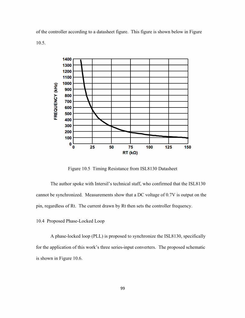
99
of the controller according to a datasheet figure. This figure is shown below in Figure
10.5.
Figure 10.5 Timing Resistance from ISL8130 Datasheet
The author spoke with Intersil’s technical staff, who confirmed that the ISL8130
cannot be synchronized. Measurements show that a DC voltage of 0.7V is output on the
pin, regardless of Rt. The current drawn by Rt then sets the controller frequency.
10.4 Proposed Phase-Locked Loop
A phase-locked loop (PLL) is proposed to synchronize the ISL8130, specifically
for the application of this work’s three series-input converters. The proposed schematic
is shown in Figure 10.6.
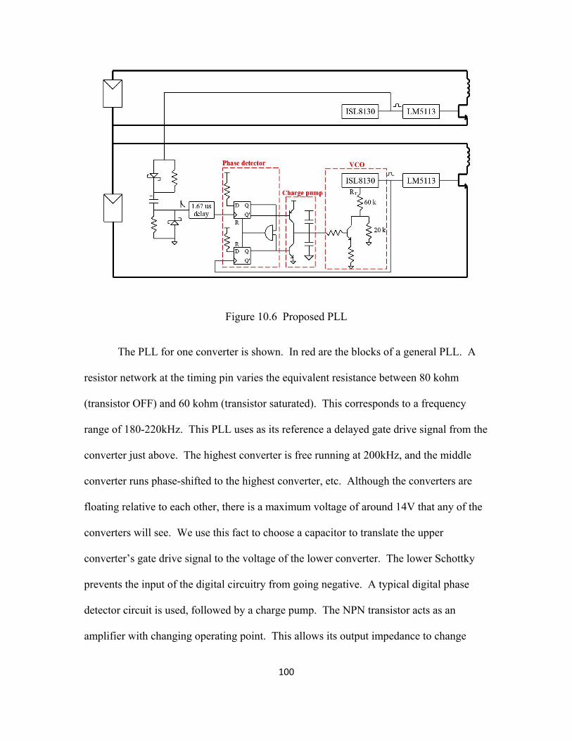
100
Figure 10.6 Proposed PLL
The PLL for one converter is shown. In red are the blocks of a general PLL. A
resistor network at the timing pin varies the equivalent resistance between 80 kohm
(transistor OFF) and 60 kohm (transistor saturated). This corresponds to a frequency
range of 180-220kHz. This PLL uses as its reference a delayed gate drive signal from the
converter just above. The highest converter is free running at 200kHz, and the middle
converter runs phase-shifted to the highest converter, etc. Although the converters are
floating relative to each other, there is a maximum voltage of around 14V that any of the
converters will see. We use this fact to choose a capacitor to translate the upper
converter’s gate drive signal to the voltage of the lower converter. The lower Schottky
prevents the input of the digital circuitry from going negative. A typical digital phase
detector circuit is used, followed by a charge pump. The NPN transistor acts as an
amplifier with changing operating point. This allows its output impedance to change
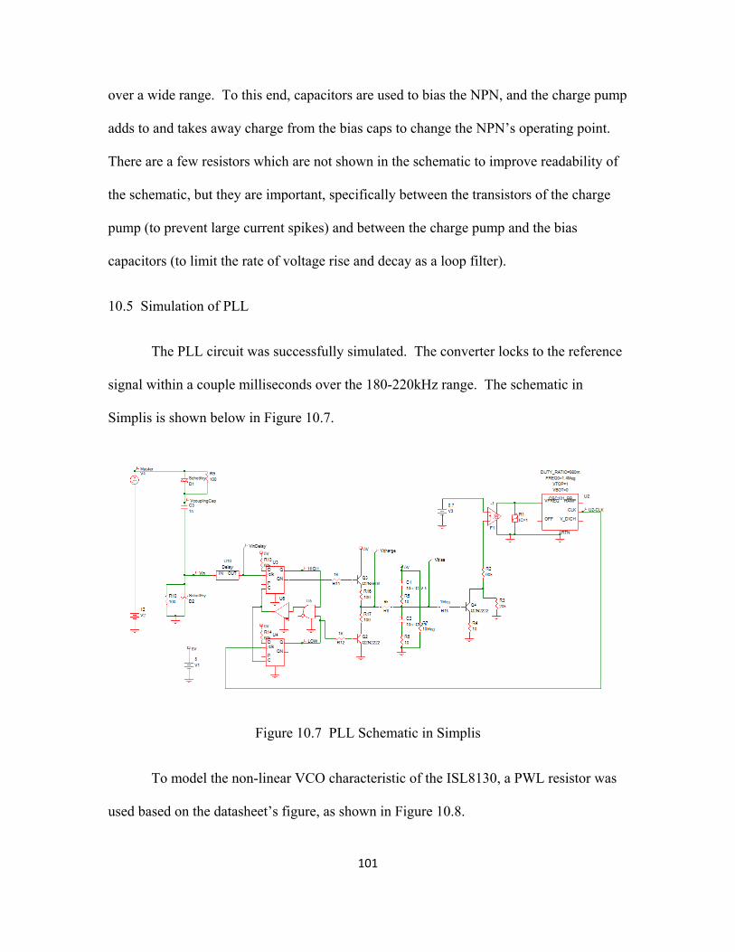
101
over a wide range. To this end, capacitors are used to bias the NPN, and the charge pump
adds to and takes away charge from the bias caps to change the NPN’s operating point.
There are a few resistors which are not shown in the schematic to improve readability of
the schematic, but they are important, specifically between the transistors of the charge
pump (to prevent large current spikes) and between the charge pump and the bias
capacitors (to limit the rate of voltage rise and decay as a loop filter).
10.5 Simulation of PLL
The PLL circuit was successfully simulated. The converter locks to the reference
signal within a couple milliseconds over the 180-220kHz range. The schematic in
Simplis is shown below in Figure 10.7.
Figure 10.7 PLL Schematic in Simplis
To model the non-linear VCO characteristic of the ISL8130, a PWL resistor was
used based on the datasheet’s figure, as shown in Figure 10.8.
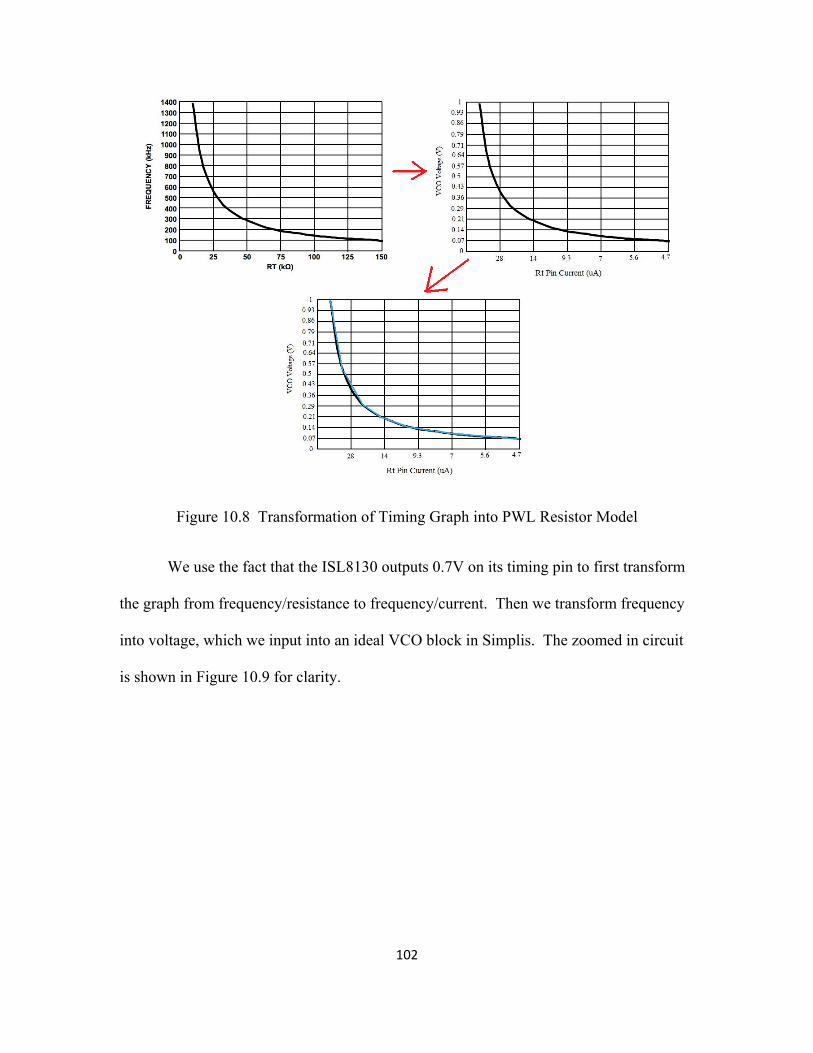
102
Figure 10.8 Transformation of Timing Graph into PWL Resistor Model
We use the fact that the ISL8130 outputs 0.7V on its timing pin to first transform
the graph from frequency/resistance to frequency/current. Then we transform frequency
into voltage, which we input into an ideal VCO block in Simplis. The zoomed in circuit
is shown in Figure 10.9 for clarity.
103
Figure 10.9 Zoomed in Schematic of Equivalent Non-Linear VCO
Since no digital delay blocks were readily available in the Simplis library, a delay
block was made using a timer and a 100MHz clock, as shown in Figure 10.10.
Figure 10.10 Delay Block in Simplis
The waveforms at steady-state are shown in Figure 10.11.
104
Figure 10.11 PLL During Lock
One by one, let us describe the waveforms from the top down. First we have the
pulse at the digital circuit input, which reaches 5V for a few tens of ns and briefly goes
negative, as far as the Schottky forward voltage of around -0.3V. Next we see the level-
shift capacitor voltage, which shifts a 0-5V signal to a 12-17V signal, with rounding of
the edges being a good sign that the input pulse to the phase detector has ample width.

105
Next we have the voltage at the output of the charge pump. The brief pulses happen
while the charge pump transistors are simultaneously conducting. This overlap period is
on purpose and comes from a small delay block between the AND gate and the reset of
the flip-flops. This prevents low-frequency oscillations modulating the PLL waveforms.
Next we have the NPN bias voltage, which is at 0.6V, in its active region. Next we see
the converter’s output pulses above the high converter’s pulses. They are phase shifted
by 120 degrees, confirming operation of the circuit. The LOW and HIGH signals share a
brief overlap period as mentioned. The last waveform is the delayed input pulse, which is
perfectly locked to the output pulse.
106
CHAPTER 11. DISCUSSION AND CONCLUSIONS
We have detailed the design of an active clamp flyback converter using GaN
FETs, for use in a sub-module DC converter performing MPPT. All efforts were made to
maximize efficiency, to justify the additional cost of using module-level power
electronics. The design in this work uses an autonomous control scheme, where the
converters turn on and off naturally with the sunrise and sunset. This system can operate
as an add-on for existing panels. Many manufacturers of PV modules are currently
installing DC optimizers into their modules’ junction boxes, and the design in this work
would be a good candidate, especially if system cost is valued over system control and
monitoring, as this design uses autonomous control with the intent of avoiding external
communication. Furthermore, the design consists of three equal converters; many more
small converters can be manufactured to reduce the cost per unit. Although no external
control is needed to operate, the system designer may desire to have an external reset
signal come from the system inverter to the DC optimizers, for safety purposes. This can
easily be added as an I/O input to the microcontroller.
Extensive analysis has been performed on the active clamp flyback stage, to
ensure stable operation over all operating points. This is particularly important for the
converter in this report, as operating points can vary widely over temperature and
sunlight. We have derived a handful of design constraints. These constraints can be used
as a balance to choose at which low current levels ZVS will be achieved, and to reduce
converter noise. The low-side clamp was found to be advantageous over the high-side

107
clamp, due to a smaller clamp voltage and due to lower RMS currents on the input of the
converter (where currents are highest). We have used an algorithm to demonstrate the
stability of clamp capacitor voltages, which are stable for off times less than one half the
resonant period.
We have modeled the EPC2001, a GaN FET, as a PWL model in Simplis,
including the body diode and gate leakage, and demonstrated its operation with
simulations. We used GaN FETs in the active clamp flyback converter, for both the
primary switching FET and the active clamp FET. The existence of a gate drive IC
tailored for eGaN (the LM5113) made the gate drive design very simple.
The PLL designed in this work is unique, insofar as it is used to
synchronize PWM controllers for PV sub-module series-connected converters. The
tolerable voltage difference of 12-14V between converters proved to be useful in
decoupling the gate drive signals between the converters. This is a classical PLL, with
the main difference being that the non-linear characteristic of the timing resistor versus
frequency leads to the VCO in the PLL having a non-linear characteristic. Nonetheless,
we are biasing frequencies in a small band, such that the characteristic approaches that of
a linear VCO.
Future work includes the implementation of this converter onto a PV module, for
extensive testing over weather conditions. For testing it may be necessary to add
additional data logging circuitry. After extensive data is taken, the design can further be
tuned for efficiency, and for cost.
108
REFERENCES
[1] “Residential Renewable Energy Tax Credit”, from dsireusa.org. [2] “Renewables 2014 Global Status Report”, from ren21.net. [3] “Renewables Portfolio Standard”, from dsireusa.org. [4] “Solar Industry Data”, from seia.org. [5] “Solar Module OEMs Seeking Advantage with Inverter Electronics”, from greentechmedia.com. [6] “Products”, from tigoenergy.com. [7] P. Grana. “The Microinverter and DC Optimizer Landscape 2014: The Evolution From Market Niche to Market Success”, GTM Research, January 2014. [8] “Solar Cell Operation”, from pveducation.org/pvcdrom. [9] W. Shockley and H. Quiesser. “Detailed Balance Limit of Efficiency of p-n Junction Solar Cells”, Journal of Applied Physics, Vol. 32, Issue 3. [10] T. Tiedje, E. Yablonovitch, G. Cody, and B. Brooks. “Limiting Efficiency of Silicon Solar Cells”, IEEE Transactions on Electron Devices, Vol. ED-31, No. 5. [11] R. King, R. Sinton, and R. Swanson. “Studies of Diffused Phosphorus Emitters: Saturation Current, Surface Recombination Velocity, and Quantum Efficiency”, IEEE Transactions on Electron Devices, Vol. 37, No. 2. [12] R. Pierret. “Semiconductor Device Fundamentals”, Pearson Education Inc., 2006 [13] T.J. McMahon, T.S. Basso, and S.R. Rummel. “Cell Shunt Resistance and Photovoltaic Module Performance”, Conference Record of the Twenty Fifth IEEE Photovoltaic Specialists Conference, 1996. [14] H.K. Gummel and H.C. Poon. “An Integral Charge Control Model of Bipolar Transistors”, The Bell System Technical Journal, Vol. 49, Issue 5.

109
[15] Y. Wang, P. Zhang, W. Li, and N.H. Kanan. “Comparative Analysis of the Reliability of Grid-Connected Photovoltaic Power Systems”, 2012 IEEE Power and Energy Society General Meeting. [16] S. Bifaretti, V. Iacovone, L. Cina, and E. Buffone. “Global MPPT Method for Partially Shaded Photovoltaic Modules”, 2012 IEEE Energy Conversion Congress and Exposition. [17] H. Patel, and V. Agarwal. “Maximum Power Point Tracking Scheme for PV Systems Operating Under Partially Shaded Conditions”, IEEE Transactions on Industrial Electronics, Vol. 55, Issue 4. [18] E. Koutroulis, and F. Blaabjerg. “A New Technique for Tracking the Global Maximum Power Point of PV Arrays Operating Under Partial-Shading Conditions”, IEEE Journal of Photovoltaics, Vol. 2, Issue 2. [19] “Power extractor for impedance matching”, Tigo Energy, US patent #20080122449. [20] J. Stauth, M. Seeman, and K. Kesarwani. “Resonant Switched-Capacitor Converters for Sub-module Distributed Photovoltaic Power Management”, IEEE Transactions on Power Electronics, Vol. 28, No. 3. [21] R. Pilawa-Podgurski and D. Perreault. “Submodule Integrated Distributed Maximum Power Point Tracking for Solar Photovoltaic Applications”, IEEE Transactions on Power Electronics, Vol. 28, No. 6. [22] AN-4147: “Design Guidelines for RCD Snubber of Flyback Converters”, Fairchild Semiconductor. [23] R. Watson, F. Lee, and G Hua. “Utilization of an Active-Clamp Circuit to Achieve Soft Switching in Flyback Converters”, IEEE Transactions on Power Electronics, Vol. 11, No. 1. [24] M. Chen and J. Sun. “A General Approach to Average Modeling and Analysis of Active-Clamped Converters”, Twentieth Annual IEEE Appled Power Electronics Conference and Exposition, 2005.

110
[25] A. Lidow and M. de Rooij. “eGaN FET Electrical Characteristics”, From epc-co.com. [26] Fairchild Semiconductor. “Application Note 42034: Synchronizing the ML4824 to Wide Frequency Ranges”.
Related Documents


