www.infineon.com Please note that Cypress is an Infineon Technologies Company. The document following this cover page is marked as “Cypress” document as this is the company that originally developed the product. Please note that Infineon will continue to offer the product to new and existing customers as part of the Infineon product portfolio. Continuity of document content The fact that Infineon offers the following product as part of the Infineon product portfolio does not lead to any changes to this document. Future revisions will occur when appropriate, and any changes will be set out on the document history page. Continuity of ordering part numbers Infineon continues to support existing part numbers. Please continue to use the ordering part numbers listed in the datasheet for ordering.

Welcome message from author
This document is posted to help you gain knowledge. Please leave a comment to let me know what you think about it! Share it to your friends and learn new things together.
Transcript
www.infineon.com
Please note that Cypress is an Infineon Technologies Company.The document following this cover page is marked as “Cypress” document as this is the company that originally developed the product. Please note that Infineon will continue to offer the product to new and existing customers as part of the Infineon product portfolio.
Continuity of document contentThe fact that Infineon offers the following product as part of the Infineon product portfolio does not lead to any changes to this document. Future revisions will occur when appropriate, and any changes will be set out on the document history page.
Continuity of ordering part numbersInfineon continues to support existing part numbers. Please continue to use the ordering part numbers listed in the datasheet for ordering.
PRELIMINARY CYW43340
Single-Chip, Dual-Band (2.4 GHz/5 GHz)IEEE 802.11 a/b/g/n MAC/Baseband/
Radio with Integrated Bluetooth 5.0
Cypress Semiconductor Corporation • 198 Champion Court • San Jose, CA 95134-1709 • 408-943-2600Document Number: 002-14943 Rev. *N Revised Wednesday, March 24, 2021
General Description
The Cypress CYW43340 single–chip quad–radio device provides the highest level of integration for wearables, Internet of Things andgateway applications, with integrated dual band (2.4 GHz / 5 GHz) IEEE 802.11 a/b/g and single–stream IEEE 802.11n MAC/baseband/radio, and Bluetooth 5.0. The CYW43340 includes integrated power amplifiers and LNAs for the 2.4 GHz and 5 GHz WLANbands, and an integrated 2.4 GHz T/R switch. This greatly reduces the external part count, PCB footprint, and cost of the solution.
Using advanced design techniques and process technology to reduce active and idle power, the CYW43340 is designed to addressthe needs of mobile devices that require minimal power consumption and compact size. It includes a power management unit whichsimplifies the system power topology and allows for operation directly from a mobile platform battery while maximizing battery life.
The CYW43340 implements the highly sophisticated Enhanced Collaborative Coexistence algorithms and hardware mechanisms,allowing for an extremely collaborative Bluetooth coexistence scheme along with coexistence support for external radios (such ascellular and LTE, GPS, WiMAX, and Ultra–Wideband) and a single shared 2.4 GHz antenna for Bluetooth and WLAN. As a result,enhanced overall quality for simultaneous voice, video, and data transmission in an IoT or wearable application is achieved.
For the WLAN section, two host interface options are included: an SDIO v2.0 interface and a High-Speed Inter-Chip (HSIC) interface(a USB 2.0 derivative for short-distance on-board connections). An independent, high-speed UART is provided for the Bluetooth hostinterface.
Features
IEEE 802.11x Key Features
Dual–band 2.4 GHz and 5 GHz IEEE 802.11 a/b/g/n
Single–stream IEEE 802.11n support for 20 MHz and 40 MHz channels provides PHY layer rates up to 150 Mbps for typical upper–layer throughput in excess of 90 Mbps.
Supports a single 2.4 GHz antenna shared between WLAN and Bluetooth.
Shared Bluetooth and 2.4 GHz WLAN receive signal path elimi-nates the need for an external power splitter while maintaining excellent sensitivity for both Bluetooth and WLAN.
Internal fractional nPLL allows support for a wide range of reference clock frequencies
Supports IEEE 802.15.2 external coexistence interface to optimize bandwidth utilization with other co–located wireless technologies such as GPS, WiMAX, or UWB
Supports standard SDIO v2.0 host interfaces.
Alternative host interface supports HSIC v1.0 (short–distance USB device)
Integrated ARM® Cortex–M3™ processor and on–chip memory for complete WLAN subsystem functionality, minimizing the need to wake up the applications processor for standard WLAN functions. This allows for further minimization of power consumption, while maintaining the ability to field upgrade with future features. On–chip memory includes 512 KB SRAM and 640 KB ROM.
OneDriver™ software architecture for easy migration from existing embedded WLAN and Bluetooth devices as well as future devices.
Bluetooth Key Features
Qualified for Bluetooth Core Specification 5.0: QDID: 108508 Declaration ID: D035926
Bluetooth Class 1 or Class 2 transmitter operation
Supports extended Synchronous Connections (eSCO), for enhanced voice quality by allowing for retransmission of dropped packets.
Adaptive Frequency Hopping (AFH) for reducing radio frequency interference
Interface support: Host Controller Interface (HCI) using a high-speed UART interface and PCM for audio data
Low power consumption improves battery life of handheld devices.
Supports multiple simultaneous Advanced Audio Distribution Profiles (A2DP) for stereo sound.
Automatic frequency detection for standard crystal and TCXO values
General Features
Supports battery voltage range from 2.9V to 4.8V supplies with internal switching regulator.
Programmable dynamic power management
3072-bit OTP for storing board parameters
Routable on low–cost 1x1 PCB stack–ups
141-ball WLBGA package(5.67 mm × 4.47 mm, 0.4 mm pitch)
Document Number: 002-14943 Rev. *N Page 2 of 96
PRELIMINARY CYW43340
Security: WPA™ and WPA2™ (Personal) support for powerful encryp-
tion and authentication AES in WLAN hardware for faster data encryption and IEEE
802.11i compatibility
Reference WLAN subsystem provides Cisco® Compatible Extensions (CCX, CCX 2.0, CCX 3.0, CCX 4.0, CCX 5.0)
Reference WLAN subsystem provides Wi–Fi Protected Set-up (WPS)
Worldwide regulatory support: Global products supported with worldwide homologated design
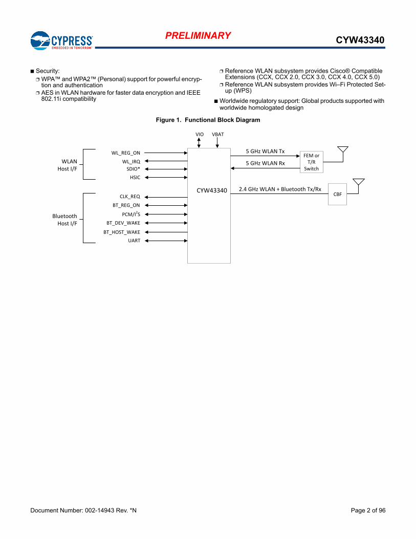
Figure 1. Functional Block Diagram
VIO VBAT
CYW43340
WLAN Host I/F
BluetoothHost I/F
WL_REG_ON
SDIO*
WL_IRQ
BT_REG_ON
UART
BT_DEV_WAKE
BT_HOST_WAKE
CLK_REQ
HSIC
PCM/I2S
2.4 GHz WLAN + Bluetooth Tx/RxCBF
FEM orT/R
Switch
5 GHz WLAN Tx
5 GHz WLAN Rx
Document Number: 002-14943 Rev. *N Page 3 of 96
PRELIMINARY CYW43340
Contents1. Introduction ................................................................... 4
1.1 Overview ............................................................... 41.2 Features ................................................................ 51.3 Standards Compliance .......................................... 6
2. Power Supplies and Power Management ................... 72.1 Power Supply Topology ........................................ 72.2 WLAN Power Management ................................... 92.3 PMU Sequencing .................................................. 92.4 Power-Off Shutdown ........................................... 102.5 Power-Up/Power-Down/Reset Circuits ............... 10
3. Frequency References ............................................... 113.1 Crystal Interface and Clock Generation .............. 113.2 TCXO .................................................................. 113.3 Frequency Selection ............................................ 133.4 External 32.768 kHz Low-Power Oscillator ......... 14
4. Bluetooth Subsystem Overview ................................ 154.1 Features .............................................................. 154.2 Bluetooth Radio ................................................... 16
5. Bluetooth Baseband Core ......................................... 175.1 Bluetooth 5.0 Features ........................................ 175.2 Link Control Layer ............................................... 175.3 Test Mode Support .............................................. 175.4 Bluetooth Power Management Unit ..................... 185.5 Adaptive Frequency Hopping .............................. 215.6 Advanced Bluetooth/WLAN Coexistence ............ 215.7 Fast Connection (Interlaced Page and Inquiry
Scans) ................................................................ 216. Microprocessor and Memory Unit for Bluetooth ..... 22
6.1 RAM, ROM, and Patch Memory .......................... 226.2 Reset ................................................................... 22
7. Bluetooth Peripheral Transport Unit ........................237.1 PCM Interface ..................................................... 237.2 UART Interface .................................................... 307.3 I2S Interface ........................................................ 31
8. WLAN Global Functions ............................................ 348.1 WLAN CPU and Memory Subsystem .................. 348.2 One-Time Programmable Memory ...................... 348.3 GPIO Interface .................................................... 348.4 External Coexistence Interface ........................... 348.5 UART Interface .................................................... 358.6 JTAG Interface .................................................... 35
9. WLAN Host Interfaces ................................................ 369.1 SDIO v2.0 ............................................................ 369.2 HSIC Interface ..................................................... 38
10. Wireless LAN MAC and PHY ................................... 3910.1 MAC Features ................................................... 3910.2 WLAN PHY Description .....................................42
11. WLAN Radio Subsystem .......................................... 4411.1 Receiver Path .................................................... 4411.2 Transmit Path .................................................... 4411.3 Calibration ......................................................... 44
12. Pinout and Signal Descriptions .............................. 45
12.1 Signal Assignments ........................................... 4512.2 Signal Descriptions ............................................ 4512.3 I/O States .......................................................... 54
13. DC Characteristics ................................................... 5713.1 Absolute Maximum Ratings ............................... 5713.2 Environmental Ratings ...................................... 5713.3 Electrostatic Discharge Specifications .............. 5813.4 Recommended Operating Conditions and DC
Characteristics .................................................... 5814. Bluetooth RF Specifications .................................... 6015. WLAN RF Specifications .......................................... 67
15.1 Introduction ........................................................ 6715.2 2.4 GHz Band General RF Specifications ......... 6815.3 WLAN 2.4 GHz Receiver Performance
Specifications ..................................................... 6815.4 WLAN 2.4 GHz Transmitter Performance
Specifications ..................................................... 7215.5 WLAN 5 GHz Receiver Performance
Specifications ..................................................... 7315.6 WLAN 5 GHz Transmitter Performance
Specifications ..................................................... 7515.7 General Spurious Emissions Specifications ...... 76
16. Internal Regulator Electrical Specifications .......... 7716.1 Core Buck Switching Regulator ......................... 7716.2 3.3V LDO (LDO3P3) ......................................... 7816.3 2.5V LDO (LDO2P5) ......................................... 7916.4 HSICDVDD LDO ............................................... 7916.5 CLDO ................................................................ 8016.6 LNLDO .............................................................. 81
17. System Power Consumption ................................... 8217.1 WLAN Current Consumption ............................. 8217.2 Bluetooth and BLE Current Consumption ......... 83
18. Interface Timing and AC Characteristics ............... 8418.1 SDIO Timing ...................................................... 8418.2 HSIC Interface Specifications ............................ 8618.3 JTAG Timing ..................................................... 86
19. Power-Up Sequence and Timing ............................. 8719.1 Sequencing of Reset and Regulator Control
Signals ................................................................ 8720. Package Information ................................................ 90
20.1 Package Thermal Characteristics ..................... 9020.2 Junction Temperature Estimation and PSIJT
Versus THETAJC ................................................ 9020.3 Environmental Characteristics ........................... 90
21. Mechanical Information ........................................... 9122. Ordering Information ................................................ 9323. Additional Information ............................................. 93
23.1 Acronyms and Abbreviations ............................. 9323.2 IoT Resources ................................................... 93
Document History ........................................................... 94Sales, Solutions, and Legal Information ...................... 96
Document Number: 002-14943 Rev. *N Page 4 of 96
PRELIMINARY CYW43340
1. Introduction
1.1 Overview
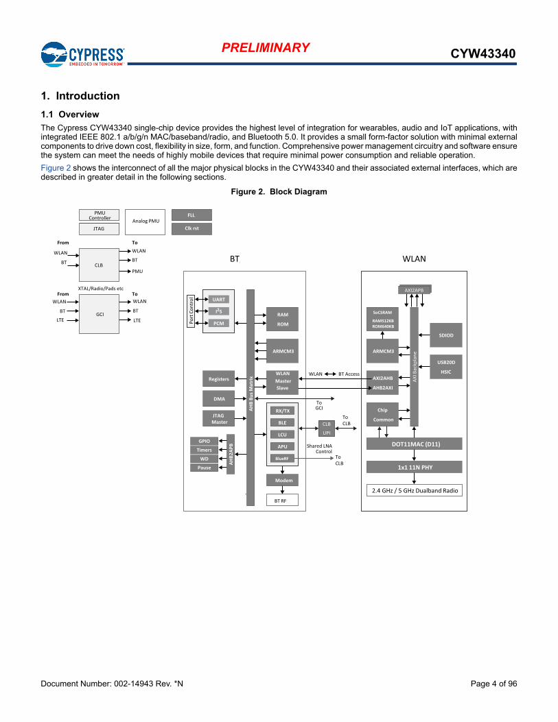
The Cypress CYW43340 single-chip device provides the highest level of integration for wearables, audio and IoT applications, withintegrated IEEE 802.1 a/b/g/n MAC/baseband/radio, and Bluetooth 5.0. It provides a small form-factor solution with minimal externalcomponents to drive down cost, flexibility in size, form, and function. Comprehensive power management circuitry and software ensurethe system can meet the needs of highly mobile devices that require minimal power consumption and reliable operation.
Figure 2 shows the interconnect of all the major physical blocks in the CYW43340 and their associated external interfaces, which aredescribed in greater detail in the following sections.
Figure 2. Block Diagram
Chip
Common
BT RF
Modem
AXI B
ackp
lane
ARMCM3
AXI2AHB
AHB2AXI
SDIOD
USB20D
HSIC
DOT11MAC (D11)
1x1 11N PHY
2.4 GHz / 5 GHz Dualband Radio
SoCSRAM
RAM512KB ROM640KB
AHB
Bus M
atrix
UART
ARMCM3
WLANMasterSlave
FMReceiver
RAM
ROM
I2S
PCMPort
Con
trol
RX/TX
LCU
APU
BlueRF
BLE
AXI2APB
DMA
JTAG Master
AHB2
APB
Timers
GPIO
WD
Pause
Registers
Shared LNA Control
WLAN BT Access
ARM CM0
RAM
ROM
SWP DIG
AHB Bridge
Analog PMUPMU
Controller
CLB
JTAG
From
WLAN
BT
ToWLAN
BT
PMU
XTAL/Radio/Pads etc
WLANBT/FM
GCI
FromWLAN
BT
ToWLAN
BT
FLL
Clk rst
To CLB
To CLB
ToGCI
LTE LTE
CLB
UPI
Document Number: 002-14943 Rev. *N Page 5 of 96
PRELIMINARY CYW43340
1.2 Features
The CYW43340 supports the following WLAN and Bluetooth features:
IEEE 802.11a/b/g/n dual-band radio with internal Power Amplifiers, LNAs, and T/R switches
Bluetooth 5.0 with integrated Class 1 PA
Concurrent Bluetooth, and WLAN operation
On-chip WLAN driver execution capable of supporting IEEE 802.11 functionality
Single- and dual-antenna support Single antenna with shared LNA Simultaneous BT/WLAN receive with single antenna
WLAN host interface options: SDIO v2.0, including default and high-speed timing. HSIC (USB device interface for short distance on-board applications)
BT host digital interface (can be used concurrently with above interfaces): UART (up to 4 Mbps)
ECI—enhanced coexistence support, ability to coordinate BT SCO transmissions around WLAN receives
I2S/PCM for BT audio
HCI high-speed UART (H4, H5) transport support
Wideband speech support (16 bits linear data, MSB first, left justified at 4K samples/s for transparent air coding, both through I2S and PCM interface)
Bluetooth SmartAudio® technology improves voice and music quality to headsets
Bluetooth low power inquiry and page scan
Bluetooth Low Energy (BLE) support
Bluetooth Packet Loss Concealment (PLC)
Bluetooth Wideband Speech (WBS)
Audio rate-matching algorithms
Multiple simultaneous A2DP audio stream
Document Number: 002-14943 Rev. *N Page 6 of 96
PRELIMINARY CYW43340
1.3 Standards Compliance
The CYW43340 supports the following standards:
Bluetooth 5.0 (including Bluetooth Low Energy)
IEEE 802.11n—Handheld Device Class (Section 11)
IEEE 802.11a
IEEE 802.11b
IEEE 802.11g
IEEE 802.11d
IEEE 802.11h
IEEE 802.11i
The CYW43340 will support the following future drafts/standards:
IEEE 802.11r—Fast Roaming (between APs)
IEEE 802.11k—Resource Management
IEEE 802.11w—Secure Management Frames
IEEE 802.11 Extensions: IEEE 802.11e QoS Enhancements (as per the WMM® specification is already supported) IEEE 802.11h 5 GHz Extensions IEEE 802.11i MAC Enhancements IEEE 802.11r Fast Roaming Support IEEE 802.11k Radio Resource Measurement
The CYW43340 supports the following security features and proprietary protocols:
Security: WEP WPA™ Personal WPA2™ Personal WMM WMM-PS (U-APSD) WMM-SA WAPI AES (Hardware Accelerator) TKIP (host-computed) CKIP (SW Support)
Proprietary Protocols: CCXv2 CCXv3 CCXv4 CCXv5
IEEE 802.15.2 Coexistence Compliance—on silicon solution compliant with IEEE 3 wire requirements
Document Number: 002-14943 Rev. *N Page 7 of 96
PRELIMINARY CYW43340
2. Power Supplies and Power Management
2.1 Power Supply Topology
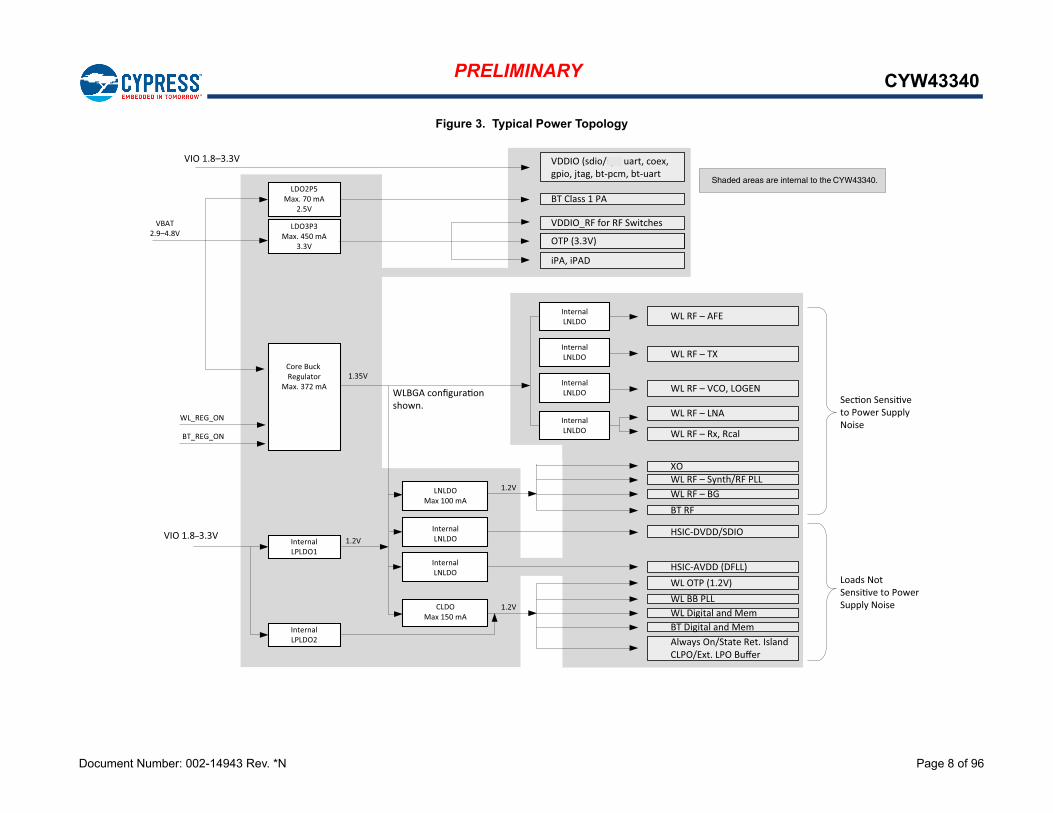
One Buck regulator, multiple LDO regulators, and a Power Management Unit (PMU) are integrated into the CYW43340. All regulatorsare programmable via the PMU. These blocks simplify power supply design for Bluetooth, and WLAN in embedded designs.
A single VBAT (2.9–4.8V) and VIO supply (1.8V to 3.3V) can be used, with all additional voltages being provided by the regulators inthe CYW43340.
Two control signals, BT_REG_ON and WL_REG_ON, are used to power-up the regulators and take the respective section out ofreset. The CBUCK CLDO and LNLDO power up when any of the reset signals are deasserted. All regulators are powered down onlywhen both BT_REG_ON and WL_REG_ON are deasserted. The CLDO and LNLDO may be turned off/on based on the dynamicdemands of the digital baseband.
The CYW43340 allows for an extremely low power-consumption mode by completely shutting down the CBUCK, CLDO, and LNDLOregulators. When in this state, LPLDO1 and LPLDO2 (which are low-power linear regulators that are supplied by the system VIOsupply) provide the CYW43340 with all the voltages it requires, further reducing leakage currents.
2.1.1 CYW43340 PMU Features
VBAT to 1.35Vout (372 mA maximum) Core-Buck (CBUCK) switching regulator
VBAT to 3.3Vout (450 mA maximum) LDO3P3 (external-capacitor)
VBAT to 2.5Vout (70 mA maximum) LDO2P5 (external-capacitor)
1.35V to 1.2Vout (100 mA maximum) LNLDO (external-capacitor)
1.35V to 1.2Vout (150 mA maximum) CLDO (external-capacitor)
1.35V to 1.2Vout (80 mA maximum) HSICDVDD LDO (external-capacitor)
Additional internal LDOs (not externally accessible)
Figure 3 on page 8 shows the regulators and a typical power topology.
Document Number: 002-14943 Rev. *N Page 8 of 96
PRELIMINARY CYW43340
Figure 3. Typical Power Topology
LNLDOMax 100 mA
CLDOMax 150 mA
InternalLNLDO
InternalLNLDO
InternalLNLDO
InternalLNLDO
VDDIO_RF for RF Switches
BT Class 1 PA
VIO 1.8–3.3V
OTP (3.3V)
1.2V
1.2V
1.35V
1.2V
Loads Not to Power
Supply Noise
to Power Supply Noise
Shaded areas are internal to the CYW43340.
VBAT2.9–4.8V
WL_REG_ON
BT_REG_ON
VIO 1.8–3.3V
WLBGA conshown.
InternalLNLDO
InternalLNLDO HSIC-AVDD (DFLL)
WL RF – AFE
WL RF – TX
WL RF – VCO, LOGEN
WL RF – LNA
WL RF – Rx, Rcal
FM LNA, MixerXOWL RF – Synth/RF PLL WL RF – BG
WL OTP (1.2V)
BT RF
WL BB PLLWL Digital and MemBT Digital and MemAlways On/State Ret. IslandCLPO/Ext. LPO Bu er
HSIC-DVDD/SDIO
VDDIO (sdio/spi, uart, coex,gpio, jtag, bt-pcm, bt-uart
OTP (3.3V)
iPA, iPAD
LDO2P5Max. 70 mA
2.5V
Core Buck Regulator
Max. 372 mA
InternalLPLDO1
InternalLPLDO2
LDO3P3Max. 450 mA
3.3V
Document Number: 002-14943 Rev. *N Page 9 of 96
PRELIMINARY CYW43340
2.2 WLAN Power Management
The CYW43340 has been designed with the stringent power consumption requirements of mobile devices in mind. All areas of thechip design are optimized to minimize power consumption. Silicon processes and cell libraries were chosen to reduce leakage currentand supply voltages. Additionally, the CYW43340 integrated RAM is a high Vt memory with dynamic clock control. The dominantsupply current consumed by the RAM is leakage current only. Additionally, the CYW43340 includes an advanced WLAN powermanagement unit (PMU) sequencer. The PMU sequencer provides significant power savings by putting the CYW43340 into variouspower management states appropriate to the current environment and activities that are being performed. The power managementunit enables and disables internal regulators, switches, and other blocks based on a computation of the required resources and atable that describes the relationship between resources and the time needed to enable and disable them. Power up sequences arefully programmable. Configurable, free-running counters (running at 32.768 kHz LPO clock) in the PMU sequencer are used to turnon/turn off individual regulators and power switches. Clock speeds are dynamically changed (or gated altogether) for the current mode.Slower clock speeds are used wherever possible.
The CYW43340 WLAN power states are described as follows:
Active mode— All WLAN blocks in the CYW43340 are powered up and fully functional with active carrier sensing and frame transmission and receiving. All required regulators are enabled and put in the most efficient mode based on the load current. Clock speeds are dynamically adjusted by the PMU sequencer.
Doze mode—The radio, analog domains, and most of the linear regulators are powered down. The rest of the CYW43340 remains powered up in an IDLE state. All main clocks (PLL, crystal oscillator or TCXO) are shut down to reduce active power to the minimum. The 32.768 kHz LPO clock is available only for the PMU sequencer. This condition is necessary to allow the PMU sequencer to wake up the chip and transition to Active mode. In Doze mode, the primary power consumed is due to leakage current.
Deep-sleep mode—Most of the chip including both analog and digital domains and most of the regulators are powered off. Logic states in the digital core are saved and preserved into a retention memory in the always-ON domain before the digital core is powered off. Upon a wake-up event triggered by the PMU timers, an external interrupt or a host resume through the HSIC or SDIO bus, logic states in the digital core are restored to their pre-deep-sleep settings to avoid lengthy HW re-initialization.
Power-down mode—The CYW43340 is effectively powered off by shutting down all internal regulators. The chip is brought out of this mode by external logic re-enabling the internal regulators.
2.3 PMU Sequencing
The PMU sequencer is responsible for minimizing system power consumption. It enables and disables various system resourcesbased on a computation of the required resources and a table that describes the relationship between resources and the time neededto enable and disable them.
Resource requests may come from several sources: clock requests from cores, the minimum resources defined in the Resource Minregister, and the resources requested by any active resource request timers. The PMU sequencer maps clock requests into a set ofresources required to produce the requested clocks.
Each resource is in one of four states: enabled, disabled, transition_on, and transition_off and has a timer that contains 0 when theresource is enabled or disabled and a non-zero value in the transition states. The timer is loaded with the time_on or time_off valueof the resource when the PMU determines that the resource must be enabled or disabled. That timer decrements on each 32.768 kHzPMU clock. When it reaches 0, the state changes from transition_off to disabled or transition_on to enabled. If the time_on value is0, the resource can go immediately from disabled to enabled. Similarly, a time_off value of 0 indicates that the resource can goimmediately from enabled to disabled. The terms enable sequence and disable sequence refer to either the immediate transition orthe timer load-decrement sequence.
During each clock cycle, the PMU sequencer performs the following actions:
1. Computes the required resource set based on requests and the resource dependency table.
2. Decrements all timers whose values are non zero. If a timer reaches 0, the PMU clears the ResourcePending bit for the resource and inverts the ResourceState bit.
3. Compares the request with the current resource status and determines which resources must be enabled or disabled.
4. Initiates a disable sequence for each resource that is enabled, no longer being requested, and has no powered up dependents.
5. Initiates an enable sequence for each resource that is disabled, is being requested, and has all of its dependencies enabled.
Document Number: 002-14943 Rev. *N Page 10 of 96
PRELIMINARY CYW43340
2.4 Power-Off Shutdown
The CYW43340 provides a low-power shutdown feature that allows the device to be turned off while the host, and any other devicesin the system, remain operational. When the CYW43340 is not needed in the system, VDDIO_RF and VDDC are shut down whileVDDIO remains powered. This allows the CYW43340 to be effectively off while keeping the I/O pins powered so that they do not drawextra current from any other devices connected to the I/O.
During a low-power shut-down state, provided VDDIO remains applied to the CYW43340, all outputs are tristated, and most inputssignals are disabled. Input voltages must remain within the limits defined for normal operation. This is done to prevent current pathsor create loading on any digital signals in the system, and enables the CYW43340 to be fully integrated in an embedded device andtake full advantage of the lowest power-savings modes.
Two signals on the CYW43340, the frequency reference input (WRF_XTAL_CAB_OP) and the LPO_IN input, are designed to be high-impedance inputs that do not load down the driving signal even if the chip does not have VDDIO power applied to it.
When the CYW43340 is powered on from this state, it is the same as a normal power-up and the device does not retain any informationabout its state from before it was powered down.
2.5 Power-Up/Power-Down/Reset Circuits
The CYW43340 has two signals (see Table 2) that enable or disable the Bluetooth and WLAN circuits and the internal regulator blocks, allowing the host to control power consumption. For timing diagrams of these signals and the required power-up sequences, see Section 19.: “Power-Up Sequence and Timing,” on page 87.
Table 2. Power-Up/Power-Down/Reset Control Signals
Signal Description
WL_REG_ON This signal is used by the PMU (with BT_REG_ON) to power up the WLAN section. It is also OR-gated with the BT_REG_ON input to control the internal CYW43340 regulators. When this pin is high, the regulators are enabled and the WLAN section is out of reset. When this pin is low, the WLAN section is in reset. If BT_REG_ON and WL_REG_ON are both low, the regulators are disabled. This pin has an internal 200 k pull-down resistor that is enabled by default. It can be disabled through programming.
BT_REG_ON This signal is used by the PMU (with WL_REG_ON) to decide whether or not to power down the internal CYW43340 regulators. If BT_REG_ON and WL_REG_ON are low, the regulators will be disabled. This pin has an internal 200 k pull-down resistor that is enabled by default. It can be disabled through programming.
Document Number: 002-14943 Rev. *N Page 11 of 96
PRELIMINARY CYW43340
3. Frequency References
An external crystal is used for generating all radio frequencies and normal operation clocking. As an alternative, an external frequencyreference driven by a temperature-compensated crystal oscillator (TCXO) signal may be used. In addition, a low-power oscillator(LPO) is provided for lower power mode timing.
Note: The crystal and TCXO implementations have different power supplies (WRF_XTAL_VDD1P2 for crystal,WRF_TCXO_VDD for TCXO).
3.1 Crystal Interface and Clock Generation
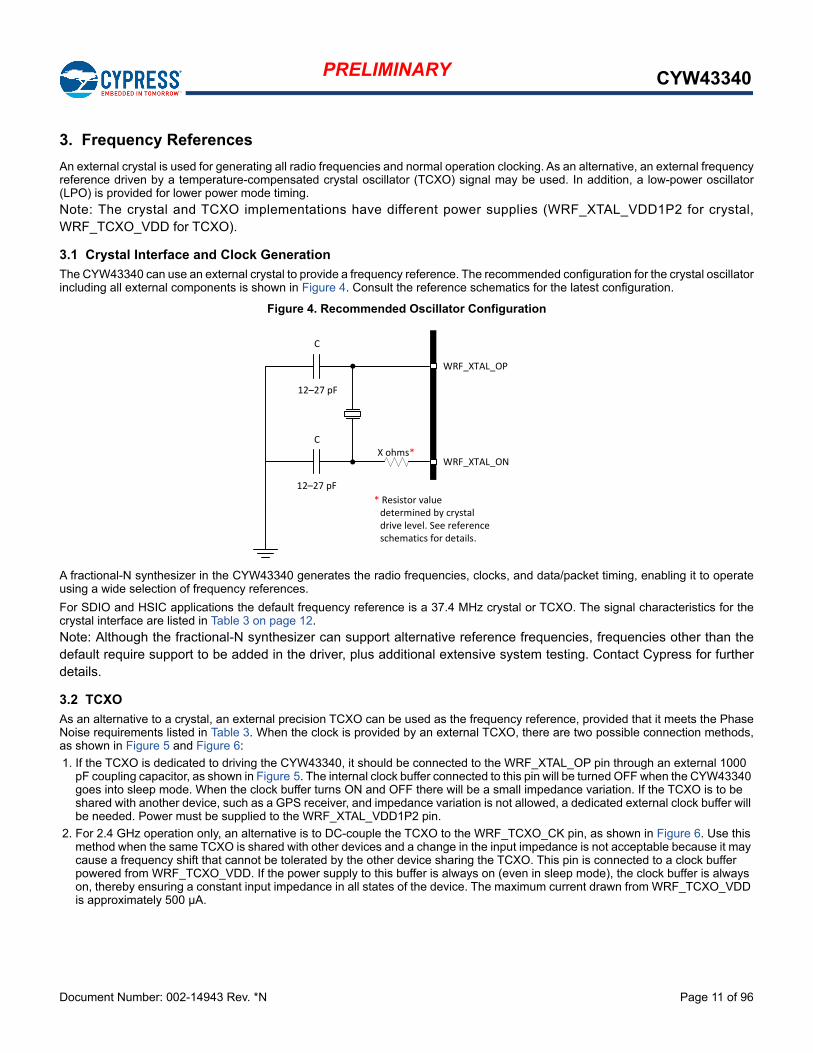
The CYW43340 can use an external crystal to provide a frequency reference. The recommended configuration for the crystal oscillatorincluding all external components is shown in Figure 4. Consult the reference schematics for the latest configuration.
Figure 4. Recommended Oscillator Configuration
A fractional-N synthesizer in the CYW43340 generates the radio frequencies, clocks, and data/packet timing, enabling it to operateusing a wide selection of frequency references.
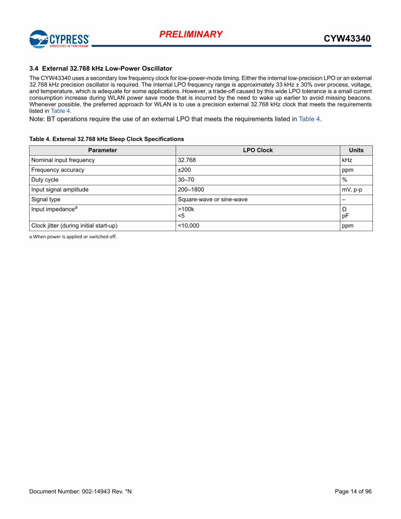
For SDIO and HSIC applications the default frequency reference is a 37.4 MHz crystal or TCXO. The signal characteristics for thecrystal interface are listed in Table 3 on page 12.
Note: Although the fractional-N synthesizer can support alternative reference frequencies, frequencies other than thedefault require support to be added in the driver, plus additional extensive system testing. Contact Cypress for furtherdetails.
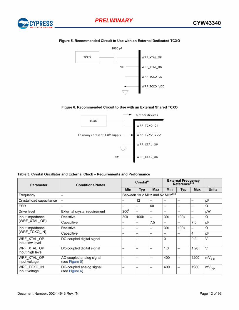
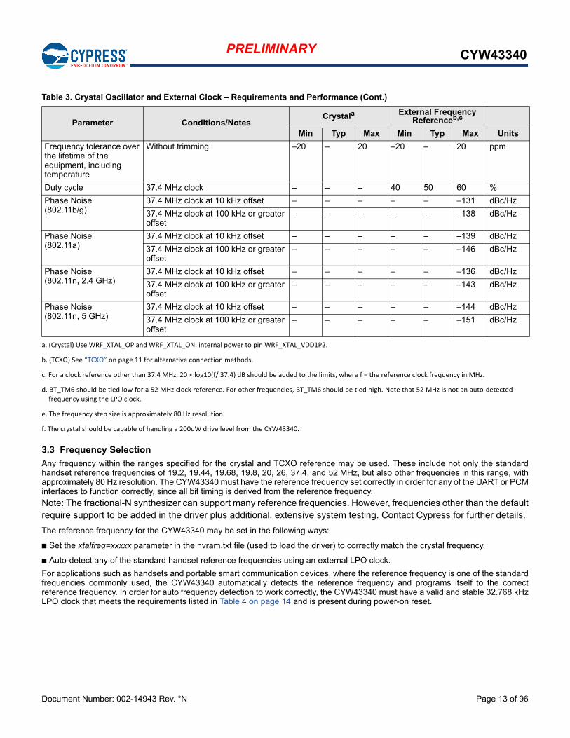
3.2 TCXO
As an alternative to a crystal, an external precision TCXO can be used as the frequency reference, provided that it meets the PhaseNoise requirements listed in Table 3. When the clock is provided by an external TCXO, there are two possible connection methods,as shown in Figure 5 and Figure 6:
1. If the TCXO is dedicated to driving the CYW43340, it should be connected to the WRF_XTAL_OP pin through an external 1000 pF coupling capacitor, as shown in Figure 5. The internal clock buffer connected to this pin will be turned OFF when the CYW43340 goes into sleep mode. When the clock buffer turns ON and OFF there will be a small impedance variation. If the TCXO is to be shared with another device, such as a GPS receiver, and impedance variation is not allowed, a dedicated external clock buffer will be needed. Power must be supplied to the WRF_XTAL_VDD1P2 pin.
2. For 2.4 GHz operation only, an alternative is to DC-couple the TCXO to the WRF_TCXO_CK pin, as shown in Figure 6. Use this method when the same TCXO is shared with other devices and a change in the input impedance is not acceptable because it may cause a frequency shift that cannot be tolerated by the other device sharing the TCXO. This pin is connected to a clock buffer powered from WRF_TCXO_VDD. If the power supply to this buffer is always on (even in sleep mode), the clock buffer is always on, thereby ensuring a constant input impedance in all states of the device. The maximum current drawn from WRF_TCXO_VDD is approximately 500 µA.
12–27 pF
12–27 pF
WRF_XTAL_ON
WRF_XTAL_OP
C
C
X ohms*
* Resistor value determined by crystal drive level. See reference schematics for details.
Document Number: 002-14943 Rev. *N Page 12 of 96
PRELIMINARY CYW43340
Figure 5. Recommended Circuit to Use with an External Dedicated TCXO
Figure 6. Recommended Circuit to Use with an External Shared TCXO
Table 3. Crystal Oscillator and External Clock – Requirements and Performance
Parameter Conditions/NotesCrystala External Frequency
Referenceb,c
Min Typ Max Min Typ Max Units
Frequency – Between 19.2 MHz and 52 MHzd,e
Crystal load capacitance – – 12 – – – – pF
ESR – – – 60 – – – Ω
Drive level External crystal requirement 200f – – – – – µW
Input impedance (WRF_XTAL_OP)
Resistive 30k 100k – 30k 100k – Ω
Capacitive – – 7.5 – – 7.5 pF
Input impedance (WRF_TCXO_IN)
Resistive – – – 30k 100k – Ω
Capacitive – – – – – 4 pF
WRF_XTAL_OP Input low level
DC-coupled digital signal – – – 0 – 0.2 V
WRF_XTAL_OPInput high level
DC-coupled digital signal – – – 1.0 – 1.26 V
WRF_XTAL_OP input voltage
AC-coupled analog signal(see Figure 5)
– – – 400 – 1200 mVp-p
WRF_TCXO_IN Input voltage
DC-coupled analog signal(see Figure 6)
– – – 400 – 1980 mVp-p
TCXO
NC
1000 pF
WRF_XTAL_OP
WRF_XTAL_ON
WRF_TCXO_CK
WRF_TCXO_VDD
TCXO
NC
WRF_TCXO_CK
WRF_XTAL_ON
WRF_XTAL_OP
To other devices
WRF_TCXO_VDDTo always present 1.8V supply
Document Number: 002-14943 Rev. *N Page 13 of 96
PRELIMINARY CYW43340
3.3 Frequency Selection
Any frequency within the ranges specified for the crystal and TCXO reference may be used. These include not only the standardhandset reference frequencies of 19.2, 19.44, 19.68, 19.8, 20, 26, 37.4, and 52 MHz, but also other frequencies in this range, withapproximately 80 Hz resolution. The CYW43340 must have the reference frequency set correctly in order for any of the UART or PCMinterfaces to function correctly, since all bit timing is derived from the reference frequency.
Note: The fractional-N synthesizer can support many reference frequencies. However, frequencies other than the defaultrequire support to be added in the driver plus additional, extensive system testing. Contact Cypress for further details.
The reference frequency for the CYW43340 may be set in the following ways:
Set the xtalfreq=xxxxx parameter in the nvram.txt file (used to load the driver) to correctly match the crystal frequency.
Auto-detect any of the standard handset reference frequencies using an external LPO clock.
For applications such as handsets and portable smart communication devices, where the reference frequency is one of the standardfrequencies commonly used, the CYW43340 automatically detects the reference frequency and programs itself to the correctreference frequency. In order for auto frequency detection to work correctly, the CYW43340 must have a valid and stable 32.768 kHzLPO clock that meets the requirements listed in Table 4 on page 14 and is present during power-on reset.
Frequency tolerance over the lifetime of the equipment, including temperature
Without trimming –20 – 20 –20 – 20 ppm
Duty cycle 37.4 MHz clock – – – 40 50 60 %
Phase Noise(802.11b/g)
37.4 MHz clock at 10 kHz offset – – – – – –131 dBc/Hz
37.4 MHz clock at 100 kHz or greater offset
– – – – – –138 dBc/Hz
Phase Noise(802.11a)
37.4 MHz clock at 10 kHz offset – – – – – –139 dBc/Hz
37.4 MHz clock at 100 kHz or greater offset
– – – – – –146 dBc/Hz
Phase Noise(802.11n, 2.4 GHz)
37.4 MHz clock at 10 kHz offset – – – – – –136 dBc/Hz
37.4 MHz clock at 100 kHz or greater offset
– – – – – –143 dBc/Hz
Phase Noise(802.11n, 5 GHz)
37.4 MHz clock at 10 kHz offset – – – – – –144 dBc/Hz
37.4 MHz clock at 100 kHz or greater offset
– – – – – –151 dBc/Hz
a. (Crystal) Use WRF_XTAL_OP and WRF_XTAL_ON, internal power to pin WRF_XTAL_VDD1P2.
b. (TCXO) See “TCXO” on page 11 for alternative connection methods.
c. For a clock reference other than 37.4 MHz, 20 × log10(f/ 37.4) dB should be added to the limits, where f = the reference clock frequency in MHz.
d. BT_TM6 should be tied low for a 52 MHz clock reference. For other frequencies, BT_TM6 should be tied high. Note that 52 MHz is not an auto-detected
frequency using the LPO clock.
e. The frequency step size is approximately 80 Hz resolution.
f. The crystal should be capable of handling a 200uW drive level from the CYW43340.
Table 3. Crystal Oscillator and External Clock – Requirements and Performance (Cont.)
Parameter Conditions/NotesCrystala External Frequency
Referenceb,c
Min Typ Max Min Typ Max Units
Document Number: 002-14943 Rev. *N Page 14 of 96
PRELIMINARY CYW43340
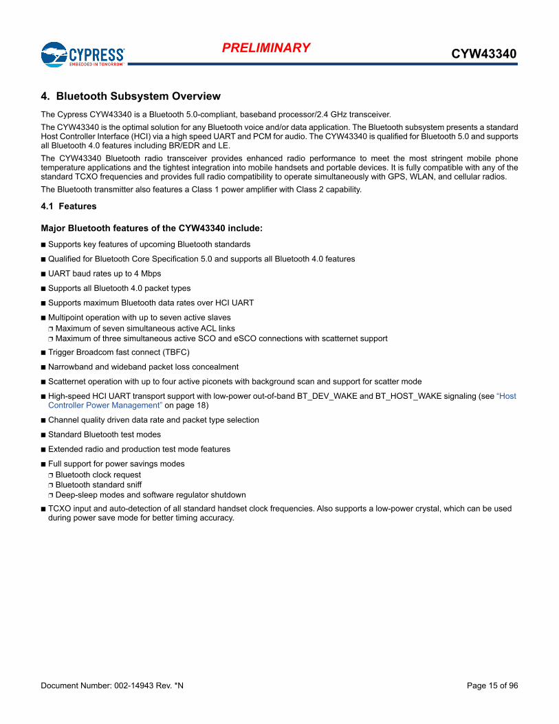
3.4 External 32.768 kHz Low-Power Oscillator
The CYW43340 uses a secondary low frequency clock for low-power-mode timing. Either the internal low-precision LPO or an external32.768 kHz precision oscillator is required. The internal LPO frequency range is approximately 33 kHz ± 30% over process, voltage,and temperature, which is adequate for some applications. However, a trade-off caused by this wide LPO tolerance is a small currentconsumption increase during WLAN power save mode that is incurred by the need to wake up earlier to avoid missing beacons.Whenever possible, the preferred approach for WLAN is to use a precision external 32.768 kHz clock that meets the requirementslisted in Table 4.
Note: BT operations require the use of an external LPO that meets the requirements listed in Table 4.
Table 4. External 32.768 kHz Sleep Clock Specifications
Parameter LPO Clock Units
Nominal input frequency 32.768 kHz
Frequency accuracy ±200 ppm
Duty cycle 30–70 %
Input signal amplitude 200–1800 mV, p-p
Signal type Square-wave or sine-wave –
Input impedancea
a.When power is applied or switched off.
>100k<5
ΩpF
Clock jitter (during initial start-up) <10,000 ppm
Document Number: 002-14943 Rev. *N Page 15 of 96
PRELIMINARY CYW43340
4. Bluetooth Subsystem Overview
The Cypress CYW43340 is a Bluetooth 5.0-compliant, baseband processor/2.4 GHz transceiver.
The CYW43340 is the optimal solution for any Bluetooth voice and/or data application. The Bluetooth subsystem presents a standardHost Controller Interface (HCI) via a high speed UART and PCM for audio. The CYW43340 is qualified for Bluetooth 5.0 and supportsall Bluetooth 4.0 features including BR/EDR and LE.
The CYW43340 Bluetooth radio transceiver provides enhanced radio performance to meet the most stringent mobile phonetemperature applications and the tightest integration into mobile handsets and portable devices. It is fully compatible with any of thestandard TCXO frequencies and provides full radio compatibility to operate simultaneously with GPS, WLAN, and cellular radios.
The Bluetooth transmitter also features a Class 1 power amplifier with Class 2 capability.
4.1 Features
Major Bluetooth features of the CYW43340 include:
Supports key features of upcoming Bluetooth standards
Qualified for Bluetooth Core Specification 5.0 and supports all Bluetooth 4.0 features
UART baud rates up to 4 Mbps
Supports all Bluetooth 4.0 packet types
Supports maximum Bluetooth data rates over HCI UART
Multipoint operation with up to seven active slaves Maximum of seven simultaneous active ACL links Maximum of three simultaneous active SCO and eSCO connections with scatternet support
Trigger Broadcom fast connect (TBFC)
Narrowband and wideband packet loss concealment
Scatternet operation with up to four active piconets with background scan and support for scatter mode
High-speed HCI UART transport support with low-power out-of-band BT_DEV_WAKE and BT_HOST_WAKE signaling (see “Host Controller Power Management” on page 18)
Channel quality driven data rate and packet type selection
Standard Bluetooth test modes
Extended radio and production test mode features
Full support for power savings modes Bluetooth clock request Bluetooth standard sniff Deep-sleep modes and software regulator shutdown
TCXO input and auto-detection of all standard handset clock frequencies. Also supports a low-power crystal, which can be used during power save mode for better timing accuracy.
Document Number: 002-14943 Rev. *N Page 16 of 96
PRELIMINARY CYW43340
4.2 Bluetooth Radio
The CYW43340 has an integrated radio transceiver that has been optimized for use in 2.4 GHz Bluetooth wireless systems. It hasbeen designed to provide low-power, low-cost, robust communications for applications operating in the globally available 2.4 GHzunlicensed ISM band. It is fully compliant with the Bluetooth Radio Specification and EDR specification and meets or exceeds therequirements to provide the highest communication link quality of service.
4.2.1 Transmit
The CYW43340 features a fully integrated zero-IF transmitter. The baseband transmit data is GFSK-modulated in the modem blockand upconverted to the 2.4 GHz ISM band in the transmitter path. The transmitter path consists of signal filtering, I/Q upconversion,output power amplifier, and RF filtering. The transmitter path also incorporates /4–DQPSK for 2 Mbps and 8–DPSK for 3 Mbps tosupport EDR. The transmitter section is compatible to the Bluetooth Low Energy specification. The transmitter PA bias can also beadjusted to provide Bluetooth class 1 or class 2 operation.
4.2.2 Digital Modulator
The digital modulator performs the data modulation and filtering required for the GFSK, /4–DQPSK, and 8–DPSK signal. The fullydigital modulator minimizes any frequency drift or anomalies in the modulation characteristics of the transmitted signal and is muchmore stable than direct VCO modulation schemes.
4.2.3 Digital Demodulator and Bit Synchronizer
The digital demodulator and bit synchronizer take the low-IF received signal and perform an optimal frequency tracking and bit-synchronization algorithm.
4.2.4 Power Amplifier
The fully integrated PA supports Class 1 or Class 2 output using a highly linearized, temperature-compensated design. This providesgreater flexibility in front-end matching and filtering. Due to the linear nature of the PA combined with some integrated filtering, externalfiltering is required to meet the Bluetooth and regulatory harmonic and spurious requirements. For integrated mobile handset appli-cations in which Bluetooth is integrated next to the cellular radio, external filtering can be applied to achieve near thermal noise levelsfor spurious and radiated noise emissions. The transmitter features a sophisticated on-chip transmit signal strength indicator (TSSI)block to keep the absolute output power variation within a tight range across process, voltage, and temperature.
4.2.5 Receiver
The receiver path uses a low-IF scheme to downconvert the received signal for demodulation in the digital demodulator and bitsynchronizer. The receiver path provides a high degree of linearity, an extended dynamic range, and high-order on-chip channelfiltering to ensure reliable operation in the noisy 2.4 GHz ISM band. The front-end topology with built-in out-of-band attenuationenables the CYW43340 to be used in most applications with minimal off-chip filtering. For integrated handset operation, in which theBluetooth function is integrated close to the cellular transmitter, external filtering is required to eliminate the desensitization of thereceiver by the cellular transmit signal.
4.2.6 Digital Demodulator and Bit Synchronizer
The digital demodulator and bit synchronizer take the low-IF received signal and perform an optimal frequency tracking and bitsynchronization algorithm.
4.2.7 Receiver Signal Strength Indicator
The radio portion of the CYW43340 provides a Receiver Signal Strength Indicator (RSSI) signal to the baseband, so that the controllercan take part in a Bluetooth power-controlled link by providing a metric of its own receiver signal strength to determine whether thetransmitter should increase or decrease its output power.
4.2.8 Local Oscillator Generation
Local Oscillator (LO) generation provides fast frequency hopping (1600 hops/second) across the 79 maximum available channels.The LO generation subblock employs an architecture for high immunity to LO pulling during PA operation. The CYW43340 uses aninternal RF and IF loop filter.
4.2.9 Calibration
The CYW43340 radio transceiver features an automated calibration scheme that is fully self contained in the radio. No user interactionis required during normal operation or during manufacturing to provide the optimal performance. Calibration optimizes the perfor-mance of all the major blocks within the radio to within 2% of optimal conditions, including gain and phase characteristics of filters,matching between key components, and key gain blocks. This takes into account process variation and temperature variation.Calibration occurs transparently during normal operation during the settling time of the hops and calibrates for temperature variationsas the device cools and heats during normal operation in its environment.
Document Number: 002-14943 Rev. *N Page 17 of 96
PRELIMINARY CYW43340
5. Bluetooth Baseband Core
The Bluetooth Baseband Core (BBC) implements all of the time critical functions required for high-performance Bluetooth operation.The BBC manages the buffering, segmentation, and routing of data for all connections. It also buffers data that passes through it,handles data flow control, schedules SCO/ACL TX/RX transactions, monitors Bluetooth slot usage, optimally segments and packagesdata into baseband packets, manages connection status indicators, and composes and decodes HCI packets. In addition to thesefunctions, it independently handles HCI event types, and HCI command types.
The following transmit and receive functions are also implemented in the BBC hardware to increase reliability and security of the TX/RX data before sending over the air:
Symbol timing recovery, data deframing, forward error correction (FEC), header error control (HEC), cyclic redundancy check (CRC), data decryption, and data dewhitening in the receiver.
Data framing, FEC generation, HEC generation, CRC generation, key generation, data encryption, and data whitening in the transmitter.
5.1 Bluetooth 5.0 Features
The BBC is qualified for Bluetooth Core Specification 5.0 and supports all Bluetooth 4.0 features, with the following benefits:
Dual-mode classic Bluetooth and classic Low Energy (BT and BLE) operation.
Low Energy Physical Layer
Low Energy Link Layer
Enhancements to HCI for Low Energy
Low Energy Direct Test mode
AES encryption
Note: The CYW43340 is compatible with the Bluetooth Low Energy operating mode, which provides a dramaticreduction in the power consumption of the Bluetooth radio and baseband. The primary application for this mode is toprovide support for low data rate devices, such as sensors and remote controls.
5.2 Link Control Layer
The link control layer is part of the Bluetooth link control functions that are implemented in dedicated logic in the link control unit (LCU).This layer consists of the command controller that takes commands from the software, and other controllers that are activated orconfigured by the command controller, to perform the link control tasks. Each task performs a different state in the Bluetooth LinkController.
Major states: Standby Connection
Substates: Page Page Scan Inquiry Inquiry Scan Sniff BLE Adv BLE Scan/Initiation
5.3 Test Mode Support
The CYW43340 fully supports Bluetooth Test mode as described in Part I:1 of the Specification of the Bluetooth System Version 3.0.This includes the transmitter tests, normal and delayed loopback tests, and reduced hopping sequence.
In addition to the standard Bluetooth Test Mode, the CYW43340 also supports enhanced testing features to simplify RF debuggingand qualification and type-approval testing. These features include:
Fixed frequency carrier wave (unmodulated) transmission Simplifies some type-approval measurements (Japan) Aids in transmitter performance analysis
Document Number: 002-14943 Rev. *N Page 18 of 96
PRELIMINARY CYW43340
Fixed frequency constant receiver mode Receiver output directed to I/O pin Allows for direct BER measurements using standard RF test equipment Facilitates spurious emissions testing for receive mode
Fixed frequency constant transmission Eight-bit fixed pattern or PRBS-9 Enables modulated signal measurements with standard RF test equipment
5.4 Bluetooth Power Management Unit
The Bluetooth Power Management Unit (PMU) provides power management features that can be invoked by either software throughpower management registers or packet handling in the baseband core. The power management functions provided by the CYW43340are:
RF Power Management
Host Controller Power Management
BBC Power Management
5.4.1 RF Power Management
The BBC generates power-down control signals for the transmit path, receive path, PLL, and power amplifier to the 2.4 GHz trans-ceiver. The transceiver then processes the power-down functions accordingly.
5.4.2 Host Controller Power Management
When running in UART mode, the CYW43340 may be configured so that dedicated signals are used for power management hand-shaking between the CYW43340 and the host. The basic power saving functions supported by those hand-shaking signals includethe standard Bluetooth defined power savings modes and standby modes of operation.
Table 5 describes the power-control hand-shake signals used with the UART interface.
Table 5. Power Control Pin Description
Signal Type Description
BT_DEV_WAKE I Bluetooth device wake-up: Signal from the host to the CYW43340 indicating that the host requires attention.
Asserted: The Bluetooth device must wake-up or remain awake.
Deasserted: The Bluetooth device may sleep when sleep criteria are met.The polarity of this signal is software configurable and can be asserted high or low.
BT_HOST_WAKE O Host wake up. Signal from the CYW43340 to the host indicating that the CYW43340 requires attention.
Asserted: host device must wake-up or remain awake.
Deasserted: host device may sleep when sleep criteria are met.The polarity of this signal is software configurable and can be asserted high or low.
CLK_REQ O The CYW43340 asserts CLK_REQ when Bluetooth, or WLAN directs the host to turn on the reference clock. The CLK_REQ polarity is active-high. Add an external 100 kΩ pull-down resistor to ensure the signal is deasserted when the CYW43340 powers up or resets when VDDIO is present.
Note: Pad function Control Register is set to 0 for these pins.
Document Number: 002-14943 Rev. *N Page 19 of 96
PRELIMINARY CYW43340
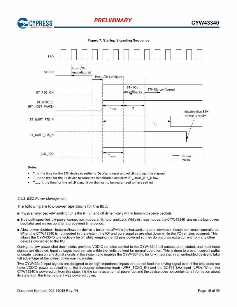
Figure 7. Startup Signaling Sequence
5.4.3 BBC Power Management
The following are low-power operations for the BBC:
Physical layer packet-handling turns the RF on and off dynamically within transmit/receive packets.
Bluetooth-specified low-power connection modes: sniff, hold, and park. While in these modes, the CYW43340 runs on the low-power oscillator and wakes up after a predefined time period.
A low-power shutdown feature allows the device to be turned off while the host and any other devices in the system remain operational. When the CYW43340 is not needed in the system, the RF and core supplies are shut down while the I/O remains powered. This allows the CYW43340 to effectively be off while keeping the I/O pins powered so they do not draw extra current from any other devices connected to the I/O.
During the low-power shut-down state, provided VDDIO remains applied to the CYW43340, all outputs are tristated, and most inputsignals are disabled. Input voltages must remain within the limits defined for normal operation. This is done to prevent current pathsor create loading on any digital signals in the system and enables the CYW43340 to be fully integrated in an embedded device to takefull advantage of the lowest power-saving modes.
Two CYW43340 input signals are designed to be high-impedance inputs that do not load the driving signal even if the chip does nothave VDDIO power supplied to it: the frequency reference input (WRF_TCXO_IN) and the 32.768 kHz input (LPO). When theCYW43340 is powered on from this state, it is the same as a normal power-up, and the device does not contain any information aboutits state from the time before it was powered down.
VDDIO
LPO
BT_UART_RTS_N
CLK_REQ
BT_GPIO_1 (BT_HOST_WAKE)
BT_REG_ON
BT_UART_CTS_N
Host I/Os
Host I/Os con
BTH IOs BTH IOs nco
T 2
T
T
T 1
T 1 is fo BTH to its IOs a a aps .T 2 is fo BT to t on BT_UART_RTS_N T is th fo f c si a th host to b a a to ha .
D i nP
i that BTH ic is .
Document Number: 002-14943 Rev. *N Page 20 of 96
PRELIMINARY CYW43340
5.4.4 Wideband Speech
The CYW43340 provides support for wideband speech (WBS) using on-chip Smart Audio technology. The CYW43340 can performsubband-codec (SBC), as well as mSBC, encoding and decoding of linear 16 bits at 16 kHz (256 Kbps rate) transferred over the PCMbus.
5.4.5 Packet Loss Concealment
Packet Loss Concealment (PLC) improves apparent audio quality for systems with marginal link performance. Bluetooth messagesare sent in packets. When a packet is lost, it creates a gap in the received audio bit-stream. Packet loss can be mitigated in severalways:
Fill in zeros.
Ramp down the output audio signal toward zero (this is the method used in current Bluetooth headsets).
Repeat the last frame (or packet) of the received bit-stream and decode it as usual (frame repeat).
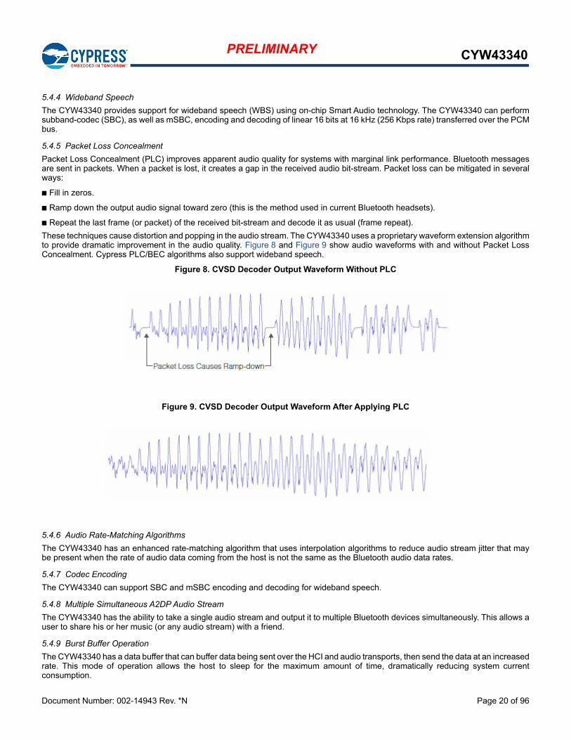
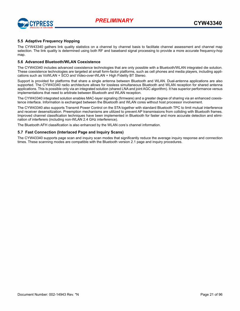
These techniques cause distortion and popping in the audio stream. The CYW43340 uses a proprietary waveform extension algorithmto provide dramatic improvement in the audio quality. Figure 8 and Figure 9 show audio waveforms with and without Packet LossConcealment. Cypress PLC/BEC algorithms also support wideband speech.
Figure 8. CVSD Decoder Output Waveform Without PLC
Figure 9. CVSD Decoder Output Waveform After Applying PLC
5.4.6 Audio Rate-Matching Algorithms
The CYW43340 has an enhanced rate-matching algorithm that uses interpolation algorithms to reduce audio stream jitter that maybe present when the rate of audio data coming from the host is not the same as the Bluetooth audio data rates.
5.4.7 Codec Encoding
The CYW43340 can support SBC and mSBC encoding and decoding for wideband speech.
5.4.8 Multiple Simultaneous A2DP Audio Stream
The CYW43340 has the ability to take a single audio stream and output it to multiple Bluetooth devices simultaneously. This allows auser to share his or her music (or any audio stream) with a friend.
5.4.9 Burst Buffer Operation
The CYW43340 has a data buffer that can buffer data being sent over the HCI and audio transports, then send the data at an increasedrate. This mode of operation allows the host to sleep for the maximum amount of time, dramatically reducing system currentconsumption.
Document Number: 002-14943 Rev. *N Page 21 of 96
PRELIMINARY CYW43340
5.5 Adaptive Frequency Hopping
The CYW43340 gathers link quality statistics on a channel by channel basis to facilitate channel assessment and channel mapselection. The link quality is determined using both RF and baseband signal processing to provide a more accurate frequency-hopmap.
5.6 Advanced Bluetooth/WLAN Coexistence
The CYW43340 includes advanced coexistence technologies that are only possible with a Bluetooth/WLAN integrated die solution.These coexistence technologies are targeted at small form-factor platforms, such as cell phones and media players, including appli-cations such as VoWLAN + SCO and Video-over-WLAN + High Fidelity BT Stereo.
Support is provided for platforms that share a single antenna between Bluetooth and WLAN. Dual-antenna applications are alsosupported. The CYW43340 radio architecture allows for lossless simultaneous Bluetooth and WLAN reception for shared antennaapplications. This is possible only via an integrated solution (shared LNA and joint AGC algorithm). It has superior performance versusimplementations that need to arbitrate between Bluetooth and WLAN reception.
The CYW43340 integrated solution enables MAC-layer signaling (firmware) and a greater degree of sharing via an enhanced coexis-tence interface. Information is exchanged between the Bluetooth and WLAN cores without host processor involvement.
The CYW43340 also supports Transmit Power Control on the STA together with standard Bluetooth TPC to limit mutual interferenceand receiver desensitization. Preemption mechanisms are utilized to prevent AP transmissions from colliding with Bluetooth frames.Improved channel classification techniques have been implemented in Bluetooth for faster and more accurate detection and elimi-nation of interferers (including non-WLAN 2.4 GHz interference).
The Bluetooth AFH classification is also enhanced by the WLAN core’s channel information.
5.7 Fast Connection (Interlaced Page and Inquiry Scans)
The CYW43340 supports page scan and inquiry scan modes that significantly reduce the average inquiry response and connectiontimes. These scanning modes are compatible with the Bluetooth version 2.1 page and inquiry procedures.
Document Number: 002-14943 Rev. *N Page 22 of 96
PRELIMINARY CYW43340
6. Microprocessor and Memory Unit for Bluetooth
The Bluetooth microprocessor core is based on the ARM® Cortex™-M3 32-bit RISC processor with embedded ICE-RT debug andJTAG interface units. It runs software from the link control (LC) layer, up to the host controller interface (HCI).
The ARM core is paired with a memory unit that contains 652 KB of ROM memory for program storage and boot ROM, 195 KB ofRAM for data scratchpad and patch RAM code. The internal ROM allows for flexibility during power-on reset to enable the same deviceto be used in various configurations. At power-up, the lower-layer protocol stack is executed from the internal ROM memory.
External patches may be applied to the ROM-based firmware to provide flexibility for bug fixes or features additions. These patchesmay be downloaded from the host to the CYW43340 through the UART transports. The mechanism for downloading via UART isidentical to the proven interface of the CYW4329 and CYW4330 devices.
6.1 RAM, ROM, and Patch Memory
The CYW43340 Bluetooth core has 195 KB of internal RAM which is mapped between general purpose scratch pad memory andpatch memory and 652 KB of ROM used for the lower-layer protocol stack, test mode software, and boot ROM. The patch memorycapability enables the addition of code changes for purposes of feature additions and bug fixes to the ROM memory.
6.2 Reset
The CYW43340 has an integrated power-on reset circuit that resets all circuits to a known power-on state. The BT power-on reset(POR) circuit is out of reset after BT_REG_ON goes High. If BT_REG_ON is low, then the POR circuit is held in reset.
Document Number: 002-14943 Rev. *N Page 23 of 96
PRELIMINARY CYW43340
7. Bluetooth Peripheral Transport Unit
7.1 PCM Interface
The CYW43340 supports two independent PCM interfaces that share the pins with the I2S interfaces. The PCM Interface on theCYW43340 can connect to linear PCM Codec devices in master or slave mode. In master mode, the CYW43340 generates thePCM_CLK and PCM_SYNC signals, and in slave mode, these signals are provided by another master on the PCM interface and areinputs to the CYW43340. The configuration of the PCM interface may be adjusted by the host through the use of vendor-specific HCIcommands.
7.1.1 Slot Mapping
The CYW43340 supports up to three simultaneous full-duplex SCO or eSCO channels through the PCM interface. These threechannels are time-multiplexed onto the single PCM interface by using a time-slotting scheme where the 8 kHz or 16 kHz audio sampleinterval is divided into as many as 16 slots. The number of slots is dependent on the selected interface rate of 128 kHz, 512 kHz, or1024 kHz. The corresponding number of slots for these interface rate is 1, 2, 4, 8, and 16, respectively. Transmit and receive PCMdata from an SCO channel is always mapped to the same slot. The PCM data output driver tristates its output on unused slots to allowother devices to share the same PCM interface signals. The data output driver tristates its output after the falling edge of the PCMclock during the last bit of the slot.
7.1.2 Frame Synchronization
The CYW43340 supports both short- and long-frame synchronization in both master and slave modes. In short-frame synchronizationmode, the frame synchronization signal is an active-high pulse at the audio frame rate that is a single-bit period in width and issynchronized to the rising edge of the bit clock. The PCM slave looks for a high on the falling edge of the bit clock and expects thefirst bit of the first slot to start at the next rising edge of the clock. In long-frame synchronization mode, the frame synchronizationsignal is again an active-high pulse at the audio frame rate; however, the duration is three bit periods and the pulse starts coincidentwith the first bit of the first slot.
7.1.3 Data Formatting
The CYW43340 may be configured to generate and accept several different data formats. For conventional narrowband speech mode,the CYW43340 uses 13 of the 16 bits in each PCM frame. The location and order of these 13 bits can be configured to support variousdata formats on the PCM interface. The remaining three bits are ignored on the input and may be filled with 0s, 1s, a sign bit, or aprogrammed value on the output. The default format is 13-bit 2’s complement data, left justified, and clocked MSB first.
7.1.4 Wideband Speech Support
When the host encodes Wideband Speech (WBS) packets in transparent mode, the encoded packets are transferred over the PCMbus for an eSCO voice connection. In this mode, the PCM bus is typically configured in master mode for a 4 kHz sync rate with 16-bit samples, resulting in a 64 kbps bit rate. The CYW43340 also supports slave transparent mode using a proprietary rate-matchingscheme. In SBC-code mode, linear 16-bit data at 16 kHz (256 kbps rate) is transferred over the PCM bus.
7.1.5 Burst PCM Mode
In this mode of operation, the PCM bus runs at a significantly higher rate of operation to allow the host to duty cycle its operation andsave current. In this mode of operation, the PCM bus can operate at a rate of up to 24 MHz. This mode of operation is initiated withan HCI command from the host.
Document Number: 002-14943 Rev. *N Page 24 of 96
PRELIMINARY CYW43340
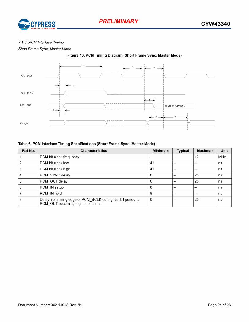
7.1.6 PCM Interface Timing
Short Frame Sync, Master Mode
Figure 10. PCM Timing Diagram (Short Frame Sync, Master Mode)
Table 6. PCM Interface Timing Specifications (Short Frame Sync, Master Mode)
Ref No. Characteristics Minimum Typical Maximum Unit
1 PCM bit clock frequency – – 12 MHz
2 PCM bit clock low 41 – – ns
3 PCM bit clock high 41 – – ns
4 PCM_SYNC delay 0 – 25 ns
5 PCM_OUT delay 0 – 25 ns
6 PCM_IN setup 8 – – ns
7 PCM_IN hold 8 – – ns
8 Delay from rising edge of PCM_BCLK during last bit period to PCM_OUT becoming high impedance
0 – 25 ns
PCM_BCLK
PCM_SYNC
PCM_OUT
12 3
4
5
PCM_IN
6
8
HIGH IMPEDANCE
7
Document Number: 002-14943 Rev. *N Page 25 of 96
PRELIMINARY CYW43340
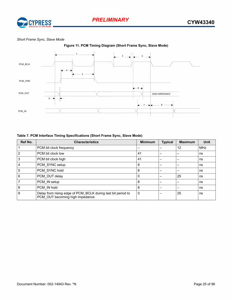
Short Frame Sync, Slave Mode
Figure 11. PCM Timing Diagram (Short Frame Sync, Slave Mode)
Table 7. PCM Interface Timing Specifications (Short Frame Sync, Slave Mode)
Ref No. Characteristics Minimum Typical Maximum Unit
1 PCM bit clock frequency – – 12 MHz
2 PCM bit clock low 41 – – ns
3 PCM bit clock high 41 – – ns
4 PCM_SYNC setup 8 – – ns
5 PCM_SYNC hold 8 – – ns
6 PCM_OUT delay 0 – 25 ns
7 PCM_IN setup 8 – – ns
8 PCM_IN hold 8 – – ns
9 Delay from rising edge of PCM_BCLK during last bit period to PCM_OUT becoming high impedance
0 – 25 ns
PCM_BCLK
PCM_SYNC
PCM_OUT
12 3
4
5
6
PCM_IN
7
9
HIGH IMPEDANCE
8
Document Number: 002-14943 Rev. *N Page 26 of 96
PRELIMINARY CYW43340
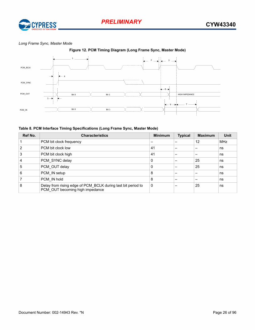
Long Frame Sync, Master Mode
Figure 12. PCM Timing Diagram (Long Frame Sync, Master Mode)
Table 8. PCM Interface Timing Specifications (Long Frame Sync, Master Mode)
Ref No. Characteristics Minimum Typical Maximum Unit
1 PCM bit clock frequency – – 12 MHz
2 PCM bit clock low 41 – – ns
3 PCM bit clock high 41 – – ns
4 PCM_SYNC delay 0 – 25 ns
5 PCM_OUT delay 0 – 25 ns
6 PCM_IN setup 8 – – ns
7 PCM_IN hold 8 – – ns
8 Delay from rising edge of PCM_BCLK during last bit period to PCM_OUT becoming high impedance
0 – 25 ns
PCM_BCLK
PCM_SYNC
PCM_OUT
12 3
4
5
PCM_IN
6
8
HIGH IMPEDANCE
7
Bit 0
Bit 0
Bit 1
Bit 1
Document Number: 002-14943 Rev. *N Page 27 of 96
PRELIMINARY CYW43340
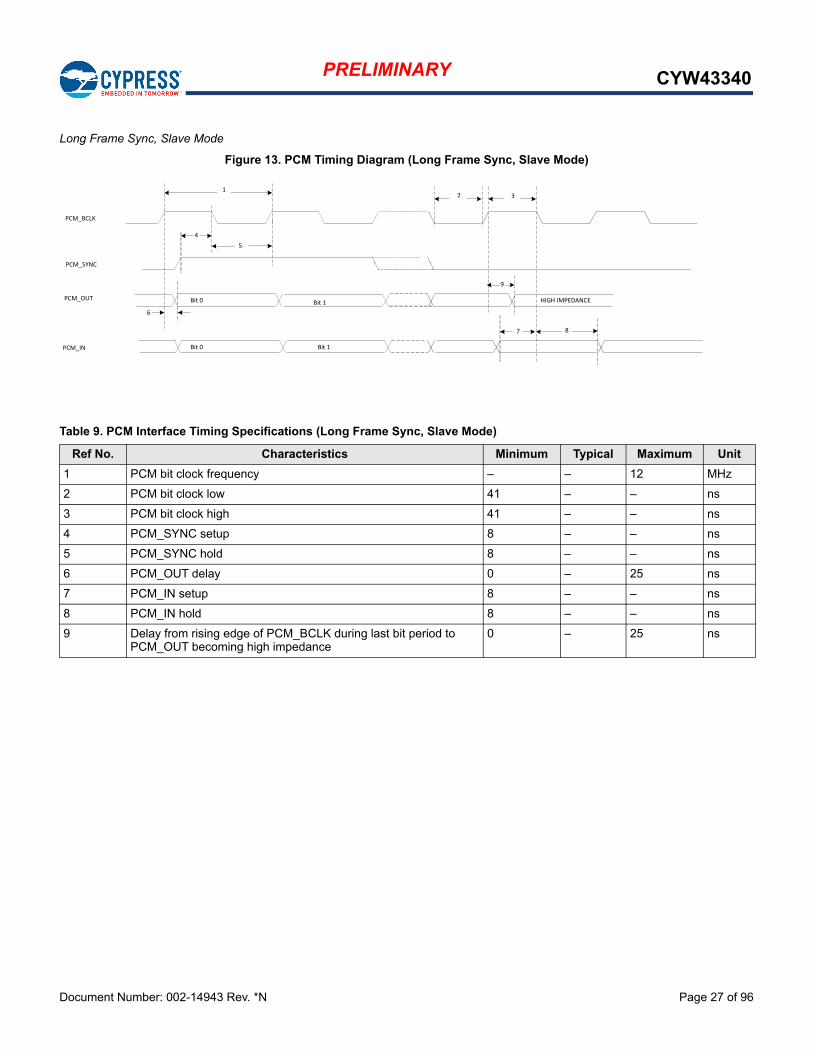
Long Frame Sync, Slave Mode
Figure 13. PCM Timing Diagram (Long Frame Sync, Slave Mode)
Table 9. PCM Interface Timing Specifications (Long Frame Sync, Slave Mode)
Ref No. Characteristics Minimum Typical Maximum Unit
1 PCM bit clock frequency – – 12 MHz
2 PCM bit clock low 41 – – ns
3 PCM bit clock high 41 – – ns
4 PCM_SYNC setup 8 – – ns
5 PCM_SYNC hold 8 – – ns
6 PCM_OUT delay 0 – 25 ns
7 PCM_IN setup 8 – – ns
8 PCM_IN hold 8 – – ns
9 Delay from rising edge of PCM_BCLK during last bit period to PCM_OUT becoming high impedance
0 – 25 ns
PCM_BCLK
PCM_SYNC
PCM_OUT
12 3
4
5
6
PCM_IN
7
9
HIGH IMPEDANCE
8
Bit 0
Bit 0
Bit 1
Bit 1
Document Number: 002-14943 Rev. *N Page 28 of 96
PRELIMINARY CYW43340
Short Frame Sync, Burst Mode
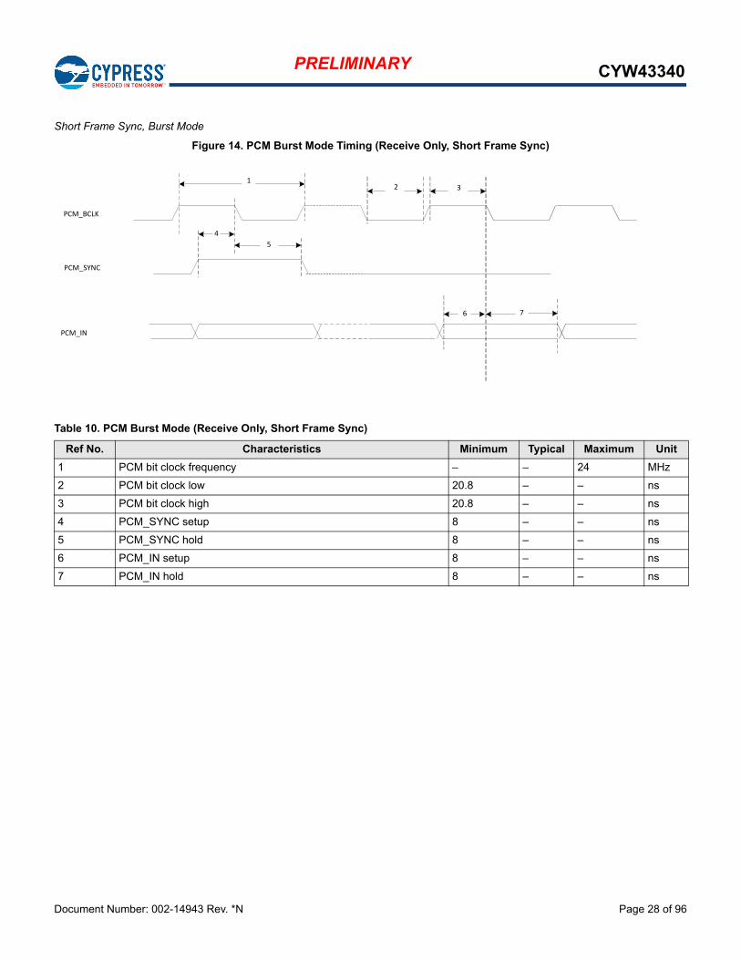
Figure 14. PCM Burst Mode Timing (Receive Only, Short Frame Sync)
Table 10. PCM Burst Mode (Receive Only, Short Frame Sync)
Ref No. Characteristics Minimum Typical Maximum Unit
1 PCM bit clock frequency – – 24 MHz
2 PCM bit clock low 20.8 – – ns
3 PCM bit clock high 20.8 – – ns
4 PCM_SYNC setup 8 – – ns
5 PCM_SYNC hold 8 – – ns
6 PCM_IN setup 8 – – ns
7 PCM_IN hold 8 – – ns
PCM_BCLK
PCM_SYNC
12 3
4
5
PCM_IN
6 7
Document Number: 002-14943 Rev. *N Page 29 of 96
PRELIMINARY CYW43340
Long Frame Sync, Burst Mode
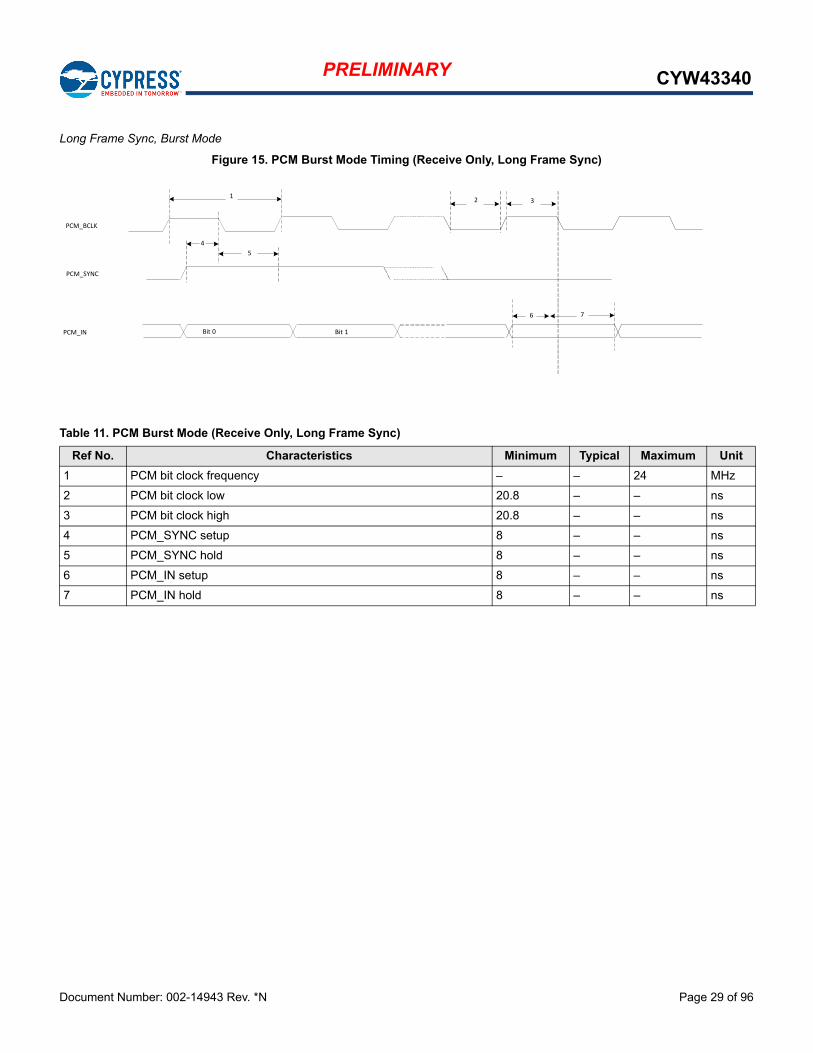
Figure 15. PCM Burst Mode Timing (Receive Only, Long Frame Sync)
Table 11. PCM Burst Mode (Receive Only, Long Frame Sync)
Ref No. Characteristics Minimum Typical Maximum Unit
1 PCM bit clock frequency – – 24 MHz
2 PCM bit clock low 20.8 – – ns
3 PCM bit clock high 20.8 – – ns
4 PCM_SYNC setup 8 – – ns
5 PCM_SYNC hold 8 – – ns
6 PCM_IN setup 8 – – ns
7 PCM_IN hold 8 – – ns
PCM_BCLK
PCM_SYNC
12 3
4
5
PCM_IN
6 7
Bit 0 Bit 1
Document Number: 002-14943 Rev. *N Page 30 of 96
PRELIMINARY CYW43340
7.2 UART Interface
The CYW43340 uses a UART for Bluetooth. The UART is a standard 4-wire interface (RX, TX, RTS, and CTS) with adjustable baudrates from 9600 bps to 4.0 Mbps. The interface features an automatic baud rate detection capability that returns a baud rate selection.Alternatively, the baud rate may be selected through a vendor-specific UART HCI command.
The UART has a 1040-byte receive FIFO and a 1040-byte transmit FIFO to support EDR. Access to the FIFOs is conducted throughthe AHB interface through either DMA or the CPU. The UART supports the Bluetooth 5.0 UART HCI specification: H4 and H5. Thedefault baud rate is 115.2 Kbaud.
The UART supports the 3-wire H5 UART transport, as described in the Bluetooth specification (“Three-wire UART Transport Layer”).Compared to H4, the H5 UART transport reduces the number of signal lines required by eliminating the CTS and RTS signals.
The CYW43340 UART can perform XON/XOFF flow control and includes hardware support for the Serial Line Input Protocol (SLIP).It can also perform wake-on activity. For example, activity on the RX or CTS inputs can wake the chip from a sleep state.
Normally, the UART baud rate is set by a configuration record downloaded after device reset, or by automatic baud rate detection,and the host does not need to adjust the baud rate. Support for changing the baud rate during normal HCI UART operation is includedthrough a vendor-specific command that allows the host to adjust the contents of the baud rate registers. The CYW43340 UARTsoperate correctly with the host UART as long as the combined baud rate error of the two devices is within ±2% (see Table 12).
Table 12. Example of Common Baud Rates
Desired Rate Actual Rate Error (%)
4000000 4000000 0.00
3692000 3692308 0.01
3000000 3000000 0.00
2000000 2000000 0.00
1500000 1500000 0.00
1444444 1454544 0.70
921600 923077 0.16
460800 461538 0.16
230400 230796 0.17
115200 115385 0.16
57600 57692 0.16
38400 38400 0.00
28800 28846 0.16
19200 19200 0.00
14400 14423 0.16
9600 9600 0.00
Document Number: 002-14943 Rev. *N Page 31 of 96
PRELIMINARY CYW43340
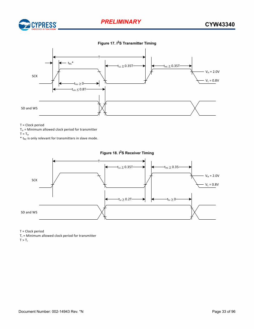
UART timing is defined in Figure 16 and Table 13.
Figure 16. UART Timing
7.3 I2S Interface
The CYW43340 supports an independent I2S digital audio port for high-fidelity Bluetooth audio. The I2S interface supports both masterand slave modes. The I2S signals are:
I2S clock: I2S SCK
I2S Word Select: I2S WS
I2S Data Out: I2S SDO
I2S Data In: I2S SDI
I2S SCK and I2S WS become outputs in master mode and inputs in slave mode, while I2S SDO always stays as an output. The channelword length is 16 bits and the data is justified so that the MSB of the left-channel data is aligned with the MSB of the I2S bus, per theI2S specification. The MSB of each data word is transmitted one bit clock cycle after the I2S WS transition, synchronous with the fallingedge of bit clock. Left-channel data is transmitted when I2S WS is low, and right-channel data is transmitted when I2S WS is high.Data bits sent by the CYW43340 are synchronized with the falling edge of I2S_SCK and should be sampled by the receiver on therising edge of I2S_SSCK.
The clock rate in master mode is either of the following:
48 kHz x 32 bits per frame = 1.536 MHz
48 kHz x 50 bits per frame = 2.400 MHz
The master clock is generated from the input reference clock using a N/M clock divider.
In the slave mode, any clock rate is supported to a maximum of 3.072 MHz.
7.3.1 I2S Timing
Note: Timing values specified in Table 14 are relative to high and low threshold levels.
Table 13. UART Timing Specifications
Ref No. Characteristics Minimum Typical Maximum Unit
1 Delay time, UART_CTS_N low to UART_TXD valid – – 1.5 Bit periods
2 Setup time, UART_CTS_N high before midpoint of stop bit – – 0.5 Bit periods
3 Delay time, midpoint of stop bit to UART_RTS_N high – – 0.5 Bit periods
UART_CTS_N
UART_RXD
UART_RTS_N
1 2
Midpoint of STOP bit
UART_TXD
Midpoint of STOP bit
3
Document Number: 002-14943 Rev. *N Page 32 of 96
PRELIMINARY CYW43340
Note:
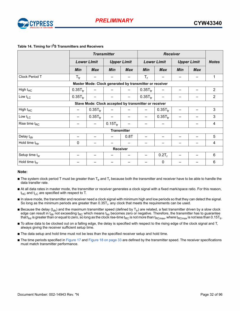
The system clock period T must be greater than Ttr and Tr because both the transmitter and receiver have to be able to handle the data transfer rate.
At all data rates in master mode, the transmitter or receiver generates a clock signal with a fixed mark/space ratio. For this reason, tHC and tLC are specified with respect to T.
In slave mode, the transmitter and receiver need a clock signal with minimum high and low periods so that they can detect the signal. So long as the minimum periods are greater than 0.35Tr, any clock that meets the requirements can be used.
Because the delay (tdtr) and the maximum transmitter speed (defined by Ttr) are related, a fast transmitter driven by a slow clock edge can result in tdtr not exceeding tRC which means thtr becomes zero or negative. Therefore, the transmitter has to guarantee that thtr is greater than or equal to zero, so long as the clock rise-time tRC is not more than tRCmax, where tRCmax is not less than 0.15Ttr.
To allow data to be clocked out on a falling edge, the delay is specified with respect to the rising edge of the clock signal and T, always giving the receiver sufficient setup time.
The data setup and hold time must not be less than the specified receiver setup and hold time.
The time periods specified in Figure 17 and Figure 18 on page 33 are defined by the transmitter speed. The receiver specifications must match transmitter performance.
Table 14. Timing for I2S Transmitters and Receivers
Transmitter Receiver
NotesLower LImit Upper Limit Lower Limit Upper Limit
Min Max Min Max Min Max Min Max
Clock Period T Ttr – – – Tr – – – 1
Master Mode: Clock generated by transmitter or receiver
High tHC 0.35Ttr – – – 0.35Ttr – – – 2
Low tLC 0.35Ttr – – – 0.35Ttr – – – 2
Slave Mode: Clock accepted by transmitter or receiver
High tHC – 0.35Ttr – – – 0.35Ttr – – 3
Low tLC – 0.35Ttr – – – 0.35Ttr – – 3
Rise time tRC – – 0.15Ttr – – – – 4
Transmitter
Delay tdtr – – – 0.8T – – – – 5
Hold time thtr 0 – – – – – – – 4
Receiver
Setup time tsr – – – – – 0.2Tr – – 6
Hold time thr – – – – – 0 – – 6
Document Number: 002-14943 Rev. *N Page 33 of 96
PRELIMINARY CYW43340
Figure 17. I2S Transmitter Timing
Figure 18. I2S Receiver Timing
SD and WS
SCKVL = 0.8V
tLC > 0.35TtRC*
tHC > 0.35T
T
VH = 2.0V
thtr > 0
totr < 0.8T
T = Clock periodTtr = Minimum allowed clock period for transmitterT = Ttr* tRC is only relevant for transmitters in slave mode.
SD and WS
SCKVL = 0.8V
tLC > 0.35T tHC > 0.35
T
VH = 2.0V
thr > 0tsr > 0.2T
T = Clock periodTr = Minimum allowed clock period for transmitterT > Tr
Document Number: 002-14943 Rev. *N Page 34 of 96
PRELIMINARY CYW43340
8. WLAN Global Functions
8.1 WLAN CPU and Memory Subsystem
The CYW43340 includes an integrated ARM Cortex-M3™ processor with internal RAM and ROM. The ARM Cortex-M3 processor isa low-power processor that features low gate count, low interrupt latency, and low-cost debug. It is intended for deeply embeddedapplications that require fast interrupt response features. The processor implements the ARM architecture v7-M with support forThumb®-2 instruction set. ARM Cortex-M3 delivers 30% more performance gain over ARM7TDMI®.
At 0.19 µW/MHz, the Cortex-M3 is the most power efficient general purpose microprocessor available, outperforming 8- and 16-bitdevices on MIPS/µW. It supports integrated sleep modes.
ARM Cortex-M3 uses multiple technologies to reduce cost through improved memory utilization, reduced pin overhead, and reducedsilicon area. ARM Cortex-M3 supports independent buses for code and data access (ICode/DCode and system buses). ARM Cortex-M3 supports extensive debug features including real time trace of program execution.
On-chip memory for the CPU includes 512 KB SRAM and 640 KB ROM.
8.2 One-Time Programmable Memory
Various hardware configuration parameters may be stored in an internal 3072-bit One-Time Programmable (OTP) memory, which isread by the system software after device reset. In addition, customer-specific parameters, including the system vendor ID and theMAC address can be stored, depending on the specific board design.
The initial state of all bits in an unprogrammed OTP device is 0. After any bit is programmed to a 1, it cannot be reprogrammed to 0.The entire OTP array can be programmed in a single write cycle using a utility provided with the Cypress WLAN manufacturing testtools. Alternatively, multiple write cycles can be used to selectively program specific bytes, but only bits which are still in the 0 statecan be altered during each programming cycle.
Prior to OTP programming, all values should be verified using the appropriate editable nvram.txt file, which is provided with thereference board design package.
8.3 GPIO Interface
On the WLBGA package, there are 8 GPIO pins available on the WLAN section of the CYW43340 that can be used to connect tovarious external devices.
Upon power up and reset, these pins become tristated. Subsequently, they can be programmed to be either input or output pins viathe GPIO control register.
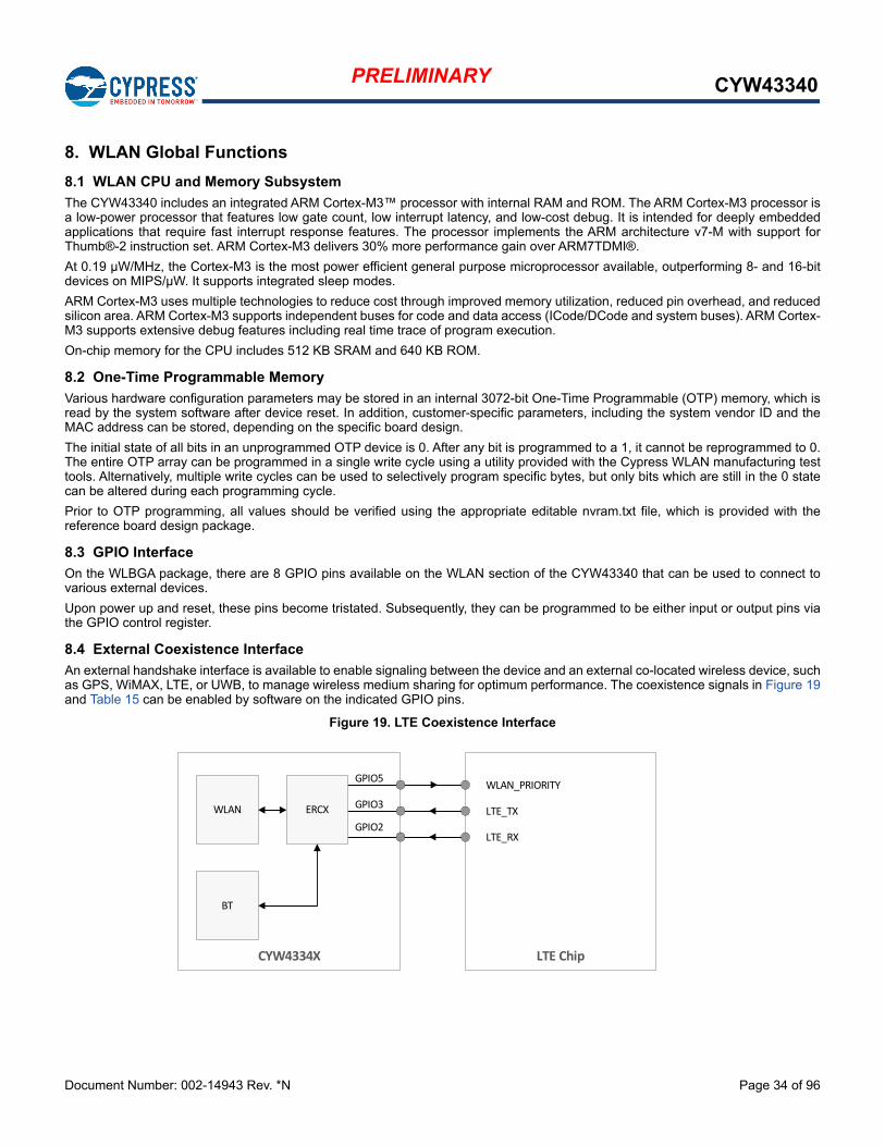
8.4 External Coexistence Interface
An external handshake interface is available to enable signaling between the device and an external co-located wireless device, suchas GPS, WiMAX, LTE, or UWB, to manage wireless medium sharing for optimum performance. The coexistence signals in Figure 19and Table 15 can be enabled by software on the indicated GPIO pins.
Figure 19. LTE Coexistence Interface
CYW4334X
GPIO5
WLAN ERCX GPIO3
GPIO2
LTE Chip
WLAN_PRIORITY
LTE_TX
LTE_RX
BT
Document Number: 002-14943 Rev. *N Page 35 of 96
PRELIMINARY CYW43340
8.5 UART Interface
One UART interface can be enabled by software as an alternate function on pins WL_GPIO4 and WL_GPIO_5. Provided primarilyfor debugging during development, this UART enables the CYW43340 to operate as RS-232 data termination equipment (DTE) forexchanging and managing data with other serial devices. It is compatible with the industry standard 16550 UART and provides a FIFOsize of 64 × 8 in each direction.
8.6 JTAG Interface
The CYW43340 supports the IEEE 1149.1 JTAG boundary scan standard for performing device package and PCB assembly testingduring manufacturing. In addition, the JTAG interface allows Cypress to assist customers by using proprietary debug and character-ization test tools during board bring-up. Therefore, it is highly recommended to provide access to the JTAG pins by means of testpoints or a header on all PCB designs.
Table 15. External Coexistence Interface
Coexistence Signal GPIO Name Type Comment
ERCX_TX_CONF/WLAN_PRIORITY GPIO_5 Output Notify LTE of request to sleep
ERCX_FREQ/LTE_TX GPIO_3 Input Notify WLAN RX of requirement to sleep
ERCX_RF_ACTIVE/LTE_RX GPIO_2 Input Notify WLAN TX to reduce TX power
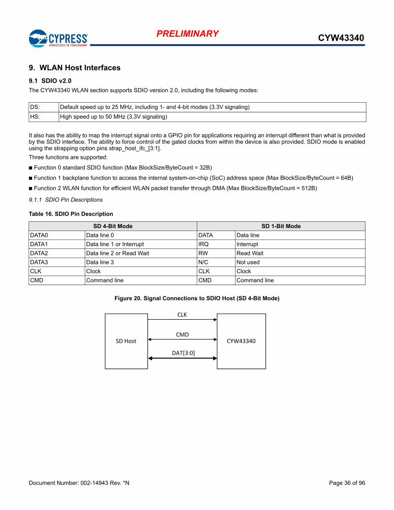
Document Number: 002-14943 Rev. *N Page 36 of 96
PRELIMINARY CYW43340
9. WLAN Host Interfaces
9.1 SDIO v2.0
The CYW43340 WLAN section supports SDIO version 2.0, including the following modes:
It also has the ability to map the interrupt signal onto a GPIO pin for applications requiring an interrupt different than what is providedby the SDIO interface. The ability to force control of the gated clocks from within the device is also provided. SDIO mode is enabledusing the strapping option pins strap_host_ifc_[3:1].
Three functions are supported:
Function 0 standard SDIO function (Max BlockSize/ByteCount = 32B)
Function 1 backplane function to access the internal system-on-chip (SoC) address space (Max BlockSize/ByteCount = 64B)
Function 2 WLAN function for efficient WLAN packet transfer through DMA (Max BlockSize/ByteCount = 512B)
9.1.1 SDIO Pin Descriptions
Figure 20. Signal Connections to SDIO Host (SD 4-Bit Mode)
DS: Default speed up to 25 MHz, including 1- and 4-bit modes (3.3V signaling)
HS: High speed up to 50 MHz (3.3V signaling)
Table 16. SDIO Pin Description
SD 4-Bit Mode SD 1-Bit Mode
DATA0 Data line 0 DATA Data line
DATA1 Data line 1 or Interrupt IRQ Interrupt
DATA2 Data line 2 or Read Wait RW Read Wait
DATA3 Data line 3 N/C Not used
CLK Clock CLK Clock
CMD Command line CMD Command line
SD Host CYW43340
CLK
CMD
DAT[3:0]
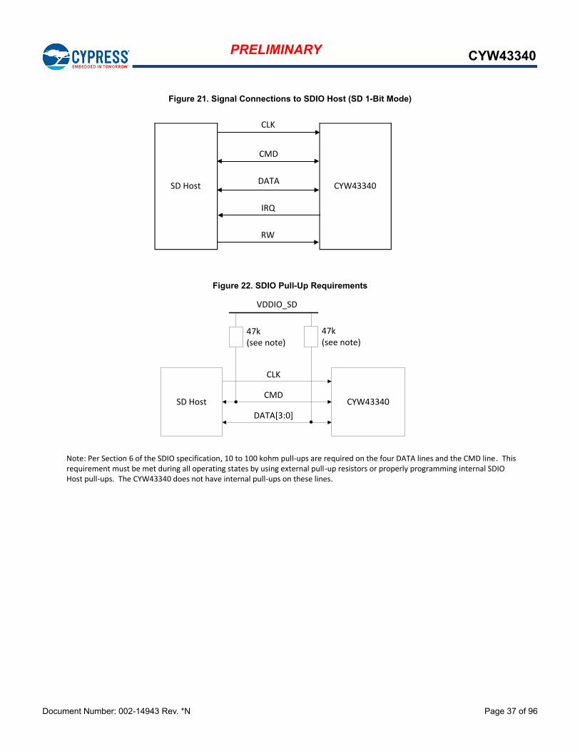
Document Number: 002-14943 Rev. *N Page 37 of 96
PRELIMINARY CYW43340
Figure 21. Signal Connections to SDIO Host (SD 1-Bit Mode)
Figure 22. SDIO Pull-Up Requirements
SD Host CYW43340
CLK
CMD
DATA
IRQ
RW
Note: Per Section 6 of the SDIO specification, 10 to 100 kohm pull-ups are required on the four DATA lines and the CMD line. This requirement must be met during all operating states by using external pull-up resistors or properly programming internal SDIO Host pull-ups. The CYW43340 does not have internal pull-ups on these lines.
SD Host CYW43340
CLK
CMD
DATA[3:0]
VDDIO_SD
47k(see note)
47k(see note)
Document Number: 002-14943 Rev. *N Page 38 of 96
PRELIMINARY CYW43340
9.2 HSIC Interface
As an alternative to SDIO, an HSIC host interface can be enabled using the strapping option pins strap_host_ifc_[3:1]. HSIC is asimplified derivative of the USB2.0 interface designed to replace a standard USB PHY and cable for short distances (up to 10 cm) onboard point-to-point connections. Using two signals, a bidirectional data strobe (STROBE) and a bidirectional DDR data signal (DATA),it provides high-speed serial 480 Mbps data transfers that are 100% host driver compatible with traditional USB 2.0 cable-connectedtopologies.
Figure 23 shows the blocks in the HSIC device core.
Key features of HSIC include:
High-speed 480 Mbps data rate
Source-synchronous serial interface using 1.2V LVCMOS signal levels
No power consumed except when a data transfer is in progress
Maximum trace length of 10 cm.
No Plug-n-Play support, no hot attach/removal
Figure 23. HSIC Device Block Diagram
32-Bit On-Chip Communication System
DMA Engines
RX FIFO TX FIFOs TX FIFOs TX FIFOs TX FIFOs TX FIFOs
TX FIFOs
Endpoint Management Unit
USB 2.0 Protocol Engine
HSIC PHY
Strobe Data
Document Number: 002-14943 Rev. *N Page 39 of 96
PRELIMINARY CYW43340
10. Wireless LAN MAC and PHY
10.1 MAC Features
The CYW43340 WLAN media access controller (MAC) supports features specified in the IEEE 802.11 base standard, and amendedby IEEE 802.11n. The salient features are listed below:
Transmission and reception of aggregated MPDUs (A-MPDU)
Support for power management schemes, including WMM power-save, power-save multi-poll (PSMP) and multiphase PSMP operation
Support for immediate ACK and Block-ACK policies
Interframe space timing support, including RIFS
Support for RTS/CTS and CTS-to-self frame sequences for protecting frame exchanges
Back-off counters in hardware for supporting multiple priorities as specified in the WMM specification
Timing synchronization function (TSF), network allocation vector (NAV) maintenance, and target beacon transmission time (TBTT) generation in hardware
Hardware offload for AES-CCMP, legacy WEP ciphers, WAPI, and support for key management
Support for coexistence with Bluetooth and other external radios
Programmable independent basic service set (IBSS) or infrastructure basic service set functionality
Statistics counters for MIB support
10.1.1 MAC Description
The CYW43340 WLAN MAC is designed to support high-throughput operation with low-power consumption. It does so withoutcompromising the Bluetooth coexistence policies, thereby enabling optimal performance over both networks. In addition, severalpower saving modes have been implemented that allow the MAC to consume very little power while maintaining network-wide timingsynchronization. The architecture diagram of the MAC is shown in Figure 24 on page 40.
The following sections provide an overview of the important modules in the MAC.
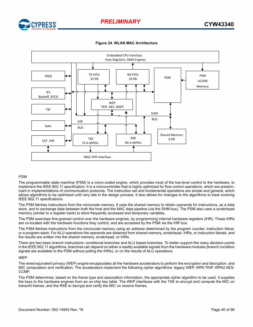
Document Number: 002-14943 Rev. *N Page 40 of 96
PRELIMINARY CYW43340
Figure 24. WLAN MAC Architecture
PSM
The programmable state machine (PSM) is a micro-coded engine, which provides most of the low-level control to the hardware, toimplement the IEEE 802.11 specification. It is a microcontroller that is highly optimized for flow control operations, which are predom-inant in implementations of communication protocols. The instruction set and fundamental operations are simple and general, whichallows algorithms to be optimized until very late in the design process. It also allows for changes to the algorithms to track evolvingIEEE 802.11 specifications.
The PSM fetches instructions from the microcode memory. It uses the shared memory to obtain operands for instructions, as a datastore, and to exchange data between both the host and the MAC data pipeline (via the SHM bus). The PSM also uses a scratchpadmemory (similar to a register bank) to store frequently accessed and temporary variables.
The PSM exercises fine-grained control over the hardware engines, by programming internal hardware registers (IHR). These IHRsare co-located with the hardware functions they control, and are accessed by the PSM via the IHR bus.
The PSM fetches instructions from the microcode memory using an address determined by the program counter, instruction literal,or a program stack. For ALU operations the operands are obtained from shared memory, scratchpad, IHRs, or instruction literals, andthe results are written into the shared memory, scratchpad, or IHRs.
There are two basic branch instructions: conditional branches and ALU based branches. To better support the many decision pointsin the IEEE 802.11 algorithms, branches can depend on either a readily available signals from the hardware modules (branch conditionsignals are available to the PSM without polling the IHRs), or on the results of ALU operations.
WEP
The wired equivalent privacy (WEP) engine encapsulates all the hardware accelerators to perform the encryption and decryption, andMIC computation and verification. The accelerators implement the following cipher algorithms: legacy WEP, WPA TKIP, WPA2 AES-CCMP.
The PSM determines, based on the frame type and association information, the appropriate cipher algorithm to be used. It suppliesthe keys to the hardware engines from an on-chip key table. The WEP interfaces with the TXE to encrypt and compute the MIC ontransmit frames, and the RXE to decrypt and verify the MIC on receive frames.
Embedded CPU InterfaceHost Registers, DMA Engines
TX-FIFO32 KB
WEPTKIP, AES, WAPI
TXETX A-MPDU
RXE
PMQ PSM
Shared Memory6 KB
PSM
UCODE
Memory
EXT- IHR
IFS
Backoff, BTCX
TSF
NAV
IHR
BUS
SHM
BUS
MAC-PHY Interface
RX-FIFO10 KB
RX A-MPDU
Document Number: 002-14943 Rev. *N Page 41 of 96
PRELIMINARY CYW43340
TXE
The transmit engine (TXE) constitutes the transmit data path of the MAC. It coordinates the DMA engines to store the transmit framesin the TXFIFO. It interfaces with WEP module to encrypt frames, and transfers the frames across the MAC-PHY interface at theappropriate time determined by the channel access mechanisms.
The data received from the DMA engines are stored in transmit FIFOs. The MAC supports multiple logical queues to support trafficstreams that have different QoS priority requirements. The PSM uses the channel access information from the IFS module to schedulea queue from which the next frame is transmitted. Once the frame is scheduled, the TXE hardware transmits the frame based on aprecise timing trigger received from the IFS module.
The TXE module also contains the hardware that allows the rapid assembly of MPDUs into an A-MPDU for transmission. The hardwaremodule aggregates the encrypted MPDUs by adding appropriate headers and pad delimiters as needed.
RXE
The receive engine (RXE) constitutes the receive data path of the MAC. It interfaces with the DMA engine to drain the received framesfrom the RXFIFO. It transfers bytes across the MAC-PHY interface and interfaces with the WEP module to decrypt frames. Thedecrypted data is stored in the RXFIFO.
The RXE module contains programmable filters that are programmed by the PSM to accept or filter frames based on several criteriasuch as receiver address, BSSID, and certain frame types.
The RXE module also contains the hardware required to detect A-MPDUs, parse the headers of the containers, and disaggregatethem into component MPDUS.
IFS
The IFS module contains the timers required to determine interframe space timing including RIFS timing. It also contains multiplebackoff engines required to support prioritized access to the medium as specified by WMM.
The interframe spacing timers are triggered by the cessation of channel activity on the medium, as indicated by the PHY. These timersprovide precise timing to the TXE to begin frame transmission. The TXE uses this information to send response frames or performtransmit frame-bursting (RIFS or SIFS separated, as within a TXOP).
The backoff engines (for each access category) monitor channel activity, in each slot duration, to determine whether to continue orpause the backoff counters. When the backoff counters reach 0, the TXE gets notified, so that it may commence frame transmission.In the event of multiple backoff counters decrementing to 0 at the same time, the hardware resolves the conflict based on policiesprovided by the PSM.
The IFS module also incorporates hardware that allows the MAC to enter a low-power state when operating under the IEEE powersave mode. In this mode, the MAC is in a suspended state with its clock turned off. A sleep timer, whose count value is initialized bythe PSM, runs on a slow clock and determines the duration over which the MAC remains in this suspended state. Once the timerexpires the MAC is restored to its functional state. The PSM updates the TSF timer based on the sleep duration ensuring that the TSFis synchronized to the network.
The IFS module also contains the PTA hardware that assists the PSM in Bluetooth coexistence functions.
TSF
The timing synchronization function (TSF) module maintains the TSF timer of the MAC. It also maintains the target beacon trans-mission time (TBTT). The TSF timer hardware, under the control of the PSM, is capable of adopting timestamps received from beaconand probe response frames in order to maintain synchronization with the network.
The TSF module also generates trigger signals for events that are specified as offsets from the TSF timer, such as uplink and downlinktransmission times used in PSMP.
NAV
The network allocation vector (NAV) timer module is responsible for maintaining the NAV information conveyed through the durationfield of MAC frames. This ensures that the MAC complies with the protection mechanisms specified in the standard.
The hardware, under the control of the PSM, maintains the NAV timer and updates the timer appropriately based on received frames.This timing information is provided to the IFS module, which uses it as a virtual carrier-sense indication.
MAC-PHY Interface
The MAC-PHY interface consists of a data path interface to exchange RX/TX data from/to the PHY. In addition, there is anprogramming interface, which can be controlled either by the host or the PSM to configure and control the PHY.
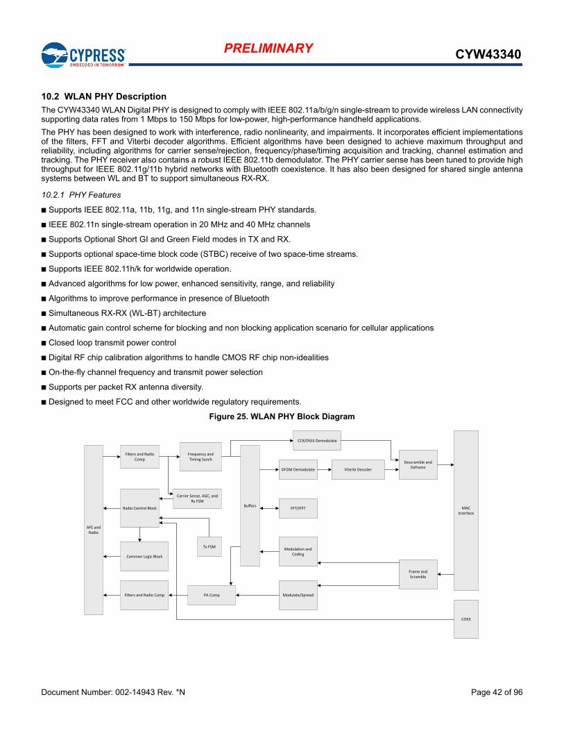
Document Number: 002-14943 Rev. *N Page 42 of 96
PRELIMINARY CYW43340
10.2 WLAN PHY Description
The CYW43340 WLAN Digital PHY is designed to comply with IEEE 802.11a/b/g/n single-stream to provide wireless LAN connectivitysupporting data rates from 1 Mbps to 150 Mbps for low-power, high-performance handheld applications.
The PHY has been designed to work with interference, radio nonlinearity, and impairments. It incorporates efficient implementationsof the filters, FFT and Viterbi decoder algorithms. Efficient algorithms have been designed to achieve maximum throughput andreliability, including algorithms for carrier sense/rejection, frequency/phase/timing acquisition and tracking, channel estimation andtracking. The PHY receiver also contains a robust IEEE 802.11b demodulator. The PHY carrier sense has been tuned to provide highthroughput for IEEE 802.11g/11b hybrid networks with Bluetooth coexistence. It has also been designed for shared single antennasystems between WL and BT to support simultaneous RX-RX.
10.2.1 PHY Features
Supports IEEE 802.11a, 11b, 11g, and 11n single-stream PHY standards.
IEEE 802.11n single-stream operation in 20 MHz and 40 MHz channels
Supports Optional Short GI and Green Field modes in TX and RX.
Supports optional space-time block code (STBC) receive of two space-time streams.
Supports IEEE 802.11h/k for worldwide operation.
Advanced algorithms for low power, enhanced sensitivity, range, and reliability
Algorithms to improve performance in presence of Bluetooth
Simultaneous RX-RX (WL-BT) architecture
Automatic gain control scheme for blocking and non blocking application scenario for cellular applications
Closed loop transmit power control
Digital RF chip calibration algorithms to handle CMOS RF chip non-idealities
On-the-fly channel frequency and transmit power selection
Supports per packet RX antenna diversity.
Designed to meet FCC and other worldwide regulatory requirements.
Figure 25. WLAN PHY Block Diagram
Filters and Radio Comp
Frequency and Timing Synch
Carrier Sense, AGC, and Rx FSM
Radio Control Block
Common Logic Block
Filters and Radio Comp
AFE and Radio
MAC Interface
Buffers
OFDM Demodulate Viterbi Decoder
Tx FSM
PA Comp
Modulation and Coding
Modulate/Spread
Frame and Scramble
FFT/IFFT
CCK/DSSS Demodulate
Descramble and Deframe
COEX
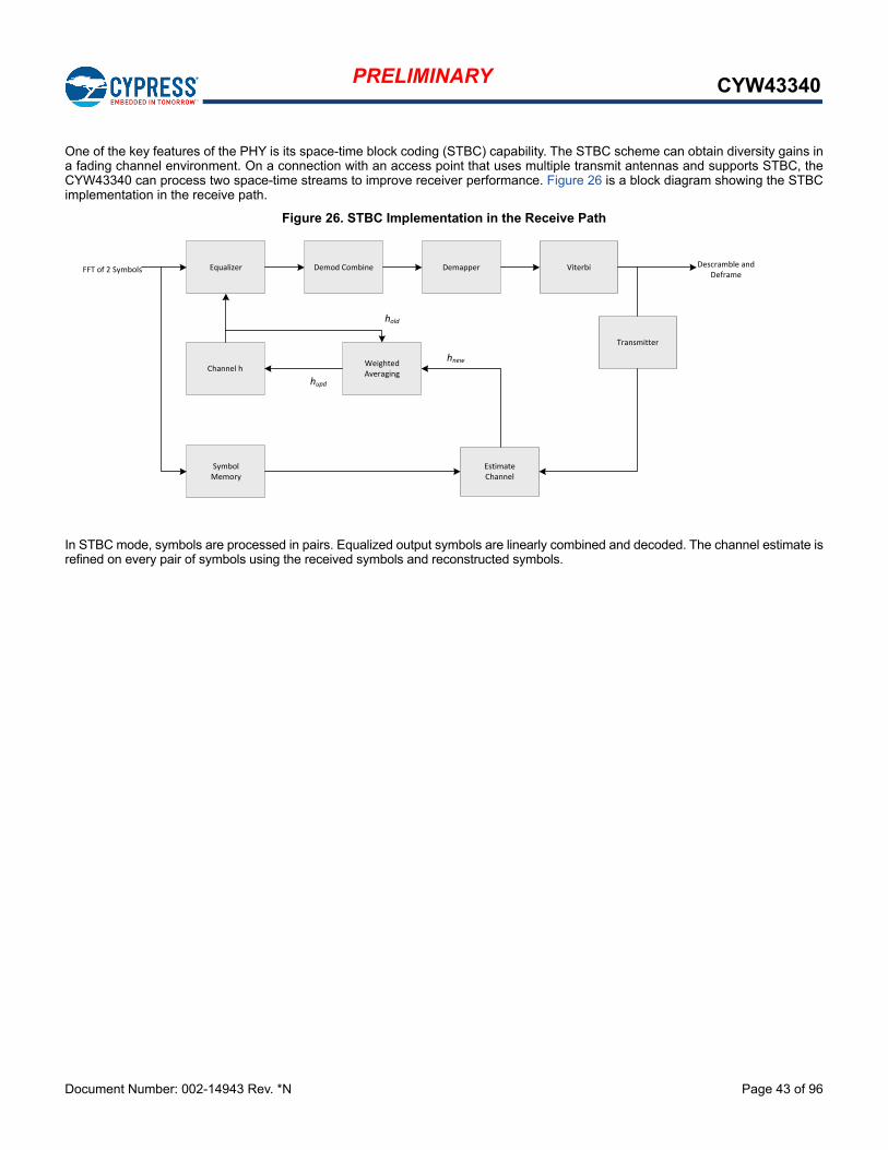
Document Number: 002-14943 Rev. *N Page 43 of 96
PRELIMINARY CYW43340
One of the key features of the PHY is its space-time block coding (STBC) capability. The STBC scheme can obtain diversity gains ina fading channel environment. On a connection with an access point that uses multiple transmit antennas and supports STBC, theCYW43340 can process two space-time streams to improve receiver performance. Figure 26 is a block diagram showing the STBCimplementation in the receive path.
Figure 26. STBC Implementation in the Receive Path
In STBC mode, symbols are processed in pairs. Equalized output symbols are linearly combined and decoded. The channel estimate isrefined on every pair of symbols using the received symbols and reconstructed symbols.
Equalizer Demod Combine Demapper Viterbi
Channel h
SymbolMemory
Weighted Averaging
EstimateChannel
Transmitter
FFT of 2 SymbolsDescramble and
Deframe
hold
hupd
hnew
Document Number: 002-14943 Rev. *N Page 44 of 96
PRELIMINARY CYW43340
11. WLAN Radio Subsystem
The CYW43340 includes an integrated dual-band WLAN RF transceiver that has been optimized for use in 2.4 GHz and 5 GHzWireless LAN systems. It has been designed to provide low-power, low-cost, and robust communications for applications operatingin the globally available 2.4 GHz unlicensed ISM or 5 GHz U-NII bands. The transmit and receive sections include all on-chip filtering,mixing, and gain control functions.
11.1 Receiver Path
The CYW43340 has a wide dynamic range, direct conversion receiver. It employs high order on-chip channel filtering to ensure reliableoperation in the noisy 2.4 GHz ISM band or the entire 5 GHz U-NII band. Control signals are available that can support the use ofoptional external low noise amplifiers (LNA), which can increase the receive sensitivity by several dB.
11.2 Transmit Path
Baseband data is modulated and upconverted to the 2.4 GHz ISM or 5-GHz U-NII bands, respectively. The CYW43340 includes anon-chip regulator which regulates VBAT down to 3.3V for the CYW43340 on-chip linear Power Amplifiers. Closed-loop output powercontrol is provided by means of internal a-band and g-band power detectors.
11.3 Calibration
The CYW43340 features dynamic and automatic on-chip calibration to continually compensate for temperature and process variationsacross components. This enables the CYW43340 to be used in high-volume applications, because calibration routines are notrequired during manufacturing testing. These calibration routines are performed periodically in the course of normal radio operation.Examples of some of the automatic calibration algorithms are baseband filter calibration for optimum transmit and receive performanceand LOFT calibration for carrier leakage reduction. In addition, I/Q Calibration, R Calibration, and VCO Calibration are performed on-chip. No per-board calibration is required in manufacturing test, which helps to minimize test time and cost during large volumeproduction.
Document Number: 002-14943 Rev. *N Page 45 of 96
PRELIMINARY CYW43340
12. Pinout and Signal Descriptions
12.1 Signal AssignmentsFigure 27 shows the WLBGA ball map. Table 17 on page 46 contains the signal description for all packages.
Figure 27. 141-Bump CYW43340 WLBGA Ball Map (Bottom View)
12.2 Signal Descriptions
The signal name, type, and description of each pin in the CYW43340 is listed in Table 17. The symbols shown under Type indicate pin directions (I/O = bidirectional, I = input,O = output) and the internal pull-up/pull-down characteristics (PU = weak internal pull-up resistor and PD = weak internal pull-down resistor), if any. See also Table 18 on page53 for resistor strapping options.
11 10 9 8 7 6 5 4 3 2 1
A FM_LNAVCOVDD FM_RFIN BT_VCOVDD BT_LNAVDD BT_RF BT_PAVDD WRF_RFIN_2G WRF_RFOUT_2G WRF_PAPMU_VOUT_LDO3P3 WRF_RFOUT_5G WRF_PAPMU_VBAT_VDD5P0 A
B FM_VCOVSS FM_LNAVSS BT_VCOVSS BT_PLLVDD BT_PAVSS BT_IFVSS WRF_PA2G_VBAT_VDD3P3 WRF_CBUCK_PAVDD1P5 WRF_PAPMU_GND B
Top layer metal restrict
C FM_AOUT2 FM_PLLVSS BT_IFVDD BT_PLLVSS WRF_PA2G_VBAT_GND3P3 WRF_PA5G_VBAT_GND3P3_C3 WRF_PA5G_VBAT_GND3P3_C2 WRF_RFIN_5G C
Depopulated
D FM_AOUT1 FM_PLLVDD BT_I2S_WS BT_I2S_CLK VSSC_D6 WRF_LNA_2G_GND1P2 WRF_PADRV_VBAT_VDD3P3 WRF_PADRV_VBAT_GND3P3 WRF_GPIO_OUT WRF_LNA_5G_GND1P2 D
E CLK_REQ BT_DEV_WAKE VDDC_E9 BT_PCM_OUT BT_I2S_DO WRF_RX_GND1P2 WRF_TX_GND1P2 WRF_VCO_GND1P2 E
F LPO_IN BT_HOST_WAKE BT_PCM_IN BT_PCM_CLK BT_PCM_SYNC WRF_AFE_GND1P2 WRF_BUCK_VDD1P5 WL_GPIO_1 WRF_SYNTH_VDD1P2 WRF_XTAL_CAB_VDD1P2 F
G BT_UART_CTS_N BT_UART_TXD NC_G9 RF_SW_CTRL_3 VSSC_G7 RF_SW_CTRL_2 WL_GPIO_6 WL_GPIO_2 WL_GPIO_0 WRF_SYNTH_GND1P2 WRF_XTAL_CAB_XOP G
H BT_UART_RTS_N BT_UART_RXD VDDIO_H9 RF_SW_CTRL_4 VDDC_H7 RF_SW_CTRL_1 WL_GPIO_5 WL_GPIO_3 WRF_TCXO_VDD1P8 WRF_XTAL_CAB_GND1P2 WRF_XTAL_CAB_XON H
J NC_J11 VSS_J10 NC_J9 VSS_J8 WL_GPIO_4 VDDIO_RF WL_GPIO_12 VDDIO_J4 WRF_TCXO_CKIN2V BT_REG_ON WL_REG_ON J
K VSS_K11 VSS_K10 NC_K9 VSS_K8 NC_K7 SDIO_DATA_2 SDIO_DATA_3 RREFHSIC HSIC_DATA VDDC_K1 K
L VSS_L11 VSS_L10 VSS_L9 VSS_L8 NC_L7 RF_SW_CTRL_0 SDIO_DATA_0 SDIO_DATA_1 HSIC_DVDD1P2_OUT HSIC_STROBE HSIC_AGND12PLL L
M VSS_M11 VSS_M10 VSS_M9 VSS_M8 NC_M7 SDIO_CLK SDIO_CMD JTAG_SEL VSSC_M2 PMU_AVSS M
N VSS_N11 VSS_N10 VSS_N9 VSS_N8 VSS_N7 VSSC_N6 VOUT_2P5 VOUT_CLDO SR_VDDBATA5V SR_VLX N
P VSS_P11 VSS_P10 VSS_P9 VSS_P8 VSS_P7 VSS_P6 VDDC_P5 VOUT_LNLDO LDO_VDD1P5 SR_VDDBATP5V SR_PVSS P
11 10 9 8 7 6 5 4 3 2 1
Document Number: 002-14943 Rev. *N Page 46 of 96
PRELIMINARY CYW43340
Table 17. WLBGA Signal Descriptions
WLBGA Ball Signal Name Type Description
WLAN RF Signal Interface
A5 WRF_RFIN_2G I 2.4G RF input
C1 WRF_RFIN_5G I 5G RF input
A4 WRF_RFOUT_2G O 2.4G RF output
A2 WRF_RFOUT_5G O 5G RF output
D2 WRF_GPIO_OUT I/O –
RF Control Signals
L6 RF_SW_CTRL_0 O RF switch enable
H6 RF_SW_CTRL_1 O RF switch enable
G6 RF_SW_CTRL_2 O RF switch enable
G8 RF_SW_CTRL_3 O RF switch enable
H8 RF_SW_CTRL_4 O RF switch enable
SDIO Bus Interface
M6 SDIO_CLK I SDIO clock input
M5 SDIO_CMD I/O SDIO command line
L5 SDIO_DATA_0 I/O SDIO data line 0
L4 SDIO_DATA_1 I/O SDIO data line 1. Also used as a strapping option (see Table 18 on page 53).
K5 SDIO_DATA_2 I/O SDIO data line 2. Also used as a strapping option (see Table 18 on page 53).
K4 SDIO_DATA_3 I/O SDIO data line 3
Note: Per Section 6 of the SDIO specification, 10 to 100 kohm pull-ups are required on the four DATA lines and the CMDline. This requirement must be met during all operating states by using external pull-up resistors or properlyprogramming internal SDIO Host pull-ups.
JTAG Interface
M4 JTAG_SEL I/O JTAG select: Connect this pin high (VDDIO) in order to use GPIO_2 through GPIO_5 and GPIO_12 as JTAG signals. Otherwise, if this pin is left as a NO_CONNECT, its internal pull-down selects the default mode that allows GPIOs 2, 3, 4, 5, and 12 to be used as GPIOs.
Note: See “WLAN GPIO Interface” onpage 47 for the JTAG signal pins.
HSIC Interface
L2 HSIC_STROBE I HSIC Strobe
K2 HSIC_DATA I/O HSIC Data
K3 RREFHSIC I HSIC reference resistor input. If HSIC is used, connect this pin to ground via a 51Ω 5% resistor.
Document Number: 002-14943 Rev. *N Page 47 of 96
PRELIMINARY CYW43340
WLAN GPIO Interface
G3 WL_GPIO_0 I/O This pin can be programmed by software to be a GPIO.
F3 WL_GPIO_1 I/O This pin can be programmed by software to be a GPIO or an AP_READY or HSIC_HOST_READY input from the host indicating that it is awake.
G4 WL_GPIO_2 I/O This pin can be programmed by software to be a GPIO, the JTAG TCK or an HSIC_READY output to the host, indicating that the device is ready to respond with a CONNECT when it sees IDLE on the HSIC bus.
H4 WL_GPIO_3 I/O This pin can be programmed by software to be a GPIO or the JTAG TMS signal.
J7 WL_GPIO_4 I/O This pin can be programmed by software to be a GPIO, the JTAG TDI signal, the UART RX signal, or as theWLAN_HOST_WAKE output indicatingthat host wake-up should be performed.
H5 WL_GPIO_5 I/O This pin can be programmed by software to be a GPIO, the JTAG TDO signal or the UART TX signal.
G5 WL_GPIO_6 I/O GPIO pin.
Note: Some GPIOs are also used as strapping options (see Table 18 on page 53).
J5 WL_GPIO_12 I/O This pin can be programmed by software to be a GPIO or the JTAG TRST_L signal. GPIO12 has an internal pull-down by default if JTAG_SEL is low. When JTAG_SEL is high, GPIO12 is used as JTAG_TRST_L and is pulled up. This pin is also used as WLAN_DEV_WAKE, an out-of- band wake-up signal when the host wants to wake WLAN from the deep sleep mode.
Note: Some GPIOs are also used as strapping options (see Table 18 on page 53).
Table 17. WLBGA Signal Descriptions (Cont.)
WLBGA Ball Signal Name Type Description
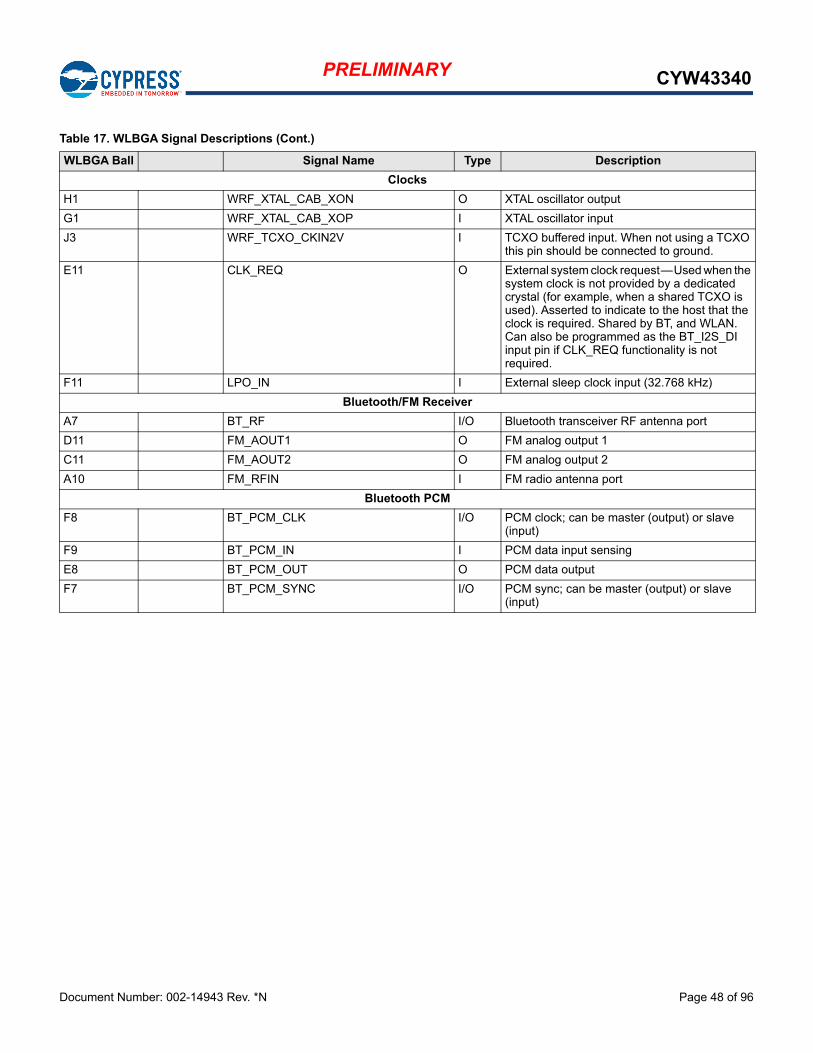
Document Number: 002-14943 Rev. *N Page 48 of 96
PRELIMINARY CYW43340
Clocks
H1 WRF_XTAL_CAB_XON O XTAL oscillator output
G1 WRF_XTAL_CAB_XOP I XTAL oscillator input
J3 WRF_TCXO_CKIN2V I TCXO buffered input. When not using a TCXO this pin should be connected to ground.
E11 CLK_REQ O External system clock request—Used when the system clock is not provided by a dedicated crystal (for example, when a shared TCXO is used). Asserted to indicate to the host that the clock is required. Shared by BT, and WLAN. Can also be programmed as the BT_I2S_DI input pin if CLK_REQ functionality is not required.
F11 LPO_IN I External sleep clock input (32.768 kHz)
Bluetooth/FM Receiver
A7 BT_RF I/O Bluetooth transceiver RF antenna port
D11 FM_AOUT1 O FM analog output 1
C11 FM_AOUT2 O FM analog output 2
A10 FM_RFIN I FM radio antenna port
Bluetooth PCM
F8 BT_PCM_CLK I/O PCM clock; can be master (output) or slave (input)
F9 BT_PCM_IN I PCM data input sensing
E8 BT_PCM_OUT O PCM data output
F7 BT_PCM_SYNC I/O PCM sync; can be master (output) or slave (input)
Table 17. WLBGA Signal Descriptions (Cont.)
WLBGA Ball Signal Name Type Description
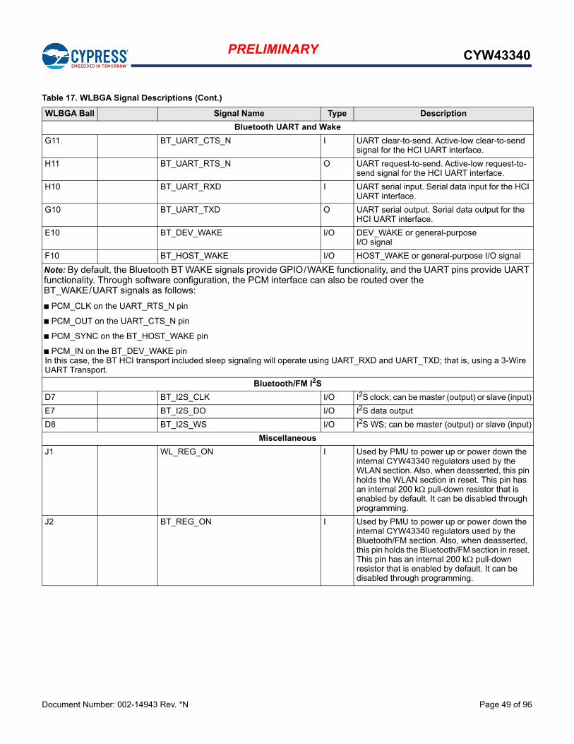
Document Number: 002-14943 Rev. *N Page 49 of 96
PRELIMINARY CYW43340
Bluetooth UART and Wake
G11 BT_UART_CTS_N I UART clear-to-send. Active-low clear-to-send signal for the HCI UART interface.
H11 BT_UART_RTS_N O UART request-to-send. Active-low request-to-send signal for the HCI UART interface.
H10 BT_UART_RXD I UART serial input. Serial data input for the HCI UART interface.
G10 BT_UART_TXD O UART serial output. Serial data output for the HCI UART interface.
E10 BT_DEV_WAKE I/O DEV_WAKE or general-purpose I/O signal
F10 BT_HOST_WAKE I/O HOST_WAKE or general-purpose I/O signal
Note: By default, the Bluetooth BT WAKE signals provide GPIO/WAKE functionality, and the UART pins provide UART functionality. Through software configuration, the PCM interface can also be routed over the BT_WAKE/UART signals as follows:
PCM_CLK on the UART_RTS_N pin
PCM_OUT on the UART_CTS_N pin
PCM_SYNC on the BT_HOST_WAKE pin
PCM_IN on the BT_DEV_WAKE pinIn this case, the BT HCI transport included sleep signaling will operate using UART_RXD and UART_TXD; that is, using a 3-Wire UART Transport.
Bluetooth/FM I2S
D7 BT_I2S_CLK I/O I2S clock; can be master (output) or slave (input)
E7 BT_I2S_DO I/O I2S data output
D8 BT_I2S_WS I/O I2S WS; can be master (output) or slave (input)
Miscellaneous
J1 WL_REG_ON I Used by PMU to power up or power down the internal CYW43340 regulators used by the WLAN section. Also, when deasserted, this pin holds the WLAN section in reset. This pin has an internal 200 k pull-down resistor that is enabled by default. It can be disabled through programming.
J2 BT_REG_ON I Used by PMU to power up or power down the internal CYW43340 regulators used by the Bluetooth/FM section. Also, when deasserted, this pin holds the Bluetooth/FM section in reset. This pin has an internal 200 k pull-down resistor that is enabled by default. It can be disabled through programming.
Table 17. WLBGA Signal Descriptions (Cont.)
WLBGA Ball Signal Name Type Description
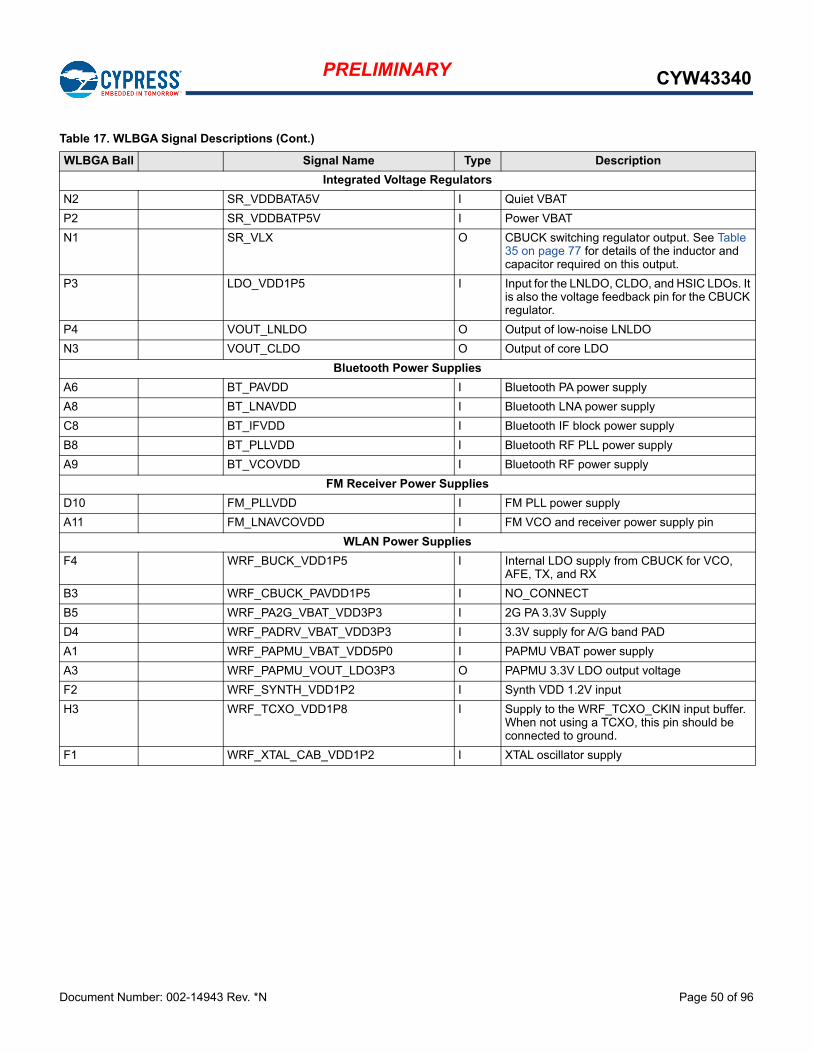
Document Number: 002-14943 Rev. *N Page 50 of 96
PRELIMINARY CYW43340
Integrated Voltage Regulators
N2 SR_VDDBATA5V I Quiet VBAT
P2 SR_VDDBATP5V I Power VBAT
N1 SR_VLX O CBUCK switching regulator output. See Table 35 on page 77 for details of the inductor and capacitor required on this output.
P3 LDO_VDD1P5 I Input for the LNLDO, CLDO, and HSIC LDOs. It is also the voltage feedback pin for the CBUCK regulator.
P4 VOUT_LNLDO O Output of low-noise LNLDO
N3 VOUT_CLDO O Output of core LDO
Bluetooth Power Supplies
A6 BT_PAVDD I Bluetooth PA power supply
A8 BT_LNAVDD I Bluetooth LNA power supply
C8 BT_IFVDD I Bluetooth IF block power supply
B8 BT_PLLVDD I Bluetooth RF PLL power supply
A9 BT_VCOVDD I Bluetooth RF power supply
FM Receiver Power Supplies
D10 FM_PLLVDD I FM PLL power supply
A11 FM_LNAVCOVDD I FM VCO and receiver power supply pin
WLAN Power Supplies
F4 WRF_BUCK_VDD1P5 I Internal LDO supply from CBUCK for VCO, AFE, TX, and RX
B3 WRF_CBUCK_PAVDD1P5 I NO_CONNECT
B5 WRF_PA2G_VBAT_VDD3P3 I 2G PA 3.3V Supply
D4 WRF_PADRV_VBAT_VDD3P3 I 3.3V supply for A/G band PAD
A1 WRF_PAPMU_VBAT_VDD5P0 I PAPMU VBAT power supply
A3 WRF_PAPMU_VOUT_LDO3P3 O PAPMU 3.3V LDO output voltage
F2 WRF_SYNTH_VDD1P2 I Synth VDD 1.2V input
H3 WRF_TCXO_VDD1P8 I Supply to the WRF_TCXO_CKIN input buffer. When not using a TCXO, this pin should be connected to ground.
F1 WRF_XTAL_CAB_VDD1P2 I XTAL oscillator supply
Table 17. WLBGA Signal Descriptions (Cont.)
WLBGA Ball Signal Name Type Description
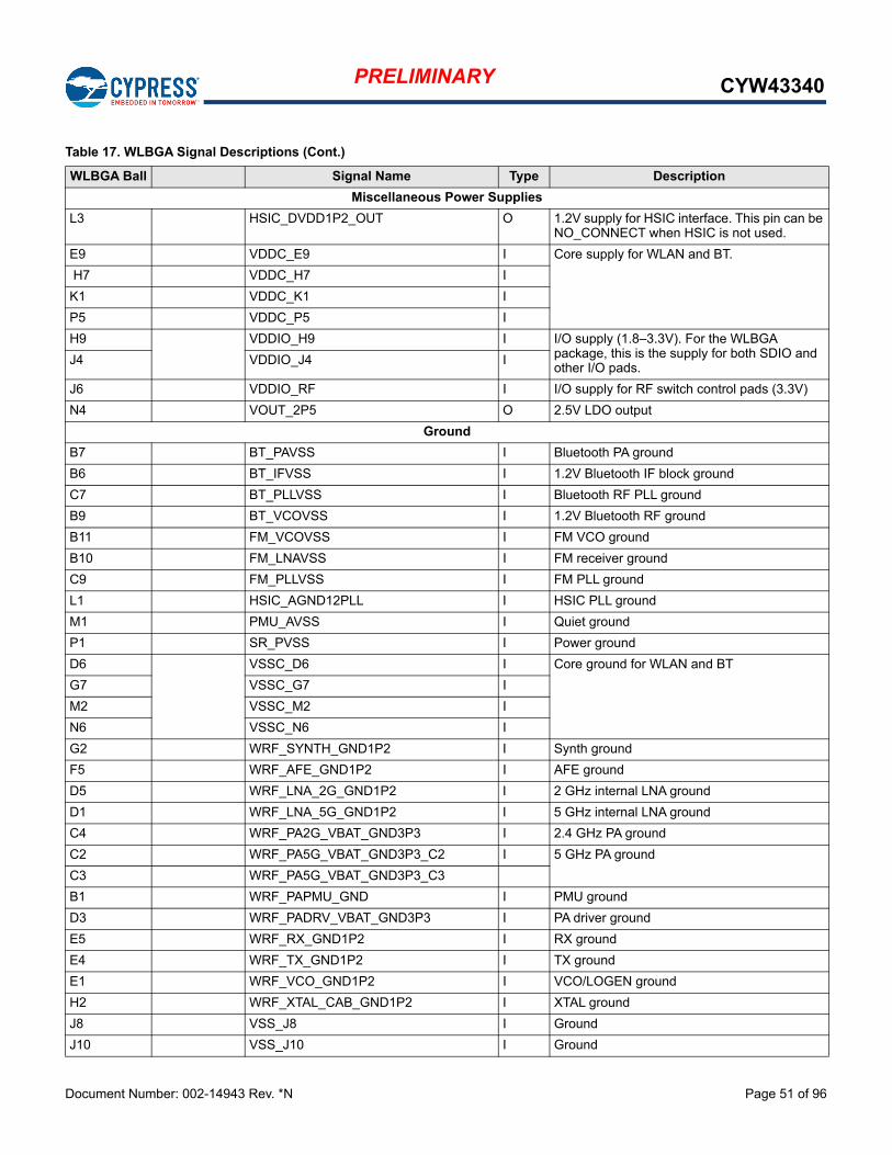
Document Number: 002-14943 Rev. *N Page 51 of 96
PRELIMINARY CYW43340
Miscellaneous Power Supplies
L3 HSIC_DVDD1P2_OUT O 1.2V supply for HSIC interface. This pin can be NO_CONNECT when HSIC is not used.
E9 VDDC_E9 I Core supply for WLAN and BT.
H7 VDDC_H7 I
K1 VDDC_K1 I
P5 VDDC_P5 I
H9 VDDIO_H9 I I/O supply (1.8–3.3V). For the WLBGA package, this is the supply for both SDIO and other I/O pads.
J4 VDDIO_J4 I
J6 VDDIO_RF I I/O supply for RF switch control pads (3.3V)
N4 VOUT_2P5 O 2.5V LDO output
Ground
B7 BT_PAVSS I Bluetooth PA ground
B6 BT_IFVSS I 1.2V Bluetooth IF block ground
C7 BT_PLLVSS I Bluetooth RF PLL ground
B9 BT_VCOVSS I 1.2V Bluetooth RF ground
B11 FM_VCOVSS I FM VCO ground
B10 FM_LNAVSS I FM receiver ground
C9 FM_PLLVSS I FM PLL ground
L1 HSIC_AGND12PLL I HSIC PLL ground
M1 PMU_AVSS I Quiet ground
P1 SR_PVSS I Power ground
D6 VSSC_D6 I Core ground for WLAN and BT
G7 VSSC_G7 I
M2 VSSC_M2 I
N6 VSSC_N6 I
G2 WRF_SYNTH_GND1P2 I Synth ground
F5 WRF_AFE_GND1P2 I AFE ground
D5 WRF_LNA_2G_GND1P2 I 2 GHz internal LNA ground
D1 WRF_LNA_5G_GND1P2 I 5 GHz internal LNA ground
C4 WRF_PA2G_VBAT_GND3P3 I 2.4 GHz PA ground
C2 WRF_PA5G_VBAT_GND3P3_C2 I 5 GHz PA ground
C3 WRF_PA5G_VBAT_GND3P3_C3
B1 WRF_PAPMU_GND I PMU ground
D3 WRF_PADRV_VBAT_GND3P3 I PA driver ground
E5 WRF_RX_GND1P2 I RX ground
E4 WRF_TX_GND1P2 I TX ground
E1 WRF_VCO_GND1P2 I VCO/LOGEN ground
H2 WRF_XTAL_CAB_GND1P2 I XTAL ground
J8 VSS_J8 I Ground
J10 VSS_J10 I Ground
Table 17. WLBGA Signal Descriptions (Cont.)
WLBGA Ball Signal Name Type Description
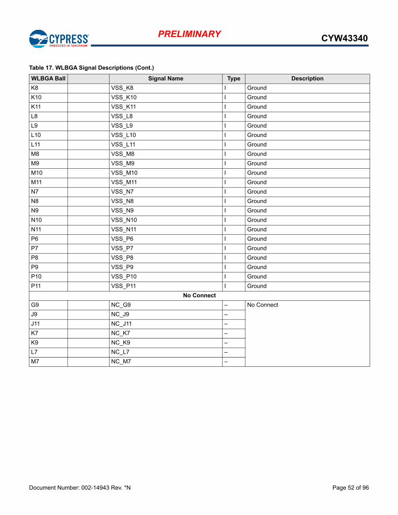
Document Number: 002-14943 Rev. *N Page 52 of 96
PRELIMINARY CYW43340
K8 VSS_K8 I Ground
K10 VSS_K10 I Ground
K11 VSS_K11 I Ground
L8 VSS_L8 I Ground
L9 VSS_L9 I Ground
L10 VSS_L10 I Ground
L11 VSS_L11 I Ground
M8 VSS_M8 I Ground
M9 VSS_M9 I Ground
M10 VSS_M10 I Ground
M11 VSS_M11 I Ground
N7 VSS_N7 I Ground
N8 VSS_N8 I Ground
N9 VSS_N9 I Ground
N10 VSS_N10 I Ground
N11 VSS_N11 I Ground
P6 VSS_P6 I Ground
P7 VSS_P7 I Ground
P8 VSS_P8 I Ground
P9 VSS_P9 I Ground
P10 VSS_P10 I Ground
P11 VSS_P11 I Ground
No Connect
G9 NC_G9 – No Connect
J9 NC_J9 –
J11 NC_J11 –
K7 NC_K7 –
K9 NC_K9 –
L7 NC_L7 –
M7 NC_M7 –
Table 17. WLBGA Signal Descriptions (Cont.)
WLBGA Ball Signal Name Type Description
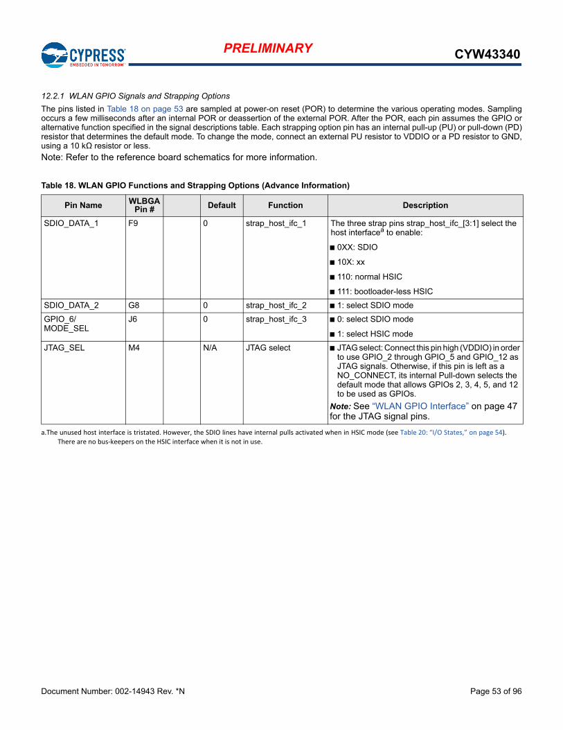
Document Number: 002-14943 Rev. *N Page 53 of 96
PRELIMINARY CYW43340
12.2.1 WLAN GPIO Signals and Strapping Options
The pins listed in Table 18 on page 53 are sampled at power-on reset (POR) to determine the various operating modes. Samplingoccurs a few milliseconds after an internal POR or deassertion of the external POR. After the POR, each pin assumes the GPIO oralternative function specified in the signal descriptions table. Each strapping option pin has an internal pull-up (PU) or pull-down (PD)resistor that determines the default mode. To change the mode, connect an external PU resistor to VDDIO or a PD resistor to GND,using a 10 kΩ resistor or less.
Note: Refer to the reference board schematics for more information.
Table 18. WLAN GPIO Functions and Strapping Options (Advance Information)
Pin Name WLBGA Pin # Default Function Description
SDIO_DATA_1 F9 0 strap_host_ifc_1 The three strap pins strap_host_ifc_[3:1] select the host interfacea to enable:
0XX: SDIO
10X: xx
110: normal HSIC
111: bootloader-less HSIC
a.The unused host interface is tristated. However, the SDIO lines have internal pulls activated when in HSIC mode (see Table 20: “I/O States,” on page 54).
There are no bus-keepers on the HSIC interface when it is not in use.
SDIO_DATA_2 G8 0 strap_host_ifc_2 1: select SDIO mode
GPIO_6/MODE_SEL
J6 0 strap_host_ifc_3 0: select SDIO mode
1: select HSIC mode
JTAG_SEL M4 N/A JTAG select JTAG select: Connect this pin high (VDDIO) in order to use GPIO_2 through GPIO_5 and GPIO_12 as JTAG signals. Otherwise, if this pin is left as a NO_CONNECT, its internal Pull-down selects the default mode that allows GPIOs 2, 3, 4, 5, and 12 to be used as GPIOs.
Note: See “WLAN GPIO Interface” on page 47 for the JTAG signal pins.
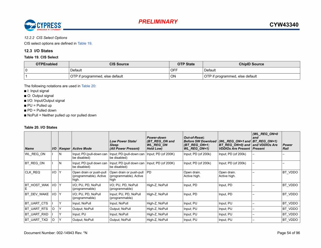
Document Number: 002-14943 Rev. *N Page 54 of 96
PRELIMINARY CYW43340
12.2.2 CIS Select Options
CIS select options are defined in Table 19.
12.3 I/O States
The following notations are used in Table 20: I: Input signal O: Output signal I/O: Input/Output signal PU = Pulled up PD = Pulled down NoPull = Neither pulled up nor pulled down
Table 19. CIS Select
OTPEnabled CIS Source OTP State ChipID Source
0 Default OFF Default
1 OTP if programmed, else default ON OTP if programmed, else default
Table 20. I/O States
Name I/O Keeper Active Mode
Low Power State/Sleep (All Power Present)
Power-down (BT_REG_ON and WL_REG_ONHeld Low)
Out-of-Reset; Before SW Download (BT_REG_ON=1; WL_REG_ON=1)
(WL_REG_ON=1 and BT_REG_ON=0) and VDDIOs Are Present
(WL_REG_ON=0 and BT_REG_ON=1) and VDDIOs Are Present
Power Rail
WL_REG_ON I N Input; PD (pull-down can be disabled)
Input; PD (pull-down can be disabled)
Input; PD (of 200K) Input; PD (of 200k) Input; PD (of 200k) – –
BT_REG_ON I N Input; PD (pull down can be disabled)
Input; PD (pull down can be disabled)
Input; PD (of 200K) Input; PD (of 200k) Input; PD (of 200k) – –
CLK_REQ I/O Y Open drain or push-pull (programmable). Active high.
Open drain or push-pull (programmable). Active high
PD Open drain. Active high.
Open drain. Active high.
– BT_VDDO
BT_HOST_WAKE
I/O Y I/O; PU, PD, NoPull (programmable)
I/O; PU, PD, NoPull (programmable)
High-Z, NoPull Input, PD Input, PD – BT_VDDO
BT_DEV_WAKE I/O Y I/O; PU, PD, NoPull (programmable)
Input; PU, PD, NoPull (programmable)
High-Z, NoPull Input, PD Input, PD – BT_VDDO
BT_UART_CTS I Y Input; NoPull Input; NoPull High-Z, NoPull Input; PU Input; PU – BT_VDDO
BT_UART_RTS O Y Output; NoPull Output; NoPull High-Z, NoPull Input; PU Input; PU – BT_VDDO
BT_UART_RXD I Y Input; PU Input; NoPull High-Z, NoPull Input; PU Input; PU – BT_VDDO
BT_UART_TXD O Y Output; NoPull Output; NoPull High-Z, NoPull Input; PU Input; PU – BT_VDDO
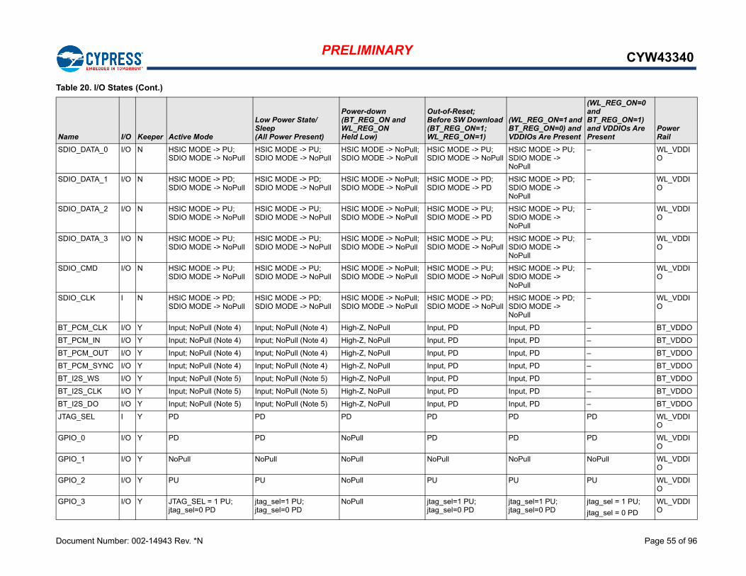
Document Number: 002-14943 Rev. *N Page 55 of 96
PRELIMINARY CYW43340
SDIO_DATA_0 I/O N HSIC MODE -> PU; SDIO MODE -> NoPull
HSIC MODE -> PU; SDIO MODE -> NoPull
HSIC MODE -> NoPull; SDIO MODE -> NoPull
HSIC MODE -> PU; SDIO MODE -> NoPull
HSIC MODE -> PU; SDIO MODE -> NoPull
– WL_VDDIO
SDIO_DATA_1 I/O N HSIC MODE -> PD; SDIO MODE -> NoPull
HSIC MODE -> PD; SDIO MODE -> NoPull
HSIC MODE -> NoPull; SDIO MODE -> NoPull
HSIC MODE -> PD; SDIO MODE -> PD
HSIC MODE -> PD; SDIO MODE -> NoPull
– WL_VDDIO
SDIO_DATA_2 I/O N HSIC MODE -> PU; SDIO MODE -> NoPull
HSIC MODE -> PU; SDIO MODE -> NoPull
HSIC MODE -> NoPull; SDIO MODE -> NoPull
HSIC MODE -> PU; SDIO MODE -> PD
HSIC MODE -> PU; SDIO MODE -> NoPull
– WL_VDDIO
SDIO_DATA_3 I/O N HSIC MODE -> PU; SDIO MODE -> NoPull
HSIC MODE -> PU; SDIO MODE -> NoPull
HSIC MODE -> NoPull; SDIO MODE -> NoPull
HSIC MODE -> PU; SDIO MODE -> NoPull
HSIC MODE -> PU; SDIO MODE -> NoPull
– WL_VDDIO
SDIO_CMD I/O N HSIC MODE -> PU; SDIO MODE -> NoPull
HSIC MODE -> PU; SDIO MODE -> NoPull
HSIC MODE -> NoPull; SDIO MODE -> NoPull
HSIC MODE -> PU; SDIO MODE -> NoPull
HSIC MODE -> PU; SDIO MODE -> NoPull
– WL_VDDIO
SDIO_CLK I N HSIC MODE -> PD; SDIO MODE -> NoPull
HSIC MODE -> PD;SDIO MODE -> NoPull
HSIC MODE -> NoPull; SDIO MODE -> NoPull
HSIC MODE -> PD; SDIO MODE -> NoPull
HSIC MODE -> PD; SDIO MODE -> NoPull
– WL_VDDIO
BT_PCM_CLK I/O Y Input; NoPull (Note 4) Input; NoPull (Note 4) High-Z, NoPull Input, PD Input, PD – BT_VDDO
BT_PCM_IN I/O Y Input; NoPull (Note 4) Input; NoPull (Note 4) High-Z, NoPull Input, PD Input, PD – BT_VDDO
BT_PCM_OUT I/O Y Input; NoPull (Note 4) Input; NoPull (Note 4) High-Z, NoPull Input, PD Input, PD – BT_VDDO
BT_PCM_SYNC I/O Y Input; NoPull (Note 4) Input; NoPull (Note 4) High-Z, NoPull Input, PD Input, PD – BT_VDDO
BT_I2S_WS I/O Y Input; NoPull (Note 5) Input; NoPull (Note 5) High-Z, NoPull Input, PD Input, PD – BT_VDDO
BT_I2S_CLK I/O Y Input; NoPull (Note 5) Input; NoPull (Note 5) High-Z, NoPull Input, PD Input, PD – BT_VDDO
BT_I2S_DO I/O Y Input; NoPull (Note 5) Input; NoPull (Note 5) High-Z, NoPull Input, PD Input, PD – BT_VDDO
JTAG_SEL I Y PD PD PD PD PD PD WL_VDDIO
GPIO_0 I/O Y PD PD NoPull PD PD PD WL_VDDIO
GPIO_1 I/O Y NoPull NoPull NoPull NoPull NoPull NoPull WL_VDDIO
GPIO_2 I/O Y PU PU NoPull PU PU PU WL_VDDIO
GPIO_3 I/O Y JTAG_SEL = 1 PU; jtag_sel=0 PD
jtag_sel=1 PU; jtag_sel=0 PD
NoPull jtag_sel=1 PU; jtag_sel=0 PD
jtag_sel=1 PU; jtag_sel=0 PD
jtag_sel = 1 PU;
jtag_sel = 0 PD
WL_VDDIO
Table 20. I/O States (Cont.)
Name I/O Keeper Active Mode
Low Power State/Sleep (All Power Present)
Power-down (BT_REG_ON and WL_REG_ONHeld Low)
Out-of-Reset; Before SW Download (BT_REG_ON=1; WL_REG_ON=1)
(WL_REG_ON=1 and BT_REG_ON=0) and VDDIOs Are Present
(WL_REG_ON=0 and BT_REG_ON=1) and VDDIOs Are Present
Power Rail
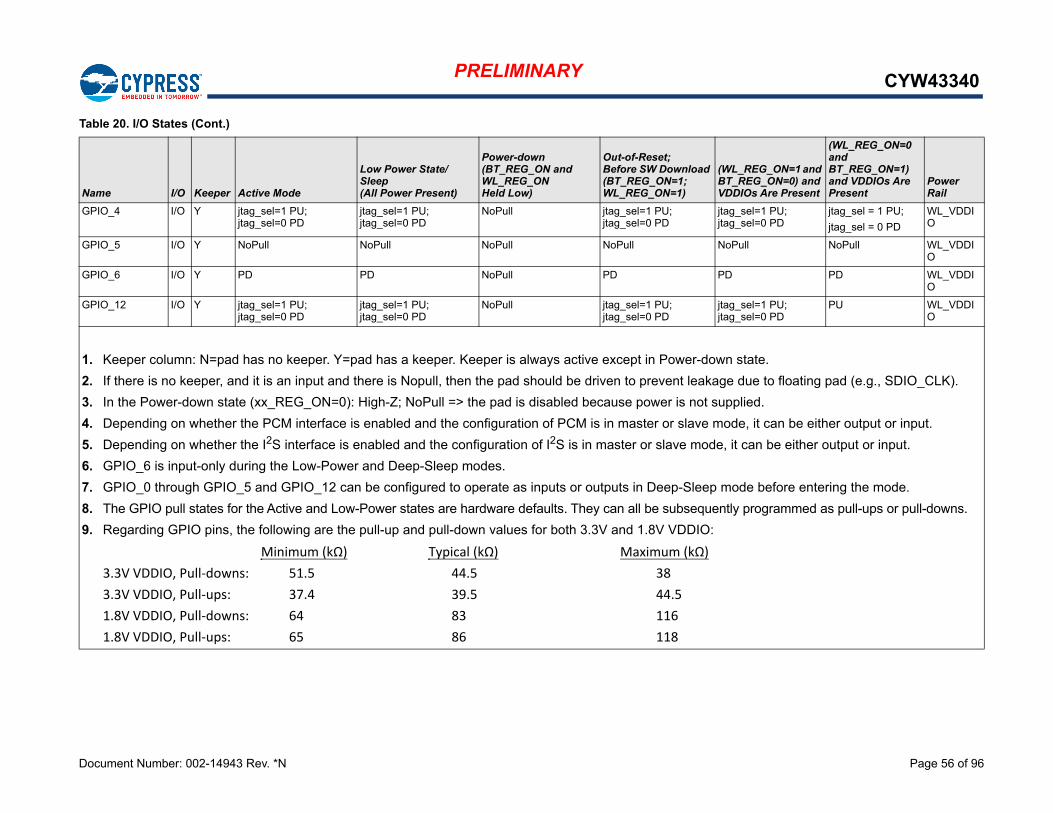
Document Number: 002-14943 Rev. *N Page 56 of 96
PRELIMINARY CYW43340
GPIO_4 I/O Y jtag_sel=1 PU; jtag_sel=0 PD
jtag_sel=1 PU; jtag_sel=0 PD
NoPull jtag_sel=1 PU; jtag_sel=0 PD
jtag_sel=1 PU; jtag_sel=0 PD
jtag_sel = 1 PU;
jtag_sel = 0 PD
WL_VDDIO
GPIO_5 I/O Y NoPull NoPull NoPull NoPull NoPull NoPull WL_VDDIO
GPIO_6 I/O Y PD PD NoPull PD PD PD WL_VDDIO
GPIO_12 I/O Y jtag_sel=1 PU; jtag_sel=0 PD
jtag_sel=1 PU; jtag_sel=0 PD
NoPull jtag_sel=1 PU; jtag_sel=0 PD
jtag_sel=1 PU; jtag_sel=0 PD
PU WL_VDDIO
1. Keeper column: N=pad has no keeper. Y=pad has a keeper. Keeper is always active except in Power-down state.
2. If there is no keeper, and it is an input and there is Nopull, then the pad should be driven to prevent leakage due to floating pad (e.g., SDIO_CLK).
3. In the Power-down state (xx_REG_ON=0): High-Z; NoPull => the pad is disabled because power is not supplied.
4. Depending on whether the PCM interface is enabled and the configuration of PCM is in master or slave mode, it can be either output or input.
5. Depending on whether the I2S interface is enabled and the configuration of I2S is in master or slave mode, it can be either output or input.
6. GPIO_6 is input-only during the Low-Power and Deep-Sleep modes.
7. GPIO_0 through GPIO_5 and GPIO_12 can be configured to operate as inputs or outputs in Deep-Sleep mode before entering the mode.
8. The GPIO pull states for the Active and Low-Power states are hardware defaults. They can all be subsequently programmed as pull-ups or pull-downs.
9. Regarding GPIO pins, the following are the pull-up and pull-down values for both 3.3V and 1.8V VDDIO:
Minimum (kΩ) Typical (kΩ) Maximum (kΩ)
3.3V VDDIO, Pull-downs: 51.5 44.5 38
3.3V VDDIO, Pull-ups: 37.4 39.5 44.5
1.8V VDDIO, Pull-downs: 64 83 116
1.8V VDDIO, Pull-ups: 65 86 118
Table 20. I/O States (Cont.)
Name I/O Keeper Active Mode
Low Power State/Sleep (All Power Present)
Power-down (BT_REG_ON and WL_REG_ONHeld Low)
Out-of-Reset; Before SW Download (BT_REG_ON=1; WL_REG_ON=1)
(WL_REG_ON=1 and BT_REG_ON=0) and VDDIOs Are Present
(WL_REG_ON=0 and BT_REG_ON=1) and VDDIOs Are Present
Power Rail
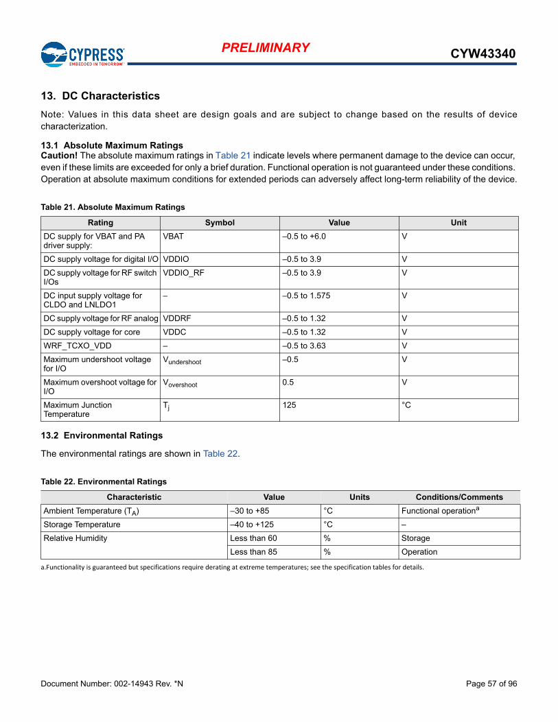
Document Number: 002-14943 Rev. *N Page 57 of 96
PRELIMINARY CYW43340
13. DC Characteristics
Note: Values in this data sheet are design goals and are subject to change based on the results of devicecharacterization.
13.1 Absolute Maximum RatingsCaution! The absolute maximum ratings in Table 21 indicate levels where permanent damage to the device can occur, even if these limits are exceeded for only a brief duration. Functional operation is not guaranteed under these conditions. Operation at absolute maximum conditions for extended periods can adversely affect long-term reliability of the device.
13.2 Environmental Ratings
The environmental ratings are shown in Table 22.
Table 21. Absolute Maximum Ratings
Rating Symbol Value Unit
DC supply for VBAT and PA driver supply:
VBAT –0.5 to +6.0 V
DC supply voltage for digital I/O VDDIO –0.5 to 3.9 V
DC supply voltage for RF switch I/Os
VDDIO_RF –0.5 to 3.9 V
DC input supply voltage for CLDO and LNLDO1
– –0.5 to 1.575 V
DC supply voltage for RF analog VDDRF –0.5 to 1.32 V
DC supply voltage for core VDDC –0.5 to 1.32 V
WRF_TCXO_VDD – –0.5 to 3.63 V
Maximum undershoot voltage for I/O
Vundershoot –0.5 V
Maximum overshoot voltage for I/O
Vovershoot 0.5 V
Maximum Junction Temperature
Tj 125 °C
Table 22. Environmental Ratings
Characteristic Value Units Conditions/Comments
Ambient Temperature (TA) –30 to +85 °C Functional operationa
a.Functionality is guaranteed but specifications require derating at extreme temperatures; see the specification tables for details.
Storage Temperature –40 to +125 °C –
Relative Humidity Less than 60 % Storage
Less than 85 % Operation
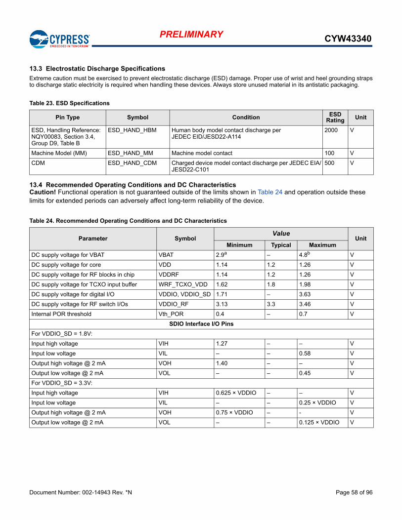
Document Number: 002-14943 Rev. *N Page 58 of 96
PRELIMINARY CYW43340
13.3 Electrostatic Discharge Specifications
Extreme caution must be exercised to prevent electrostatic discharge (ESD) damage. Proper use of wrist and heel grounding strapsto discharge static electricity is required when handling these devices. Always store unused material in its antistatic packaging.
13.4 Recommended Operating Conditions and DC CharacteristicsCaution! Functional operation is not guaranteed outside of the limits shown in Table 24 and operation outside these limits for extended periods can adversely affect long-term reliability of the device.
Table 23. ESD Specifications
Pin Type Symbol Condition ESD Rating Unit
ESD, Handling Reference: NQY00083, Section 3.4, Group D9, Table B
ESD_HAND_HBM Human body model contact discharge perJEDEC EID/JESD22-A114
2000 V
Machine Model (MM) ESD_HAND_MM Machine model contact 100 V
CDM ESD_HAND_CDM Charged device model contact discharge per JEDEC EIA/JESD22-C101
500 V
Table 24. Recommended Operating Conditions and DC Characteristics
Parameter SymbolValue
UnitMinimum Typical Maximum
DC supply voltage for VBAT VBAT 2.9a – 4.8b V
DC supply voltage for core VDD 1.14 1.2 1.26 V
DC supply voltage for RF blocks in chip VDDRF 1.14 1.2 1.26 V
DC supply voltage for TCXO input buffer WRF_TCXO_VDD 1.62 1.8 1.98 V
DC supply voltage for digital I/O VDDIO, VDDIO_SD 1.71 – 3.63 V
DC supply voltage for RF switch I/Os VDDIO_RF 3.13 3.3 3.46 V
Internal POR threshold Vth_POR 0.4 – 0.7 V
SDIO Interface I/O Pins
For VDDIO_SD = 1.8V:
Input high voltage VIH 1.27 – – V
Input low voltage VIL – – 0.58 V
Output high voltage @ 2 mA VOH 1.40 – – V
Output low voltage @ 2 mA VOL – – 0.45 V
For VDDIO_SD = 3.3V:
Input high voltage VIH 0.625 × VDDIO – – V
Input low voltage VIL – – 0.25 × VDDIO V
Output high voltage @ 2 mA VOH 0.75 × VDDIO – - V
Output low voltage @ 2 mA VOL – – 0.125 × VDDIO V
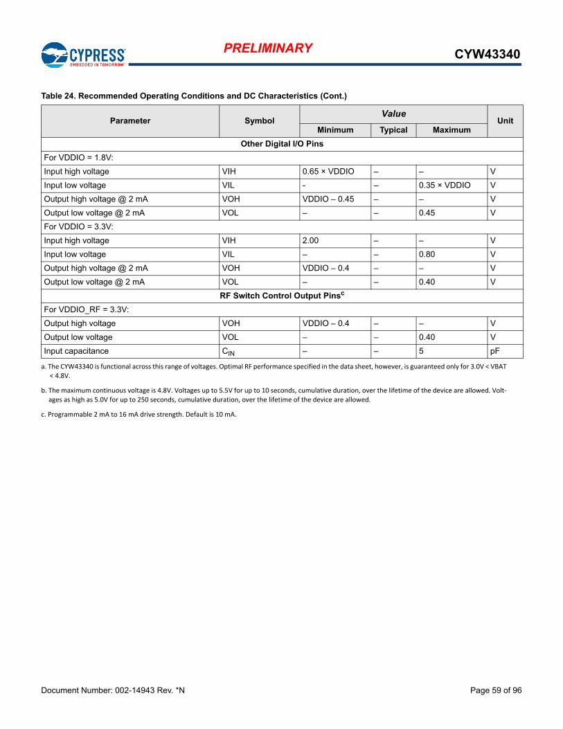
Document Number: 002-14943 Rev. *N Page 59 of 96
PRELIMINARY CYW43340
Other Digital I/O Pins
For VDDIO = 1.8V:
Input high voltage VIH 0.65 × VDDIO – – V
Input low voltage VIL - – 0.35 × VDDIO V
Output high voltage @ 2 mA VOH VDDIO – 0.45 – – V
Output low voltage @ 2 mA VOL – – 0.45 V
For VDDIO = 3.3V:
Input high voltage VIH 2.00 – – V
Input low voltage VIL – – 0.80 V
Output high voltage @ 2 mA VOH VDDIO – 0.4 – – V
Output low voltage @ 2 mA VOL – – 0.40 V
RF Switch Control Output Pinsc
For VDDIO_RF = 3.3V:
Output high voltage VOH VDDIO – 0.4 – – V
Output low voltage VOL – – 0.40 V
Input capacitance CIN – – 5 pF
a. The CYW43340 is functional across this range of voltages. Optimal RF performance specified in the data sheet, however, is guaranteed only for 3.0V < VBAT
< 4.8V.
b. The maximum continuous voltage is 4.8V. Voltages up to 5.5V for up to 10 seconds, cumulative duration, over the lifetime of the device are allowed. Volt-
ages as high as 5.0V for up to 250 seconds, cumulative duration, over the lifetime of the device are allowed.
c. Programmable 2 mA to 16 mA drive strength. Default is 10 mA.
Table 24. Recommended Operating Conditions and DC Characteristics (Cont.)
Parameter SymbolValue
UnitMinimum Typical Maximum
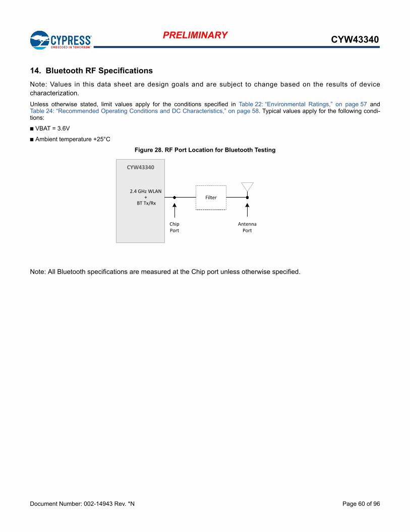
Document Number: 002-14943 Rev. *N Page 60 of 96
PRELIMINARY CYW43340
14. Bluetooth RF Specifications
Note: Values in this data sheet are design goals and are subject to change based on the results of devicecharacterization.
Unless otherwise stated, limit values apply for the conditions specified in Table 22: “Environmental Ratings,” on page 57 andTable 24: “Recommended Operating Conditions and DC Characteristics,” on page 58. Typical values apply for the following condi-tions:
VBAT = 3.6V
Ambient temperature +25°C
Figure 28. RF Port Location for Bluetooth Testing
Note: All Bluetooth specifications are measured at the Chip port unless otherwise specified.
CYW43340
Antenna Port
2.4 GHz WLAN+
BT Tx/Rx
ChipPort
Filter
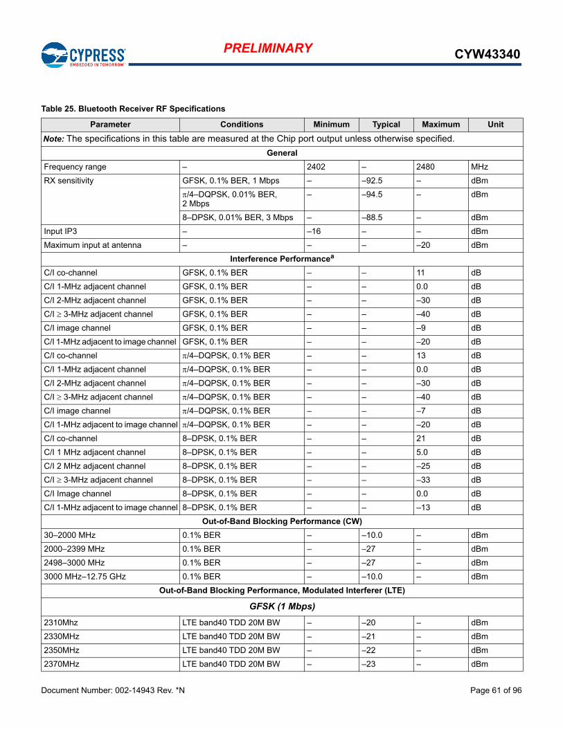
Document Number: 002-14943 Rev. *N Page 61 of 96
PRELIMINARY CYW43340
Table 25. Bluetooth Receiver RF Specifications
Parameter Conditions Minimum Typical Maximum Unit
Note: The specifications in this table are measured at the Chip port output unless otherwise specified.
General
Frequency range – 2402 – 2480 MHz
RX sensitivity GFSK, 0.1% BER, 1 Mbps – –92.5 – dBm
/4–DQPSK, 0.01% BER, 2 Mbps
– –94.5 – dBm
8–DPSK, 0.01% BER, 3 Mbps – –88.5 – dBm
Input IP3 – –16 – – dBm
Maximum input at antenna – – – –20 dBm
Interference Performancea
C/I co-channel GFSK, 0.1% BER – – 11 dB
C/I 1-MHz adjacent channel GFSK, 0.1% BER – – 0.0 dB
C/I 2-MHz adjacent channel GFSK, 0.1% BER – – –30 dB
C/I 3-MHz adjacent channel GFSK, 0.1% BER – – –40 dB
C/I image channel GFSK, 0.1% BER – – –9 dB
C/I 1-MHz adjacent to image channel GFSK, 0.1% BER – – –20 dB
C/I co-channel /4–DQPSK, 0.1% BER – – 13 dB
C/I 1-MHz adjacent channel /4–DQPSK, 0.1% BER – – 0.0 dB
C/I 2-MHz adjacent channel /4–DQPSK, 0.1% BER – – –30 dB
C/I 3-MHz adjacent channel /4–DQPSK, 0.1% BER – – –40 dB
C/I image channel /4–DQPSK, 0.1% BER – – –7 dB
C/I 1-MHz adjacent to image channel /4–DQPSK, 0.1% BER – – –20 dB
C/I co-channel 8–DPSK, 0.1% BER – – 21 dB
C/I 1 MHz adjacent channel 8–DPSK, 0.1% BER – – 5.0 dB
C/I 2 MHz adjacent channel 8–DPSK, 0.1% BER – – –25 dB
C/I 3-MHz adjacent channel 8–DPSK, 0.1% BER – – –33 dB
C/I Image channel 8–DPSK, 0.1% BER – – 0.0 dB
C/I 1-MHz adjacent to image channel 8–DPSK, 0.1% BER – – –13 dB
Out-of-Band Blocking Performance (CW)
30–2000 MHz 0.1% BER – –10.0 – dBm
2000–2399 MHz 0.1% BER – –27 – dBm
2498–3000 MHz 0.1% BER – –27 – dBm
3000 MHz–12.75 GHz 0.1% BER – –10.0 – dBm
Out-of-Band Blocking Performance, Modulated Interferer (LTE)
GFSK (1 Mbps)
2310Mhz LTE band40 TDD 20M BW – –20 – dBm
2330MHz LTE band40 TDD 20M BW – –21 – dBm
2350MHz LTE band40 TDD 20M BW – –22 – dBm
2370MHz LTE band40 TDD 20M BW – –23 – dBm
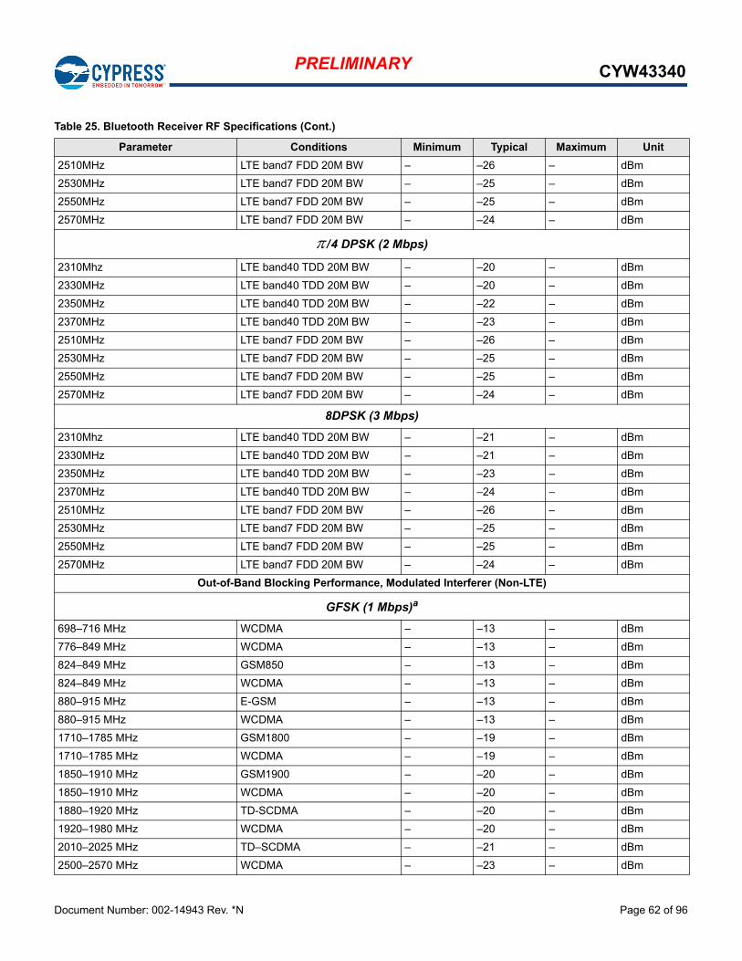
Document Number: 002-14943 Rev. *N Page 62 of 96
PRELIMINARY CYW43340
2510MHz LTE band7 FDD 20M BW – –26 – dBm
2530MHz LTE band7 FDD 20M BW – –25 – dBm
2550MHz LTE band7 FDD 20M BW – –25 – dBm
2570MHz LTE band7 FDD 20M BW – –24 – dBm
/4 DPSK (2 Mbps)
2310Mhz LTE band40 TDD 20M BW – –20 – dBm
2330MHz LTE band40 TDD 20M BW – –20 – dBm
2350MHz LTE band40 TDD 20M BW – –22 – dBm
2370MHz LTE band40 TDD 20M BW – –23 – dBm
2510MHz LTE band7 FDD 20M BW – –26 – dBm
2530MHz LTE band7 FDD 20M BW – –25 – dBm
2550MHz LTE band7 FDD 20M BW – –25 – dBm
2570MHz LTE band7 FDD 20M BW – –24 – dBm
8DPSK (3 Mbps)
2310Mhz LTE band40 TDD 20M BW – –21 – dBm
2330MHz LTE band40 TDD 20M BW – –21 – dBm
2350MHz LTE band40 TDD 20M BW – –23 – dBm
2370MHz LTE band40 TDD 20M BW – –24 – dBm
2510MHz LTE band7 FDD 20M BW – –26 – dBm
2530MHz LTE band7 FDD 20M BW – –25 – dBm
2550MHz LTE band7 FDD 20M BW – –25 – dBm
2570MHz LTE band7 FDD 20M BW – –24 – dBm
Out-of-Band Blocking Performance, Modulated Interferer (Non-LTE)
GFSK (1 Mbps)a
698–716 MHz WCDMA – –13 – dBm
776–849 MHz WCDMA – –13 – dBm
824–849 MHz GSM850 – –13 – dBm
824–849 MHz WCDMA – –13 – dBm
880–915 MHz E-GSM – –13 – dBm
880–915 MHz WCDMA – –13 – dBm
1710–1785 MHz GSM1800 – –19 – dBm
1710–1785 MHz WCDMA – –19 – dBm
1850–1910 MHz GSM1900 – –20 – dBm
1850–1910 MHz WCDMA – –20 – dBm
1880–1920 MHz TD-SCDMA – –20 – dBm
1920–1980 MHz WCDMA – –20 – dBm
2010–2025 MHz TD–SCDMA – –21 – dBm
2500–2570 MHz WCDMA – –23 – dBm
Table 25. Bluetooth Receiver RF Specifications (Cont.)
Parameter Conditions Minimum Typical Maximum Unit
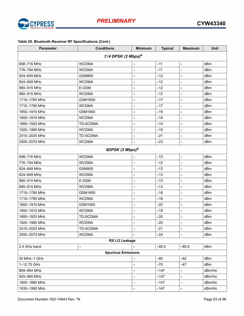
Document Number: 002-14943 Rev. *N Page 63 of 96
PRELIMINARY CYW43340
/4 DPSK (2 Mbps)a
698–716 MHz WCDMA – –11 – dBm
776–794 MHz WCDMA – –11 – dBm
824–849 MHz GSM850 – –12 – dBm
824–849 MHz WCDMA – –12 – dBm
880–915 MHz E-GSM – –12 – dBm
880–915 MHz WCDMA – –12 – dBm
1710–1785 MHz GSM1800 – –17 – dBm
1710–1785 MHz WCDMA – –17 – dBm
1850–1910 MHz GSM1900 – –19 – dBm
1850–1910 MHz WCDMA – –18 – dBm
1880–1920 MHz TD-SCDMA – –19 – dBm
1920–1980 MHz WCDMA – –19 – dBm
2010–2025 MHz TD-SCDMA – –21 – dBm
2500–2570 MHz WCDMA – –23 – dBm
8DPSK (3 Mbps)a
698–716 MHz WCDMA – –13 – dBm
776–794 MHz WCDMA – –12 – dBm
824–849 MHz GSM850 – –13 – dBm
824–849 MHz WCDMA – –13 – dBm
880–915 MHz E-GSM – –13 – dBm
880–915 MHz WCDMA – –13 – dBm
1710–1785 MHz GSM1800 – –18 – dBm
1710–1785 MHz WCDMA – –18 – dBm
1850–1910 MHz GSM1900 – –20 – dBm
1850–1910 MHz WCDMA – –19 – dBm
1880–1920 MHz TD-SCDMA – –20 – dBm
1920–1980 MHz WCDMA – –20 – dBm
2010–2025 MHz TD-SCDMA – –21 – dBm
2500–2570 MHz WCDMA – –24 – dBm
RX LO Leakage
2.4 GHz band – – –90.0 –80.0 dBm
Spurious Emissions
30 MHz–1 GHz – –95 –62 dBm
1–12.75 GHz – –70 –47 dBm
869–894 MHz – –147 – dBm/Hz
925–960 MHz – –147 – dBm/Hz
1805–1880 MHz – –147 – dBm/Hz
1930–1990 MHz – –147 – dBm/Hz
Table 25. Bluetooth Receiver RF Specifications (Cont.)
Parameter Conditions Minimum Typical Maximum Unit
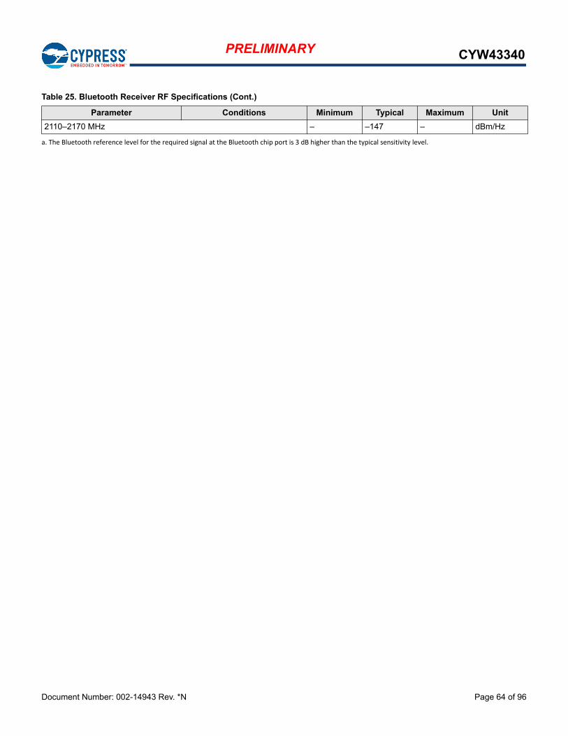
Document Number: 002-14943 Rev. *N Page 64 of 96
PRELIMINARY CYW43340
2110–2170 MHz – –147 – dBm/Hz
a. The Bluetooth reference level for the required signal at the Bluetooth chip port is 3 dB higher than the typical sensitivity level.
Table 25. Bluetooth Receiver RF Specifications (Cont.)
Parameter Conditions Minimum Typical Maximum Unit
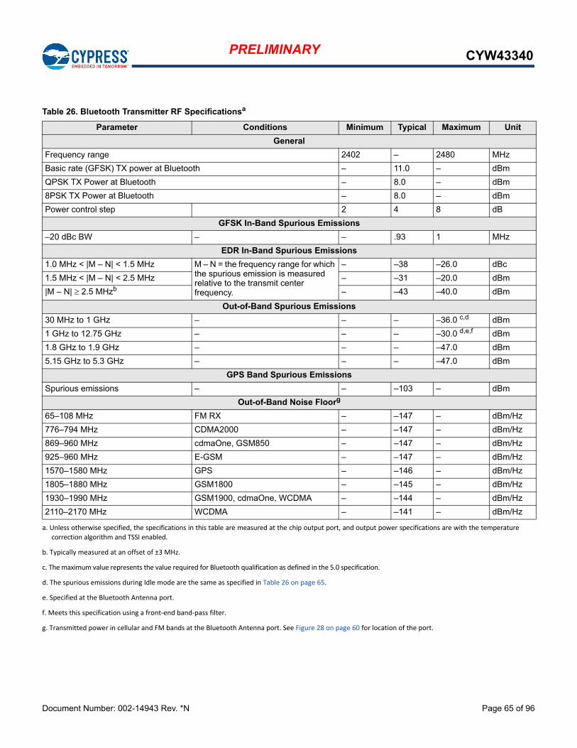
Document Number: 002-14943 Rev. *N Page 65 of 96
PRELIMINARY CYW43340
Table 26. Bluetooth Transmitter RF Specificationsa
a. Unless otherwise specified, the specifications in this table are measured at the chip output port, and output power specifications are with the temperature
correction algorithm and TSSI enabled.
Parameter Conditions Minimum Typical Maximum Unit
General
Frequency range 2402 – 2480 MHz
Basic rate (GFSK) TX power at Bluetooth – 11.0 – dBm
QPSK TX Power at Bluetooth – 8.0 – dBm
8PSK TX Power at Bluetooth – 8.0 – dBm
Power control step 2 4 8 dB
GFSK In-Band Spurious Emissions
–20 dBc BW – – .93 1 MHz
EDR In-Band Spurious Emissions
1.0 MHz < |M – N| < 1.5 MHz M – N = the frequency range for which the spurious emission is measured relative to the transmit center frequency.
– –38 –26.0 dBc
1.5 MHz < |M – N| < 2.5 MHz – –31 –20.0 dBm
|M – N| 2.5 MHzb
b. Typically measured at an offset of ±3 MHz.
– –43 –40.0 dBm
Out-of-Band Spurious Emissions
30 MHz to 1 GHz – – – –36.0 c,d
c. The maximum value represents the value required for Bluetooth qualification as defined in the 5.0 specification.
d. The spurious emissions during Idle mode are the same as specified in Table 26 on page 65.
dBm
1 GHz to 12.75 GHz – – – –30.0 d,e,f
e. Specified at the Bluetooth Antenna port.
f. Meets this specification using a front-end band-pass filter.
dBm
1.8 GHz to 1.9 GHz – – – –47.0 dBm
5.15 GHz to 5.3 GHz – – – –47.0 dBm
GPS Band Spurious Emissions
Spurious emissions – – –103 – dBm
Out-of-Band Noise Floorg
g. Transmitted power in cellular and FM bands at the Bluetooth Antenna port. See Figure 28 on page 60 for location of the port.
65–108 MHz FM RX – –147 – dBm/Hz
776–794 MHz CDMA2000 – –147 – dBm/Hz
869–960 MHz cdmaOne, GSM850 – –147 – dBm/Hz
925–960 MHz E-GSM – –147 – dBm/Hz
1570–1580 MHz GPS – –146 – dBm/Hz
1805–1880 MHz GSM1800 – –145 – dBm/Hz
1930–1990 MHz GSM1900, cdmaOne, WCDMA – –144 – dBm/Hz
2110–2170 MHz WCDMA – –141 – dBm/Hz
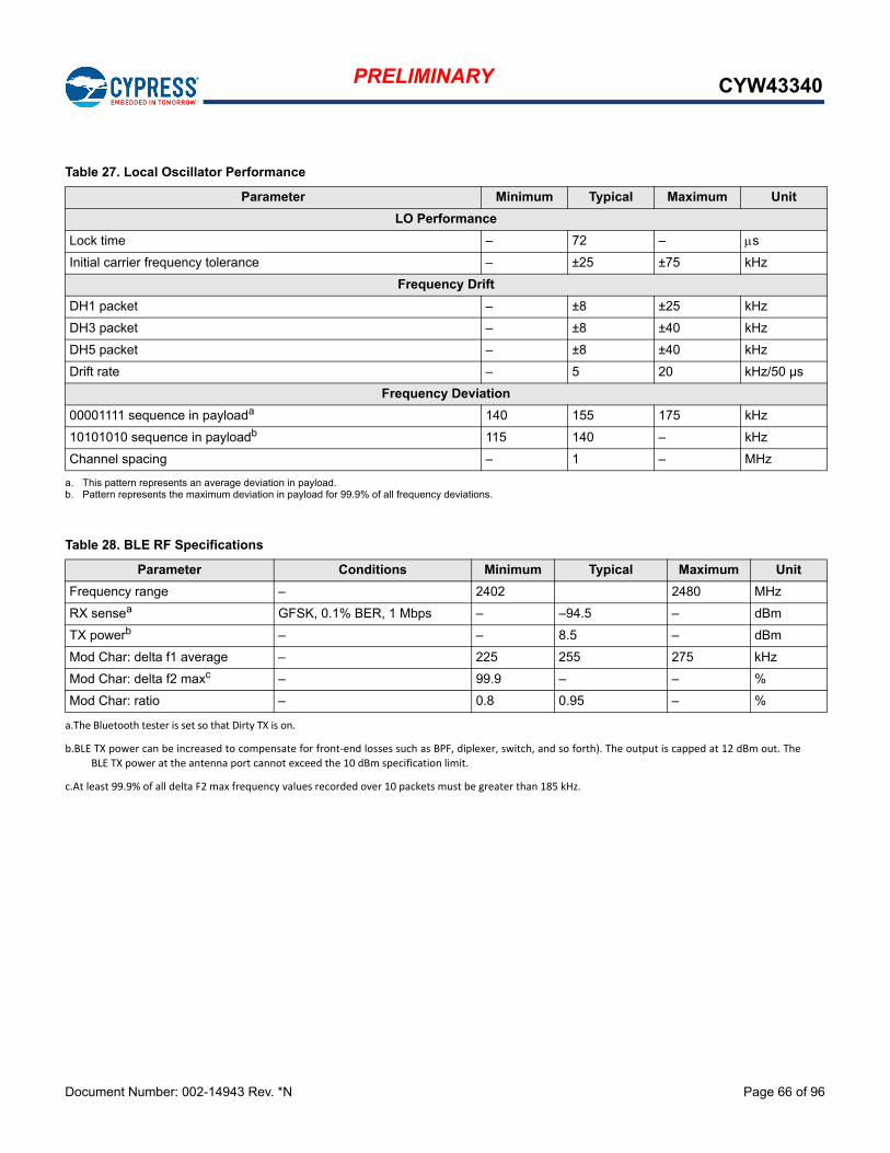
Document Number: 002-14943 Rev. *N Page 66 of 96
PRELIMINARY CYW43340
Table 27. Local Oscillator Performance
Parameter Minimum Typical Maximum Unit
LO Performance
Lock time – 72 – s
Initial carrier frequency tolerance – ±25 ±75 kHz
Frequency Drift
DH1 packet – ±8 ±25 kHz
DH3 packet – ±8 ±40 kHz
DH5 packet – ±8 ±40 kHz
Drift rate – 5 20 kHz/50 µs
Frequency Deviation
00001111 sequence in payloada
a. This pattern represents an average deviation in payload.
140 155 175 kHz
10101010 sequence in payloadb
b. Pattern represents the maximum deviation in payload for 99.9% of all frequency deviations.
115 140 – kHz
Channel spacing – 1 – MHz
Table 28. BLE RF Specifications
Parameter Conditions Minimum Typical Maximum Unit
Frequency range – 2402 2480 MHz
RX sensea
a.The Bluetooth tester is set so that Dirty TX is on.
GFSK, 0.1% BER, 1 Mbps – –94.5 – dBm
TX powerb
b.BLE TX power can be increased to compensate for front-end losses such as BPF, diplexer, switch, and so forth). The output is capped at 12 dBm out. The
BLE TX power at the antenna port cannot exceed the 10 dBm specification limit.
– – 8.5 – dBm
Mod Char: delta f1 average – 225 255 275 kHz
Mod Char: delta f2 maxc
c.At least 99.9% of all delta F2 max frequency values recorded over 10 packets must be greater than 185 kHz.
– 99.9 – – %
Mod Char: ratio – 0.8 0.95 – %
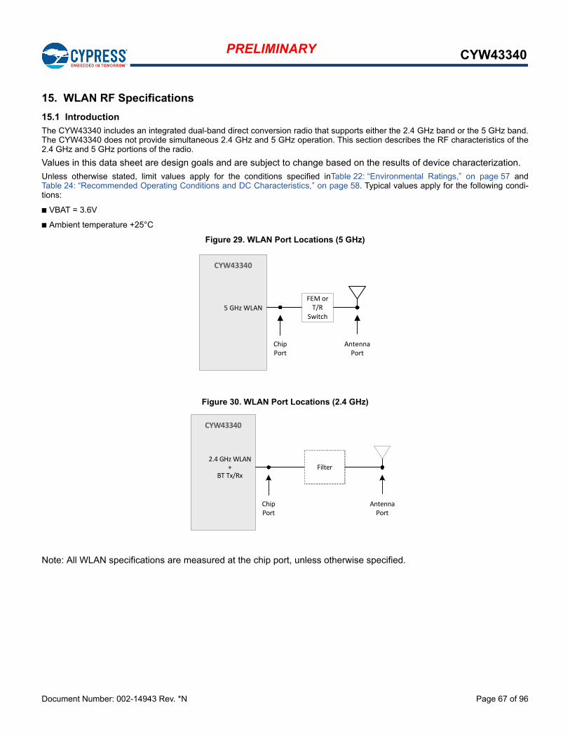
Document Number: 002-14943 Rev. *N Page 67 of 96
PRELIMINARY CYW43340
15. WLAN RF Specifications
15.1 Introduction
The CYW43340 includes an integrated dual-band direct conversion radio that supports either the 2.4 GHz band or the 5 GHz band.The CYW43340 does not provide simultaneous 2.4 GHz and 5 GHz operation. This section describes the RF characteristics of the2.4 GHz and 5 GHz portions of the radio.
Values in this data sheet are design goals and are subject to change based on the results of device characterization.
Unless otherwise stated, limit values apply for the conditions specified inTable 22: “Environmental Ratings,” on page 57 andTable 24: “Recommended Operating Conditions and DC Characteristics,” on page 58. Typical values apply for the following condi-tions:
VBAT = 3.6V
Ambient temperature +25°C
Figure 29. WLAN Port Locations (5 GHz)
Figure 30. WLAN Port Locations (2.4 GHz)
Note: All WLAN specifications are measured at the chip port, unless otherwise specified.
CYW43340
Antenna Port
5 GHz WLAN
ChipPort
FEM orT/R
Switch
CYW43340
Antenna Port
2.4 GHz WLAN+
BT Tx/Rx
ChipPort
Filter
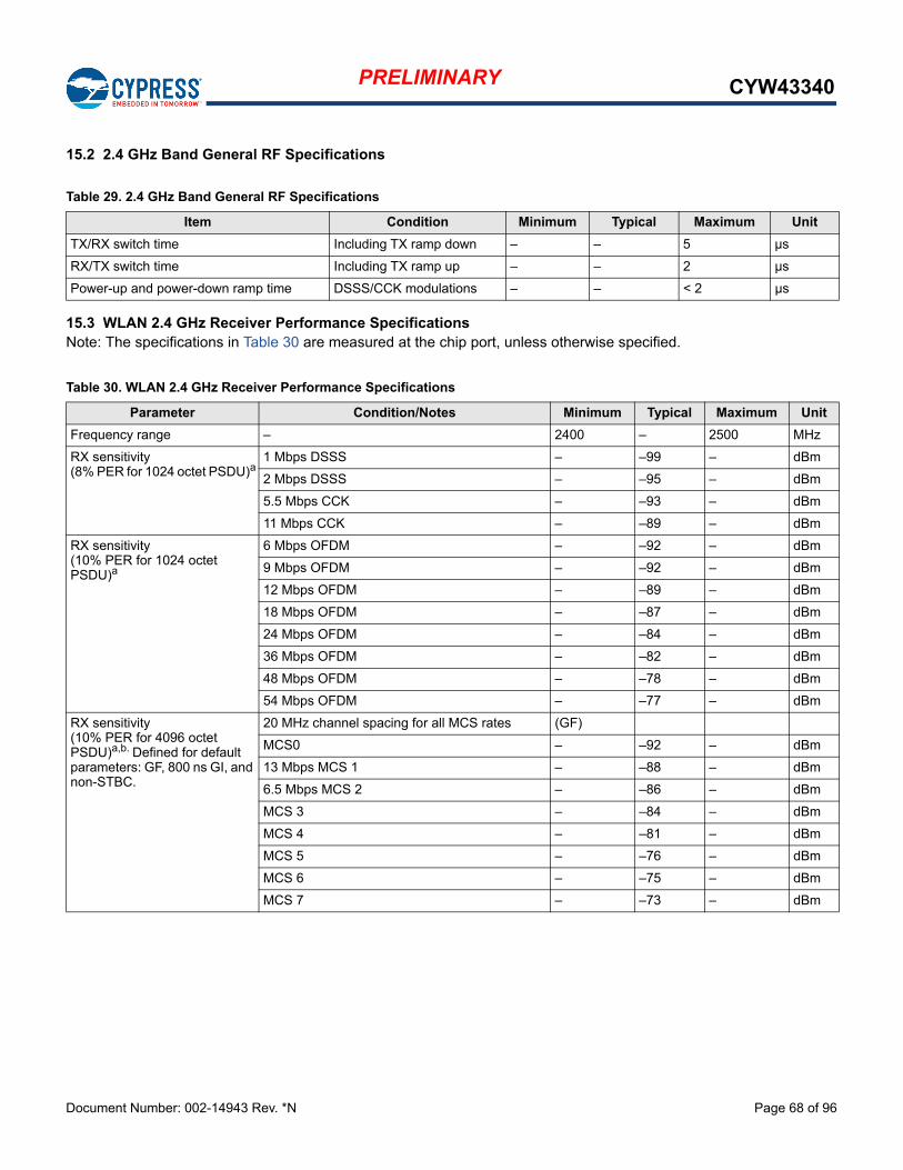
Document Number: 002-14943 Rev. *N Page 68 of 96
PRELIMINARY CYW43340
15.2 2.4 GHz Band General RF Specifications
15.3 WLAN 2.4 GHz Receiver Performance Specifications Note: The specifications in Table 30 are measured at the chip port, unless otherwise specified.
Table 29. 2.4 GHz Band General RF Specifications
Item Condition Minimum Typical Maximum Unit
TX/RX switch time Including TX ramp down – – 5 µs
RX/TX switch time Including TX ramp up – – 2 µs
Power-up and power-down ramp time DSSS/CCK modulations – – < 2 µs
Table 30. WLAN 2.4 GHz Receiver Performance Specifications
Parameter Condition/Notes Minimum Typical Maximum Unit
Frequency range – 2400 – 2500 MHz
RX sensitivity(8% PER for 1024 octet PSDU)a
1 Mbps DSSS – –99 – dBm
2 Mbps DSSS – –95 – dBm
5.5 Mbps CCK – –93 – dBm
11 Mbps CCK – –89 – dBm
RX sensitivity(10% PER for 1024 octet PSDU)a
6 Mbps OFDM – –92 – dBm
9 Mbps OFDM – –92 – dBm
12 Mbps OFDM – –89 – dBm
18 Mbps OFDM – –87 – dBm
24 Mbps OFDM – –84 – dBm
36 Mbps OFDM – –82 – dBm
48 Mbps OFDM – –78 – dBm
54 Mbps OFDM – –77 – dBm
RX sensitivity(10% PER for 4096 octet PSDU)a,b. Defined for default parameters: GF, 800 ns GI, and non-STBC.
20 MHz channel spacing for all MCS rates (GF)
MCS0 – –92 – dBm
13 Mbps MCS 1 – –88 – dBm
6.5 Mbps MCS 2 – –86 – dBm
MCS 3 – –84 – dBm
MCS 4 – –81 – dBm
MCS 5 – –76 – dBm
MCS 6 – –75 – dBm
MCS 7 – –73 – dBm
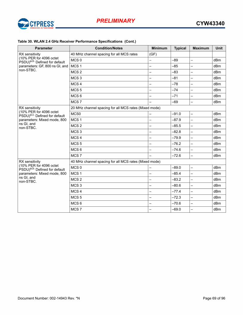
Document Number: 002-14943 Rev. *N Page 69 of 96
PRELIMINARY CYW43340
RX sensitivity(10% PER for 4096 octet PSDU)a,b. Defined for default parameters: GF, 800 ns GI, and non-STBC.
40 MHz channel spacing for all MCS rates (GF)
MCS 0 – –89 – dBm
MCS 1 – –85 – dBm
MCS 2 – –83 – dBm
MCS 3 – –81 – dBm
MCS 4 – –78 – dBm
MCS 5 – –74 – dBm
MCS 6 – –71 – dBm
MCS 7 – –69 – dBm
RX sensitivity(10% PER for 4096 octet PSDU)a,c. Defined for default parameters: Mixed mode, 800 ns GI, and non-STBC.
20 MHz channel spacing for all MCS rates (Mixed mode)
MCS0 – –91.0 – dBm
MCS 1 – –87.9 – dBm
MCS 2 – –85.5 – dBm
MCS 3 – –82.8 – dBm
MCS 4 – –79.9 – dBm
MCS 5 – –76.2 – dBm
MCS 6 – –74.6 – dBm
MCS 7 – –72.6 – dBm
RX sensitivity(10% PER for 4096 octet PSDU)a,b. Defined for default parameters: Mixed mode, 800 ns GI, and non-STBC.
40 MHz channel spacing for all MCS rates (Mixed mode)
MCS 0 – –89.0 – dBm
MCS 1 – –85.4 – dBm
MCS 2 – –83.2 – dBm
MCS 3 – –80.6 – dBm
MCS 4 – –77.4 – dBm
MCS 5 – –72.3 – dBm
MCS 6 – –70.6 – dBm
MCS 7 – –69.0 – dBm
Table 30. WLAN 2.4 GHz Receiver Performance Specifications (Cont.)
Parameter Condition/Notes Minimum Typical Maximum Unit
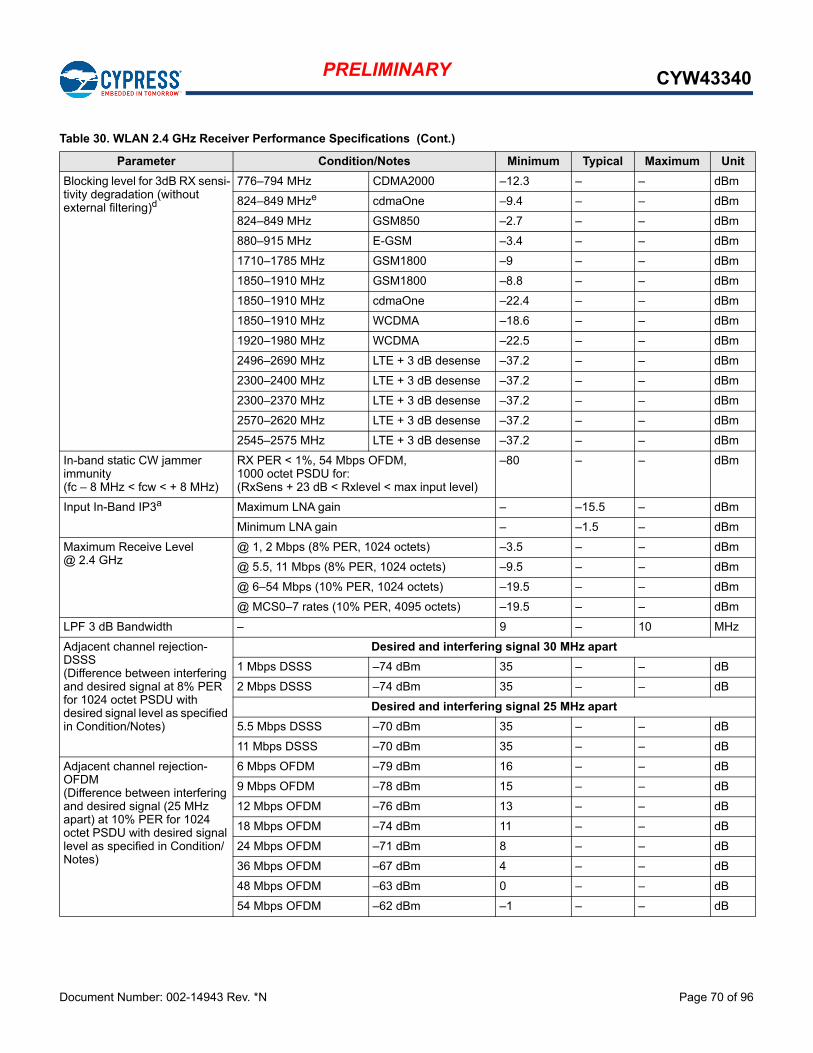
Document Number: 002-14943 Rev. *N Page 70 of 96
PRELIMINARY CYW43340
Blocking level for 3dB RX sensi-tivity degradation (without external filtering)d
776–794 MHz CDMA2000 –12.3 – – dBm
824–849 MHze cdmaOne –9.4 – – dBm
824–849 MHz GSM850 –2.7 – – dBm
880–915 MHz E-GSM –3.4 – – dBm
1710–1785 MHz GSM1800 –9 – – dBm
1850–1910 MHz GSM1800 –8.8 – – dBm
1850–1910 MHz cdmaOne –22.4 – – dBm
1850–1910 MHz WCDMA –18.6 – – dBm
1920–1980 MHz WCDMA –22.5 – – dBm
2496–2690 MHz LTE + 3 dB desense –37.2 – – dBm
2300–2400 MHz LTE + 3 dB desense –37.2 – – dBm
2300–2370 MHz LTE + 3 dB desense –37.2 – – dBm
2570–2620 MHz LTE + 3 dB desense –37.2 – – dBm
2545–2575 MHz LTE + 3 dB desense –37.2 – – dBm
In-band static CW jammer immunity(fc – 8 MHz < fcw < + 8 MHz)
RX PER < 1%, 54 Mbps OFDM, 1000 octet PSDU for: (RxSens + 23 dB < Rxlevel < max input level)
–80 – – dBm
Input In-Band IP3a Maximum LNA gain – –15.5 – dBm
Minimum LNA gain – –1.5 – dBm
Maximum Receive Level@ 2.4 GHz
@ 1, 2 Mbps (8% PER, 1024 octets) –3.5 – – dBm
@ 5.5, 11 Mbps (8% PER, 1024 octets) –9.5 – – dBm
@ 6–54 Mbps (10% PER, 1024 octets) –19.5 – – dBm
@ MCS0–7 rates (10% PER, 4095 octets) –19.5 – – dBm
LPF 3 dB Bandwidth – 9 – 10 MHz
Adjacent channel rejection-DSSS(Difference between interfering and desired signal at 8% PER for 1024 octet PSDU with desired signal level as specified in Condition/Notes)
Desired and interfering signal 30 MHz apart
1 Mbps DSSS –74 dBm 35 – – dB
2 Mbps DSSS –74 dBm 35 – – dB
Desired and interfering signal 25 MHz apart
5.5 Mbps DSSS –70 dBm 35 – – dB
11 Mbps DSSS –70 dBm 35 – – dB
Adjacent channel rejection-OFDM(Difference between interfering and desired signal (25 MHz apart) at 10% PER for 1024 octet PSDU with desired signal level as specified in Condition/Notes)
6 Mbps OFDM –79 dBm 16 – – dB
9 Mbps OFDM –78 dBm 15 – – dB
12 Mbps OFDM –76 dBm 13 – – dB
18 Mbps OFDM –74 dBm 11 – – dB
24 Mbps OFDM –71 dBm 8 – – dB
36 Mbps OFDM –67 dBm 4 – – dB
48 Mbps OFDM –63 dBm 0 – – dB
54 Mbps OFDM –62 dBm –1 – – dB
Table 30. WLAN 2.4 GHz Receiver Performance Specifications (Cont.)
Parameter Condition/Notes Minimum Typical Maximum Unit
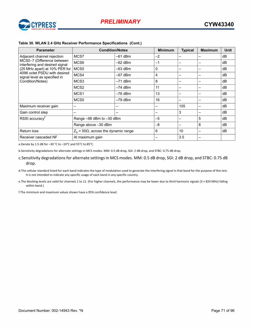
Document Number: 002-14943 Rev. *N Page 71 of 96
PRELIMINARY CYW43340
Adjacent channel rejection MCS0–7 (Difference between interfering and desired signal (25 MHz apart) at 10% PER for 4096 octet PSDU with desired signal level as specified in Condition/Notes)
MCS7 –61 dBm –2 – – dB
MCS6 –62 dBm –1 – – dB
MCS5 –63 dBm 0 – – dB
MCS4 –67 dBm 4 – – dB
MCS3 –71 dBm 8 – – dB
MCS2 –74 dBm 11 – – dB
MCS1 –76 dBm 13 – – dB
MCS0 –79 dBm 16 – – dB
Maximum receiver gain – – – 105 – dB
Gain control step – – – 3 – dB
RSSI accuracyf Range –98 dBm to –30 dBm –5 – 5 dB
Range above –30 dBm –8 – 8 dB
Return loss Zo = 50Ω, across the dynamic range 6 10 – dB
Receiver cascaded NF At maximum gain – 3.5 –
a.Derate by 1.5 dB for –30 °C to –10°C and 55°C to 85°C.
b.Sensitivity degradations for alternate settings in MCS modes. MM: 0.5 dB drop, SGI: 2 dB drop, and STBC: 0.75 dB drop.
c.Sensitivity degradations for alternate settings in MCS modes. MM: 0.5 dB drop, SGI: 2 dB drop, and STBC: 0.75 dBdrop.
d.The cellular standard listed for each band indicates the type of modulation used to generate the interfering signal in that band for the purpose of this test.
It is not intended to indicate any specific usage of each band in any specific country.
e.The blocking levels are valid for channels 1 to 11. (For higher channels, the performance may be lower due to third harmonic signals (3 × 824 MHz) fallingwithin band.)
f.The minimum and maximum values shown have a 95% confidence level.
Table 30. WLAN 2.4 GHz Receiver Performance Specifications (Cont.)
Parameter Condition/Notes Minimum Typical Maximum Unit
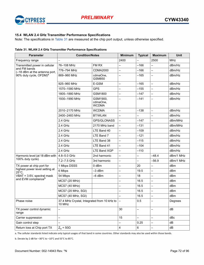
Document Number: 002-14943 Rev. *N Page 72 of 96
PRELIMINARY CYW43340
15.4 WLAN 2.4 GHz Transmitter Performance SpecificationsNote: The specifications in Table 31 are measured at the chip port output, unless otherwise specified.
Table 31. WLAN 2.4 GHz Transmitter Performance Specifications
Parameter Condition/Notes Minimum Typical Maximum Unit
Frequency range – 2400 – 2500 MHz
Transmitted power in cellular and FM bands (–18 dBm at the antenna port, 90% duty cycle, OFDM)a
a. The cellular standards listed indicate only typical usages of that band in some countries. Other standards may also be used within those bands.
76–108 MHz FM RX – –166 – dBm/Hz
776–794 MHz CDMA2000 – –166 – dBm/Hz
869–960 MHz cdmaOne, GSM850
– –165 – dBm/Hz
925–960 MHz E-GSM – –165 – dBm/Hz
1570–1580 MHz GPS – –155 – dBm/Hz
1805–1880 MHz GSM1800 – –147 – dBm/Hz
1930–1990 MHz GSM1900, cdmaOne, WCDMA
– –141 – dBm/Hz
2010–2170 MHz WCDMA – –138 – dBm/Hz
2400–2483 MHz BT/WLAN – – – dBm/Hz
2.4 GHz GPS/GLONASS – –147 – dBm/MHz
2.4 GHz 2170 MHz band – –131 dBm/MHz
2.4 GHz LTE Band 40 – –109 dBm/Hz
2.4 GHz LTE Band 7 – –121 dBm/Hz
2.4 GHz LTE Band 38 – –115 dBm/Hz
2.4 GHz LTE Band 41 – –104 dBm/Hz
2.4 GHz LTE Band XGP – –110 dBm/Hz
Harmonic level (at 18 dBm with 100% duty cycle)
4.8–5.0 GHz 2nd harmonic – – –48.4 dBm/1 MHz
7.2–7.5 GHz 3rd harmonic – – –56.9 dBm/1 MHz
TX power at chip port for highest power level setting at 25°C, VBAT = 3.6V, spectral mask and EVM complianceb
b. Derate by 2 dB for –30°C to –10°C and 55°C to 85°C.
1 Mbps DSSS 0 dBm – 20 – dBm
6 Mbps –3 dBm – 19.5 – dBm
54 Mbps –6 dBm – 18 – dBm
MCS7 (20 MHz) – 16.5 – dBm
MCS7 (40 MHz) – 16.5 – dBm
MCS7 (20 MHz, SGI) – 16.5 – dBm
MCS7 (40 MHz, SGI) – 16.5 – dBm
Phase noise 37.4 MHz Crystal, Integrated from 10 kHz to 10 MHz
– 0.5 – Degrees
TX power control dynamic range
– 30 – – dB
Carrier suppression – 15 – – dBc
Gain control step – – 0.25 – dB
Return loss at Chip port TX Zo = 50Ω 4 6 – dB
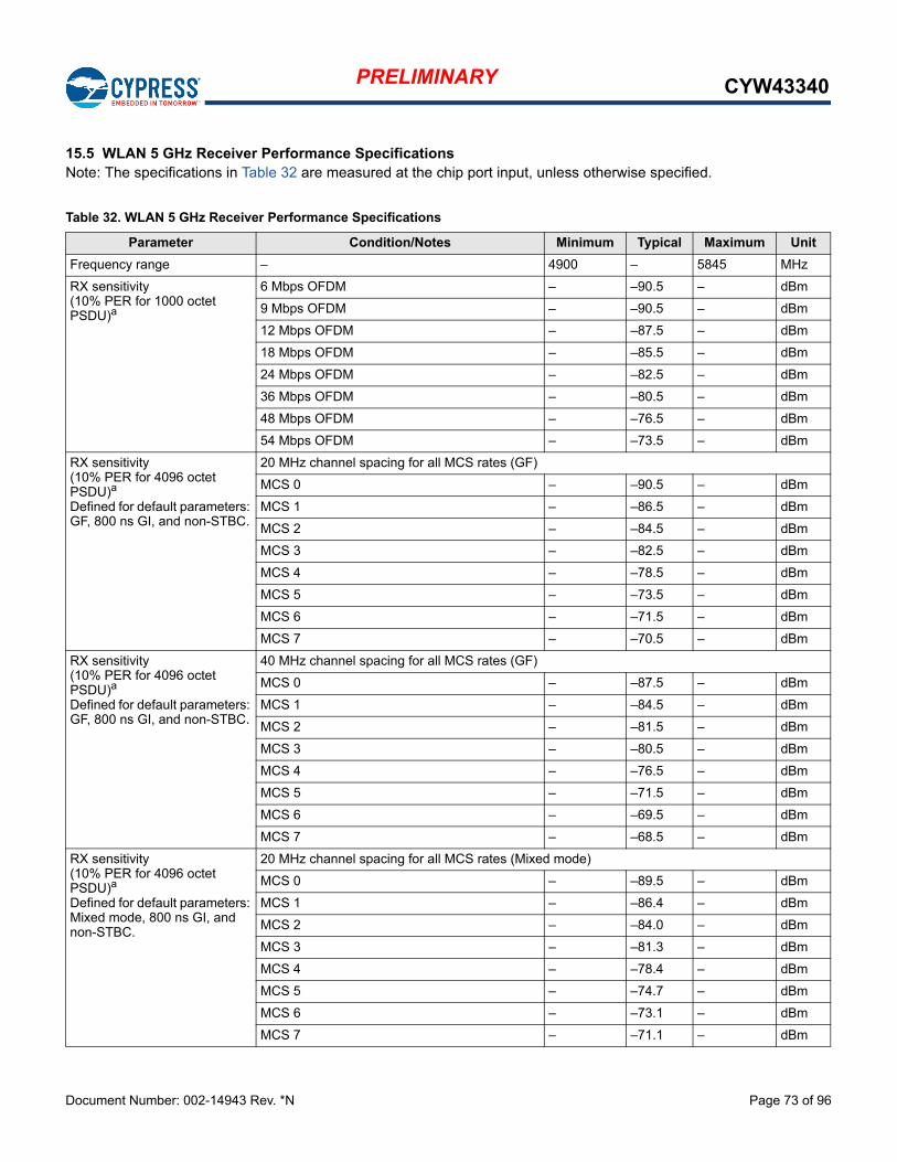
Document Number: 002-14943 Rev. *N Page 73 of 96
PRELIMINARY CYW43340
15.5 WLAN 5 GHz Receiver Performance Specifications Note: The specifications in Table 32 are measured at the chip port input, unless otherwise specified.
Table 32. WLAN 5 GHz Receiver Performance Specifications
Parameter Condition/Notes Minimum Typical Maximum Unit
Frequency range – 4900 – 5845 MHz
RX sensitivity(10% PER for 1000 octet PSDU)a
6 Mbps OFDM – –90.5 – dBm
9 Mbps OFDM – –90.5 – dBm
12 Mbps OFDM – –87.5 – dBm
18 Mbps OFDM – –85.5 – dBm
24 Mbps OFDM – –82.5 – dBm
36 Mbps OFDM – –80.5 – dBm
48 Mbps OFDM – –76.5 – dBm
54 Mbps OFDM – –73.5 – dBm
RX sensitivity (10% PER for 4096 octet PSDU)a
Defined for default parameters: GF, 800 ns GI, and non-STBC.
20 MHz channel spacing for all MCS rates (GF)
MCS 0 – –90.5 – dBm
MCS 1 – –86.5 – dBm
MCS 2 – –84.5 – dBm
MCS 3 – –82.5 – dBm
MCS 4 – –78.5 – dBm
MCS 5 – –73.5 – dBm
MCS 6 – –71.5 – dBm
MCS 7 – –70.5 – dBm
RX sensitivity (10% PER for 4096 octet PSDU)a
Defined for default parameters: GF, 800 ns GI, and non-STBC.
40 MHz channel spacing for all MCS rates (GF)
MCS 0 – –87.5 – dBm
MCS 1 – –84.5 – dBm
MCS 2 – –81.5 – dBm
MCS 3 – –80.5 – dBm
MCS 4 – –76.5 – dBm
MCS 5 – –71.5 – dBm
MCS 6 – –69.5 – dBm
MCS 7 – –68.5 – dBm
RX sensitivity (10% PER for 4096 octet PSDU)a
Defined for default parameters: Mixed mode, 800 ns GI, and non-STBC.
20 MHz channel spacing for all MCS rates (Mixed mode)
MCS 0 – –89.5 – dBm
MCS 1 – –86.4 – dBm
MCS 2 – –84.0 – dBm
MCS 3 – –81.3 – dBm
MCS 4 – –78.4 – dBm
MCS 5 – –74.7 – dBm
MCS 6 – –73.1 – dBm
MCS 7 – –71.1 – dBm
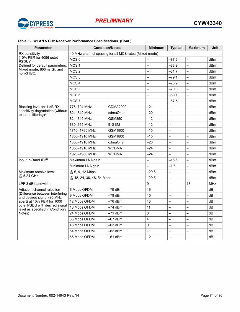
Document Number: 002-14943 Rev. *N Page 74 of 96
PRELIMINARY CYW43340
RX sensitivity (10% PER for 4096 octet PSDU)a
Defined for default parameters: Mixed mode, 800 ns GI, and non-STBC.
40 MHz channel spacing for all MCS rates (Mixed mode)
MCS 0 – –87.5 – dBm
MCS 1 – –83.9 – dBm
MCS 2 – –81.7 – dBm
MCS 3 – –79.1 – dBm
MCS 4 – –75.9 – dBm
MCS 5 – –70.8 – dBm
MCS 6 – –69.1 – dBm
MCS 7 – –67.5 – dBm
Blocking level for 1 dB RX sensitivity degradation (without external filtering)b
776–794 MHz CDMA2000 –21 – – dBm
824–849 MHz cdmaOne –20 – – dBm
824–849 MHz GSM850 –12 – – dBm
880–915 MHz E-GSM –12 – – dBm
1710–1785 MHz GSM1800 –15 – – dBm
1850–1910 MHz GSM1800 –15 – – dBm
1850–1910 MHz cdmaOne –20 – – dBm
1850–1910 MHz WCDMA –24 – – dBm
1920–1980 MHz WCDMA –24 – – dBm
Input In-Band IP3a Maximum LNA gain – –15.5 – dBm
Minimum LNA gain – –1.5 – dBm
Maximum receive level@ 5.24 GHz
@ 6, 9, 12 Mbps –29.5 – – dBm
@ 18, 24, 36, 48, 54 Mbps –29.5 – – dBm
LPF 3 dB bandwidth – 9 – 18 MHz
Adjacent channel rejection(Difference between interfering and desired signal (20 MHz apart) at 10% PER for 1000 octet PSDU with desired signal level as specified in Condition/Notes)
6 Mbps OFDM –79 dBm 16 – – dB
9 Mbps OFDM –78 dBm 15 – – dB
12 Mbps OFDM –76 dBm 13 – – dB
18 Mbps OFDM –74 dBm 11 – – dB
24 Mbps OFDM –71 dBm 8 – – dB
36 Mbps OFDM –67 dBm 4 – – dB
48 Mbps OFDM –63 dBm 0 – – dB
54 Mbps OFDM –62 dBm –1 – – dB
65 Mbps OFDM –61 dBm –2 – – dB
Table 32. WLAN 5 GHz Receiver Performance Specifications (Cont.)
Parameter Condition/Notes Minimum Typical Maximum Unit
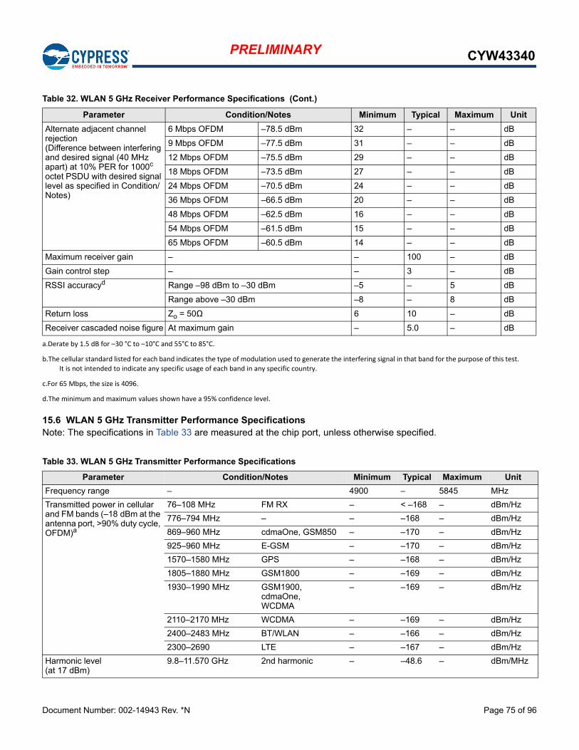
Document Number: 002-14943 Rev. *N Page 75 of 96
PRELIMINARY CYW43340
15.6 WLAN 5 GHz Transmitter Performance Specifications Note: The specifications in Table 33 are measured at the chip port, unless otherwise specified.
Alternate adjacent channel rejection(Difference between interfering and desired signal (40 MHz apart) at 10% PER for 1000c octet PSDU with desired signal level as specified in Condition/Notes)
6 Mbps OFDM –78.5 dBm 32 – – dB
9 Mbps OFDM –77.5 dBm 31 – – dB
12 Mbps OFDM –75.5 dBm 29 – – dB
18 Mbps OFDM –73.5 dBm 27 – – dB
24 Mbps OFDM –70.5 dBm 24 – – dB
36 Mbps OFDM –66.5 dBm 20 – – dB
48 Mbps OFDM –62.5 dBm 16 – – dB
54 Mbps OFDM –61.5 dBm 15 – – dB
65 Mbps OFDM –60.5 dBm 14 – – dB
Maximum receiver gain – – 100 – dB
Gain control step – – 3 – dB
RSSI accuracyd Range –98 dBm to –30 dBm –5 – 5 dB
Range above –30 dBm –8 – 8 dB
Return loss Zo = 50Ω 6 10 – dB
Receiver cascaded noise figure At maximum gain – 5.0 – dB
a.Derate by 1.5 dB for –30 °C to –10°C and 55°C to 85°C.
b.The cellular standard listed for each band indicates the type of modulation used to generate the interfering signal in that band for the purpose of this test.
It is not intended to indicate any specific usage of each band in any specific country.
c.For 65 Mbps, the size is 4096.
d.The minimum and maximum values shown have a 95% confidence level.
Table 33. WLAN 5 GHz Transmitter Performance Specifications
Parameter Condition/Notes Minimum Typical Maximum Unit
Frequency range – 4900 – 5845 MHz
Transmitted power in cellular and FM bands (–18 dBm at the antenna port, >90% duty cycle, OFDM)a
76–108 MHz FM RX – < –168 – dBm/Hz
776–794 MHz – – –168 – dBm/Hz
869–960 MHz cdmaOne, GSM850 – –170 – dBm/Hz
925–960 MHz E-GSM – –170 – dBm/Hz
1570–1580 MHz GPS – –168 – dBm/Hz
1805–1880 MHz GSM1800 – –169 – dBm/Hz
1930–1990 MHz GSM1900,cdmaOne,WCDMA
– –169 – dBm/Hz
2110–2170 MHz WCDMA – –169 – dBm/Hz
2400–2483 MHz BT/WLAN – –166 – dBm/Hz
2300–2690 LTE – –167 – dBm/Hz
Harmonic level (at 17 dBm)
9.8–11.570 GHz 2nd harmonic – –48.6 – dBm/MHz
Table 32. WLAN 5 GHz Receiver Performance Specifications (Cont.)
Parameter Condition/Notes Minimum Typical Maximum Unit
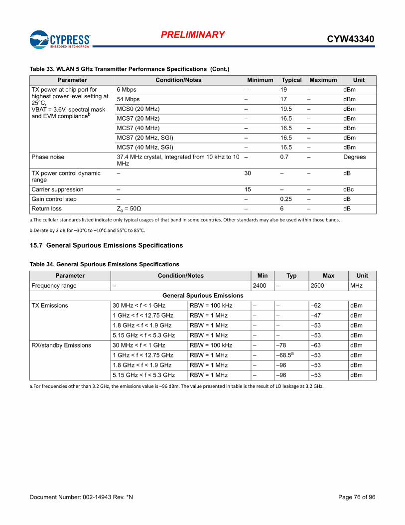
Document Number: 002-14943 Rev. *N Page 76 of 96
PRELIMINARY CYW43340
15.7 General Spurious Emissions Specifications
TX power at chip port for highest power level setting at 25°C, VBAT = 3.6V, spectral mask and EVM complianceb
6 Mbps – 19 – dBm
54 Mbps – 17 – dBm
MCS0 (20 MHz) – 19.5 – dBm
MCS7 (20 MHz) – 16.5 – dBm
MCS7 (40 MHz) – 16.5 – dBm
MCS7 (20 MHz, SGI) – 16.5 – dBm
MCS7 (40 MHz, SGI) – 16.5 – dBm
Phase noise 37.4 MHz crystal, Integrated from 10 kHz to 10 MHz
– 0.7 – Degrees
TX power control dynamic range
– 30 – – dB
Carrier suppression – 15 – – dBc
Gain control step – – 0.25 – dB
Return loss Zo = 50Ω – 6 – dB
a.The cellular standards listed indicate only typical usages of that band in some countries. Other standards may also be used within those bands.
b.Derate by 2 dB for –30°C to –10°C and 55°C to 85°C.
Table 34. General Spurious Emissions Specifications
Parameter Condition/Notes Min Typ Max Unit
Frequency range – 2400 – 2500 MHz
General Spurious Emissions
TX Emissions 30 MHz < f < 1 GHz RBW = 100 kHz – – –62 dBm
1 GHz < f < 12.75 GHz RBW = 1 MHz – – –47 dBm
1.8 GHz < f < 1.9 GHz RBW = 1 MHz – – –53 dBm
5.15 GHz < f < 5.3 GHz RBW = 1 MHz – – –53 dBm
RX/standby Emissions 30 MHz < f < 1 GHz RBW = 100 kHz – –78 –63 dBm
1 GHz < f < 12.75 GHz RBW = 1 MHz – –68.5a
a.For frequencies other than 3.2 GHz, the emissions value is –96 dBm. The value presented in table is the result of LO leakage at 3.2 GHz.
–53 dBm
1.8 GHz < f < 1.9 GHz RBW = 1 MHz – –96 –53 dBm
5.15 GHz < f < 5.3 GHz RBW = 1 MHz – –96 –53 dBm
Table 33. WLAN 5 GHz Transmitter Performance Specifications (Cont.)
Parameter Condition/Notes Minimum Typical Maximum Unit
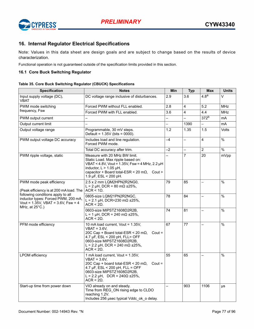
Document Number: 002-14943 Rev. *N Page 77 of 96
PRELIMINARY CYW43340
16. Internal Regulator Electrical Specifications
Note: Values in this data sheet are design goals and are subject to change based on the results of devicecharacterization.
Functional operation is not guaranteed outside of the specification limits provided in this section.
16.1 Core Buck Switching Regulator
Table 35. Core Buck Switching Regulator (CBUCK) Specifications
Specification Notes Min Typ Max Units
Input supply voltage (DC), VBAT
DC voltage range inclusive of disturbances. 2.9 3.6 4.8a V
PWM mode switching frequency, Fsw
Forced PWM without FLL enabled. 2.8 4 5.2 MHz
Forced PWM with FLL enabled. 3.6 4 4.4 MHz
PWM output current – – – 372b mA
Output current limit – – 1390 – mA
Output voltage range Programmable, 30 mV steps.Default = 1.35V (bits = 0000).
1.2 1.35 1.5 Volts
PWM output voltage DC accuracy Includes load and line regulation. Forced PWM mode.
–4 – 4 %
Total DC accuracy after trim. –2 – 2 %
PWM ripple voltage, static Measure with 20 MHz BW limit.Static Load. Max ripple based on:VBAT < 4.8V, Vout = 1.35V, Fsw = 4 MHz, 2.2 µH inductor, L > 1.05 µH, capacitor + Board total-ESR < 20 mΩ, Cout > 1.9 µF, ESL < 200 pH.
– 7 20 mVpp
PWM mode peak efficiency
(Peak efficiency is at 200 mA load. The following conditions apply to all inductor types: Forced PWM, 200 mA, Vout = 1.35V, VBAT = 3.6V, Fsw = 4 MHz, at 25°C.)
2.5 x 2 mm LQM2HPN2R2NG0,L = 2 µH, DCR = 80 mΩ ±25%, ACR < 1Ω.
79 85 – %
0805-size LQM21PN2R2NGC,L = 2.1 µH, DCR=230 mΩ ±25%,ACR < 2Ω.
78 84 – %
0603-size MIPSTZ1608D2R2B,L = 1 µH, DCR = 240 mΩ ±25%,ACR < 2Ω.
74 81 – %
PFM mode efficiency 10 mA load current, Vout = 1.35V, VBAT = 3.6V, 20C Cap + Board total-ESR < 20 mΩ, Cout = 4.7 µF, ESL < 200 pH, FLL= OFF0603-size MIPSTZ1608D2R2B, L = 2.2 µH, DCR = 240 mΩ ±25%,ACR < 2Ω.
67 77 – %
LPOM efficiency 1 mA load current, Vout = 1.35V, VBAT = 3.6V, 20C Cap + board total-ESR < 20 mΩ, Cout = 4.7 µF, ESL < 200 pH, FLL = OFF0603-size MIPSTZ1608D2R2B,L = 2.2 µH, DCR = 240Ω ±25%,ACR < 2Ω.
55 65 – %
Start-up time from power down VIO already on and steady.Time from REG_ON rising edge to CLDO reaching 1.2V.Includes 256 µsec typical Vddc_ok_o delay.
– 903 1106 µs
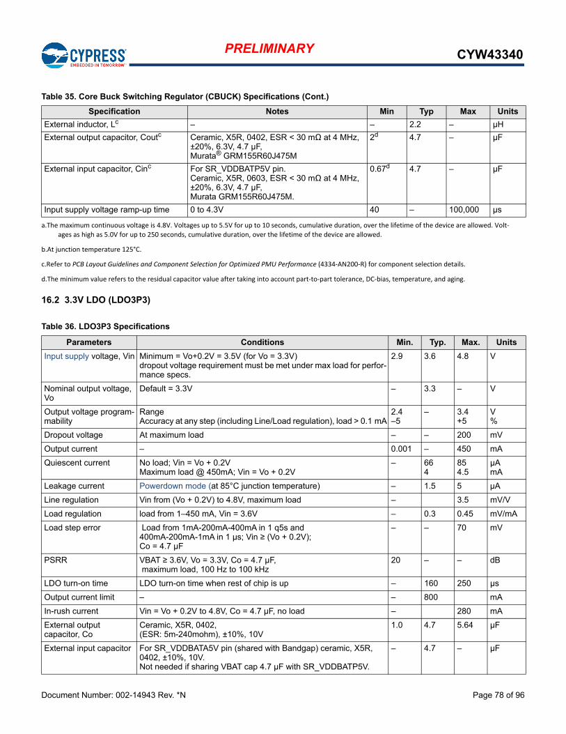
Document Number: 002-14943 Rev. *N Page 78 of 96
PRELIMINARY CYW43340
16.2 3.3V LDO (LDO3P3)
External inductor, Lc – – 2.2 – µH
External output capacitor, Coutc Ceramic, X5R, 0402, ESR < 30 mΩ at 4 MHz, ±20%, 6.3V, 4.7 µF, Murata® GRM155R60J475M
2d 4.7 – µF
External input capacitor, Cinc For SR_VDDBATP5V pin. Ceramic, X5R, 0603, ESR < 30 mΩ at 4 MHz, ±20%, 6.3V, 4.7 µF, Murata GRM155R60J475M.
0.67d 4.7 – µF
Input supply voltage ramp-up time 0 to 4.3V 40 – 100,000 µs
a.The maximum continuous voltage is 4.8V. Voltages up to 5.5V for up to 10 seconds, cumulative duration, over the lifetime of the device are allowed. Volt-
ages as high as 5.0V for up to 250 seconds, cumulative duration, over the lifetime of the device are allowed.
b.At junction temperature 125°C.
c.Refer to PCB Layout Guidelines and Component Selection for Optimized PMU Performance (4334-AN200-R) for component selection details.
d.The minimum value refers to the residual capacitor value after taking into account part-to-part tolerance, DC-bias, temperature, and aging.
Table 36. LDO3P3 Specifications
Parameters Conditions Min. Typ. Max. Units
Input supply voltage, Vin Minimum = Vo+0.2V = 3.5V (for Vo = 3.3V)dropout voltage requirement must be met under max load for perfor-mance specs.
2.9 3.6 4.8 V
Nominal output voltage, Vo
Default = 3.3V – 3.3 – V
Output voltage program-mability
RangeAccuracy at any step (including Line/Load regulation), load > 0.1 mA
2.4–5
– 3.4+5
V%
Dropout voltage At maximum load – – 200 mV
Output current – 0.001 – 450 mA
Quiescent current No load; Vin = Vo + 0.2VMaximum load @ 450mA; Vin = Vo + 0.2V
– 664
854.5
µAmA
Leakage current Powerdown mode (at 85°C junction temperature) – 1.5 5 µA
Line regulation Vin from (Vo + 0.2V) to 4.8V, maximum load – 3.5 mV/V
Load regulation load from 1–450 mA, Vin = 3.6V – 0.3 0.45 mV/mA
Load step error Load from 1mA-200mA-400mA in 1 q5s and 400mA-200mA-1mA in 1 µs; Vin ≥ (Vo + 0.2V); Co = 4.7 µF
– – 70 mV
PSRR VBAT ≥ 3.6V, Vo = 3.3V, Co = 4.7 µF, maximum load, 100 Hz to 100 kHz
20 – – dB
LDO turn-on time LDO turn-on time when rest of chip is up – 160 250 µs
Output current limit – – 800 mA
In-rush current Vin = Vo + 0.2V to 4.8V, Co = 4.7 µF, no load – 280 mA
External output capacitor, Co
Ceramic, X5R, 0402, (ESR: 5m-240mohm), ±10%, 10V
1.0 4.7 5.64 µF
External input capacitor For SR_VDDBATA5V pin (shared with Bandgap) ceramic, X5R, 0402, ±10%, 10V. Not needed if sharing VBAT cap 4.7 µF with SR_VDDBATP5V.
– 4.7 – µF
Table 35. Core Buck Switching Regulator (CBUCK) Specifications (Cont.)
Specification Notes Min Typ Max Units
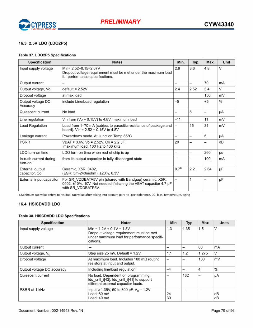
Document Number: 002-14943 Rev. *N Page 79 of 96
PRELIMINARY CYW43340
16.3 2.5V LDO (LDO2P5)
16.4 HSICDVDD LDO
Table 37. LDO2P5 Specifications
Specification Notes Min. Typ. Max. Unit
Input supply voltage Min= 2.52+0.15=2.67VDropout voltage requirement must be met under the maximum load for performance specifications.
2.9 3.6 4.8 V
Output current – – – 70 mA
Output voltage, Vo default = 2.52V 2.4 2.52 3.4 V
Dropout voltage at max load 150 mV
Output voltage DC Accuracy
include Line/Load regulation –5 +5 %
Quiescent current No load – 8 – µA
Line regulation Vin from (Vo + 0.15V) to 4.8V, maximum load –11 11 mV
Load Regulation Load from 1–70 mA (subject to parasitic resistance of package and board). Vin = 2.52 + 0.15V to 4.8V
– 15 31 mV
Leakage current Powerdown mode. At Junction Temp 85°C – – 5 µA
PSRR VBAT ≥ 3.6V, Vo = 2.52V, Co = 2.2 µF, maximum load, 100 Hz to 100 kHz
20 – – dB
LDO turn-on time LDO turn-on time when rest of chip is up – – 260 µs
In-rush current during turn-on
from its output capacitor in fully-discharged state – – 100 mA
External output capacitor, Co
Ceramic, X5R, 0402, (ESR: 5m-240mohm), ±20%, 6.3V
0.7a
a.Minimum cap value refers to residual cap value after taking into account part–to–part tolerance, DC–bias, temperature, aging
2.2 2.64 µF
External input capacitor For SR_VDDBATA5V pin (shared with Bandgap) ceramic, X5R, 0402, ±10%, 10V. Not needed if sharing the VBAT capacitor 4.7 µF with SR_VDDBATP5V.
– 1 – µF
Table 38. HISCDVDD LDO Specifications
Specification Notes Min Typ Max Units
Input supply voltage Min = 1.2V + 0.1V = 1.3V. Dropout voltage requirement must be met under maximum load for performance specifi-cations.
1.3 1.35 1.5 V
Output current – – – 80 mA
Output voltage, Vo Step size 25 mV. Default = 1.2V. 1.1 1.2 1.275 V
Dropout voltage At maximum load. Includes 100 mΩ routing resistors at input and output.
– – 100 mV
Output voltage DC accuracy Including line/load regulation. –4 – 4 %
Quiescent current No load. Dependent on programming. ldo_cntl_i[43], ldo_cntl_i[41] to support different external capacitor loads.
– 182 – µA
PSRR at 1 kHz Input ≥ 1.35V, 50 to 300 pF, Vo = 1.2VLoad: 80 mALoad: 40 mA
2439
– –dBdB
Document Number: 002-14943 Rev. *N Page 80 of 96
PRELIMINARY CYW43340
16.5 CLDO
PSRR at 10 kHz Input ≥ 1.35V, 50 to 300 pF, Vo = 1.2VLoad: 80 mALoad: 40 mA
2438
– –dBdB
PSRR at 100 kHz Input ≥ 1.35V, 50 to 300 pF, Vo = 1.2VLoad: 80 mALoad: 40 mA
1527
– –dBdB
Output Capacitor, Co Internal capacitor = Sum of supply decoupling caps and supply-to-ground routing parasitic capacitance.Output capacitor dependent on programming.
– 1000 – pF
Table 39. CLDO Specifications
Specification Notes Min Typ Max Units
Input supply voltage, Vin Min = 1.2 + 0.1V = 1.3V. Dropout voltage requirement must be met under maximum load.
1.3 1.35 1.5 V
Output current – 0.1 – 150 mA
Output voltage, Vo Programmable in 25 mV steps. Default = 1.2V, load from 0.1–150 mA
1.1 1.2 1.275 V
Dropout voltage At max load – – 100 mV
Output voltage DC accuracya
a.Load from 0.1 to 150 mA.
Includes line/load regulation –4 – +4 %
After trim, load from 0.1–150 mA, includes line/load regulation.Vin > Vo + 0.1V.
–2 – +2 %
Quiescent current No load – 10 – µA
Line regulation Vin from (Vo + 0.1V) to 1.5V, maximum load – – 7 mV/V
Load regulation Load from 1 mA to 150 mA – 15 25 µV/mA
Leakage current Power-down – – 10 µA
PSRR @1 kHz, Vin ≥ 1.5V, Co = 1 µF 20 – dB
Start-up time of PMU VIO up and steady. Time from the REG_ON rising edge to the CLDO reaching 1.2V. Includes 256 µs vddc_ok_o delay.
– – 1106 µs
LDO turn-on time Chip already powered up. – – 180 µs
In-rush current during turn-on From its output capacitor in a fully-discharged state – – 150 mA
External output capacitor, Cob
b.Refer to PCB Layout Guidelines and Component Selection for Optimized PMU Performance (4334-AN200-R) for component selection details.
Total ESR: 30 mΩ–200 mΩ 0.67c
c.The minimum value refers to the residual capacitor value after taking into account the part-to-part tolerance, DC-bias, temperature, and aging.
1 – µF
External input capacitor Only use an external input capacitor at the VDD_LDO pin if it is not supplied from the CBUCK output. Total ESR (trace/capacitor): 30 mΩ–200 mΩ
– 1 – µF
Table 38. HISCDVDD LDO Specifications (Cont.)
Specification Notes Min Typ Max Units
Document Number: 002-14943 Rev. *N Page 81 of 96
PRELIMINARY CYW43340
16.6 LNLDO
Table 40. LNLDO Specifications
Specification Notes Min Typ Max Units
Input supply voltage, Vin Min = 1.2Vo + 0.1V = 1.3V.Dropout voltage requirement must be met under maximum load.
1.3 1.35 1.5 V
Output current – 0.1 – 104 mA
Output voltage, Vo Programmable in 25 mV steps.Default = 1.2V
1.1 1.2 1.275 V
Dropout voltage At maximum load – – 100 mV
Output voltage DC accuracya
a.Load from 0.1 to 104 mA.
includes line/load regulation, load from 0.1 to 150 mA
–4 – +4 %
Quiescent current No load – 44 – µA
Line regulation Vin from (Vo + 0.1V) to 1.5V, max load – – 7 mV/V
Load regulation Load from 1 mA to 104 mA – 15 25 µV/mA
Leakage current Power-down – – 10 µA
Output noise @30 kHz, 60 mA load, Co = 1 µF @100 kHz, 60 mA load, Co = 1 µF
– – 60 35
nV/root-HznV/root-Hz
PSRR @ 1kHz, input > 1.3V, Co= 1 µF, Vo = 1.2V
20 – – dB
Start-up time of PMU VIO up and steady. Time from the REG_ON rising edge to the LNLDO reaching 1.2V. Includes 256 µs vddc_ok_o delay.
– – 1106 µs
LDO turn-on time Chip already powered up. – – 180 µs
In-rush current during turn-on From its output capacitor in a fully-discharged state
– – 150 mA
External output capacitor, Co
b
b.Refer to PCB Layout Guidelines and Component Selection for Optimized PMU Performance (4334-AN200-R) for component selection details.
Total ESR (trace/capacitor): 30–200 mΩ 0.67c
c.The minimum value refers to the residual capacitor value after taking into account the part-to-part tolerance, DC-bias, temperature, and aging.
1 – µF
External input capacitor Only use an external input capacitor at the VDD_LDO pin if it is not supplied from the CBUCK output. Total ESR (trace/capacitor): 30–200 mΩ
– 1 – µF
Document Number: 002-14943 Rev. *N Page 82 of 96
PRELIMINARY CYW43340
17. System Power Consumption
Note: Values in this data sheet are design goals and are subject to change based on the results of devicecharacterization.
Unless otherwise stated, these values apply for the conditions specified in Table 24: “Recommended Operating Conditions and DC Characteristics,” on page 58.
17.1 WLAN Current Consumption
The WLAN current consumption measurements are shown in Table 41.
All values in Table 41 are with the Bluetooth core in reset (that is, Bluetooth is off).
Table 41. Typical WLAN Power Consumption
Mode Bandwidth (MHz)
Band (GHz)
VBAT = 3.6V, VDDIO = 1.8V, TA 25°C
VBAT (mA) Vioa (µA)
a.Vio is specified with all pins idle and not driving any loads.
Sleep Modes
Leakage (OFF) – – 0.004 220
SLEEPb
b.Idle between beacons.
– – 0.005 220
IEEE Power Save, DTIM 1c
c.Beacon interval = 100 ms; beacon duration = 1.9 ms @ 1Mbps (Integrated Sleep + wakeup + beacon)
– – 1.06 220
IEEE Power Save DTIM 3d
d.Beacon interval = 300 ms; beacon duration = 1.9 ms @ 1Mbps (Integrated Sleep + wakeup + beacon)
– – 0.321 220
Active Modes
RX (Listen)e, f
e.Carrier sense (CCA) when no carrier present.
f.Carrier sense (CS) detect/packet RX.
– – 44.4 200
RX (Active)f, g, h
g.Applicable to all supported rates.
h.Duty Cycle = 100%
– – 57.7 200
TX CCK, 11 Mbps (20.5 dBm @ chip)h, i, j
i.TX output power is measured at the chip-out side.
j.The items of active modes are measured under the real association/throughput with the wireless AP.
HT20 2.4 325 200
TX, MCS7 (17.5 dBm @ chip)h, i, j HT20 2.4 254 200
TX, MCS7 (17.5 dBm @ chip)h, i, j HT40 2.4 270 200
TX OFDM, 54 Mbps (18 dBm @ chip)h, i, j HT20 2.4 263 200
TX, MCS7 (15 dBm @ chip)h, i, j HT20 5 261 200
TX, MCS7 (15 dBm @ chip)h, i, j HT40 5 283 200
TX OFDM, 54 Mbps (16 dBm @ chip)h, i, j HT20 5 271 200
Document Number: 002-14943 Rev. *N Page 83 of 96
PRELIMINARY CYW43340
17.2 Bluetooth and BLE Current Consumption
The Bluetooth current consumption measurements are shown in Table 42.
The WLAN core is in reset (WL_REG_ON = low) for all measurements provided in Table 42.
The BT current consumption numbers are measured based on GFSK TX output power = 8 dBm.
Table 42. Bluetooth Current Consumption
Operating Mode VBAT (3.6V) VDDIO (1.8V) Unit
Sleep 6 133 µA
SCO HV3 master 10.1 – mA
3DH5/3DH1 master 18.1 – mA
DM1/DH1 master 22.9 – mA
DM3/DH3 master 27.0 – mA
DM5/DH5 master 28.3 – mA
2EV3 7.5 0.1 mA
BLE scana
a.No devices present; 1.28 second interval with a scan window of 11.25 ms.
169 131 µA
BLE connected (1 second) 43 132 µA
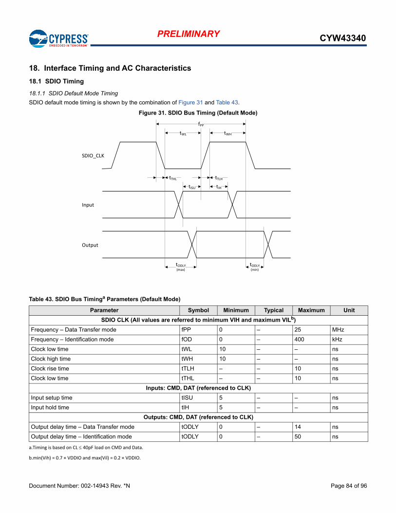
Document Number: 002-14943 Rev. *N Page 84 of 96
PRELIMINARY CYW43340
18. Interface Timing and AC Characteristics
18.1 SDIO Timing
18.1.1 SDIO Default Mode Timing
SDIO default mode timing is shown by the combination of Figure 31 and Table 43.
Figure 31. SDIO Bus Timing (Default Mode)
Table 43. SDIO Bus Timinga Parameters (Default Mode)
a.Timing is based on CL 40pF load on CMD and Data.
Parameter Symbol Minimum Typical Maximum Unit
SDIO CLK (All values are referred to minimum VIH and maximum VILb)
b.min(Vih) = 0.7 × VDDIO and max(Vil) = 0.2 × VDDIO.
Frequency – Data Transfer mode fPP 0 – 25 MHz
Frequency – Identification mode fOD 0 – 400 kHz
Clock low time tWL 10 – – ns
Clock high time tWH 10 – – ns
Clock rise time tTLH – – 10 ns
Clock low time tTHL – – 10 ns
Inputs: CMD, DAT (referenced to CLK)
Input setup time tISU 5 – – ns
Input hold time tIH 5 – – ns
Outputs: CMD, DAT (referenced to CLK)
Output delay time – Data Transfer mode tODLY 0 – 14 ns
Output delay time – Identification mode tODLY 0 – 50 ns
tWL tWH
fPP
tTHL
tISU
tTLH
tIH
tODLY(max)
tODLY(min)
Input
Output
SDIO_CLK
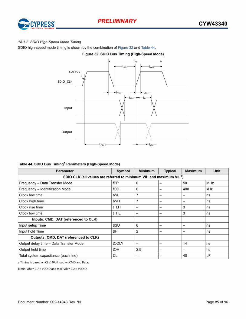
Document Number: 002-14943 Rev. *N Page 85 of 96
PRELIMINARY CYW43340
18.1.2 SDIO High-Speed Mode Timing
SDIO high-speed mode timing is shown by the combination of Figure 32 and Table 44.
Figure 32. SDIO Bus Timing (High-Speed Mode)
Table 44. SDIO Bus Timinga Parameters (High-Speed Mode)
a.Timing is based on CL 40pF load on CMD and Data.
Parameter Symbol Minimum Typical Maximum Unit
SDIO CLK (all values are referred to minimum VIH and maximum VILb)
b.min(Vih) = 0.7 × VDDIO and max(Vil) = 0.2 × VDDIO.
Frequency – Data Transfer Mode fPP 0 – 50 MHz
Frequency – Identification Mode fOD 0 – 400 kHz
Clock low time tWL 7 – – ns
Clock high time tWH 7 – – ns
Clock rise time tTLH – – 3 ns
Clock low time tTHL – – 3 ns
Inputs: CMD, DAT (referenced to CLK)
Input setup Time tISU 6 – – ns
Input hold Time tIH 2 – – ns
Outputs: CMD, DAT (referenced to CLK)
Output delay time – Data Transfer Mode tODLY – – 14 ns
Output hold time tOH 2.5 – – ns
Total system capacitance (each line) CL – – 40 pF
tWL tWH
fPP
tTHL
tISU
tTLH
tIH
tODLY
Input
Output
50% VDD
tOH
SDIO_CLK
Document Number: 002-14943 Rev. *N Page 86 of 96
PRELIMINARY CYW43340
18.2 HSIC Interface Specifications
18.3 JTAG Timing
Table 45. HSIC Timing Parameters
Parameter Symbol Minimum Typical Maximum Unit Comments
HSIC signaling voltage VDD 1.1 1.2 1.3 V –
I/O voltage input low VIL –0.3 – 0.35 × VDD V –
I/O Voltage input high VIH 0.65 × VDD – VDD + 0.3 V –
I/O voltage output low VOL – – 0.25 × VDD V –
I/O voltage output high VOH 0.75 × VDD – – V –
I/O pad drive strength OD 40 – 60 Ω Controlled output impedance driver
I/O weak keepers IL 20 – 70 μA –
I/O input impedance ZI 100 – – kΩ –
Total capacitive loada
a.Total Capacitive Load (CL), includes device Input/Output capacitance, and capacitance of a 50Ω PCB trace with a length of 10 cm.
CL 3 – 14 pF –
Characteristic trace impedance TI 45 50 55 Ω –
Circuit board trace length TL – – 10 cm –
Circuit board trace propagation skewb
b.Maximum propagation delay skew in STROBE or DATA with respect to each other. The trace delay should be matched between STROBE and DATA to ensure
that the signal timing is within specification limits at the receiver.
TS – – 15 ps –
STROBE frequencyc
c.Jitter and duty cycle are not separately specified parameters, they are incorporated into the values in the table above.
FSTROBE 239.988 240 240.012 MHz ± 500 ppm
Slew rate (rise and fall) STROBE and DATAC
Tslew 0.60 × VDD 1.0 1.2 V/ns Averaged from 30% ~ 70% points
Receiver data setup time (with respect to STROBE)c
Ts 300 – – ps Measured at the 50% point
Receiver data hold time (with respect to STROBE)c
Tb 300 – – ps Measured at the 50% point
Table 46. JTAG Timing Characteristics
Signal Name Period OutputMaximum
OutputMinimum Setup Hold
TCK 125 ns – – – –
TDI – – – 20 ns 0 ns
TMS – – – 20 ns 0 ns
TDO – 100 ns 0 ns – –
JTAG_TRST 250 ns – – – –
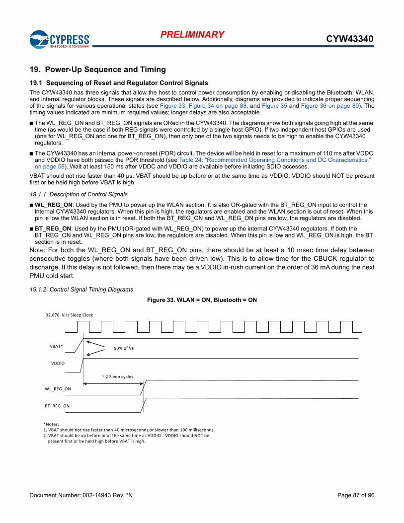
Document Number: 002-14943 Rev. *N Page 87 of 96
PRELIMINARY CYW43340
19. Power-Up Sequence and Timing
19.1 Sequencing of Reset and Regulator Control Signals
The CYW43340 has three signals that allow the host to control power consumption by enabling or disabling the Bluetooth, WLAN,and internal regulator blocks. These signals are described below. Additionally, diagrams are provided to indicate proper sequencingof the signals for various operational states (see Figure 33, Figure 34 on page 88, and Figure 35 and Figure 36 on page 89). Thetiming values indicated are minimum required values; longer delays are also acceptable.
The WL_REG_ON and BT_REG_ON signals are ORed in the CYW43340. The diagrams show both signals going high at the same time (as would be the case if both REG signals were controlled by a single host GPIO). If two independent host GPIOs are used (one for WL_REG_ON and one for BT_REG_ON), then only one of the two signals needs to be high to enable the CYW43340 regulators.
The CYW43340 has an internal power-on reset (POR) circuit. The device will be held in reset for a maximum of 110 ms after VDDC and VDDIO have both passed the POR threshold (see Table 24: “Recommended Operating Conditions and DC Characteristics,” on page 58). Wait at least 150 ms after VDDC and VDDIO are available before initiating SDIO accesses.
VBAT should not rise faster than 40 µs. VBAT should be up before or at the same time as VDDIO. VDDIO should NOT be presentfirst or be held high before VBAT is high.
19.1.1 Description of Control Signals
WL_REG_ON: Used by the PMU to power up the WLAN section. It is also OR-gated with the BT_REG_ON input to control the internal CYW43340 regulators. When this pin is high, the regulators are enabled and the WLAN section is out of reset. When this pin is low the WLAN section is in reset. If both the BT_REG_ON and WL_REG_ON pins are low, the regulators are disabled.
BT_REG_ON: Used by the PMU (OR-gated with WL_REG_ON) to power up the internal CYW43340 regulators. If both the BT_REG_ON and WL_REG_ON pins are low, the regulators are disabled. When this pin is low and WL_REG_ON is high, the BT section is in reset.
Note: For both the WL_REG_ON and BT_REG_ON pins, there should be at least a 10 msec time delay betweenconsecutive toggles (where both signals have been driven low). This is to allow time for the CBUCK regulator todischarge. If this delay is not followed, then there may be a VDDIO in-rush current on the order of 36 mA during the nextPMU cold start.
19.1.2 Control Signal Timing Diagrams
Figure 33. WLAN = ON, Bluetooth = ON
32.678 kHz Sleep Clock
VBAT*
VDDIO
WL_REG_ON
BT_REG_ON
90% of VH
~ 2 Sleep cycles
*Notes:1. VBAT should not rise faster than 40 microseconds or slower than 100 milliseconds.2. VBAT should be up before or at the same time as VDDIO . VDDIO should NOT be
present first or be held high before VBAT is high .
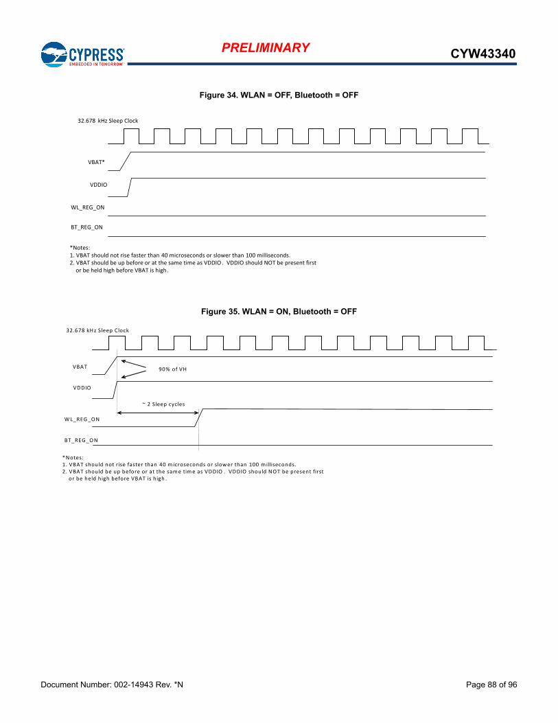
Document Number: 002-14943 Rev. *N Page 88 of 96
PRELIMINARY CYW43340
Figure 34. WLAN = OFF, Bluetooth = OFF
Figure 35. WLAN = ON, Bluetooth = OFF
32.678 kHz Sleep Clock
VBAT*
VDDIO
WL_REG_ON
BT_REG_ON
*Notes:1. VBAT should not rise faster than 40 microseconds or slower than 100 milliseconds.2. VBAT should be up before or at the same time as VDDIO . VDDIO should NOT be present first or be held high before VBAT is high.
32.678 kHz Sleep Clock
VBAT
VDDIO
WL_REG_ON
BT_REG_ON
90% of VH
~ 2 Sleep cycles
*Notes:1. VBAT should not rise faster than 40 m icroseconds or slower than 100 m illiseconds.2. VBAT should be up before or at the same time as VDDIO . VDDIO should NOT be present first
or be held high before VBAT is high .
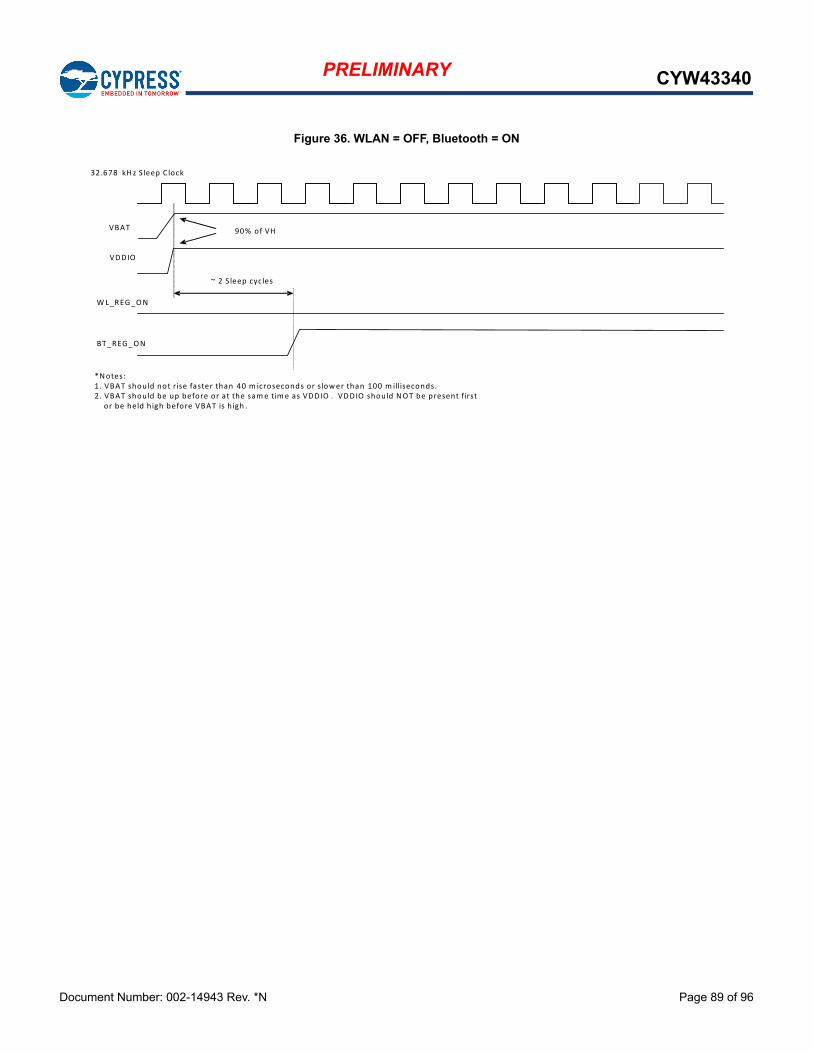
Document Number: 002-14943 Rev. *N Page 89 of 96
PRELIMINARY CYW43340
Figure 36. WLAN = OFF, Bluetooth = ON
32.678 kHz S leep Clock
VBAT
VDDIO
WL_REG_ON
BT_REG_ON
90% of VH
~ 2 S leep cycles
*Notes:1. VBAT should not rise faster than 40 m icroseconds or slower than 100 m illiseconds.2. VBAT should be up before or at the same time as VDDIO . VDDIO should NOT be present first
or be held h igh before VBAT is h igh .
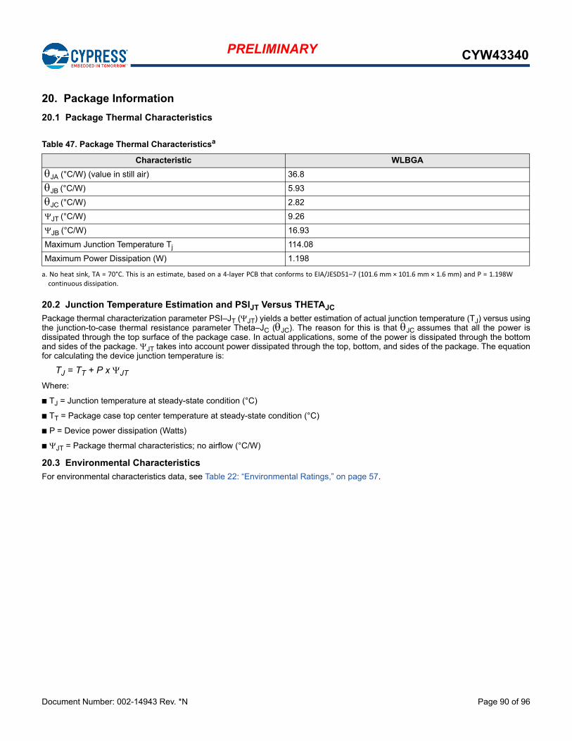
Document Number: 002-14943 Rev. *N Page 90 of 96
PRELIMINARY CYW43340
20. Package Information
20.1 Package Thermal Characteristics
20.2 Junction Temperature Estimation and PSIJT Versus THETAJC
Package thermal characterization parameter PSI–JT (JT) yields a better estimation of actual junction temperature (TJ) versus usingthe junction-to-case thermal resistance parameter Theta–JC (JC). The reason for this is that JC assumes that all the power isdissipated through the top surface of the package case. In actual applications, some of the power is dissipated through the bottomand sides of the package. JT takes into account power dissipated through the top, bottom, and sides of the package. The equationfor calculating the device junction temperature is:
TJ = TT + P x JT
Where:
TJ = Junction temperature at steady-state condition (°C)
TT = Package case top center temperature at steady-state condition (°C)
P = Device power dissipation (Watts)
JT = Package thermal characteristics; no airflow (°C/W)
20.3 Environmental Characteristics
For environmental characteristics data, see Table 22: “Environmental Ratings,” on page 57.
Table 47. Package Thermal Characteristicsa
a. No heat sink, TA = 70°C. This is an estimate, based on a 4-layer PCB that conforms to EIA/JESD51–7 (101.6 mm × 101.6 mm × 1.6 mm) and P = 1.198Wcontinuous dissipation.
Characteristic WLBGA
JA (°C/W) (value in still air) 36.8
JB (°C/W) 5.93
JC (°C/W) 2.82
JT (°C/W) 9.26
JB (°C/W) 16.93
Maximum Junction Temperature Tj 114.08
Maximum Power Dissipation (W) 1.198
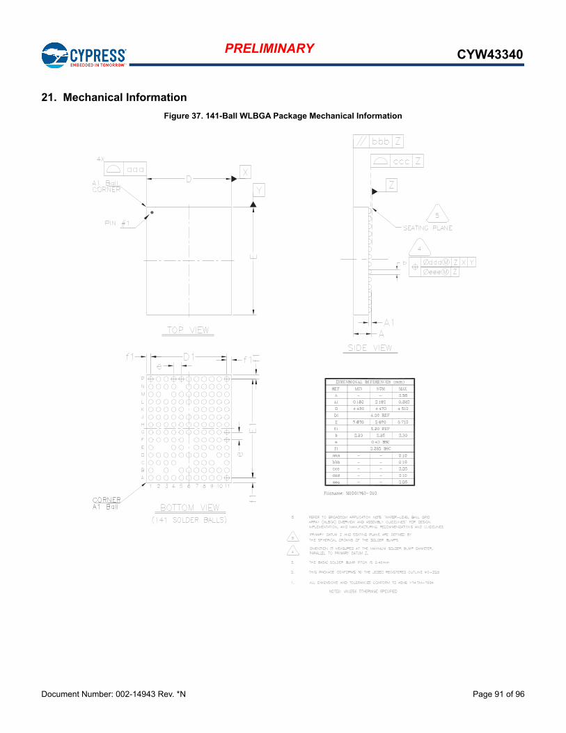
Document Number: 002-14943 Rev. *N Page 91 of 96
PRELIMINARY CYW43340
21. Mechanical Information
Figure 37. 141-Ball WLBGA Package Mechanical Information
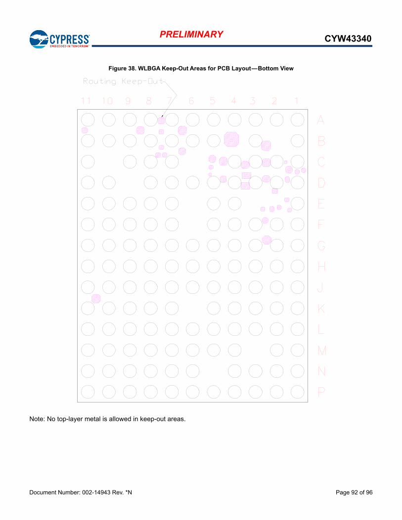
Document Number: 002-14943 Rev. *N Page 92 of 96
PRELIMINARY CYW43340
Figure 38. WLBGA Keep-Out Areas for PCB Layout—Bottom View
Note: No top-layer metal is allowed in keep-out areas.
Document Number: 002-14943 Rev. *N Page 93 of 96
PRELIMINARY CYW43340
22. Ordering Information
23. Additional Information
23.1 Acronyms and Abbreviations
In most cases, acronyms and abbreviations are defined on first use.
For a comprehensive list of acronyms and other terms used in Cypress documents, go to http://www.cypress.com/glossary.
23.2 IoT Resources
Cypress provides a wealth of data at http://www.cypress.com/internet-things-iot to help you to select the right IoT device for your design, and quickly and effectively integrate the device into your design. Cypress provides customer access to a wide range of information, including technical documentation, schematic diagrams, product bill of materials, PCB layout information, and software updates. Customers can acquire technical documentation and software from the Cypress Support Community website (http://community.cypress.com/)
Part Number Package Description Operating Ambi-ent Temperature
CYW43340XKUBG 141 ball WLBGA(5.67 mm × 4.47 mm, 0.4 mm pitch)
Dual-band 2.4 GHz and 5 GHz WLAN + BT 5.0
–30°C to +85°C
CYW43340HKUBG 141 ball WLBGA(5.67 mm × 4.47 mm, 0.4 mm pitch)
Dual-band 2.4 GHz and 5 GHz WLAN + BT 5.0 + BSP
–30°C to +85°C
Document Number: 002-14943 Rev. *N Page 94 of 96
PRELIMINARY CYW43340
Document History
Document Title: CYW43340, Single-Chip, Dual-Band (2.4 GHz/5 GHz) IEEE 802.11 a/b/g/n MAC/Baseband/Radio with Inte-grated Bluetooth 5.0Document Number: 002-14943
Revision ECN Submission Date Description of Change
** - 07/09/2012 43340–DS100-R:Initial Release
*A - 12/21/2012 43340–DS101-R:Updated:HCI high-speed UART: H4+ mode no longer supported.General Description on page 1.“IEEE 802.11x Key Features” on page 5: shared Bluetooth and 2.4 GHz WLAN signal path.Figure 11: “Startup Signaling Sequence,” on page 54.“External Coexistence Interface” on page 80.Table 26: “WLBGA and WLCSP Signal Descriptions,” on page 127.Table 27: “WLAN GPIO Functions and Strapping Options (Advance Information),” on page 140.Table 31: “I/O States,” on page 145 .Table 32: “Absolute Maximum Ratings,” on page 149.Table 36: “Bluetooth Receiver RF Specifications,” on page 154.Table 37: “Bluetooth Transmitter RF Specifications,” on page 158.Table 53: “Typical WLAN Power Consumption,” on page 185.Table 54: “Bluetooth and FM Current Consumption,” on page 187.
*B - 04/22/2013 43340–DS102-R:Updated:Figure 1: “Functional Block Diagram,” on page 1.AES feature description on page 5.VBAT voltage range changed from 2.3–4.8V to 2.9–4.8V.Figure 4: “Typical Power Topology,” on page 29.“Link Control Layer” on page 51: substates.Table 33: “Bluetooth Receiver RF Specifications,” on page 131.Figure 52: “WLAN Port Locations (5 GHz),” on page 142.Table 34: “Bluetooth Transmitter RF Specifications,” on page 135: Power control step.Table 36: “BLE RF Specifications,” on page 136: Rx sense.Table 37: “FM Receiver Specifications,” on page 137.Table 39: “WLAN 2.4 GHz Receiver Performance Specifications,” on page 144.Table 40: “WLAN 2.4 GHz Transmitter Performance Specifications,” on page 148.Table 42: “WLAN 5 GHz Transmitter Performance Specifications,” on page 153.Table 50: “Typical WLAN Power Consumption,” on page 162.
*C 08/30/0213 43340–DS103-R:Removed ‘Preliminary’ from the document type.
*D - 12/03/2013 43340–DS104-R:Updated:Proprietary protocols in “Standards Compliance” on page 21.Table 24: “ESD Specifications,” on page 102.Table 33: “WLAN 2.4 GHz Transmitter Performance Specifications,” on page 124.Table 35: “WLAN 5 GHz Transmitter Performance Specifications,” on page 129.
*E - 02/14/2014 43340–DS105-R:Updated:Section 26: “Ordering Information,” on page 194.
*F - 03/04/0214 43340–DS106-R:Figure 38: “141-Bump CYW43340 WLBGA Ball Map (Bottom View),” on page 58 and Table 18: “WLBGA Signal Descriptions,” on page 59: Updated signal names for No Connect, VDDC, VDDIO, VSS, VSSC, and WRF_PA5G_VBAT_GND3P3 pins.
*G - 04/07/2014 43340–DS107-R:Updated:[43341]Figure 48: “NFC Boot-Up Sequence (Secure Patch Download) from Snooze,” on page 117[43341]“NFC Operation Requirement” on page 119Table 28: “WLAN GPIO Functions and Strapping Options (Advance Information),” on page 144Title change (2.5 GHz to 2.4 GHz) for Figure 55 on page 169
*H - 07/07/2014 43340–DS108-R:Updated:Figure 65: “WLBGA Keep-Out Areas for PCB Layout — Bottom View,” on page 177
*I - 01/28/2015 43340–DS109-R:Updated:Table 18: “WLBGA Signal Descriptions,” on page 59
Document Number: 002-14943 Rev. *N Page 95 of 96
PRELIMINARY CYW43340
*J - 09/10/2015 43340–DS110-R:Updated:Table 32: “WLAN 2.4 GHz Receiver Performance Specifications,” on page 85
*K 5529544 11/23/2016 Updated to Cypress template
*L 5675330 03/28/2017 Removed FM and gSPI sections throughout the document.
*M 6257183 07/23/2018 Updated Document Title to read as “CYW43340, Single-Chip, Dual-Band (2.4 GHz/5 GHz) IEEE 802.11 a/b/g/n MAC/Baseband/Radio with Integrated Bluetooth 5.0”.Replaced “Bluetooth 4.0” with “Bluetooth 5.0” in all instances across the document.
*N 7108765 03/24/2021 Removed Cypress Numbering Scheme.Updated Features and WLAN PHY Description.
Document Title: CYW43340, Single-Chip, Dual-Band (2.4 GHz/5 GHz) IEEE 802.11 a/b/g/n MAC/Baseband/Radio with Inte-grated Bluetooth 5.0Document Number: 002-14943
Revision ECN Submission Date Description of Change
Document Number: 002-14943 Rev. *N Revised March 24, 2021 Page 96 of 96
© Cypress Semiconductor Corporation, 2012-2021. This document is the property of Cypress Semiconductor Corporation, and Infineon Technologies company, and its affiliates (“Cypress”). This document, including any software or firmware included or referenced in this document (“Software”), is owned by Cypress under the intellectual property laws and treaties of the United States and other countries worldwide. Cypress reserves all rights under such laws and treaties and does not, except as specifically stated in this paragraph, grant any license under its patents, copyrights, trademarks, or other intellectual property rights. If the Software is not accompanied by a license agreement and you do not otherwise have a written agreement with Cypress governing the use of the Software, then Cypress hereby grants you a personal, non-exclusive, nontransferable license (without the right to sublicense) (1) under its copyright rights in the Software (a) for Software provided in source code form, to modify and reproduce the Software solely for use with Cypress hardware products, only internally within your organization, and (b) to distribute the Software in binary code form externally to end users (either directly or indirectly through resellers and distributors), solely for use on Cypress hardware product units, and (2) under those claims of Cypress’s patents that are infringed by the Software (as provided by Cypress, unmodified) to make, use, distribute, and import the Software solely for use with Cypress hardware products. Any other use, reproduction, modification, translation, or compilation of the Software is prohibited.
TO THE EXTENT PERMITTED BY APPLICABLE LAW, CYPRESS MAKES NO WARRANTY OF ANY KIND, EXPRESS OR IMPLIED, WITH REGARD TO THIS DOCUMENT OR ANY SOFTWARE OR ACCOMPANYING HARDWARE, INCLUDING, BUT NOT LIMITED TO, THE IMPLIED WARRANTIES OF MERCHANTABILITY AND FITNESS FOR A PARTICULAR PURPOSE. No computing device can be absolutely secure. Therefore, despite security measures implemented in Cypress hardware or software products, Cypress shall have no liability arising out of any security breach, such as unauthorized access to or use of a Cypress product. CYPRESS DOES NOT REPRESENT, WARRANT, OR GUARANTEE THAT CYPRESS PRODUCTS, OR SYSTEMS CREATED USING CYPRESS PRODUCTS, WILL BE FREE FROM CORRUPTION, ATTACK, VIRUSES, INTERFERENCE, HACKING, DATA LOSS OR THEFT, OR OTHER SECURITY INTRUSION (collectively, “Security Breach”). Cypress disclaims any liability relating to any Security Breach, and you shall and hereby do release Cypress from any claim, damage, or other liability arising from any Security Breach. In addition, the products described in these materials may contain design defects or errors known as errata which may cause the product to deviate from published specifications. To the extent permitted by applicable law, Cypress reserves the right to make changes to this document without further notice. Cypress does not assume any liability arising out of the application or use of any product or circuit described in this document. Any information provided in this document, including any sample design information or programming code, is provided only for reference purposes. It is the responsibility of the user of this document to properly design, program, and test the functionality and safety of any application made of this information and any resulting product. “High-Risk Device” means any device or system whose failure could cause personal injury, death, or property damage. Examples of High-Risk Devices are weapons, nuclear installations, surgical implants, and other medical devices. “Critical Component” means any component of a High-Risk Device whose failure to perform can be reasonably expected to cause, directly or indirectly, the failure of the High-Risk Device, or to affect its safety or effectiveness. Cypress is not liable, in whole or in part, and you shall and hereby do release Cypress from any claim, damage, or other liability arising from any use of a Cypress product as a Critical Component in a High-Risk Device. You shall indemnify and hold Cypress, including its affiliates, and its directors, officers, employees, agents, distributors, and assigns harmless from and against all claims, costs, damages, and expenses, arising out of any claim, including claims for product liability, personal injury or death, or property damage arising from any use of a Cypress product as a Critical Component in a High-Risk Device. Cypress products are not intended or authorized for use as a Critical Component in any High-Risk Device except to the limited extent that (i) Cypress’s published data sheet for the product explicitly states Cypress has qualified the product for use in a specific High-Risk Device, or (ii) Cypress has given you advance written authorization to use the product as a Critical Component in the specific High-Risk Device and you have signed a separate indemnification agreement.
Cypress, the Cypress logo, and combinations thereof, WICED, ModusToolBox, PSoC, CapSense, EZ-USB, F-RAM, and Traveo are trademarks or registered trademarks of Cypress or a subsidiaryof Cypress in the United States or in other countries. For a more complete list of Cypress trademarks, visit cypress.com. Other names and brands may be claimed as property of their respective owners.
PRELIMINARY CYW43340
Sales, Solutions, and Legal Information
Worldwide Sales and Design Support
Cypress maintains a worldwide network of offices, solution centers, manufacturer’s representatives, and distributors. To find the office closest to you, visit us at Cypress Locations.
Products
Arm® Cortex® Microcontrollers cypress.com/arm
Automotive cypress.com/automotive
Clocks & Buffers cypress.com/clocks
Interface cypress.com/interface
Internet of Things cypress.com/iot
Memory cypress.com/memory
Microcontrollers cypress.com/mcu
PSoC cypress.com/psoc
Power Management ICs cypress.com/pmic
Touch Sensing cypress.com/touch
USB Controllers cypress.com/usb
Wireless Connectivity cypress.com/wireless
PSoC® Solutions
PSoC 1 | PSoC 3 | PSoC 4 | PSoC 5LP | PSoC 6 MCU
Cypress Developer Community
Community | Projects | Video | Blogs | Training | Components
Technical Support
cypress.com/support
96
Related Documents


