CS 2204 Fall CS 2204 Fall 2005 2005 Experiment 6 Lab 13 Lab 12 Lab 11

CS 2204 Fall 2005 Experiment 6 Lab 13 Lab 12 Lab 11.
Dec 21, 2015
Welcome message from author
This document is posted to help you gain knowledge. Please leave a comment to let me know what you think about it! Share it to your friends and learn new things together.
Transcript
CS 2204 Fall 2005CS 2204 Fall 2005Experiment 6Lab 13
Lab 12
Lab 11
Experiment 6 Lab 13 Lab 12 Lab 11
Page 2CS 2204 Fall 2005
Today’s Xilinx Work We will start developing the Experiment 6
Xilinx project, M4We will start designing Block 6, the Machine
Play Block, of the term project There is one black box, macro, to implement : M4

Experiment 6 Lab 13 Lab 12 Lab 11
Page 3CS 2204 Fall 2005
Today’s Xilinx Work Start developing Block 6 of the Ppm term project
as Experiment 6
Input/Output Devices
Control Unit, Block 1
Play Check Block
Figure 6. Block partitioning of the Ppm term project.
(Block 1)
Block 4
Machine Play BlockBlock 6
Datapath(Data Unit)
(Experiment 6)
Core
means the blockis partially core
Human Play Block
Block 3 Core
Points Calculation
Block, Block 5
(Experiment 5)
Input/
Block,
Block 2
Output
Core
**Core
M1M2M3
M4

Experiment 6 Lab 13 Lab 12 Lab 11
Page 4CS 2204 Fall 2005
Block 6 as the Machine Play Block Plays for the machine player
It determines if it wants to play the random digit If yes, P2SEL and P2sub are determined & P2played = 1
• No more than one of P2SEL can be one at a time If no, it skips : P2skip = 1
P2played and P2skip are not 1 at the same time If both P2played and P2skip are 0, it means the machine
player is thinking Developing Block 6 is determining these seven outputs
Experiment 6 Lab 13 Lab 12 Lab 11
Page 5CS 2204 Fall 2005
Block 6 as the Machine Play Block Plays for the machine player
The goal is to develop an intelligent machine player It gathers information about the current situation Decides how to play
Therefore, Block 6 must have at least two subblocks
Information Gathering Subblock & Decision Making Subblock
However, there are situations where these two subblocks are merged & a new subblock, a Sequencing Subblock is used

Experiment 6 Lab 13 Lab 12 Lab 11
Page 6CS 2204 Fall 2005
Macro M4
Experiment 6 Lab 13 Lab 12 Lab 11
Page 7CS 2204 Fall 2005
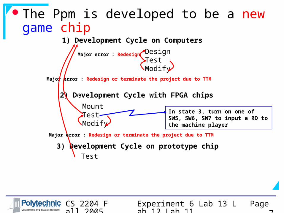
The Ppm is developed to be a new game chip
1) Development Cycle on Computers
DesignTestModify
Major error : Redesign
2) Development Cycle with FPGA chips
MountTestModify
Major error : Redesign or terminate the project due to TTM
3) Development Cycle on prototype chip
Test
Major error : Redesign or terminate the project due to TTM
In state 3, turn on one of SW5, SW6, SW7 to input a RD to the machine player

Experiment 6 Lab 13 Lab 12 Lab 11
Page 8CS 2204 Fall 2005
Designing a New Chip DESIGN
1) Input/Output relationshipa) A simple circuit : get the expression(s)b) A complex circuit : Obtain the operation
table/diagram Then, partition the block based on major operations, design goals and available components
Move on to the Implementation step, (2)
Experiment 6 Lab 13 Lab 12 Lab 11
Page 9CS 2204 Fall 2005
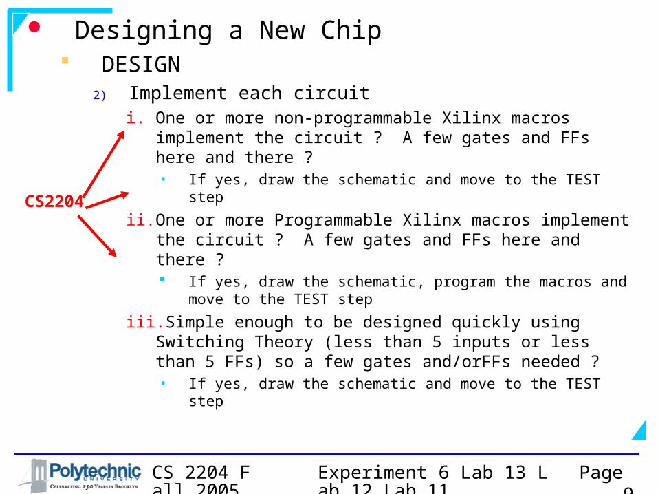
Designing a New Chip DESIGN
2) Implement each circuiti. One or more non-programmable Xilinx macros
implement the circuit ? A few gates and FFs here and there ?• If yes, draw the schematic and move to the TEST step
ii. One or more Programmable Xilinx macros implement the circuit ? A few gates and FFs here and there ? If yes, draw the schematic, program the macros and move
to the TEST step
iii. Simple enough to be designed quickly using Switching Theory (less than 5 inputs or less than 5 FFs) so a few gates and/orFFs needed ?• If yes, draw the schematic and move to the TEST step
CS2204

Experiment 6 Lab 13 Lab 12 Lab 11
Page 10CS 2204 Fall 2005
Designing a New Chip DESIGN
2) Implement each circuitiv. The circuit can be licensed ?
• If yes, borrow it, place it and move to the TEST step
v. If no to all the above questions, go back to step 1 to partition it further
CS2204

Experiment 6 Lab 13 Lab 12 Lab 11
Page 11CS 2204 Fall 2005
Designing a New Chip TEST
Test (sub)blocks separately Functional and timing simulations by applying test
vectors• Pick the right test vectors and the right order of
them Combine (sub)blocks one at a time

Experiment 6 Lab 13 Lab 12 Lab 11
Page 12CS 2204 Fall 2005
Designing a New Chip MODIFY
A simple changeMinimize the circuit after you think your circuit
does not have logic and timing errors After the minimization, test the circuit to make sure
the minimization does not introduce logic and timing errors

Experiment 6 Lab 13 Lab 12 Lab 11
Page 13CS 2204 Fall 2005
CS2204 components Available components for a new chip
Generic componentsLectures, homework, exams
Xilinx componentsLabs
Gates Flip-flops Popular digital circuits Gates Flip-flops Popular digital circuits
ANDORNOTNANDNOR…
DJKTSR…
ADDerComparatorMUXDeMuxDecoderEncoderALUCounterRegister…
ANDORNOTNANDNOR…
DJK
ADDerComparatorMUXDeMuxDecoderEncoderALUCounterRegister…
Lab design
Use Xilinx Design Blocks, XDBs, macros as much as possible
Experiment 6 Lab 13 Lab 12 Lab 11
Page 14CS 2204 Fall 2005
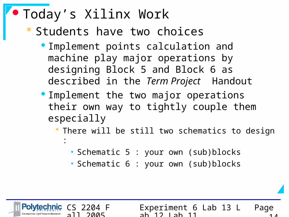
Today’s Xilinx Work Students have two choices
Implement points calculation and machine play major operations by designing Block 5 and Block 6 as described in the Term Project Handout
Implement the two major operations their own way to tightly couple them especially
There will be still two schematics to design :• Schematic 5 : your own (sub)blocks• Schematic 6 : your own (sub)blocks

Experiment 6 Lab 13 Lab 12 Lab 11
Page 15CS 2204 Fall 2005
Today’s Xilinx Work The timetable for the rest of the semester
Students will submit the Experiment 6 project which will include the implementation of the two major operations the way described in the Term Project Handout or their own way
The deadline : Friday, December 9, 2005

Experiment 6 Lab 13 Lab 12 Lab 11
Page 16CS 2204 Fall 2005
Today’s Xilinx Lab WorkComplete implementing Macro M1, M2 and M3
If you are following the Term Project Handout
Start the work on the machine player, M4Determine the playing strategy (intelligence)Partition Block 6 into subblocks and subsubblocksStart implementing the circuits of Block 6
Create an exp6 folderCopy the content of exp5 to exp6
The ppm folder and ppm Xilinx pdf file

Experiment 6 Lab 13 Lab 12 Lab 11
Page 17CS 2204 Fall 2005
Today’s Xilinx Lab Work1. Implementing the machine player, Block 6, M4
i. Read the Playing Rules of the Ppm Game Handoutii. Read the Introduction to Digital Systems and the Ppm
Project Handoutiii. Read the related sections of the Term Project Handoutiv. Decide about the playing strategy of the machine playerv. Decide how to implement the machine playervi. Start developing the schematic
a) Delete M4b) Plan where to place the subblocks on the screenc) Start placing the components

Experiment 6 Lab 13 Lab 12 Lab 11
Page 18CS 2204 Fall 2005
Today’s Xilinx Lab Work2. Implementing the machine player, Block 6, M4
Machine
Player
P2SEL
4
P2played
P2skip
P2sub
.
.
.
•Must generate the seven outputs for correct operation•The Ppm will stay in state 4 when the machine thinks : both P2played and P2skip are zero
•It stays in state 4 at least one Sysclk period•The selection of inputs depends on the strategy and the implementation

Experiment 6 Lab 13 Lab 12 Lab 11
Page 19CS 2204 Fall 2005
Today’s Xilinx Lab Work2. Implementing the machine player, Block 6, M4
Example machine player strategy Play aggressively :
• Always plays (does not skip at all)• Plays on the largest reward points position with an
addition (no subtraction at all)• If two or more positions have the same reward,
selects the rightmost one (can also select randomly, or round robin, etc.)
Experiment 6 Lab 13 Lab 12 Lab 11
Page 20CS 2204 Fall 2005
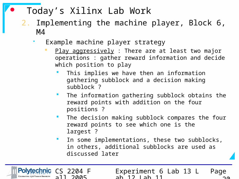
Today’s Xilinx Lab Work2. Implementing the machine player, Block 6, M4
Example machine player strategy Play aggressively : There are at least two major
operations : gather reward information and decide which position to play This implies we have then an information gathering
subblock and a decision making subblock ? The information gathering subblock obtains the
reward points with addition on the four positions ? The decision making subblock compares the four
reward points to see which one is the largest ? In some implementations, these two subblocks, in
others, additional subblocks are used as discussed later

Experiment 6 Lab 13 Lab 12 Lab 11
Page 21CS 2204 Fall 2005
Today’s Xilinx Lab Work2. Implementing the machine player, Block 6, M4
How can we gather the four reward points ? The information gathering subblock has to obtain the adjacency
with addition and then the reward points, i.e. simplified versions of the Adjacency and Reward Calculation Subblocks of Block 5 (That is why tightly coupling Block 5 and Block 6 was suggested earlier) In parallel ? Then four Adjacency circuits and four Reward
Calculation circuits are needed ! Can the limit of the FPGA chip be exceeded ?
In sequence ? Then a sequencing circuit is needed to get the reward points for each position one by one ! A new subblock is needed as the mini sequencer. Can the FPGA chip limit be exceeded ?

Experiment 6 Lab 13 Lab 12 Lab 11
Page 22CS 2204 Fall 2005
Today’s Xilinx Lab Work2. Implementing the machine player, Block 6, M4
How can we compare the four reward points ? In parallel ? Even if the reward points are obtained
sequentially ? Yes ! We have to have three 8-bit comparators and associated control circuits ! Can the limit of the FPGA chip be exceeded ?
In sequence ? Even if the reward points are obtained in parallel ? Yes ! We need to have a sequencing circuit to compare the reward points for each position one by one ! A new subblock is needed as the mini sequencer. Can the FPGA chip limit be exceeded ?

Experiment 6 Lab 13 Lab 12 Lab 11
Page 23CS 2204 Fall 2005
Today’s Xilinx Lab Work2. Implementing the machine player, Block 6, M4
Here are the four choices to implement the strategy : Parallel gathering and parallel compare : can exceed the chip
limit Parallel gathering and sequential compare : store all four reward
points on four registers and then compare them one by one ! A sequencing circuit is needed as the mini sequencer . It does not make sense to do this since the bottom option saves hardware
Sequential gathering and parallel compare : a sequencing circuit is needed to get reward points on four registers one by one. Then, the registers are compared in parallel. It does not make sense to do this since the next option saves hardware
Sequential gathering and sequential compare : a sequencing circuit is needed to get reward points, compare with the previous largest reward and update the reward. The simplest of the four is this one ! The gathering and comparing are combined into one subblock. A second subblock is needed as the mini sequencer

Experiment 6 Lab 13 Lab 12 Lab 11
Page 24CS 2204 Fall 2005
Today’s Xilinx Lab Work2. Implementing the machine player, Block 6, M4
Parallel gather and parallel compare
Determine reward points for four positions and decide where to play
4
Player 2 playson a position
Player 2 spends One Sysclk periods to think
P2SEL = number of the position with the largest reward P2played = 1, P2skip = 0, P2sub = 0
4
Player 2 playson a position
P2sub
Machine
Player
NPDISP 16
P2SEL
4
P2played
P2skip
S4
DISP 16
Sysclk

Experiment 6 Lab 13 Lab 12 Lab 11
Page 25CS 2204 Fall 2005
Today’s Xilinx Lab Work2. Implementing the machine player, Block 6, M4
Parallel gather and parallel compare
•Always plays on a position : it does not skip•Plays on the position with the largest reward by doing an addition : it does not subtract•If two or more positions have the same reward, plays on the rightmost position
Gather
Four
Reward
Points
NPDISP16
8 P0RWD
8 P1RWD
8 P2RWD
8 P3RWD
Compare
and
Select
One
P2SEL
4
P2played
P2skip
P2sub
S4
DISP16
Sysclk

Experiment 6 Lab 13 Lab 12 Lab 11
Page 26CS 2204 Fall 2005
Today’s Xilinx Lab Work2. Implementing the machine player, Block 6, M4
Parallel gather and parallel compare
Position 0Reward Determination
NPDISP4
DISP12
8
P0RWD
Position 1Reward Determination
8
P1RWD
Position 2Reward Determination
8
P2RWD
Position 3Reward Determination
8
Compare & Select One
Compare & Select One
Compareand
SelectOne
P3RWD
8
PXRWD
2
PXNUM
8
PYRWD
2
PYNUM
P2SEL
4
P2played
P2skip
P2sub
NPDISP 4
DISP12
NPDISP4
DISP12
NPDISP4
DISP12
S4Sysclk

Experiment 6 Lab 13 Lab 12 Lab 11
Page 27CS 2204 Fall 2005
Today’s Xilinx Lab Work2.Implementing the machine player, Block 6, M4
Parallel gather and parallel compare
Position 0Adjacency
NPDISP[3-0]4
DISP[15-4]12 8 P0RWD
2 P0NSD
NPDISP[3-0]4
Position 0Reward Calculation
Position 1Adjacency
NPDISP[7-4]4
DISP[15-8 ; 3-0]12 8 P1RWD
2 P1NSD
NPDISP[7-4]4
Position 1Reward Calculation
Position 2Adjacency
NPDISP[11-8]4
DISP[15-12 ; 7-0]12 8 P2RWD
2 P2NSD
NPDISP[11-8]4
Position 2Reward Calculation
Position 3Adjacency
NPDISP[15-12]4
DISP[11-0]12 8 P3RWD
2 P3NSD
NPDISP[15-12]4
Position 3Reward Calculation

Experiment 6 Lab 13 Lab 12 Lab 11
Page 28CS 2204 Fall 2005
Today’s Xilinx Lab Work2.Implementing the machine player, Block 6, M4
Parallel gather and parallel compare8
P0RWD
8P1RWD
Compare
8PXRWD
2PXNUM
Select
8P0RWD
8P1RWD
Select
20
21
Select
Select
8P2RWD
8P3RWD
Compare
8PYRWD
2PYNUM
Select
8P2RWD
8P3RWD
Select
22
23
Select
Select

Experiment 6 Lab 13 Lab 12 Lab 11
Page 29CS 2204 Fall 2005
Today’s Xilinx Lab Work2.Implementing the machine player, Block 6, M4
Parallel gather and parallel compare
S4
R0
R1
2-to
-4 D
ecod
erA0
A1
E
D0
D1
D2
D3
CompareResult &
Select
P2SEL0
P2SEL1
P2SEL2
P2SEL3
P2playedS4
P2skip0
P2sub0
8PXRWD
2PXNUM
8PYRWD
2PYNUM
S4 4-b
it r
egis
ter
CE
C
Q0
Q1
Q2
Q3
Sysclk
I0
I1
I2
I3

Experiment 6 Lab 13 Lab 12 Lab 11
Page 30CS 2204 Fall 2005
Today’s Xilinx Lab Work2.Implementing the machine player, Block 6, M4
Parallel gather and parallel compare
Sysclk
S4
S5
R1,R0
P2SEL 0010
Player 2 plays RD : 1Sysclk period
P2played
S6
S1

Experiment 6 Lab 13 Lab 12 Lab 11
Page 31CS 2204 Fall 2005
Today’s Xilinx Lab Work2. Implementing the machine player, Block 6, M4
Sequential gather and Sequential compare An operation diagram is needed
Player 2 spends FIVE Sysclk periods to think
Machine
Player
RWD
8 P2SEL
4
P2played
P2skip
P2sub
S4
S1
Sysclk
Determine position 0 reward & record the position number
Determine position 1 reward, compare with position 0, keep it if it is larger & record the position number
Determine position 2 reward , compare with the previous, keep it if it is larger & record the position number
Determine Position 3 Reward , compare with the previous, keep it if it is larger, record the position number
0
1
2
3
4
Player 2 playson a position
Based on the stored information select the position to play4
Experiment 6 Lab 13 Lab 12 Lab 11
Page 32CS 2204 Fall 2005
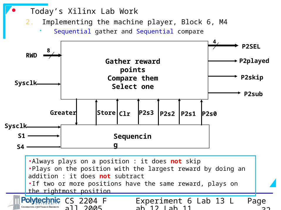
Today’s Xilinx Lab Work2. Implementing the machine player, Block 6, M4
Sequential gather and Sequential compare
Gather reward pointsCompare them
Select one
RWD8
S4
SequencingS1
Sysclk
P2SEL4
P2played
P2skip
P2sub
P2s2 P2s1ClrStoreGreater P2s0P2s3
•Always plays on a position : it does not skip•Plays on the position with the largest reward by doing an addition : it does not subtract•If two or more positions have the same reward, plays on the rightmost position
Sysclk

Experiment 6 Lab 13 Lab 12 Lab 11
Page 33CS 2204 Fall 2005
Today’s Xilinx Lab Work2. Implementing the machine player, Block 6, M4
Sequential gather and Sequential compare
P2SEL = 0001, P2played = 0, P2skip = 0, P2sub = 0Store RWD as the largestStore position number 0
P2SEL = 0010, P2played = 0, P2skip = 0, P2sub = 0Compare RWD with stored position 0 RWD
Store RWD if it is larger & store position number 1
P2SEL = 0100 , P2played = 0, P2skip = 0, P2sub = 0Compare RWD with the with previous largest
Store RWD if it is larger and store position number 2
P2SEL = 1000 , P2played = 0, P2skip = 0, P2sub = 0Compare RWD with the with previous largest
Store RWD if it is larger and store position number 3
0
1
2
3
P2SEL = number of the position with the largest rewardP2played = 1, P2skip = 0, P2sub = 0
4
•Always plays on a position : it does not skip
•Plays on the position with the largest reward by doing an addition : it does not subtract
•If two or more positions have the same reward, plays on the rightmost position

Experiment 6 Lab 13 Lab 12 Lab 11
Page 34CS 2204 Fall 2005
Today’s Xilinx Lab Work2. Implementing the machine player, Block 6, M4
Sequential gather and Sequential compare The Sequencing Subblock
3-b
it u
p c
oun
ter
CE
C
CLR
Q0
Q1
Q2P2skip
P2played
S4
Sysclk
S1
P2streg0
P2streg1
P2streg2
S1
Clr Store
2-to
-4 D
ecod
er
A0
A1
E1
D0
D1
D2
D3
P2s0 P2s1 P2s2 P2s3
P2streg2
Greater
E0
S4
P2streg
S4

Experiment 6 Lab 13 Lab 12 Lab 11
Page 35CS 2204 Fall 2005
Today’s Xilinx Lab Work2.Implementing the machine player, Block 6, M4
Sequential gather and Sequential compare
8-bitComparator
8RWD
8LRGRWD
A
B
A>BGt
8-bitRegister
8RWD
Store
D
CE
Sysclk C
CLR
Clr
8LRGRWD
Q
P2s0Gt
Greater
4-bitRegister
Store CE
Sysclk C
CLR
P2s0D0
P2s1D1
P2s2D2
P2s3D3
POS0Q0
POS1Q1
POS2Q2
POS3Q3
Clr

Experiment 6 Lab 13 Lab 12 Lab 11
Page 36CS 2204 Fall 2005
Today’s Xilinx Lab Work2.Implementing the machine player, Block 6, M4
Sequential gather and Sequential compare
P2SEL0POS0
POS1Compare
Result
P2s0
P2SEL1P2s1
P2SEL2P2s2
P2SEL3P2s3
P2played
S4
P2skip0
P2sub0
P2streg2
POS2
POS3
P2streg2

Experiment 6 Lab 13 Lab 12 Lab 11
Page 37CS 2204 Fall 2005
Today’s Xilinx Lab Work2. Implementing the machine player, Block 6, M4
Sequential gather and Sequential compareSysclk
S4
S5
P2s0
P2s1
P2s2
P2s3
P2streg2
RWD
Greater
Store
LRGRWD
P2SEL 0001 0010 0100 1000 0010
Player 2 thinks and plays RD : 5 Sysclk periods
Position 1 Reward
Position 1 Reward
P2played

Experiment 6 Lab 13 Lab 12 Lab 11
Page 38CS 2204 Fall 2005
Today’s Xilinx Lab Work2. Implementing the machine player, Block 6, M4
Non-intelligent machine player strategies (there are many)1. Play in a fixed way : always play on the rightmost
position which does not have a display overflow. If all positions result in display overflows, skip
2. Play randomly : when it is time to play, stop a freely running 2-bit counter and play on that position
3. Play in a round robin fashion : every time it is the turn, increment a 2-bit counter and play on that position
4. Play on the first 1-adjacency position from right to left

Experiment 6 Lab 13 Lab 12 Lab 11
Page 39CS 2204 Fall 2005
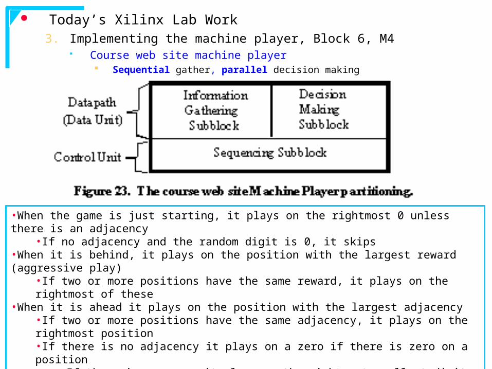
Today’s Xilinx Lab Work3. Implementing the machine player, Block 6, M4
Course web site machine player Machine player strategy
Play for now and future : Play differently for different game situations to eventually win the game It gathers substantial amount of information about the
game and then decides how to play It has an information gathering subblock and an decision
making subblock It gathers the information sequentially and so it has a
sequencing subblock

Experiment 6 Lab 13 Lab 12 Lab 11
Page 40CS 2204 Fall 2005
Today’s Xilinx Lab Work3. Implementing the machine player, Block 6, M4
Course web site machine player Machine player strategy

Experiment 6 Lab 13 Lab 12 Lab 11
Page 41CS 2204 Fall 2005
Today’s Xilinx Lab Work3. Implementing the machine player, Block 6, M4
Course web site machine player Sequential gather, parallel decision making
An operation diagram is needed
Experiment 6 Lab 13 Lab 12 Lab 11
Page 42CS 2204 Fall 2005
Today’s Xilinx Lab Work3. Implementing the machine player, Block 6, M4
Course web site machine player Sequential gather, parallel decision making
•When the game is just starting, it plays on the rightmost 0 unless there is an adjacency•If no adjacency and the random digit is 0, it skips
•When it is behind, it plays on the position with the largest reward (aggressive play)•If two or more positions have the same reward, it plays on the rightmost of these
•When it is ahead it plays on the position with the largest adjacency•If two or more positions have the same adjacency, it plays on the rightmost position•If there is no adjacency it plays on a zero if there is zero on a position
•If there is no zero, it plays on the rightmost smallest digit if there are currently no adjacencies•If there are currently adjacencies, it skips

Experiment 6 Lab 13 Lab 12 Lab 11
Page 43CS 2204 Fall 2005
Today’s Xilinx Lab Work3. Implementing the machine player, Block 6, M4
Course web site machine player sequential gather, parallel decision making
Major portion of the Sequencing Subblock
Figure 25. The counter decoder combination circuit of the Sequencing Subblock.

Experiment 6 Lab 13 Lab 12 Lab 11
Page 44CS 2204 Fall 2005
Today’s Xilinx Lab Work Course web site machine player implementation

Experiment 6 Lab 13 Lab 12 Lab 11
Page 45CS 2204 Fall 2005
Today’s Xilinx Lab Work4. Implementing the machine player, Block 6, M4
Steps to design the machine player1. Determine the strategy and draw a flowchart if necessary2. Decide about the parallel/sequential implementation
issue3. Determine the inputs and draw the black box view4. If sequential operations, determine the operation
diagram5. Partition Block 6 based on the operation diagram6. If sequential operations, implement the sequencing
subblock first

Experiment 6 Lab 13 Lab 12 Lab 11
Page 46CS 2204 Fall 2005
Today’s Xilinx Lab Work4. Implementing the machine player, Block 6, M4
Steps to complete the machine playerAfter drawing the schematics, simulating circuits separately and testing them on the FPGA board1) Label the components, label the subblocks and
subsubblocks2) Beautify it3) Simulate it again4) Do a Xilinx IMPLEMENTATION again 5) Download again to make sure the project is working6) Compare your project with the Experiment 6 Check List
Handout7) Fill out a Project 6 Check List Handout and then signal to a
TA to submit your project8) Your project will be copied to a zip disk by the TA9) Once copied, open the project on the zip disk and download
to the FPGA board to make sure it is copied correctly10) Print schematics 4, 5 and 6 to prepare for the final exam

Experiment 6 Lab 13 Lab 12 Lab 11
Page 47CS 2204 Fall 2005
Today’s Xilinx Lab Work4. Implementing the machine player, Block 6, M4
Printing schematics1) Double click on the Printer227 icon on your desktop and
wait about a minute to allow it to affect the printing option
2) Zoom into an area of the schematic to print the area3) Select File -> Print on the schematic window4) Change the option to Current View Only on the Print
window5) Click on Setup on the Print Window6) Change the printer to HP Printer 8150 in Room 2277) Click on Options to select Landscape printing if necessary8) Click OK as many times as needed to print the page9) Print one copy of each area and then make copies of
the printed schematics for your partners
Experiment 6 Lab 13 Lab 12 Lab 11
Page 48CS 2204 Fall 2005
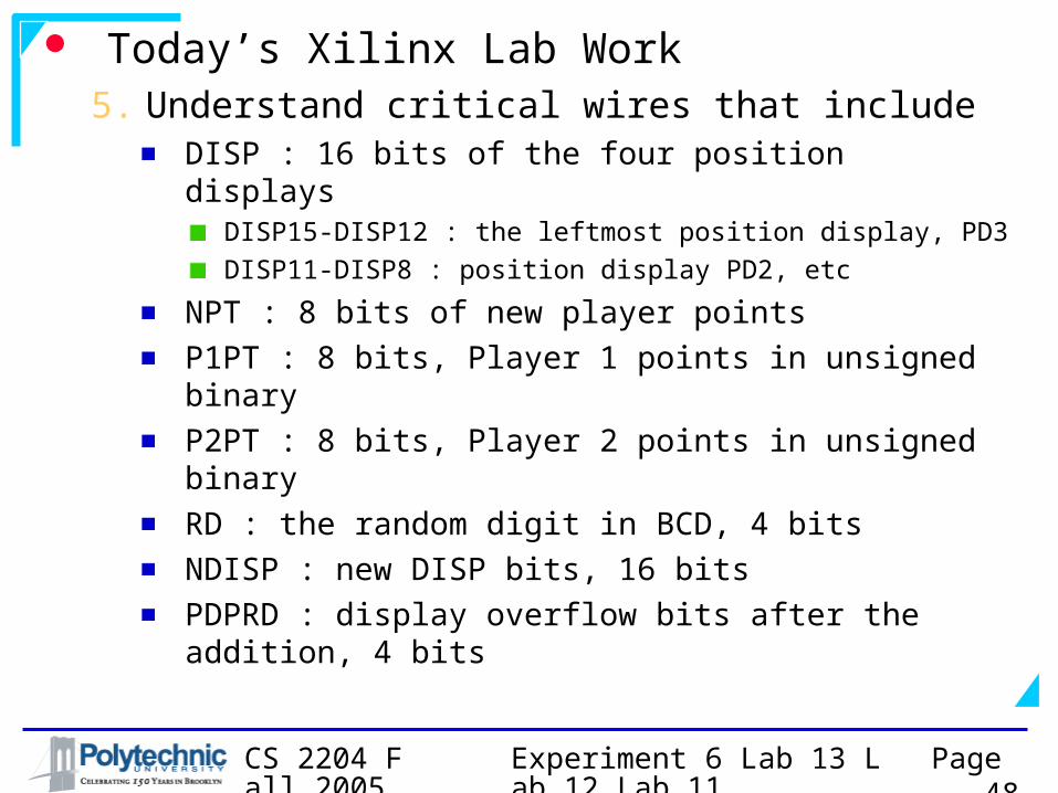
Today’s Xilinx Lab Work5. Understand critical wires that include
DISP : 16 bits of the four position displaysDISP15-DISP12 : the leftmost position display, PD3DISP11-DISP8 : position display PD2, etc
NPT : 8 bits of new player pointsP1PT : 8 bits, Player 1 points in unsigned binaryP2PT : 8 bits, Player 2 points in unsigned binaryRD : the random digit in BCD, 4 bitsNDISP : new DISP bits, 16 bitsPDPRD : display overflow bits after the addition, 4 bits

Experiment 6 Lab 13 Lab 12 Lab 11
Page 49CS 2204 Fall 2005
Today’s Xilinx Lab Work5. Understand the subblocks and critical
wires that include PDMRD : display underflow bits after the subtraction, 4 bitsBRWD : basic reward, the digit played and minimum points earnedEQ : the equality of the position to the digit playedNSD : 2 bits, the number of similar digits, i.e. the adjacency information of the position playedRWD : 8 bits, the reward points earned by the play in Unsigned Binary

Experiment 6 Lab 13 Lab 12 Lab 11
Page 50CS 2204 Fall 2005
Today’s Xilinx Lab Work5. Understand the subblocks and critical
wires that includeBrwdeqz : BRWD is zero when it is 1P1SEL : 4 bits, the position played by the human playerP2SEL : 4 bits, the position played by the machine playerPSEL : 4 bits, position Select bits of current playerENCPSEL : 2 bits, the number of the position played
Experiment 6 Lab 13 Lab 12 Lab 11
Page 51CS 2204 Fall 2005
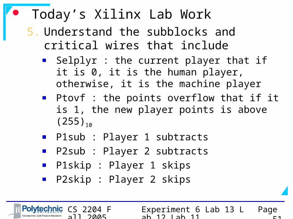
Today’s Xilinx Lab Work5. Understand the subblocks and critical
wires that includeSelplyr : the current player that if it is 0, it is the human player, otherwise, it is the machine playerPtovf : the points overflow that if it is 1, the new player points is above (255)10
P1sub : Player 1 subtractsP2sub : Player 2 subtractsP1skip : Player 1 skipsP2skip : Player 2 skips

Experiment 6 Lab 13 Lab 12 Lab 11
Page 52CS 2204 Fall 2005
Today’s Xilinx Lab Work5. Understand the subblocks and critical
wires that includeP1played : Player 1 playedP2played : Player 2 playedClear : clear FFs, registers, counters, etc. during resetStp1pt : store Player 1 pointsStp2pt : store Player 2 pointsSysclk : system clock of the operation diagram at 6 Hz

Experiment 6 Lab 13 Lab 12 Lab 11
Page 53CS 2204 Fall 2005
Today’s Xilinx Lab Work5.Understand the subblocks and critical
wires that includeNPDISP : 16 bits, display digits plus RDNMDISP : 16 bits, display digits minus RDS1 : State 1. When it is 1, the Ppm is in state 1S4 : State 4. When it is 1, the Ppm is in state 4

Experiment 6 Lab 13 Lab 12 Lab 11
Page 54CS 2204 Fall 2005
The following Xilinx actions and concepts are frequently applied/used Functional simulations of single wires and
buses via the SC Probes toolThe concept of High Impedance (Hi-Z) value
besides the 0 and 1 valuesSeparate inputs from outputs with a blank row
Buffers to rename wires
Experiment 6 Lab 13 Lab 12 Lab 11
Page 55CS 2204 Fall 2005
The following Xilinx actions and concepts are frequently applied/used Copying and pasting schematics via ctrl-c
and ctrl-v Beautifying the schematic for
documentation purposesRotating components via ctrl-r and ctrl-lWires cannot be rotated !
Refreshing screen via F10

Experiment 6 Lab 13 Lab 12 Lab 11
Page 56CS 2204 Fall 2005
The following Xilinx actions and concepts are frequently applied/used Xilinx macros, Hierarchy Push and Pop and the
macro internal structure Gate networks vs Xilinx Design Blocks VCC and GND Knowing that the implementation data is
appended to the end of the Implementation Log file
Clearing the Implementation data from time to time
Knowing that the implementation options must be reentered after clearing the implementation data

Experiment 6 Lab 13 Lab 12 Lab 11
Page 57CS 2204 Fall 2005
The following Xilinx actions and concepts are frequently applied/used Labeling wires and components
Wire names follow application and block partitioning naming requirements
Except for wires that are connected IBUFs, OBUFs, IPADs and OPADs
Compnent names start with a U Except if it is a BUF, IBUF, OBUF, IPAD or OPAD
The Xilinx component library, to look for specific components, checking component properties, features
Experiment 6 Lab 13 Lab 12 Lab 11
Page 58CS 2204 Fall 2005
The following Xilinx actions and concepts are frequently applied/used Searching for wires and components via
SC Query/FindSearching in the schematic for
wires/components specified in the Implementation Log File
Writing Comments and drawing lines and rectangles on the schematic for documentation purpose via Graphics toolbox
Understanding No Load, No Driver and Multiple Driver warnings and errors

Experiment 6 Lab 13 Lab 12 Lab 11
Page 59CS 2204 Fall 2005
The following Xilinx actions and concepts are frequently applied/used Drawing buses by using Draw Buses
buttonPpm buses are type NoneWires of a bus have names the same as the
bus name and indices starting at 0 and up to the number of bus wires minus 1
Bus NPT has 8 wires : NPT7, NPT6, NPT5,…, NPT1, NPT0

Experiment 6 Lab 13 Lab 12 Lab 11
Page 60CS 2204 Fall 2005
QUESTIONS ?
Related Documents