Optimization of the solar cell conversion power by effective front contact design Electrical and Computer Engineering Department Of Iowa State University Authors: Mouhamadou Diallo Antjuan Buffett Nicholas Rodriguez Professor: Dr. Vikram Dalal

Welcome message from author
This document is posted to help you gain knowledge. Please leave a comment to let me know what you think about it! Share it to your friends and learn new things together.
Transcript
Optimization of the solar cell
conversion power by effective
front contact design
Electrical and Computer Engineering Department
Of
Iowa State University
Authors:
Mouhamadou Diallo
Antjuan Buffett
Nicholas Rodriguez
Professor: Dr. Vikram Dalal
Table of Contents
Abstract………………………………………,,,……………p03
Introduction to Solar Cells
Introduction to Solar Energy………………………………....p04
P-N Junctions………………………………………………...p04
Solar Absorption Process……………………………….........p05
Design Details
1. Specifications……………………………………….......p06
2. Methodology…………………………………………... p06
3. Resistive losses on the emitter layer……………………p08
4. Resistive losses in the grid lines………………………..p09
5. Resistive losses in the busbars………………………….p10
6. Shadowing losses of the fingers and busbars………..….p11
7. Optimization………………………………...………….p11
8. Results……………………………………………….….p13
Screen Print Manufacturing
General Overview of the Screen-printing process…………...p14
Project specifications and contact design ink………………..p15
Screen-printing machine description………………………...p15
Processing conditions and parameters……………………….p16
Conclusion………………...………………………...……....p18
References………...………………………………….……...p19

Abstract
The following paper discusses the basic background information and physical structures behind
solar cells as well as completes a design of a specific solar cell with given specifications. The
background information will consist of an introduction to solar energy, p-n junctions, and the
solar cell absorption process. A description of our solar cell design will include our precise
calculations of all losses that we will encounter, go through the optimization process and give a
summary of how the design was chosen. The screen printing manufacturing process and
specifications will be explained and will be using Dupont Solamet PV17A ink. In conclusion we
will explain how the design meets the efficiency requirements and what improvements and
struggles influenced our final decision.
Introduction to Solar Energy
Solar energy, in many different forms, is the source for mostly all energies that we use in
the world today. Fossil fuels are made from dead organisms which have stored solar energy from
millions of years ago. Biomass is derived from living organisms which have taken in solar
energy and can be used to create heat or biofuel. Dams paired with the evaporation process,
completed by the sun, is harnessed as hydropower as well as the sun’s heat mixed with the
atmosphere and the earth’s rotation creates the wind we need for wind energy. Lastly
photovoltaic devices have become the new age way of converting solar radiation directly into
electricity with the use of photovoltaic semiconductors. Solar cells don’t have pollution from
plants, moving parts which wear out, or use slowly or non-renewable material. This makes solar
cells a lot more desirable than other methods of energy harnessing due to their reliability,
longevity and efficiency.
In order for us to understand more about solar energy and the photovoltaic process we
first have a better understanding of sunlight. Sunlight is a lot more than the visable light of
everyday, it is actually in the form of electromagnetic radiation with different ranges of
wavelengths on the electromagnetic spectrum. As sunlight makes its way through the
atmosphere half of the radiation is reflected back into space and the other half that makes it
through reacts with air molecules scattering the light and dispersing its harmful rays. From the
spectrum the sunlights wavelengths range from 100nm (ultraviolet) to 1,000,000nm (infrared),
with visable light ranging from 380 nm to 750nm. The rough percentage of light that is produces
from each spectrum is 47% infrared, 46% ultraviolet, and the remaining 7% is given off as
visable light. In our case, for photovoltaic solar cells, only wavelengths of from approximately
380nm to 750nm (Visable Light) will be absorbed and used to create electricity.
P-N Junctions
There are many different materials and ways to make solar cells and convert solar energy
into usable power but the most commonly used practices of today consist of p-n junctions made
from semiconductor materials. P-N junctions are made by combining both n-type and p-type
semiconductor materials together. The n-type material has extra electrons near the top of its band
gap which makes them easily excited to the conduction band. While on the other side the p-type
materials have extra holes near the bottom of the band gap which allow excitation of valence
band electrons to fill these holes, leaving mobile holes in the valence band. P-n junctions are

made when these two materials are joined together; the electrons diffuse from the n-type side to
the p-type side and through diffusion, the holes move from the p-type to the n-type side [1].
When the electrons and holes switch sides in this manner they create positive ions on the n-side
and negative ions on the p-side, and are fixed in the crystal lattice and cannot move. From this an
electric field is made creating a depletion region which discontinues any further electron
movement [1]. The electric field depletes the region free carrier electrons by swiping them away,
which causes a build in potential voltage to form at the junction.
Figure 1 P-N Junction
Solar Absorbtion Process
A solar cell operates by converting the photons from sunlight that are absorbed, and are
not reflected, into a current and a voltage to generate electric power. For this to happen the
material, such as silicon, of the semiconductor must absorb energy from the photon and this
energy will create a current and electric field from freed electrons and newly created holes. This
will then cause electrons to rise to a higher energy state and from this higher energy state the
electron will then move to an external circuit where it transfers its energy and then returns back
to the lower energy state of the semiconductor material. This process is continuously repeated by
the constant absorption of photons and movement of free electrons. It is required that solar cells
be arranged into an array, to make panels, to capture enough of the suns photons so that it will be
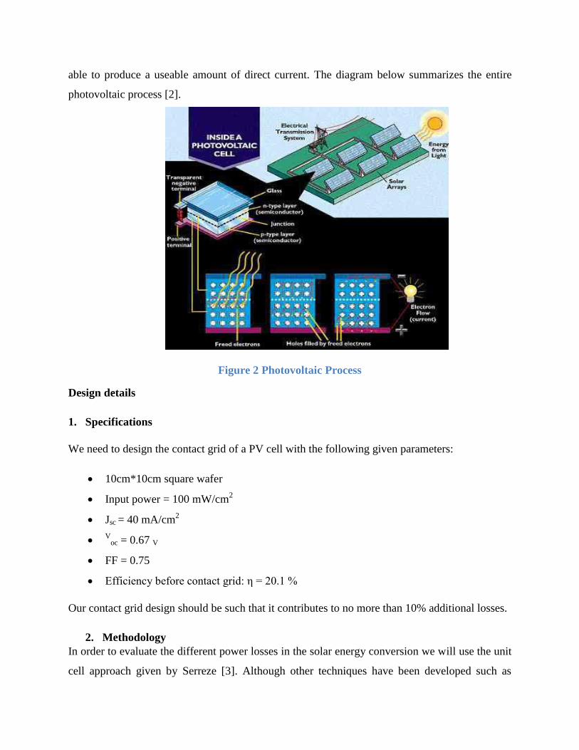
able to produce a useable amount of direct current. The diagram below summarizes the entire
photovoltaic process [2].
Figure 2 Photovoltaic Process
Design details
1. Specifications
We need to design the contact grid of a PV cell with the following given parameters:
10cm*10cm square wafer
Input power = 100 mW/cm2
Jsc = 40 mA/cm2
Voc = 0.67 V
FF = 0.75
Efficiency before contact grid: η = 20.1 %
Our contact grid design should be such that it contributes to no more than 10% additional losses.
2. Methodology
In order to evaluate the different power losses in the solar energy conversion we will use the unit
cell approach given by Serreze [3]. Although other techniques have been developed such as

“virtual smearing approach” [4] and the “minimum voltage drop” approach [5], the unit cell
approach for contact optimization remains widely used in the current literature and is relatively
easy to simulate. By combining the unit cell approach to a use of fractional power loss we will be
able to effectively simplify the computation of the total power loss by only considering the case
of a single unit cell. The dimensions of the basic unit cell in our PV sample will be 2.5cm*10cm.
Figure 3 H-Grid Design of solar cell contacts
By optimizing the design of the contact grids through the busbar width (WB), grid lines width
(WF) and fingers spacing, we will be able to increase the conversion efficiency of the solar cells.
This type of design relies on several assumptions that are worth noting:
The cell is evenly illuminated
The generated current flows homogeneously into the emitter layer and spreads laterally
through the fingers before being collected by the busbars
The fingers and busbars cross sectional areas are rectangular
Fingers are uniform
Optical shadowing comes only from the area covered by the contact grid
Furthermore, since most of our resistive loss equations will involve ratios of the voltage and
current at maximum power (Vmp , Jmp) we will approximate those values with the open-circuit
voltage (Voc) of the cell and the short-circuit current (Jsc). This approximation will not affect the
reliability of our findings as the two ratios are equal [6]:
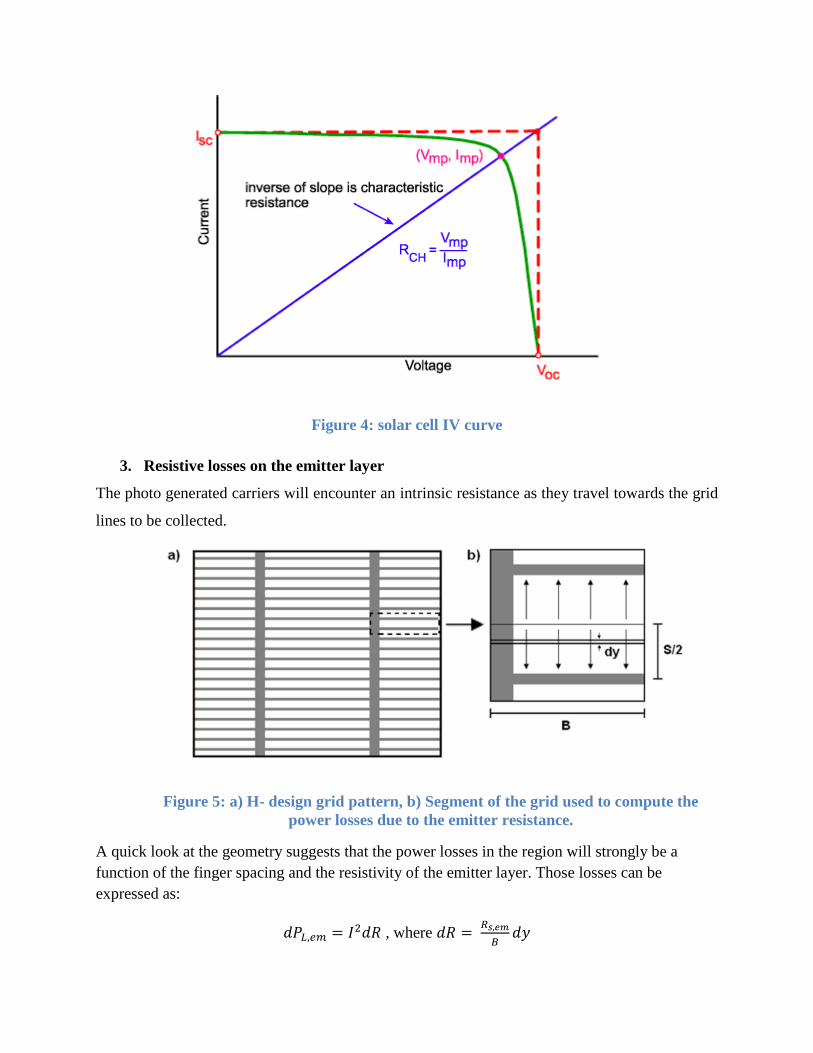
Figure 4: solar cell IV curve
3. Resistive losses on the emitter layer
The photo generated carriers will encounter an intrinsic resistance as they travel towards the grid
lines to be collected.
Figure 5: a) H- design grid pattern, b) Segment of the grid used to compute the
power losses due to the emitter resistance.
A quick look at the geometry suggests that the power losses in the region will strongly be a
function of the finger spacing and the resistivity of the emitter layer. Those losses can be
expressed as:
, where
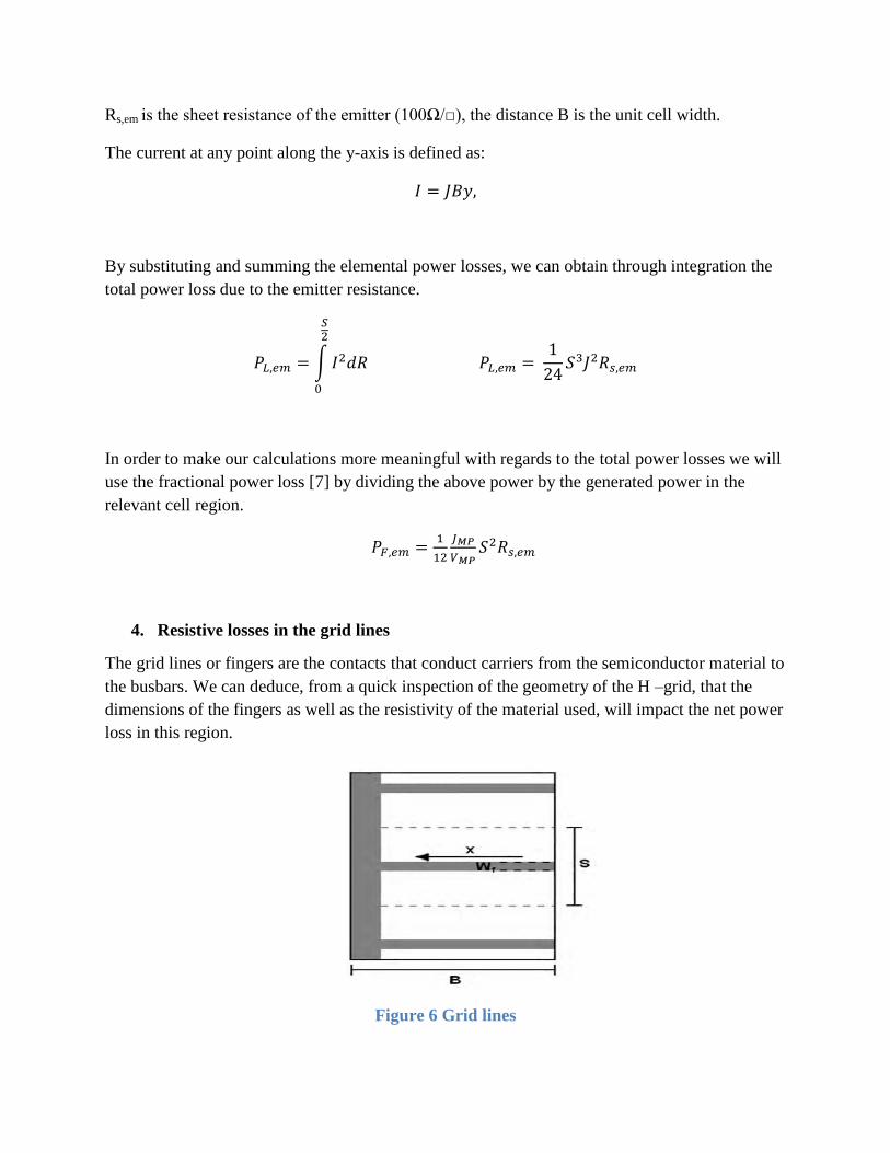
Rs,em is the sheet resistance of the emitter (100Ω/), the distance B is the unit cell width.
The current at any point along the y-axis is defined as:
By substituting and summing the elemental power losses, we can obtain through integration the
total power loss due to the emitter resistance.
∫
In order to make our calculations more meaningful with regards to the total power losses we will
use the fractional power loss [7] by dividing the above power by the generated power in the
relevant cell region.
4. Resistive losses in the grid lines
The grid lines or fingers are the contacts that conduct carriers from the semiconductor material to
the busbars. We can deduce, from a quick inspection of the geometry of the H –grid, that the
dimensions of the fingers as well as the resistivity of the material used, will impact the net power
loss in this region.
Figure 6 Grid lines
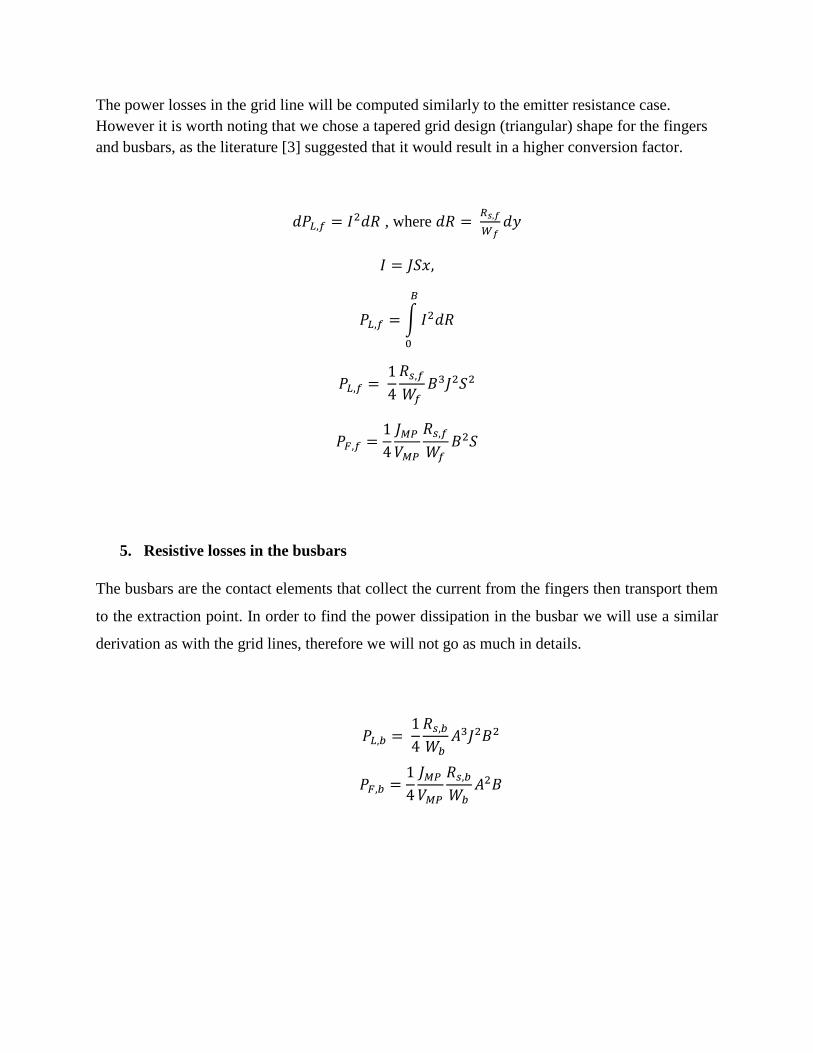
The power losses in the grid line will be computed similarly to the emitter resistance case.
However it is worth noting that we chose a tapered grid design (triangular) shape for the fingers
and busbars, as the literature [3] suggested that it would result in a higher conversion factor.
, where
∫
5. Resistive losses in the busbars
The busbars are the contact elements that collect the current from the fingers then transport them
to the extraction point. In order to find the power dissipation in the busbar we will use a similar
derivation as with the grid lines, therefore we will not go as much in details.
6. Shadowing losses of the fingers and busbars
The shadowing losses are the results in effective absorption area loss due to the contact grid. We
could evaluate them in terms of the total effective fractional loss introduced by the fingers and
busbars.
( )( )( ) ( )( )
However for optimization purposes we will consider separately the loss introduced by fingers
and busbars:
Where PF,sf and PF,sb are respectively the fractional shadowing losses due to the fingers and
busbars.
7. Optimization
With the use of differential calculus we can find the optimum width of busbars and fingers at
which the resistive losses are equal to the shadowing losses per unit cell. The resulting
expressions are provided in Serreze [3]:
√
√
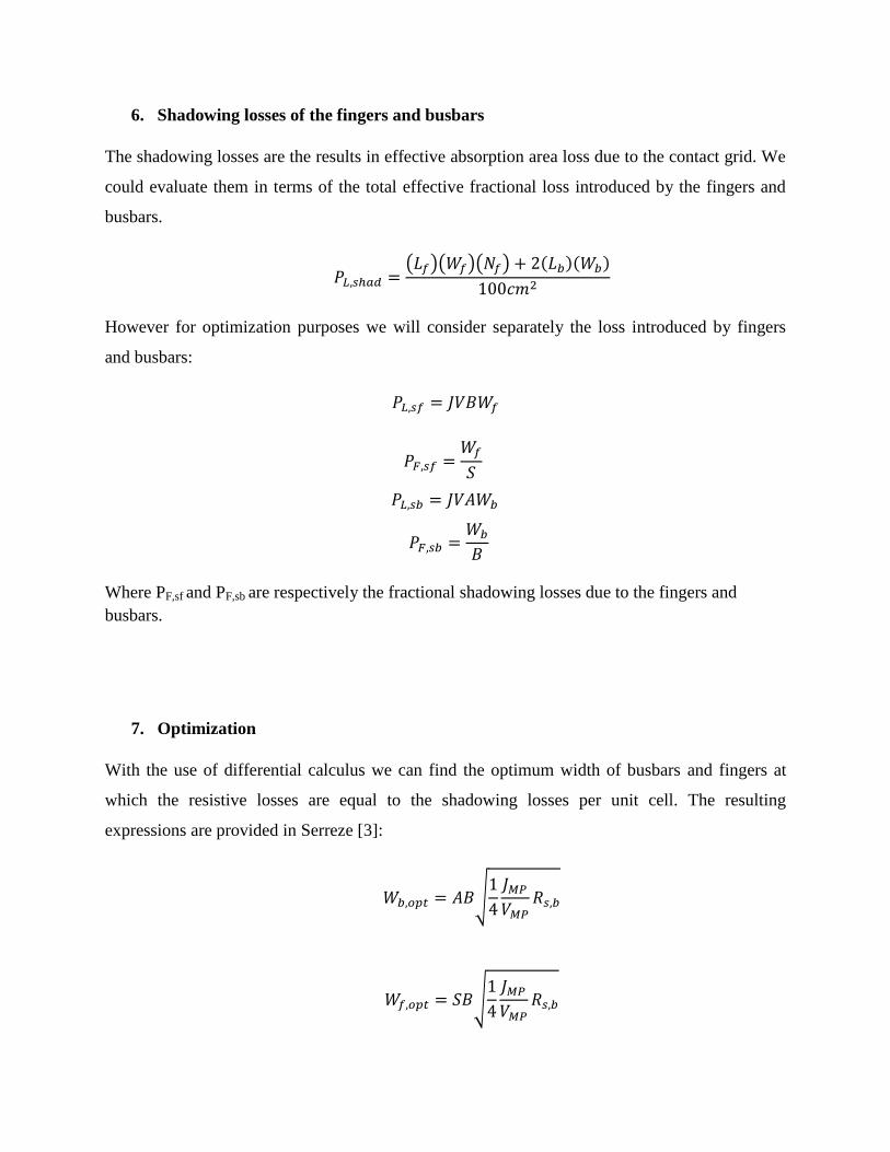
The sheet resistivity of the contact grid will be determined by the finger width as there is a limit
to the aspect ratio (
) achievable with screen printing. In order to find the optimal value of
finger spacing at minimum power loss, we could use an iterative approach given by Green [8].
However, we will use an interactive graphical application [9] that will take into account the
shading losses and the combined resistive losses on the emitter layer and fingers:
Figure 7 Optimization Curves

8. Results
Our contacts will be built through screen printing process using Dupont PV17A silver ink, which
has a maximum resistivity of 5*10-8
Ω m and emulsion thickness between 20 and 25µm. We will
pick the thickness of the paste in the fingers to be 100µm so that the effective sheet resistance of
the grid lines is: Rs,f = 0.5 mΩ/, and the thickness in the busbar will be 1mm so that the
effective sheet resistance of the busbars is Rs,b =50µΩ/.
Table 1: Final Grid design Parameters
variable value
Number of busbars 2
Busbar width (WF) 0.4319 mm
Busbar length 10 cm
Fingers width 60 µm
Fingers length 24.5 mm
Fingers Spacing 2 mm
Number of fingers 48
Table 2: Final Grid Losses
Emitter resistive losses 2 %
Busbars resistive losses 0.432 %
Busbars optical losses 1.728 %
finger resistive losses 0.155 %
Fingers optical losses 3 %
Total Power Losses 7.315 %
Manufacturing process
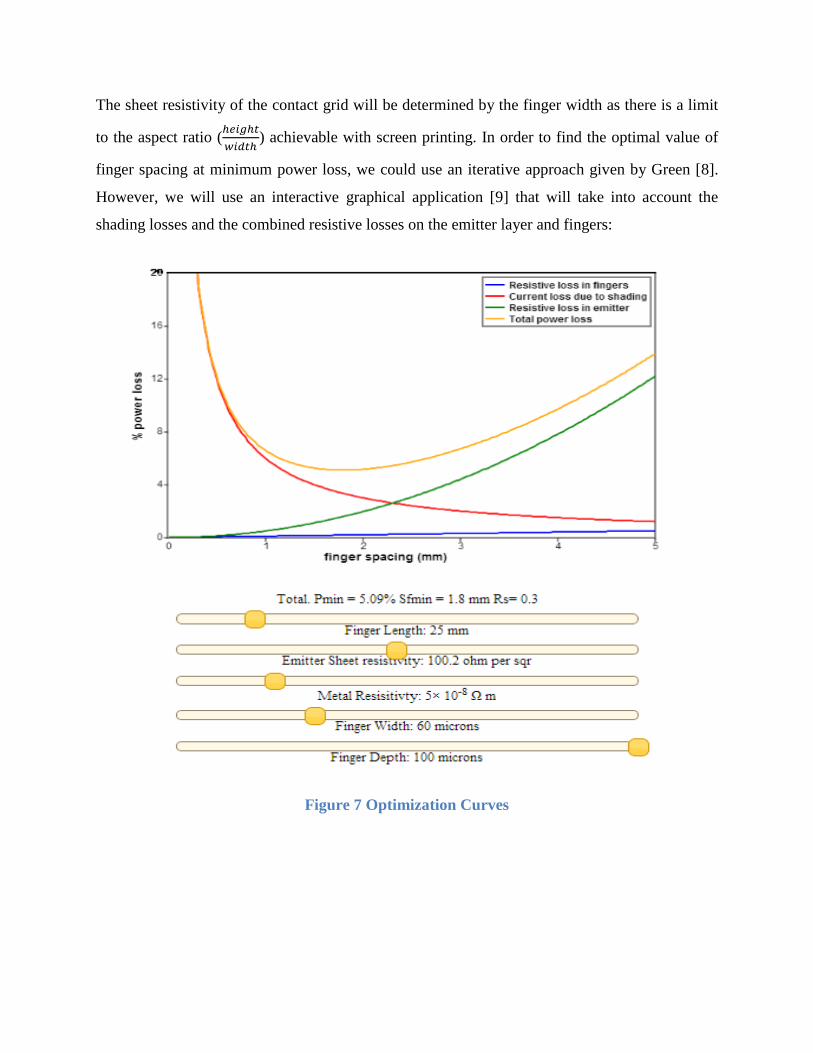
General Overview of the Screen-printing process
Screen-printing, a technique for creating the very fine circuit lines (that is, its fingers and
bus bars) on the front and back sides of the silicon wafer, has become one of the most common-
place methods of contact creation in organic photovoltaic (OPV) cells. The screen-printing
process consists of several major steps that can vary from production method to production
method; however, a basic guideline is followed by most major solar cell manufacturers. The first
step of the screen-printing process usually consists of creating the rear contact of the solar cell.
The rear contact is first covered with a screen that allows the chosen paste material to flow
through its openings; in many cases, the material used to create the rear contacts is aluminum.
The screen-printing mask used for the flow of the paste in the front/end side contacts of the solar
cell dictates the width and spacing of the fingers and bus bars. After the paste has been printed
into the rear portion of the solar cell, the wafer is exposed to a high temperature (several hundred
degrees Celsius, usually 750ºC-780ºC) firing process in order to fire (solder) the metal into the
silicon wafer. Furthermore, the wafer is exposed to drying at around 200ºC, depending on the
paste used. Then, the wafer is rotated and the front-end of the solar cell undergoes screen-
printing, similar to the previous steps. However, unlike the rear contact creation, silver paste is
commonly used as a screen-printing ink in this step. In order to accomplish the screen-printing
process, a squeegee is used in conjunction with the masking screen in order to allow the paste to
form the desired finger and bus bar widths and spacing on the front and rear-ends of the cell [10].
Figure 8 Squeege of Screen Printing

Finally, as with the rear contact, the front-side is exposed to a high temperature in order to fire
the metal into the silicon wafer. The resulting solar cell, with contacts on the front- and rear-side
is essentially the final product of the screen-printing process.
Figure 9 End Contact Grid
Project specifications and contact design ink
In terms of the group project's specifications and requirements, only the front-end of the
solar cell was taken into consideration. After performing extensive research, the team found that
one of the most efficient and commercially available silver inks to be used in a crystalline Silicon
(c-Si) wafer is the silver ink PV17A, manufactured by the chemical industry company DuPont™.
The company's Solamet®
photovoltaic metallization inks are readily available and suitable for
our design specifications; the PV17A ink, to be used for the front-side contact creation, is
designed for rapid dry and very fast (spike) firing. In addition, it provides excellent fine line
capabilities, high electrical conductivity after firing, excellent solderability and consistent
soldered adhesion, and reduced junction damage.
Screen-printing machine description
The machine used for screen-printing varies readily among manufacturers; however,
some components generally remain the same. Screen-printing machines have a “head”
component that act as the controller for printing speed, pressure, and height. The “base”

component acts as the bench for the process stability, where alignment takes place. The machine
controls, usually in the form of a touch-screen, include commands for contact printing, double-
printing (for example, when reducing bus bar width and increasing its height), parameter control,
etc. The specifications vary from machine to machine; some important characteristics to take into
consideration are the max printing area, max squeegee width, speed, and pressure, the cycle rate,
weight, compressed air, power, rated voltage, and so on. An example of a screen-printing
machine is the AUREL C1010D [11] screen printer, manufactured by AUREL Automation, an
Italy-based manufacturer of equipment and automation for the electronics industry. The data
sheet for the machine has been included in the appendix, where a more detailed description of
the machine can be observed.
Figure 10 Screen Printer
Processing conditions and parameters
The screen-printing process associated with our chosen ink, PV17A, follows a standard
model. The printing process lends itself to about 150-250 millimeters per second. The screen
type to be used must be 325 mesh stainless steel for >60 micrometer openings; for <60
micrometer openings, the mesh count should be 290 or 400. In addition, the drying step, which
takes into consideration the dryer machine and therefor the position of the wafer, lasts anywhere
from 1 minute to 10 minutes. For vertical dryers, the process lasts 10 minutes, with a drying
temperature of 170ºC-230ºC; for IR belt dryers, the process lasts 1 minute, with a drying
temperature of 150ºC-300ºC. The soldering is compatible with industry standard materials and

conditions. Finally, the firing of the ink into the metal encompasses a time of, ideally, under 8
seconds in order to ensure that a strong electrical contact to the wafer is established. In addition,
the thermal budget above the 600ºC threshold should be kept to a minimum. The typical firing
profile for the ink displays the peak temperature as a function of time [10].
Figure 11 Firing Profile
Conclusion
The findings presented in this paper allow the reader, as well as the team members, to have a
deeper understanding of the manufacturing process used for solar cell contact creation, the
analysis and break-down of power losses, and the general characteristics of the processes
involving in screen-printing of contacts onto solar cells. The preliminary problem to achieve a
total power loss of less than 10% due to ohmic losses, sheet resistance, and shadowing losses
was handled successfully. A total of 7.315% power loss was calculated by taking into
consideration the emitter resistive losses, the busbar resistive losses, the busbar optical losses, the
finger resistive losses, and the finger optical losses. In addition, the screen-printing ink PV17A
from DuPont was found to be a commercially viable option for our design. As such, the
conversion power of the solar cell was successfully optimized by creating an effective front-
contact design.
References
[1] “Hype Physics Solid State Electronics – PN Junction” [Online] Available :
http://hyperphysics.phy-astr.gsu.edu/hbase/solids/pnjun.html#c1
[2] "How A Photovoltic Cell Works" [Online]. Available:
http://inventors.about.com/library/inventors/blsolar3.htm
[3] H.B. Serreze. Optimizing solar cell performance by simultaneous consideration of grid
pattern design and interconnect configuration. In 13th IEEE Photovoltaic Specialists Conference,
pages 609–614, 1978.
[4] A.R. Burgers. How to design optimal metallization patterns for solar cells. Progress in
Photovoltaics, 7:457–461, 1999.
[5] A. Flat and G. Milnes. Optimization of multi-layer front-contact grid patterns for solar cells.
Solar Energy, 23:289–299, 1979.
[6] Sreenivasa Murty Dasari, Piyush Srivastav, Ravi Shaw, S. Saravanan, Prakash Suratkar,
Optimization of cell to module conversion loss by reducing the resistive losses, Renewable
Energy, Volume 50, February 2013, Pages 82-85, ISSN 0960-1481,
http://dx.doi.org/10.1016/j.renene.2012.05.022.
[7] M.A. Green. Solar Cells: Operating Principles, Technology and System Applications. The
University of New South Wales, Kensington, NSW, Australia, 1992.
[8] “PV education-Optimization of finger spacing” [Online] Available :
http://pveducation.org/pvcdrom/design/optimisation-of-finger-spacing
[9] “DuPont™ Solamet® PV17A photovoltaic metallization,” February 2012, [Online].
Available: http://www2.dupont.com/MCM/en_US/assets/downloads/prodinfo/PV17A.pdf
[10] “Aurel C1010D Screen Printer,” [Online]. Available: http://www.aurelautomation.com/wp-
content/uploads/2012/05/C1010D-web.pdf
[11] “Screen Printing For Crystalline Silicon Solar Cells,” April 2011, [Online]. Available:
http://www.appliedmaterials.com/sites/default/files/Screen_Printing_Backgrounder_0.pdf
[12] J. Toothman and S. Aldous, "How Stuff Works," 1 April 2001. [Online]. Available:
http://science.howstuffworks.com/environmental/energy/solar-cell3.htm.
[13] M. A. Green, "Silicon Solar Cells: Evolution, high-efficiency design and efficiency
enhancements," Kensington, 1992.
[14] V. Mehta, B. Sopori, R. Reedy, B. To, H. Moutinho and N. M. Ravindra, "Screen Printed Al
Contacts on Si Solar Cells: Issues and Some Solutions," vol. 1210, 2010.
[15] "The Power of the Sun: The Science of the Silicon Solar Cell," [Online]. Available:
http://science.sbcc.edu/physics/solar/sciencesegment/.
Related Documents